1
website:http://biz.LGservice.com
e-mail:http://www.LGEservice.com/techsup.html
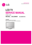
LCD TV
SERVICE MANUAL
CHASSIS : ML-041A
MODEL : RM-32LZ50
CAUTION
BEFORE SERVICING THE CHASSIS,
READ THE SAFETY PRECAUTIONS IN THIS MANUAL.
If you need more information on Computer and Electronic Repair, please visit these
websites to improve yourself.
http://www.fastrepairguide.com
http://www.protech2u.com
http://www.plasma-television-repair.com
http://www.lcd-television-repair.com
Happy Repairing!!
Highly Recommended Repair Ebook:
If you’re a LCD Monitor repairer, then this is the best guide for you.
Why? Because, the author revealed all his LCD Monitor Repairing
secrets for you. I think, with just few Repair tips you learned from
this guide you will get back your investment!
Click Here to read more.
This eBook will show you how to test the electronic component
correctly and accurately. Some of you may say that I don’t
need this eBook because it is too simple! Do you know that, in fact
there is lots of testing electronic components secrets I have learned
from this guide? Do you know how to test a‘TRIAC’ correctly and
accurately? If you answer no then I guess you have to get this
EBook. Click Here to read more.
Are you tired of searching the service manuals to look for the value
of a burnt resistor? If the answer is YES, then this eBook is a ‘must
have’ guide for you. You can save a lot of time and be able to repair
customer’s Electronic equipment with burnt resistors in it.
Click here to read more.
CONTENTS
CONTENTS .............................................................................................. 2
PRODUCT SAFETY ..................................................................................3
SPECIFICATION ........................................................................................6
TIMING CHART .......................................................................................10
ADJUSTMENT INSTRUCTION................................................................11
TROUBLE SHOOTING ............................................................................17
BLOCK DIAGRAM...................................................................................22
WIRING DIAGRAM ..................................................................................24
EXPLODED VIEW .................................................................................. 25
EXPLODED VIEW PARTS LIST ..............................................................26
REPLACEMENT PARTS LIST ............................................................... 27
SVC. SHEET ...............................................................................................
-2-
SAFETY PRECAUTIONS
IMPORTANT SAFETY NOTICE
Many electrical and mechanical parts in this chassis have special safety-related characteristics. These parts are identified by
in the
Schematic Diagram and Replacement Parts List.
It is essential that these special safety parts should be replaced with the same components as recommended in this manual to prevent
X-RADIATION, Shock, Fire, or other Hazards.
Do not modify the original design without permission of manufacturer.
General Guidance
Before returning the receiver to the customer,
An isolation Transformer should always be used during the
servicing of a receiver whose chassis is not isolated from the AC
power line. Use a transformer of adequate power rating as this
protects the technician from accidents resulting in personal injury
from electrical shocks.
always perform an AC leakage current check on the exposed
metallic parts of the cabinet, such as antennas, terminals, etc., to
be sure the set is safe to operate without damage of electrical
shock.
Leakage Current Cold Check(Antenna Cold Check)
It will also protect the receiver and it's components from being
damaged by accidental shorts of the circuitry that may be
inadvertently introduced during the service operation.
If any fuse (or Fusible Resistor) in this TV receiver is blown,
replace it with the specified.
When replacing a high wattage resistor (Oxide Metal Film Resistor,
over 1W), keep the resistor 10mm away from PCB.
Keep wires away from high voltage or high temperature parts.
With the instrument AC plug removed from AC source, connect an
electrical jumper across the two AC plug prongs. Place the AC
switch in the on position, connect one lead of ohm-meter to the AC
plug prongs tied together and touch other ohm-meter lead in turn to
each exposed metallic parts such as antenna terminals, phone
jacks, etc.
If the exposed metallic part has a return path to the chassis, the
measured resistance should be between 1MΩ and 5.2MΩ.
When the exposed metal has no return path to the chassis the
reading must be infinite.
An other abnormality exists that must be corrected before the
receiver is returned to the customer.
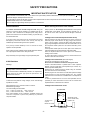
Leakage Current Hot Check (See below Figure)
X-RAY Radiation
Warning:
The source of X-RAY RADIATION in this TV receiver is the High
Voltage Section and the LCD PANEL.
For continued X-RAY RADIATION protection, the replacement
panel must be the same type panel as specified in the
Replacement Parts List.
To determine the presence of high voltage, use an accurate high
impedance HV meter.
Adjust brightness, color, contrast controls to minimum.
Measure the high voltage.
The meter reading should indicate
23.5 ¡ 1.5KV: 14-19 inch, 26 ¡ 1.5KV: 19-21 inch,
29.0 ¡ 1.5KV: 25-29 inch, 30.0 ¡ 1.5KV: 32 inch
If the meter indication is out of tolerance, immediate service and
correction is required to prevent the possibility of premature
component failure.
Plug the AC cord directly into the AC outlet.
Do not use a line Isolation Transformer during this check.
Connect 1.5K/10watt resistor in parallel with a 0.15uF capacitor
between a known good earth ground (Water Pipe, Conduit, etc.)
and the exposed metallic parts.
Measure the AC voltage across the resistor using AC voltmeter
with 1000 ohms/volt or more sensitivity.
Reverse plug the AC cord into the AC outlet and repeat AC voltage
measurements for each exposed metallic part. Any voltage
measured must not exceed 0.75 volt RMS which is corresponds to
0.5mA.
In case any measurement is out of the limits specified, there is
possibility of shock hazard and the set must be checked and
repaired before it is returned to the customer.
Leakage Current Hot Check circuit
AC Volt-meter
To Instrument's
exposed
METALLIC PARTS
0.15uF
1.5 Kohm/10W
-3-
Good Earth Ground
such as WATER PIPE,
CONDUIT etc.
SERVICING PRECAUTIONS
CAUTION: Before servicing receivers covered by this service
manual and its supplements and addenda, read and follow the
SAFETY PRECAUTIONS on page 3 of this publication.
NOTE: If unforeseen circumstances create conflict between the
following servicing precautions and any of the safety precautions on
page 3 of this publication, always follow the safety precautions.
Remember: Safety First.
General Servicing Precautions
1. Always unplug the receiver AC power cord from the AC power
source before;
a. Removing or reinstalling any component, circuit board
module or any other receiver assembly.
b. Disconnecting or reconnecting any receiver electrical plug or
other electrical connection.
c. Connecting a test substitute in parallel with an electrolytic
capacitor in the receiver.
CAUTION: A wrong part substitution or incorrect polarity
installation of electrolytic capacitors may result in an
explosion hazard.
2. Test high voltage only by measuring it with an appropriate high
voltage meter or other voltage measuring device (DVM,
FETVOM, etc) equipped with a suitable high voltage probe.
Do not test high voltage by "drawing an arc".
3. Do not spray chemicals on or near this receiver or any of its
assemblies.
4. Unless specified otherwise in this service manual, clean
electrical contacts only by applying the following mixture to the
contacts with a pipe cleaner, cotton-tipped stick or comparable
non-abrasive applicator; 10% (by volume) Acetone and 90% (by
volume) isopropyl alcohol (90%-99% strength)
CAUTION: This is a flammable mixture.
Unless specified otherwise in this service manual, lubrication of
contacts in not required.
5. Do not defeat any plug/socket B+ voltage interlocks with which
receivers covered by this service manual might be equipped.
6. Do not apply AC power to this instrument and/or any of its
electrical assemblies unless all solid-state device heat sinks are
correctly installed.
7. Always connect the test receiver ground lead to the receiver
chassis ground before connecting the test receiver positive
lead.
Always remove the test receiver ground lead last.
8. Use with this receiver only the test fixtures specified in this
service manual.
CAUTION: Do not connect the test fixture ground strap to any
heat sink in this receiver.
Electrostatically Sensitive (ES) Devices
Some semiconductor (solid-state) devices can be damaged easily
by static electricity. Such components commonly are called
Electrostatically Sensitive (ES) Devices. Examples of typical ES
devices are integrated circuits and some field-effect transistors and
semiconductor "chip" components. The following techniques
should be used to help reduce the incidence of component
damage caused by static by static electricity.
1. Immediately before handling any semiconductor component or
semiconductor-equipped assembly, drain off any electrostatic
charge on your body by touching a known earth ground.
Alternatively, obtain and wear a commercially available
discharging wrist strap device, which should be removed to
prevent potential shock reasons prior to applying power to the
unit under test.
2. After removing an electrical assembly equipped with ES
devices, place the assembly on a conductive surface such as
aluminum foil, to prevent electrostatic charge buildup or
exposure of the assembly.
3. Use only a grounded-tip soldering iron to solder or unsolder ES
devices.
4. Use only an anti-static type solder removal device. Some solder
removal devices not classified as "anti-static" can generate
electrical charges sufficient to damage ES devices.
5. Do not use freon-propelled chemicals. These can generate
electrical charges sufficient to damage ES devices.
6. Do not remove a replacement ES device from its protective
package until immediately before you are ready to install it.
(Most replacement ES devices are packaged with leads
electrically shorted together by conductive foam, aluminum foil
or comparable conductive material).
7. Immediately before removing the protective material from the
leads of a replacement ES device, touch the protective material
to the chassis or circuit assembly into which the device will be
installed.
CAUTION: Be sure no power is applied to the chassis or circuit,
and observe all other safety precautions.
8. Minimize bodily motions when handling unpackaged
replacement ES devices. (Otherwise harmless motion such as
the brushing together of your clothes fabric or the lifting of your
foot from a carpeted floor can generate static electricity
sufficient to damage an ES device.)
General Soldering Guidelines
1. Use a grounded-tip, low-wattage soldering iron and appropriate
tip size and shape that will maintain tip temperature within the
range or 500¡£
F to 600¡£
F.
2. Use an appropriate gauge of RMA resin-core solder composed
of 60 parts tin/40 parts lead.
3. Keep the soldering iron tip clean and well tinned.
4. Thoroughly clean the surfaces to be soldered. Use a mall wirebristle (0.5 inch, or 1.25cm) brush with a metal handle.
Do not use freon-propelled spray-on cleaners.
5. Use the following unsoldering technique
a. Allow the soldering iron tip to reach normal temperature.
(500¡£
F to 600¡£
F)
b. Heat the component lead until the solder melts.
c. Quickly draw the melted solder with an anti-static, suctiontype solder removal device or with solder braid.
CAUTION: Work quickly to avoid overheating the
circuitboard printed foil.
6. Use the following soldering technique.
a. Allow the soldering iron tip to reach a normal temperature
(500¡£
F to 600¡£
F)
b. First, hold the soldering iron tip and solder the strand against
the component lead until the solder melts.
c. Quickly move the soldering iron tip to the junction of the
component lead and the printed circuit foil, and hold it there
only until the solder flows onto and around both the
component lead and the foil.
CAUTION: Work quickly to avoid overheating the circuit
board printed foil.
d. Closely inspect the solder area and remove any excess or
splashed solder with a small wire-bristle brush.
-4-
IC Remove/Replacement
Some chassis circuit boards have slotted holes (oblong) through
which the IC leads are inserted and then bent flat against the
circuit foil. When holes are the slotted type, the following technique
should be used to remove and replace the IC. When working with
boards using the familiar round hole, use the standard technique
as outlined in paragraphs 5 and 6 above.
Removal
1. Desolder and straighten each IC lead in one operation by gently
prying up on the lead with the soldering iron tip as the solder
melts.
2. Draw away the melted solder with an anti-static suction-type
solder removal device (or with solder braid) before removing the
IC.
Replacement
1. Carefully insert the replacement IC in the circuit board.
2. Carefully bend each IC lead against the circuit foil pad and
solder it.
3. Clean the soldered areas with a small wire-bristle brush.
(It is not necessary to reapply acrylic coating to the areas).
"Small-Signal" Discrete Transistor
Removal/Replacement
1. Remove the defective transistor by clipping its leads as close as
possible to the component body.
2. Bend into a "U" shape the end of each of three leads remaining
on the circuit board.
3. Bend into a "U" shape the replacement transistor leads.
4. Connect the replacement transistor leads to the corresponding
leads extending from the circuit board and crimp the "U" with
long nose pliers to insure metal to metal contact then solder
each connection.
Power Output, Transistor Device
Removal/Replacement
1. Heat and remove all solder from around the transistor leads.
2. Remove the heat sink mounting screw (if so equipped).
3. Carefully remove the transistor from the heat sink of the circuit
board.
4. Insert new transistor in the circuit board.
5. Solder each transistor lead, and clip off excess lead.
6. Replace heat sink.
Circuit Board Foil Repair
Excessive heat applied to the copper foil of any printed circuit
board will weaken the adhesive that bonds the foil to the circuit
board causing the foil to separate from or "lift-off" the board. The
following guidelines and procedures should be followed whenever
this condition is encountered.
At IC Connections
To repair a defective copper pattern at IC connections use the
following procedure to install a jumper wire on the copper pattern
side of the circuit board. (Use this technique only on IC
connections).
1. Carefully remove the damaged copper pattern with a sharp
knife. (Remove only as much copper as absolutely necessary).
2. carefully scratch away the solder resist and acrylic coating (if
used) from the end of the remaining copper pattern.
3. Bend a small "U" in one end of a small gauge jumper wire and
carefully crimp it around the IC pin. Solder the IC connection.
4. Route the jumper wire along the path of the out-away copper
pattern and let it overlap the previously scraped end of the good
copper pattern. Solder the overlapped area and clip off any
excess jumper wire.
At Other Connections
Use the following technique to repair the defective copper pattern
at connections other than IC Pins. This technique involves the
installation of a jumper wire on the component side of the circuit
board.
1. Remove the defective copper pattern with a sharp knife.
Remove at least 1/4 inch of copper, to ensure that a hazardous
condition will not exist if the jumper wire opens.
2. Trace along the copper pattern from both sides of the pattern
break and locate the nearest component that is directly
connected to the affected copper pattern.
3. Connect insulated 20-gauge jumper wire from the lead of the
nearest component on one side of the pattern break to the lead
of the nearest component on the other side.
Carefully crimp and solder the connections.
CAUTION: Be sure the insulated jumper wire is dressed so the
it does not touch components or sharp edges.
Diode Removal/Replacement
1. Remove defective diode by clipping its leads as close as
possible to diode body.
2. Bend the two remaining leads perpendicular y to the circuit
board.
3. Observing diode polarity, wrap each lead of the new diode
around the corresponding lead on the circuit board.
4. Securely crimp each connection and solder it.
5. Inspect (on the circuit board copper side) the solder joints of
the two "original" leads. If they are not shiny, reheat them and if
necessary, apply additional solder.
Fuse and Conventional Resistor
Removal/Replacement
1. Clip each fuse or resistor lead at top of the circuit board hollow
stake.
2. Securely crimp the leads of replacement component around
notch at stake top.
3. Solder the connections.
CAUTION: Maintain original spacing between the replaced
component and adjacent components and the circuit board to
prevent excessive component temperatures.
-5-
SPECIFICATION
NOTE : Specifications and others are subject to change without notice for improvement.
1. Application range
This specification is applied to ML-041A chassis.
2. Requirement for Test
Testing for standard of each part must be followed in below
condition.
(1) Temperature: 25°C ± 2°C
(2) Humidity: 65% ± 10%
(3) Power: Standard input voltage (AC 100-240V, 50/60Hz)
(4) Measurement must be performed after heat-run more than
30min.
(5) Adjusting standard for this chassis is followed a special
standard.
3.General Specification(TV)
No.
1
Item
Video input applicable system
Specification
Remark
1)PAL-D/K,B/G,I
2)NTSC-M
3)SECAM NTSC 4.43’
2
Receivable broadcasting system
1)PAL/SECAM BG
EU/Non-EU(RZ/RT)
2)PAL/SECAM DK
(PAL Market)
3)PAL I/I
4)SECAM L/L’
5)NTSC M
6)PAL-N/M
7)NTSC Area(RM)
7)NTSC M
3
RF input channel
VHF : E2 ~ E12
UHF : E21 ~ E69
PAL
CATV : S1 ~ S20
HYPER : S21 ~ S41
L/L’ : B,C,D
FRANCE
VHF : 2 ~ 13
UHF : 14 ~ 69
NTSC
CATV : 1 ~ 125
VHF Low : 1~M10
JAPAN
VHF High : 4~S22
UHF : S23~62
4
Input voltage
AC 100 - 240V/ 50Hz,60HZ
5
Picture size
800.4 mm
31.51”
6
Tuning system
FVS 100 program
PAL, 200PR.(Option)
FS
NTSC
7
Operting environment
8
Storage environment
9
Display
1)Temp : 0 ~ 40 deg
2)Humidity : 85%
3)Temp : -20 ~ 60 deg
4)Humidity : 85%
LCD Module
-6-
LPL
5.General Specification(Monitor)
No.
Item
Specification
1
Panel
32” TFT WXGA LCD
2
Frequency range
H: 31 ~ 61KHz, V: 56 ~ 75Hz
3
Control function
Unit
Remark
DVI-I input
1) Contrast/ Brightness
2) H- Position/ V-Position
3) Tracking : Clock/Phase
4) Auto Configure
5) Reset
1: Y
4
Component Jack
3: Pb
5: Pr
Middle east
7: Line1 Ready
/NTSC Only
9: LINE2
11: LINE3
13: Line3 Ready
2: Y GND
D4 Jack
4: Pb GND
(525i,525p,750p,1125i)
6: Pr GND
8: LINE1
Japan only
10: Line2 Ready
12: SWITCH GND
14: SWITCH
5
H/V-Sync
Video
Power consumption
Power ON
ON/ON
Active
≤ Max 170
W
Green
Stand by
OFF/ON
OFF
≤ 3.0
W
Red
DPMS Mode
ON/OFF
OFF
≤typ.30
W
Green
-
-
-
W
*.
LPL
760.0 x 450.0 x 48.0
Power off
Type
Size
6
LED
mm
LCD Module
Pixel Pitch
LPL
0.1702 x 0.5107 x RGB
mm
Pixel Format
1366 horiz. By 768 vert. pixels
RGB strip arrangement
Coating
Hard coating(3H), Anti-glare
treatment of the front polarizer
Back Light
LPL
-7-
16EEFL
(H) x (V) x (D)
6.Optical Feature(LCD Module)
No.
Item
Specification
Remark
LPL
1
Viewing Angle
2
Luminance
R/L, U/D
176,176
<CR 10>
3
Contrast Ratio
4
CIE Color Coordinates
Luminance(cd/ )
500
Typical
Variation
1.3
MAX/MIN
350
ALL white/All back
WHITE
RED
Green
Blue
WX
Typ.
0.285
WY
Typ.
0.293
Wr
Typ.
0.640
Yr
Typ.
0.341
Xg
Typ.
0.287
Yg
Typ.
0.610
Xb
Typ.
0.146
Yb
Typ.
0.069
LPL
7.Feature and Function
No.
Item
Specification
Remark
TOP, FLOF, LIST 10 page
Top(option)
NEC code
PAL/NTSC
1
Teletext
2
REMOCON
3
AV input
1
Rear(RT/RM)
4
S-AV input
1
Side
5
Component input
2
Side, Rear(RT/RM)
6
PERI TV connector
Half SCART: 1
Rear(RZ)
7
PERI TV connector
Full SCART: 1
Rear(RZ)
8
RGB input
1
DVI
9
RS-232
1
D-Sub 9 pin(RM)
10
Discrete IR
1
(RM)
11
D-sub audio input
1
Stereo
12
2 Carrier stereo
BG,DK
13
NICAM stereo
BG,I,LL’
14
2 Carrier dual
BG,DK
15
NICAM dual
BG,I,LL’
16
DW(Double Window) mode
X
17
MW(Multi Window) mode
X
18
Film mode
O
19
Noise reduction
X
20
Progressive scan
O
21
Motion detection
O
22
SRS WOW
X
23
Swivel Speaker
X
24
EZ-pip
25
Local Key
X
Pr+/-, vol+/-, ok, menu, tv/av, power
-8-
8.Component Video Input (Y, PB, PR)
NO
Resoluton
H-freq(kHz)
V-freqHz)
1
640 x 480
15.73
60.00
SDTV. DVD 480i
RZ, RT, RM
2
640 x 480
15.63
59.94
SDTV. DVD 480i
RZ, RT, RM
3
704 x 480
31.47
59.94
EDTV 480p
RT, RM
4
720 x 576
15.625
50.00
SDTV. DVD 625 Line
RZ, RT, RM
5
720 x 576
31.25
50.00
HDTV 576p
RT, RM
6
1280 x 720
45.00
60.00
HDTV 720p
RT, RM
7
1280 x 720
44.96
59.94
HDTV 720p
RT, RM
8
1920 x 1080
31.25
50.00
HDTV 1080i 50Hz(For Australia)
RT, RM
9
1920 x 1080
33.75
60.00
HDTV 1080i 60Hz(ATSC)
RT, RM
10
1920 x 1080
33.72
59.94
HDTV 1080i 59.94Hz
RT, RM
V-freq(Hz)
Pixel clock
Proposed
9.PC Input Mode
NO
Resoluton
H-freq(kHz)
Pixel clock(MHz)
1
640 x 480
31.469
59.94
25.17
VESA(VGA)
2
640 x 480
37.879
60.31
40.00
VESA(SVGA)
3
640 x 480
48.363
60.00
65.00
VESA(XGA)
4
800 x 600
47.693
60.00
81.15
VESA(WXGA)
5
800 x 600
47.649
59.936
84.625
VESA(WXGA)
6
800 x 600
33.75
60.00
86.375
HDCP DVI Digital 1080i(RM Only)
7
800 x 600
45.00
60.00
74.375
HDCP DVI Digital 720P(RM Only)
Proposed
DVI-PC, Analog RGB, Digital RGB
-9-
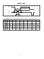
TIMING CHART
VIDEO
A
E
D
B
SYNC
C
<< Dot Clock (MHz), Horizontal Frequency (kHz), Vertical Frequency (Hz), Horizontal etc... (µs), Vertical etc... (ms) >>
Mode
1
2
3
4
H/V
Sort
Sync
Polarity
H
+
V
–
H
+
V
+
H
–
V
H
–
+
V
–
Dot
Clock
25.175
40.0
65.0
79.50
Frequency
Total Period Video Active Time
(E)
(A)
Front Porch
(B)
Sync Duration
(D)
Back Porch
(F)
31.469
800
640
16
96
48
59.94
525
480
10
2
33
37.879
1056
800
40
128
88
60.317
628
600
1
4
23
48.363
1344
1024
24
136
160
60.004
47.776
806
1664
768
1280
3
64
6
128
29
192
59.870
798
768
3
7
20
- 10 -
Resolution
640x480
800x600
1024x768
1280x768
ADJUSTMENT INSTRUCTION
1. Application Object
2.2.1 EDID DATA
[DDC DATA Analog]
This instruction is for the application to the LCD TV.
2. Adjustment
00
01
03
04
05
00
00
FF FF FF
02
FF
FF FF 00
06
07
08
1E 6D 45
09
0A 0B 0C 0D
10
00
0E 01
03
01
40
26
78
08
40
75
0E 0F
01
01
01
01
B1
DA A1 56
48
98
24
20
13
48
4B A1
08
00
31
01
01
01
01
45
40
01
01
2.1 PC Auto Gain/Offset adjustment
30
61
40
81
80
01
01
4E 1F 00
90
51
00
1B 30
40
88
2.1.1 Adjustment preparation
40
13
00
A2 0B
32
00
00
18
1B 21
50
A0 51
00
1) Heat Run after 30 minutes execution of white pattern
2) Pattern generator is connected to the DVI Jack of LCD TV.
3) To use Pattern Generator(801GF, VG819) the resolution is
XGA(1024 X 768), this pattern gives 16gradation grey
scale or 16 gradation which follows in the VG819.
4) For (SVC) Adjustment first convert into adjustment mode
and after converting press IN-START Key and VOL+ Key
consequtively from Auto gain menu.
5) fter adjustment is complete pressing enter key stores and
completes the process.
50
48
88
35
00
A2
0B 32
00
00
1C 00
00
00
FD 00
60
3D
1F 30
09
00
0A 20
20
20
20
20
20
00
00
00
FC
70
00
52
4D 33
32
4C 5A 35
30
0A
20
20
20
20
00
ED
08
09
0A 0B 0C 0D
00
01
03
04
05
00
FF FF FF
FF
FF FF 00
1E 6D 46
10
00
0E 01
03
81
40
26
78
08
20
13
48
4B A1
08
00
31
40
30
61
40
81
80
01
01
2.1 Video Auto Gain/Offset adjustment
40
13
00
A2 0B
32
00
00
1) Heat Run after 30 minutes execution of white pattern
2) In RF mode using adjustment remote controller Push INSTART Key. And again push IN-Start Key.
3) Gray Scale Pattern appears and then press vol+ key, to
adjust Auto-again.
4) After adjusting press enter to save the values of auto-gain.
50
48
88
35
00
A2
0B 32
60
3D
1F 30
09
00
0A 20
70
00
52
4D 33
32
1) Connect D-Sub to DVI-I Cable to DVI-I Jack.
2) Input analog signal and check pc video in the screen.
3) After appearing the pc video, write Analog EDID data.
4) Connect DVI D Cable to DVI Jack..
5) Input digital signal and check pc video in the screen.
6) After appearing the pc video, write digital EDID data.
3B
[DDC DATA Digital]
00
2.2 EDID (The Extended Display Identification Data) setting
1E 30
02
06
07
75
0E 0F
01
01
01
01
B1
DA A1 56
48
98
24
01
01
01
01
45
40
01
01
4E 1F 00
90
51
00
1B 30
40
88
18
1B 21
50
A0 51
00
00
00
1C 00
00
00
FD 00
20
20
20
20
20
00
00
00
FC
4C 5A 35
30
0A
20
20
20
20
00
6C
1E 30
38
2.3 HDCP (High-Bandwidth Digital Contents Protection) Set
2.3.1 HDCP DVI(Digital Visual Interface) is the link which
transmits HD video of HD and STB when in sleep
mode.
This function prevents the hazard of hang display thus
securing the security against the contents and copy
protection.
2.3.2 To store in EEPROM(AT24C16) in HDCP function
connect DVI cable.Detailed work content from work
map reference.
Note. : HDCP will temporarily exclude in spec.
HDCP will apply from USA Product later. (Only USA)
- 11 -
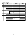
3. Shipping Conditions
NO
ITEM
CONDITION
1
Power
Off
2
Volume Level
30
3
Main Pcture Input
TV
5
Main Last Channel
Pr 01
8
Mute
Off
9
ARC
10
Station
REMARK
16:9
Auto Program
Manual Program
Program Edit
11
Picture
Favorite Program
None
PSM
Dynamic
Dynamic
14
15
16
Sound
Special
PC
Contrast
80
Brightness
40
Colour
70
Sharpness
70
Tint
0
SSM
Flat
AVL
Off
Balance
0
Input
TV
Child Lock
Off
Auto sleep
Off
Language
English(Area Management)
H-Position
V-Position
Variable by each mode
Clock
Phase
Auto Configure
- 12 -
NTSC OPTION
*Option(PAL)
NO
ITEM
CONDITION
REMARK
NO
ITEM
Option 1
1
2
3
4
5
6
7
8
Side AV
SCART
PC
SideComp
16:9
200PR
Text
ACMS
1
1
1
1
1
0
1
1
CONDITION
Option 3
0: Side AV Off
1
Language
1
HiDev
0
2
Hotel
0
3
Top
1
4
I II SAVE
1
1: EU5
0: SCART Off
2: 12 nations(Europe)
1: SCART On
3: Eng + Chines
0: PC Off
4: Eng + Arab + Urdu
1: PC On
5: Eng + FARSI
0: SideComp Off
2
Txt Lang
0
Turbo Vol
0
6
Ch/Aus
0
0: WEST EU
1: SideComp On
1: EAST EU 1
0: Wide Off
2: TURKY EU
1: Wide On
3: EAST EU 2
0: 100 Program
4: CYRILLIC 1
1: 200 Program
5: CYRILLIC 2
0: Text Off
6: CYRILLIC 3
1: Text On
7: TURKY GRE 1
0: ACMS On
8: TURKY GRE 2
1: ACMS Off
9: TURKY GRE 3
10: ARAB FRAN
0: HiDev Off
11: ARAB ENG
1: HiDev On
12: ARAB HEB 1
0: Hotel Off
13: ARAB HEB 2
1: Hotel On
14: FARSI ENG
0: Top Off
15: FARSI FRA
1: Top On
5
0: Eng Only
1: Side AV On
Option 2
1
REMARK
16: FARI ALL
0: Ch. Sound Non Memory
3
Inch opt
0
reserved
1: Ch. Sound Memory
4
DDCi
Analog
Analog: Analog
Digital: Digital
0: except below area(Off)
1: Middle-east Area Vol On
0: except below area(Off)
1: China, Australia On
- 13 -
*Optionel(NTSC)
NO
1
ITEM
Side-AV
CONDITION
0
REMARK
0 : Component2 ON
1 : Video2 On
2
ToolOption
0
0 : 50/41 Tool
1 : 30 Tool
3
HDCP
1
0 : HDCP ON
1 : HDCP OFF
4
Speaker Output
1
0 : Speaker Output => 3W
1 : Speaker Output => 5W
5
DownLoad
0
0 : DownLoad Off
1 : DownLoad ON
6
Country
2
0 : Japan
1 : Korea
2 : North America
3 : Central and South America
7
Canadian Vchip
1
0 : V-Chip Function Off
8
Screen Size
1
0 : 4 :3 Mode
9
S-Video
1
0 : S-Video Off
10
Com Filter
1
0 : Com-Filter Off
1 : V-Chip Function ON
1 : 16 : 9 Mode
1 : S-Video on
1 : Com-Filter ON
- 14 -
EDID ADJUSTMENT
Windows EDID V1.0 User Manual
2. EDID Read & Write
1) Run WinEDID.exe
Operating System: MS Windows 98, 2000, XP
Port Setup: Windows 98 => Don’t need setup
Windows 2000, XP => Need to Port Setup.
This program is available to LCD Monitor only.
1. Port Setup
a) Copy “UserPort.sys” file to
“c:\WINNT\system32\drivers” folder
b) Run Userport.exe
2) Edit Week of Manufacture, Year of Manufacture,
Serial Number
a) Input User Info Data
b) Click “Update” button
c) Click “ Write” button
c) Remove all default number
d) Add 300-3FF
PB
PR
R
AUDIO
L
COMPONENT
DVD IN(480i/576i)
Y
S-VIDEO
e) Click Start button.
f) Click Exit button.
A
9
IBM
Compatible PC
Video Signal
Generator
15
10
5
1
C
13
us
ed
PARALLEL PORT
1
32
C
25
RS
2
5V
OFF
14
ON
F
LL
EL
No
t
6
5
RA
C
PA
5V
Power inlet (required)
ON
R
220
WE
VG
ST
A
PO
S
MO
NIT
OR
B
V-S
YN
C
Control Line
11
6
1
Power Select Switch
(110V/220V)
Power LED
E
4.7K
OFF
74LS06
E ST Switch
B
F V-Sync On/Off Switch
(Switch must be ON.)
Figure 1. Cable Connection
- 15 -
4.7K
4.7K
5V
74LS06
SVC REMOCON
NO
1
2
3
4
5
6
7
8
9
10
11
12
13
14
15
16
17
18
19
20
21
22
23
24
25
26
27
28
29
30
31
32
33
34
35
36
37
38
KEY
FUNTION
REAMARK
To turn the TV on or off
POWER
To turn the TV on automatically if the power is supplied to the TV. (Use the
POWER ON
POWER key to deactivate): It should be deactivated when delivered.
To activate the mute function.
MUTE
To check TV screen image easily.
P-CHECK
To check TV screen sound easily
S-CHECK
To select size of the main screen (Normal, Spectacle, Wide or Zoom)
ARC
Switch to closed caption broadcasting
CAPTION
To toggle on/off the teletext mode
TXT
To select an external input for the TV screen
TV/AV
To start turbo sound
TURBO SOUND
TURBO PICTURE To start turbo picture
To enter adjustment mode when manufacturing the TV sets.
To adjust the screen voltage (automatic):
In-start mute Adjust AV(Enter into W/B adjustment mode)
IN-START
W/B adjustment (automatic):
After adjusting the screen W/B adjustment Exit two times (Adjustment completed)
To enter into the adjustment mode. To adjust horizontal line and sub-brightness.
ADJ
To select the multiple sound mode (Mono, Stereo or Foreign language)
MPX
To release the adjustment mode
EXIT
To easily adjust the screen according to surrounding brightness
APC(PSM)
To easily adjust sound according to the program type
ASC(SSM)
To check component input
MULTIMIDIA
To check the front AV
FRONT-AV
To move channel up/down or to select a function displayed on the screen.
CH¡
To adjust the volume or accurately control a specific function.
VOL¡
To set a specific function or complete setting.
ENTER
To move the channel down in the PIP screen.
PIP CH-(OP1)
To use as a red key in the teletext mode
To move the channel in the PIP screen
PIP CH+(OP2)
To use as a green key in the teletext mode
To switch between the main and sub screens
PIP SWAP(OP3)
To use as a yellow key in the teletext mode
To select the input status in the PIP screen
PIP INPUT(OP4)
To use as a blue key in the teletext mode
To set a function that will automatically adjust screen status to match
EYE
the surrounding brightness so natural color can be displayed.
To select the functions such as video, voice, function or channel.
MENU
To set the delivery condition status after manufacturing the TV set.
IN-STOP
To halt the main screen in the normal mode, or the sub screen at the PIP screen.
STILL
Used as a hold key in the teletext mode (Page updating is stopped.)
Displays the teletext time in the normal mode
TIME
Enables to select the sub code in the teletext mode
Used as the size key in the PIP screen in the normal mode
SIZE
Used as the size key in the teletext mode
Used as the index key in the teletext mode (Top index will be
MULTI PIP
displayed if it is the top text.)
To select the position of the PIP screen in the normal mode
Used as the update key in the teletext mode (Text will be
POSITION
displayed if the current page is updated.)
Used as Mode in the teletext mode
MODE
To select the simultaneous screen
PIP
To adjust screen tilt
TILT
To manually select the channel.
0~9
- 16 -
Shortcut keys
Shortcut keys
Shortcut keys
Use the AV
key to enter
the screen
W/B
adjustment
mode.
Shortcut keys
Shortcut keys
Shortcut keys
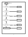
TROUBLESHOOTING
No power
(LED indicator off)
Check 24V or 12V
of Power B/D
:[A]Process
Faill
Check short of main B/D
or Change Power B/D
Pass
Check Output of
L3, L1300
Change L3, L1300
Faill
Pass
Check Output of
IC1300, IC4 or IC8
Change IC1300,IC4 or IC8
Faill
Faill
Pass
Change LED Assy
Check LED Assy
Faill
Pass
Check P101 Connector
- 17 -
Change L808,L809
(F801,F802)
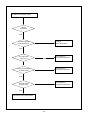
No Raster
:[B]Process
Check LED Status
on display unit
Check L900,L901
L902,L903
Repeat A PROCESS
Faill
Faill
Change L900,L901,
L902,L903
Pass
Check the input/
Output of IC901
Change IC901
Faill
Pass
Check inverter
Connector or inverter
Faill
Change inverter
connector or inverter
Faill
Change panel link
cable or module
Pass
Check panel link
Cable or module
Pass
Check input source cable and jack
Faill
- 18 -
Change module
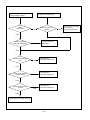
No Raster on Component signal
Repeat
[A] Process
Pass
Check the signal of
Q310,Q315,Q316
Faill
Change
Q310,Q315,Q316
Check the input/
output of IC1
Faill
Re-soldering or
Change the defect part
Check the input/output
of IC500, IC600
Faill
Re-soldering or
Change the defect part
Faill
Re-soldering or
Change the defect part
Pass
Pass
Check the input/
output of IC901
Pass
Check input source cable and jack
- 19 -
No Raster on AV Signa
(Video1,Video2, S-Video)
Repeat
[A] Process
No Raster on TV(RF) signal
Faill
Check the output of
TU1000
Pass
Check the signal of
C316,C317,Q308,Q313
Faill
Change C316,C317,
Q308,Q313
Pass
Check the input/output
of IC1
Faill
Re-soldering or
Change the defect part
Faill
Re-soldering or
Change the defect part
Faill
Re-soldering or
Change the defect part
Pass
Check the input/output
of IC500, IC600
Pass
Check the input/output
of IC901
Pass
Check input source cable and jack
- 20 -
Faill
Check 5V, 33V of TU1000
Re-soldering or
Change the defect part
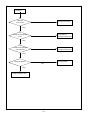
No Sound
Check the
input source
Faill
Change source input
Pass
Check the input/output
of IC1
Faill
Re-soldering or
Change the defect part
Faill
Re-soldering or
Change the defect part
Pass
Check the input/output
of IC100,IC101
Pass
Check the speaker
Faill
Pass
Check the speaker wire
- 21 -
Change speaker
- 22 -
PC_ LR
CVBS_L,R
SIDE_ LR
HD_COMP _ L,R
CVBS_IN
SIDE_Y,C
SIDE_COMP
NTSC _ IF
HD_COMP (NT)
PC_R,G,B
DVI
LA7222C
(IC200)
8
SM5301
(IC800)
3
R,G,B
R
L
8
8
8
(IC100,IC101)
B
G
R
R,G,B
M52758
S/W
(IC850)
MST9883
ADC
(IC600)
MPS7720
AMP
VCT49xyI 3D_Comb_Y,C
VCTI
TC90A65F
2
(IC1)
3D Comb
VCTi_Video out
(IC450)
3
R,G,B
HD_Y,Pb,Pr 3
PC_R,G,B 3
DVI
3
RAM
(IC501)
FLI2300
(IC500)
R,G,B 3
ROM
(IC900)
GM5221
SCALER
(IC901)
LVDS
or TTL
OUT
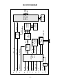
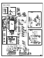
BLOCK DIAGRAM
BLOCK DIAGRAM DESCRIPTION
1. Video controller unit and display data conversion unit
The video controller unit recives the video signal input from the tuner, AV port (CVBS ,S-Videoand component ).
Comb fiter separates the YC component. The composite signal from the vcti goes to the 3-D comb filter and
comb filter gives YC signal as output which goes back to the Vcti. Vcti converts it to the analog RGB signal
through the microcomputer (Vcti) combined with the video decoder that integrates various functions in one chip.
Y,Pb,Pr signal from the component jack goes directly to the switch( SM5301) which makes switching between
the two signals YpbPr and RGB which comes form the vcti.Output of this switch depends on the selected
mode.If the mode selected is component the it gives YPbPr as the output otherwise it gives RGB signal.
Then, it is inputted to the AD converter (AD9883) and generates the 4:4:4 format digital signal. This digital signal
is inputted to the picture enhancer (FLI2300), which processes the video signal and converts the image quality
enhanced data to an analog RGB signal again before displaying it.
The image quality enhanced de-interlace signal is inputted to the scaler (GM5221) and converted to the LVDS
signal by the integrated LVDS IC before being sent to the LCD module.
VCTI is the main microcomputer that processes both video signals and sound signals. It also processes the RF
signal received from the tuner.
The scaler enables to adjust timing on the LCD panel, as well as an adjustment of the size and position of the
input signal.
The graphic controller unit receives the PC (analog RGB) input and the DVI-D (digital signal), and sends the PC
input to the scaler analog port and DVI-D input to the digital port.
The scaler receives two inputs and converts them to the LVDS signal before sending to the module.
2. Power unit
The power unit supplies 33V, 24V and 12V DC power to the main board. 33V DC power is used for the tuner,
whereas 24V DC power is directly used by the inverter and the sound amplifier IC. 24V DC power is also used
to generate 5V through the regulator. 12V DC power is used for the LCD panel.
5V DC is converted to 3.3V and 1.8V through the regulator, which supplies the necessary power to various ICs,
such as VCTI, scaler, FLI2300 and AD9883.
- 23 -
- 24 -
3Pin 9
12Pin 3
6 5Pin
POWER BOARD
6Pin
7
1
5 10Pin
4 12Pin
MAIN BOARD
2 12Pin
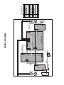
WIRING DIAGRAM
8 14Pin
6631T20033T
6631T20033A
6631T20033E
6631T20033D
7
8
9
6631T20033F
6
6631T25019K
6631T20032T
3
5
6631T20032S
2
4
6631T11020N
Part No.
1
No.
Wiring Part List
- 25 -
001
007
005
008
009
002
010
006
011
012
013
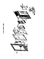
EXPLODED VIEW
003
015
014
004
016
EXPLODED VIEW PARTS LIST
DESCRIPTION
No.
PART NO.
001
3091TKE019A
CABINET ASSEMBLY, RM-32LZ50 BRAND 3090TKE014 .
3091TKE019H
CABINET ASSEMBLY, RM-32LZ50.ATPLKTA BRAND 3090TKE014 51SF
3091TKE019D
CABINET ASSEMBLY, RM-32LZ50 BRAND 3090TKE014 SKD
002
6304FLP163A
LCD(LIQUID CRYSTAL DISPLAY), LC320W01-A6 LG PHILPS TFT COLOR WXGA, 16:9, 500NITS, 16MS, 8BIT, LVDS
003
3809TKE018A
BACK COVER ASSEMBLY, RM-32LZ50 3808TKE014 .
3809TKE018J
BACK COVER ASSEMBLY, RM-32LZ50 3808TKE014 SET SOUTH AMERCIA
3809TKE018E
BACK COVER ASSEMBLY, RM-32LZ50 3808TKE014 SKD
3043TKK172C
TILT SWIVEL ASSEMBLY, RM-30LZ50 NON NON
3043TKK172A
TILT SWIVEL ASSEMBLY, RZ-30LZ50 NONE NONE
3043TKK172D
TILT SWIVEL ASSEMBLY, RM-30LZ50 NON C/SKD
005
6401TZZ042C
SPEAKER ASSEMBLY, RZ-30LZ50 5WX2EA,8OHM,ESTEC(L),5P,UL1185#24,
006
6401TZZ042D
SPEAKER ASSEMBLY, RZ-30LZ50 5WX2EA,8OHM,ESTEC(R),4P,UL1185#24
007
6871TST589A
PWB(PCB) ASSEMBLY,SUB, 26LZ50 KEY SUB TOTAL BRAND KEY BOARD
008
6871TST642B
PWB(PCB) ASSEMBLY,SUB, RM-32LZ50 LED & P/SW TOTAL BRAND .
009
6871TVT370A
PWB(PCB) ASSEMBLY,VIDEO, RZ-30LZ50 SIDE A/V SUB TOTAL BRAND .
010
4951TKS170C
METAL ASSEMBLY, FRAME 32LZ50
4951TKS170D
METAL ASSEMBLY, FRAME 32LZ50 SKD
6871TPT275A
PWB(PCB) ASSEMBLY,POWER, RZ-30LZ50 POWER TOTAL BRAND ML-041A, 23",26",27",30",32" AUTOBAN
or 6871TPT294A
PWB(PCB) ASSEMBLY,POWER, RZ/T-32LZ50 POWER TOTAL BRAND POWER BOARD FOR 32" LPL
004
011
012
3313TN3005A
MAIN TOTAL ASSEMBLY, RM-32LZ50(PREMIUM) BRAND ML-041A
013
4951TKK169M
METAL ASSEMBLY, REAR RM-32LZ50 CANADA
4951TKK169C
METAL ASSEMBLY, REAR RZ-32LZ50
014
4951TKK169F
METAL ASSEMBLY, REAR RZ-32LZ50
015
3551TKK516C
COVER ASSEMBLY, RM/RT-30LZ50 REAR NON NON
3551TKK516D
COVER ASSEMBLY, RM/RT-30LZ50 REAR NON C/SKD
3550TKK581A
COVER, RZ-32LZ50 REAR AV
3550TKK581B
COVER, RZ-32LZ50 REAR SKD
016
- 26 -
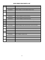
REPLACEMENT PARTS LIST
For Capacitor & Resistors, the
charactors at 2nd and 3rd digit in the
P/No. means as follows;
*S *AL LOC. NO.
PART NO.
CC, CX, CK, CN, CH : Ceramic
CQ : Polyestor
CE : Electrolytic
CF : Fixed Film
DATE: 2004. 10. 28.
DESCRIPTION / SPECIFICATION
*S *AL LOC. NO.
RD : Carbon Film
RS : Metal Oxide Film
RN : Metal Film
RH : CHIP, Metal Glazed(Chip)
RR : Drawing
PART NO.
DATE: 2004. 10. 28.
DESCRIPTION / SPECIFICATION
CAPACITOR
C108
C1100
C1102
C1112
C1113
C1114
C1115
C119
C120
C404
C1015
C1016
C13
C1303
C1308
C14
C2
C20
C237
C238
C319
C321
C324
C326
C327
C331
C333
C336
C338
C339
C43
C46
C464
C468
C50
C515
C516
C701
C702
C74
C755
C756
C757
C758
C83
C924
C925
C129
C130
C1001
C1002
C1003
C1004
C1007
0CE476EK638
0CE106BF618
0CE107CK638
0CE108EF618
0CE108EF618
0CE108EF618
0CE108EF618
0CE106BF618
0CE106BF618
0CE227EJ638
0CH6680K416
0CH6680K416
0CH6102K406
0CH6101K416
0CH6101K416
0CH6102K406
0CH6102K406
0CH6102K406
0CH6102K406
0CH6102K406
0CH6120K416
0CH6120K416
0CH6120K416
0CH6120K416
0CH6120K416
0CH6150K416
0CH6150K416
0CH6150K416
0CH6150K416
0CH6150K416
0CH6102K406
0CH6102K406
0CH6102K406
0CH6820K416
0CH6102K406
0CH6330K416
0CH6330K416
0CH6120K416
0CH6120K416
0CH6102K406
0CH6471K416
0CH6471K416
0CH6471K416
0CH6101K416
0CH6102K406
0CH6080K116
0CH6080K116
181-007F
181-007F
0CH3103K516
0CH3103K516
0CH3103K516
0CH3103K516
0CH3103K516
C1010
C1017
C1018
C107
C109
C110
C113
C114
C127
C128
C1300
C1302
C1305
C1307
C135
C136
C15
C19
C23
C3
C4
C42
C44
C450
C453
C454
C455
C456
C458
C459
C460
C461
C462
C465
C466
C467
C470
C471
C475
C479
C480
C481
C482
C483
C484
C485
C49
C500
C505
C506
C507
C508
C509
C510
47UF KMG 50V M FM5 TP 5
10UF KME 16V M FL TP5
"100UF SHL,SD 50V M FM5 TP 5"
1000UF KMG 16V M FL TP 5
1000UF KMG 16V M FL TP 5
1000UF KMG 16V M FL TP 5
1000UF KMG 16V M FL TP 5
10UF KME 16V M FL TP5
10UF KME 16V M FL TP5
220UF KMG 35V M FM5 TP 5
68PF 50V J NP0 2012 R/TP
68PF 50V J NP0 2012 R/TP
1000PF 50V J SL 2012 R/TP
100PF 50V J NP0 2012 R/TP
100PF 50V J NP0 2012 R/TP
1000PF 50V J SL 2012 R/TP
1000PF 50V J SL 2012 R/TP
1000PF 50V J SL 2012 R/TP
1000PF 50V J SL 2012 R/TP
1000PF 50V J SL 2012 R/TP
12PF 50V J NP0 2012 R/TP
12PF 50V J NP0 2012 R/TP
12PF 50V J NP0 2012 R/TP
12PF 50V J NP0 2012 R/TP
12PF 50V J NP0 2012 R/TP
15PF 50V J NP0 2012 R/TP
15PF 50V J NP0 2012 R/TP
15PF 50V J NP0 2012 R/TP
15PF 50V J NP0 2012 R/TP
15PF 50V J NP0 2012 R/TP
1000PF 50V J SL 2012 R/TP
1000PF 50V J SL 2012 R/TP
1000PF 50V J SL 2012 R/TP
82PF 50V J NP0 2012 R/TP
1000PF 50V J SL 2012 R/TP
33PF 50V J NP0 2012 R/TP
33PF 50V J NP0 2012 R/TP
12PF 50V J NP0 2012 R/TP
12PF 50V J NP0 2012 R/TP
1000PF 50V J SL 2012 R/TP
470F 50V J NP0 2012 R/TP
470F 50V J NP0 2012 R/TP
470F 50V J NP0 2012 R/TP
100PF 50V J NP0 2012 R/TP
1000PF 50V J SL 2012 R/TP
8PF 50V D NP0 2012 R/TP
8PF 50V D NP0 2012 R/TP
"MPE ECQ-V1H224JL3(TR), 50V 0."
"MPE ECQ-V1H224JL3(TR), 50V 0."
10000PF 50V 10% B(Y5P) 2012 R
10000PF 50V 10% B(Y5P) 2012 R
10000PF 50V 10% B(Y5P) 2012 R
10000PF 50V 10% B(Y5P) 2012 R
10000PF 50V 10% B(Y5P) 2012 R
- 27 -
0CK273DK51A
0CH5390K416
0CH5390K416
0CK225DFK4A
0CH3103K516
0CH3103K516
0CK225DFK4A
0CK225DFK4A
0CH3104K566
0CH3104K566
0CH3104K566
0CH3103K516
0CH3104K566
0CH3103K516
0CH3104K566
0CH3104K566
0CH3104K566
0CH3104K566
0CH3104K566
0CH3104K566
0CH3104K566
0CH3104K566
0CH3104K566
0CH3104K566
0CH3103K516
0CH3103K516
0CH3103K516
0CH3103K516
0CH3474H946
0CH3103K516
0CH3103K516
0CH3103K516
0CH3474H946
0CH3104K566
0CH3474H946
0CH6470K416
0CH3104K566
0CH3104K566
0CH3104K566
0CH3104K566
0CH3104K566
0CH3104K566
0CH3104K566
0CH3104K566
0CH3104K566
0CH3104K566
0CH3104K566
0CH3104K566
0CH3104K566
0CH3104K566
0CH3104K566
0CH3104K566
0CH3104K566
0CH3104K566
27000PF 2012 50V 10% B(Y5P) R
39PF 50V 5% NP0 2012 R/TP
39PF 50V 5% NP0 2012 R/TP
"2.2UF 2012 16V 20%,-20% F(Y5V"
10000PF 50V 10% B(Y5P) 2012 R
10000PF 50V 10% B(Y5P) 2012 R
"2.2UF 2012 16V 20%,-20% F(Y5V"
"2.2UF 2012 16V 20%,-20% F(Y5V"
0.1UF 50V 10% X7R 2012 R/TP
0.1UF 50V 10% X7R 2012 R/TP
0.1UF 50V 10% X7R 2012 R/TP
10000PF 50V 10% B(Y5P) 2012 R
0.1UF 50V 10% X7R 2012 R/TP
10000PF 50V 10% B(Y5P) 2012 R
0.1UF 50V 10% X7R 2012 R/TP
0.1UF 50V 10% X7R 2012 R/TP
0.1UF 50V 10% X7R 2012 R/TP
0.1UF 50V 10% X7R 2012 R/TP
0.1UF 50V 10% X7R 2012 R/TP
0.1UF 50V 10% X7R 2012 R/TP
0.1UF 50V 10% X7R 2012 R/TP
0.1UF 50V 10% X7R 2012 R/TP
0.1UF 50V 10% X7R 2012 R/TP
0.1UF 50V 10% X7R 2012 R/TP
10000PF 50V 10% B(Y5P) 2012 R
10000PF 50V 10% B(Y5P) 2012 R
10000PF 50V 10% B(Y5P) 2012 R
10000PF 50V 10% B(Y5P) 2012 R
"0.47UF 25V 80%,-20% F(Y5V) 20"
10000PF 50V 10% B(Y5P) 2012 R
10000PF 50V 10% B(Y5P) 2012 R
10000PF 50V 10% B(Y5P) 2012 R
"0.47UF 25V 80%,-20% F(Y5V) 20"
0.1UF 50V 10% X7R 2012 R/TP
"0.47UF 25V 80%,-20% F(Y5V) 20"
47PF 50V 5% NP0 2012 R/TP
0.1UF 50V 10% X7R 2012 R/TP
0.1UF 50V 10% X7R 2012 R/TP
0.1UF 50V 10% X7R 2012 R/TP
0.1UF 50V 10% X7R 2012 R/TP
0.1UF 50V 10% X7R 2012 R/TP
0.1UF 50V 10% X7R 2012 R/TP
0.1UF 50V 10% X7R 2012 R/TP
0.1UF 50V 10% X7R 2012 R/TP
0.1UF 50V 10% X7R 2012 R/TP
0.1UF 50V 10% X7R 2012 R/TP
0.1UF 50V 10% X7R 2012 R/TP
0.1UF 50V 10% X7R 2012 R/TP
0.1UF 50V 10% X7R 2012 R/TP
0.1UF 50V 10% X7R 2012 R/TP
0.1UF 50V 10% X7R 2012 R/TP
0.1UF 50V 10% X7R 2012 R/TP
0.1UF 50V 10% X7R 2012 R/TP
0.1UF 50V 10% X7R 2012 R/TP
*S *AL LOC. NO.
C511
C512
C513
C514
C517
C518
C519
C521
C522
C523
C526
C527
C528
C529
C530
C531
C532
C533
C534
C535
C536
C537
C538
C539
C540
C541
C542
C544
C545
C546
C547
C549
C550
C551
C552
C553
C554
C555
C556
C557
C558
C559
C567
C6
C60
C606
C608
C609
C614
C615
C616
C618
C619
C620
C621
C622
C623
C624
C625
C627
C628
C629
PART NO.
0CH3104K566
0CH3104K566
0CH3104K566
0CH3104K566
0CH3104K566
0CH3104K566
0CH3104K566
0CH3104K566
0CH3104K566
0CH3104K566
0CH3104K566
0CH3104K566
0CH3104K566
0CH3104K566
0CH3104K566
0CH3104K566
0CH3104K566
0CH3104K566
0CH3104K566
0CH3104K566
0CH3104K566
0CH3104K566
0CH3104K566
0CH3104K566
0CH3104K566
0CH3104K566
0CH3104K566
0CH3104K566
0CH3104K566
0CH3104K566
0CH3104K566
0CH3104K566
0CH3104K566
0CH3104K566
0CH3104K566
0CH3104K566
0CH3104K566
0CH3104K566
0CH3104K566
0CH3104K566
0CH3104K566
0CH3104K566
0CH3104K566
0CH3104K566
0CH3104K566
0CH3104K566
0CH3104K566
0CH3104K566
0CH3104K566
0CH3104K566
0CH3104K566
0CH3104K566
0CH3104K566
0CH3104K566
0CH3104K566
0CH3104K566
0CH3104K566
0CH3104K566
0CH3104K566
0CH3104K566
0CH3822K516
0CH3823K516
DATE: 2004. 10. 28.
DESCRIPTION / SPECIFICATION
*S *AL LOC. NO.
0.1UF 50V 10% X7R 2012 R/TP
0.1UF 50V 10% X7R 2012 R/TP
0.1UF 50V 10% X7R 2012 R/TP
0.1UF 50V 10% X7R 2012 R/TP
0.1UF 50V 10% X7R 2012 R/TP
0.1UF 50V 10% X7R 2012 R/TP
0.1UF 50V 10% X7R 2012 R/TP
0.1UF 50V 10% X7R 2012 R/TP
0.1UF 50V 10% X7R 2012 R/TP
0.1UF 50V 10% X7R 2012 R/TP
0.1UF 50V 10% X7R 2012 R/TP
0.1UF 50V 10% X7R 2012 R/TP
0.1UF 50V 10% X7R 2012 R/TP
0.1UF 50V 10% X7R 2012 R/TP
0.1UF 50V 10% X7R 2012 R/TP
0.1UF 50V 10% X7R 2012 R/TP
0.1UF 50V 10% X7R 2012 R/TP
0.1UF 50V 10% X7R 2012 R/TP
0.1UF 50V 10% X7R 2012 R/TP
0.1UF 50V 10% X7R 2012 R/TP
0.1UF 50V 10% X7R 2012 R/TP
0.1UF 50V 10% X7R 2012 R/TP
0.1UF 50V 10% X7R 2012 R/TP
0.1UF 50V 10% X7R 2012 R/TP
0.1UF 50V 10% X7R 2012 R/TP
0.1UF 50V 10% X7R 2012 R/TP
0.1UF 50V 10% X7R 2012 R/TP
0.1UF 50V 10% X7R 2012 R/TP
0.1UF 50V 10% X7R 2012 R/TP
0.1UF 50V 10% X7R 2012 R/TP
0.1UF 50V 10% X7R 2012 R/TP
0.1UF 50V 10% X7R 2012 R/TP
0.1UF 50V 10% X7R 2012 R/TP
0.1UF 50V 10% X7R 2012 R/TP
0.1UF 50V 10% X7R 2012 R/TP
0.1UF 50V 10% X7R 2012 R/TP
0.1UF 50V 10% X7R 2012 R/TP
0.1UF 50V 10% X7R 2012 R/TP
0.1UF 50V 10% X7R 2012 R/TP
0.1UF 50V 10% X7R 2012 R/TP
0.1UF 50V 10% X7R 2012 R/TP
0.1UF 50V 10% X7R 2012 R/TP
0.1UF 50V 10% X7R 2012 R/TP
0.1UF 50V 10% X7R 2012 R/TP
0.1UF 50V 10% X7R 2012 R/TP
0.1UF 50V 10% X7R 2012 R/TP
0.1UF 50V 10% X7R 2012 R/TP
0.1UF 50V 10% X7R 2012 R/TP
0.1UF 50V 10% X7R 2012 R/TP
0.1UF 50V 10% X7R 2012 R/TP
0.1UF 50V 10% X7R 2012 R/TP
0.1UF 50V 10% X7R 2012 R/TP
0.1UF 50V 10% X7R 2012 R/TP
0.1UF 50V 10% X7R 2012 R/TP
0.1UF 50V 10% X7R 2012 R/TP
0.1UF 50V 10% X7R 2012 R/TP
0.1UF 50V 10% X7R 2012 R/TP
0.1UF 50V 10% X7R 2012 R/TP
0.1UF 50V 10% X7R 2012 R/TP
0.1UF 50V 10% X7R 2012 R/TP
8200PF 2012 50V 10% B(Y5P) R/
82000PF 2012 50V 10% B(Y5P) R
C632
C633
C634
C635
C636
C637
C638
C639
C64
C640
C700
C704
C705
C75
C751
C76
C760
C761
C77
C79
C80
C804
C808
C809
C81
C810
C811
C812
C813
C82
C84
C850
C851
C852
C853
C854
C855
C856
C864
C865
C866
C867
C868
C869
C870
C908
C909
C910
C911
C912
C913
C914
C915
C916
C917
C918
C919
C920
C921
C922
C923
C926
- 28 -
PART NO.
0CH3104K566
0CH3104K566
0CH3104K566
0CH3104K566
0CH3104K566
0CH3104K566
0CH3104K566
0CH3104K566
0CH3104K566
0CH3104K566
0CH3104K566
0CH3104K566
0CH3104K566
0CH3104K566
0CH3104K566
0CK106EF56A
0CH3104K566
0CH3104K566
0CK106EF56A
0CK106EF56A
0CK106EF56A
0CH3104K566
0CK105DK94A
0CK105DK94A
0CK106EF56A
0CH3104K566
0CH3104K566
0CH3104K566
0CH3104K566
0CH3104K566
0CK106EF56A
0CH3104K566
0CH3104K566
0CH3104K566
0CH3104K566
0CH3104K566
0CH3104K566
0CH3104K566
0CH3104K566
0CH3104K566
0CH3104K566
0CH3104K566
0CH3104K566
0CH3104K566
0CH3104K566
0CH3104K566
0CH3104K566
0CH3104K566
0CH3104K566
0CH3104K566
0CH3104K566
0CH3104K566
0CH3104K566
0CH3104K566
0CH3104K566
0CH3104K566
0CH3104K566
0CH3104K566
0CH3104K566
0CH3104K566
0CH3104K566
0CH3104K566
DATE: 2004. 10. 28.
DESCRIPTION / SPECIFICATION
0.1UF 50V 10% X7R 2012 R/TP
0.1UF 50V 10% X7R 2012 R/TP
0.1UF 50V 10% X7R 2012 R/TP
0.1UF 50V 10% X7R 2012 R/TP
0.1UF 50V 10% X7R 2012 R/TP
0.1UF 50V 10% X7R 2012 R/TP
0.1UF 50V 10% X7R 2012 R/TP
0.1UF 50V 10% X7R 2012 R/TP
0.1UF 50V 10% X7R 2012 R/TP
0.1UF 50V 10% X7R 2012 R/TP
0.1UF 50V 10% X7R 2012 R/TP
0.1UF 50V 10% X7R 2012 R/TP
0.1UF 50V 10% X7R 2012 R/TP
0.1UF 50V 10% X7R 2012 R/TP
0.1UF 50V 10% X7R 2012 R/TP
10UF 3216 16V 10% X7R R/TP
0.1UF 50V 10% X7R 2012 R/TP
0.1UF 50V 10% X7R 2012 R/TP
10UF 3216 16V 10% X7R R/TP
10UF 3216 16V 10% X7R R/TP
10UF 3216 16V 10% X7R R/TP
0.1UF 50V 10% X7R 2012 R/TP
"1UF 2012 50V 80%,-20% R/TP F("
"1UF 2012 50V 80%,-20% R/TP F("
10UF 3216 16V 10% X7R R/TP
0.1UF 50V 10% X7R 2012 R/TP
0.1UF 50V 10% X7R 2012 R/TP
0.1UF 50V 10% X7R 2012 R/TP
0.1UF 50V 10% X7R 2012 R/TP
0.1UF 50V 10% X7R 2012 R/TP
10UF 3216 16V 10% X7R R/TP
0.1UF 50V 10% X7R 2012 R/TP
0.1UF 50V 10% X7R 2012 R/TP
0.1UF 50V 10% X7R 2012 R/TP
0.1UF 50V 10% X7R 2012 R/TP
0.1UF 50V 10% X7R 2012 R/TP
0.1UF 50V 10% X7R 2012 R/TP
0.1UF 50V 10% X7R 2012 R/TP
0.1UF 50V 10% X7R 2012 R/TP
0.1UF 50V 10% X7R 2012 R/TP
0.1UF 50V 10% X7R 2012 R/TP
0.1UF 50V 10% X7R 2012 R/TP
0.1UF 50V 10% X7R 2012 R/TP
0.1UF 50V 10% X7R 2012 R/TP
0.1UF 50V 10% X7R 2012 R/TP
0.1UF 50V 10% X7R 2012 R/TP
0.1UF 50V 10% X7R 2012 R/TP
0.1UF 50V 10% X7R 2012 R/TP
0.1UF 50V 10% X7R 2012 R/TP
0.1UF 50V 10% X7R 2012 R/TP
0.1UF 50V 10% X7R 2012 R/TP
0.1UF 50V 10% X7R 2012 R/TP
0.1UF 50V 10% X7R 2012 R/TP
0.1UF 50V 10% X7R 2012 R/TP
0.1UF 50V 10% X7R 2012 R/TP
0.1UF 50V 10% X7R 2012 R/TP
0.1UF 50V 10% X7R 2012 R/TP
0.1UF 50V 10% X7R 2012 R/TP
0.1UF 50V 10% X7R 2012 R/TP
0.1UF 50V 10% X7R 2012 R/TP
0.1UF 50V 10% X7R 2012 R/TP
0.1UF 50V 10% X7R 2012 R/TP
*S *AL LOC. NO.
C927
C928
C929
C930
C931
C935
C936
C938
C939
C940
C941
C942
C943
C944
C945
C946
C947
C948
C949
C950
C951
C952
C958
C960
C963
C969
C970
C973
C98
C99
C10
C11
C115
C116
C117
C118
C12
C125
C126
C1301
C1306
C16
C18
C25
C26
C27
C28
C29
C30
C306
C31
C318
C32
C33
C34
C35
C36
C37
C38
C39
C40
C41
PART NO.
0CH3104K566
0CH3104K566
0CH3104K566
0CH3104K566
0CH3104K566
0CH3104K566
0CH3104K566
0CH3104K566
0CH3104K566
0CH3104K566
0CH3104K566
0CH3104K566
0CH3104K566
0CH3104K566
0CH3104K566
0CH3104K566
0CH3104K566
0CH3104K566
0CH3104K566
0CH3104K566
0CH3104K566
0CH3104K566
0CK225DFK4A
0CH3104K566
0CH3104K566
0CH3104K566
0CH3104K566
0CH3104K566
0CH5390K416
0CH5390K416
0CK104CK56A
0CK104CK56A
0CK104CK56A
0CK562CK51A
0CK562CK51A
0CK104CK56A
0CK104CK56A
0CK105EK56A
0CK105EK56A
0CK103CK51A
0CK103CK51A
0CK104CK56A
0CK106EF56A
0CK104CK56A
0CK104CK56A
0CK104CK56A
0CK334CF94A
0CK104CK56A
0CK334CF94A
0CK104CK56A
0CK104CK56A
0CK104CK56A
0CK334CF94A
0CK334CF94A
0CK104CK56A
0CK334CF94A
0CK104CK56A
0CK334CF94A
0CK104CK56A
0CK104CK56A
0CK104CK56A
0CK104CK56A
DATE: 2004. 10. 28.
DESCRIPTION / SPECIFICATION
*S *AL LOC. NO.
0.1UF 50V 10% X7R 2012 R/TP
0.1UF 50V 10% X7R 2012 R/TP
0.1UF 50V 10% X7R 2012 R/TP
0.1UF 50V 10% X7R 2012 R/TP
0.1UF 50V 10% X7R 2012 R/TP
0.1UF 50V 10% X7R 2012 R/TP
0.1UF 50V 10% X7R 2012 R/TP
0.1UF 50V 10% X7R 2012 R/TP
0.1UF 50V 10% X7R 2012 R/TP
0.1UF 50V 10% X7R 2012 R/TP
0.1UF 50V 10% X7R 2012 R/TP
0.1UF 50V 10% X7R 2012 R/TP
0.1UF 50V 10% X7R 2012 R/TP
0.1UF 50V 10% X7R 2012 R/TP
0.1UF 50V 10% X7R 2012 R/TP
0.1UF 50V 10% X7R 2012 R/TP
0.1UF 50V 10% X7R 2012 R/TP
0.1UF 50V 10% X7R 2012 R/TP
0.1UF 50V 10% X7R 2012 R/TP
0.1UF 50V 10% X7R 2012 R/TP
0.1UF 50V 10% X7R 2012 R/TP
0.1UF 50V 10% X7R 2012 R/TP
"2.2UF 2012 16V 20%,-20% F(Y5V"
0.1UF 50V 10% X7R 2012 R/TP
0.1UF 50V 10% X7R 2012 R/TP
0.1UF 50V 10% X7R 2012 R/TP
0.1UF 50V 10% X7R 2012 R/TP
0.1UF 50V 10% X7R 2012 R/TP
39PF 50V 5% NP0 2012 R/TP
39PF 50V 5% NP0 2012 R/TP
0.1UF 1608 50V 10% R/TP X7R
0.1UF 1608 50V 10% R/TP X7R
0.1UF 1608 50V 10% R/TP X7R
5600PF 1608 50V 10% R/TP B(Y5
5600PF 1608 50V 10% R/TP B(Y5
0.1UF 1608 50V 10% R/TP X7R
0.1UF 1608 50V 10% R/TP X7R
1UF 3216 50V 10% X7R R/TP
1UF 3216 50V 10% X7R R/TP
0.01UF 1608 50V 10% R/TP B(Y5
0.01UF 1608 50V 10% R/TP B(Y5
0.1UF 1608 50V 10% R/TP X7R
10UF 3216 16V 10% X7R R/TP
0.1UF 1608 50V 10% R/TP X7R
0.1UF 1608 50V 10% R/TP X7R
0.1UF 1608 50V 10% R/TP X7R
"0.33UF 1608 16V 80%,-20% F(Y5"
0.1UF 1608 50V 10% R/TP X7R
"0.33UF 1608 16V 80%,-20% F(Y5"
0.1UF 1608 50V 10% R/TP X7R
0.1UF 1608 50V 10% R/TP X7R
0.1UF 1608 50V 10% R/TP X7R
"0.33UF 1608 16V 80%,-20% F(Y5"
"0.33UF 1608 16V 80%,-20% F(Y5"
0.1UF 1608 50V 10% R/TP X7R
"0.33UF 1608 16V 80%,-20% F(Y5"
0.1UF 1608 50V 10% R/TP X7R
"0.33UF 1608 16V 80%,-20% F(Y5"
0.1UF 1608 50V 10% R/TP X7R
0.1UF 1608 50V 10% R/TP X7R
0.1UF 1608 50V 10% R/TP X7R
0.1UF 1608 50V 10% R/TP X7R
C45
C463
C469
C473
C476
C477
C478
C486
C487
C488
C5001
C504
C51
C524
C61
C611
C612
C613
C626
C65
C66
C67
C70
C71
C72
C73
C750
C752
C753
C759
C78
C800
C801
C802
C803
C90
C901
C902
C903
C904
C905
C906
C907
C91
C96
C121
C122
C21
C22
C24
C328
C340
C343
C345
C348
C350
C351
C352
C47
C474
C48
C501
- 29 -
PART NO.
0CK104CK56A
0CK103CK51A
0CK152CK51A
0CK474CH94A
0CK103CK51A
0CK103CK51A
0CK103CK51A
0CK103CK51A
0CK474CH94A
0CK474CH94A
0CK104CK56A
0CK104CK56A
0CK104CK56A
0CK104CK56A
0CK104CK56A
0CK473CK56A
0CK473CK56A
0CK473CK56A
0CK104CK56A
0CK104CK56A
0CK106EF56A
0CK104CK56A
0CK104CK56A
0CK106EF56A
0CK106EF56A
0CK106EF56A
0CK104CK56A
0CK104CK56A
0CK104CK56A
0CK104CK56A
0CK106EF56A
0CK105CF94A
0CK105CF94A
0CK105CF94A
0CK105CF94A
0CK104CK56A
0CK103CK51A
0CK103CK51A
0CK103CK51A
0CK103CK51A
0CK103CK51A
0CK103CK51A
0CK103CK51A
0CK104CK56A
0CK104CK56A
0CC100CK41A
0CC100CK41A
0CC102CK41A
0CC102CK41A
0CC102CK41A
0CC120CK41A
0CC150CK41A
0CC270CK41A
0CC270CK41A
0CC270CK41A
0CC270CK41A
0CC270CK41A
0CC270CK41A
0CC220CK41A
0CC330CK41A
0CC220CK41A
0CC101CK41A
DATE: 2004. 10. 28.
DESCRIPTION / SPECIFICATION
0.1UF 1608 50V 10% R/TP X7R
0.01UF 1608 50V 10% R/TP B(Y5
1500PF 1608 50V 10% R/TP B(Y5
"0.47UF 1608 25V 80%,-20% R/TP"
0.01UF 1608 50V 10% R/TP B(Y5
0.01UF 1608 50V 10% R/TP B(Y5
0.01UF 1608 50V 10% R/TP B(Y5
0.01UF 1608 50V 10% R/TP B(Y5
"0.47UF 1608 25V 80%,-20% R/TP"
"0.47UF 1608 25V 80%,-20% R/TP"
0.1UF 1608 50V 10% R/TP X7R
0.1UF 1608 50V 10% R/TP X7R
0.1UF 1608 50V 10% R/TP X7R
0.1UF 1608 50V 10% R/TP X7R
0.1UF 1608 50V 10% R/TP X7R
47000PF 1608 50V 10% R/TP X7R
47000PF 1608 50V 10% R/TP X7R
47000PF 1608 50V 10% R/TP X7R
0.1UF 1608 50V 10% R/TP X7R
0.1UF 1608 50V 10% R/TP X7R
10UF 3216 16V 10% X7R R/TP
0.1UF 1608 50V 10% R/TP X7R
0.1UF 1608 50V 10% R/TP X7R
10UF 3216 16V 10% X7R R/TP
10UF 3216 16V 10% X7R R/TP
10UF 3216 16V 10% X7R R/TP
0.1UF 1608 50V 10% R/TP X7R
0.1UF 1608 50V 10% R/TP X7R
0.1UF 1608 50V 10% R/TP X7R
0.1UF 1608 50V 10% R/TP X7R
10UF 3216 16V 10% X7R R/TP
"1UF 1608 16V 80%,-20% R/TP F("
"1UF 1608 16V 80%,-20% R/TP F("
"1UF 1608 16V 80%,-20% R/TP F("
"1UF 1608 16V 80%,-20% R/TP F("
0.1UF 1608 50V 10% R/TP X7R
0.01UF 1608 50V 10% R/TP B(Y5
0.01UF 1608 50V 10% R/TP B(Y5
0.01UF 1608 50V 10% R/TP B(Y5
0.01UF 1608 50V 10% R/TP B(Y5
0.01UF 1608 50V 10% R/TP B(Y5
0.01UF 1608 50V 10% R/TP B(Y5
0.01UF 1608 50V 10% R/TP B(Y5
0.1UF 1608 50V 10% R/TP X7R
0.1UF 1608 50V 10% R/TP X7R
10PF 1608 50V 5% R/TP NP0
10PF 1608 50V 5% R/TP NP0
1000PF 1608 50V 5% R/TP NP0
1000PF 1608 50V 5% R/TP NP0
1000PF 1608 50V 5% R/TP NP0
12PF 1608 50V 5% R/TP NP0
15PF 1608 50V 5% R/TP NP0
27PF 1608 50V 5% R/TP NP0
27PF 1608 50V 5% R/TP NP0
27PF 1608 50V 5% R/TP NP0
27PF 1608 50V 5% R/TP NP0
27PF 1608 50V 5% R/TP NP0
27PF 1608 50V 5% R/TP NP0
22PF 1608 50V 5% R/TP NP0
33PF 1608 50V 5% R/TP NP0
22PF 1608 50V 5% R/TP NP0
100PF 1608 50V 5% R/TP NP0
*S *AL LOC. NO.
C53
C59
C600
C601
C602
C603
C610
C754
C85
C86
C111
C112
C1202
C123
C124
C1299
C1304
C131
C132
C133
C134
C100
C1006
C1008
C17
C212
C213
C216
C225
C226
C227
C228
C307
C308
C309
C312
C313
C314
C315
C316
C451
C457
C5
C502
C503
C52
C520
C525
C54
C543
C55
C560
C566
C604
C605
C607
C62
C63
C703
C805
C806
C807
PART NO.
0CC102CK41A
0CC102CK41A
0CC220CK41A
0CC220CK41A
0CC220CK41A
0CC220CK41A
0CC102CK41A
0CC471CK41A
0CC102CK41A
0CC102CK41A
0CE475EK638
0CE475EK638
0CE477EJ618
0CE477EJ618
0CE477EJ618
0CE477EJ618
0CE477EJ618
0CE477EJ618
0CE477EJ618
0CE477EJ618
0CE477EJ618
0CH8476F691
0CH8106J691
0CE227WF6DC
0CH8106J691
0CH8106F691
0CH8106F691
0CH8106F691
0CH8106J691
0CH8106J691
0CH8106J691
0CH8106J691
0CH8106F691
0CH8476H691
0CH8106F691
0CH8106F691
0CH8476H691
0CH8106F691
0CH8106F691
0CH8106F691
0CH8476F691
0CH8476F691
0CE475WJ6DC
0CH8476F691
0CH8476F691
0CH8476F691
0CH8106F691
0CH8106F691
0CH8476F691
0CH8476F691
0CH8476H691
0CH8476F691
0CH8476F691
0CH8476F691
0CH8476F691
0CH8476F691
0CH8476F691
0CH8476F691
0CE107WF6DC
0CE227WF6DC
0CE227WF6DC
0CE227WF6DC
DATE: 2004. 10. 28.
DESCRIPTION / SPECIFICATION
*S *AL LOC. NO.
1000PF 1608 50V 5% R/TP NP0
1000PF 1608 50V 5% R/TP NP0
22PF 1608 50V 5% R/TP NP0
22PF 1608 50V 5% R/TP NP0
22PF 1608 50V 5% R/TP NP0
22PF 1608 50V 5% R/TP NP0
1000PF 1608 50V 5% R/TP NP0
470PF 1608 50V 5% R/TP NP0
1000PF 1608 50V 5% R/TP NP0
1000PF 1608 50V 5% R/TP NP0
4.7UF KMG 50V 20% FM5 TP 5
4.7UF KMG 50V 20% FM5 TP 5
470UF KMG 35V 20% FL TP 5
470UF KMG 35V 20% FL TP 5
470UF KMG 35V 20% FL TP 5
470UF KMG 35V 20% FL TP 5
470UF KMG 35V 20% FL TP 5
470UF KMG 35V 20% FL TP 5
470UF KMG 35V 20% FL TP 5
470UF KMG 35V 20% FL TP 5
470UF KMG 35V 20% FL TP 5
47UF 16V 20% 105STD (CYL) R/T
10UF 35V 20% 105STD (CYL) R/T
220UF MVK 16V 20% R/TP(SMD) S
10UF 35V 20% 105STD (CYL) R/T
10UF 16V 20% 105STD (CYL) R/T
10UF 16V 20% 105STD (CYL) R/T
10UF 16V 20% 105STD (CYL) R/T
10UF 35V 20% 105STD (CYL) R/T
10UF 35V 20% 105STD (CYL) R/T
10UF 35V 20% 105STD (CYL) R/T
10UF 35V 20% 105STD (CYL) R/T
10UF 16V 20% 105STD (CYL) R/T
47UF 25V 20% 105STD (CYL) R/T
10UF 16V 20% 105STD (CYL) R/T
10UF 16V 20% 105STD (CYL) R/T
47UF 25V 20% 105STD (CYL) R/T
10UF 16V 20% 105STD (CYL) R/T
10UF 16V 20% 105STD (CYL) R/T
10UF 16V 20% 105STD (CYL) R/T
47UF 16V 20% 105STD (CYL) R/T
47UF 16V 20% 105STD (CYL) R/T
4.7UF MVK 35V 20% R/TP(SMD) S
47UF 16V 20% 105STD (CYL) R/T
47UF 16V 20% 105STD (CYL) R/T
47UF 16V 20% 105STD (CYL) R/T
10UF 16V 20% 105STD (CYL) R/T
10UF 16V 20% 105STD (CYL) R/T
47UF 16V 20% 105STD (CYL) R/T
47UF 16V 20% 105STD (CYL) R/T
47UF 25V 20% 105STD (CYL) R/T
47UF 16V 20% 105STD (CYL) R/T
47UF 16V 20% 105STD (CYL) R/T
47UF 16V 20% 105STD (CYL) R/T
47UF 16V 20% 105STD (CYL) R/T
47UF 16V 20% 105STD (CYL) R/T
47UF 16V 20% 105STD (CYL) R/T
47UF 16V 20% 105STD (CYL) R/T
100UF MVK 16V 20% R/TP(SMD) S
220UF MVK 16V 20% R/TP(SMD) S
220UF MVK 16V 20% R/TP(SMD) S
220UF MVK 16V 20% R/TP(SMD) S
C814
C815
C857
C858
C859
C860
C861
C862
C863
C87
C88
C89
C900
C953
C956
C957
C959
C97
C972
PART NO.
DATE: 2004. 10. 28.
DESCRIPTION / SPECIFICATION
0CE227WF6DC
0CH8476F691
0CE227WF6DC
0CH8476F691
0CH8476F691
0CH8476F691
0CH8476F691
0CH8476F691
0CH8476F691
0CH8476F691
0CH8476H691
0CH8476F691
0CH8476F691
0CH8476F691
0CH8476H691
0CH8476F691
0CH8476F691
0CH8476H691
0CH8476H691
220UF MVK 16V 20% R/TP(SMD) S
47UF 16V 20% 105STD (CYL) R/T
220UF MVK 16V 20% R/TP(SMD) S
47UF 16V 20% 105STD (CYL) R/T
47UF 16V 20% 105STD (CYL) R/T
47UF 16V 20% 105STD (CYL) R/T
47UF 16V 20% 105STD (CYL) R/T
47UF 16V 20% 105STD (CYL) R/T
47UF 16V 20% 105STD (CYL) R/T
47UF 16V 20% 105STD (CYL) R/T
47UF 25V 20% 105STD (CYL) R/T
47UF 16V 20% 105STD (CYL) R/T
47UF 16V 20% 105STD (CYL) R/T
47UF 16V 20% 105STD (CYL) R/T
47UF 25V 20% 105STD (CYL) R/T
47UF 16V 20% 105STD (CYL) R/T
47UF 16V 20% 105STD (CYL) R/T
47UF 25V 20% 105STD (CYL) R/T
47UF 25V 20% 105STD (CYL) R/T
D100
D101
IC751
IC754
ZD1300
ZD1301
D107
D711
D102
D103
D472
D104
D105
D703
D704
ZD101
ZD222
D700
D701
D702
D705
D706
ZD5001
ZD5002
ZD5003
ZD851
ZD852
ZD1000
0DRFC00288A
0DRFC00288A
0DRSE00018A
0DRSE00018A
0DR340009AA
0DR340009AA
0DD226239AA
0DD184009AA
0DD181009AB
0DD181009AB
0DVTB00048A
0DZ620009HB
0DZ620009HB
0DZ510009EE
0DZ510009EE
0DZ510009EE
0DZ510009EE
0DZ510009EE
0DZ510009EE
0DZ510009EE
0DZ510009EE
0DZ510009EE
0DZ510009EE
0DZ510009EE
0DZ510009EE
0DZ510009EE
0DZ510009EE
0DZ330009DF
SS14 FAIR CHILD R/TP SMA 20-1
SS14 FAIR CHILD R/TP SMA 20-1
SRV05-4.TC SEMTECH R/TP SOT23
SRV05-4.TC SEMTECH R/TP SOT23
MBRS340 TP FAIRCHILD NON 40V
MBRS340 TP FAIRCHILD NON 40V
KDS226 TP KEC - - - - - KDS184 TP KEC - 85V - - - 300
KDS181 TP KEC - 85V - - - 300
KDS181 TP KEC - 85V - - - 300
1SV324E TOSHIBA R/TP 1-1E1A 4
UDZ S 6.2B TP ROHM SOD323 200
UDZ S 6.2B TP ROHM SOD323 200
UDZ S 5.1B TP ROHM-K SOD323 2
UDZ S 5.1B TP ROHM-K SOD323 2
UDZ S 5.1B TP ROHM-K SOD323 2
UDZ S 5.1B TP ROHM-K SOD323 2
UDZ S 5.1B TP ROHM-K SOD323 2
UDZ S 5.1B TP ROHM-K SOD323 2
UDZ S 5.1B TP ROHM-K SOD323 2
UDZ S 5.1B TP ROHM-K SOD323 2
UDZ S 5.1B TP ROHM-K SOD323 2
UDZ S 5.1B TP ROHM-K SOD323 2
UDZ S 5.1B TP ROHM-K SOD323 2
UDZ S 5.1B TP ROHM-K SOD323 2
UDZ S 5.1B TP ROHM-K SOD323 2
UDZ S 5.1B TP ROHM-K SOD323 2
MTZJ33B TP ROHM-K DO34 0.5W 3
IC3
IC200
IC501
IC749
IC753
IC907
IC918
IC100
IC101
0IKE702700D
0ISA722200A
0IMMREB010A
0IMMRSG036A
0IMMRSG036A
0IMCRAL006A
0IMCRAL006A
0IMCRMZ002A
0IMCRMZ002A
"KIA7027AF 3, SOT-89 TP RESET"
LA7222 (1280 AUDIO) - - - "M12L64322A-6T ESMT 86P,TSOP T"
"M24C02-WMN6T SGS-THOMSON 8P,S"
"M24C02-WMN6T SGS-THOMSON 8P,S"
AT24C16AN-10SI-2.7 ATMEL 8P S
AT24C16AN-10SI-2.7 ATMEL 8P S
MP7720 MONOLITHIC POWER SYSTE
MP7720 MONOLITHIC POWER SYSTE
DIODEs
IC
- 30 -
*S *AL LOC. NO.
IC1300
IC1301
IC500
IC750
IC850
IC2000
IC702
IC1
IC450
IC600
IC800
IC901
IC103
IC2
IC300
IC4
IC5
IC505
IC6
IC601
IC604
IC8
IC905
IC906
IC752
PART NO.
DATE: 2004. 10. 28.
DESCRIPTION / SPECIFICATION
0IMCRMZ001A
0IMCRMZ001A
0IMCRGN002C
0IMCRSG010A
0IMCRMI006A
0IMO140662A
0IMO140662A
0IPRPMN003C
0IPRPTO022A
0IPRPM3002B
0IPRPNP001A
0IPRPGN014A
0IMCRFA009A
0IPMGFA061A
0IPMGKE039A
0IPMGNS001E
0IPMGNS001D
0IPMGSG018D
0IPMGSG018D
0IPMGNS001E
0IPMGFA061A
0IMCRFA015A
0IPMGFA061A
0IPMGSG018D
0IMCRTI001A
MP1583DN MONOLITHIC POWER SYS
MP1583DN MONOLITHIC POWER SYS
FLI2300BD GENESIS 208P PQFP T
ST3232CDR SGS-THOMSON SOP16 R
"M52758FP MITSUBISHI 36PIN, R/"
"MC14066BDR2 14P,SOIC TP BILAT"
"MC14066BDR2 14P,SOIC TP BILAT"
VCT49XYF C7(NTSC+PAL) MICRONA
"TC90A65F TOSHIBA 100P,QFP TRA"
"MST9883C-110 MSTAR 80P,LQFP T"
"SM5301BS(ATSC DTV) NPC 28P,HS"
GM5221H(HDCP) GENESIS 208P QF
"KA78M08RTM, FAIRCHILD 2P D-PA"
"FAN1587AD33X FAIRCHILD 3P,DPA"
"KIA78D09F KEC 3P,DPAK R/TP 9V"
LM1117MPX-3.3 NATIONAL SEMICO
LM1117MPX-2.5 NATIONAL SEMICO
"LD1086DT18TR SGS-THOMSON 3P,D"
"LD1086DT18TR SGS-THOMSON 3P,D"
LM1117MPX-3.3 NATIONAL SEMICO
"FAN1587AD33X FAIRCHILD 3P,DPA"
KA7805R FAIRCHILD 2P D-PAK R/
"FAN1587AD33X FAIRCHILD 3P,DPA"
"LD1086DT18TR SGS-THOMSON 3P,D"
SN74HCT157D TEXAS INSTRUMENT
*S *AL LOC. NO.
L401
L5
L5000
L603
L1001
L11
L13
L14
L15
L7
L1
L10
L12
L16
L17
L2
L306
L307
L308
L309
L310
L402
L8
L9
PART NO.
6210TCE001G
6210TCE001G
6210TCE001G
6210TCE001A
0LC1020101A
0LC1032101A
0LC1032101A
0LC1032101A
0LC1032101A
0LC1032101A
0LC1032101A
0LC1032101A
0LC1032101A
0LC1032101A
0LC1032101A
0LC1032101A
0LC1532101A
0LC1532101A
0LC1532101A
0LC1532101A
0LC1532101A
0LC1532101A
0LC1032101A
0LC1032101A
DATE: 2004. 10. 28.
DESCRIPTION / SPECIFICATION
HH-1M3216-501 CERATEC 3216MM
HH-1M3216-501 CERATEC 3216MM
HH-1M3216-501 CERATEC 3216MM
HB-1S2012-080JT CERATEC 2012M
1UH 10% 2012 R/TC FI-B2012-10
10UH 10% 3216 R/TC FI-C3216-1
10UH 10% 3216 R/TC FI-C3216-1
10UH 10% 3216 R/TC FI-C3216-1
10UH 10% 3216 R/TC FI-C3216-1
10UH 10% 3216 R/TC FI-C3216-1
10UH 10% 3216 R/TC FI-C3216-1
10UH 10% 3216 R/TC FI-C3216-1
10UH 10% 3216 R/TC FI-C3216-1
10UH 10% 3216 R/TC FI-C3216-1
10UH 10% 3216 R/TC FI-C3216-1
10UH 10% 3216 R/TC FI-C3216-1
15UH 10% 3216 R/TC FI-C3216-1
15UH 10% 3216 R/TC FI-C3216-1
15UH 10% 3216 R/TC FI-C3216-1
15UH 10% 3216 R/TC FI-C3216-1
15UH 10% 3216 R/TC FI-C3216-1
15UH 10% 3216 R/TC FI-C3216-1
10UH 10% 3216 R/TC FI-C3216-1
10UH 10% 3216 R/TC FI-C3216-1
FET & TRANSISTOR
COIL & CORE & INDUCTOR
L104
L105
L1300
L1301
L100
L1002
L207
L208
L301
L302
L311
L4
L500
L501
L502
L503
L504
L505
L600
L601
L602
L701
L800
L850
L900
L901
L902
L903
L907
L202
L203
L211
L212
L3
6140TBZ045A
6140TBZ045A
6140VR0008B
6140VR0008B
6210TCE001G
6210TCE001G
6210TCE001A
6210TCE001A
6210TCE001A
6210TCE001A
6210TCE001G
6210TCE001G
6210TCE001G
6210TCE001G
6210TCE001G
6210TCE001G
6210TCE001G
6210TCE001G
6210TCE001G
6210TCE001G
6210TCE001G
6210TCE001G
6210TCE001G
6210TCE001G
6210TCE001G
6210TCE001G
6210TCE001G
6210TCE001G
6210TCE001G
6210TCE001A
6210TCE001A
6210TCE001A
6210TCE001A
6210TCE001G
IC1101
IC902
Q1000
Q1101
Q211
Q212
Q213
Q451
Q701
Q100
Q101
Q12
Q13
Q14
Q15
Q210
Q308
Q310
Q313
Q315
Q316
Q317
Q450
Q454
Q500
Q901
"38.5UH(DIP), 6A, P7.5, DR8.3X"
"38.5UH(DIP), 6A, P7.5, DR8.3X"
SLF12575T-150M3R2 15UH SMD C
SLF12575T-150M3R2 15UH SMD C
HH-1M3216-501 CERATEC 3216MM
HH-1M3216-501 CERATEC 3216MM
HB-1S2012-080JT CERATEC 2012M
HB-1S2012-080JT CERATEC 2012M
HB-1S2012-080JT CERATEC 2012M
HB-1S2012-080JT CERATEC 2012M
HH-1M3216-501 CERATEC 3216MM
HH-1M3216-501 CERATEC 3216MM
HH-1M3216-501 CERATEC 3216MM
HH-1M3216-501 CERATEC 3216MM
HH-1M3216-501 CERATEC 3216MM
HH-1M3216-501 CERATEC 3216MM
HH-1M3216-501 CERATEC 3216MM
HH-1M3216-501 CERATEC 3216MM
HH-1M3216-501 CERATEC 3216MM
HH-1M3216-501 CERATEC 3216MM
HH-1M3216-501 CERATEC 3216MM
HH-1M3216-501 CERATEC 3216MM
HH-1M3216-501 CERATEC 3216MM
HH-1M3216-501 CERATEC 3216MM
HH-1M3216-501 CERATEC 3216MM
HH-1M3216-501 CERATEC 3216MM
HH-1M3216-501 CERATEC 3216MM
HH-1M3216-501 CERATEC 3216MM
HH-1M3216-501 CERATEC 3216MM
HB-1S2012-080JT CERATEC 2012M
HB-1S2012-080JT CERATEC 2012M
HB-1S2012-080JT CERATEC 2012M
HB-1S2012-080JT CERATEC 2012M
HH-1M3216-501 CERATEC 3216MM
0TF492509AA
0TF492509AA
0TR388109AA
0TR387500AA
0TR387500AA
0TR387500AA
0TR387500AA
0TR387500AA
0TR387500AA
0TR387500AA
0TR150400BA
0TR150400BA
0TR150400BA
0TR150400BA
0TR387500AA
0TR387500AA
0TR387500AA
0TR387500AA
0TR387500AA
0TR387500AA
0TR387500AA
0TR387500AA
0TR387500AA
0TR387500AA
0TR387500AA
0TR387500AA
SI4925DY TP TEMIC 30V 6.1A S
SI4925DY TP TEMIC 30V 6.1A S
KTC3881 CHIP TP KEC - CHIP 2SC3875S(ALY) BK KEC - CHIP 2SC3875S(ALY) BK KEC - CHIP 2SC3875S(ALY) BK KEC - CHIP 2SC3875S(ALY) BK KEC - CHIP 2SC3875S(ALY) BK KEC - CHIP 2SC3875S(ALY) BK KEC - CHIP 2SC3875S(ALY) BK KEC - CHIP 2SA1504S(ASY) BK KEC - CHIP 2SA1504S(ASY) BK KEC - CHIP 2SA1504S(ASY) BK KEC - CHIP 2SA1504S(ASY) BK KEC - CHIP 2SC3875S(ALY) BK KEC - CHIP 2SC3875S(ALY) BK KEC - CHIP 2SC3875S(ALY) BK KEC - CHIP 2SC3875S(ALY) BK KEC - CHIP 2SC3875S(ALY) BK KEC - CHIP 2SC3875S(ALY) BK KEC - CHIP 2SC3875S(ALY) BK KEC - CHIP 2SC3875S(ALY) BK KEC - CHIP 2SC3875S(ALY) BK KEC - CHIP 2SC3875S(ALY) BK KEC - CHIP 2SC3875S(ALY) BK KEC - CHIP 2SC3875S(ALY) BK KEC - -
RESISTORs
R10
R1001
R1003
R1004
R1005
R1010
- 31 -
0RH3301D622
0RH0562D622
0RH8200D622
0RH3000D622
0RH0682D622
0RH7501D622
3.3K 1/10W 5 D.R/TP
56 1/10W 5 D.R/TP
820 1/10W 5 D.R/TP
300 1/10W 5 D.R/TP
68 1/10W 5 D.R/TP
7.5K 1/10W 5 D.R/TP
*S *AL LOC. NO.
R1012
R1014
R104
R106
R107
R11
R1100
R1102
R1105
R1106
R1107
R118
R126
R132
R133
R134
R135
R140
R141
R142
R143
R144
R145
R146
R147
R154
R156
R158
R162
R201
R202
R203
R204
R223
R224
R231
R232
R233
R239
R24
R242
R243
R25
R252
R255
R266
R267
R268
R44
R45
R455
R457
R465
R476
R502
R520
R527
R607
R610
R703
R705
R712
PART NO.
0RH7502D622
0RH1000D622
0RH1000D622
0RH1500D622
0RH1503D622
0RH3301D622
0RH1000D622
0RH1000D622
0RH4701D622
0RH1202D622
0RH1502D622
0RH1000D622
0RH1502D622
0RH1003D622
0RH1003D622
0RH1003D622
0RH1003D622
0RH0392D622
0RH0392D622
0RH0392D622
0RH0392D622
0RH0392D622
0RH0392D622
0RH0392D622
0RH0392D622
0RH0822D622
0RH0822D622
0RH0822D622
0RH2701D622
0RH4703D622
0RH9101D622
0RH9101D622
0RH4703D622
0RH2702D622
0RH4702D622
0RH1000D622
0RH1000D622
0RH1000D622
0RH0752D622
0RH1000D622
0RH1000D622
0RH1000D622
0RH1000D622
0RH0752D622
0RH0752D622
0RH4701D622
0RH4702D622
0RH4701D622
0RH1000D622
0RH1000D622
0RH1500D622
0RH1500D622
0RH1000D622
0RH1003D622
0RH3301D622
0RH1800D622
0RH4701D622
0RH1000D622
0RH2701D622
0RH4701D622
0RH4701D622
0RH0752D622
DATE: 2004. 10. 28.
DESCRIPTION / SPECIFICATION
*S *AL LOC. NO.
75K 1/10W 5 D.R/TP
100 1/10W 5 D.R/TP
100 1/10W 5 D.R/TP
150 1/10W 5 D.R/TP
150K 1/10W 5 D.R/TP
3.3K 1/10W 5 D.R/TP
100 1/10W 5 D.R/TP
100 1/10W 5 D.R/TP
4.7K 1/10W 5 D.R/TP
12K 1/10W 5 D.R/TP
15K 1/10W 5 D.R/TP
100 1/10W 5 D.R/TP
15K 1/10W 5 D.R/TP
100K 1/10W 5 D.R/TP
100K 1/10W 5 D.R/TP
100K 1/10W 5 D.R/TP
100K 1/10W 5 D.R/TP
39 1/10W 5 D.R/TP
39 1/10W 5 D.R/TP
39 1/10W 5 D.R/TP
39 1/10W 5 D.R/TP
39 1/10W 5 D.R/TP
39 1/10W 5 D.R/TP
39 1/10W 5 D.R/TP
39 1/10W 5 D.R/TP
82 1/10W 5 D.R/TP
82 1/10W 5 D.R/TP
82 1/10W 5 D.R/TP
2.7K 1/10W 5 D.R/TP
470K 1/10W 5 D.R/TP
9.1K 1/10W 5 D.R/TP
9.1K 1/10W 5 D.R/TP
470K 1/10W 5 D.R/TP
27K 1/10W 5 D.R/TP
47K 1/10W 5 D.R/TP
100 1/10W 5 D.R/TP
100 1/10W 5 D.R/TP
100 1/10W 5 D.R/TP
75 1/10W 5 D.R/TP
100 1/10W 5 D.R/TP
100 1/10W 5 D.R/TP
100 1/10W 5 D.R/TP
100 1/10W 5 D.R/TP
75 1/10W 5 D.R/TP
75 1/10W 5 D.R/TP
4.7K 1/10W 5 D.R/TP
47K 1/10W 5 D.R/TP
4.7K 1/10W 5 D.R/TP
100 1/10W 5 D.R/TP
100 1/10W 5 D.R/TP
150 1/10W 5 D.R/TP
150 1/10W 5 D.R/TP
100 1/10W 5 D.R/TP
100K 1/10W 5 D.R/TP
3.3K 1/10W 5 D.R/TP
180 1/10W 5 D.R/TP
4.7K 1/10W 5 D.R/TP
100 1/10W 5 D.R/TP
2.7K 1/10W 5 D.R/TP
4.7K 1/10W 5 D.R/TP
4.7K 1/10W 5 D.R/TP
75 1/10W 5 D.R/TP
R713
R715
R716
R719
R725
R729
R730
R737
R738
R755
R756
R802
R805
R806
R809
R83
R85
R850
R851
R87
R89
R930
R931
R941
R960
R969
R971
R974
R976
R977
RA600
RA601
RA602
RA603
RA604
RA605
R1002
R1011
R1013
R1015
R1026
R128
R129
R1290
R1301
R1304
R1350
R22
R225
R226
R227
R228
R229
R230
R234
R264
R265
R338
R339
R342
R343
R348
- 32 -
PART NO.
0RH0752D622
0RH1202D622
0RH0752D622
0RH1502D622
0RH1000D622
0RH1000D622
0RH1000D622
0RH4701D622
0RH4701D622
0RH0102D622
0RH0102D622
0RH8200D622
0RH0752D622
0RH4700D622
0RH0102D622
0RH1000D622
0RH1000D622
0RH4701D622
0RH4701D622
0RH1000D622
0RH1000D622
0RH3301D622
0RH3301D622
0RH1000D622
0RH1000D622
0RH1202D622
0RH1502D622
0RH4701D622
0RH4701D622
0RH4701D622
0RRZVTA001A
0RRZVTA001A
0RRZVTA001A
0RRZVTA001A
0RRZVTA001A
0RRZVTA001A
0RH1501D622
0RH0000D622
0RH0000D622
0RH0000D622
0RH0000D622
0RH1002D622
0RH1002D622
0RH0000D622
0RH1002D622
0RH1002D622
0RH0000D622
0RH0000D622
0RH1001D622
0RH1002D622
0RH1002D622
0RH1001D622
0RH1002D622
0RH1002D622
0RH0222D622
0RH1001D622
0RH1001D622
0RH1002D622
0RH1002D622
0RH1002D622
0RH1002D622
0RH1002D622
DATE: 2004. 10. 28.
DESCRIPTION / SPECIFICATION
75 1/10W 5 D.R/TP
12K 1/10W 5 D.R/TP
75 1/10W 5 D.R/TP
15K 1/10W 5 D.R/TP
100 1/10W 5 D.R/TP
100 1/10W 5 D.R/TP
100 1/10W 5 D.R/TP
4.7K 1/10W 5 D.R/TP
4.7K 1/10W 5 D.R/TP
10 1/10W 5 D.R/TP
10 1/10W 5 D.R/TP
820 1/10W 5 D.R/TP
75 1/10W 5 D.R/TP
470 1/10W 5 D.R/TP
10 1/10W 5 D.R/TP
100 1/10W 5 D.R/TP
100 1/10W 5 D.R/TP
4.7K 1/10W 5 D.R/TP
4.7K 1/10W 5 D.R/TP
100 1/10W 5 D.R/TP
100 1/10W 5 D.R/TP
3.3K 1/10W 5 D.R/TP
3.3K 1/10W 5 D.R/TP
100 1/10W 5 D.R/TP
100 1/10W 5 D.R/TP
12K 1/10W 5 D.R/TP
15K 1/10W 5 D.R/TP
4.7K 1/10W 5 D.R/TP
4.7K 1/10W 5 D.R/TP
4.7K 1/10W 5 D.R/TP
MNR-14-E0A-J-101 R OHM 100 O
MNR-14-E0A-J-101 R OHM 100 O
MNR-14-E0A-J-101 R OHM 100 O
MNR-14-E0A-J-101 R OHM 100 O
MNR-14-E0A-J-101 R OHM 100 O
MNR-14-E0A-J-101 R OHM 100 O
1.5K OHM 1 / 10 W 2012 5.00%
0 OHM 1 / 10 W 2012 5.00% D
0 OHM 1 / 10 W 2012 5.00% D
0 OHM 1 / 10 W 2012 5.00% D
0 OHM 1 / 10 W 2012 5.00% D
10K OHM 1 / 10 W 2012 5.00% D
10K OHM 1 / 10 W 2012 5.00% D
0 OHM 1 / 10 W 2012 5.00% D
10K OHM 1 / 10 W 2012 5.00% D
10K OHM 1 / 10 W 2012 5.00% D
0 OHM 1 / 10 W 2012 5.00% D
0 OHM 1 / 10 W 2012 5.00% D
1K OHM 1 / 10 W 2012 5.00% D
10K OHM 1 / 10 W 2012 5.00% D
10K OHM 1 / 10 W 2012 5.00% D
1K OHM 1 / 10 W 2012 5.00% D
10K OHM 1 / 10 W 2012 5.00% D
10K OHM 1 / 10 W 2012 5.00% D
22 OHM 1 / 10 W 2012 5.00% D
1K OHM 1 / 10 W 2012 5.00% D
1K OHM 1 / 10 W 2012 5.00% D
10K OHM 1 / 10 W 2012 5.00% D
10K OHM 1 / 10 W 2012 5.00% D
10K OHM 1 / 10 W 2012 5.00% D
10K OHM 1 / 10 W 2012 5.00% D
10K OHM 1 / 10 W 2012 5.00% D
*S *AL LOC. NO.
R349
R352
R353
R354
R355
R363
R367
R373
R377
R379
R451
R452
R453
R459
R46
R463
R464
R475
R5002
R5006
R5007
R5008
R5009
R5019
R5020
R505
R506
R516
R517
R519
R530
R532
R700
R726
R732
R752
R753
R803
R84
R854
R963
R964
R100
R101
R102
R1027
R1028
R103
R105
R108
R109
R110
R111
R1110
R112
R113
R114
R115
R116
R117
R120
R121
PART NO.
0RH1002D622
0RH1002D622
0RH1002D622
0RH1002D622
0RH1002D622
0RH1001D622
0RH1001D622
0RH1001D622
0RH1001D622
0RH1001D622
0RH1002D622
0RH1002D622
0RH1002D622
0RH0000D622
0RH1001D622
0RH1001D622
0RH1001D622
0RH1002D622
0RH0000D622
0RH0000D622
0RH0000D622
0RH0000D622
0RH0000D622
0RH0000D622
0RH0000D622
0RH0000D622
0RH0000D622
0RH0222D622
0RH0222D622
0RH0222D622
0RH0000D622
0RH0222D622
0RH0000D622
0RH0000D622
0RH1001D622
0RH0000D622
0RH0000D622
0RH0000D622
0RH0000D622
0RH0000D622
0RH1002D622
0RH0000D622
0RJ1000D677
0RJ1000D677
0RJ1000D677
0RJ1202D677
0RJ2200D677
0RJ1000D677
0RJ1000D677
0RJ1000D677
0RJ1000D677
0RJ1000D677
0RJ1000D677
0RJ0000D677
0RJ1000D677
0RJ1000D677
0RJ1000D677
0RJ1000D677
0RJ1000D677
0RJ1000D677
0RJ1000D677
0RJ0000D677
DATE: 2004. 10. 28.
DESCRIPTION / SPECIFICATION
*S *AL LOC. NO.
10K OHM 1 / 10 W 2012 5.00% D
10K OHM 1 / 10 W 2012 5.00% D
10K OHM 1 / 10 W 2012 5.00% D
10K OHM 1 / 10 W 2012 5.00% D
10K OHM 1 / 10 W 2012 5.00% D
1K OHM 1 / 10 W 2012 5.00% D
1K OHM 1 / 10 W 2012 5.00% D
1K OHM 1 / 10 W 2012 5.00% D
1K OHM 1 / 10 W 2012 5.00% D
1K OHM 1 / 10 W 2012 5.00% D
10K OHM 1 / 10 W 2012 5.00% D
10K OHM 1 / 10 W 2012 5.00% D
10K OHM 1 / 10 W 2012 5.00% D
0 OHM 1 / 10 W 2012 5.00% D
1K OHM 1 / 10 W 2012 5.00% D
1K OHM 1 / 10 W 2012 5.00% D
1K OHM 1 / 10 W 2012 5.00% D
10K OHM 1 / 10 W 2012 5.00% D
0 OHM 1 / 10 W 2012 5.00% D
0 OHM 1 / 10 W 2012 5.00% D
0 OHM 1 / 10 W 2012 5.00% D
0 OHM 1 / 10 W 2012 5.00% D
0 OHM 1 / 10 W 2012 5.00% D
0 OHM 1 / 10 W 2012 5.00% D
0 OHM 1 / 10 W 2012 5.00% D
0 OHM 1 / 10 W 2012 5.00% D
0 OHM 1 / 10 W 2012 5.00% D
22 OHM 1 / 10 W 2012 5.00% D
22 OHM 1 / 10 W 2012 5.00% D
22 OHM 1 / 10 W 2012 5.00% D
0 OHM 1 / 10 W 2012 5.00% D
22 OHM 1 / 10 W 2012 5.00% D
0 OHM 1 / 10 W 2012 5.00% D
0 OHM 1 / 10 W 2012 5.00% D
1K OHM 1 / 10 W 2012 5.00% D
0 OHM 1 / 10 W 2012 5.00% D
0 OHM 1 / 10 W 2012 5.00% D
0 OHM 1 / 10 W 2012 5.00% D
0 OHM 1 / 10 W 2012 5.00% D
0 OHM 1 / 10 W 2012 5.00% D
10K OHM 1 / 10 W 2012 5.00% D
0 OHM 1 / 10 W 2012 5.00% D
100 OHM 1/10 W 5% 1608 R/TP
100 OHM 1/10 W 5% 1608 R/TP
100 OHM 1/10 W 5% 1608 R/TP
12K OHM 1/10 W 5% 1608 R/TP
220 OHM 1/10 W 5% 1608 R/TP
100 OHM 1/10 W 5% 1608 R/TP
100 OHM 1/10 W 5% 1608 R/TP
100 OHM 1/10 W 5% 1608 R/TP
100 OHM 1/10 W 5% 1608 R/TP
100 OHM 1/10 W 5% 1608 R/TP
100 OHM 1/10 W 5% 1608 R/TP
0 OHM 1/10 W 5% 1608 R/TP
100 OHM 1/10 W 5% 1608 R/TP
100 OHM 1/10 W 5% 1608 R/TP
100 OHM 1/10 W 5% 1608 R/TP
100 OHM 1/10 W 5% 1608 R/TP
100 OHM 1/10 W 5% 1608 R/TP
100 OHM 1/10 W 5% 1608 R/TP
100 OHM 1/10 W 5% 1608 R/TP
0 OHM 1/10 W 5% 1608 R/TP
R122
R123
R124
R125
R127
R130
R1300
R1302
R1303
R1305
R131
R136
R137
R138
R139
R152
R153
R155
R157
R159
R160
R161
R163
R164
R173
R175
R18
R206
R207
R212
R213
R214
R215
R222
R260
R261
R262
R263
R326
R329
R34
R35
R356
R357
R381
R385
R387
R390
R392
R393
R394
R444
R445
R447
R448
R450
R454
R456
R458
R461
R466
R467
- 33 -
PART NO.
0RJ1000D677
0RJ2202D677
0RJ1500D677
0RJ4701D677
0RJ3301D677
0RJ5601D477
0RJ6801D477
0RJ2202D477
0RJ6801D477
0RJ2202D477
0RJ5601D477
0RJ8202D677
0RJ8202D677
0RJ1002D677
0RJ1002D677
0RJ0000D677
0RJ0000D677
0RJ2700D677
0RJ2700D677
0RJ2700D677
0RJ1500D677
0RJ0222D677
0RJ1500D677
0RJ1500D677
0RJ3301D677
0RJ3301D677
0RJ0000D677
0RJ0222D677
0RJ0752D677
0RJ4703D677
0RJ0000D677
0RJ0000D677
0RJ4703D677
0RJ1001D677
0RJ1501D677
0RJ1501D677
0RJ4703D677
0RJ4703D677
0RJ1201D677
0RJ1201D677
0RJ0000D677
0RJ0000D677
0RJ1002D677
0RJ1002D677
0RJ1001D677
0RJ6800D677
0RJ6800D677
0RJ6800D677
0RJ6800D677
0RJ6800D677
0RJ6800D677
0RJ0000D677
0RJ0000D677
0RJ0000D677
0RJ0000D677
0RJ1002D677
0RJ0000D677
0RJ0000D677
0RJ0000D677
0RJ1001D677
0RJ1002D677
0RJ1002D677
DATE: 2004. 10. 28.
DESCRIPTION / SPECIFICATION
100 OHM 1/10 W 5% 1608 R/TP
22K OHM 1/10 W 5% 1608 R/TP
150 OHM 1/10 W 5% 1608 R/TP
4.7K OHM 1/10 W 5% 1608 R/TP
3.3K OHM 1/10 W 5% 1608 R/TP
5.6K OHM 1/10 W 1% 1608 R/TP
6.8K OHM 1/10 W 1% 1608 R/TP
22K OHM 1/10 W 1% 1608 R/TP
6.8K OHM 1/10 W 1% 1608 R/TP
22K OHM 1/10 W 1% 1608 R/TP
5.6K OHM 1/10 W 1% 1608 R/TP
82K OHM 1/10 W 5% 1608 R/TP
82K OHM 1/10 W 5% 1608 R/TP
10K OHM 1/10 W 5% 1608 R/TP
10K OHM 1/10 W 5% 1608 R/TP
0 OHM 1/10 W 5% 1608 R/TP
0 OHM 1/10 W 5% 1608 R/TP
270 OHM 1/10 W 5% 1608 R/TP
270 OHM 1/10 W 5% 1608 R/TP
270 OHM 1/10 W 5% 1608 R/TP
150 OHM 1/10 W 5% 1608 R/TP
22 OHM 1/10 W 5% 1608 R/TP
150 OHM 1/10 W 5% 1608 R/TP
150 OHM 1/10 W 5% 1608 R/TP
3.3K OHM 1/10 W 5% 1608 R/TP
3.3K OHM 1/10 W 5% 1608 R/TP
0 OHM 1/10 W 5% 1608 R/TP
22 OHM 1/10 W 5% 1608 R/TP
75 OHM 1/10 W 5% 1608 R/TP
470K OHM 1/10 W 5% 1608 R/TP
0 OHM 1/10 W 5% 1608 R/TP
0 OHM 1/10 W 5% 1608 R/TP
470K OHM 1/10 W 5% 1608 R/TP
1K OHM 1/10 W 5% 1608 R/TP
1.5K OHM 1/10 W 5% 1608 R/TP
1.5K OHM 1/10 W 5% 1608 R/TP
470K OHM 1/10 W 5% 1608 R/TP
470K OHM 1/10 W 5% 1608 R/TP
1200 OHM 1/10 W 5% 1608 R/TP
1200 OHM 1/10 W 5% 1608 R/TP
0 OHM 1/10 W 5% 1608 R/TP
0 OHM 1/10 W 5% 1608 R/TP
10K OHM 1/10 W 5% 1608 R/TP
10K OHM 1/10 W 5% 1608 R/TP
1K OHM 1/10 W 5% 1608 R/TP
680 OHM 1/10 W 5% 1608 R/TP
680 OHM 1/10 W 5% 1608 R/TP
680 OHM 1/10 W 5% 1608 R/TP
680 OHM 1/10 W 5% 1608 R/TP
680 OHM 1/10 W 5% 1608 R/TP
680 OHM 1/10 W 5% 1608 R/TP
0 OHM 1/10 W 5% 1608 R/TP
0 OHM 1/10 W 5% 1608 R/TP
0 OHM 1/10 W 5% 1608 R/TP
0 OHM 1/10 W 5% 1608 R/TP
10K OHM 1/10 W 5% 1608 R/TP
0 OHM 1/10 W 5% 1608 R/TP
0 OHM 1/10 W 5% 1608 R/TP
0 OHM 1/10 W 5% 1608 R/TP
1K OHM 1/10 W 5% 1608 R/TP
10K OHM 1/10 W 5% 1608 R/TP
10K OHM 1/10 W 5% 1608 R/TP
*S *AL LOC. NO.
R468
R469
R47
R470
R471
R472
R473
R477
R478
R479
R48
R50
R500
R501
R5013
R5014
R5015
R5016
R5017
R5021
R504
R514
R515
R518
R52
R521
R522
R523
R524
R525
R526
R528
R529
R53
R533
R534
R54
R55
R56
R57
R58
R59
R60
R600
R601
R602
R603
R604
R606
R608
R609
R62
R64
R66
R68
R70
R701
R702
R706
R71
R711
R717
PART NO.
0RJ0000D677
0RJ1500D677
0RJ0000D677
0RJ0822D677
0RJ4701D677
0RJ1001D677
0RJ3602D677
0RJ1000D677
0RJ1000D677
0RJ3300D677
0RJ1000D677
0RJ1000D677
0RJ1002D677
0RJ1002D677
0RJ1002D677
0RJ1002D677
0RJ0000D677
0RJ0000D677
0RJ0000D677
0RJ0000D677
0RJ1001D677
0RJ0000D677
0RJ4703D677
0RJ0000D677
0RJ1000D677
0RJ0222D677
0RJ0332D677
0RJ0222D677
0RJ0332D677
0RJ0222D677
0RJ0332D677
0RJ0222D677
0RJ0000D677
0RJ0000D677
0RJ0222D677
0RJ0222D677
0RJ1000D677
0RJ0000D677
0RJ1000D677
0RJ0000D677
0RJ1000D677
0RJ0000D677
0RJ1000D677
0RJ1000D677
0RJ1000D677
0RJ1000D677
0RJ1000D677
0RJ0000D677
0RJ1000D677
0RJ1000D677
0RJ1000D677
0RJ1000D677
0RJ1000D677
0RJ1000D677
0RJ1000D677
0RJ1000D677
0RJ1001D677
0RJ1001D677
0RJ0000D677
0RJ1000D677
0RJ0222D677
0RJ1000D677
DATE: 2004. 10. 28.
DESCRIPTION / SPECIFICATION
*S *AL LOC. NO.
0 OHM 1/10 W 5% 1608 R/TP
150 OHM 1/10 W 5% 1608 R/TP
0 OHM 1/10 W 5% 1608 R/TP
82 OHM 1/10 W 5% 1608 R/TP
4.7K OHM 1/10 W 5% 1608 R/TP
1K OHM 1/10 W 5% 1608 R/TP
36K OHM 1/10 W 5% 1608 R/TP
100 OHM 1/10 W 5% 1608 R/TP
100 OHM 1/10 W 5% 1608 R/TP
330 OHM 1/10 W 5% 1608 R/TP
100 OHM 1/10 W 5% 1608 R/TP
100 OHM 1/10 W 5% 1608 R/TP
10K OHM 1/10 W 5% 1608 R/TP
10K OHM 1/10 W 5% 1608 R/TP
10K OHM 1/10 W 5% 1608 R/TP
10K OHM 1/10 W 5% 1608 R/TP
0 OHM 1/10 W 5% 1608 R/TP
0 OHM 1/10 W 5% 1608 R/TP
0 OHM 1/10 W 5% 1608 R/TP
0 OHM 1/10 W 5% 1608 R/TP
1K OHM 1/10 W 5% 1608 R/TP
0 OHM 1/10 W 5% 1608 R/TP
470K OHM 1/10 W 5% 1608 R/TP
0 OHM 1/10 W 5% 1608 R/TP
100 OHM 1/10 W 5% 1608 R/TP
22 OHM 1/10 W 5% 1608 R/TP
33 OHM 1/10 W 5% 1608 R/TP
22 OHM 1/10 W 5% 1608 R/TP
33 OHM 1/10 W 5% 1608 R/TP
22 OHM 1/10 W 5% 1608 R/TP
33 OHM 1/10 W 5% 1608 R/TP
22 OHM 1/10 W 5% 1608 R/TP
0 OHM 1/10 W 5% 1608 R/TP
0 OHM 1/10 W 5% 1608 R/TP
22 OHM 1/10 W 5% 1608 R/TP
22 OHM 1/10 W 5% 1608 R/TP
100 OHM 1/10 W 5% 1608 R/TP
0 OHM 1/10 W 5% 1608 R/TP
100 OHM 1/10 W 5% 1608 R/TP
0 OHM 1/10 W 5% 1608 R/TP
100 OHM 1/10 W 5% 1608 R/TP
0 OHM 1/10 W 5% 1608 R/TP
100 OHM 1/10 W 5% 1608 R/TP
100 OHM 1/10 W 5% 1608 R/TP
100 OHM 1/10 W 5% 1608 R/TP
100 OHM 1/10 W 5% 1608 R/TP
100 OHM 1/10 W 5% 1608 R/TP
0 OHM 1/10 W 5% 1608 R/TP
100 OHM 1/10 W 5% 1608 R/TP
100 OHM 1/10 W 5% 1608 R/TP
100 OHM 1/10 W 5% 1608 R/TP
100 OHM 1/10 W 5% 1608 R/TP
100 OHM 1/10 W 5% 1608 R/TP
100 OHM 1/10 W 5% 1608 R/TP
100 OHM 1/10 W 5% 1608 R/TP
100 OHM 1/10 W 5% 1608 R/TP
1K OHM 1/10 W 5% 1608 R/TP
1K OHM 1/10 W 5% 1608 R/TP
0 OHM 1/10 W 5% 1608 R/TP
100 OHM 1/10 W 5% 1608 R/TP
22 OHM 1/10 W 5% 1608 R/TP
100 OHM 1/10 W 5% 1608 R/TP
R718
R72
R720
R721
R722
R727
R728
R73
R731
R739
R740
R751
R754
R757
R758
R759
R760
R761
R79
R80
R800
R801
R807
R808
R81
R82
R852
R853
R855
R856
R86
R88
R90
R901
R902
R904
R906
R908
R909
R910
R913
R914
R915
R916
R917
R918
R919
R92
R920
R921
R923
R924
R925
R926
R927
R928
R929
R93
R933
R934
R935
R936
- 34 -
PART NO.
0RJ1000D677
0RJ1000D677
0RJ0222D677
0RJ0222D677
0RJ0222D677
0RJ1000D677
0RJ0000D677
0RJ1000D677
0RJ4701D677
0RJ0222D677
0RJ0222D677
0RJ0000D677
0RJ0000D677
0RJ0000D677
0RJ0000D677
0RJ0000D677
0RJ0000D677
0RJ0000D677
0RJ1000D677
0RJ0000D677
0RJ0752D677
0RJ0752D677
0RJ0102D677
0RJ0102D677
0RJ1000D677
0RJ0000D677
0RJ4701D677
0RJ4701D677
0RJ1000D677
0RJ1000D677
0RJ1000D677
0RJ1000D677
0RJ1000D677
0RJ0472D677
0RJ0472D677
0RJ0472D677
0RJ0472D677
0RJ0822D677
0RJ0822D677
0RJ0822D677
0RJ1000D677
0RJ1000D677
0RJ1000D677
0RJ1000D677
0RJ1000D677
0RJ1000D677
0RJ1000D677
0RJ1000D677
0RJ4990D477
0RJ4990D477
0RJ0222D677
0RJ0222D677
0RJ0222D677
0RJ0222D677
0RJ1000D677
0RJ1000D677
0RJ1000D677
0RJ1000D677
0RJ1000D677
0RJ1000D677
0RJ1000D677
0RJ1000D677
DATE: 2004. 10. 28.
DESCRIPTION / SPECIFICATION
100 OHM 1/10 W 5% 1608 R/TP
100 OHM 1/10 W 5% 1608 R/TP
22 OHM 1/10 W 5% 1608 R/TP
22 OHM 1/10 W 5% 1608 R/TP
22 OHM 1/10 W 5% 1608 R/TP
100 OHM 1/10 W 5% 1608 R/TP
0 OHM 1/10 W 5% 1608 R/TP
100 OHM 1/10 W 5% 1608 R/TP
4.7K OHM 1/10 W 5% 1608 R/TP
22 OHM 1/10 W 5% 1608 R/TP
22 OHM 1/10 W 5% 1608 R/TP
0 OHM 1/10 W 5% 1608 R/TP
0 OHM 1/10 W 5% 1608 R/TP
0 OHM 1/10 W 5% 1608 R/TP
0 OHM 1/10 W 5% 1608 R/TP
0 OHM 1/10 W 5% 1608 R/TP
0 OHM 1/10 W 5% 1608 R/TP
0 OHM 1/10 W 5% 1608 R/TP
100 OHM 1/10 W 5% 1608 R/TP
0 OHM 1/10 W 5% 1608 R/TP
75 OHM 1/10 W 5% 1608 R/TP
75 OHM 1/10 W 5% 1608 R/TP
10 OHM 1/10 W 5% 1608 R/TP
10 OHM 1/10 W 5% 1608 R/TP
100 OHM 1/10 W 5% 1608 R/TP
0 OHM 1/10 W 5% 1608 R/TP
4.7K OHM 1/10 W 5% 1608 R/TP
4.7K OHM 1/10 W 5% 1608 R/TP
100 OHM 1/10 W 5% 1608 R/TP
100 OHM 1/10 W 5% 1608 R/TP
100 OHM 1/10 W 5% 1608 R/TP
100 OHM 1/10 W 5% 1608 R/TP
100 OHM 1/10 W 5% 1608 R/TP
47 OHM 1/10 W 5% 1608 R/TP
47 OHM 1/10 W 5% 1608 R/TP
47 OHM 1/10 W 5% 1608 R/TP
47 OHM 1/10 W 5% 1608 R/TP
82 OHM 1/10 W 5% 1608 R/TP
82 OHM 1/10 W 5% 1608 R/TP
82 OHM 1/10 W 5% 1608 R/TP
100 OHM 1/10 W 5% 1608 R/TP
100 OHM 1/10 W 5% 1608 R/TP
100 OHM 1/10 W 5% 1608 R/TP
100 OHM 1/10 W 5% 1608 R/TP
100 OHM 1/10 W 5% 1608 R/TP
100 OHM 1/10 W 5% 1608 R/TP
100 OHM 1/10 W 5% 1608 R/TP
100 OHM 1/10 W 5% 1608 R/TP
499 OHM 1/10 W 1% 1608 R/TP
499 OHM 1/10 W 1% 1608 R/TP
22 OHM 1/10 W 5% 1608 R/TP
22 OHM 1/10 W 5% 1608 R/TP
22 OHM 1/10 W 5% 1608 R/TP
22 OHM 1/10 W 5% 1608 R/TP
100 OHM 1/10 W 5% 1608 R/TP
100 OHM 1/10 W 5% 1608 R/TP
100 OHM 1/10 W 5% 1608 R/TP
100 OHM 1/10 W 5% 1608 R/TP
100 OHM 1/10 W 5% 1608 R/TP
100 OHM 1/10 W 5% 1608 R/TP
100 OHM 1/10 W 5% 1608 R/TP
100 OHM 1/10 W 5% 1608 R/TP
*S *AL LOC. NO.
PART NO.
DATE: 2004. 10. 28.
DESCRIPTION / SPECIFICATION
*S *AL LOC. NO.
PART NO.
DATE: 2004. 10. 28.
DESCRIPTION / SPECIFICATION
IR BOARD
R937
R938
R939
R94
R940
R942
R943
R944
R945
R946
R947
R948
R949
R95
R950
R952
R953
R96
R965
R966
R967
R968
R970
R972
R975
R98
R99
R999
0RJ1000D677
0RJ1000D677
0RJ1000D677
0RJ1000D677
0RJ1000D677
0RJ1000D677
0RJ1000D677
0RJ1000D677
0RJ1000D677
0RJ1000D677
0RJ1000D677
0RJ1000D677
0RJ1000D677
0RJ1000D677
0RJ1000D677
0RJ1002D677
0RJ1002D677
0RJ1000D677
0RJ0222D677
0RJ0222D677
0RJ0222D677
0RJ0222D677
0RJ1001D677
0RJ1000D677
0RJ1000D677
0RJ1000D677
0RJ1000D677
0RJ0000D677
100 OHM 1/10 W 5% 1608 R/TP
100 OHM 1/10 W 5% 1608 R/TP
100 OHM 1/10 W 5% 1608 R/TP
100 OHM 1/10 W 5% 1608 R/TP
100 OHM 1/10 W 5% 1608 R/TP
100 OHM 1/10 W 5% 1608 R/TP
100 OHM 1/10 W 5% 1608 R/TP
100 OHM 1/10 W 5% 1608 R/TP
100 OHM 1/10 W 5% 1608 R/TP
100 OHM 1/10 W 5% 1608 R/TP
100 OHM 1/10 W 5% 1608 R/TP
100 OHM 1/10 W 5% 1608 R/TP
100 OHM 1/10 W 5% 1608 R/TP
100 OHM 1/10 W 5% 1608 R/TP
100 OHM 1/10 W 5% 1608 R/TP
10K OHM 1/10 W 5% 1608 R/TP
10K OHM 1/10 W 5% 1608 R/TP
100 OHM 1/10 W 5% 1608 R/TP
22 OHM 1/10 W 5% 1608 R/TP
22 OHM 1/10 W 5% 1608 R/TP
22 OHM 1/10 W 5% 1608 R/TP
22 OHM 1/10 W 5% 1608 R/TP
1K OHM 1/10 W 5% 1608 R/TP
100 OHM 1/10 W 5% 1608 R/TP
100 OHM 1/10 W 5% 1608 R/TP
100 OHM 1/10 W 5% 1608 R/TP
100 OHM 1/10 W 5% 1608 R/TP
0 OHM 1/10 W 5% 1608 R/TP
6200QL3002F
4920V00042B
6612VJH008D
6612J00066A
156-A01B
6202VDT002E
6202VDT002J
6202VDT002B
6620F00017A
6700VS0003D
"X6966M EPCOS ST SIP5K, 6200QL"
NON 22*6MM NON IC401
PJ6063D PARKELEC DVD IN 3P GN
"PPJ6063-09 PARK ELEC. RCA 3P,"
HC49U SUNNY RADIAL 3.579545MH
SX-1SMD SUNNY RADIAL 20250000
SX-1 SUNNY 13.500000MHZ +/- 5
SX-1 SUNNY SC14.3MHZ +/- 30 P
CCSD-32T-SM WOOYOUNG 32P PLCC
TAEW-G052P LGIT MULTI VS RCA
C1500
L1500
IR1500
C1600 0CN1040K949
L1600
0LA0102K119
Q1601 0TR319809AA
Q1602 0TR319809AA
Q1603 0TR319809AA
R1600 0RD3301Q609
R1601 0RD2701Q609
R1602 0RD2700Q609
R1603 0RD1001Q609
R1604 0RD1001Q609
R1605 0RD1001Q609
R1606 0RD1500Q609
SW1600 140-313A
LED1600 0DLBE0128AA
0LA0102K119
0RN8200F409
0RN6200F409
0RN5100F409
0RN4300F409
0RN3300F409
0RN2700F409
0RN2701F409
140-313A
140-313A
140-313A
140-313A
140-313A
140-313A
140-313A
0.1M 50V Z F TA52
10UH K 2.3*3.4 TP
KTC3198-Y(KTC1815) TP KEC TO9
KTC3198-Y(KTC1815) TP KEC TO9
KTC3198-Y(KTC1815) TP KEC TO9
3.30K 1/4W(3 5% TA52
2.70K 1/4W(3 5% TA52
270 1/4W(3 5% TA52
1K 1/4W(3 5% TA52
1K 1/4W(3 5% TA52
1K 1/4W(3 5% TA52
150 1/4W(3 5% TA52
TACT 2LEAD 100G(TA) LG C&D NO
BRIGHT LED ELECTRONICS BL-BUB
VIDEO BOARD
CONTROL BOARD
L1700
R1700
R1701
R1702
R1703
R1704
R1705
R1706
SW1700
SW1701
SW1702
SW1703
SW1704
SW1705
SW1706
0.1M 50V Z F TA52
10UH K 2.3*3.4 TP
TSOP4838SO1 VISHAY 38.0KHZ HO
LED & P/SW BOARD
OTHERs
Z1000
IC500
SC1
SC2
X450
X11
X500
X900
IC900
TU1000
0CN1040K949
0LA0102K119
6726TV0001A
10UH K 2.3*3.4 TP
820 1/6W 1% TA52
620 1/6W 1% TA52
510 1/6W 1 TA52
430 OHM 1/6 W 1.00% TA52
330 1/6W 1% TA52
270 1/6W 1% TA52
2.7K OHM 1/6 W 1.00% TA52
TACT 2LEAD 100G(TA) LG C&D NO
TACT 2LEAD 100G(TA) LG C&D NO
TACT 2LEAD 100G(TA) LG C&D NO
TACT 2LEAD 100G(TA) LG C&D NO
TACT 2LEAD 100G(TA) LG C&D NO
TACT 2LEAD 100G(TA) LG C&D NO
TACT 2LEAD 100G(TA) LG C&D NO
- 35 -
C2006
C2007
R2001
R2002
R2003
R2004
R2005
R2006
R2007
0CN4710K519
0CN4710K519
0RD0752Q609
0RD0752Q609
0RD0752Q609
0RD0752Q609
0RD0752Q609
0RD4703Q609
0RD4703Q609
470P 50V K B TA52
470P 50V K B TA52
75 1/4W(3 5% TA52
75 1/4W(3 5% TA52
75 1/4W(3 5% TA52
75 1/4W(3 5% TA52
75 1/4W(3 5% TA52
470K 1/4W(3 5% TA52
470K 1/4W(3 5% TA52
P/NO : 3828TSL108L
Oct., 2004
Printed in Korea
If you need more information on Computer and Electronic Repair, please visit these
websites to improve yourself.
http://www.fastrepairguide.com
http://www.protech2u.com
http://www.plasma-television-repair.com
http://www.lcd-television-repair.com
Happy Repairing!!
Highly Recommended Repair Ebook:
If you’re a LCD Monitor repairer, then this is the best guide for you.
Why? Because, the author revealed all his LCD Monitor Repairing
secrets for you. I think, with just few Repair tips you learned from
this guide you will get back your investment!
Click Here to read more.
This eBook will show you how to test the electronic component
correctly and accurately. Some of you may say that I don’t
need this eBook because it is too simple! Do you know that, in fact
there is lots of testing electronic components secrets I have learned
from this guide? Do you know how to test a‘TRIAC’ correctly and
accurately? If you answer no then I guess you have to get this
EBook. Click Here to read more.
Are you tired of searching the service manuals to look for the value
of a burnt resistor? If the answer is YES, then this eBook is a ‘must
have’ guide for you. You can save a lot of time and be able to repair
customer’s Electronic equipment with burnt resistors in it.
Click here to read more.