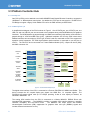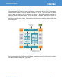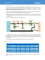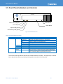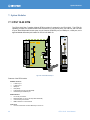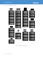
1
CPU 110-20 User Manual USER MANUAL CPU110-20 Core i7 3U VPX SBC Module First edition – August 2013 – CPU110-20MAN001 1 DIGITAL TECHNOLOGIES FOR A BETTER WORLD www.eurotech.com CPU110-20 User Manual CPU 110-20 User Manual This page intentionally left blank CPU 110-20 User Manual 2 Preface Preface Thank you for choosing the CPU110-20. Please read this manual before using the CPU110-20 so that you may obtain the greatest benefit from using the device. This manual presents the specifications, functions, and method of use of the CPU110-20. Eurotech has made every effort to carefully inspect each product and has taken great care to package and to ship the product. In the unlikely event of the product’s failure to operate normally due to problems in shipping or otherwise, the company will repair or replace the product at its own responsibility. If you have any questions, contact your local Eurotech Sales Office. See page 78 for full contact details. Trademarks All trademarks both marked and not marked appearing in this document are the property of their respective owners. This document does not give permission to the implementation of patents or other rights held by Eurotech or third parties. Document Revision History 3 VERSION DATE Publication Number First edition August 2013 Issued CPU110-20MAN001 CPU110-20 User Manual CPU110-20 User Manual Table of Contents DOCUMENT REVISION HISTORY ..................................................................................................................................................... 3 1. IMPORTANT USER INFORMATION ........................................................................................................................ 9 1.1 SAFETY NOTICES AND WARNINGS ............................................................................................................................................ 9 1.2 LIFE SUPPORT POLICY .......................................................................................................................................................... 11 1.3 WARRANTY ....................................................................................................................................................................... 11 1.4 ROHS ............................................................................................................................................................................... 11 1.5 TECHNICAL ASSISTANCE........................................................................................................................................................ 11 1.6 CONVENTIONS.................................................................................................................................................................... 12 1.7 REFERENCE DOCUMENTATION ............................................................................................................................................... 12 1.7.1 Standards ......................................................................................................................................................... 12 1.7.2 Product Specifications, Component Data Sheets, and Design Guides.............................................................. 13 2. SUMMARY ................................................................................................................................................................... 14 2.1. FEATURES ......................................................................................................................................................................... 15 2.2. BLOCK DIAGRAM ............................................................................................................................................................... 18 3. HARDWARE SPECIFICATIONS ....................................................................................................................................... 19 3.1. PROCESSOR ...................................................................................................................................................................... 19 3.1.1. Processor Options .................................................................................................................................................. 19 3.1.2. I/O Address Map .................................................................................................................................................... 20 3.1.3. Memory Address Map............................................................................................................................................ 20 3.2. MEMORY ......................................................................................................................................................................... 20 3.2.1. Main Memory ........................................................................................................................................................ 20 3.2.2. Boot ROM............................................................................................................................................................... 20 3.3 PLATFORM CONTROLLER HUB ............................................................................................................................................... 21 3.3.1 PCI Express ............................................................................................................................................................. 21 3.3.2 PCH Backplane I/O ................................................................................................................................................. 21 3.3.3 PCH General Purpose I/O ....................................................................................................................................... 22 3.4. GENERAL BOARD ARCHITECTURE .......................................................................................................................................... 23 3.4.1 PMC/XMC Site .................................................................................................................................................. 23 3.4.2 PLX PEX8616 PCIe Switch ................................................................................................................................. 23 3.4.3 Intel 82580 Quad 1Gb Ethernet Controller ...................................................................................................... 25 3.4.4 IDT Tsi382 PCIe to PCI Bridge for PMC Support................................................................................................ 26 3.4.5 SCH3112 Super I/O ........................................................................................................................................... 27 3.4.6 SM2242 Flash Controller and NAND Flash Memory ........................................................................................ 29 3.4.7 Trusted Platform Module (TPM).......................................................................................................................... 30 3.4.8 Clocks ............................................................................................................................................................... 31 3.4.9 SMBus Architecture .......................................................................................................................................... 32 3.4.10 JTAG Boundary Scan............................................................................................................................................ 33 3.4.11 Power Generation, Control, Monitoring, and Resets .......................................................................................... 34 3.5 FRONT PANEL INDICATORS AND CONTROLS ............................................................................................................................. 38 4. MECHANICAL SPECIFICATIONS ..................................................................................................................................... 39 4.1. EXTERNAL DIMENSIONS ...................................................................................................................................................... 39 4.2. INSTALLATION OF PMC/XMC MODULE................................................................................................................................. 40 4.3. HEAT SINK ........................................................................................................................................................................ 41 5. CONNECTORS AND JUMPERS ....................................................................................................................................... 42 5.1. CPU110-20 ON-BOARD COMPONENTS ................................................................................................................................ 42 CPU 110-20 User Manual 4 Table of Contents 5.2. SETUP.............................................................................................................................................................................. 43 5.2.1. JP2 (Reset RTC pin) ................................................................................................................................................. 43 5.2.1. JP3 (CMOS clear pin) .............................................................................................................................................. 43 5.3. PIN LAYOUT ...................................................................................................................................................................... 44 5.3.1. VPX P0 – Utility Connector ................................................................................................................................... 44 5.3.2 VPX P1 .................................................................................................................................................................... 44 5.3.3 VPX P2 .................................................................................................................................................................... 44 5.3.4 XMC J15.................................................................................................................................................................. 45 5.3.5 XMC J16.................................................................................................................................................................. 45 5.3.6 PMC J11 & J12 ........................................................................................................................................................ 46 5.3.7 J2 – Front Panel USB2.0 ......................................................................................................................................... 46 6. SYSTEM SPECIFICATIONS ............................................................................................................................................. 47 6.1. CHASSIS POWER SUPPLY REQUIREMENTS ............................................................................................................................... 47 6.2. ELECTRICAL SPECIFICATIONS ................................................................................................................................................. 47 6.2.1. GPIO ....................................................................................................................................................................... 47 6.3. ENVIRONMENTAL SPECIFICATIONS ......................................................................................................................................... 48 7. OPTION MODULES ...................................................................................................................................................... 49 7.1 CPU110-20 RTM ............................................................................................................................................................. 49 7.1.1 CPU110-20 RTM VPX I/O ........................................................................................................................................ 50 7.1.2 CPU110-20 RTM XMC I/O ...................................................................................................................................... 51 7.1.3 CPU110-20 RTM Rear Panel I/O ............................................................................................................................. 52 7.2 DYNATEM EXPANSION MODULE............................................................................................................................................ 53 8. BIOS SETUP .................................................................................................................................................................. 55 8.1. MAIN MENU .................................................................................................................................................................... 55 8.1.1. System Date ........................................................................................................................................................... 55 8.1.2. System Time ........................................................................................................................................................... 55 8.1.3. System Information ................................................................................................................................................ 55 8.1.4. Boot Features ......................................................................................................................................................... 56 8.1.5. Error Manager ....................................................................................................................................................... 56 8.2. ADVANCED MENU ............................................................................................................................................................ 57 8.2.1. Select Language ..................................................................................................................................................... 57 8.2.2. ACPI Configuration ................................................................................................................................................. 57 8.2.3. Processor Configuration ......................................................................................................................................... 58 8.2.4. Peripheral Configuration ........................................................................................................................................ 61 8.2.5. HDD Configuration ................................................................................................................................................. 61 8.2.6. Memory Configuration........................................................................................................................................... 62 8.2.7. System Agent (SA) Configuration ........................................................................................................................... 63 8.2.8. South Bridge Configuration.................................................................................................................................... 67 8.2.9. Network Configuration .......................................................................................................................................... 70 8.2.10. LPC Configuration ................................................................................................................................................ 71 8.2.11. SMBIOS Event Log ................................................................................................................................................ 71 8.2.12. ME Configuration ................................................................................................................................................. 72 8.2.13. Thermal Configuration ......................................................................................................................................... 73 8.2.14. ICC Configuration ................................................................................................................................................. 75 8.2.15. Intel Rapid Start Technology ................................................................................................................................ 75 8.3. SECURITY MENU .............................................................................................................................................................. 76 8.4. BOOT MENU .................................................................................................................................................................... 76 8.5. EXIT MENU ..................................................................................................................................................................... 76 EUROTECH WORLDWIDE PRESENCE ................................................................................................................................ 77 5 CPU110-20 User Manual CPU110-20 User Manual List of Figures FIGURE 1: CPU 110-20 BLOCK DIAGRAM ....................................................................................................................................... 18 FIGURE 2: CPU BLOCK DIAGRAM ................................................................................................................................................... 19 FIGURE 3: CPU 110-20 PCH BACKPLANE I/O ................................................................................................................................. 21 FIGURE 4: PEX8616 PCIE SWITCH BLOCK DIAGRAM ......................................................................................................................... 23 FIGURE 5: PEX8616 OPENVPX DATA PLANE CONFIGURATIONS .......................................................................................................... 24 FIGURE 6: PEX8616 EXAMPLE NON-TRANSPARENT CONFIGURATION ................................................................................................... 24 FIGURE 7: INTEL 82580 QUAD GBE CONTROLLER BLOCK DIAGRAM...................................................................................................... 25 FIGURE 8: TSI382 PCIE TO PCI BRIDGE BLOCK DIAGRAM ................................................................................................................... 26 FIGURE 9: SUPER I/O BLOCK DIAGRAM ........................................................................................................................................... 27 FIGURE 10: SM2242 FLASH CONTROLLER BLOCK DIAGRAM ............................................................................................................... 29 FIGURE 11: TRUSTED PLATFORM MODULE BLOCK DIAGRAM ............................................................................................................... 30 FIGURE 12: CLOCK DISTRIBUTION ................................................................................................................................................... 31 FIGURE 13: SMBUS ARCHITECTURE ................................................................................................................................................ 32 FIGURE 14: JTAG BOUNDARY SCAN BLOCK DIAGRAM ........................................................................................................................ 33 FIGURE 15: CPU110-20 POWER SUPPLY STRUCTURE ........................................................................................................................ 35 FIGURE 16: CONTROL, MONITORING, AND RESET STRUCTURE.............................................................................................................. 37 FIGURE 17: CPU110-20 FRONT PANEL .......................................................................................................................................... 38 FIGURE 18: EXTERNAL DIMENSIONS OF CPU110-20.......................................................................................................................... 39 FIGURE 19: PMC/XMC INSTALLATION............................................................................................................................................ 40 FIGURE 20: CPU110-20 HEAT SINK ............................................................................................................................................... 41 FIGURE 21: TOP SIDE OUTLINE........................................................................................................................................................ 42 FIGURE 22: BOTTOM SIDE OUTLINE ................................................................................................................................................ 42 FIGURE 23: FRONT PANEL USB PIN ASSIGNMENTS ............................................................................................................................ 46 FIGURE 24: CPU110-20 RTM LAYOUT .......................................................................................................................................... 49 FIGURE 25: CPU110-20 RTM VPX PIN ASSIGNMENTS ..................................................................................................................... 50 FIGURE 26: SAMTEC QSH SERIES HIGH-SPEED DIFFERENTIAL CONNECTOR ............................................................................................. 51 FIGURE 27: RTM REAR PANEL I/O PIN ASSIGNMENTS ....................................................................................................................... 52 FIGURE 28: CPU110-20/DXM STACKUP........................................................................................................................................ 53 FIGURE 29: EXAMPLE DXM EQUIPPED FRONT PANEL......................................................................................................................... 53 FIGURE 30: CPU110-20/DXM/PMC/XMC CROSS SECTION ............................................................................................................ 54 CPU 110-20 User Manual 6 Table of Contents List of Tables TABLE 1: PROCESSOR OPTIONS....................................................................................................................................................... 19 TABLE 2: I/O SPACE ADDRESS MAP................................................................................................................................................. 20 TABLE 3: MEMORY SPACE ADDRESS MAP ......................................................................................................................................... 20 TABLE 4: CPU 110-20 PCH GPIO ASSIGNMENTS ............................................................................................................................ 22 TABLE 5: HDMI LEVEL TRANSLATOR GPIO EQUALIZATION CONTROL .................................................................................................... 22 TABLE 6: HDMI LEVEL TRANSLATOR GPIO OUTPUT CONTROL ............................................................................................................ 22 TABLE 7: SUPER I/O DEVICE MAP................................................................................................................................................... 27 TABLE 8: SUPER I/O GPIO ASSIGNMENTS ........................................................................................................................................ 28 TABLE 9: PRIMARY CPU110-20 CLOCKS ......................................................................................................................................... 31 TABLE 10: SMBUS SLAVE ADDRESSES ............................................................................................................................................. 32 TABLE 11: CPU110-20 SUPPLY RAIL SUMMARY ............................................................................................................................... 36 TABLE 12: CPU110-20 SUPPORTED POWER STATES ......................................................................................................................... 36 TABLE 13: FRONT PANEL INDICATORS AND CONTROLS ........................................................................................................................ 38 TABLE 14: MECHANICAL SPECIFICATIONS ......................................................................................................................................... 39 TABLE 15: RESET RTC JUMPER SETTINGS ......................................................................................................................................... 43 TABLE 16: CLEAR CMOS JUMPER SETTINGS ..................................................................................................................................... 43 TABLE 17: VPX P0 PIN ASSIGNMENTS............................................................................................................................................. 44 TABLE 18: VPX P1 PIN ASSIGNMENTS............................................................................................................................................. 44 TABLE 19: VPX P2 PIN ASSIGNMENTS............................................................................................................................................. 44 TABLE 20: XMC J15 PIN ASSIGNMENTS .......................................................................................................................................... 45 TABLE 21: XMC J16 PIN ASSIGNMENTS .......................................................................................................................................... 45 TABLE 22: PMC J11, J12 PIN ASSIGNMENTS ................................................................................................................................... 46 TABLE 23: POWER SUPPLY SPECIFICATIONS ....................................................................................................................................... 47 TABLE 24: GPIO ELECTRICAL SPECIFICATIONS .................................................................................................................................... 47 TABLE 25: ENVIRONMENTAL SPECIFICATIONS .................................................................................................................................... 48 TABLE 26: RTM XMC I/O PIN ASSIGNMENTS .................................................................................................................................. 51 TABLE 27: SYSTEM DATE MENU SETTINGS ....................................................................................................................................... 55 TABLE 28: SYSTEM TIME MENU SETTINGS ........................................................................................................................................ 55 TABLE 29: BOOT FEATURES MENU SETTINGS .................................................................................................................................... 56 TABLE 30: ERROR MANAGER ......................................................................................................................................................... 56 TABLE 31: SELECT LANGUAGE SETTINGS ........................................................................................................................................... 57 TABLE 32: ACPI CONFIGURATION SETTINGS ..................................................................................................................................... 57 TABLE 33: PROCESSOR CONFIGURATION SETTINGS ............................................................................................................................. 58 TABLE 34: PROCESSOR POWER MANAGEMENT SETTINGS .................................................................................................................... 59 TABLE 35: PERIPHERAL CONFIGURATION SETTINGS ............................................................................................................................ 61 TABLE 36: HDD CONFIGURATION SETTINGS ..................................................................................................................................... 61 TABLE 37: MEMORY CONFIGURATION SETTINGS................................................................................................................................ 62 TABLE 38: DMI SETTINGS ............................................................................................................................................................. 63 TABLE 39: INTEL (R) VT FOR DIRECTED I/O(VT-D)SETTINGS ............................................................................................................... 63 TABLE 40: GRAPHICS CONFIGURATION SETTINGS ............................................................................................................................... 63 TABLE 41: PEG PORT CONFIGURATION SETTINGS .............................................................................................................................. 66 TABLE 42: SOUTH BRIDGE CONFIGURATION SETTINGS ........................................................................................................................ 67 TABLE 43: SB PCI EXPRESS CONFIGURATION SETTINGS....................................................................................................................... 67 TABLE 44: PCI EXPRESS PORT 1 CONFIGURATION (PCIE/PCI-BRIDGE) SETTINGS..................................................................................... 68 TABLE 45: PCI EXPRESS PORT 3~5 CONFIGURATION SETTINGS .......................................................................................................... 69 TABLE 46: SB USB CONFIGURATION SETTINGS ................................................................................................................................. 69 TABLE 47: SB SERIAL IRQ CONFIGURATION SETTINGS ........................................................................................................................ 70 TABLE 48: NETWORK CONFIGURATION SETTINGS............................................................................................................................... 70 TABLE 49: LPC CONFIGURATION SETTINGS ....................................................................................................................................... 71 TABLE 50: SMBIOS EVENT LOG SETTINGS ....................................................................................................................................... 71 TABLE 51: ME CONFIGURATION SETTINGS ....................................................................................................................................... 72 7 CPU110-20 User Manual CPU110-20 User Manual TABLE 52: TABLE 53: TABLE 54: TABLE 55: TABLE 56: TABLE 57: THERMAL CONFIGURATION SETTINGS ............................................................................................................................... 73 DIV-2S SETTINGS ......................................................................................................................................................... 75 INTEL RAPID START TECHNOLOGY SETTINGS ....................................................................................................................... 75 SECURITY MENU SETTINGS ............................................................................................................................................. 76 BOOT MENU SETTINGS .................................................................................................................................................. 76 EXIT MENU SETTINGS .................................................................................................................................................... 76 CPU 110-20 User Manual 8 User Information 1. Important User Information In order to lower the risk of personal injury, electric shock, fire, or equipment damage, users must observe the following precautions as well as good technical judgment, whenever this product is installed or used. All reasonable efforts have been made to ensure the accuracy of this document; however, Eurotech assumes no liability resulting from any error/omission in this document or from the use of the information contained herein. Eurotech reserves the right to revise this document and to change its contents at any time without obligation to notify any person of such revision or changes. Reproduction of all or part of this document without Eurotech’s permission is prohibited. 1.1 Safety Notices and Warnings The following general safety precautions must be observed during all phases of operation, service, and repair of this equipment. Failure to comply with these precautions or with specific warnings elsewhere in this manual violates safety standards of design, manufacture, and intended use of the equipment. Eurotech assumes no liability for the customer’s failure to comply with these requirements. The safety precautions listed below represent warnings of certain dangers of which Eurotech is aware. You, as the user of the product, should follow these warnings and all other safety precautions necessary for the safe operation of the equipment in your operating environment. Alerts that can be found throughout this manual The following alerts are used within this manual and indicate potentially dangerous situations. Danger, electrical shock hazard: Information regarding potential electrical shock hazards: Personal injury or death could occur. Also damage to the system, connected peripheral devices, or software could occur if the warnings are not carefully followed. Appropriate safety precautions should always be used, these should meet the requirements set out for the environment that the equipment will be deployed in. Warning: Information regarding potential hazards: Personal injury or death could occur. Also damage to the system, connected peripheral devices, or software could occur if the warnings are not carefully followed. Appropriate safety precautions should always be used, these should meet the requirements set out for the environment that the equipment will be deployed in. Electrostatic Discharge Warning: Appropriate ESD safeguards should be taken to prevent damage to the product. 9 CPU110-20 User Manual CPU110-20 User Manual Information and/or Notes: These will highlight important features or instructions that should be observed. Protect the device from vibration and impact Do not place the product in a location where it can fall or can be subject to vibration or impact because this may cause device failure. Do not modify the device For safety reasons, under no circumstances should you modify the device. products that have been modified. Eurotech will not repair Protect the product from water and chemicals Contact between the product and water or chemicals can result in product failure, electrocution, or fire. Protect the product from foreign material Make sure that foreign material does not get into the product during use, storage, or transport because this can result in product failure. Use precautions in handling to ensure that you are not injured The sharp projections on this product may cause injury. Take care in handling this product in order to avoid injury. Do not disassemble the product In order to maintain guaranteed product performance, do not disassemble this product under any circumstances. Keep the product away from radios and TVs Do not use the product near radios, television sets, or other devices generating strong magnetic or electrical fields. This could result in failure or malfunction. Keep the product away from flame, humidity, and direct sunlight Do not use or store the product in any of the following locations, as this could result in product failure: Places where there is fire Locations high in humidity or exposed to rain Locations exposed to direct sunlight Dusty or dirty locations Locations containing excessive water or chemical vapours Install the product in well-ventilated locations Install the product in well-ventilated locations to efficiently disperse heat generated by the product. Remove the power plug from the receptacle when not using the product Turn off the main switch and remove the power plug from the receptacle when not using the product or when there is the risk of lightning strike. Use the device within rated parameters Be sure to use the product within the ratings specified in this manual. Failure to do so may result in malfunction. CPU 110-20 User Manual 10 User Information Use care when cleaning the product If the product becomes dirty, wipe it with a dry soft cloth. A thinned neutral cleaner may be used if the product is particularly dirty. Do not use benzene, thinners, or other solvents under any circumstances. Ground the product in order to prevent electrocution Be sure to ground the product by connecting it to a 3-pole AC receptacle or by using an AC receptacle having a grounding terminal. Dispose of the product properly Use appropriate methods for handling industrial wastes when disposing of this product. Wire the product correctly Failure to wire the product correctly can result in malfunction or fire. Read this manual and wire the product correctly. Use antistatic precautions This product comprises electronic parts that are highly susceptible to static electricity. Static electricity can cause the product to malfunction. Take care not to touch any of the terminals, connectors, ICs, or other parts with the hands. Do not use a malfunctioning product Stop using the product if you believe it is malfunctioning. Continuing to use a malfunctioning product can cause the malfunction to spread to other products and can cause short circuits or fire. 1.2 Life Support Policy Eurotech products are not authorized for use as critical components in life support devices or systems without the express written approval of Eurotech. 1.3 Warranty For warranty terms and conditions users should contact their local Eurotech Sales Office. See , page 75 for full contact details. 1.4 RoHS This device, including all its components, subassemblies and the consumable materials that are an integral part of the product, has been manufactured in compliance with the European directive 2002/95/EC known as the RoHS directive (Restrictions on the use of certain Hazardous Substances). This directive targets the reduction of certain hazardous substances previously used in electrical and electronic equipment (EEE). 1.5 Technical Assistance If you have any technical questions, cannot isolate a problem with your device, or have any enquiry about repair and returns policies, contact your local Eurotech Technical Support Team. See Eurotech Worldwide Presence, page 55 for full contact details. 11 CPU110-20 User Manual CPU110-20 User Manual Transportation When transporting any module or system, for any reason, it should be packed using anti-static material and placed in a sturdy box with enough packing material to adequately cushion it. Warning: Any product returned to Eurotech that is damaged due to inappropriate packaging will not be covered by the warranty. 1.6 Conventions The following table describes the conventions for signal names used in this document. Convention GND # + NC RSVD Explanation Digital ground plane Active low signal Positive signal in differential pair Negative signal in differential pair No connection Use is reserved to Eurotech 1.7 Reference Documentation Listed below are documents that describe applicable standards, the processor and chipset, and the peripheral components used on the CPU110-20. It is beyond the scope of this document to detail operation of each component. It is imperative that the user either download applicable data sheets from the Internet or contact your local distributor for copies of these documents. Many of the documents are confidential and may require execution of a non-disclosure agreement between the supplier and CPU11020 user. 1.7.1 • • • • • • • • • • Standards VITA 20-2001 - Conduction Cooled PMC, R1.1, February 2005 VITA 32-2003 - Processor PMC, R1.0, July 2003 VITA 42.0-2005 - XMC Switched Mezzanine Card Baseline Standard, D0.29, September 2005 VITA 42.3-2006 - XMC PCI Express Protocol Layer Standard, R1.0, June 2006 VITA 42.6-200x - XMC 10 Gigabit Ethernet 4-Lane Protocol Layer Standard, R0.911, January 2009 VITA 46.0-2007 - VPX Baseline Standard, R1.2, April 2008 VITA 46.4-2008 - PCI Express on VPX Fabric Connector, R6.00, March 2008 VITA 46.9-2005 - PMC/XMC Pinout Mapping, R0.1, May 2005 IEEE P1386 - Common Mezzanine Card Family (CMC), D2.4a, March 2001 IEEE P1386.1 - CMC Physical and Environmental Layers, D2.4, January 2001 CPU 110-20 User Manual 12 User Information 1.7.2 • • • Product Specifications, Component Data Sheets, and Design Guides CPU 110-20 Data Sheet, R0.1, May 2013 CPU 110-20 Schematic Diagram, R0.1, May 2013 CPU 110-20 Bill of Materials, R0.1, May 2013 Many of Intel's documents are confidential and cannot be distributed to third parties. Most of the documents listed below can be downloaded from the Intel Business Link (IBL) website. Contact your Intel sales representative and request IBL access to Intel Chief River Platform documentation. • • • • • • • • • • • • • • • • 13 ® Intel Mobile 3rd Generation Core Processor Family External Design Specification, Vol. 1, Rev. 2.0, February 2012 ® Intel Chief River Platform Design Guide, Doc. No. 471984, Rev. 2.0, February 2012 ® Intel Embedded Chief River +ECC Platform Design Guide Addendum, Doc. No. 472868, Rev. 1.7, December 2011 ® Intel 7 Series/C216 Chipset Family Platform Controller Hub (PCH), Doc. No. 474146, Rev. 1.8, November 2011 PLX PEX8616 16-Lane 4-Port PCI Express Gen2 Switch Data Book, Version 1.3, June 2012 IDT Tsi382 PCIe to PCI Bridge User Manual, 80E2010_AM001_06, August 2009 ® Intel 82580 Quad/Dual Gigabit Ethernet LAN Controller Datasheet, Doc. No. 321027-011EN, Rev. 2.3, March 2010 Micron MT41J512M8 DDR3 SDRAM Datasheet, Doc. No. 09005aef8417277b, Rev. I, February 2012 Micron MT29F128G08 NAND Flash Memory Datasheet, Doc. No. 09005aef836c9ded, Rev. F, December 2009 SMSC SCH3112 LPC IO (Super IO) Datasheet, Rev. 1.0, November 2006 Silicon Motion SM2242 Serial ATA to Flash Memory Datasheet, Rev.0.2, February 2009 Atmel AT97SC3204 TPM with LPC Bus Data sheet, Rev.5294BS−TPM−10/10, October 2010 Linear Technology LTM4616 Dual 8A Low-Vin DC/DC Module Datasheet, Doc. No. LT 1108, Rev. A, 2008 Linear Technology LTM3026 1.5A Low Input Voltage VLDO Linear Regulator, Doc. No. LT 0707 REV B, 2005 Texas Instruments TPS59650 Dual-Channel (3-Phase CPU/2-Phase GPU) SVID, D-CAP+™ Step-Down Controller for IMVP-7 VCORE with Two Integrated Drivers Data Sheet, Document No. SLUSAV7, January 2012 Lattice Semiconductor ispPAC-POWR1220AT8 Power Supply Monitor/Sequencer/Controller Datasheet, Doc. No. DS1015, June 2008 CPU110-20 User Manual CPU110-20 User Manual 2. Summary The CPU 110-20 is a high performance Single Board Computer (SBC) based on the 3U OpenVPX™ (VITA 65) form factor. Offered in both convection cooled and ruggedized conduction cooled variants, the CPU 110-20 will meet the needs of numerous commercial and military applications requiring maximum processing power, low power consumption, and small physical footprint. The CPU 110-20 adheres to the OpenVPX™ standard for a 3U Payload Module Profiles designated as MOD3-PAY-2F2T-16.2.5-4, MOD3-PAY-2F2U-16.2.3-3, or MOD3-PAY-1D-16.2.6-2. The first two profiles consist of a dual x4 Gen2 PCI Express Data Plane and either dual 1000BASE-T Gigabit Ethernet or dual 1000BASE-BX control planes. The third profile consists of a double fat pipe or x8 Gen2 PCIe data plane. XMC Site I/O to the VPX backplane consists 12 dedicated differential pairs which follow the VITA 46.9 P2w11-X12d XMC I/O standard. At the heart of the CPU 110-20 is an Intel® 2nd Generation Core™ i7 Ivy Bridge Quad Core Processor and Panther Point QM77 Platform Controller Hub (PCH). These two devices form the central processing backbone of the design. With a dual-channel memory controller integrated in the processor, the CPU 11020 supports up to 8 GBytes of DDR3 SDRAM running at up to 1667 MHz. One of the processor's x8 Gen2 PCI Express (PCIe) ports is connected to a PLX PEX8616 PCIe switch. The downstream ports of the switch then connect to the VPX backplane data plane. The processor's second x8 Gen 2 PCIe port is connected to the XMC site per VITA42.3. The PEX8616 switch can support non-transparent operation on one of the downstream VPX ports, effectively making it a nontransparent upstream port to a second processor memory domain. The QM77 PCH utilizes the following interfaces in the CPU 110-20: PCI Express (PCIe); both 3G and 6G Serial ATA (SATA); both Universal Serial Bus 2.0 and 3.0; High Definition Audio; DVI/HDMI; VGA; LPC Bus; SMBus; and, General Purpose I/O. One PCH x4 PCIe port is attached to an Intel® 82580EB Quad Gigabit Ethernet Controller to support the 1000Base-T or -BX backplane control plane. An additional x1 PCIe port is connected to a Tsi382 PCIe to PCI Bridge to support a legacy 32-bit 66MHz PCI bus for the PMC interface per IEEE1386.1. One 6G SATA port, one 3G SATA port, one USB 3.0, and one USB 2.0 port are connected to the backplane along with DVI/HDMI and VGA graphics interfaces. Additional backplane I/O from the PCH include three SMBus interfaces, two connecting to VPX P0 per VITA 46.0 and one connected to VPX P2 to support rear transition module expansion. The PCH High Definition Audio Interface is connected to user I/O pins on VPX P1. The PCH LPC bus is connected to a Trusted Platform Module and a Super I/O device. Backplane I/O from the Super I/O consists of two RS232/485 ports and PS2 keyboard/Mouse interface or 4-bit GPIO. CPU 110-20 User Manual 14 Summary CPU 110-20 on-board storage consists of a SATA based SM2240 Flash Controller supporting 16GBytes of solid state storage and two 32Mbit SPI PROMs providing 8MBytes of in-circuit programmable boot code. Front panel I/O consists of a single USB 2.0 port. The CPU110-20 supports two Dynatem option modules: a rear transition module and a front panel I/O expansion module called the DXM. The CPU110-20 Rear Transition Module (RTM) provides I/O support for the CPU110-20. This RTM I/O capability provides rear chassis headers and connectors for: two SATA ports; one USB 3.0 and one USB 2.0 port; Dual-RS232/485 Console ports; a multi-function GPIO/PS2 port; an HDMI port, a VGA port; and a high-bandwidth differential pair header for CPU110-20 XMC I/O. The CPU 110-20 also supports the Dynatem eXpansion Module (DXM) which provides I/O expansion by increasing front panel width, stacking the PMC/XMC site, and utilizing additional front panel space for I/O connectors. DXM I/O from the CPU 110-20 consists of one SATA 2.0 port, two USB 2.0 ports, and two 1000BASE-BX ports with sideband signals. The DXM also provides support for programming and debug of CPU 110-20 hardware and software. 2.1. Features CPU • • • • • • • • • • • • • • • • • • rd 3 Generation Intel® Core i7 Processor support for: o i7-3615QE 45W Quad-Core o i7-3612QE 35W Dual-core Ivy Bridge Processor running at up to 3.10 GHz o i7-3555LE 25W Dual-Core Ivy Bridge Processor running at up to 3.20 GHz o i7-3517UE 17W Dual-Core Ivy Bridge Processor running at up to 2.80 GHz Direct Media Interface Bus supporting 5GByte/Sec transfer rates Dual Memory Controller supporting up to 8GBytes DDR3 SDRAM at up to 800 MHz (1600 MHz DDR) x8 Gen2 PCIe Port 0 connected to XMC Connector J15 x8 Gen2 PCIe Port 1 connected to a PLX PEX8616 PCIe Switch Integrated Graphics Controller A 32-KB instruction and 32-KB data first-level cache (L1) for each core A 256-KB shared instruction/data second-level cache (L2) for each core Up to 8-MB shared instruction/data third-level cache (L3), shared among all cores Intel® Virtualization Technology (Intel® VT-x) Intel® Virtualization Technology for Directed I/O (Intel® VT-d) Intel® Trusted Execution Technology (Intel® TXT) Intel® Streaming SIMD Extensions 4.1 (Intel® SSE4.1) Intel® Streaming SIMD Extensions 4.2 (Intel® SSE4.2) Intel® Hyper-Threading Technology (Intel® HT Technology) Intel® 64 architecture Intel® Turbo Boost Technology Intel® Advanced Vector Extensions (Intel AVX) Platform Controller Hub (PCH) • • • • • • • • • 15 Intel® Panther Point QM77 Platform Controller Hub PCI Express Base Specification, Revision 2.0 support for up to eight ports at 5GT/s transfer speeds ACPI Power Management Logic Support, Revision 3.0b Enhanced DMA controller, interrupt controller, and timer functions Integrated 6G and 3G Serial ATA host controllers with independent DMA operation on up to six ports USB host interface consisting of two EHCI high-speed USB 2.0 Host controllers with 2 rate matching hubs and one xHCI USB 3.0 controller System Management Bus (SMBus) Specification, Version 2.0 with additional support for on-board I2C devices Supports Intel® High Definition Audio Supports Intel® Rapid Storage and Active Management Technology CPU110-20 User Manual CPU110-20 User Manual • • • • • Supports Intel® Virtualization Technology for Directed I/O Supports Intel® Trusted Execution Technology Digital Display port (HDMI/DVI) and Analog Display port (VGA) Low Pin Count (LPC) interface Serial Peripheral Interface (SPI) PLX Technology PEX8616 16-Lane 4-Port Gen2 PCIe Switch • • • Low-Latency non-blocking switch fabric VPX ports can be configured as (1) x8 or (2) x4 One downstream VPX port can operate in non-transparent mode to support multi-master environments Intel® 82580DB Quad 1 Gigabit Ethernet Controller (Control Plane) • • • • • Complies with 1Gb/Sec Ethernet/802.3ap x4 PCI Express interface to PCH IEEE1588 Precision Time Protocol (PTP) support 4-Wire SPI EEPROM Interface Supports both SERDES and MDI interfaces SMSC SCH3112 Super I/O • • • LPC Interface to PCH Dual Serial Ports with asynchronous baud rates up to 1.5Mbps RS485 Auto Direction Control Mode Silicon Motion SM2242 Serial ATA to NAND Flash Controller • • • • Compliant with SATA Rev. 2.6 Specification Dual channel 8-bit flash interface Up to 50MB/Sec for Read, 40MByte/Sec Write ECC and wear leveling support Atmel AT97SC3204 Trusted Platform Module • • • • Full Trusted Computing Group (TCG) Trusted Platform Module (TPM) Version 1.2 compatibility Hardware Asymmetric Crypto Engine 2048-bit RSA® Sign in 500 ms Internal EEPROM Storage for RSA Keys IDT Tsi382 PCIe to PCI Bridge • • x1 PCIe from PCH to 32-bit 66MHz PCI bus Non-Transparent operation supported PMC/XMC/DXM Site • • • • 32-Bit 66MHz PCI Bus from Tsi382 to PMC via J11 and J12 x8 Gen2 PCI Express Bus from CPU to XMC via J15 12 differential pairs from XMC J16 to VPX P1, capable of 3.125Gbit/Sec rate per differential pair Dynatem eXpansion Module provides I/O expansion by increasing front panel width, stacking the PMC/XMC site, and utilizing additional panel space for I/O connectors (see DXM data sheet) VPX Rear I/O • • • P0 Utility Connectivity per VITA 46.0 including dual SMBus P1 Fabric Connectivity per VITA 65, MOD3-PAY-2F2T-16.2.5-4 or MOD3-PAY-2F2U-16.2.3.3 and High Definition Audio Interface P2 Module I/O: SATA, USB, HDMI, VGA, SMBus, GPIO, and Dual RS232 or RS485, and P2w11-X12d XMC I/O per VITA 46.9 Non-Volatile Storage • • 64Mbit EEPROM on PCH SPI bus 16GByte Solid State SATA Flash Drive CPU 110-20 User Manual 16 Summary Miscellaneous • • • On-board temperature monitoring via SMBus Front Panel USB 2.0 Port (Type A) Jumper selectable XMC VPWR (5V or +12V) Power Consumption (subject to change without notice) • • • • • • +3.3V @ tbd A (typ) +5V @ tbd A (typ) +12V @ tbd A (typ) +3.3VAUX @ tbd A (typ) Total Power: tbd W (typ) Actual power depends on CPU 110-20 product configuration as well as PMC/XMC/DXM and Front Panel USB loads Form Factor • 3U VITA 65 OpenVPX Rugged/Conduction Cooled • Available as a conduction cooled • Wedge locks provide high shock and vibration immunity per MIL-STD-810F • Optional conformal coating is available 17 CPU110-20 User Manual CPU110-20 User Manual 2.2. Block Diagram The CPU 110-20 Block Diagram is shown in Figure 1. DDR3 - 1677 12.8GB/Sec Intel Core i7-2655LE Ivy Bridge CPU DDR3 - 1677 12.8GB/Sec PCIe x8 Gen2 8GB/Sec 4GByte DDR3 ECC SDRAM 4GByte DDR3 ECC SDRAM Data Plane 1 (1) Fat Pipe Data Plane 2 (1) Fat Pipe PCIe x4 Gen2 PEX8616 PCIe Switch 4GB/Sec PCIe x4 Gen2 4GB/Sec XMC J15 PCIe x8 Gen2 8GB/Sec FDI VITA 42.3 DMI 2.5GB/Sec VPX P1 PCIe x1 Gen1 512MB/Sec IDT Tsi382 PCIe to PCI Bridge PMC J11-J12 32-Bit/66MHz PCI 266MB/Sec IEEE P1386 Board I/O HIGH DEFINITION AUDIO MAG 1000BASE-T or BX MAG 1000BASE-T or BX Control Plane 1 (1) TP or (1) UTP Control Plane 2 (1) TP or (1) UTP 125MB/Sec PCIe x4 Gen2 4GB/Sec Intel 82580 Quad GigE Controller 125MB/Sec 125MB/Sec Up to 3GB/Sec 1000BASE-BX 1.25Gbps 12 Diff Pairs 1000BASE-BX 3.125Gbit/Sec/pair XMC J16 125MB/Sec SATA VITA 46.9 XMC I/O P2w11-X12d MISC DBG/PGM 300MB/Sec Intel Panther Point QM77 PCH (2) USB 60MB/Sec ea. PMC/XMC/DXM Site TPM LPC BUS 16.67MB/Sec SMSC SCH3112 Super I/O (2) COM Ports PS2 Keyboard/Mouse (4) GPIO RS232 RS485 XCVR VPX P2 Passive MUX Board I/O (1) USB 3.0 and (1) USB 2.0 625MB/Sec and 60MB/Sec (1) SATA 6G and (1) SATA 3G 600MB/Sec and 300MB/Sec HDMI/VGA SM Bus FRONT PNL USB USB 2.0 SPI BUS 64Mbit 32Mbit SPI PROM SPI SATA SM2242 SATA to Flash Controller 300MB/Sec FLASH BUS 40MB/Sec 16GByte NAND Flash Figure 1: CPU 110-20 Block Diagram CPU 110-20 User Manual 18 Hardware Specifications 3. Hardware Specifications 3.1. Processor 3.1.1. Processor Options The CPU 110-20 can support a wide variety of Intel Core processors, from high-performance quad-core to ultra-low power dual-core devices. A list of supported processors is shown in Table 1 below. These are targeted for mobile applications and are housed in ball-grid-array (BGA) packages. These are soldered directly to the PCB and are not field replaceable. Table 1: Processor Options Processor Description TDP (W) i7-3615QE Quad-core, 6M cache 45 i7-3612QE Quad-core, 6M cache (note 1) 35 i7-3555LE Dual-core, 4M cache (note 1) 25 i7-3517UE Dual-core, 4M cache 17 Note 1: Available only as a special order option. Please contact Dynatem for details. Speed (GHz) 3.30 3.10 3.20 2.80 CPU 110-20 CPU (U53) I/O consists of dual x8 Gen2 PCIe interfaces, dual DDR3 Memory Interfaces, and a PCH interface consisting of a Direct Memory Interface (DMI) and a Flexible Display Interface (FDI). The PCIe ports are connected to the PEX8616 PCIe Switch (U75) and XMC J15 Connector. Each memory controller is connected to (9) 512Mbit DDR3 SDRAM's in a "memory-down" configuration. 4GByte DDR3 SDRAM + ECC DDR3-1600 4GByte DDR3 SDRAM + ECC DDR3-1600 DDR3 Memory Controller CH. A DDR3 Memory Controller CH. B Gen 2 PCIe Port 0 x8 Gen2 PCIe Gen 2 PCIe Port 1 x8 Gen2 PCIe PEX8616 PCIe Switch CPU PCH Interface XMC J15 DMI and FDI Busses Figure 2: CPU Block Diagram 19 CPU110-20 User Manual CPU110-20 User Manual 3.1.2. I/O Address Map Hung… Check this Table. Table 2: I/O space Address Map DMA Controller 0000h - 001Fh DMA Controller 0093h - 009Fh Interrupt Controller 0020h - 002Dh Interrupt Controller 00A0h - 00B1h LPC SIO 002Eh - 002Fh Power Management 00B2h - 00B3h Interrupt Controller 0030h - 003Dh Interrupt Controller 00B4h - 00BDh Timer/Counter 0040h - 0043h DMA Controller 00C0h - 00DFh LPC SIO 004Eh - 004Fh PCI and Master Abort Timer/Counter 0050h - 0053h Serial ATA 0170h - 0177h Microcontroller 0060h Serial ATA 01F0h - 01F7h NMI Controller 0061h Serial ATA 0376h Microcontroller 0062h - 0066h Serial ATA RTC Controller 0070h - 0077h Interrupt Controller DMA Controller 0080h - 0091h Reset Generator Reset Generator 0092h 00F0h 03F6h 04D0h - 04D1h 0CF9h 3.1.3. Memory Address Map Hung… Check this Table. Table 3: Memory space Address Map Main Memory 0000_0000h --- 000D_FFFFh LPC(BIOS)(*1) 000E_0000h --- 000F_FFFFh Main Memory / PCI Device 0010_0000h --- TOM(*2) I/O APIC FEC0_0000h --- FECF_FFFFh High Precision Event Timers FED0_0000h --- FED0_33FFh TPM on LPC FED4_0000h --- FED4_BFFFh LPC(BIOS)(*1) FF00_0000h --- FFFF_FFFFh *1: Occupied area depends on the setting of Firmware Hub Decode Enable. *2: Most significant address depends on the setting of TOM register. For detailed technical information on the processor, please refer to the Intel® Mobile 3rd Generation Core Processor Family External Design Specification, Vol. 1, Rev. 2.0, February 2012. 3.2. Memory 3.2.1. Main Memory The processor includes an integrated dual-channel memory controller capable of supporting up to 4 GB of ECC DDR3 SDRAM memory per channel, running at speeds up to DDR3-1600. ECC automatically corrects 1-bit errors and detects 2-bit errors. Eighteen 4 Gbit Micron MT41J512M8RH-125 devices (nine per channel) are arranged in a “memory down” configuration. 3.2.2. Boot ROM This is dual SPI-FLASH memory devices (SST25VF032B) directly-mounted on CPU 110-20 with 8MB of capacity. BIOS and configuration data are stored in the SPI Flash devices. CPU 110-20 User Manual 20 Hardware Specifications 3.3 Platform Controller Hub 3.3.1 PCI Express One PCH x4 PCIe port is attached to an Intel® 82580EB Quad Gigabit Ethernet Controller to support the 1000Base-T or -BX backplane control plane. An additional x1 PCIe port is connected to a Tsi382 PCIe to PCI Bridge to support a legacy 32-bit 66MHz PCI bus for the PMC interface per IEEE1386.1. 3.3.2 PCH Backplane I/O A simplified block diagram of the PCH is shown in Figure 3. One 6G SATA port, one 3G SATA port, one USB 3.0, and one USB 2.0 port are connected to the backplane along with DVI/HDMI and VGA graphics interfaces. The HDMI interface is passed through an HDMI level translator (U39) and the VGA interface is passed through a VGA Driver/EMI Filter (U35). Additional backplane I/O from the PCH include three SMBus interfaces, two connecting to VPX P0 per VITA 46.0 and one connected to VPX P2 to support rear transition module expansion. The PCH High Definition Audio Interface is connected to user I/O pins on VPX P1. The PCH LPC bus is connected to a Trusted Platform Module (U67), a Super I/O device (U20), and XMC connector J16. TO/FROM CPU DMI INTERFACE TO/FROM CPU FDI INTERFACE TO/FROM TSI382 TO/FROM 82580 6G SATA SATA Controller USB 3.0 USB Controller (x1) PCIe INTERFACE (4) PCIe INTERFACE TO/FROM VPX P0 TO/FROM BOARD DEVICES SMBUS INTERFACE TO BOARD DEVICES CLOCK GENERATOR 3G SATA QM77 PCH USB 2.0 USB 2.0 Front Panel USB Digital Video Interface HDMI Level Translator Analog Video Interface VGA Driver & EMI Filter VPX P2 High Definition Audio Controller VPX P1 LPC Controller XMC J16 SUPER I/O TPM Figure 3: CPU 110-20 PCH Backplane I/O The digital video interface of the PCH is connected to a Pericom PI3VDP411LS HDMI Level Shifter. This device converts the AC coupled display port signals into HDMI Rev. 1.3 compliant signals. The PI3VDP411LS support signal rates up to 2.5Gbps providing 12-bits of color depth per channel, as indicated in HDMI Rev. 1.3. The analog VGA interface from the PCH is connected to a Maxim MAX9511 RGBHV Driver with integrated EMI suppression. The MAX9511 provides a complete VGA interface between a graphics controller, backplane, and CPU110-20 RTM. The MAX9511 has output drivers with variable electromagnetic interference (EMI) suppression for graphics video and sync (RGBHV) signals and includes external load-detection circuitry. 21 CPU110-20 User Manual CPU110-20 User Manual ® For detailed information on the PCH, please refer to the Intel 7 Series/C216 Chipset Family Platform Controller Hub (PCH), Doc. No. 474146, Rev. 1.8, November 2011. 3.3.3 PCH General Purpose I/O The PCH provides 76 General Purpose I/O lines and only a small subset is used on the CPU 110-20. Table 4 below defines the PCH GPIO used on the board. Table 4: CPU 110-20 PCH GPIO Assignments GPIO bit 1 6 7 8 15 17 27 28 34 35 36 37 39 45 Description I/O Type Super I/O system management interrupt, SIO_SMI# Enable HDMI DDC (I2C) Outputs Super I/O Hardware Monitor interrupt, SIO_HWM_INT# Backplane SMBus Enable VPX P1 Maskable reset input, P1_MASK_RST# VPX P1 General Purpose Discrete bidirectional signal, P1_GDISCRETE1 HDMI Level Translator Equalization Bit 0 HDMI Level Translator Equalization Bit 1 HDMI Level Translator Output Control Bit 0 HDMI Level Translator Output Control Bit 1 HDMI Level Translator Output Control Bit 3 HDMI Level Translator Output Control Bit 2 Enable diagnostic LED D7 Enable diagnostic LED D8 Input Output Input Output Input Bidirectional Output Output Output Output Output Output Output Output Active low Active high Active low when SIO H/W monitor event occurs. Active high Active low VITA 46.0 defined signal See Table 3 See Table 4 Used for test and integration Table 5: HDMI Level Translator GPIO Equalization Control EQ_1 PCH GPIO 28 0 0 1 1 EQ_2 PCH GPIO 27 0 1 0 1 Equalization @ 1.25Ghz (dB) 3 6 9 12 Table 6: HDMI Level Translator GPIO Output Control OC_3 PCH GPIO 36 0 0 0 0 0 0 0 0 1 1 1 1 1 1 1 1 CPU 110-20 User Manual OC_2 PCH GPIO 37 0 0 0 0 1 1 1 1 0 0 0 0 1 1 1 1 OC_1 PCH GPIO 35 0 0 1 1 0 0 1 1 0 0 1 1 0 0 1 1 OC_0 PCH GPIO 34 0 1 0 1 0 1 0 1 0 1 0 1 0 1 0 1 VSWING (mV) Pre/DeEmphasis 500 600 750 1000 500 500 500 500 400 400 400 400 1000 1000 1000 1000 0 0 0 0 0 1.5 dB 3.5 dB 6 dB 0 3.5 dB 6 dB 9 dB 0 -3.5 dB -6 dB -9 dB 22 Hardware Specifications 3.4. General Board Architecture 3.4.1 PMC/XMC Site The CPU 110-20 supports a single PMC/XMC site. The PMC site consists of a 32-bit 66MHz PCI interface on J11 and J12. The PCI interface is provided by the Tsi382 PCIe to PCI Bridge (U40) supporting 3.3V I/O. The XMC site consists of a primary XMC connector (J15) providing a x8 Gen2 PCIe interface to the CPU, and a secondary XMC connector which provides direct backplane XMC I/O per VITA 46.9, and DXM I/O expansion consisting of (1) SATA port, (2) USB ports, (2) RS232 ports, and (2) 1000BASE-BX ports with accompanying sideband signals to support fiber optic transceivers. 3.4.2 PLX PEX8616 PCIe Switch The CPU 110-20 employs a PLX PEX8616 Gen2 PCIe Switch between the CPU and VPX Backplane. The PEX8616 can be configured to support multiple OpenVPX data plane profiles. A simplified block diagram of the PEX8616 is shown in Figure 4 below. Sixteen Gen2 PCIe lanes are implemented equally across two Stations, which are connected to one another by the internal fabric to the central RAM. Each station supports up to 8 PCIe lanes. On the CPU 110-20, Station 1, Port 4 is connected to CPU Port 1 in a x8 upstream port configuration. Station 0 is connected to VPX Connector P1 in either (2) x4 or (1) x8 downstream port configurations. To/From CPU Port 1 LANE 24 LANE 31 Station 1 256Mbit Serial EEPROM Logic Packet RAM Internal Fabric PCH SMBus (SMB_A_CLK/DAT) Slave Addr: 0x6B Station 0 LANE 0 LANE 7 To/From VPX Backplane OpenVPX Data Plane Figure 4: PEX8616 PCIe Switch Block Diagram 23 CPU110-20 User Manual CPU110-20 User Manual The PEX8616 can be thought of as a hierarchy of PCI-to-PCI bridges, with one upstream PCI-to-PCI bridge connected to the CPU, and one or two downstream PCI-to-PCI bridges connected to the VPX backplane. All of the bridges are internally connected by a virtual bus. This architecture provides a common PCI-compatible software model for all upstream and downstream devices. x4 Gen2 PCIe x8 Gen2 PCIe CPU U53 PORT 1 PORT 5 PEX 8616 U75 PORT 0 PORT A VPX P1 x4 Gen2 PCIe PORT 1 PORT B OpenVPX MOD3-PAY-2F2T-16.2.5-4 or MOD3-PAY-2F2U-16.2.3.3 x8 Gen2 PCIe CPU U53 PORT 1 PORT 5 PEX 8616 U75 x8 Gen2 PCIe PORT 0 VPX P1 PORT A OpenVPX MOD3-PAY-1D-16.2.6-2 Figure 5: PEX8616 OpenVPX Data Plane Configurations The PEX8616 switch is factory configured to support two x4 Gen2 transparent downstream PCIe ports. It is fully software configurable to support other operational modes, such as non-transparency (NT) on one of the two downstream ports (Port 0 or Port 1). NT capability allows isolation of memory address space in systems containing multiple CPU's. SLOT 1 x4 Gen2 PCIe x8 Gen2 PCIe CPU U53 PORT 1 PORT 5 PEX 8616 U75 PORT A PORT 0 NT PORT Port 1 1 x4 Gen2 PCIe VPX P1 PORT B SLOT 2 x4 Gen2 PCIe x8 Gen2 PCIe CPU U53 PORT 1 PORT 5 PEX 8616 U75 PORT A PORT 0 NT PORT Port 1 1 x4 Gen2 PCIe VPX P1 PORT B SLOT n x4 Gen2 PCIe x8 Gen2 PCIe CPU U53 PORT 1 PORT 5 PEX 8616 U75 PORT A PORT 0 NT PORT Port 1 1 x4 Gen2 PCIe VPX P1 PORT B Figure 6: PEX8616 Example Non-Transparent Configuration CPU 110-20 User Manual 24 Hardware Specifications The PEX8616 contains a SPI based EEPROM interface which is connected to a 256Mbit Serial EEPROM (U32). This memory contains initialization data for the switch. The PEX8616 also includes an SMBus interface which is connected to the SMB_A bus from the CPU through an isolation buffer. The PEX8616 SMBus slave address is 0x6B. The isolation buffer is used in conjunction with header JP1 for PEX8616 test and debug. The PEX8616 also supports host driven software to monitor and analyze the performance of the switch. This software is available for download from the PLX Technology website. For detailed information on the PEX8616, please refer to the PLX PEX8616 16-Lane 4-Port PCI Express Gen2 Switch Data Book, Version 1.3, June 2012. 3.4.3 Intel 82580 Quad 1Gb Ethernet Controller The Intel 82580 Quad Gigabit Ethernet Controller connects to the PCH via an x4 Gen2 PCIe link. It can support both MDI and SerDes interfaces. On the CPU 110-20, Ports 1 and 2 connect to the VPX backplane control plane as either 1000BASE-T or 1000BASE-BX. Ports 3 and 4 connect to XMC connector J16 to support DXM I/O expansion. 256Mbit Serial EEPROM EEPROM Interface To/From PCH Port 0 x4 Gen2 PCIe PCH SMBus (SMB_A_CLK/DAT) Gen2 PCIe Interface (x4) Managment Queue Management and DMA Port 0 Queue TX FIFO RX FIFO GbE MAC Port 1 Queue TX FIFO RX FIFO GbE MAC Port 2 Queue TX FIFO GbE MAC SerDes PHY SerDes PHY SerDes 1000 BASE -BX 1000 BASE -T 1000 BASE -BX 1000 BASE -T 1000 BASE -BX Port 0 Port 1 RX FIFO PHY 1000 BASE -T Port 2 Port 3 Queue TX FIFO RX FIFO GbE MAC SerDes PHY 1000 BASE -BX 1000 BASE -T Port 3 Figure 7: Intel 82580 Quad GbE Controller Block Diagram The 82580 provides four fully integrated Gigabit Ethernet Media Access Control (MAC), Physical-Layer (PHY), Serializer-Deserializer (SERDES), and SGMII interface capabilities. Ports 0 and 1 of the 82580 support either the MDI (copper) standard IEEE 802.3 Ethernet interface for 1000BASE-T connections or 1000BASE-BX for backplane connections. Ports 2 and 3 are configured for 1000BASE-BX connections via the DXM, which can host 1000BASE-SX/LX applications or 1000BASE-T through the use of an external PHY. The 82580 supports IEEE 1588/IEEE802.1AS per packet time stamping. The CPU110-20 must be ordered with Ports 0 & 1 configured as either 1000BASE-BX or 1000BASE-T. ® For more information on the 82580, please refer to the Intel 82580 Quad/Dual Gigabit Ethernet LAN Controller Datasheet, Doc. No. 321027-011EN, Rev. 2.3, March 2010. 25 CPU110-20 User Manual CPU110-20 User Manual 3.4.4 IDT Tsi382 PCIe to PCI Bridge for PMC Support The IDT Tsi382 is a high-performance bus bridge that connects the PCI Express (PCIe) protocol to the PCI bus standard. The Tsi382’s x1 Gen1 PCIe interface is connected to the PCH Port 1 PCIe interface. The device’s PCI Interface is connected to PMC connectors J11 and J12. The PCI Interface can operate up to 66 MHz and supports 3.3V I/O signaling (5V tolerant.) The Tsi382 supports three types of addressing modes: transparent, opaque, and non-transparent. Transparent address mode is used for efficient, flow-through configurations. Opaque addressing mode is used for multi-processor configurations and enhanced private device support. Non-transparent mode allows for remapping of the PCIe and PCI memory domains. 256Mbit Serial EEPROM To/From PCH Port 1 x1 Gen1 PCIe Clocking/ Reset Upstream Interrupt Handling Posted Write Buffer Posted Queue Error Handling NonPosted Buffer NonPosted Queue MUX Logic GPIO Downstream PCI Arbiter EEPROM Controller PCIe Interface (x1) Power Mgmt MUX Logic Posted Write Buffer Posted Queue NonPosted Buffer NonPosted Queue PCI Interface Config Registers JTAG PCI Clock Outputs To/From PMC Connectors J11 and J12 32-Bit, 66MHz, 3.3V PCI Bus Figure 8: Tsi382 PCIe to PCI Bridge Block Diagram For more information on the Tsi382 PCIe to PCI Bridge, please refer to the IDT Tsi382 PCIe to PCI Bridge User Manual, 80E2010_AM001_06, August 2009. CPU 110-20 User Manual 26 Hardware Specifications 3.4.5 SCH3112 Super I/O The CPU110-20 uses an SMSC SCH3112 Super I/O (SIO) chip to provide 16550A serial communications UARTs, keyboard and mouse interface, GPIO, hardware monitoring, and platform glue logic. The floppy disk controller and parallel port are not used. The SIO communicates with the PCH over the LPC bus. In addition to providing processor I/O, the SIO also contains a watchdog timer and security key register. Internal Bus (Data, Address, and Control) Clock Generator To/From PCH, TPM and DXM LPC Bus Interface To/From PCH Power MGT To/From VPX P2 Watch Dog Timer 32 Byte Security Key Register General Purpose I/O To/From ispPOWR1220A PCI Reset Outputs To/From ispPOWR1220A Reset Generation Floppy Disk Controller Not Used Parallel Port Not Used 16550A UART PORT 1 & 2 To/From XCVR’s Keyboard/ Mouse Interface To/From VPX P2 Power Control & Recovery To/From ispPOWR1220A Hardware Monitor Figure 9: Super I/O Block Diagram Table 7: Super I/O Device Map ADDRESS Base+(0-5) and +(7) NA NA Base+(0-3) Base+(0-7) Base+(0-3), +(400-402) Base+(0-7), +(400-402) Base+(0-7) Base+(0-7) NA 60, 64 NA Base1 + (0-7F) Base2 + (0-1F) Base+(0-7) Base+(0-7) Base+(0-7) Base+(0-7) NA Base + (0-1) BLOCK NAME Floppy Disk Reserved Reserved Parallel Port SPP EPP ECP ECP+EPP+SPP Serial Port Com 1 Serial Port Com 2 Reserved Keyboard Reserved Runtime Registers Security Key Registers Reserved Reserved Reserved Reserved Reserved Configuration LOGICAL DEVICE 0 1 2 3 NOTES Not Used Not Used 4 5 6 7 8, 9 A B C D E F Both SIO serial ports connect to a multiplexer which can direct the serial TTL outputs to either the DXM via J16 or to two RS232/RS485 Transceivers which then connect to VPX backplane connector P2. Default port settings are 115 Kbaud, 8-bits, and no parity. 27 CPU110-20 User Manual CPU110-20 User Manual Due to the limited I/O between a 3U VPX board and the backplane, the keyboard/mouse signals are passively multiplexed with the board level GPIO. Changing the passive multiplexer selection requires that four surface mount resistors be moved to different positions on the board. The SIO GPIO assignments are detailed in Table 8 below. Table 8: Super I/O GPIO Assignments SIO GPIO BIT 10 11 12 13 14 31 34 40 60 61 62 63 64 65 66 67 DESCRIPTION I/O(1) FUNCTION GPIO0 GPIO1 GPIO2 GPIO3 EN_COM0_DXM# SYSCON# NVMRO# EN_COM1_DXM# COM0_RS485_EN COM1_RS485_EN P0_GA0# P0_GA1# P0_GA2# P0_GA3# P0_GA4# P0_GAP# R/W R/W R/W R/W R/W R R R/W R/W R/W R R R R R R Board level GPIO Bit 0 Board level GPIO Bit 1 Board level GPIO Bit 2 Board level GPIO Bit 3 Set low to direct COM Port 0 to DXM, set high to direct COM Port 0 to VPX Backplane Board is system controller when low Non-volatile Memory write protected when low Set low to direct COM Port 1 to DXM, set high to direct COM Port 1 to VPX Backplane Set low for RS232 operation, set high for RS485 operation Set low for RS232 operation, set high for RS485 operation Board Geographical Address Note 1: R/W – Read/Write; R – Read Only The SCH3112 also supports hardware monitoring of the 12V, 5V, and 3.3V input supply rails. Each bit of the board level GPIO can be set for TTL input, TTL output, or open drain output capable of sinking up to 8ma. For detailed information on the SCH3112 SIO, please refer to the SMSC SCH3112 LPC IO (Super IO) Datasheet, Rev. 1.0, November 2006 Hung… The SIO has a watchdog timer which is enabled (by default) when power is applied to the board. The BIOS must disable this watchdog timer as soon as possible in the boot cycle. The WDT has a timeout of 1.6 seconds. If it fires, the SIO_PWRGD signal will go low and reset the board. I’ve got two versions of CPLD code. One ignores SIO_PWRGD and will be used for initial power supply test and evaluation. No code will be running with this version, but it will be used to program the SPI proms. The second (and production) version will use SIO_PWRGD. CPU 110-20 User Manual 28 Hardware Specifications 3.4.6 SM2242 Flash Controller and NAND Flash Memory The CPU 110-20 provides a SATA based 16MByte solid state drive comprised of a Silicon Motion SM2242 flash controller and a single 16MB Nand Flash memory device. The SM2242 is connected to SATA port 5. The SM2242 host interface is compliant with all Serial ATA II specifications. Its hardware based BCH ECC logic detects and corrects up to 15-bit errors per 512 Byte data sector. The SM2242 also supports global wear leveling. The SM2242 provides the host interface for a 1Gbit NAND Flash device (MT29F128G08AUA). PCH SATA PORT 5 1Gb NAND Flash MT29F128G08AUA SATA II PHY & Controller Flash I/F 15-bit ECC BUS DMA Controller Prog RAM µP DATA RAM Data Buffer Prog ROM Figure 10: SM2242 Flash Controller Block Diagram ******* Hung: Add information here detailing initialization and setup of the SM2242… ******* 29 CPU110-20 User Manual CPU110-20 User Manual 3.4.7 Trusted Platform Module (TPM) The Atmel® AT97SC3204 is a fully integrated security module. It implements Version 1.2 of the Trusted Computing Group (TCG) specification for Trusted Platform Modules (TPM). The TPM includes a cryptographic accelerator capable of computing a 2048-bit RSA signature in 200ms and a 1024-bit RSA signature in 40ms. Performance of the SHA-1 accelerator is 20μs per 64-byte block. The chip communicates with the PCH through the LPC interface. The TPM includes a hardware random number generator, including a FIPS-approved Pseudo Random Number Generator (RNG) that is used for key generation and TCG protocol functions. The RNG is also available to the system to generate random numbers that may be needed during normal operation. The chip uses a dynamic internal memory management scheme to store multiple RSA keys. Other than the standard TCG commands (TPM_FlushSpecific, TPM_Loadkey2), no system intervention is required to manage this internal key cache. To/From PCH Not Used ROM Program EEPROM Program LPC Bus Interface AVR 8-bit RISC CPU GPIO RNG Physical Security Circuitry Timer SRAM EEPROM Data CRYPTO Engine Figure 11: Trusted Platform Module Block Diagram For more information on the TPM, please refer to Atmel AT97SC3204 TPM with LPC Bus Data sheet, Rev.5294BS−TPM−10/10, October 2010. CPU 110-20 User Manual 30 Hardware Specifications 3.4.8 Clocks Unlike previous PCH generations using external clock generators, the Panther Point (QM67) has an integrated clock generator to supply high speed differential and single ended clocks to various components on the board. All clocks are derived from a single 25MHz crystal oscillator. A simplified block diagram of the CPU 110-20 clock distribution is shown in Figure 12. BCLK XDP CONN DDRCLK 4GB DDR3 SDRAM DDRCLK 4GB DDR3 SDRAM PE_CLK XMC J15 PMC_CLK PMC J11 CLK100M_XDP_ITP_p/n BCLK_ITP CLK100M_CPU_p/n CLKOUT_DMI BCLK CPU M_CLK_DDR0_p/n SA_CLK CLK100M_DP_p/n CLKOUT_DP REFCLK M_CLK_DDR2_p/n SB_CLK CLK100M_PEX_p/n CLKOUT_PEG_A PE_CLK PEX8616 CLK100M_XMC_p/n CLKOUT_PCIE0 PCH CLK100M_82580_p/n CLKOUT_PCIE1 82580 PE_CLK CLK100M_TSI382_p/n CLKOUT_PCIE2 PE_CLK Tsi382 CLK33M_PMC PCI_CLK CLK32K_SUS SUSCLK CLKI32 CLK14M_SIO CLKOUTFLEX1 CLOCKI CLK33M_SIO CLKOUT_PCI0 SIO PCI_CLK CLK33M_TPM CLKOUT_PCI1 LCLK TPM CLK33M_DXM LCLK CLKOUT_PCI2 DXM J16 Figure 12: Clock Distribution The primary clocks of the CPU110-20 are summarized in the Table 9. Table 9: Primary CPU110-20 Clocks Clock Name Frequency and Type Comment CLK100M_CPU_p/n CLK100M_DP_p/n CLK100M_PEX_p/n CLK100M_82580_p/n CLK100M_XMC_p/n CLK100M_TSI382_p/n CLK100M_XDP_ITP_p/n M_CLK_DDR0_p/n M_CLK_DDR2_p/n CLK33M_PMC CLK33M_SIO CLK33M_TPM CLK33M_DXM CLK14M_SIO CLK32K_SUS 100 MHz Differential 100 MHz Differential 100 MHz Differential 100 MHz Differential 100 MHz Differential 100 MHz Differential 100 MHz Differential 800 MHz Differential 800 MHz Differential 33 MHz Single Ended 33 MHz Single Ended 33 MHz Single Ended 33 MHz Single Ended 14 MHz Single Ended 32 KHz Single Ended CPU bus clock CPU DMI reference clock PEX8616 PCIe reference clock 82580 PCIe reference clock XMC Site PCIe reference clock Tsi382 PCIe reference clock Debug Port reference clock Ch. A DDR3 SDRAM reference clock Ch. B DDR3 SDRAM reference clock PMC Site PCI bus clock Super IO LPC bus clock TPM LPC bus clock DXM LPC bus clock Super I/O 14 MHz reference clock Super I/O 32 KHz reference clock 31 CPU110-20 User Manual CPU110-20 User Manual 3.4.9 SMBus Architecture The CPU110-20 PCH provides a System Management Bus (SMBus) 2.0 host controller as well as an SMBus Slave Interface. The host controller provides a mechanism for the processor to initiate communications with SMBus peripherals (slaves). The PCH is also capable of operating in a mode in which it can communicate with I2C compatible devices. The PCH can perform SMBus messages with either packet error checking (PEC) enabled or disabled. The actual PEC calculation and checking is performed in hardware by the PCH. The Slave Interface allows an external master to read from or write to the PCH. Write cycles can be used to cause certain events or pass messages, and the read cycles can be used to determine the state of various status bits. The CPU110-20 SMBus architecture is shown in Figure 13. J1 P2 XDP p 11 SMB J15 P2 (RTM) p 33 U45,U46,U80,U81 TEMP SENSOR p 15 XMC p 31 SMB_A U90 BUFFER p 15 U88 BUFFER p 23 PCH PEX_I2C U75 pp 14-22 BUFFER p 32 U16 1220A CPLD p 34 VPX P0 HDR p 23 PEX8616 U77 82580 p 23 SML1 U11 SMB_A1 p 26 U51 SMB_C BUFFER p 32 GPIO8 p 32 Figure 13: SMBus Architecture Four SMBus buffers are used in the CPU110-20 SMBus structure. U88 is used to isolate the PEX8616 PCIe switch for debug. U90 is used to isolate SMB_A devices powered by V3_3_S and SMB_A1 devices powered by V3_3_M. Buffers U11 and U51 are used to isolate the CPU110-20 SMBus connections to the VPX backplane. Slave addresses for SMBus read and write operations are shown in the table below. Table 10: SMBus Slave Addresses Device QM77 PCH PEX8616 PCIe Switch 82580 Quad GigE Temperature Sensor 1 Temperature Sensor 2 Temperature Sensor 3 Temperature Sensor 4 ispPOWR1220A CPLD REF DES U69 U75 U77 U46 U47 U81 U80 U16 Slave Address WR RD Master 0xD6 0xC2 0x92 0x94 0x96 0x98 0x40 Master 0xD7 0xC3 0x93 0x95 0x97 0x99 0x41 Bus SMB_A SMB_A, PEX_I2C SMB_A SMB_A1 SMB_A1 SMB_A1 SMB_A1 SMB_A1 For more information on the SMBus functionality of specific devices, please refer to that device’s data sheet. CPU 110-20 User Manual 32 Hardware Specifications 3.4.10 JTAG Boundary Scan The PCH implements the industry standard JTAG interface and enables Boundary-Scan. Boundary-Scan can be used to ensure device connectivity during the board manufacturing process. The JTAG scan chain for the CPU110-20 is shown in the Figure 14 below. PMC TDI XMC TDO TDI Tsi382 TDO TDI PEX8616 TDO TDI TDO 82580 TDI TDO INPUT BUFFER TDI BOARD BYPASS BUFFER VPX P0 PMC BYPASS BUFFER XMC BYPASS BUFFER LEVEL SHIFT ITP/XDP 3.3V to 1.05V TDO LEVEL SHIFT TCK TMS TRST# INPUT BUFFER MUX MUX 1.05V to 3.3V TDO TDI TDO CPU TDI PCH LEVEL SHIFT 3.3V to 1.05V Figure 14: JTAG Boundary Scan Block Diagram The CPU110-20 uses the JTAG interface at the VPX utility connector P0 to create a test data (TDI/TDO) chain. Sourcing the JTAG chain from the backplane allows multiple modules to be connected to allow scanning across an entire chassis. The CPU110-20 JTAG scan chain goes from the VPX P0 connector through an input buffer to the PMC, XMC, Tsi382, PEX8616, and 82580. Uninstalled PMC or XMC modules are automatically bypassed. The TDO from the 82580 is level shifted from 3.3V to 1.05V and then applied to the PCH. The PCH TDO then goes to the CPU TDI. CPU JTAG TDI/TDO signals are multiplexed with the ITP/XDP debug header. When an emulator is installed, the CPU110-20 is “bypassed” and the ITP/XDP header JTAG signals are applied to the CPU. If no emulator is installed, the CPU TDI is sourced from the PCH and CPU TDO is level shifted back to 3.3V and then applied back to P0. 33 CPU110-20 User Manual CPU110-20 User Manual 3.4.11 Power Generation, Control, Monitoring, and Resets The CPU 110-20 derives all power from the backplane P0 connector. It requires three main rails (Vs1, Vs2, and Vs3) and three auxiliary rails (3.3V_AUX, +12V_AUX, and -12V_AUX). The ±12V auxiliary rails are connected to the PMC/XMC site and not used anywhere else on the CPU 110-20. Vs1, Vs2, Vs3, and 3.3V_AUX are required for proper operation of the board. 3.4.11.1 Input Voltage Requirements The voltage on Vs1 at the VPX P0 connector should maintain the voltage at +12Volts, plus or minus 5% inclusive of ripple. The nominal ripple should not exceed 50 mVolts peak-to-peak measured over a range of 0 to 20 MHz. The voltage on Vs2 at the VPX P0 connector should maintain the voltage between 3.25V and 3.45V inclusive of ripple. The nominal ripple should not exceed 50 mVolts peak-to-peak measured over a range of 0 to 20 MHz. The voltage on Vs3 at the VPX P0 connector should maintain the voltage at +5Volts, plus 5%, minus 2.5% inclusive of ripple. The nominal ripple should not exceed 50 mVolts peak-to-peak measured over a range of 0 to 20 MHz. The voltage on 3.3V_AUX at the VPX P0 connector should maintain the voltage at +3.3Volts, plus or minus 5% inclusive of ripple. The nominal ripple should not exceed 50 mVolts peak-to-peak measured over a range of 0 to 20 MHz. The voltage +12V_AUX at the VPX P0 connector should maintain the voltage at +12Volts, plus or minus 5% inclusive of ripple. The nominal ripple should not exceed 50 mVolts peak-to-peak measured over a range of 0 to 20 MHz. The voltage -12V_AUX at the VPX P0 connector should maintain the voltage at -12Volts, plus or minus 5% inclusive of ripple. The nominal ripple should not exceed 50 mVolts peak-to-peak measured over a range of 0 to 20 MHz. 3.4.11.2 Power Supply Structure A block diagram of the CPU 110-20 power structure is shown in Figure 15. At the left the power supplies are shown and on the right, the utilization of those supplies is shown. The supply rails on the CPU 11020 can be divided into three categories: Always-on; Switched; and, Management. The “always-on” rails typically have a ‘_A’ name suffix, with the exception of rail V12_P. The “switched” rails typically have a ‘_S’ name suffix, with the exception of V1_5, V0_75, and the CPU supply rails. “Management” rails have a ‘_M’ name suffix. CPU110-20 Supply rails are summarized in Table 11. The CPU and Graphics cores are generated by a Texas Instruments TPS59650 DCDC controller. This dual-channel controller is Intel IMVP-7 Serial VID (SVID) Compliant. It utilizes three output phases for the CPU core (VCPU_CORE), and two output phases for the Graphics core (VGFX_CORE). The CPU 110-20 also uses four Linear Tech LTM4616 dual-channel “micro-modules”. Each LTM4616 module contains switching controllers, power FETs, inductors and all support components for two fully integrated 8A power supplies. In the case of rails V1_5 and V1_05_VTT, both channels of each module are combined to provide a 2-phase 16A output. The remaining two LTM4616 modules generate V1_8_M, V1_0_M, V1_05_A, and V0_85_SA. CPU 110-20 User Manual 34 Hardware Specifications V12P_AUX +12V_AUX V12P_AUX -12V_AUX VCORE_EN VPX P0 CPU/GFX CORE SUPPLY 4GBYTE w/ECC DDR3 SDRAM CH. A PLATFORM CONTROLLER HUB V12_P VS1 TPS59650 CNTLR 3-PH CPU 2-PH GFX VCPU_CORE V12_0 V1_5 V5_0_A V5_0_A V0_75 V5_0_S V3_3_A DDR3_VREF V3_3_AUX Core i7 CPU 4GBYTE w/ECC DDR3 SDRAM CH. B V3_3_S VCPU_CORE V1_5 VGFX_CORE V3_3_A V5_0_A VS3 V3_3_RTC V_S_EN FET SW V5_0_S V1_8_S VGFX_CORE V0_75 V1_8_S DDR3_VREF V1_5 V3_3_A VS2 V1_05_S SPDT FET SW VS2 on V1_5_S FET SW V3_3_S V3_3_M LTC3026 LDO VS2 off V2_5_S 2.5V@1.5A V3_3_AUX ½ LTM4616 FET SW 1.5V@16A V1_8_S V1_5 LTC3026 LDO FET SW LTM4616 V1_8_M V3_3_S V1_2_S SM2242 SATA FLASH CONTROLLER (2) 32Mbit SPI PROMs V3_3_S V3_3_S MICRON 16MB NAND FLASH AT97SC3204 TPM V3_3_RTC V3_3_S V3_3_S XMC PMC BACKPLANE VGA V3_3_A V5_0_S V1_0_S SMSC SCH3112 SUPER I/O V3_3_S V1_0_S V1_05_VTT 1.05V@16A VSEL = V5_0_A or V12_P ½ LTM4616 V1_05_A_EN FET SW ½ LTM4616 SLPS3# V3_3_AUX V1_05_A 1.05V@8A V1_05_S_EN V0_85_SA_EN Tsi382 PCIe TO PCI BRIDGE V1_0_M V3_3_AUX V1_0_M 1.0V@8A V1_05_VTT_EN V3_3_M V1_2_S 1.2V@1.5A ½ LTM4616 V_S_EN PEX8616 PCIE SWITCH 82580 QUAD 1GbE CONTROLLER V2_5_S LTM4616 SLPS4# V0_85_SA V1_8_M 1.8V@8A V_S_EN V1_05_VTT V1_05_S V1_05_S V3_3_A V5_0_A V3_3_AUX V12P_AUX V5_0_A V12N_AUX FRONT PANEL USB V5_0_S V0_85_SA V12P_AUX 0.85V@8A MIC5163 DCDC V12N_AUX V0_75 0.75V@3.5A COIN CELL 3V LI V3_3_RTC 3.0V@120mAH Figure 15: CPU110-20 Power Supply Structure Two LTC3026 very low dropout (VLDOTM) linear regulators capable of supplying 1.5A each are used to generate the low power V2_5_S and V1_2_S rails. FET switches are also used to derive switched power from always-on power. These rails consist of V5_0_S, V3_3_S, V2_5_S, V1_8_S, V1_0_S, and V1_05_S. Two FET switches are used in a single-pole double-throw configuration to generate the V3_3_M rail. When chassis power is on, V3_3_M is derived from V3_3_A. When chassis power is off, V3_3_M is derived from V3_3_AUX. Power for the PCH real time clock (V3_3_RTC is supplied by a 120mAh lithium ion coin cell when power is off or by V3_3_AUX when power is on. Table 11 below summarizes all supply rails used on the CPU110-20. 35 CPU110-20 User Manual CPU110-20 User Manual Table 11: CPU110-20 Supply Rail Summary Supply Rail V12P_AUX V12N_AUX V3_3_AUX V12_P VCPU_CORE VGFX_CORE V5_0_A V5_0_S V3_3_A V3_3_M Description +12V auxiliary power from VPX P0 -12V auxiliary power from VPX P0 +3.3V auxiliary power from VPX P0 +12V main power from VPX P0 CPU core power CPU graphics core power +5V main power from VPX P0 +5.0V switched power +3.3V main power from VPX P0 +3.3V management power V3_3_S V2_5_S V1_8_M +3.3V switched power +2.5V power +1.8V management power V1_8_S V1_5 V1_2_S V1_0_M +1.8V switched power +1.5V power +1.2V power +1.0V management power Supply VPX P0 (1A max) (1) VPX P0 (1A max) VPX P0 (1A max) VPX P0, VS1 (32A max) Both rails generated by TPS59650 controller (U8) with 3-ph CPU (94A max) and 2-ph GFX (46A max). VPX P0, VS3 (16A max) FET switched V5_0_A (16A max) VPX P0, VS2 (16A max) SPDT FET (Q28, Q30) switch (V3_3_AUX or V3_3_A) (1A max with power off, 16A max with power on) FET switched V3_3_A (16A max) LTC3026 LDO, powered by V3_3_S (1.5A max) ½ LTM4616 DC-DC (U73B), powered by V3_3_M (1A max with power off, 8A max with power on) FET Switched (Q27) V1_8_M (8A max) LTM4616 DC-DC (U57), powered by V5_0_A (16A max) LTC3026 LDO (U65), powered by V1_5 (1.5A max) ½ LTM4616 DC-DC (U73A), powered by V3_3_M (1A max with power off, 8A max with power on) FET Switched (Q25) V1_0_M (8A max) LTM4616 DC-DC (U58), powered by V5_0_A (16A max) ½ LTM4616 DC-DC (U76A) , powered by V5_0_A (8A max) FET Switched (Q24) V1_05_A (8A max) ½ LTM4616 DC-DC (U76B) , powered by V5_0_A (8A max) MIC5163 (U44) , powered by V1_5 (3.5A max) Coin Cell (120mAh) Enabled by PS_ON(2) PS_ON PS_ON PS_ON VCORE_EN PS_ON PM_SLP_S3# PS_ON PS_ON or V3_3_AUX ON PM_SLP_S3# PM_SLP_S3# PS_ON or V3_3_AUX ON PM_SLP_S3# PM_SLP_S4# PM_SLP_S3# PS_ON or V3_3_AUX ON PM_SLP_S3# PM_SLP_S3# PM_SLP_S3# PM_SLP_S3# PM_SLP_S3# PM_SLP_S3# Always on V1_0_S +1.0V switched power V1_05_VTT +1.05V CPU, PCH I/O power V1_05_A +1.05V CPU, PCH Core power V1_05_S +1.05V CPU, PCH Core power V0_85_SA +0.85V System Agent power V0_75 +0.75V DDR3 termination power V3_3_RTC +3.0V battery power Notes: 1. Indicated current is the source supply's maximum value. For example, on V12P, the six Vs1 backplane pins are capable of supplying up to 32A of power to the CPU110-20. 2. PS_ON indicates V12P, V5_0_A, V3_3_A, V12P_AUX, and V12N_AUX are on and within input voltage tolerances. The CPU110-20 supports ACPI power states S0, S3, S4, S5, and G3, as defined below. The PCH controls the power state through the sleep strobes PM_SLP_S3#, PM_SLP_S4#, and PM_SLP_S5#. Table 12: CPU110-20 Supported Power States Power State G3 Definition Global State 3: Mechanical-Off, all power off except for V3_3_RTC. No wake events are possible. S5 Sleep State 5: Soft-Off, corresponds to the G2 power state. Auxiliary power is on. Wake events are possible. S4 Sleep State 4: Suspend-to-disk, system state/context is stored in non-volatile storage, e.g. on-board SSD. S3 Sleep State 3: Suspend-to-RAM, system state/context is stored in main DDR3 SDRAM memory. S0 Full-on Operation, all components are powered and the system is fully functional. Hung… Please make sure the board S/W is setup to support sleep states Sleep states can be entered by: • Power button assertion • RTC Event • Thermal Trip • Software Control CPU 110-20 User Manual Wake events consist of: • Power button Assertion • RTC Alarm • PME Event • LAN Event • SMB Alert 36 Hardware Specifications 3.4.11.3 Power Monitoring, Control, and Resets The Super I/O and 1220A Power Monitor/Sequencer work in conjunction with the PCH to control power, manage resets, and monitor voltage levels on the CPU110-20. The Super I/O provides processor glue logic, reset buffering, resume reset generation, power monitoring, general purpose I/O, and power button and power supply control. The Lattice POWR1220A Programmable Power Monitor/Sequencer provides power monitoring, power sequencing, general glue logic and backplane reset control. The 1220A contains three state machines for LED control, VCORE enable control, and power-button control. P0_GA[0:4]# P0_GA[0:2]# LOCAL RESET BUTTON VCORE_EN V1_5 VOLTAGE MONITOR INPUTS SUPER I/O PLTRST1# PWRBTN_IN# PS_ON# SIO_PWRGD PS_ON# PWRGD_PS SIO_PWRGD SIO_PWRBTN# SIO_PWRBTN# PM_SLPSX# PM_SLPSX# PWRGD_PS NVMRO SYSCON# INTEL CORE i7 CPU RSMRST# GP34 IMVP 7 SUPPLY STATUS RSMRST# GP31 VCORE_PGOOD VGFX_PGOOD PWRGD_PS SUS_PWR_ACK# SMB_ALERT# M_PWRGD SYSCON# BP_SYSRST# PM_SLPS3# TO POL SUPPLIES AND FET SWITCHES PWRBTN# SYS_RESET# SUS_PWR_ACK# M_PWRGD PCH_PWRGD SMB_ALERT# PWRBTN# SYS_PWRGD SYS_RESET# SMBUS PM_SLPS5# PM_SLPS4# SMBUS RSMRST# PLATFORM CONTROLLER HUB SYS_PWRGD PM_SLPS5# SMB_A PM_SLPS3# PLTRST# LEVEL SHIFT PM_SLPS4# PCH_PWRGD RESET# BP_SYSRST# DRAM_PWRGD GP67 DRAM_PWRGD P0_GAP# PWRBTN_IN# PLATFORM RESET BOARD DISTRIBUTION PLTRST2# PLTRST3# PLTRST# CPU_PWRGD V5_0_A V1_05_A_EN 1220A V1_05_S_EN POWER MONITOR/ SEQUENCER V12_P V3_3_A TO POL SUPPLIES AND FET SWITCHES V1_05_VTT_EN V1_05_S PWRBTN# VOLTAGE MONITOR INPUTS V_S_EN V1_05_VTT CPU_PWRGD FPRST# LOCAL POWER BUTTON GREEN_LED PWRBTN_IN# GP[62:66] VPX P0 & P1 POWER LED RED_LED FPRST# Figure 16: Control, Monitoring, and Reset Structure 37 CPU110-20 User Manual CPU110-20 User Manual CPU 110-20 3.5 Front Panel Indicators and Controls USB PMC/XMC PWR ERR SYS DRV RST PWRON Power LED (red/green) Power Button Error LED (red) Reset Button Syscon LED (yellow) SATA Activity LED (yellow) Figure 17: CPU110-20 Front Panel Table 13: Front Panel Indicators and Controls Function LED Indicators Switches Device Power ERR SYS DRV RST PWRON Condition Off Flashing Yellow Solid Yellow Green Flashing Red Solid Red Solid Red Solid Yellow Flashing Yellow Description All chassis power is off (G3 mechanical off state) Main power is off, Standby (aux) power is on. In S5 sleep state Board is sleeping (S3 or S4 sleep states) All power is on, board is running (S0 power state) Power supply fault detected Power supply failure Indicates catastrophic CPU error occurred when on Indicates board is installed in chassis system controller slot when on Indicates SATA activity when on Press to initiate a board reset Press to turn power on or wake from sleep state. Holding the PWRON button depressed for >4 sec will cause an unconditional power-down to the S5 state to occur. This should only be done if a system lock-up has occurred. The reset and power pushbutton switches are located behind the front panel. Use a paper clip or similar item to depress the switches by inserting it through the access hole in the front panel. CPU 110-20 User Manual 38 Mechanical Specifications 4. Mechanical Specifications The CPU110-20 is compliant with the VPX VITA 46.0 specification. Mechanical specifications are shown in Table 14. Table 14: Mechanical Specifications Characteristic Description PC Board Form Factor 3U VPX per VITA 46.0 Pin out type (1) 8-wafer and (2) 16-wafer PCB 7-row connectors Weight tbd 4.1. External Dimensions External dimensions of CPU110-20 are shown in Figure 18 (Units: mm). Figure 18: External dimensions of CPU110-20 39 CPU110-20 User Manual CPU110-20 User Manual 4.2. Installation of PMC/XMC Module Please follow the instructions below to install a PMC/XMC module on the CPU110-20. Electrostatic Discharge Warning: Please handle the board with ESD measures such as wearing an antistatic bracelet to prevent damage to the device by static electricity. Align Connectors and Press Down Secure with four M2.5x6 Pan Head Machine Screws Figure 19: PMC/XMC Installation PMC/XMC Installation (1) Turn off the power to the board and remove from chassis and place on flat ESD approved surface. (2) Remove PMC/XMC filler panel attached to the CPU110-20 front panel. (3) Place the PMC/XMC module bezel into the back of the CPU110-20 front panel and place the module so that PMC and XMC connectors are aligned. (4) Carefully press the PMC/XMC module onto the CPU110-20. Confirm that the connectors fit correctly. (5) Double check that the CPU110-20 and the PMC/XMC board fit correctly. (6) Fix the boards with four screws (M2.5 x 5mm sems screw) from the bottom side of the carrier board into the PMC/XMC Bezel and rear standoffs. PMC/XMC Removal Please follow the instructions below to remove the PMC/XMC module from the CPU110-20 board. Please handle the board with ESD measures such as wearing an antistatic bracelet so as not to damage the device by static electricity. (1) Turn off the power to the board. (2) Remove the 4 screws from the bottom of the carrier board. (3) Keep the CPU110-20 horizontal and lift the PMC/XMC module from the connector end upward to remove from the module. CPU 110-20 User Manual 40 Mechanical Specifications 4.3. Heat Sink The CPU110-20 comes with a heat sink already installed on the board. There are no user serviceable parts beneath the heat sink. Warning: Do not remove the CPU110-20 heat sink. Removal of the heat sink will void the product warrantee. Figure 20: CPU110-20 Heat Sink The CPU110-20 Heat Sink is shown in Figure 20. The heat sink is made from 6061-T6 aluminum and is anodized with a black finish. 41 CPU110-20 User Manual CPU110-20 User Manual 5. Connectors and Jumpers 5.1. CPU110-20 On-board Components The outline drawing of the component side of the CPU110-20 is shown in Figure 19 and Figure 20. Figure 21: Top side outline Insert bottom side photo here... Figure 22: Bottom Side Outline o P0, P1, & P2 o J15, J16 o J11, J12 o J2 o JP2 o JP3 CPU 110-20 User Manual VPX XMC PMC USB RESET RTC CLEAR CMOS 42 Connectors and Jumpers 5.2. Setup 5.2.1. JP2 (Reset RTC pin) JP2 is a pair of PCB pins used to initialize the BIOS settings. JP2 is not populated with a header and is not used during normal operation. Do not connect anything to these pins. It is used only to execute a real time clock reset when the BIOS setup screen is not displayed because of malfunction, etc. (1) Turn off the power to CPU110-20. (2) Short the two JP2 pins for one second using a tool such as tweezers. (3) Set up the BIOS by turning the CPU110-20 power on. Table 15: Reset RTC Jumper Settings Jumper setting BIOS setting 1-2 Reset RTC NC Normal operation (default) 5.2.1. JP3 (CMOS clear pin) JP3 is a pair of pins used to initialize the BIOS settings. JP3 is not populated with a header and is not used during normal operation. Do not connect anything to these pins. It is used only to execute a real time clock reset when the BIOS setup screen is not displayed because of malfunction, etc. (1) Turn off the power to CPU110-20. (2) Short the two JP3 pins for one second using a tool such as tweezers. (3) Set up the BIOS by turning the CPU110-20 power on. Table 16: Clear CMOS Jumper Settings Jumper setting 43 BIOS setting 1-2 CMOS clear NC Normal operation (default) CPU110-20 User Manual CPU110-20 User Manual 5.3. Pin Layout 5.3.1. VPX P0 – Utility Connector Table 17: VPX P0 Pin Assignments Pin Wafer Type Row G Row F Row E Row D Row C Row B Row A 1 Power Vs1 (12V) Vs1 (12V) Vs1 (12V) No Pad Vs2 (3.3V) Vs2 (3.3V) Vs2 (3.3V) 2 Power Vs1 (12V) Vs1 (12V) Vs1 (12V) No Pad Vs2 (3.3V) Vs2 (3.3V) Vs2 (3.3V) Vs3 (5V) 3 Power Vs3 (5V) Vs3 (5V) Vs3 (5V) No Pad Vs3 (5V) Vs3 (5V) 4 Single-ended SMB_2_CLK SMB_2_DAT GND -12V_AUX GND SYSRESET# NVMRO 5 Single-ended GAP# GA4# GND 3.3V_AUX GND SMB_1_CLK SMB_1_DAT 6 Single-ended GA3# GA2# GND +12V_AUX GND GA1# GA0# 7 Differential TCK GND TDO TDI GND TMS TRST# 8 Differential GND GND Backplane Power Utility I/O GND 5.3.2 VPX P1 Table 18: VPX P1 Pin Assignments Wafer Type Row G Row F Row E Row D Row C Row B Row A 1 Differential GDISCRETE1 GND DP1_TX0- DP1_TX0+ GND DP1_RX0- DP1_RX0+ 2 Differential GND DP1_TX1- DP1_TX1+ GND DP1_RX1- DP1_RX1+ GND 3 Differential P1_VBAT GND DP1_TX2- DP1_TX2+ GND DP1_RX2- DP1_RX2+ 4 Differential GND DP1_TX3- DP1_TX3+ GND DP1_RX3- DP1_RX3+ GND 5 Differential SYSCON# GND DP2_TX0- DP2_TX0+ GND DP2_RX0- DP2_RX0+ 6 Differential GND DP2_TX1- DP2_TX1+ GND DP2_RX1- DP2_RX1+ GND 7 Differential GND DP2_TX2- DP2_TX2+ GND DP2_RX2- DP2_RX2+ 8 Differential GND DP2_TX3- DP2_TX3+ GND DP2_RX3- DP2_RX3+ GND GND Data Plane 1 (Fat Pipe) Gen 2 x4 PCI Express Data Plane 2 (Fat Pipe) Gen 2 x4 PCI Express GND 9 Differential PWR_BTN# 10 Differential GND 11 Differential PS_ON# GND HDA_SDIN3 HDA_SDIN2 GND HDA_SDIN1 HAD_SDIN0 User Defined 12 Differential GND HDA_SDO HDA_ BCLK GND HDA_SYNC HDA_RST# GND High Definition Audio Interface 13 Differential PS_PWRGD 14 Differential GND 15 Differential 16 Differential GND GND GND GND CP2_DB- CP2_DB+ GND CP2_DA- CP2_DA+ CP2_DD- CP2_DD+ GND CP2_DC- CP2_DC+ GND GND CP1_DB- CP1_DB+ GND CP1_DA- CP1_DA+ CP1_DD- CP1_DD+ GND CP1_DC- CP1_DC+ GND GND GND GND Control Planes 1 & 2 (2 Thin Pipes) Control Plane Option 1 MOD3-PAY-2F2T-16.2.5-4 1000BASE-T GND Control Planes 1 & 2 (2 Ultra-Thin Pipes) Control Plane Option 2 GND CP2_TD- CP2_TD+ GND CP2_RD- CP2_RD+ CP1_TD- CP1_TD+ GND CP1_RD- CP1_RD+ GND MOD3-PAY-2F2U-16.2.3-3 1000BASE-BX User Defined 5.3.3 VPX P2 Table 19: VPX P2 Pin Assignments Wafer Type Row G Row F Row E Row D Row C Row B Row A 1 Differential VGA_VCC GND SATA1_TX- SATA1_TX+ GND SATA1_RX- SATA1_RX+ 2 Differential GND SATA2_TX- SATA2_TX+ GND SATA2_RX- SATA2_RX+ GND 3 Differential VGA_SDA GND USB0TX- USB0TX+ GND USB0RX- USB0RX+ 4 Differential GND HDMI_SDA HDMI_SCL GND USB1- USB1+ GND 5 Differential VGA_SCL GND HDMI_DATA1- HDMI_DATA1+ GND HDMI_DATA0- HDMI_DATA0+ 6 Differential GND HDMI_CLK- HDMI_CLK+ GND HDMI_DATA2- HDMI_DATA2+ GND 7 Differential VGA_HS GND SMB_DAT SMB_CLK GND PLTRST# HDMI_HPD 8 Differential GND M_DAT or GPIO3 KB_DAT or GPIO1 Differential VGA_VS GND RS232_RTS1 or RS485_TX1+ GND Differential GND RS232_TX0 or RS485_TX0- GND RS232_CTS0 or RS485_RX0- KB_CLK or GPIO0 RS232_CTS1 or RS485_RX1RS232_RX0 or RS485_RX0+ RS232_RX1 or RS485_RX1+ 10 M_CLK or GPIO2 RS232_TX1 or RS485_TX1RS232_RTS0 or RS485_TX0+ GND 9 11 Differential VGA_R GND J16-A5 J16-B5 GND J16-D5 J16-E5 12 Differential GND J16-A7 J16-B7 GND J16-D7 J16-E7 GND 13 Differential VGA_B GND J16-A9 J16-B9 GND J16-D9 J16-E9 14 Differential GND J16-A15 J16-B15 GND J16-D15 J16-E15 GND 15 Differential VGA_G GND J16-A17 J16-B17 GND J16-D17 J16-E17 16 Differential GND J16-A19 J16-B19 GND J16-D19 J16-E19 GND (2) Serial ATA 3.0 CPU 110-20 User Manual GND GND (1) USB 3.0 (1) USB 2.0 Digital Video Interface (HDMI) Module I/O VGA, SMBUS, COMM, and GPIO or PS2 XMC I/O X12d Pattern Map Per VITA 46.9 44 Connectors and Jumpers 5.3.4 XMC J15 Table 20: XMC J15 Pin Assignments J15 Row F Row E Row D Row C Row B Row A 1 VPWR PE0_TX1n PE0_TX1p V3_3_A PE0_TX0n PE0_TX0p 2 PLTRST# GND GND JTAG_TRST# GND GND 3 VPWR PE0_TX3n PE0_TX3p V3_3_A PE0_TX2n PE0_TX2p GND GND JTAG_TCK GND GND 5 VPWR PE0_TX5n PE0_TX5p V3_3_A PE0_TX4n PE0_TX4p 6 V12_P GND GND JTAG_TMS GND GND 7 VPWR PE0_TX7n PE0_TX7p V3_3_A PE0_TX6n PE0_TX6p 8 V12_N GND GND JTAG_TDI GND GND 9 VPWR 10 GA0 (GND) GND GND JTAG_TDO 11 VPWR PE0_RX1n PE0_RX1p GND GND GA1 (GND) GND GND 13 VPWR PE0_RX3n PE0_RX3p V3_3_AUX PE0_RX2n PE0_RX2p 14 SMB_DAT GND GND GA2 (GND) 15 VPWR PE0_RX5n PE0_RX5p 16 SMB_CLK 4 12 GND GND PE0_RX0n PE0_RX0p GND GND PE0_RX4n PE0_RX4p GND GND NVMRO GND GND 17 PE0_RX7n PE0_RX7p USB_OC#1 PE0_RX6n PE0_RX6p 18 GND 19 1 GND GND GND WAKE# REFCLKn REFCLKp Not connected on P15 5.3.5 XMC J16 Table 21: XMC J16 Pin Assignments J16 Row D Row C Row B Row A 1 LPC_FRAME# DXM_CP2_TXn DXM_CP2_TXp V3_3_PWR_PGM DXM_CP3_TXn DXM_CP3_TXp 2 LPC_AD0 GND GND 3 LPC_AD1 USB_P10n USB_P10p 4 LPC_AD2 GND GND LPC_AD3 P2-A1 P2-B1 5 6 PWR_TDI GND GND PWR_TDO SATA5_TXn SATA5_TXp PWR_TCK GND GND PWR_TMS P2-D1 P2-E1 GND GND PGM_CS0# GND GND PCH_LDREQ0# P2-B2 P2-C2 PGM_CS1# P2-E2 P2-F2 8 PCH_SERIRQ# GND GND 9 CLKRUN# P2-A3 P2-B3 COM0_TX GND GND CP3_RX_LOS GND GND COM0_RX USB_P11n USB_P11p CP3_MODDET SATA5_RXn SATA5_RXp 16 19 GND PGM_MISO GND GND DXM_CP2_RXn DXM_CP2_RXp PGM_SSEL DXM_CP3_RXn DXM_CP3_RXp COM1_TX GND GND COM1_RX P2-B4 P2-C4 CP3_I2C_CLK GND GND CP3_I2C_DAT P2-A5 P2-B5 SFP+ I2C 18 GND PCI_GNT1# SFP+ SIDEBAND 15 17 GND P2-E3 STRAP 14 GND P2-D3 PCI_GNT0# 12 13 PGM_CLK PGM_MOSI COMM 11 SPI PGM LPC_CLK33 7 10 45 PWR PGM Row E LPC BUS Row F CP3_TX_DIS GND GND CP3_TX_FAULT P2-E4 P2-F4 CP2_RX_LOS GND GND CP2_MODDET P2-D5 P2-E5 CP2_I2C_CLK GND GND CP2_TX_DIS GND GND CP2_I2C_DAT P2-B6 P2-C6 CP2_TX_FAULT P2-E6 P2-F6 CPU110-20 User Manual CPU110-20 User Manual 5.3.6 PMC J11 & J12 Table 22: PMC J11, J12 Pin Assignments Pin Pin Pin 1 JTAG_TCK J11 V12_N 2 1 V12_P JTAG_TRST# 2 3 GND INT_PIRQA# 4 3 JTAG_TMS JTAG_TDO 4 5 INT_PIRQB# INT_PIRQC# 6 5 JTAG_TDI GND 6 V5_0_A 8 7 GND 10 9 7 9 INT_PIRQD# Pin J12 8 10 11 GND V3_3_AUX 12 11 13 CLK33M_PMC GND 14 13 PCI_RST# 15 GND PCI_GNT0# 16 15 V3_3_A 17 PCI_REQ0# V5_0_A 18 17 PCI_PME# GND 18 19 V3_3_A PCI_AD[31] 20 19 PCI_AD[30] PCI_AD[29] 20 21 PCI_AD[28] PCI_AD[27] 22 21 GND PCI_AD[26] 22 23 PCI_AD[25] GND 24 23 PCI_AD[24] V3_3_A 24 25 GND PCI_C/BE[3]# 26 25 PCI_IDSEL PCI_AD[23] 26 27 PCI_AD[22] PCI_AD[21] 28 27 V3_3_A PCI_AD[20] 28 29 PCI_AD[19] V5_0_A 30 29 PCI_AD[18] GND 30 31 V3_3_A PCI_AD[17] 32 31 PCI_AD[16] PCI_C/BE[2]# 32 33 PCI_FRAME# GND 34 33 GND 35 GND PCI_IRDY# 36 35 PCI_TRDY# V3_3_A 36 37 PCI_DEVSEL# V5_0_A 38 37 GND PCI_STOP# 38 39 GND PCI_LOCK# 40 39 PCI_PERR# GND 40 42 41 V3_3_A PCI_SERR# 42 41 V3_3_A 12 14 16 34 43 PCI_PAR GND 44 43 PCI_C/BE[1]# GND 44 45 V3_3_A PCI_AD[15] 46 45 PCI_AD[14] PCI_AD[13] 46 47 PCI_AD[12] PCI_AD[11] 48 47 PCI_M66EN PCI_AD[10] 48 49 PCI_AD[9] V5_0_A 50 49 PCI_AD[8] V3_3_A 50 51 GND PCI_C/BE[0]# 52 51 PCI_AD[7] PCI_REQ1# 52 53 PCI_AD[6] PCI_AD[5] 54 53 V3_3_A PCI_GNT1# 54 55 PCI_AD[4] GND 56 55 GND 56 57 V3_3_A PCI_AD[3] 58 57 59 PCI_AD[2] PCI_AD[1] 60 59 61 PCI_AD[0] V5_0_A 62 61 63 GND 64 63 58 60 GND V3_3_A GND 62 64 5.3.7 J2 – Front Panel USB2.0 1 Pin 4 Signal 1 5V 2 USB- 3 USB+ 4 GND Figure 23: Front Panel USB Pin Assignments CPU 110-20 User Manual 46 System Specifications 6. System Specifications 6.1. Chassis Power Supply Requirements Power to the CPU110-20 is supplied through the VPX Utility Connector P0. Power supply specifications are shown in Table 19. Table 23: Power supply specifications Item Power supply Current consumption VPX Symbol (Name) Min Typ. Max Units V12_P 11.4 12 12.6 V V3_3_A 3.14 3.3 3.47 V V5_0_A 4.75 5 5.25 V V3_3_AUX 3.3 V V12P_AUX 11.4 12 12.6 V V12N_AUX -11.4 -12 -12.6 V VCC_RTC 2.0 3 3.3 V IV12_P - tbd - A IV3_3_A - tbd - A IV5_0_A - tbd - A I3_3_AUX - tbd - A A I12P_AUX - tbd - I12N_AUX - tbd - A IVCC_RTC - tbd - μA Min Typ. Max Unit 6.2. Electrical Specifications 6.2.1. GPIO Electrical specifications of GPIO are shown in Table 24. Table 24: GPIO electrical specifications Symbol Parameter GPO VOH High level output voltage IOH=-4mA 2.4 - V VOL Low level output voltage IOL=8mA - 0.4 V VIH High level input voltage 2.0 - V VIL Low level input voltage - 0.8 V GPI 47 CPU110-20 User Manual CPU110-20 User Manual 6.3. Environmental Specifications Environmental specifications of the CPU110-20 are shown in Table 25. Table 25: Environmental specifications Item Operating temperature range Min 0 Typ. Max Unit tbd ℃ Operating humidity range 35 80 % Storage temperature range -10 70 ℃ 90 % Storage humidity range CPU 110-20 User Manual 48 Option Modules 7. Option Modules 7.1 CPU110-20 RTM The CPU110-20 Rear Transition Module (RTM) provides I/O support for the CPU110-20. This RTM I/O capability provides rear chassis headers and connectors for: two SATA ports; one USB 3.0 and one USB 2.0 port; Dual-RS232/485 Console ports; a multi-function GPIO/PS2 port; an HDMI port, a VGA port; and a high-bandwidth differential pair header for CPU110-20 XMC I/O. RTM PS2/GPIO J7 JTAG J2 U 2 J5 RP1 SATA 2 U3 RP2 J3 J6 O P T I O N A L C A L B E C U T O U T VGA J4 HDMI SATA 1 USB 2.0 J1 U 1 RS232/485 RP0 J8 USB 3.0 JP2 SMB_B RS232/485 JP1 SMB_A XMC I/O JP3 SMB_RTM Figure 24: CPU110-20 RTM Layout Features of the RTM include: RTM Rear Panel I/O • 1 USB 3.0 port • 1 USB 2.0 port • HDMI port • VGA (DB15) • 2 RS232/485 Console ports (MicroDB9) • GPIO/PS2 Keyboard/Mouse port RTM I/O Headers • Two SATA port headers • Differential XMC J16 I/O (3.125 Gbps Max. Bandwidth) • JTAG Boundary Scan header • SMBus Headers for VPX and RTM Form Factor • 3U VITA 46 VPX Rear Transition Module per VITA 46.10 49 CPU110-20 User Manual CPU110-20 User Manual 7.1.1 CPU110-20 RTM VPX I/O RP0 VPX pin assignments for the CPU110-20 RTM are shown in the figure below. Pin Wafer Type 1 No Wafer 2 Power 3 RP1 Row B Row C Row A Row F Row E Power V5_0_A V5_0_A V5_0_A 4 Single-ended SMB_2_CLK SMB_2_DAT GND GND SYSRST# 5 Single-ended GND GND SMB_1_CLK SMB_1_DAT 6 Single-ended 7 Differential TCK TMS TRST# 8 Differential GND 9 No Wafer 10 No Wafer 11 No Wafer 12 No Wafer 13 No Wafer 14 No Wafer 15 No Wafer 16 No Wafer Wafer Type RP2 Row D Row G 1 No Wafer 2 No Wafer 3 No Wafer 4 No Wafer 5 No Wafer 6 No Wafer 7 No Wafer No Pad V3_3_A V3_3_A V3_3_A No Pad V5_0_A V5_0_A V5_0_A GND GND Row G GND TDO TDI GND GND GND Row F Utility I/O Row E Row D Row C Row B Row A 8 No Wafer 9 Differential VGA_VCC GND SATA1_TX- SATA1_TX+ GND SATA1_RX- SATA1_RX+ User Defined 10 Differential GND SATA2_TX- SATA2_TX+ GND SATA2_RX- SATA2_RX+ GND (2) Serial ATA 11 Differential VGA_SDA GND USB0_TX- USB0_TX+ GND USB0_RX- USB0_RX+ User Defined 12 Differential GND HDMI_SDA HDMI_SCL GND USB- USB+ GND (2) Universal Serial Bus 13 Differential VGA_SCL GND HDMI_DATA1- HDMI_DATA1+ GND HDMI_DATA0- HDMI_DATA0+ User Defined 14 Differential GND HDMI_CLK- HDMI_CLK+ GND HDMI_DATA2- HDMI_DATA2+ GND Digital Video Interface 15 Differential VGA_HS GND RTM_SMB_DAT RTM_SMB_CLK GND PLTRST# HDMI_HPD User Defined 16 Differential GND M_DAT/GPIO3 M_CLK/GPIO2 GND KB_DAT/GPIO1 KB_CLK/GPIO0 GND Miscellaneous I/O Wafer Type Row G Row F Row E Row D Row C Row B Row A 1 Differential VGA_VS GND RS232_0_RTS or RS485_0_TX+ GND Differential GND RS232_1_TX or RS485_1_TX- GND RS232_1_CTS or RS485_1_RX- RS232_0_CTS or RS485_0_RXRS232_1_RX or RS485_1_RX+ RS232_0_RX or RS485_0_RX+ 2 RS232_0_TX or RS485_0_TXRS232_1_RTS or RS485_1_TX+ 3 Differential VGA_R GND J16-A5 J16-B5 GND J16-D5 J16-E5 4 Differential GND J16-A7 J16-B7 GND J16-D7 J16-E7 GND 5 Differential VGA_B GND J16-A9 J16-B9 GND J16-D9 J16-E9 6 Differential GND J16-A15 J16-B15 GND J16-D15 J16-E15 GND 7 Differential VGA_G GND J16-A17 J16-B17 GND J16-D17 J16-E17 8 Differential GND J16-A19 J16-B19 GND J16-D19 J16-E19 GND GND User Defined RS232/485 Serial Port VITA 46.9 r0.23 XMC Site 1 x12d Pattern Map Figure 25: CPU110-20 RTM VPX Pin Assignments CPU 110-20 User Manual 50 Option Modules 7.1.2 CPU110-20 RTM XMC I/O XMC I/O is provided through a Samtec QSH Series high-speed differential connector. This connector is located on the RTM PCB behind the front panel. 02 40 01 39 Figure 26: Samtec QSH Series High-Speed Differential Connector Table 26: RTM XMC I/O Pin Assignments Pin 1 3 5 7 9 11 13 15 17 19 21 23 25 27 29 31 33 35 37 39 51 CPU110-20 XMC I/O Signal Signal J16-E5 J16-D5 J16-B5 J16-A5 J16-E7 J16-D7 J16-B7 J16-A7 J16-E9 J16-D9 J16-B9 J16-A9 J16-E15 J16-D15 J16-B15 J16-A15 J16-E17 J16-D17 J16-B17 J16-A17 J16-E19 J16-D19 J16-B19 J16-A19 Pin 2 4 6 8 10 12 14 16 18 20 22 24 26 28 30 32 34 36 38 40 CPU110-20 User Manual CPU110-20 User Manual 7.1.3 CPU110-20 RTM Rear Panel I/O 5 18 1 19 10 1 6 18 15 13 5 1 4 2 11 VGA Connector HDMI Connector 14 10 9 USB Connector 1 7 SATA0 Connector Pin Signal Pin Signal Pin Signal Pin Signal 1 VGA_RED 1 HDMI_DATA2+ 1 5V 1 GND 2 VGA_GREEN 2 GND 2 2 TX+ 3 VGA_BLUE 3 HDMI_DATA2- 3 3 TX- 4 HDMI_DATA1+ 4 4 GND 4 GND 5 GND 5 GND 5 USB0_RX- 5 RX- 6 GND 6 HDMI_DATA1- 6 USB0_RX+ 6 RX+ 7 GND 7 HDMI_DATA0+ 7 GND 7 GND 8 GND 8 GND 8 USB0_TX- 9 5V 9 HDMI_DATA0- 9 USB0_TX+ 10 GND 10 HDMI_CLK+ 10 5V 1 7 11 11 GND 11 USB- 12 12 HDMI_CLK- 12 USB+ Pin Signal GND 1 GND TX+ SATA1 Connector 13 VGA_HS 13 13 14 VGA_VS 14 14 2 3 TX- 4 GND 15 2 15 HDMI_SCL 15 16 HDMI_SDA 16 17 GND 17 5 RX- 18 5V 18 6 RX+ 19 HDMI_HPD 7 GND GND 10 1 9 JTAG Header Pin Signal 1 TCK 1 6 2 3 4 TDO 4 3.3V 5 TMS 6 1 PS2 Connector TRST# 9 TDI 1 2 Pin Signal 1 KB_DAT/GPIO1 2 2 M_DAT/GPIO3 3 5 Signal 1 6 9 SERIAL PORT 1 Pin Signal 1 RS232_0_RX or RS485_0_RX+ RS232_0_RTS or RS485_0_TX+ 3 2 RS232_1_RX or RS485_1_RX+ RS232_1_RTS or RS485_1_TX+ 3 GND 4 4 KYBD_VCC 5 GND 5 GND 5 KB_CLK/GPIO0 6 RS232_0_CTS or RS485_0_RX- 6 RS232_1_CTS or RS485_1_RX- 6 M_CLK/GPIO2 GND 10 9 SERIAL PORT 0 Pin 3.3V 8 1 3 2 6 7 5 5 4 7 7 8 8 3 SMBus Headers Pin Signal 1 DATA 2 GND 3 CLOCK 9 RS232_0_TX or RS485_0_TX- 9 RS232_1_TX or RS485_1_TX- Figure 27: RTM Rear Panel I/O Pin Assignments CPU 110-20 User Manual 52 Option Modules 7.2 Dynatem Expansion Module The Dynatem Expansion Module (DXM) provides I/O expansion for the CPU110-20. Installed in the CPU110-20 PMC/XMC site, the DXM hosts a "stacked" PMC/XMC module. The wider front panel of a DXM equipped CPU110-20 offers valuable space for a variety of I/O options within a 3U module footprint. Headers mounted on the DXM provide CPU110-20 programming and debug support. The DXM is the same physical size as a standard single-width PMC/XMC card. Front panel I/O expansion is limited to a standard PMC bezel area. The DXM also provides additional "headroom" for both the CPU110-20 and PMC/XMC allowing taller heat sinks to be employed on both the host and PMC/XMC modules. Features of the DXM include: PMC/XMC Programming/Debug • • • • 1220A Power Monitor/Sequencer Programming V3PD/V3PS SPI PROM Programming Intel Port 80 Display Adapter Header Boot Source Selection Header PMC 1000BASE-KR (SFP+) Gigabit Ethernet SFP+ Connector 1000BASE-T Gigabit Ethernet RJ45 Connector SATA eSATA Connector CFast or SlimSATA Drive Connector USB RS232 PMC/XMC Pass-through DXM I/ 12 mm O VPX CPU110-20 7HP • • • • • • DXM FRONT PANEL I/O Options 10 mm /XMC I/O 3U Figure 28: CPU110-20/DXM Stackup An example front panel supporting a DXM and PMC/XMC is shown below. The DXM I/O area is represented by the dashed line to the left of the PMC/XMC bezel area. This configuration has one eSATA connector, one 1000BASE-T Gigabit Ethernet RJ45 connector, one USB connector, and one SFP+ connector supporting 1000BASE-KX fiber optic or copper Gigabit Ethernet. Any combination of I/O connectors can be utilized as long as they fit within the DXM I/O area (approx. 0.5" x 2.8"). Please contact Dynatem Sales to discuss specific DXM I/O requirements. 7HP USB ( minimum) CPU 110-20 PMC/XMC USB eSATA PWR ERR SYS DRV ETH RST SFP+ PWR DXM I/O EXPANSION AREA Figure 29: Example DXM Equipped Front Panel 53 The minimum panel width for a DXM equipped V3PD/V3PS is 7HP (1.4"). Using a 8HP (1.6") panel with the DXM and PMC/XMC will consume two slots in a standard VPX chassis designed to use 4HP (0.8") 3U modules. CPU110-20 User Manual CPU110-20 User Manual When equipped with stacking PMC/XMC connectors, the DXM passes through all signals on P11/J11, P12/J12, and P15/J15. DXM specific I/O and program/debug signals on P16 are not passed through to the PMC/XMC card on J16. A cross section of the CPU110-20/DXM assembly is illustrated below. The stacking height from CPU11020 to DXM is 12mm. The standard stacking height from DXM to PMC/XMC is 10mm, but can be increased to 12mm creating room for a larger PMC/XMC heat sink. CPU110-20 DXM I/O AREA PMC I/O AREA DXM PMC/XMC J15,16 J11 J12 P15,16 P11 P12 J15,16 J11 J12 P15,16 P11 P12 Figure 30: CPU110-20/DXM/PMC/XMC Cross Section CPU 110-20 User Manual 54 Eurotech Worldwide Presence This section needs to be thoroughly reviewed and modified by Hung… 8. BIOS Setup The CPU110-20 is equipped with the Phoenix Technologies Ltd. SecureCore Tiano BIOS, customized for this particular board. This chapter describes the BIOS setup procedure. To enter the BIOS setup menus, press the F2 key while immediately after powering up. Caution If the BIOS starting screen or the BIOS setup screen is not displayed properly due to a change in the BIOS settings, clear the CMOS to return to the BIOS default settings by shunting jumper JP1 while power is off (see Section 6.2). The SecureCore Tiano is a Unified Extensible Firmware Interface (UEFI) and not actually a BIOS but it will be referred to as a “BIOS” in this chapter out of tradition and because their purposes are the same: to initialize the CPU110-20 and boot the OS. The SecureCore Tiano takes the advantages of a UEFI (faster booting, less limited memory space, greater boot drive size, and support for local I/O devices before booting) and adds a parallel structure that can, as an example, boot the OS while still initializing other devices. 8.1. Main Menu 8.1.1. System Date Table 27: System Date Menu Settings Setting System Date Contents Date setting Sets [month: day: year] 8.1.2. System Time Table 28: System Time Menu Settings Setting System Time Contents Time setting Sets [hour: minute: second] 8.1.3. System Information Current system information is displayed. 55 CPU110-20 User Manual CPU110-20 User Manual 8.1.4. Boot Features Table 29: Boot Features Menu Settings Setting NumLock QuickBoot BIOS Level USB USB Legacy Console Redirection UEFI Boot Legacy Boot Boot in Legacy Video Mode Load OPROM Contents Set NumLock status at start-up ・On (Default) – ON ・Off - OFF Set QuickBoot ・Disabled - disable ・Enabled(Default) - enable Select USB support to reduce boot time. ・Disabled - disable ・Enabled(Default) - enable Select USB SMM support to use mouse, keyboard, mass storage by legacy OS like DOS. ・Disabled - disable ・Enabled(Default) - enable Set to use universal console redirection. ・Disabled(Default) - disable ・Enabled - enable Enable UEFI Boot. ・Disabled - disable ・Enabled(Default) - enable Enable Legacy Boot. ・Disabled - disable ・Enabled(Default) - enable Set to boot Legacy Video mode. ・Disabled(Default) - disable ・Enabled - enable Select all OPROM load or On Demand load according to Boot device. ・All - All OPROM load ・On Demand(Default) - On Demand load 8.1.5. Error Manager Table 30: Error Manager Setting View Error Manager Log Clear Error Manager Log Contents Show Error Log by Enter. Clear Error Log. 56 Eurotech Worldwide Presence 8.2. Advanced Menu 8.2.1. Select Language Table 31: Select Language Settings Setting Select Language Contents Language can be selected ・English ・Japanese ・French ・Korean ・Chinese 8.2.2. ACPI Configuration Table 32: ACPI Configuration Settings Setting FACP-RTC S4 Flag Value APIC-IO APIC Mode ALS Support EMA Support MEF Support Enabled PTID FACP-PM Timer Flag Value 57 Contents Set RTC S4 flag value of FACP table. (Only valid at ACPI) ・Disabled - disable ・Enabled(Default) - enable Enable APIC mode. Valid for WindowsXP only ・Disabled - disable ・Enable(Default) - enable Set ALS support. (Only valid at ACPI) ・Legacy(Default)- ALS support by IGD INT10 ・ACPI - ALS support by ACPI ALS driver Set to use EMA device in ACPI environment. (Only valid at ACPI) ・Disabled(Default)- disable ・Enabled - enable Set to support Mobile East Fork in ACPI environment. (Only valid at ACPI) ・Disabled(Default)- disable ・Enabled - enable Enable PTID. ・Disabled(Default)- disable ・Enabled - enable Set PM timer flag value of FACP table. (Only valid at ACPI) ・Disabled(Default)- disable ・Enabled - enable CPU110-20 User Manual CPU110-20 User Manual 8.2.3. Processor Configuration 8.2.3.1. Processor Power Management Table 33: Processor Configuration Settings Setting Active Processor Cores Intel(R) HT Technology CPU Flex Ratio Override Dynamic FSB Switching Enabled XD Enable for BIST Intel(R) Virtualization Technology Intel(R) Streamer Prefetcher Intel(R) Spatial Prefetcher Contents Set number of cores to be active. ・All (Default)- active all cores ・[Number]-different for each processor core number. Enable Hyper-Threading technology. When this is disabled, one thread will be active per active core. ・Disabled - disable ・Enabled(Default) - enable Set CPU Flex Ratio Override. ・Disabled(Default)- disable ・Enabled - enable Set processor dynamic FSB switching (BUS GV). ・Disabled - disable ・Enabled(Default) – enable Enable Execute Disable which also known as Data Execute Prevention (DEP). ・Disabled - disable ・Enabled(Default) - enable Set execute BIST (Built-In Self Test) at reset time. ・Disabled(Default) - disable ・Enabled - enable VMM can use virtualization functions. ・Disabled - disable ・Enabled(Default) - enable Enable Stream Prefetcher ・Disabled - disable ・Enabled(Default) - enable Enable Spatial Prefetcher ・Disabled - disable ・Enabled(Default) - enable 58 Eurotech Worldwide Presence 8.2.3.2. Processor Power Management Table 34: Processor Power Management Settings Setting Intel Speed Step (R) Boot Performance mode Turbo Mode Turbo Mode Power Limit Lock *11 Long Power Limit *11 Long Power Limit Time *11 Short Power Limit *11 IA Current Limit *11 IGFX Current Limit *11 Energy Efficient Enable *11 Configure TDP Boot Mode 59 Contents Set processor performance state (P state). ・Disabled - disable ・Enabled(Default) - enable Set performance mode for boot before handover to OS. ・Max Performance(Default) ・Max Battery ・Auto Enable processor Turbo mode and EMTTM. ・Disabled - disable ・Enabled(Default) - enable Set Turbo setting lock. TURBO_POWER_LIMIT MSR is locked by enabling, while unlocked by resetting. ・Disabled - disable ・Enabled(Default) - enable Set Long Time Limit (Power Limit 1) of Turbo mode by watt. Value setting range is from 0 to fuse value. Setting 0 means fuse value. Cannot set value exceed fuse TDP value. ・Default:0 Set time window (Power Limit 1 Time) of Long Time by second. Value setting range is from 0 to 56. Time window keeping TDP value is displayed. Setting 0 means fuse value. ・Default:28 Set Short Time Limit (Power Limit 2) of Turbo mode by watt. Value setting range is from 0 to fuse. Setting 0 means fuse value. Cannot set the value exceed fuse TDP value. ・Default:0 Set IA current limit. Value is represented at maximum instantaneous current value, and 1/8 ampere unit. ・Default:896 Set IGFX current limit. Value is represented at maximum instantaneous current value, and 1/8 ampere unit. ・Default:368 Set CPU Energy Efficient P-States. ・Disabled - disable。 ・Enabled(Default) - enable。 Select Configure TDP Boot Mode. Skip all cTDP settings by selecting Disable, while dynamic cTDP operates. ・Normal ・Down(Default) ・Up ・Disable CPU110-20 User Manual CPU110-20 User Manual Table 34 con't Setting Lock TDP setting TDP Custom Setting C-States Extend C-States C3-State *12 C6-State *12 C7-State *12 C7s-State *12 C7r-State *12 C-State Auto Demotion *12 CPU C1C3 UnDemotion Enable Contents Lock of TDP MSR_CONFIG_TDP_CONTROL. ・Disabled(Default) - disable ・Enabled - enable Set custom TDP. ・Disabled(Default) - disable ・Enabled - enable Enabling standby state (power saving states(C-States)) of processor. ・Disabled - disable ・Enabled(Default) - enable Enable P-States change combined with C-States status. ・Disabled - disable ・Enabled(Default) - enable Enable Power Saving C3-State of processor. ・Disabled - disable ・Enabled(Default) - enable Enable Power Saving C6-State of processor. ・Disabled - disable ・Enabled(Default) - enable Enable Power Saving C7-State of processor. ・Disabled - disable ・Enabled(Default) - enable Enable Power Saving C7s-State of processor. BIOS reports C7s instead of C7 by enabling this. ・Disabled(Default) - disable ・Enabled - enable Idling power consumption is reduced by enabling C7r-State. ・Disabled - disable ・Enabled(Default) - enable Set about C-State auto demotion. ・Disabled ・C1 ・C3 ・C1 and C3 Enable processor C1C3 undemotion. ・Disabled - disable ・Enabled(Default) - enable *11: possible to set by changing Turbo Mode to “Enable” *12: possible to set by changing Extend C-States to “Enable” 60 Eurotech Worldwide Presence 8.2.4. Peripheral Configuration Table 35: Peripheral Configuration Settings Setting Spread Spectrum Clock Contents Enable Spread Spectrum Clock. ・Disabled(Default) - disable ・Enabled - enable 8.2.5. HDD Configuration Table 36: HDD Configuration Settings Setting SATA Device Interface Combination *13 Serial ATA port X *13 Hot Plug *13 External Port *13 Port Topology *13 SATA Device Type *13 Contents Set SATA device. ・Disabled - disable ・Enabled(Default) - enable Set operating mode of SATA controller. ・IDE ・AHCI(Default) ・RAID Show Device ID connected to Port X. When device is not connected, a message “Not Install” is displayed. Enable hot plug. Note: Hardware support required ・Disabled(Default) - disable ・Enabled – enable Set port as internal or external. ・Disabled(Default) - disable ・Enabled - enable Set connection mode of SATA 6Gb/s port. Only port 0and port 1 supports SATA 6Gb/s. ・DirectConnect ・CableUp(Default) Solid State Drive should be selected only when SSD is connected to SATA port. ・Hard Disk Drive (Default) ・Solid State Drive *13: possible to set by changing SATA Device to “Enable” 61 CPU110-20 User Manual CPU110-20 User Manual 8.2.6. Memory Configuration Table 37: Memory Configuration Settings Setting Contents Memory Frequency Limiter Select maximum memory frequency (MHz). ・Auto (Default) ・1067 ・1333 ・1600 ・1867 ・2133 Max TOLUD Maximum value of TOLUD. If "Dynamic" is selected, TOLUD is set automatically based on maximum MMIO of installed graphic controller. ・Dynamic (Default) ・1 GB ・1.25 GB ・1.5 GB ・1.75 GB ・2 GB ・2.25 GB ・2.5 GB ・2.75 GB ・3 GB ・3.25 GB ・3.5 GB NMode Support Set NMode support system. ・Auto (Default) ・1 N mode ・2 N mode 62 Eurotech Worldwide Presence 8.2.7. System Agent (SA) Configuration 8.2.7.1. DMI Settings Table 38: DMI Settings Setting DMI Link ASPM Control DMI Gen2 Support Control Contents Enable SA ASPM (Active State Power Management) of DMI link. ・Disabled (Default) ・L0S ・L1 ・L0S and L1 ・Auto Enable SA ASPM (Active State Power Management) of DMI link. ・Disabled (Default) ・Enabled ・Auto 8.2.7.2. Intel (R) VT for Directed I/O (VT-d) Table 39: Intel (R) VT for Directed I/O(VT-d)Settings Setting Intel (R) VT for Directed I/O(VT-d) Contents Enable Intel(R) Virtualization Technology (VT-d). ・Disabled (Default) ・Enabled 8.2.7.3. Graphics Configuration Table 40: Graphics Configuration Settings Setting Internal Graphics Primary Display Selection GTT Size Aperture Size 63 Contents Set internal graphics device. Invalid when external graphics is connected. ・Disabled ・Enabled ・Auto (Default) Select primary display device. ・IGD ・PEG ・PCI ・Auto (Default) ・Switchable Graphics Set IGD GTT memory size. ・1MB ・2MB (Default) Set graphics aperture size. ・128MB ・256MB (Default) ・512MB CPU110-20 User Manual CPU110-20 User Manual Table 40 con't Setting Contents DVMT Pre-Allocated Select pre-allocated graphic memory size being used internal graphic device. Invalid when external graphics is connected. ・32MB (Default) ・64MB ・128MB DVMT Total Gfx Mem Set DVMT5.0 DVMT graphic memory size. Invalid when external graphics is connected. ・128MB (Default) ・256MB ・Max Render Standby Select IGD Render Standby property. ・Disabled ・Enabled (Default) IGD Thermal Control GT Turbo Mode Control IGD – Boot Type IGD – LCD Panel Type IGD – Panel Scaling Set IGD thermal control. ・Disabled (Default) ・Enabled Set GT Turbo Mode control. ・Disabled (Default) ・Enabled Select video device activated during POST. Invalid when external graphics is connected. ・VBIOS Default (Default) ・CRT ・EFP ・LFP ・EFP3 ・EFP2 ・LFP2 Select video device activated during POST. Invalid when external graphics is connected. ・VBIOS Default (Default) ・640x480 LVDS Color Panel ・800x600 LVDS Color Panel ・1024x768 LVDS Color Panel ・1280x1024 LVDS Color Panel ・1400x1050 LVDS Color Panel Reduced Blanking ・1400x1050 LVDS Color Panel ・1600x1200 LVDS Color Panel ・1200x768 LVDS Color Panel ・1600x1050 LVDS Color Panel ・1920x1200 LVDS Color Panel ・Reserved #11 ・Reserved #12 ・Reserved #13 ・Reserved #14 -1280x800 LVDS Color Panel ・Reserved #15 -1280x600 LVDS Color Panel ・Reserved #16 Set IGD – Panel Scaling. ・Auto (Default) ・Force Scaling ・off 64 Eurotech Worldwide Presence Table 40 con't Setting Contents IGD – Portable Mode Set IGD – Portable Mode ・Auto (Default) ・Disabled ・Enabled Inverter Connection Selection of inverter connection. ・Internal: inverter from GMCH PWM or GMB (Default) ・External: inverter from PCH GMCH BLC Control BIA Spread Spectrum clock chip IGD – TV Control IGD – TV2 Control 65 Select GMCH BLC control. ・PWM - Inverted (Default) ・GMBUS - Inverted ・PWM - Normal ・GMBUS - Normal Select BIA. When [Auto] is selected, GMCH use VBT default. [Level n] set aggressive level. ・Disabled ・Level 1 ・Level 2 ・Level 3 ・Level 4 ・Level 5 ・Auto (Default) Set SSC. ・Off (Default) ・Hardware: SSC is set by chip ・Software: SSC is set by BIOS Set IGD - TV. Invalid when external graphics is connected. ・VBIOS Default (Default) ・NTSC_M / ・NTSC_J / ・NTSC_433 / ・PAL_B / ・PAL_G / ・PAL_D / ・PAL_H / ・PAL_I / ・PAL_M / ・PAL_N / ・PAL_K / ・PAL_Nc / ・SECAM_L / ・SECAM_B / ・SECAM_D / ・SECAM_G / ・SECAM_H / ・SECAM_K / ・HDTV_STD_SMPTE_240M_1080i59 ・HDTV_STD_SMPTE_240M_1080i60 ・HDTV_STD_SMPTE_295M_1080i50 ・HDTV_STD_SMPTE_295M_1080p50 ・HDTV_STD_SMPTE_296M_720p50 Set IGD - TV2. Invalid when external graphics is connected. ・VBIOS Default (Default) ・NTSC_M/ ・NTSC_J / ・NTSC_433 / ・PAL_B / ・PAL_G / ・PAL_D / ・PAL_H / ・PAL_I / ・PAL_M / ・PAL_N / ・PAL_K / ・PAL_Nc / ・SECAM_L / ・SECAM_B / ・SECAM_D / ・SECAM_G / ・SECAM_H / ・SECAM_K / ・HDTV_STD_SMPTE_240M_1080i59 ・HDTV_STD_SMPTE_240M_1080i60 ・HDTV_STD_SMPTE_295M_1080i50 ・HDTV_STD_SMPTE_295M_1080p50 ・HDTV_STD_SMPTE_296M_720p50 CPU110-20 User Manual CPU110-20 User Manual Table 40 con't Setting Contents IGD – Active LFP .Set IGD - Active LFP. ・No LVDS (Default) ・Int-LVDS ・SVDO LVDS ・eDP Port A ・eDP Port D Panel Color Depth Set Panel Color Depth. ・18 bit (Default) ・24 bit 8.2.7.4. PEG Port Configuration Table 41: PEG Port Configuration Settings Setting Contents PEG 0 – Gen X Set PEG0 B0:D1:F0 link speed. ・Auto (Default) ・Gen1 ・Gen2 ・Gen3 PEG 1 – Gen X Set PEG1 B0:D1:F1 link speed. PEG 2 – Gen X PEG 3 – Gen X Always Enable PEG PEG ASPM De-emphasis Control Gen3 Equalization Gen3 Root Port Preset Gen3 End Port Preset PEG Sample Calibrate PEG Gen3 Equalization Phase2 Set PEG2 B0:D1:F2 link speed. Set PEG3 B0:D6:F0 link speed. Enable always PEG. ・Disabled (Default) ・Enabled Set PEG ASPM. ・Disabled (Default) ・L0s ・L1 ・L0s and L1 ・Auto Set PEG De-emphasis value. ・-6 dB (Default) ・-3.5 dB Implementation of PEG Gen3 equalization procedure. ・Disabled ・Enabled (Default) Set Gen3 Equalization preset value for root port. ・1~11 (Default:8) Set Gen3 equalization preset value for end port. ・0~10 (Default:7) Set PEG sample calibrate. ・Disabled ・Enabled ・Auto (Default) Set PEG Gen3 equalization phase2. ・Disabled (Default) ・Enabled 66 Eurotech Worldwide Presence 8.2.8. South Bridge Configuration Table 42: South Bridge Configuration Settings Setting HPET Support HPET Memory Map BAR State After G3 Native PCI Express Contents Set HPET (High Precision Event Timer).When enabled, corresponding enable bit will be set by RSDT point HPET table. ・Disabled ・Enabled (Default) Select HPET memory map BAR address. ・FED00000 (Default) ・FED01000 ・FED02000 ・FED03000 Set the state which will be moved when power is back after G3 state. ・State S5 (Default) ・State S0 Set Native PCI Express. ・Disabled (Default) ・Enabled 8.2.8.1. SB PCI Express Configuration Table 43: SB PCI Express Configuration Settings Setting PCI Express Root Port Clock Gating DMI Link ASPM Control DMI Link Extended Sync Control DMI Link Extended Sync Control PCIe-USB Glitch W/A PEG ASPM 67 Contents Set PCI Express Root Port Clock Gating. ・Disabled ・Enabled (Default) Set DMI link ASPM (Active State Power Management). ・Disabled (Default) ・L0S ・L1 ・L0S or L1 ・Auto Control of DMI link extension synchronous. ・Disabled (Default) ・Enabled Control of DMI link extension synchronous. ・Disabled (Default) ・Enabled Work Around to abnormal signal of PCIe-USB by fault device connected to the behind of PCIE/PEG port. ・Disabled (Default) ・Enabled Set PEG ASPM. ・Disabled (Default) ・L0s ・L1 ・L0s and L1 ・Auto CPU110-20 User Manual CPU110-20 User Manual Table 43 con't Setting Contents De-emphasis Control Set PEG De-emphasis value. ・-6 dB (Default) ・-3.5 dB Gen3 Equalization Gen3 Root Port Preset Gen3 End Port Preset Implementation of PEG Gen3 equalization procedure. ・Disabled ・Enabled (Default) Set Gen3 Equalization preset value for root port. ・1~11 (Default:8) Set Gen3 equalization preset value for end port. ・0~10 (Default:7) PEG Sample Calibrate PEG Gen3 Equalization Phase2 Set PEG sample calibrate. ・Disabled ・Enabled ・Auto (Default) Implementation of PEG Gen3 equalization Phase2. ・Disabled (Default) ・Enabled 8.2.8.2. PCI Express Port 1 Configuration (PCIe/PCI-Bridge) Table 44: PCI Express Port 1 Configuration (PCIe/PCI-Bridge) Settings Contents Setting PCI Express Port 1 Set PCI Express Root Port. When disable Port1, PCI will be also disabled since PCI is connected from Port1. ・Disabled ・Enabled (Default) PCIe Speed *14 Set PCI Express link speed. ・Auto ・Gen1 (Default) ・Gen2 ASPM *14 Set PCI Express ASPM (Active State Power Management). ・Disabled (Default) ・L0s ・L1 ・L0s and L1 ・Auto Hot Plug *14 Completion Timeout PME Interrupt *14 *14 Set hot plug of PCI Express. ・Disabled (Default) ・Enabled Set PCI Express Completion Time out. ・default (Default) ・16_55ms ・65_210ms ・260_900ms ・1_3P5s Set PME interrupt of PCI Express. ・Disabled (Default) ・Enabled 68 Eurotech Worldwide Presence Table 44 con't Contents Setting PME SCI *14 Set PME SCI of PCI Express. ・Disabled ・Enabled (Default) *14: possible to set by changing PCI Express Port 1 to “Enable” 8.2.8.3. PCI Express Port 3~5 Configuration Table 45: PCI Express Port 3~5 Configuration Settings Setting PCI Express Port 3~5 Contents Set PCI Express Root Port. ・Disabled ・Enabled (Default) 8.2.8.4. SB USB Configuration Table 46: SB USB Configuration Settings Setting EHCI1 EHCI2 USB Per-Port Disable Control xHCI Pre-Boot Driver xHCI Mode HS Port #1~4 Switchable 69 Contents Set USB ECHI (USB2.0). ・Disabled ・Enabled (Default) Set USB ECHI (USB2.0) function. ・Disabled ・Enabled (Default) Set USB per-Port (#0-5, #8, #9) Disable. ・Disabled (Default) ・Enabled Set xHCI Pre-Boot router support. ・Disabled ・Enabled (Default) Set xHCI controller run mode. ・Disabled ・Enabled ・Auto ・Smart Auto (Default) Enable switch HS (High Speed) port with xHCI and EHCI. Port is allocated to EHCI by select Disabled. Corresponding SS port is enabled by allocating HS port to xHCI. ・Disabled ・Enabled (Default) CPU110-20 User Manual CPU110-20 User Manual 8.2.8.5. SB Serial IRQ Config Table 47: SB Serial IRQ Configuration Settings Contents Setting Serial IRQ Mode Set serial IRQ mode. Serial IRQ is active in quiet mode only when needed, while always active in continuous mode. ・Quiet ・Continuous (Default) Start Frame Set initial start frame of serial IRQ. ・4 Frames ・6 Frames ・8 Frames 8.2.9. Network Configuration Table 48: Network Configuration Settings Contents Setting PCH Internal LAN LAN OPROM Selection *15 Wake on PCH LAN *15 ASF Support *15 Set PCH internal LAN. ・Disabled ・Enabled (Default) Set PCH internal LAN used for minimum configuration of Quiet Boot. ・Disabled ・Enabled (Default) Set wake on PCH LAN. ・Disabled ・Enabled (Default) Set alert specification form. ・Disabled ・Enabled (Default) *15: possible to set by changing PCH Internal LAN to “Enable” 70 Eurotech Worldwide Presence 8.2.10. LPC Configuration Table 49: LPC Configuration Settings Setting Onboard UART1 UART1 Base Address *16 UART1 IRQ *16 Onboard CIR(UART2) UART2 Base Address *17 UART2 IRQ *17 Contents Onboard UART1 address control. ・Disabled ・Enabled (Default) UART1 base address control. ・3F8(Default) ・2F8 ・3E8 ・2E8 UART1 interrupt control. ・IRQ 3 ・IRQ 4(Default) Onboard CIR address control. ・Disabled ・Enabled (Default) UART2 base address control. ・3F8 ・2F8(Default) ・3E8 ・2E8 UART2 interrupt control. ・IRQ 3(Default) ・IRQ 4 *16: possible to set by changing Onboard UART1 to “Enable” *17: possible to set by changing Onboard CIR (UART2) to “Enable” 8.2.11. SMBIOS Event Log Table 1. Table 50: SMBIOS Event Log Settings Setting Event Log View SMBIOS event log Mark SMBIOS events as read Clears SMBIOS events 71 Contents Enable/disable of event log. ・Disabled ・Enabled (Default) Display of SMBIOS event log. ・Displays log with “Enter” Marking SMBIOS event as read. Marked SMBIOS event is not displayed. Clearing SMBIOS event. CPU110-20 User Manual CPU110-20 User Manual 8.2.12. ME Configuration Table 51: ME Configuration Settings Setting Intel(R) ME ME FW Downgrade ME Debug Event Service MDES for BIOS ME IFR Features Contents Enable Intel(R) Management Engine. Enabling/disabling of event log. ・Disabled ・Enabled (Default) Enable ME FW downgrade. ・Disabled (Default) ・Enabled Enable ME debag event service. ・Disabled (Default) ・Enabled Enable ME debag event service for BIOS. ・Disabled (Default) ・Enabled Set Intel(R) ME Independent firm recovery. ・Disabled ・Enabled (Default) 72 Eurotech Worldwide Presence 8.2.13. Thermal Configuration Table 52: Thermal Configuration Settings Setting Platform Thermal Configuration Automatic Thermal Reporting Critical Trip Point *18 Active Trip Point Hi Fan Active Trip Point Lo Fan Passive TC1 Value Passive TC2 Value Passive TSP Value 73 Contents ・Automatic Thermal Reporting ・Active Trip Point Hi Fan ・Active Trip Point Lo Fan ・Passive TC1 Value ・Passive TC2 Value ・Passive TSP Value ・PCH Thermal Device ・Thermal Sensor Device Enable ・PCH Temp Read Enable ・CPU Energy Read Enable ・CPU Temp Read Enable ・CPU2 Temp Read Enable ・TS On Dimm Enable ・Alert Enable Lock ・ME SMBus Thermal Reporting Automatically sets _CRT 、_PSV 、_AC0 based on recommended value of BMG “Thermal Reporting for Thermal Management settings” ・Disabled ・Enabled (Default) Set temperature of ACPI critical trip point (point that OS shuts off system. Note: Target value (POR) with all Intel(R) mobile processors is 100 degrees C. ・POR (Default) / 15℃ / 23℃ / 31℃ / 39℃ / 47℃ / 55℃ / 63℃ / 71℃ / 79℃ / 87℃ / 95℃ / 103℃ / 111℃ / 119℃ Set temperature of active trip point hi fan (point that OS increases the processor rotation frequency). ・Disabled / 15℃ / 23℃ / 31℃ / 39℃ / 47℃ / 55℃ / 63℃ / 71℃(Default) / 79℃ / 87℃ / 95℃ / 103℃ / 111℃ / 119℃ Set temperature of active trip point lo fan (point that OS decreases the processor rotation frequency). ・Disabled / 15℃ / 23℃ / 31℃ / 39℃ / 47℃ / 55℃(Default) / 63℃ / 71℃/ 79℃ / 87℃ / 95℃ / 103℃ / 111℃ / 119℃ Set TC1 value to ACPI passive cooling equation. Value is changed by using “+” and ”-“ key. ・Preset value:1~16 ・Default:1 Set TC2 value to ACPI passive cooling equation. Value is changed by using “+” and ”-“ key. ・Preset value:1~16 ・Default:5 Set TSP value to ACPI passive cooling equation. When passive cooling is enabled, be able to set monitoring frequency to read from OS by 1/10 second. Value is changed by using “+” and ”-“ key. ・Preset value:2~32(Only even number) ・Default:10 CPU110-20 User Manual CPU110-20 User Manual Table 52 con't Setting Contents Thermal Sensor Device Enable Set thermal sensor device. Set TSP value to ACPI passive cooling equation. ・Disabled ・Enabled (Default) PCH Temp Read Enable *19 PCH Temp Read Enable *19 CPU Energy Read Enable *19 CPU Temp Read Enable *19 CPU2 Temp Read Enable *19 TS On DIMM Enable *19 Alert Enable Lock *19 ME SMBus Thermal Reporting Set PCH temperature read. ・Disabled ・Enabled (Default) Set PCH temperature read. ・Disabled ・Enabled (Default) Set CPU energy read. ・Disabled ・Enabled (Default) Set CPU temperature read. ・Disabled ・Enabled (Default) Set CPU 2 temperature read. ・Disabled ・Enabled (Default) Set DIMM temperature read. ・Disabled (Default) ・Enabled Set lock all alert activation. ・Disabled (Default) ・Enabled Set SMBus thermal reporting. ・Disabled (Default) ・Enabled *18: possible to set by changing Automatic Thermal Reporting to “Disable” *19: possible to set by changing Thermal Sensor Device Enable to “Enable” 74 Eurotech Worldwide Presence 8.2.14. ICC Configuration 8.2.14.1. DIV-2S Clock setup for BCLK, DMI, PEG, PCIe, PCI33, SATA, and USB3. Table 53: DIV-2S Settings Setting New frequency[10KHz] New SSC mode New SSC spread percent[0.01%] Contents Set frequency in unit of 10KHz.The frequency value will be rounded automatically to closest valid value. Accepted range is limited by maximum/minimum frequency. The change is not applicable until “Apply setting” is executed. ・Preset value:3850(3.85KHz)~40000(40KHz) ・Default:10000(10KHz) Spread spectrum clock mode. Set how to spread spectrum from base clock. The change is not applicable until “Apply setting” is executed. ・Up ・Center ・Down (Default) Set clock spread spectrum at 0.01%.Set spectrum deviation from base clock. Possible range is limited at max supported SSC%. The change is not applicable until “Apply setting” is executed. ・Preset value:0~50(0.5%) ・Default:0 8.2.15. Intel Rapid Start Technology Table 54: Intel Rapid Start Technology Settings Setting iRST Support Entry on S3 RTC wake *20 Entry after *20 Contents Set iRST. ・Disabled (Default) ・Enabled Entry on S3 RTC wake. ・Disabled ・Enabled (Default) Enabling RTC boot timer when enter to S3. ・Immediately / 1minute / 2minutes / 5minutes / 10minutes(Default) / 15minutes / 30minutes / 1hour / 2hours Enter S3 on Critical Battery threshold Enable iRTS when critical battery event occur during S3. Threshold *20 ・Disabled ・Enabled (Default) iRST PARTITION STATUS *20 Set critical battery threshold value of iRST. ・Preset value:1~100 ・Default:15 *20: possible to set by changing Onboard CIR (UART2) to “Enable” 75 CPU110-20 User Manual CPU110-20 User Manual 8.3. Security Menu Table 55: Security Menu Settings Contents Setting Set Supervisor Password Supervisor Hint String Min. password length Set or clearing supervisor account password. Feeding supervisor hint string with enter key. Set password with 1-20 characters. 8.4. Boot Menu Refer Table 56 for Boot priority order. Table 56: Boot Menu Settings Setting Boot Priority Order Contents Selection Boot priority setting procedure. The default is as follows: 1.USB HDD 2.USB CD 3.USB FDD 4.ATAPI CD 5.ATA HDD0 6.ATA HDD1 7.ATA HDD2 8.ATA HDD3 9.Other HDD 10.PCI LAN: IBA GE Slot 00CB v1360 11.Internal Shell 8.5. Exit Menu Table 57: Exit Menu Settings Setting Exit Saving Changes Exit Discarding Changes Load Setup Defaults Load Optimized Defaults Contents Exits the setup menu with saving all the changes same as F10, then resets the system automatically. Exits the setup menu without saving the change same as Esc, then resets the system automatically. Loads the setup default value same as F9. Loads optimized defaults by boot time and system performance. 76 Eurotech Worldwide Presence Eurotech Worldwide Presence AMERICAS EUROPE ASIA USA Italy Japan EUROTECH Toll free +1 888.941.2224 Tel. +1 301.490.4007 Fax +1 301.490.4582 E-mail: sales.us@eurotech.com E-mail: support.us@eurotech.com Web: www.eurotech-inc.com EUROTECH Tel. +39 0433.485.411 Fax +39 0433.485.499 E-mail: sales.it@eurotech.com E-mail: support.it@eurotech.com Web: www.eurotech.com ADVANET Tel. +81 86.245.2861 Fax +81 86.245.2860 E-mail: sales@advanet.jp E-mail: tsupport@advanet.jp Web: www.advanet.co.jp United Kingdom India EUROTECH Tel. +44 (0) 1223.403410 Fax +44 (0) 1223.410457 E-mail: sales.uk@eurotech.com E-mail: support.uk@eurotech.com Web: www.eurotech.com EUROTECH Tel. +91 80.43.35.71.17 E-mail: sales.in@eurotech.com E-mail: support.in@eurotech.com Web: www.eurotech.com PARVUS Tel. +1 800.483.3152 Fax +1 801.483.1523 E-mail: sales@parvus.com E-mail: tsupport@parvus.com Web: www.parvus.com France DYNATEM Tel. +1 949.855.3235 Fax +1 949.770.3481 E-mail: sales@dynatem.com E-mail: tech@dynatem.com Web: www.dynatem.com EUROTECH Tel. +33 04.72.89.00.90 Fax +33 04.78.70.08.24 E-mail: sales.fr@eurotech.com E-mail: support.fr@eurotech.com Web: www.eurotech.com Finland To find your nearest contact refer to: www.eurotech.com/contacts 77 EUROTECH Tel. +358 9.477.888.0 Fax +358 9.477.888.99 E-mail: sales.fi@eurotech.com E-mail: support.fi@eurotech.com Web: www.eurotech.com CPU110-20 User Manual www.eurotech.com EUROTECH HEADQUARTERS Via Fratelli Solari 3/a 33020 Amaro (Udine) – ITALY Phone: +39 0433.485.411 Fax: +39 0433.485.499 For full contact details go to: www.eurotech.com/contacts 78