1
FRS-HD-XMUX4
HD/SD-SDI Frame Synchronizer
with 4x AES I/O
User manual
Rev. D
Nevion
Nordre Kullerød 1
3241 Sandefjord
Norway
Tel: +47 33 48 99 99
nevion.com
FRS-HD-XMUX4
Rev. D
Nevion Support
Nevion Europe
Nevion USA
P.O. Box 1020
1600 Emerson Avenue
3204 Sandefjord, Norway
Oxnard, CA 93033, USA
Support phone 1: +47 33 48 99 97
Toll free North America: (866) 515-0811
Support phone 2: +47 90 60 99 99
Outside North America: +1 (805) 247-8560
E-mail: support@nevion.com
See http://www.nevion.com/support/ for service hours for customer support globally.
Revision history
Current revision of this document is the uppermost in the table below.
Rev.
Repl.
Date
Sign
D
C
C
2
2015-05-26
2015-05-15
CC
MB
2
1
1
0
2012-08-10
2011-09-14
TB
TB
0
-
2009-11-12
JD
Change description
Added mono shuffler information.
Cover page update; DoC removed; no other
changes to content
Added min/max audio delay information.
Added GPI I/O to Specifications and fixed error in
the description of GPI alarms. Corrected misc
spelling and updated figures from Multicon.
Added Declaration of Conformity.
First release.
nevion.com | 2
FRS-HD-XMUX4
Rev. D
Contents
1 Product overview ..................................................................................................... 4
1.1 Product description .......................................................................................................... 4
1.2 Product versions .............................................................................................................. 4
1.3 Key features .................................................................................................................... 5
2 Specifications .......................................................................................................... 6
3 Configuration ........................................................................................................... 8
3.1 Manual mode................................................................................................................... 8
3.2 Multicon GYDA mode .....................................................................................................10
3.3 Connections ...................................................................................................................11
3.4 Sync input ......................................................................................................................12
4 Operation ............................................................................................................... 13
4.1 Front panel LED indicators .............................................................................................13
4.2 GPI alarms .....................................................................................................................13
5 Functional description ............................................................................................ 15
5.1 Data path ........................................................................................................................15
5.2 Video input selection ......................................................................................................15
5.3 De-glitcher ......................................................................................................................16
5.4 Frame synchronizer ........................................................................................................16
5.5 Video generator ..............................................................................................................18
5.6 Label generator ..............................................................................................................18
5.7 Video processing block ...................................................................................................19
5.8 EDH processing block ....................................................................................................19
5.9 Video output selection ....................................................................................................19
5.10 Audio blocks overview ..................................................................................................20
5.11 Audio de-embedder ......................................................................................................20
5.12 Audio delay...................................................................................................................20
5.13 Audio cross point matrix ...............................................................................................21
5.14 AES I/O ........................................................................................................................23
5.15 Audio generator ............................................................................................................24
5.16 Audio processing block .................................................................................................24
5.17 Audio embedder ...........................................................................................................25
6 RS422 commands ................................................................................................. 26
6.1 FLP4.0 required commands ...........................................................................................26
6.2 Normal control blocks .....................................................................................................27
6.3 Commands intended for debug/lab use only ...................................................................32
General environmental requirements for Nevion equipment..................................... 33
Product Warranty ...................................................................................................... 34
Appendix A Materials declaration and recycling information..................................... 35
nevion.com | 3
FRS-HD-XMUX4
Rev. D
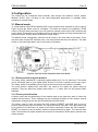
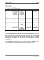
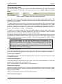
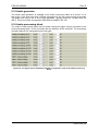
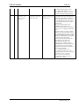
1 Product overview
BYPASS
SDI OUT
SDI OUT
SDI OUT
SDI OUT
Video Test
Generator
SDI
OPTICAL
IN
Reclocker /
De-serialiser
Deglitcher
16 ch Audio
De-embedder
Video Fixed
Delay
SDI
ELECTRICAL
IN
Video
Processing /
Gain /
Label insert
x-point
16 ch Audio
Embedder
Frame Sync
REF
Genlock
Audio Tone
Generator
Tracking Ctrl
Audio x-point
GPI
General Ctrl
Control
Audio
Tracking
Delay
Preset Ctrl
GYDA
4 AES IN
Audio Fixed
Delay
Audio
Processing &
Gain
RS422 Dec
4 AES
Selectable I/O
CTRL
Audio SRC
RS422
OUT
4 AES OUT
Figure 1: Simplified block diagram of the FRS-HD-XMUX4 card
1.1 Product description
The Flashlink FRS-HD-XMUX4 synchronizes an HD-SDI or an SD-SDI input to a reference.
The reference can be a traditional black & burst signal or a tri-level sync. The HD-SDI/SDSDI output can be adjusted relative to the sync signal. The FRS-HD-XMUX4 also has a deglitcher that guarantees error-free synchronous switching.
FRS-HD-XMUX4 can also be used as a frame delay without the reference input. The
adjustable delay is then relative to the input SDI signal.
The audio embedded in the SDI is de-embedded and can be delayed relative to the video.
Each audio stereo pair can also be swapped internally, and the stereo pairs can be routed in
a matrix before being embedded back into the SDI. It is also possible to disable the
embedder function and keep the SDI stream unaltered.
A four output mono mixer is integrated into the stereo router. Each mono output is the sum of
two signals. The sources to the mixer are the same sources as in the stereo router.
A subset of the user-modifiable parameters of the card can be controlled by switches on the
board, all user-modifiable parameters can be controlled from the MULTICON GYDA system
controller.
1.2 Product versions
FRS-HD-XMUX4
SD/HD frame sync, 4AES I/O, 4 SDI outputs
FRS-HD-XMUX4-R
SD/HD frame sync with PIN, 9/125um single mode optical input,
4AES I/O, 4 SDI outputs
FRS-HD-XMUX4-R-L
SD/HD frame sync with APD 9/125um single mode
4AES I/O, 4 SDI outputs
optical input,
nevion.com | 4
FRS-HD-XMUX4
Rev. D
1.3 Key features
4 x HD-SDI outputs
4 x AES I/O
HD/SD video support, including DVB-ASI in through mode
De-glitching of input video signal (always seamless output)
HD/SD frame sync / delay (8 frames max)
Apply sample rate converters on the AES inputs when needed
Make mono mixes of two signals
Luma/chroma gain and level adjustment
Audio delay enabling Dolby-E processing delay correction
Audio router for embedded audio
Embedded audio gain adjustment
Audio fade out/fade in at frame-wrap
SDI in-monitor label inserter
EDH processing
nevion.com | 5
FRS-HD-XMUX4
Rev. D
2 Specifications
Optical SDI input
Data rate optical:
Sensitivity
- SD-/HD-SDI (270/1485
Mbps):
Detector overload threshold:
Detector damage threshold:
Optical wavelength:
Transmission circuit fiber:
Connector return loss:
Connector:
270 – 1485 Mbps
Better than -20dBm (PIN)/-30dBm (APD)
Min. -3dBm
>+1dBm
1200-1620nm
9/125um Single Mode
>40dB w/ SM fiber
SC/UPC
Electrical SDI input
Connectors
Equalization
Input Return loss
Jitter tolerance
75 Ohm BNC
Automatic;
- >300m @270Mbps w/Belden 8281, with BER < 10E-12
- >100m @1485Mbps w/Belden 1694A, with BER < 10E-12
>15dB, 5MHz -1.5GHz
SD limit:
- 10Hz-1kHz: >1 UI
- 10kHz – 5MHz: >0.2 UI
HD limit:
- 10Hz-100kHz: >1 UI
- 100kHz–10MHz: >0.2 UI
Electrical Sync input
Connector
Format
Input Return loss
Termination
75 Ohm BNC
Black & Burst, Tri-level
>35dB @ < 10MHz,
30dB @ < 30MHz
Selectable internal or external 75 Ohm termination
Electrical SDI outputs
Number of outputs
Connectors
Output Return loss
Output signal level
Output signal rise / fall time
20% - 80%
Amplitude overshoot
Output timing jitter
Output alignment jitter
4
75 Ohm BNC
>15dB, 5MHz -1.5GHz
800mV +/- 10%
- SD limit: [0.4ns – 1.5ns] , <0.5ns rise/fall difference.
- HD limit: < 270ps, <100ps rise/fall difference.
<10%
- SD: <0.2 UI
- HD: <1 UI
- SD: <0.15 UI
nevion.com | 6
FRS-HD-XMUX4
Rev. D
- HD: <0.15 UI
AES I/O
Number of inputs/outputs
Connectors
Return loss
Output jitter
Impedance
Input audio data rate
Embedded audio word
length
Embedded audio Channels
status
4
WECO
110R +/-20% 0.1MHz – 6.144MHz
<0.0025UI peak
110 ohm transformer balanced
24 kHz to 100 kHz, converted to 48 kHz uf not isochronous to
either SDI input or sync input.
24 bits
As received when isochronous, otherwise fixed.
Supported standards
SD, 270 Mbps
HD, 1485 Mbps
Video switch point definition
and sync
AES
Optical
EDH
Video Payload Identification
SMPTE 259M, SMPTE 272M-AC
SMPTE 292M, SMPTE 274M, SMPTE 291M, SMPTE 296M,
SMPTE 299M
SMPTE RP168 (tri-level), SMPTE 170m, ITU-R. BT.470
AES3-1996
SMPTE 297M, SMPTE 292M
Compliant to SMPTE-RP165
SMPTE 352M-2002
Other
Power consumption
GPI I/O
+5 VDC / 5 W max
4 inputs
1 output - open drain max. 35 V/150 mA
nevion.com | 7
FRS-HD-XMUX4
Rev. D
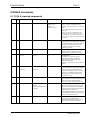
3 Configuration
The board can be configured both manually and through the Network control system
Multicon GYDA. Only a subset of the user-configurable parameters is available when
operating in manual mode.
3.1 Manual mode
To reach manual mode DIP24 labelled OVR on the board must be switched on (to the right in
Figure 2) and the board must be re-booted. This takes the board out of Multicon GYDA
control (if the DIP was previously set to off) and into manual control by the DIP switches and
rotary switch. Parameters not controlled by any of these switches are kept unchanged from
previous session (factory default or Multicon GYDA setup).
The Manual mode configuration controls are all found on the front side of the board. There
are three sets of eight DIP switches each, one rotary switch and two push buttons. The slide
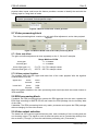
switch on the lower right side is set for all modes of operation.
Figure 2: Top view of the component side of the board.
3.1.1 Rotary switch and push buttons
The rotary switch, labelled DLY, adjusts the phase delay from -5 to +4 video lines. The switch
is only functional when a sync signal (black & burst or tri-level) is present at the sync input.
The rotary switch is accessible from the front of the frame when the module is installed.
The push buttons, labelled INC and DEC, are used to fine adjust the phase delay by
samples. They can adjust the phase delay within +/- ½ video lines for the present video
standard.
3.1.2 Factory reset function
A factory reset sets all parameters of the module back to the state they were in when the
module left the factory. These settings are just a starting condition for the module, and all
subsequent changes by the user will still take effect and be stored.
The factory reset is done by setting the DIP marked F-RESET and OVR both to the on
position, and powering up the module. The inputs should be removed. Then the module has
to be pulled out of the frame (or power to the frame removed), before the DIP marked FRESET is put back to the off position and the module powered up again. The card will then
reset. The board must remain powered for at least 10 seconds for all the factory values to be
stored properly.
nevion.com | 8
FRS-HD-XMUX4
Rev. D
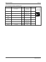
3.1.3 DIP switch functions
Note that the left DIP switch of the horizontal DIP package is number 1. The top
DIP switch of the vertical DIP package is number 17.
Switch #
1
Function name
AES1 dir
Function DIPs
Off = input
On = output
2-4
AES1/GRP 1
routing
DIP
234
Group 1
Embeddin
g
000
Disable
001
Group 1
010
Group 2
011
Group 3
100
Group 4
101
AES1&2
110
AES3&4
111
Generator
AES1
output
Deembed
ding
Group 1
ch 1&2
Group 1
ch 3&4
Group 2
ch 1&2
Group 2
ch 3&4
Group 3
ch 1&2
Group 3
ch 3&4
Group 4
ch 1&2
Group 4
ch 3&4
5
AES2 dir
Off = input
On = output
See table for AES1/GRP1
6-8
AES2/GRP2
9
AES3 dir
10-12
13
AES3/GRP 3
AES4 dir
14-16
AES4/GRP 4
X- Y
Frame delay
DIP[1 2] = [Off Off ] => 0 frms
DIP[1 2] = [Off Off ] => 1 frms
DIP[1 2] = [Off On ] => 2 frms
DIP[1 2] = [Off On ] => 3 frms
ADLY
Audio follows
video delay
On: De-embedded audio
follows video. DIP 17-18 is
used
Off: De-embedded audio will
not use Frame delay from dip
17-18
OPT/EL
OPT/EL
Off = input
On = output
See table for AES1/GRP1
Off = input
On = output
See table for AES1/GRP1
Comment
AES 1 input or output, if
AES1 is input, DIP 2-4
routes GROUP 1.
Routing matrix to AES1 or
GROUP 1
Aes 2 input or output
Routing Matrix to AES2 or
GROUP 2
AES 3 in or out
Routing AES3 / GROUP 3
AES 4 in or out
Routing matrix AES4 /
GROUP 4
With a sync-input present,
this sets the minimum
frames delay.
Without a sync-input
present this sets the no. of
frames delay relative to the
input.
If on, de-embedded audio
delay will follow video delay
Optical / Electrical input
nevion.com | 9
FRS-HD-XMUX4
Rev. D
SDO1PR
OC
SDI OUT 1
Off: through mode
On: processed mode
SDO2PR
OC
SDI OUT 2
Off: through mode
On: processed mode
F-RESET
F-RESET
Off: Use values preset by
MULTICON GYDA.
On: RESET to factory defaults
OVR
OVR
Off: MULTICON GYDA mode
On: Manual mode
In through mode the video
only goes through a reclocker.
In through mode the video
only goes through a reclocker.
This DIP is only read at
power up. After repowering
with the DIP off, the board
must be kept in the frame
for minimum 10s to fully
reset.
Values preset by
MULTICON GYDA, are only
values not set by DIPs,
push buttons or rotary
switches.
This DIP is only read at
power up.
OVR is short term for
MULTICON GYDA override
Table 1: DIP SWITCH FUNCTIONS
3.2 Multicon GYDA mode
All functions of the card can be controlled through the Multicon GYDA control system. The
Multicon GYDA has an information page and a configuration page.
3.2.1 Information page
The information page shows a dynamic block-diagram of the board and some additional
information text. The block diagram updates with the board status, showing input signal
selected and signals missing (by red crosses over signal lines). It also shows the audio
matrix selections that have been made in the configuration page.
Note that if an audio input is not present, the user will still be allowed to select the
input in the matrix, but the output logic will immediately select the fallback
generator as specified by the user. The missing signal source will be shown in
the block-diagram with a red cross over the input line to the matrix.
The text on the information page gives information about functionality not displayed on the
dynamic block diagram.
The video delay presents the calculated actual delay between input and output video.
3.2.2 Configuration page
The different configuration possibilities are explained in detail in Chapter 5, under the
corresponding functions.
nevion.com | 10
FRS-HD-XMUX4
Rev. D
Figure 3: Multicon GYDA information page
3.3 Connections
Figure 4: FRS-HD-XMUX4-C1 backplane
left: connection side
right: component side
nevion.com | 11
FRS-HD-XMUX4
Rev. D
The backplane for the FRS-HD-XMUX4 is labeled FRS-HD-XMUX4-C1. The table below
shows the connectors and their functions.
Function
HD/SD-SDI input
HD/SD-SDI output 1
HD/SD-SDI output 1 inverted
HD/SD-SDI output 2
HD/SD-SDI output 2 inverted
Black & Burst/ tri-level input
AES I/O 1
AES I/O 2
AES I/O 3
AES I/O 4
GPI in
GPI out
DATA out
Label
IN
1
_
1
2
_
2
SYNC
1
2
3
4
GPI/DATA
GPI/DATA
GPI/DATA
Connector type
BNC
BNC
BNC
BNC
BNC
BNC
WECO
WECO
WECO
WECO
TP45, pin 2, 3, 6 & 7
TP45 pin 1 (pin 8 = GND)
TP45 pin 4 & 5
Table 2: Connector functions
Unused SDI-inputs/outputs must be terminated with 75 Ohm.
3.4 Sync input
The backplane also features a switchable termination. By setting the slide switch in Figure 4
to on the sync input will be terminated to 75 Ohm.
nevion.com | 12
FRS-HD-XMUX4
Rev. D
4 Operation
4.1 Front panel LED indicators
Diode \ state
Card status
Red LED
PTC fuse has
been triggered
or FPGA
programming
has failed
SDI input status
Video signal
absent.
Sync input
status
Sync signal
absent
Audio input
status
No audio
embedded in
incoming video
Orange LED
Module has not
been
programmed,
RESET and
OVR DIPS are
on or module is
loading new
firmware.
Video signal
present but card
not able to lock
VCXO
Sync signal
present but card
unable to lock
VCXO
One, two or
three audio
groups
embedded in
incoming video
Green LED
Module is OK
No light
Module has no
power
Video input
signal in lock
Module has not
been
programmed
B&B or Tri-level
sync in lock
Module has not
been
programmed
4 audio groups
embedded in
incoming video
Module has not
been
programmed
Special conditions for the LEDs
The locate command will make all lights blink on and off synchronously, before they return to
their normal functions as described above.
An FPGA firmware upgrade will activate running lights on the LEDs after the download is
finished. Do not remove power to the card when the running lights are active, the card is
busy unpacking and installing the new firmware. The FRS-HD-XMUX4 will reboot
automatically when finished.
4.2 GPI alarms
The FRS-HD-XMUX4 has one GPI output only. This is the status of the module, and it
follows the same logic as the Card Status LED described in the previous section.
nevion.com | 13
FRS-HD-XMUX4
Rev. D
4.2.1 Functions of 8pin modular jack
GPI name
Status
Function
General error status for
the module.
Pin #
Pin 1
GPI 1
Reserved for future use
GPI 2
Reserved for future use
DATA-link
output
DATA-link
output
GPI 3
RS422+
Mode
Direction
Inverted Open
Output
Collector
(open is alarm)
Pin 2
TTL, 0V =
Input
active level
Pin 3
TTL, 0V =
Input
active level
Pin 4
RS422
Output
RS422-
Pin 5
RS422
Output
Reserved for future use
Pin 6
Input
GPI 4
Reserved for future use
Pin 7
Ground
0 volt pin
Pin 8
TTL, 0V =
active level
TTL, 0V =
active level
0V.
input
nevion.com | 14
FRS-HD-XMUX4
Rev. D
5 Functional description
5.1 Data path
HD/SD-SDI input is selected from either optical or electrical input and equalized, re-clocked
and de-serialized and transferred to a processing unit called an FPGA. In the FPGA the
signal is first sent through a de-glitcher that cleans up errors that might appear on the video
lines, for instance due to switching. After the video is de-glitched, it is sent along two different
paths; it is sent to a frame-store buffer, and to the audio de-embedder.
The 16 audio channels coming from the de-embedder are bundled in pairs and sent to an
audio buffer. The audio is fetched from the audio buffer according to a user specified delay
and sent to an Audio cross point. The audio from the Audio cross point can be any pair of
audio channels de-embedded from the incoming video stream, AES inputs, an internal 1 kHz
sine or a muted signal. “Muted signal” means that even though there’s silence, there’s still a
legal audio stream present, which makes it different from Delete (for embedded channels)
and Outputs Off (for AES outputs). As part of the Audio cross point, there are also four mono
shuffler outputs that are the result of the users’ choice of signals from the 16 de-embedder
channels and left and right channels from the four AES inputs. From the cross point outputs
each channel pair enters an Audio Processing Block, where the paired channels may be
shuffled. After the audio processing block the audio enters the Audio Embedder.
The video (with audio still inserted) is fetched from the frame buffer with the user specified
delay and sent to a Video processing block followed by an EDH processing block. After the
EDH block the video and audio is embedded according to the user settings and the video is
sent from the FPGA to a serializer that re-clocks the data and output the SDI to a buffered
output switch.
The buffered output switch is a 2x2 cross point with input 1 being the equalized and reclocked input (non-processed) and input 2 being the output of the video processing. The two
outputs are then sent to two paired sets (non-inverting and inverting) of outputs.
There are also 4 I/O ports for AES. These can be setup to be either inputs, outputs or a mix.
The outputs are taken from the Audio cross point and can be any stereo pair of audio
channels embedded on the incoming video stream, the four mono shuffler outputs, the
internal 1 kHz sine generator or the internal “black sound” generator. The inputs are routed
through optional audio delay and sample rate converter before it goes to the audio
crosspoint.
5.2 Video input selection
The FRS-HD-XMUX4 has one electrical and one optical input. The input can be chosen
either by an automatic selection with priorities and rule of switching, or by manual selection.
Manual selection mode
Figure 5: Multicon GYDA view of electrical input selected in manual mode.
nevion.com | 15
FRS-HD-XMUX4
Rev. D
Automatic selection mode
Figure 6: Multicon GYDA view of the input selection
If the Video in mode selector is set to auto in Multicon GYDA, three input choices can be
made for each of the three priority levels: electrical, optical, mute or generator. When the
selected signal on the Main level is lost, the change over will switch to the signal selected on
the next priority level (backup 1) and so on. If the third priority level is not needed, backup 2
can be set to ‘–‘.
The switching between these priority levels is controlled by rules.
The available rules are:
Lol = loss of lock
Los = loss of signal
Hold time and lock time for the signals can also be set.
When using the rule loss of signal, switching function can be selected as either latched or
non-latched.
Non-latched switching function is only possible with rule loss of signal.
5.3 De-glitcher
The de-glitcher corrects timing errors within a single video line. The de-glitcher has a 2048
samples buffer. When the first signal is present, we call it the “initial phase signal”, data is
taken from the centre of this buffer. If the timing reference of the video signal changes, when
for instance a new source being switched into the signal path, the timing errors occurring by
this change will be corrected if the new timing reference is within +/-1024 samples of the
“initial phase signal”. This also goes for all consecutive timing references.
If a signal is more than +/-1024 samples off relative to the “initial phase signal”, the output will
repeat the last frame, refill the 2048 samples buffer and take out data from the centre of the
buffer. This new signal is now considered the “initial phase signal”. Audio will fade out when
a frame repeat is being done, and fade in at the new frame.
Hence, it produces an error free video output without frame wrapping when the video input
comes from a router with synchronous input video signals that all lies within +/-1024 samples
of each other.
The de-glitcher output is always seamless. When a signal is repeated the audio is
faded out. It fades in at the new frame.
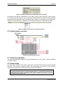
5.4 Frame synchronizer
The frame synchronizer consists of a frame store buffer and some control logic. The frame
store buffer can store up to 8 full HD frames. Data is fetched from this buffer according to the
user settings by force of the control logic. The control logic sets the frame synchronizer into
different modes dependent on the presence of a sync input.
nevion.com | 16
FRS-HD-XMUX4
Rev. D
5.4.1 Frame sync mode
If a sync input (B&B or Tri-level) is present, the frame synchronizer will output a signal that
has a delay relative to this signal. Two parameters can be set: "Phase delay" and "Frame
delay".
Figure 7: Multicon GYDA view of the video delay settings
Let us first focus on the phase delay, which also may be called “output phase delay”. This
parameter can be positive or negative, and determines the relationship between the outgoing
video and the sync signal.
The phase delay can thus be written in several ways, a large positive delay will equal a small
negative delay, because there is wrap-around on a frame basis. It follows that it is not useful
to specify a phase delay larger than 1 frame. Strictly speaking the range could have been
limited to -1/2 frame to 1/2 frame. For convenience, the delay range is allowed to be from -1
frame + 1100 samples to 1 frame – 1100 samples.
In addition to the phase delay, the user may specify additional frames delay. When frame
delay is set to 1 frame, the delay through the card will be between 1 and 2 frames,
depending on the input phase between SDI-input and sync input.
The frames and lines are measured in units of the output SDI video standard. If the output
SDI standard is 1080i25, a delay of one line is equal to 35.5us. If the output SDI standard is
720p50, a delay of one line is equal to 26.6us. If the output SDI standard is 625i25, a delay
of one line is equal to 64us.
For a scenario where the card receives different HD video standards, (e.g.
1080i25 and 720p50) the user may want to conserve a specific delay in
microseconds for all HD video standards. This is accomplished by specifying the
delay in number of samples instead of frames and lines. (For HD video standards
the sample frequency is equal over standards, but the line and frame frequencies
are different for the different standards).
If video input disappears
Given that stable SDI input and sync input exists: If the SDI input disappears, the picture will
freeze for <hold time> and then go to video generator if the card is in default configuration.
If video input reappears
Given stable sync input, the video will reappear after <lock time> of locked video input if card
is in default settings.
If sync input disappears
Given that stable SDI input and sync input exists: If the sync signal disappears, the card will
act as in frame delay mode, see Chapter 5.4.2.
NOTE: This will result in a frame roll as the delay changes.
If sync input reappears
Given that a stable SDI input exists: If the sync signal reappears the delay mode will change
back to Frame Sync mode. Hence the internal clock will be locked to the sync signal and the
delay will again change.
NOTE: This will result in a frame roll as the delay changes.
If both signals disappears
nevion.com | 17
FRS-HD-XMUX4
Rev. D
The picture will first freeze for <hold time> and then go to video generator. The output is now
referenced to the local clock source. However, this clock source will be kept within 1 ppm of
the last sync source.
5.4.2 Frame delay mode
In this mode a sync signal is not present. The phase delay will now be relative to the SDIinput. The phase delay + additional frame delay together set the total video delay.
If video signal disappears
The picture will first freeze <hold time> and then go to video generator. The output is now
referenced to the local clock source. However, this clock source will be kept within 1 ppm of
the last video source.
If video signal reappears
If the input video signal reappears, the video will reappear on the output <lock time> after
stable input video. The delay will be set to the same delay as before loosing input.
NOTE: This may cause a frame roll.
If a sync input appears
Given that a stable SDI input exists: If a sync signal appears the delay mode will change to
Frame Sync mode, see Chapter 5.4.1. Hence the internal clock will be locked to the sync
signal and the delay will again change.
NOTE: This will result in a frame roll as the delay changes.
5.5 Video generator
The video generator can produce several simple signals: Color bar, Check field and Flat
field.
The flat field feature is controlled by setting the luma and chroma values (each is a 10bit
value, 0-1023), or by selecting one of the pre-defined colors (black, white, yellow, cyan,
green, magenta, red, or blue).
By default the generator is selected as the video source if there is no video signal present at
either of the video inputs. The video standard will then be determined by the legal video input
last seen by the card. The Video format selector has no effect in this mode.
The generator may also be forced on from Multicon GYDA by selecting the video generator
as main input in Video in. The video standard is then determined by the Video format
selector. This selector will override video input but the internal generator will still be locked to
the input signal. In other words: For correct generator output in this mode, the input must
either be missing or the input must be of the same frequency base as the selected output
standard.
Figure 8: Multicon GYDA view of the video generator
5.6 Label generator
The label generator consists of 2 lines of 16 characters each that are placed at the lower left
corner of the active area.
The “On” tick-box will show the label at all times, while the “Off” will turn the label generator
off at all times. If “Auto” is ticked, the label will be shown as an overlay on the internal video
generator only. Typically, the internal video generator will be used as a fallback for the
nevion.com | 18
FRS-HD-XMUX4
Rev. D
physical video inputs, and hence this feature provides a means to identify the card with the
missing input in a long chain of cards.
Note that in order to see the label on an output, the video output selection must
be set to “processed” for that specific output.
Figure 9: Multicon GYDA view of label generator
5.7 Video processing block
The video processing block consists of a gain and offset adjustment, and a video payload
legalizer.
Figure 10: Multicon GYDA view of the video processing block
5.7.1 Gain and offset
The gain and offset adjustment is done separately on the Y, Cb and Cr samples.
Luma gain
Chroma gain
Luma offset (gain =1)
Chroma offset (gain = 1)
Range Multicon GYDA
0 – 3.999999
0 – 3.999999
511.75 – 511.75 in sample values
255.75 – 255.75 in sample values
5.7.2 Video payload legalizer
The legalizer hard clips the upper and lower limit of the video payload. With the legalizer
enabled these limits are:
Upper limit
Luma:
Chroma:
Lower limit
Luma:
Chroma:
With the legalizer disabled,
3FBh and 004h.
3ACh
3C0h
040h
040h
the video processing block hard clips both luma and chroma to
5.8 EDH processing block
If enabled, the EDH processing block extracts the EDH package from the video, updates the
EDH flags according to SMPTE RP165 and inserts the EDH package into the ancillary data
of the video.
If disabled, The EDH processing block only reads, processes and reports the EDH package
without changing it in the video stream.
5.9 Video output selection
The board has four outputs organized as two pairs, each consisting of one inverting and one
non-inverting output. The signal to each of these two pairs can be routed either directly from
the re-clocker (“Through”) or from the audio/video processing unit (“Processed”).
nevion.com | 19
FRS-HD-XMUX4
Rev. D
Figure 11: Multicon GYDA view of SDI output selection block
All features that requires modification of the video content (video generator, label overlay,
etc.) requires that the output is set to Processed. Note that when the internal video generator
is selected (either because it was selected as main in Video in, or because it was selected as
fallback for a missing input), outputs set to Through will behave as if Mute was selected.
Figure 12: Multicon GYDA view of video input mode.
5.10 Audio blocks overview
Figure 13: Audio function blocks
5.11 Audio de-embedder
The Audio de-embedder extracts all audio embedded in the video stream. The de-embedder
is always enabled.
5.12 Audio delay
An audio delay relative to the video output can be specified commonly for all de-embedded
channels. This is done in Multicon GYDA. The audio delay is specified in audio samples
relative to the output video, and can be both positive and negative.
Note that as the audio delay is relative to the video output, it’s possible to specify
an audio delay that will be an actual negative delay, i.e. request that audio will be
output before the video containing those audio samples has arrived. This will
inevitably cause audio errors.
nevion.com | 20
FRS-HD-XMUX4
Rev. D
The negative audio delay is limited by the positive video delay. Since the audio delay is
always relative to the video, the only way to give the audio a negative delay is to delay the
video by a positive amount. To go beyond this limit would require the audio to be reembedded before it had even been de-embedded from the incoming video, and that is of
course impossible.
The positive audio delay is limited by the fact that the sum of the video delay and the relative
audio delay cannot be larger than 32000 audio samples (approx. 0.67 ms with 48 kHz audio).
If the video delay is set to minimum, the full 32000 audio samples will be available, but if the
video delay is set to – say – 5 frames, the maximum relative audio delay is reduced to 20000
audio samples (assuming 25 frames per second, 5 frames equals 0.2 seconds, which in turn
equals 12000 audio samples, and 32000-12000=20000). When doing these calculations,
remember that if a sync reference is present, a video delay setting of N frames means that
the actual video delay can vary continuously between N and (N+1) frames. The calculations
should therefore be based on (N+1) frames.
Dolby-E delay handling
The FRS-HD-XMUX4 can re-align Dolby-E with video. Dolby-E processing equipment
typically causes one frame delay for the audio.
The positive video delay needs to be set higher than the wanted negative relative audio
delay. Then set a negative relative audio delay that corresponds to a whole number of full
frames of audio samples1. A delay example setting is shown in Figure 14. The de-embedded
audio can be routed to one or more AES outputs and through a Dolby encoder/decoder and
back in to one or more AES inputs. The delay on the AES inputs should probably be set to
zero, but may be adjusted to align audio with video.
Figure 14: Multicon GYDA view of the delay settings. With these settings, the video is delayed 1
frame relative to the de-embedded audio for a signal with 50 frames per second.
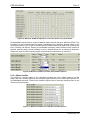
5.13 Audio cross point matrix
The audio cross point matrix is an 18x13 cross point with inputs and outputs as shown in
Figure 13. The four AES inputs, the eight de-embedded channels, 4 mono shuffler channels,
a 1 kHz sine and a muted signal (silence) are selectable inputs. The outputs of the cross
point are the eight stereo channels for re-embedding, four AES outputs, and a separate data
output for data recovered from one of the stereo pairs.
Each AES port is configurable as either an input or an output. Hence not all positions in the
matrix are legal. For example, an AES port configured as an output can’t really function as an
input for embedding, even though the selection can be made in the matrix.
1
To calculate number of audio samples/frame simply divide 48000 with frame rate (24Hz, 25Hz,
29.97Hz, 30Hz, 50Hz, 59.94Hz or 60Hz)
nevion.com | 21
FRS-HD-XMUX4
Rev. D
Figure 15: Multicon GYDA configuration view of the audio cross point matrix
All embedded outputs have a common fallback option that can be set in Multicon GYDA. The
priorities can be selected between matrix (representing the selection already made in the
cross point matrix), sine, mute or delete/output off. Mute means that legal audio is produces,
but it contains just silence. Delete (for embedded channels) means that the audio content is
deleted, and the audio control package is set to channel delete for its respective channels.
Output off (used for AES outputs) simply means that the output driver is turned off.
Figure 16: Multicon GYDA view of the audio fallback options
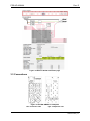
5.13.1 Mono shuffler
The matrix is a stereo matrix so the selection chooses the Left or Right channel. At this
stage, the user chooses between the Left and Right channels of the AES inputs and the 16
de-embedded channels. These mono shuffler outputs can be used by choosing them in the
Audio cross point matrix.
Figure 17: Multicon GYDA view of the Mono shuffler options
nevion.com | 22
FRS-HD-XMUX4
Rev. D
The mono shuffler stereo signals are each made up of two input sources and can use inputs
from both the AES and the de-embedded channels, for example in Figure 17 above, mono
shuffler 1 uses AES input 1L and AES input 1R to make up the mono shuffler 1 output signal,
while mono shuffler 3 output is made up from de-embedded channels 5 and 6. It is important
to note that the correct settings for the AES has to be chosen as inputs and outputs. In this
example AES channels 1 and 2 are set as inputs, while channels 3 and 4 are set as outputs,
as can be seen as part of Figure 18, where the direction of each of the AES ports are
controlled.
In order to choose the desired output channel, the audio cross point matrix is used, see
Figure 15. In this example, mono shuffler 1 signal is placed on the AES 3 channel, the mono
shuffler 2 signal is set on the AES 4 channel, the mono shuffler 3 signal is embedded in the
group 2 ch 5-6 output and the mono shuffler 4 signal is embedded in group 2 ch 11-12 output
channel.
5.14 AES I/O
The direction of the four AES ports can be selected by the user. This means the user has
any combinations of inputs and outputs available: 4 inputs and 0 outputs, 3 inputs and 1
output, 2 inputs and 2 outputs, 1 input and 3 outputs or no inputs and 4 outputs, the setting of
these directions can be seen as part of Error! Reference source not found..
5.14.1 Audio inputs
When an AES I/O port is set to be input, the sample frequency of the input is monitored to
see if the signal is synchronous with the system clock. If not, the audio input is passed
through a sample-rate converter. After the input block the audio can be delayed with
individual delay for each AES port, before it is routed to the audio matrix. The audio delay for
AES inputs are set relative to the AES input port.
If the AES input port is synchronous with the SDI-input, the user can select the AES input
delay to track to the video delay. The card will calculate the relative delay for the audio based
on the delay setting for video and audio. This is useful if the SDI-in and AES has a common
clock source and the sync input has a different clock source.
5.14.2 Sample Rate Converter
This setting can be used to force the sample rate converters to either be set to on, off or to
auto. If track to video is enabled, the sample rate converter should be either set to off or auto
mode.
If the switch is set to off, the sample rate converters will be used as necessary.
Figure 18: Multicon Gyda view of the sample rate converter settings.
5.14.3 Audio outputs
The AES outputs are routed from the audio matrix via individual audio processing blocks.
The outputs are always 48 kHz and synchronous to the system clock. The AES outputs have
individual fallback options, see chapter 5.13.
nevion.com | 23
FRS-HD-XMUX4
Rev. D
5.15 Audio generator
The stereo audio generator is available in the audio cross point matrix as a source. It is a
high purity 1 kHz sine wave with a 250ms interruption on the left channel every 3 seconds.
The audio level may be set to one of two standards. The two levels are -18 dBFS and -20
dBFS. These two levels correspond to EBU R68 and SMPTE RP 155.
5.16 Audio processing block
The output of each stereo signal from the audio cross point matrix may be processed in the
audio processing block. This is controlled with the Multicon GYDA controller. The processing
includes channel L/R manipulation and audio gain.
Figure 19: The figure shows the Multicon GYDA configuration view of the audio processing
block
nevion.com | 24
FRS-HD-XMUX4
Rev. D
Channel L/R manipulation
The stereo signals may be output in one of the following ways:
- LR, Left / Right
- RL, Right/ Left
- LL, Left/ Left
- RR, Right/ Right
- nLR, ØLeft/ Right
- LnR, Left/ ØRight
- MM, (Left + Right)/2
- MS, MS/AB
No change.
Channels are swapped.
Left channel is copied into the right channel.
Right channel is copied into the left channel.
The left channel is phase inverted.
The right channel is phase inverted.
The left and right channels are summed.
The left and right channels are converted from AB stereo
to MS stereo.
The sum products ( (L+R)/2 and MS) are reduced in level by 6 dB to avoid any possibility of
clipping.
Audio gain
Audio gain is a 16 bit value that can be set for each stereo pair going into the audio
processing block. The gain range is set to [+96dB, -96dB] with a gain step of 0.1dB.
Note that non-audio data is ignored and left unchanged by the gain function.
5.17 Audio embedder
Figure 20: Multicon GYDA view of the audio embedders.
The audio embedder can be enabled per group in Multicon GYDA. When a group is disabled
the audio inside that group is removed.
When in SD mode, a 24bit sound signal can be reduced to 20bit through Multicon GYDA
control. This effectively removes the four least significant bits of the signal. The audio control
package is left unchanged, as the bit range is still present.
The audio control package can also be switched on and off in SD mode through Multicon
GYDA control.
The audio embedder can also be switched off altogether. In this mode the audio embedded
in the video input is left completely unaltered.
nevion.com | 25
FRS-HD-XMUX4
Rev. D
6 RS422 commands
6.1 FLP4.0 required commands
Block
Blk
#
Commands
Example
Response
Control
-
-
?
?
product name\
SW rev n.m\
FW rev r.s\
protocol ver 4.0\
Hello command.
Note 1: No other commands will be
available until the card has received this
hello.
Note 2: This command will also enable
checksums.
Note 3: Cards are designed to be hotswappable. To sync with the start of a
new command, the cards will wait for a
<lf> character before looking for a valid
command.
conf
0
-
conf 0
*too long to list*
Configuration settings
Retrieves the card's configurable settings.
Each addressable block is represented by
a single line. Dynamic status may be
included in response, but is usually
reported in info only.
-
-
info
info
*too long to list*
Dynamic status info
Blocks with static settings only will
usually not be included, see conf above.
-
-
chk off
chk off
ok
Checksum off
If issued twice in succession, this
command will disable checksums.
Note: Responses will still have the
checksums appended.
NOTE1: ? command turns the checksum
back on
-
-
locate on <seconds>
locate on 3
ok
locate off
locate off
Card locator
This command will cause all the LEDs to
flash for a user specified number of
seconds. If omitted, the value <seconds>
will be set to a default of 120 seconds.
The flashing can be terminated at any
time with locate off.
-
-
address
address
address <address>
Card address
This command will check and update the
card's current rack and slot address,
which is normally only done at start-up.
-
-
filename
filename frshdxmux4-0151.ffw
filename frshdxmux4-0102.mfw
<name>'.'<extension>
Firmware upgrades
The <name> part must match the card's
hardware and include a revision number,
and the extension must be either 'ffw' for
FPGA firmware or 'mfw' for
microcontroller firmware. After running
this command the board will wait for the
firmware in Intel-hex format.
-
-
fin
fin
ok
Finalize
Finalize the programming of the
microcontroller. See description of the
uC bootloader (separate document).
nevion.com | 26
FRS-HD-XMUX4
misc
0
-
Rev. D
NOT AVAILABLE BY
COMMAND.
ONLY FOUND in Conf
0
prog | fin
' ' | ovr
Misc info
prog if the card is freshly programmed
by the bootloader and the program is still
un-finalized. fin is the normal condition.
ovr if DIP-switch 16 is set to the ON
position and the card is under DIP-switch
control.
Note 1: The info part of misc has
additional functionality when locate is
used: locating <remaining seconds>.
This enables a visible countdown clock
in Multicon GYDA, but is not a required
part of FLP400.
6.2 Normal control blocks
Block
Blk#
Commands
Example
Response
Control
pin
0
on | off
pin 0 on
pin 0 off
cd | ncd
Pin diode for optical input. No control;
only used to report carrier detect or not
carrier detect.
ceq
0
-
ceq 0
cd | ncd
Cable equalizer for electrical input. No
control; only used to report carrier detect
or no carrier detect.
cho
0
pri <k> |
pri <k> <l> |
pri <k> <l> <m>
cho 0 pri 0
cho pri 0 1
cho pri 10 2
size 3 pri k,l,m auto
Video input select
latch <latch_status> t1
<hold time> t2 <lock
pri: a prioritized list of inputs, used when
time> <rule>
change-over is automatic. The list can
have 1, 2 or 3 entries, or levels. Manual
size 5 pri k,l,m man m mode is effectively the same as
latch <latch_status> t1 automatic mode with one priority level
<hold time> t2 <lock
only, but has its own command.
time> <rule>
0 = from electrical input
1 = from optical input
2 = internal video generator
3 = mute
4 = none
pos man <k> |
pos auto
latch on |
latch off|
latch reset
cho 0 pos man 1
cho 0 pos auto
cho 0 latch on
cho 0 latch off
cho 0 latch reset
rule lol |
rule los
t1 <hold_time>
cho 0 rule lol
cho 0 rule los
t2 <lock_time>
The module will always respond with 3
levels, filling in 4=none for the levels not
used.
cho 0 t1 1000
cho 0 t2 1000
latch: <latch_status> can be either on or
off and selects if the change-over is
latching or not, used when change-over is
automatic. Latch on means that if we've
lost our main source and moved on to a
lower priority level, we'll not search to
see if the higher pri's will reappear.
rule: <rule> can be either los or lol,
which means loss off signal or loss of
lock. This determines what triggers an
automatic change-over.
t1 and t2: change-over doesn't happen
immediately, as a precaution against
glitches and unstable signals. The timers
t1 and t2 let the user decide how long (in
ms) we will cling on to a missing input
before we consider it gone and move on
to the next pri level, and how long an
input with a higher priority should be
present before we consider it repaired
and switch back, respectively.
nevion.com | 27
FRS-HD-XMUX4
Rev. D
Note 1: the latch setting only applies to
rule los. Setting rule to lol will also set
latch to on.
Note 2: the card change back to physical
inputs from generators regardless of
latch setting. As a side note, this means
that t2 is important even when rule=lol
and/or latch is on.
Note 3: If we have selected rule=lol and
a 3-level pri list with two physical inputs
on top and a generator at the bottom and
we're in generator mode (lost both
physical inputs) and both physical inputs
reappear at more or less the same time,
which physical input will be chosen is
unpredictable. This again due to having
one reclocker only and having to hunt for
a valid input in the background while the
generator is still selected.
cho
1
size 3 pri k,l auto
size 3 pri k,l man m
No commands available. Included to
show internal status and to update
Multicon GYDA graphics.
cho
2-13
pri <k> |
pri <k> <l>
cho 2 pri 1
cho 5 pri 0 2
size 4 pri k,l
Audio fallback setting
Audio change-over blocks, one cho per
audio output from the audio matrix, mtx
0. No other settings but the priority list.
0 = from audio matrix
1 = sine
2 = AES with silence
3 = mute
Note: Only generators (pri 1, 2 or 3) are
allowed to be set as first and only
priority.
cho
14
pri <k> |
pri <k> <l>
cho 12 pri 1
cho 12 pri 0 2
size 4 pri k,l
Embedded audio common fallback
setting
A short-cut to set change-overs 2-9 all at
once. Will of course not report anything
in info, that's left to the individual cho
blocks.
gpi
0
act |
inact
gpi 0 act
gpi 0 inact
rcl
0
-
rcl 0
lock | lol
Reclocker. No control, only used to
report lock status.
emb
0-3
en | dis
emb 0 en
emb 2 dis
emb 1 acp on
emb 3 acp off
emb 1 use24 on
emb 2 use24 off
(en | dis) use24 (on |
off) acp (on | off) del
(off | (on <del12>
<del34>))
Audio embedder block
en/dis: Enables or disables the
embedding of the group into the ancillary
area.
acp ( on | off )
use24 ( on | off )
del (off | (on <del12>
<del34>))
emb 0 del off
emb 2 del on 54 -432
EDH insert select
This gpi works as a simple 2:1 switch.
inact : EDH off
act : EDH on
acp on/off: This is valid only for SD and
enables the audio control package.
use24 on/off: This is only valid for SD
and selects between 24bit and 20bit
sound.
del off/on delay12 delay34: For each of
the embedder groups the delay bits for
ch1+2 and for ch3+4 can be inserted into
the ACP. The delay value can be positive
and negative and is put directly into the
nevion.com | 28
FRS-HD-XMUX4
Rev. D
ACP as it is written.
Note: To set both delays to 0 would be
the same as turning the delays off. The
response reflects this.
demb
0-3
-
demb 0
demb 2
vprc
0
lglz on |
lglz off
(y | cb | cr) <gain>
<offset>
vprc 0 lglz on
vprc 0 lglz off
vprc 0 y 1.0000 0
vprc 0 cb 1.0000 0
vprc 0 cr 1.0000 0
grp k en
Audio de-embedders
one permanently assigned to each
incoming group, always enabled. No
control available.
Video processing block
Gain and offset are both signed fixed
point numbers. Gain is in 2.13-format,
while offset for Y and the chroma
channels are given in 10.2 and 9.2
respectively.
Gain range is 0 – 3.99, Gain=0x = 0,
Gain=1x = 1.0, Gain~4x = 3.999999
Luma Offset range is -511.75 – 511.75,
Offset=0 = 0
Chroma Offset range is -255.75 – 255.75,
Offset=0 = 0
sync
0
-
sync 0
'lol' | ('lock' ('trilvl' |
'bb' | 'sdi') )
Frequency reference for video output.
Status only, no commands available.
dly
0
<frames>frms
dly 0 2frms
'tgt' <frames> frms
Video delay
This sets the additional video delay of the
card.
In info this block reports back the current
delay in nanoseconds. This will vary with
the incoming video standard.
dly
1
<audio_samples>sps
dly 1 -30sps
'tgt' <audio_samples>
sps
audio delay for deembedded audio
The audio delay is given in audio
samples. Audio delay is always given
relative to video.
dly
2
<audio_samples>sps
dly 1 -30sps
'tgt' <audio_samples>
sps
audio delay for input AES 1
The audio delay is given in audio
samples. Audio delay is always given
relative to input AES 1.
dly
3
<audio_samples>sps
dly 1 -30sps
'tgt' <audio_samples>
sps
audio delay for input AES 2
The audio delay is given in audio
samples. Audio delay is always given
relative to input AES 2.
dly
4
<audio_samples>sps
dly 1 -30sps
'tgt' <audio_samples>
sps
audio delay for input AES 3
The audio delay is given in audio
samples. Audio delay is always given
relative to input AES 3.
dly
5
<audio_samples>sps
dly 1 -30sps
'tgt' <audio_samples>
sps
audio delay for input AES 4
The audio delay is given in audio
samples. Audio delay is always given
relative to input AES 4.
dly
6
<lines>lines
<samples>sps
dly 2 1lines -30sps
'phase' <lines> lines
<samples> sps
Video phase
If lines != 0 the resulting phase will vary
with incoming video standard, see dly 0
above.
vgen
0
cbar |
mcbar |
chkfield |
white |
yellow |
cyan |
green |
magenta |
red |
vgen 0 cbar
video
<lns>/<rate><scan>
wss ( auto| off | ( on
<wss_value> ) ) (cbar |
chkfield | mcbar | white
| yellow | cyan | green |
magenta | red | blue |
black | (flat <Y> <Cb>
<Cr>) )
Internal video generator.
The video generator will be activated in
two different ways: If selected as a
fallback option the generator will
generate the selected pattern when the
other input(s) are missing, and then use
the video settings from the last external
source present. It can also be selected as
the main input in cho 1, in which case its
vgen 0 flat 200 0 100
vgen 0 video 1080/24p
vgen 0 video 1080/25p
nevion.com | 29
FRS-HD-XMUX4
blue |
black
video
<lns>/<rate><scan>
vgen 0 video 1080/25i
vgen 0 video 1080/29i
vgen 0 video 1080/30i
vgen 0 video 720/24p
vgen 0 video 720/25p
vgen 0 video 720/29p
vgen 0 video 720/30p
wss (auto|off | (on
<wss_val>) )
vgen 0 wss auto
vgen 0 wss on 7
msk <16b_mask>
vmon 0 msk 0xFFFF
reset
vmon 0 reset
<i1> <o1> ...<iN>
<oN>
<i1>
<o1>,<o2>,...<oN>
<i1> <o1> - <o2>
mtx 0 0 2 1 4 5 5
mtx 0 0 0, 1 1, 2 2
mtx 0 0 0-9
flat <Y> <Cb> <Cr>
vmon
mtx
0
0
Rev. D
own video settings will also be used.
msk <16b_mask>
Video monitoring.
Error counting. The count itself is
reported in info. Errors can be masked
off and not counted; this is the purpose of
the mask. The counter itself is 16b and
will wrap around, but can also be reset by
issuing reset.
size M:N i1 i2 i3... iN
Audio matrix
mtx 0 (size 14:13) controls the audio
matrix; outputs 0-7 are embedded sound;
outputs 8-11 are AES output 1 to 4;
output 12 is datalink;
inputs 0-3 are AES inputs,
inputs 4-11 are deembedded sound;
12=1kHz sine, 13=Black/silence
mtx 0 0 0 1 1 2 2-7
..or the above
combined
Note: Any combination of the three basic
commands are allowed, for instance the
following command to set up a 10x10
audio matrix in a single line:
mtx 0 1 1 2 2 3 0,3-7
=> mtx 0 size 10:10 3 1 2 3 3 3 3 3 3
mtx
1
<i1> <o1> ...<i2>
<o2>
<i1> <o1>,<o2>
mtx 1 0 0 1 1
mtx 1 0 0,1
size M:N i1 i2 i3... iN
Video output matrix
mtx 1 (size 2:2) controls the video output
switches.
0: Through mode (re-clocked only)
1: Processed mode (SDI from FPGA
mtx
2
<i1> <o1>
mtx 2 0 0
mtx 2 1 0
size M:N i1 i2 i3... iN
Audio embedder bypass
0: Embedding disabled
1: Embedding enabled
agen
0
lvl <sine_level>cBFS
agen 0 lvl -180
agen 0 lvl -200
sine 1kHz lvl
<sine_level>cBFS
Audio generator
The amplitude of the generated sine that
can be chosen as fallback in audio
change-overs. Legal values are -180cBFS
or -200cBFS (centiBel referred to full
scale output). Units are optional, but if
included must be written as cBFS (case
sensitive).
ablk
0-3
dir in | out
track none | video
ablk 0 dir in
ablk 0 track video
dir in | out
track video | none
AES I/O port 1-4
dir in | out sets the direction of the AES
I/O.
track selects whether AES delay tracks
the video delay.
aprc
0-11
lr |
rl |
ll |
rr |
nlr |
lnr |
mm |
ms |
lvl <gain>
aprc 0 lr
aprc 3 ll
aprc 6 mm
aprc 7 lvl -400
lr |
rl |
ll |
rr |
nlr |
lnr |
mm |
ms
Audio processing
one block for each output from cho 2-13.
The meaning of the commands are as
follows:
lr = Normal
rl = Channel swapped
ll = Left channel to both output channels
rr = Right channel to both output
channels
nlr = Left channel phase inverted
nevion.com | 30
FRS-HD-XMUX4
Rev. D
lnr = Right channel phase inverted
mm = Mono, both channels = (r+l)/2
ms = Mono/stereo, m=(l+r)/2, s=(l-r)/2
lvl means level and is the gain setting.
supr
0
en | dis | auto
lb <page> <L1>
<L2>…<L16>
font <tag>
supr 0 auto
supr 0 lbl 0 65 66 67 0
supr 0 font 1252
Supr 0 en font 0x4e4
Label generator
lb 0 86 73 68 69 79 10 A label generator can be superimposed
76 65 66 69 76
on the video. The setting ‘en’ means it is
always superimposed, ‘dis’ means it is
never superimposed, and ‘auto’ means it
is superimposed on the internal video
generator only.
The text in the label can be set or
modified by the lb <page> subcommand, where page is 0 to operate on
letters 1-16 or 1 to operate on the letters
17-32.
The letters follow as a string of ASCII
numbers. To write more than 16 letters,
two commands must be issued. A string
is always terminated at an ASCII 0, and
ASCII 10 is linefeed/new line. Only the
first ASCII 10 will be honored.
In the second example command, the
label string is set to ‘ABC’ and
terminated with ASCII 0. If not
terminated, the command would’ve
modified the first 3 letters of the string,
but any remains of a previous string
would still be present (until ASCII 0 or
33rd letter encountered).
Note 1: When the flash is busy
programming the FPGA or is being
programmed with new FPGA code, label
information can not be updated.
Note 2: At the present, only one
font/codepage (codepage 1252) is
included in the module.
nevion.com | 31
FRS-HD-XMUX4
Rev. D
6.3 Commands intended for debug/lab use only
Block
Blk
#
Commands
example
Response
Control
spi
-
on | off
spi on
spi off
spi off used to isolate the uC from the
SPI lines during programming of the
flash by external programmer. spi on
must be issued in order to re-enable
normal card operation with the uC as the
SPI master.
spir
-
<address>
spir 0x0004
Read a single word (or byte) from a SPI
registers. Addressing is 16b and most
significant nibble determines which chip.
These are the address ranges:
0x0000 – 0x0fff : AES dir and SRC
0x1000 – 0x1fff : FPGA
0x2000 – 0x2fff : flash
0x3000 – 0x3fff : deserializer
0x4000 – 0x4fff : serializer
0x5000 – 0x5fff : shift register for LEDs
0x6000 – 0x6fff : F-RAM
0x7000 – 0x7fff : Rotary switches
spiw
-
<address> <data>
spiw 0x0004 0x2c
With the same address ranges as for spir
above, this command allows the user to
modify SPI registers.
thebug
-
-
thebug
A collection of debug information that is
presented in a Multicon GYDA blocklike format. First line tells which image
is currently loaded. Second line contains
the filename and version of the uC
software, including the AVR controller it
was compiled for. The third line contains
the SW flags in uC, the number of times
the watchdog timer has kicked in,
readout of dip-switches, input select for
deserializer, SDOn on/off, slew rates,
and status for the video changeovers.
The next two lines contain raster
information from the deserializer and
serializer respectively, while the next two
lines contain sample values for mlines
and VCXO.
nevion.com | 32
FRS-HD-XMUX4
Rev. D
General environmental requirements for Nevion equipment
1.
2.
-
The equipment will meet the guaranteed performance specification under the following
environmental conditions:
Operating room temperature range:
0°C to 45°C
Operating relative humidity range:
<90% (non-condensing)
The equipment will operate without damage under the following environmental
conditions:
Temperature range:
-10°C to 55°C
Relative humidity range:
<95% (non-condensing)
nevion.com | 33
FRS-HD-XMUX4
Rev. D
Product Warranty
The warranty terms and conditions for the product(s) covered by this manual follow the
General Sales Conditions by Nevion, which are available on the company web site:
www.nevion.com
nevion.com | 34
FRS-HD-XMUX4
Rev. D
Appendix A Materials declaration and recycling information
A.1 Materials declaration
For product sold into China after 1st March 2007, we comply with the “Administrative
Measure on the Control of Pollution by Electronic Information Products”. In the first stage of
this legislation, content of six hazardous materials has to be declared. The table below
shows the required information.
Toxic or hazardous substances and elements
組成名稱
Part Name
FRS-HD-XMUX4
鉛
汞
镉
六价铬
多溴联苯
多溴二苯醚
Lead Mercury Cadmium Hexavalent Polybrominated Polybrominated
(Pb)
(Hg)
Chromium
biphenyls
diphenyl ethers
(Cd)
(Cr(VI))
(PBB)
(PBDE)
O
O
O
O
O
O
O: Indicates that this toxic or hazardous substance contained in all of the homogeneous materials for
this part is below the limit requirement in SJ/T11363-2006.
X: Indicates that this toxic or hazardous substance contained in at least one of the homogeneous
materials used for this part is above the limit requirement in SJ/T11363-2006.
This is indicated by the product marking:
A.2 Recycling information
Nevion provides assistance to customers and recyclers through our web site
http://www.nevion.com/. Please contact Nevion Customer Support for assistance with
recycling if this site does not show the information you require.
Where it is not possible to return the product to Nevion or its agents for recycling, the
following general information may be of assistance:
Before attempting disassembly, ensure the product is completely disconnected from
power and signal connections.
All major parts are marked or labeled to show their material content.
Depending on the date of manufacture, this product may contain lead in solder.
Some circuit boards may contain battery-backed memory devices.
nevion.com | 35