1
HUNT ENGINEERING
Chestnut Court, Burton Row,
Brent Knoll, Somerset, TA9 4BP, UK
Tel: (+44) (0)1278 760188,
Fax: (+44) (0)1278 760199,
Email: sales@hunteng.co.uk
http://www.hunteng.co.uk
http://www.hunt-dsp.com
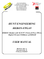
HUNT ENGINEERING
HERON-FPGA9
HERON Module with XC2VP7 (Virtex-II Pro) FPGA,
Digital I/O and 256Mbytes of SDRAM
USER MANUAL
Hardware Rev A
Document Rev D
P.Warnes 03/08/05
COPYRIGHT
This documentation and the product it is supplied with are Copyright HUNT
ENGINEERING 2004. All rights reserved. HUNT ENGINEERING maintains a policy
of continual product development and hence reserves the right to change product
specification without prior warning.
WARRANTIES LIABILITY and INDEMNITIES
HUNT ENGINEERING warrants the hardware to be free from defects in the material
and workmanship for 12 months from the date of purchase. Product returned under the
terms of the warranty must be returned carriage paid to the main offices of HUNT
ENGINEERING situated at BRENT KNOLL Somerset UK, the product will be repaired
or replaced at the discretion of HUNT ENGINEERING.
If HUNT ENGINEERING decides that there is any evidence of
electrical or mechanical abuse to the hardware, then the customer shall have no
recourse to HUNT ENGINEERING or its agents. In such circumstances HUNT
ENGINEERING may at its discretion offer to repair the hardware and charge for
that repair.
Exclusions -
Limitations of Liability - HUNT
ENGINEERING makes no warranty as to the fitness of
the product for any particular purpose. In no event shall HUNT
ENGINEERING’S liability related to the product exceed the purchase fee actually
paid by you for the product. Neither HUNT ENGINEERING nor its suppliers
shall in any event be liable for any indirect, consequential or financial damages
caused by the delivery, use or performance of this product.
Because some states do not allow the exclusion or limitation of incidental or consequential
damages or limitation on how long an implied warranty lasts, the above limitations may not
apply to you.
TECHNICAL SUPPORT
Technical support for HUNT ENGINEERING products should first be obtained from the
comprehensive Support section http://www.hunteng.co.uk/support/index.htm on the
HUNT ENGINEERING web site. This includes FAQs, latest product, software and
documentation updates etc. Or contact your local supplier - if you are unsure of details
please refer to http://www.hunteng.co.uk for the list of current re-sellers.
HUNT ENGINEERING technical support can be contacted by emailing
support@hunteng.demon.co.uk, calling the direct support telephone number +44 (0)1278
760775, or by calling the general number +44 (0)1278 760188 and choosing the technical
support option.
Version
A
initial document
B added appendix 3
C updated ‘How to Make a New Design’ section to reference external document
D deleted erroneous text in ‘Important!’ section. Revised Example3 reference, as example changed
2
HUNT ENGINEERING HERON-FPGA9 USER MANUAL
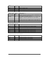
TABLE OF CONTENTS
INTRODUCTION.......................................................................................................... 6
PHYSICAL LOCATION OF ITEMS ON THE HERON-FPGA9............................ 8
GETTING STARTED ................................................................................................... 9
STANDARD INTELLECTUAL PROPERTY (IP) ............................................................................................. 9
MODULE FEATURES ............................................................................................... 10
USER PROGRAMMABLE FPGA WITH EMBEDDED POWER PC ................................................................ 10
SERIAL CONFIGURATION OF THE USER FPGA ....................................................................................... 10
USER FPGA BOOT ROM ..................................................................................................................... 10
CLOCKING OF THE FPGA ...................................................................................................................... 12
HERON FIFOS .................................................................................................................................... 13
DDR SDRAM ...................................................................................................................................... 14
FLASH MEMORY ................................................................................................................................. 14
DIGITAL I/O........................................................................................................................................... 15
MODULE AND CARRIER ID .................................................................................................................... 15
GENERAL PURPOSE LEDS ..................................................................................................................... 15
DONE LEDS .......................................................................................................................................... 15
USB ...................................................................................................................................................... 15
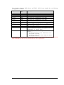
GETTING STARTED ON YOUR FPGA DESIGN ................................................. 17
WORKING THROUGH EXAMPLE 1........................................................................................................... 18
Preparing ISE .................................................................................................................................. 18
Copying the examples from the HUNT ENGINEERING CD........................................................... 19
Opening the Example1 Project........................................................................................................ 19
The Project's Functional Parameters .............................................................................................. 19
Setting up the Configuration Package............................................................................................. 20
User Timing Constraints.................................................................................................................. 21
Creating the Bitstream for Example1 .............................................................................................. 22
Simulating the Complete Design ..................................................................................................... 23
MAKING YOUR OWN FPGA DESIGN................................................................... 24
USER_AP INTERFACE ............................................................................................................................ 24
HARDWARE INTERFACE LAYER ............................................................................................................. 29
IMPORTANT!.......................................................................................................................................... 29
OTHER EXAMPLES ................................................................................................................................. 30
HOW TO MAKE A NEW DESIGN ............................................................................................................. 30
Inserting your own Logic................................................................................................................. 31
Top-level Fine Tuning (using other special IO pins)....................................................................... 31
User Timing Constraints.................................................................................................................. 31
HINTS FOR FPGA DESIGNS ................................................................................................................... 32
Use of Clocks ................................................................................................................................... 32
Possible Sources of Clocks .............................................................................................................. 33
Flow Control.................................................................................................................................... 33
Pipeline Length or “latency” .......................................................................................................... 34
I/O FROM THE FPGA............................................................................................................................. 34
DSP WITH YOUR FPGA......................................................................................................................... 34
SOFTWARE................................................................................................................. 35
FPGA DEVELOPMENT TOOL.................................................................................................................. 35
DESIGN FILES FOR THE FPGA ............................................................................................................... 35
GENERATING DESIGN FILES................................................................................................................... 36
Files for HERON Utility (*.rbt) ....................................................................................................... 36
Files for PROMs (*.mcs) ................................................................................................................. 37
3
HUNT ENGINEERING HERON-FPGA9 USER MANUAL
POWER PC SOFTWARE........................................................................................................................... 37
HERON_FPGA CONFIGURATION TOOL ............................................................................................... 37
HUNT ENGINEERING HOST-API.................................................................................................... 37
HUNT ENGINEERING HERON-API................................................................................................. 37
HARDWARE DETAILS ............................................................................................. 38
HERON MODULE TYPE ........................................................................................................................ 38
HARDWARE RESET ................................................................................................................................ 38
SOFTWARE RESET (VIA SERIAL BUS)..................................................................................................... 38
CONFIG.................................................................................................................................................. 38
DEFAULT ROUTING JUMPERS ................................................................................................................ 39
PHYSICAL DIMENSIONS OF THE MODULE .............................................................................................. 39
POWER REQUIREMENTS OF THE HERON-FPGA9................................................................................. 40
FPGA POWER CONSUMPTION/DISSIPATION .......................................................................................... 40
Choosing an Appropriate Heatsink and Fan................................................................................... 41
How the Power Limit is Calculated ................................................................................................. 41
FIFOS ................................................................................................................................................... 43
FIFOS ................................................................................................................................................... 43
DDR SDRAM ...................................................................................................................................... 43
USER FPGA CLOCKING ......................................................................................................................... 44
User Oscillators............................................................................................................................... 45
DIGITAL I/O CONNECTORS .................................................................................................................... 46
I/O Characteristics .......................................................................................................................... 46
Using Digitally Controlled Impedance (DCI) ................................................................................. 46
“DIGITAL I/O n” Connector Type.................................................................................................. 47
“DIGITAL I/O n” Connector Pin-out ............................................................................................. 47
Differential Pairs ............................................................................................................................. 47
Resistor Packs.................................................................................................................................. 47
Voltage Levels.................................................................................................................................. 49
Differential Termination .................................................................................................................. 49
ESD Protection ................................................................................................................................ 49
USB CONNECTOR ................................................................................................................................. 50
Connector Type................................................................................................................................ 50
Connector Pin-out ........................................................................................................................... 50
Use of Cypress CY7C67300 USB OTG controller........................................................................... 50
ESD protection ................................................................................................................................ 51
USING THE JTAG PROGRAMMABLE CONFIGURATION PROM ............................................................... 52
BOOT FROM PROM JUMPER ................................................................................................................. 52
UNCOMMITTED MODULE INTERCONNECTS ........................................................................................... 53
GENERAL PURPOSE LEDS ..................................................................................................................... 53
OTHER HERON MODULE SIGNALS ........................................................................................................ 53
FITTING MODULES TO YOUR CARRIER .......................................................... 54
ACHIEVABLE SYSTEM THROUGHPUT ............................................................. 55
FIFO THROUGHPUT .............................................................................................................................. 55
DDR SDRAM THROUGHPUT ............................................................................................................... 55
TROUBLESHOOTING .............................................................................................. 56
HARDWARE ........................................................................................................................................... 56
SOFTWARE ............................................................................................................................................ 56
CE MARKING ............................................................................................................. 57
TECHNICAL SUPPORT............................................................................................ 58
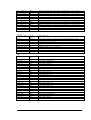
APPENDIX 1 – HERON SERIAL BUS COMMANDS ........................................... 59
MODULE ADDRESS ................................................................................................................................ 59
MODULE ENQUIRY ................................................................................................................................ 59
FPGA CONFIGURATION ........................................................................................................................ 59
4
HUNT ENGINEERING HERON-FPGA9 USER MANUAL
USER I/O ............................................................................................................................................... 60
APPENDIX 2 – FPGA PINOUT FOR DEVELOPMENT TOOLS ........................ 61
APPENDIX 3 – CREATING YOUR OWN DDR INTERFACE............................. 71
HOW MEMORY IS CONNECTED TO THE FPGA....................................................................................... 71
THE DDR CLOCK SCHEME.................................................................................................................... 74
CONTROLLING VREF GENERATION ........................................................................................................ 77
5
HUNT ENGINEERING HERON-FPGA9 USER MANUAL
Introduction
The HERON module is a module defined by HUNT ENGINEERING to address the
needs of our customers for real-time DSP systems. The HERON module is defined both
mechanically and electrically by a separate HERON module specification that is available
from the HUNT ENGINEERING CD, via the user manuals section from the CD
browser, or online from http://www.hunteng.co.uk and going to the application notes
section in the user area.
The HERON module specification also defines the features that a HERON module carrier
must provide. HERON stands for Hunt Engineering ResOurce Node, which tries to make
it clear that the module is not for a particular processor, or I/O task, but is intended to be a
module definition that allows “nodes” in a system to be interconnected and controlled
whatever their function. In this respect it is not like the TIM-40 specification which was
specific to the ’C4x DSP.
As the HERON-FPGA9 was developed, HUNT ENGINEERING have already developed
HERON modules carriers like the HEPC9, a range of HERON-FPGA modules that use
the Virtex-II FPGA and HERON processor modules (that carry various other members of
the TMS320C6000 family of DSP processors from TI). In addition to these modules, the
HERON specification is a super-set of the pre-existing HUNT ENGINEERING GDIO
module, so the GDIO modules from our ’C4x product range can also be used in HERON
systems.
The HERON module connects to the carrier board through several standard interfaces.
•
The first is a FIFO input interface, and a FIFO output interface. This is to be used for
the main inter-node communications. (It is usually also used for connection to the
HOST computer if any).
•
The second is the HERON Serial Bus, used for loading FPGAs and for non real time
configuration messages.
•
The last is the general control such as reset, power and General Purpose IO.
HUNT ENGINEERING defined the HERON modules in conjunction with HEART –
the Hunt Engineering Architecture using Ring Technology. This is a common architecture
that we have adopted for our HERON carriers that provides good real time features such
as low latency and high bandwidth, along with software reconfigurability of the
communication system, multicast, multiple board support etc., etc.
However, it is not a requirement of a HERON module carrier that it implements such
features. In fact our customers could develop their own module carrier and add our
HERON modules to it. Conversely our customers could develop application specific
HERON modules themselves and add them to our systems.
The HERON-FPGA9 is HERON module that can be used for hardware signal processing
or for flexible I/O.
The HERON-FPGA9 provides a Virtex-II Pro FPGA (Xilinx part number xc2vp7). For
more part information refer to the Xilinx web site at http://www.xilinx.com . This FPGA
provides user programmable logic along with an embedded Power PC core.
The HERON-FPGA9 connects all of the HERON module signals, except JTAG, to the
6
HUNT ENGINEERING HERON-FPGA9 USER MANUAL
FPGA, allowing flexible use of the module’s resources.
The HERON-FPGA9 provides a total of 256Mbytes of SDRAM, directly connected to the
pins of the Xilinx FPGA. This memory is organised as two separate 32 bit wide banks each
of which can be used as general-purpose memory by the FPGA, or connected to the Power
PC core. This allows the following combinations:
•
64 bit wide memory connected to the FPGA logic
•
64 bit wide memory connected to the Power PC core
•
32 bit wide memory connected to the FPGA logic and separate 32 bit wide memory
connected to the Power PC core
The HERON-FPGA9 provides a total of 16Mbytes of FLASH memory, directly connected
to the pins of the Xilinx FPGA. This memory is intended to hold boot code for the Power
PC in embedded applications.
The HERON-FPGA9 also provides 30 of the FPGA I/Os connected to connectors on the
module. This allows the FPGA to be configured for a variety of I/Os.
The HERON-FPGA9 also provides a USB “On The Go” (OTG) controller connected to
the FPGA allowing the module to act as a USB host or Peripheral. It allows “FullSpeed” (12Mbits/sec) and “Low-Speed” (1.5Mbits/sec), but not “Hi-Speed” (480
Mbits/sec) transfers.
The HERON-FPGA9 uses the HERON module’s serial bus to download configuration
bit-streams into the FPGA, allowing the user to configure it with standard functions
provided by HUNT ENGINEERING or functions that they have developed themselves
using the Xilinx development tools. It is also possible for the module to configure the
FPGA from a PROM. This is intended to simplify the deployment of systems after the
FPGA functions have been fully developed.
7
HUNT ENGINEERING HERON-FPGA9 USER MANUAL
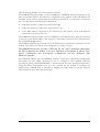
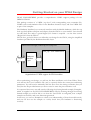
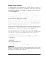
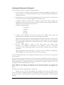
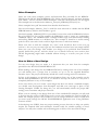
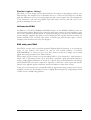
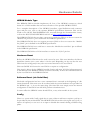
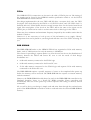
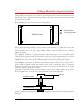
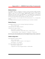
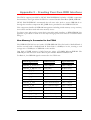
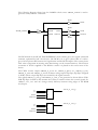
Physical Location of Items on the HERON-FPGA9
Power circuit
Power circuit
HERON connector
1.5V
Power good
LED
FLASH
Memory
256Mbytes of
DDR SDRAM
2.5V
Power good
LED
User
osc0
JTAG
USB
User
FPGA boot
from prom
jumper
Digital I/O B
Digital I/O A
HERON connector
Virtex II Pro
FPGA (XC2VP7)
PROM
USB chip
Power circuit
3.3V
Power good
LED
HERON connector
HERON connector
General
Purpose
LEDs
8
Control
FPGA “CNT
DONE” LED
User FPGA
“DONE” LED
HUNT ENGINEERING HERON-FPGA9 USER MANUAL
Getting Started
The HERON-FPGA9 is a module that plugs into a HERON module carrier.
The HERON-FPGA9 should be fitted to the carrier card along with any other modules
that your system has and their retaining nuts fitted (see a later section of this manual for
details).
The HERON-FPGA9, following reset, will enter a state where it can be interrogated and
programmed using the HERON module’s serial bus. It is addressed according to the
Carrier number and the slot number of the HERON slot that it is fitted to.
The FPGA configuration data will have been generated using the Xilinx development tools.
HUNT ENGINEERING provide examples for the HERON-FPGA modules in the
correct format for use with the Xilinx ISE software. HUNT ENGINEERING also
provides software for the Host PC that will allow the output files from the Foundation
software to be loaded onto a HERON-FPGA module. If you use the Power PC core in the
FPGA you will also need the Xilinx Embedded Developers Kit (EDK).
If you are using the module on an embedded module carrier where there is no connection
to a host machine, you can use a Xilinx Parallel 4 cable plugged into the JTAG connector
on the module, to download your FPGA design. This connection can also be used to debug
the FPGA design using the Xilinx Chipscope software, and to debug the Power PC code
using the GNU debugger supplied in the Xilinx EDK.
Follow the “Starting your FPGA development” tutorial from the HUNT ENGINEERING
CD, and then the general FPGA examples found in the same place on the CD.
It could be possible to use the HERON-FPGA9 as an I/O or memory module using one
of the example bit streams. In this case it is not necessary to be concerned how to program
the FPGA – simply load the example bit stream and use it.
Standard Intellectual Property (IP)
HUNT ENGINEERING provides examples for the HERON-FPGA9 that perform
different functions. It is possible to use these standard configurations directly if they fit your
needs.
It could be possible to request a new standard example from HUNT ENGINEERING,
which could avoid the need to purchase and learn how to use the FPGA development
tools. Depending on the complexity of your request HUNT ENGINEERING may choose
not to offer it, or to charge for it.
New IP for the HERON-FPGA9 will be posted on the HUNT ENGINEERING web site
in the user area whenever it becomes available. HERON-FPGA9 users can then take
advantage of that IP free of charge.
9
HUNT ENGINEERING HERON-FPGA9 USER MANUAL
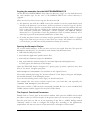
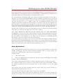
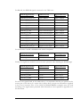
Module Features
This section describes the features of the HERON-FPGA9 and why they are provided.
DDR
SDRAM
FLASH
memory
DDR
SDRAM
LEDs
30 bits Digital I/O
Power
Supply Cct
USB
JTAG PROM
FPGA – XC2VP7
Clock
options
Configuration
control FPGA
HERON FIFO CONNECTIONS
HERON CONTROLS
HERON Serial Bus
User Programmable FPGA with Embedded Power PC
The Virtex-II Pro FPGA on the HERON-FPGA9 offers both user programmable
hardware in the form of Virtex-II like FPGA architecture, and a Power PC processor core
that is embedded in silicon. The HERON-FPGA9 allows the user to program the FPGA
logic and Power PC processor using the tools provided by Xilinx. The module design does
not place any restriction on how the FPGA program can be configured. There are many
examples and tutorials provided by Xilinx that help you to use the architecture (including
the embedded Power PC). HUNT ENGINEERING provides an application note separate
from this user manual that guides you through the use of the embedded Power PC in a
HERON system.
Serial Configuration of the User FPGA
The HERON-FPGA9 usually has the configuration of the user FPGA downloaded using
the HERON module’s serial configuration bus. This allows the use of “standard”
configurations as supplied on the HUNT ENGINEERING CD, or of user defined
configurations without the need to return the module to the factory.
It is imagined that as the “standard” set of functions grows, that they be made available to
users of HERON-FPGA modules via the HUNT ENGINEERING web site or CD update
requests. Also HUNT ENGINEERING will have the possibility to provide semi-custom
configurations for a charge via email.
USER FPGA boot ROM
As an alternative to the serial configuration download, it is possible to configure the FPGA
from a Flash based configuration PROM However, if a system is being deployed with a
10
HUNT ENGINEERING HERON-FPGA9 USER MANUAL
host machine such as a PC, it might be preferable to continue to use the serial configuration
method, as this will make in field upgrades and bug fixes simpler to deploy.
The PROM fitted to the FPGA9 is Flash based (XCF08P), and can be programmed (and
re-programmed) using a Xilinx JTAG cable 4. An option in the JTAG download software
can cause the FPGA to be configured on completion of the PROM being programmed.
11
HUNT ENGINEERING HERON-FPGA9 USER MANUAL
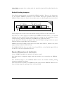
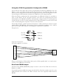
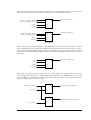
Clocking of the FPGA
The Xilinx FPGA used on the HERON-FPGA9 does not have a single clock input, but
rather it can use any one of its pins to provide a clock input. This means you can have many
sources of clocks, each of which can be used inside your FPGA design. You can even
divide these clocks using flip flops, or even multiply using digital clock manager (DCM)
components.
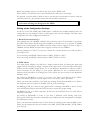
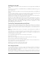
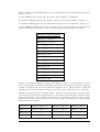
Clock Options
OSC3 (100Mhz)
User OSC0
SDRAM CLK IN (200Mhz)
Digital I/Os
UMI 0,1,2&3
buffer
buffer
Your FPGA design
Necessary clocks
Output FIFO clock
feedback
Input FIFO clock
feedback
SDRAM clock
The simplest way to manage your FPGA design is to use just one clock throughout your
design. However the FPGA must drive both of the HERON FIFO clocks, at a frequency
that is suitable for your module carrier (see the documentation for your module carrier for
details of its restrictions). The FPGA must also drive the SDRAM clock, at a frequency
suitable for the SDRAM (200MHz). The FPGA may also need to use clocks for the digital
I/Os. The frequency for these might be limited by the equipment that it is connected to, or
by the needs of your signal processing. The needs for these clocks can only be determined
by looking carefully at the needs of your system.
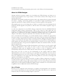
Clock Options
OSC3 (100Mhz)
User OSC0
SDRAM CLK IN (200Mhz)
Digital I/Os
UMI 0,1,2&3
buffer
buffer
Div2?
Logic
Necessary clocks
Output FIFO clock
feedback
Input FIFO clock
feedback
SDRAM clock
DCM
Example1 design
If these clocks cannot be the same, then the next best situation is to have one clock derived
from the other. In that way the relationship between the clock edges will be known.
The most difficult case for your FPGA design is to have many clocks from different
sources that are all used in the same design. Then you must carefully manage signals that
cross from one clock “domain” to another. This can be handled by FIFOS, or by multiple
registering to prevent metastability problems. Refer to texts on digital design to understand
these issues. Our standard examples actually use separate clock domains for the HERON
FIFOs and the DDR SDRAM. You can see in those standard designs that FIFOs have
12
HUNT ENGINEERING HERON-FPGA9 USER MANUAL
been used to pass data between those two clock domains.
The HERON-FPGA9 provides a highly flexible set of choices for the clocking of the
FPGA.
The HERON-FPGA9 has a socket for a 3.3V user oscillator.
Default shipping state is to have a 100MHz oscillator fitted to one of the surface mount
sites – driving 100MHz on UserOsc3. This is a standard commercial oscillator module, that
is +/-100ppm accuracy. If you require higher accuracy clocks then you should use one of
the other clock sources.
Also the Digital I/Os and UMI pins on the module connector could be used as a clock
input, if another module in the system is programmed to drive that clock onto the UMI
connection.
HERON FIFOS
The HERON module can access up to 6 input FIFOs and up to another 6 output FIFOs.
Each FIFO interface is the same as the others, using common clocks and data busses.
The input and output interfaces are separate though, allowing data to be read and written at
the same time by a module like the HERON-FPGA9.
While it is possible to read one FIFO and write another FIFO at the same time, the use of
shared pins means no more than one can be written or read at the same time (i.e. in the
same clock cycle).
For each interface (input or output) there is a FIFO clock that must be a constant
frequency, and running constantly. There may be some minimum and maximum frequency
requirements for a particular Module Carrier card that the designer of the FPGA contents
must be sure to comply with. This is because the FIFO clocks are generated by the FPGA,
probably based on one of the clock inputs to the part.
Each FIFO interface has a separate “enable” signal that is used to indicate which FIFO is
accessed using the clock edge.
Input FIFOs
The six input FIFOs use a common data bus that is driven onto the HERON module. It is
important to ensure that no more than one of the FIFOs are read at the same time, but
more importantly that no more than one has its output enable selected.
By properly asserting the “read enable” and “output enable” signals relative to the clock the
FPGA can access the FIFO of its choice at a rate up to one 32 bit word per clock cycle.
For the timing of those signals refer to the HERON module specification.
Each input FIFO interface provides Flags that indicate the state of the FIFO. An empty
flag shows that there is no data to be read, an almost empty flag shows that there are at least
4 words left. While the almost flag is not asserted accesses can be made on every clock, but
after it is asserted, it is better to make one access only, then check the empty flag on the
next clock, before deciding if another access is possible.
13
HUNT ENGINEERING HERON-FPGA9 USER MANUAL
Output FIFOs
The six output FIFOs use a common data bus that is driven by the HERON module. It is
important to ensure that no more than one of the FIFOs is written at the same time –
unless that is required by your system.
By properly asserting the “write enable” signals relative to the clock, the user FPGA can
access the FIFO of its choice at a rate up to one 32-bit word per clock cycle.
For the timing of those signals refer to the HERON module specification.
Each output FIFO interface provides Flags that indicate the state of the FIFO. A full flag
shows that there is no room left to write, an almost full flag shows that there are at least 4
words of space left. While the almost flag is not asserted accesses can be made on every
clock, but after it is asserted, it is better to make one access only, then check the full flag on
the next clock, before deciding if another access is possible.
FIFO clocks
The FIFO clocks are provided by the user FPGA, but are buffered externally using an
LVT245 buffer that is able to provide the drive current required on these signals. To enable
circuitry internal to the FPGA to be designed to use the actual clock that is applied to the
FIFO, the buffered FIFO clock signals are connected to the remaining GCLK inputs. This
allows DLLs to be used to provide a clock internal to the FPGA that has the same phase as
that applied to the FIFOs on the carrier board.
DDR SDRAM
The HERON-FPGA9 provides two completely independent 128Mbyte banks of 200MHz
Double Data Rate (DDR) SDRAM directly connected to the I/O pins of the Virtex-II Pro
FPGA. Each bank of the DDR SDRAM is organised as a 32-bit wide memory bank of 32M
locations.
In order to use the DDR SDRAM correctly, an appropriate DDR SDRAM controller
function is required inside the FPGA. This controller must correctly initialise the DDR
SDRAM, and provide a constant refresh mechanism.
An appropriate DDR SDRAM controller is provided in the Hardware Interface Layer
VHDL support from HUNT ENGINEERING.
One bank of DDR SDRAM is built from two pieces of 512Mbit Micron SDRAM. The
SDRAM used is Micron part number MT46V32M16TG-5B.
FLASH Memory
The HERON-FPGA9 provides a 16Mbyte FLASH PROM directly connected to the I/O
pins of the Virtex-II Pro FPGA. It is intended to be used to store boot code for the Power
PC core, but the user is free to connect it and use it however they want. It is organised as a
byte wide memory bank of 16M locations. It is an Intel Flash memory part number
28F128J3.
In order to use the FLASH memory correctly, an appropriate FLASH memory controller
function is required inside the FPGA. The FLASH then requires some protocols to be
followed in order to unlock the writing of the part.
14
HUNT ENGINEERING HERON-FPGA9 USER MANUAL
If the FLASH memory is used as intended (connected to the Power PC core) Xilinx
provide a Core that will directly connect to and control this FLASH memory. Xilinx also
provide a large amount of driver software to take account of the protocols.
Users can develop their own uses of this FLASH memory, in which case they will need to
refer to the Intel documentation for this memory.
Digital I/O
The HERON-FPGA9 connects 30 of the FPGAs I/O pins to connectors. This allows
them to be configured as digital Inputs and Outputs as chosen by the user’s FPGA
program.
For the HERON-FPGA9, Vcco is always selectable between 3.3V and 2.5V. Therefore, all
FPGA I/O pins used with the Digital I/O connectors can use I/O formats with either of
those Vcco settings.
Module and Carrier ID
The HERON specification assigns pins on the HERON module that give a HERON
module access to the carrier ID of the carrier that it is plugged into, and a unique HERON
slot identifier.
These IDs are used by the configuration FPGA so that the module is addressed on
HERON Serial Bus (HSB) using this information. These signals are also connected to the
User FPGA so a user program can use them if required.
General Purpose LEDs
There are some LEDs on the HERON-FPGA9 that are connected to some of the FPGA
I/O pins. There are five such LEDs, which can be used by the FPGA program to indicate
various states of operation.
Done LEDs
There are two Done LEDs, labelled “DONE” and “CNT DONE”. They are illuminated if
the relevant FPGA is not configured.
LED “DONE” is connected to the user Virtex-II Pro FPGA.
LED “CNT DONE” is connected to the Control FPGA.
This means that the “CNT DONE” should flash at power on, and then go out showing
that the control FPGA is ready to accept a configuration stream for the User FPGA.
After downloading a bitstream to the user User FPGA LED “DONE” should also go out.
USB
There is a connector on the HERON-FPGA9 that provides the opportunity to connect to
USB. This is connected through the Cypress CY7C67300 USB OTG controller. At the time
of release of the module this interface has not been tested by HUNT ENGINEERING so
15
HUNT ENGINEERING HERON-FPGA9 USER MANUAL
no support can be offered. In due time this support will be added to the Hardware Interface
Layer.
The controller chip requires software to be loaded onto it in order to correctly function.
There is a Serial PROM connected to the FPGA that is intended to be used for storing the
boot code for this device. The Serial PROM is an ST M25P20 2Mbit serial FLASH PROM.
16
HUNT ENGINEERING HERON-FPGA9 USER MANUAL
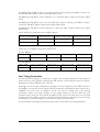
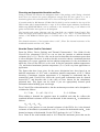
Getting Started on your FPGA Design
HUNT ENGINEERING provide a comprehensive VHDL support package for the
HERON-FPGA9.
This package consists of a VHDL “top level”, with corresponding user constraints file,
VHDL sources and simulation files for the Hardware Interface Layer, and User VHDL files
as part of the examples.
The Hardware Interface Layer correctly interfaces with the Module hardware, while the top
level (top.vhd) defines all inputs and outputs from the FPGA on your module. Users should
not edit these files unless a special digital I/O format is required – see the later section
“Digital I/O from the FPGA”.
The file user_ap.vhd is where you will make your design for the FPGA, using the simplified
interfaces provided by the Hardware Interface Layer.
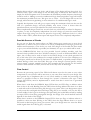
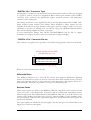
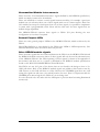
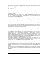
Entire FPGA design (VHDL top level) top.vhd
User_Ap – user VHDL level
I/O pins
Hardware
Interface
Layer
Organisation of VHDL support for FPGA modules
After synthesising your design, you will use the Place and Route tools from Xilinx. These
tools will use the User Constraints File (.ucf) to correctly define the correct pins and timing
parameters. You will need to minimally edit this file to have the timing constraints that you
need, but the file provided means you do not need to enter the pin constraints at all.
It is expected that every user will start by following the Getting Started example, Example1,
which is supplied on the HUNT ENGINEERING CD. By working through the Getting
Started example you will be able to see how the User FPGA is configured, how a simple
example can be built, and a new bitstream generated.
In this way, you can use Example1 to check your understanding of how the module works,
and you can also use the example as a sanity check that your hardware is functioning
correctly.
17
HUNT ENGINEERING HERON-FPGA9 USER MANUAL
Working through Example 1
All HERON modules that have FPGAs have an “Example1” provided for them. It is a
simple example that connects data from the input FIFO interface to the output FIFO
interface, and also exercises the HSB interface.
This example is fully described in the “Starting your FPGA development” tutorial on the
HUNT ENGINEERING CD.
The tutorial works through running the example and then modifying and re-building it. The
tutorial assumes that you are using the latest version of the ISE Foundation tool-set from
Xilinx. If you are using a different version of ISE Foundation, you will simply need to
convert the project as described in the application note provided by HUNT
ENGINEERING titled ‘Using Different Versions of ISE’. There is also an application note
on the HUNT ENGINEERING CD that describes using design flows that are different
from ISE, titled ‘Using VHDL tools other than ISE’.
The example is quite simple but demonstrates the use of the interfaces found in the
Hardware Interface Layer supplied with the module. The example is supplied in two ways.
Firstly, there is a ready-to-load bitstream, supplied in the Hunt Compressed Bitstream file
format, or ‘.hcb’ format. This is the file format used by the HUNT ENGINEERING
configuration tool. Secondly, there is an example1 project supplied for ISE, enabling the
design to be rebuilt and a new bitstream downloaded.
The bitstream file is provided to allow you to load the example1 onto the hardware without
having to re-build it. This is a useful confidence check to see if any problems you are
experiencing are due to changes you have made, or the way you have built the design. If the
bitstream from the CD fails to behave then the problem is more fundamental.
To make things easier, we have created the proper ISE project files for the examples.
Using these projects will allow you to run the complete design flow, from RTL-VHDL
source files to the proper bitstream, ready to download on your Heron FPGA board.
No special skills are required to do this.
However, if you want to write your own code and start designing your own application, you
must make sure that you have acquired the proper level of expertise in:
* VHDL language
* Digital Design
* Xilinx FPGAs
* ISE environment and design flow
Proper training courses exist which can help you acquire quickly the required skills and
techniques. Search locally for courses in your local language.
Preparing ISE
Before beginning work with Example1 you will need to make sure ISE is properly installed.
In addition, you should ensure that you have downloaded the latest service pack from the
Xilinx website for the version of ISE you are using.
18
HUNT ENGINEERING HERON-FPGA9 USER MANUAL
Copying the examples from the HUNT ENGINEERING CD
On the HUNT ENGINEERING CD, under the directory “fpga” you can find directories
for each module type. In the case of the HERON-FPGA9 the correct directory is
“fpga9v1”.
There are two ways that you can copy the files from the CD.
1) The directory tree with the VHDL sources, bit-streams etc can be copied directly from
the CD to the directory of your choice. In this case there is no need to copy the .zip file,
but the files will be copied to your hard drive with the same read only attribute that they
have on the CD. In this case all files in the example directories need to be changed to
have read/write permissions (‘Example1’, camera examples and SDRAM example
directories). It is a good idea to leave the permissions of the ‘Common’ directory set to
read only to prevent the accidental modification of these files.
2) To make the process more convenient we have provided the zip file, which is a zipped
image of the same tree you can see on the CD. If you “unzip” this archive to a directory
of your choice, you will have the file permissions already set correctly.
Opening the Example1 Project
Let us start with Example1. In the tree that you have just copied from the CD, open the
Example1 sub-directory. You should see some further sub-directories there:
* ISE holds the ISE project files.
* Src holds the application-specific Source files.
* Sim holds the simulation scripts for ModelSim.
* Leo_Syn holds the synthesis scripts for Leonardo Spectrum and Synplify users.
You may ignore this directory in this chapter.
Open the Xilinx ISE Project Navigator. If a project pops up (from a previous run), then
close it. Use File Æ Open project.
Select Example1\ISE\XXXXX.ise and click on the "Open" button.
After some internal processing, the "Sources window" of the Project Navigator will display
the internal hierarchy of the Example1 project.
If you are encountering errors at this stage, you should verify that:
The example files have been correctly copied onto your hard disk, and especially the
\Common and Example1\Src directories.
The correct version of ISE has been successfully installed. Be sure to have installed XST
VHDL synthesis and the support for the Virtex-II Pro family.
The Project's Functional Parameters
Double click on "user_ap1" in the Sources window. This opens the VHDL colour-coded
text editor so that you can see the part of the project where you can enter your own design.
The first code that you will see at the beginning of this file is a VHDL Package named
"config" which is used to configure the design files according to the application's
requirements. See the next section of this manual for a description of these items.
19
HUNT ENGINEERING HERON-FPGA9 USER MANUAL
Below the package section, you will see the User_Ap1's VHDL code.
This is where you will insert your own code when you make your own design.
We provide a system which is built in such a way that the user should not need to edit any
other file than User_Ap (and the entities that this module instantiates).
In particular, the user should NOT modify the HE_* files,
even when creating new designs for the FPGA.
Setting up the Configuration Package
At the top of the file USER_APx.VHD (where x indicates the example number) there are
settings that you can change to affect your design (in this case the example). The idea is that
settings that are often changed are found here.
1. Divide External Clock by 2
The example uses the 100MHz oscillator that is fitted to Osc3 of the module. It generates
the FIFO clock either directly from this 100MHz, or divides it by 2 to generate a 50MHz
FIFO clock. Unfortunately the HEPC8 module carrier cannot support a clock as high as
100MHz, and the HEPC9 carrier cannot support a clock as low as 50MHz.
Set this parameter to "True" if you want to divide the external clock by two and use this as
your main Clock.
If you are using an HEPC8 carrier board, set DIV2_FCLK to "True".
If you are using an HEPC9 carrier board, set DIV2_FCLK to "False".
2. FIFO Clocks
You must decide whether you will have a single common clock for driving the input and
output FIFOs. Normally a design is simpler if the same clock is used for input and output
FIFOs, but the module design allows you to use different frequencies or phases if that is
more convenient for the design of your system. Whether you use a common clock or
separate clocks will affect your design, but it also affects the use of clocks in the Hardware
Interface Layer.
Set FCLK_G_DOMAIN to True if you have the same clock driving both FIFOs.
This is the default option for the Examples. If you are unsure, select this choice.
Then, you must know whether your clocks are running slower than 60 MHz or not. This is
the frequency that you connect to the SRC_FCLK_G in your design.
Set HIGH_FCLK_G to True if your global clock is running at 60 MHz or above. In this
case an HF DLL will be used in the FIFO clocks to ensure the proper timing.
Set HIGH_FCLK_G to False otherwise. In this case the HF DLL does not work, and an
LF DLL is necessary.
Set FCLK_G_DOMAIN to False is you have a different clock driving each Fifo.
This option should be reserved to advanced users familiar with the management of multiple
clock domains systems.
Then, you must know whether each of your clocks are running slower than 60 MHz or not.
These are the frequencies that you connect to the SRC_FCLK_RD and SRC_FCLK_WR in
your user_ap.
20
HUNT ENGINEERING HERON-FPGA9 USER MANUAL
Set HIGH_FCLK_RD to True if your Input Fifo clock is running at 60 MHz or above, so
that the HF DLL will be used for the input FIFO clock.
Set HIGH_FCLK_RD to False otherwise, so a LF DLL will be used for the input FIFO
clock.
Set HIGH_FCLK_WR to True if your Output Fifo clock is running at 60 MHz or above,
so that the HF DLL will be used for the output FIFO clock.
Set HIGH_FCLK_WR to False otherwise, so that a LF DLL will be used for the output
FIFO clock.
The Table below summarises the available choices:
FCLK_G_DOMAIN
HIGH_FCLK_G
HIGH_FCLK_RD
HIGH_FCLK_WR
True
True / False
n.a.
n.a.
False
n.a.
True / False
True / False
In the case of example1, the correct choices are:
For the HEPC8
DIV2_FCLK
FCLK_G_DOMAIN
HIGH_FCLK_G
HIGH_FCLK_RD
HIGH_FCLK_WR
True
True
False
n.a.
n.a.
DIV2_FCLK
FCLK_G_DOMAIN
HIGH_FCLK_G
HIGH_FCLK_RD
HIGH_FCLK_WR
False
True
True
n.a.
n.a.
For the HEPC9
User Timing Constraints
As with all FPGA designs it is necessary to apply some timing constraints to the design to
ensure that the tools generate a design that will operate at the frequency that you require.
Example1 has these defined in the ‘.ucf’ file.
Although you can use the configuration package to set the frequency of the FIFO clocks to
be 50MHz, you can still use the stricter timing constraints needed when those clocks run at
100MHz. So in the case of example1 you do not need to change any of the timing
constraints. When you make changes to the design however you may find that you
introduce more clock nets that need to be added to the ucf file. In some cases you may find
that the tools are unable to achieve your desired clock frequency and then (if you are using
an HEPC8) you should change the constraints to reflect you true needs.
For more details on Timing Constraints please refer to the Xilinx tools documentation.
21
HUNT ENGINEERING HERON-FPGA9 USER MANUAL
Creating the Bitstream for Example1
Once the project has been opened as described above:
1. In the "Sources in project" window (Project Navigator), highlight (single-click on)
the entity ‘top’ ("..\..\Common\top.vhd"). This is extremely important! Otherwise,
nothing will work!
2. Double-click on the "Generate Programming File" item located in the "Processes
for Current Source". This will trigger the following activity:
Complete synthesis, using all of the project's source files. Since warnings are
generated at this stage, you should see a yellow exclamation mark appear besides the
"Synthesize" item in the Processes window.
Complete Implementation:
Translation
Mapping
Placing
Routing
3. Creation of the bitstream. Note that this stage runs a DRC check, which can
potentially detect anomalies created by the Place and route phase.
When the processing ends, the proper bitstream file, with extension ".rbt" can be
found in the project directory. This file MUST be called top.rbt. If it is not then you
have synthesised a small part of your design because you did not properly highlight
top.vhd in step1.
4. In the "Pad Report" verify a few pins from the busses, like:
LED(0) = G17, LED(1) = H16, LED(2) = F17, LED(3) = F16, etc... To do this
you need to open “implement design” in the processes window, then open “Place
and Route”.
Then double click on the pad report to open it. If you see different assignments,
STOP HERE, and verify the UCF file selected for the project.
You can download this file on your FPGA board and see how it works. See a later section
of this manual.
Note that the user_ap level includes a very large counter that divides the main system clock
and drives the LED #4. It is then obvious to see if the part has been properly programmed
and downloaded: the LED should flash. The hardware will probably require a reset after
configuration before the LED starts to flash.
If the LED does not flash, we recommend that you shut down the PC or reprogram the
device using a "safe" bitstream. Otherwise, some electrical conflicts may happen (see
below).
Possible causes for the device failure to operate are:
1.
Wrong (or no) UCF file. This happens (for example) if you select the XST-version
of the UCF with a Leonardo Spectrum (or Synplify) synthesis. The pin assignment for all
the vectors (busses) will be ignored, and these pins will be distributed in a quasi-random
fashion!
22
HUNT ENGINEERING HERON-FPGA9 USER MANUAL
2.
Wrong parameters in the CONFIG package.
3.
Design Error.
If nothing seems obvious, rerun the confidence tests, then return to the original example 1.
Simulating the Complete Design
To generate the bitstream as above, you did not need to do any simulation. However, if you
start modifying the provided examples and add your own code, verification can soon
became an important issue.
If you need to simulate your design, you will need to install a VHDL simulator such as
ModelSim (available in Xilinx Edition, Personal Edition, or Special Edition).
The example projects provided on the HUNT ENGINEERING CD include simulation
files that provide a starting point for simulating your own design. If you wish to work
through the simulation examples provide, please read the document ‘Simulating HERON
FPGA Designs’.
23
HUNT ENGINEERING HERON-FPGA9 USER MANUAL
Making your own FPGA Design
The actual contents of the User FPGA on the HERON-FPGA9 are generated by the user.
While making this development requires some knowledge of Digital Design techniques, it is
made quite simple by the development environment that you use.
We recommend the Foundation ISE series software available from Xilinx, because that is
what we use at HUNT ENGINEERING, and any examples and libraries we provide are
tested in that environment. However there are other tools available from third parties that
can also be used. The use of VHDL sources for our Hardware Interface Layer and
examples means that virtually any FPGA design tool could be used. Any development tool
will eventually use the Xilinx Place and Route tool, where the user constraints file that we
supply will ensure that the design is correctly routed for the module. There are application
notes on the HUNT ENGINEERING CD that describe how other tools might be used.
The best way to learn how to use your development tools is to follow any tutorials provided
with them, or to take up a training course run by their vendors.
ALL NEW PROJECTS SHOULD START FROM ONE OF THE PROVIDED
EXAMPLES – that way all of the correct settings are made, and files included. Your design
should take place entirely within the User-Ap level, except in the case of needing to change
the I/O formats of the Digital I/Os in which case it is necessary to minimally edit the
top.vhd file – see a later section in this manual for details.
It is assumed that you are able to use your tools and follow the simplest of Digital Design
techniques. HUNT ENGINEERING cannot support you in these things, but are happy to
field questions specific to the hardware such as “how could I trigger my A/D from a DSP
timer?” or “How can I use the FIFO interface component to do….?”.
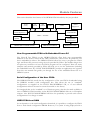
User_Ap Interface
This section describes the Interface between the User_Ap central module (or entity using
VHDL terminology) and the external Interface hardware. This is the part where you
connect your FPGA design to the resources of the module.
In other words:
1.
The Clocks system
2.
How your application can communicate with the external world: Digital I/Os, HSB
interface, FIFOs and SDRAM.
You need to understand this interface in order to properly connect your processing logic.
The complete FPGA project consists of a Top level in which many sub-modules (entities)
are placed (instantiated) and interconnected. One of these modules is User_AP: your
module.
The top-level and the other modules make the system work, but you do not have to
understand nor modify them in any way.
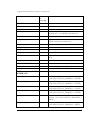
Let us see all of the Inputs/Outputs (Ports) of your User_Ap module:
Note that the names used for these ports are effectively “reserved” even if the user does not
connect to that signal. This means the user must be careful not to re-use the same name for
24
HUNT ENGINEERING HERON-FPGA9 USER MANUAL
a signal that should not connect to these ports.
Port
Direction
in
User_Ap
Description
RESET
In
Asynchronous module reset (active high)
CONFIG
In
System config signal (active low)
ADDR_FLAGSEL
In
Module input to select the mode of some
module pins – see HERON specification
BOOTEN
Out
Module output not normally used
UMI_EN[0:3]
Out
Uncommitted Module Interconnect enables,
FPGA output driven when low
UMI_IN[0:3]
In
Uncommitted Module Interconnects in
UMI_OUT[0:3]
Out
Uncommitted Module Interconnects out
MID[0:3]
In
Module ID of this module slot
CID[0:3]
In
Carrier ID of this carrier
UDPRES
Out
Optional reset to system. Drive to ‘1’ if not
used.
LED[0:4]
Out
5 x LEDs, can be used for any purpose
OSC0
In
External Clock from OSC0 oscillator
OSC3
In
External Clock from OSC3 oscillator
FCLK_RD
In
Read FIFO Clock to be used in this module
(only when FCLK_G_DOMAIN = FALSE)
SRC_FCLK_RD
Out
Input FIFO Clock source for the top level
(only when FCLK_G_DOMAIN = FALSE)
FCLK_WR
In
Output FIFO Clock to be used in this module
(only when FCLK_G_DOMAIN = FALSE)
SRC_FCLK_WR
Out
Output FIFO clock source for the top level
(only when FCLK_G_DOMAIN = FALSE)
FCLK_G
In
Common FIFO clock to be used in this
module (only when FCLK_G_DOMAIN =
TRUE)
SRC_FCLK_G
Out
Common FIFO clock source for the top level
(only when FCLK_G_DOMAIN = TRUE)
GENERAL
CLOCK SOURCES
FIFO
INTERFACE
CLOCK
25
HUNT ENGINEERING HERON-FPGA9 USER MANUAL
INPUT FIFOs
INFIFO_READ_REQ[5:0]
Out
Input FIFO Read Request
INFIFO_DVALID[5:0]
In
Input FIFO Data Valid
INFIFO_SINGLE[5:0]
In
Input FIFO Single Word Available
INFIFO_BURST[5:0]
In
Input FIFO Burst Possible
INFIFO0_D [31:0]
In
Input FIFO 0 Data
INFIFO1_D [31:0]
In
Input FIFO 1 Data
INFIFO2_D [31:0]
In
Input FIFO 2 Data
INFIFO3_D [31:0]
In
Input FIFO 3 Data
INFIFO4_D [31:0]
In
Input FIFO 4 Data
INFIFO5_D [31:0]
In
Input FIFO 5 Data
OUTFIFO_READY[5:0]
In
Output FIFO Ready for Data
OUTFIFO_WRITE[5:0]
Out
Output FIFO Write Control
OUTFIFO_D [31:0]
Out
Data written into Output FIFO
MSG_CLK
Out
Clock to HE-USER interface logic.
MSG _DIN [7:0]
In
Data received from HSB
MSG _ADDR [7:0]
In
"address" received from the HSB
MSG _WEN
In
Write access from the HSB
MSG _REN
In
Read access from the HSB
MSG _DONE
In
Message was successfully transmitted (used
when initiating HSB messages)
MSG _COUNT
In
Counter enable when initiating HSB messages
MSG _CLEAR
In
Asynchronous clear for address counter when
initiating HSB messages
MSG _READY
Out
to acknowledge an access from the HSB
MSG _SEND
Out
Message send command (used when initiating
HSB messages)
MSG _CE
Out
to control speed operation
MSG _DOUT [7:0]
Out
Data to be sent to HSB
MSG _SEND_ID
Out
Indicates when a byte should be replaced by
Own ID (used when initiating HSB messages)
MSG _LAST_BYTE
Out
To indicate when the last byte to be sent is
presented when initiating HSB messages
OUTPUT FIFOs
HE_USER I/F
26
HUNT ENGINEERING HERON-FPGA9 USER MANUAL
DIGITAL I/O
CONN_A_EN[14:0]
Out
Digital I/O enables for connector A, FPGA
output pin driven when low
CONN_A_IN[14:0]
In
Digital I/O in for connector A
CONN_A_OUT[14:0]
Out
Digital I/O out for connector A
CONN_B_EN[14:0]
Out
Digital I/O enables for connector B, FPGA
output pin driven when low
CONN_B_IN[14:0]
In
Digital I/O in for connector B
CONN_B_OUT[14:0]
Out
Digital I/O out for connector B
FLASH_ADDR[23:0]
Out
FLASH Address
FLASH_IN[7:0]
In
FLASH Data In
FLASH_OUT[7:0]
Out
FLASH Data Out
FLASH_EN[7:0]
Out
FLASH Data Enable, FPGA output pin
driven with FLASH Data Out when low
FLASH_CE
Out
FLASH Chip Enable
FLASH_WE
Out
FLASH Write Enable
FLASH_OE
Out
FLASH Output Enable
FLASH_RP
Out
FLASH Reset / Power Down
FLASH_VPEN
Out
FLASH Program Enable
FLASH_STS
In
FLASH Status
DDR_A_USER_CLK
Out
DDR Port A User Clock Source
DDR_A_USER_RST
Out
DDR Port A Data Count User Reset
DDR_A_DATA_COUNT
[31:0]
In
DDR Port A Data Count
DDR_A_WR_DATA[71:0]
Out
DDR Port A Write Data
DDR_A_WR_ADDR[24:0]
Out
DDR Port A Write Address
DDR_A_WR_ADDR_
WEN
Out
DDR Port A Write Address Enable
DDR_A_WR_ADDR_FF
In
DDR Port A Write Address Full
DDR_A_WR_ADDR_AF
In
DDR Port A Write Address Almost Full
DDR_A_WR_RISE_WEN
Out
DDR Port A Write Rising Data Enable
DDR_A_WR_RISE_FF
In
DDR Port A Write Rising Data Full
DDR_A_WR_RISE_AF
In
DDR Port A Write Rising Data Almost Full
FLASH I/F
DDR SDRAM I/F
27
HUNT ENGINEERING HERON-FPGA9 USER MANUAL
DDR_A_WR_FALL_WEN
Out
DDR Port A Write Falling Data Enable
DDR_A_WR_FALL_FF
In
DDR Port A Write Falling Data Full
DDR_A_WR_FALL_AF
In
DDR Port A Write Falling Data Almost Full
DDR_A_WR_DM_WEN
Out
DDR Port A Write Data Mask Enable
DDR_A_WR_DM_FF
In
DDR Port A Write Data Mask Full
DDR_A_WR_DM_AF
In
DDR Port A Write Data Mask Almost Full
DDR_A_RD_DATA[63:0]
In
DDR Port A Read Data
DDR_A_RD_ADDR[24:0]
Out
DDR Port A Read Address
DDR_A_RD_ADDR_WEN Out
DDR Port A Read Address Enable
DDR_A_RD_ADDR_FF
In
DDR Port A Read Address Full
DDR_A_RD_ADDR_AF
In
DDR Port A Read Address Almost Full
DDR_A_RD_RISE_REN
Out
DDR Port A Read Rising Data Enable
DDR_A_RD_RISE_EF
In
DDR Port A Read Rising Data Empty
DDR_A_RD_RISE_AE
In
DDR Port A Read Rising Data Almost Empty
DDR_A_RD_FALL_REN
Out
DDR Port A Read Falling Data Enable
DDR_A_RD_FALL_EF
In
DDR Port A Read Falling Data Empty
DDR_A_RD_FALL_AE
In
DDR Port A Read Falling Almost Empty
DDR_B_USER_CLK
Out
DDR Port B User Clock Source
DDR_B_USER_RST
Out
DDR Port B Data Count User Reset
DDR_B_DATA_COUNT
[31:0]
In
DDR Port B Data Count
DDR_B_WR_DATA[71:0]
Out
DDR Port B Write Data
DDR_B_WR_ADDR[24:0]
Out
DDR Port B Write Address
DDR_B_WR_ADDR_
WEN
Out
DDR Port B Write Address Enable
DDR_B_WR_ADDR_FF
In
DDR Port B Write Address Full
DDR_B_WR_ADDR_AF
In
DDR Port B Write Address Almost Full
DDR_B_WR_RISE_WEN
Out
DDR Port B Write Rising Data Enable
DDR_B_WR_RISE_FF
In
DDR Port B Write Rising Data Full
DDR_B_WR_RISE_AF
In
DDR Port B Write Rising Data Almost Full
DDR_B_WR_FALL_WEN
Out
DDR Port B Write Falling Data Enable
DDR_B_WR_FALL_FF
In
DDR Port B Write Falling Data Full
DDR_B_WR_FALL_AF
In
DDR Port B Write Falling Data Almost Full
DDR_B_WR_DM_WEN
Out
DDR Port B Write Data Mask Enable
28
HUNT ENGINEERING HERON-FPGA9 USER MANUAL
DDR_B_WR_DM_FF
In
DDR Port B Write Data Mask Full
DDR_B_WR_DM_AF
In
DDR Port B Write Data Mask Almost Full
DDR_B_RD_DATA[63:0]
In
DDR Port B Read Data
DDR_B_RD_ADDR[24:0]
Out
DDR Port B Read Address
DDR_B_RD_ADDR_WEN
Out
DDR Port B Read Address Enable
DDR_B_RD_ADDR_FF
In
DDR Port B Read Address Full
DDR_B_RD_ADDR_AF
In
DDR Port B Read Address Almost Full
DDR_B_RD_RISE_REN
Out
DDR Port B Read Rising Data Enable
DDR_B_RD_RISE_EF
In
DDR Port B Read Rising Data Empty
DDR_B_RD_RISE_AE
In
DDR Port B Read Rising Data Almost Empty
DDR_B_RD_FALL_REN
Out
DDR Port B Read Falling Data Enable
DDR_B_RD_FALL_EF
In
DDR Port B Read Falling Data Empty
DDR_B_RD_FALL_AE
In
DDR Port B Read Falling Almost Empty
Hardware Interface Layer
All of the signals listed above are connected between the ‘User_Ap’ interface and the pins
of the FPGA via the ‘Hardware Interface Layer’. The Hardware Interface Layer includes
logic that correctly interfaces many different functional parts of the FPGA, from HERONFIFO interfaces, DDR SDRAM interface, to clock inputs and outputs, to digital I/O and
serial I/O.
For a complete description of the Hardware Interface Layer (HIL), please read the
document ‘Using the Hardware Interface Layer in your FPGA Design’.
Important!
The FPGA sets any I/O pins of the device that are not listed in the design to have a 50150K pull down. Most of the HERON module signals are pulled to their inactive state by
10K resistors so this 50K will have no effect. However the UDPRES signal does not, and
setting this signal low will cause your whole board to be reset. Thus it is important that the
UDPRES pin is driven high by the FPGA if it is not being used.
It is also advised to do the same with the LED pins to prevent them becoming illuminated
erroneously.
29
HUNT ENGINEERING HERON-FPGA9 USER MANUAL
Other Examples
There are some other examples (source and bitstream files) provided for the HERONFPGA9 on the HUNT ENGINEERING CD. Follow “Getting Started” and then “Starting
with FPGA”. Choose “General FPGA Examples” and click on the directory for the fpga9.
The examples are in the directories Memory_Test(ex2), SDRAM_FIFO(ex3) etc.
These examples have ‘pdf’ documents that describe their function.
The second example, ‘Memory_Test’ is useful for users who wish to validate that the DDR
SDRAM memory fitted to their module is good.
The third example, ‘SDRAM_FIFO’ is provided for users who need the SDRAM to behave
like a big FIFO. In fact, in this example the SDRAM is used to create two independent
128Mbyte FIFOs. The ‘SDRAM FIFO’ example includes logic that demonstrates reading
and writing DDR memory at 1.6Gbytes/sec. This example is therefore a useful starting
point for those users who need to achieve high data rates to and from memory.
Please note that as with the examples any “user” work should be done in the user_ap
section i.e. do not put your own logic into the hardware interface layer, but simply include
them into your own design. This enables your design to be protected from hardware
specific details like pin-out, and also allows you to benefit from any new versions that
HUNT Engineering might make available without having to re-work your part of the
design.
How to Make a New Design
For any new design that you make, it is important that you start from the examples
provided on the HUNT ENGINEERING CD.
When making a new design for the HERON-FPGA9 by starting from one of the examples
you will already have a project that is correctly set up to use the supplied Hardware
Interface Layer. The project will already include the correct settings and user constraints.
In fact, in all situations you should start development from one of the examples on the
HUNT ENGINEERING CD, even if you intend to develop the FPGA in a way that is
completely different to any of the examples.
In the case where you are to make a new design that does not match a standard example,
you should start development from Example1 and add your own logic in place of the
existing Example1 VHDL. By doing this, you will automatically inherit the proper ISE
settings, user constraints and project structure.
When your are creating a new design from one of the standard CD examples you will need
to be sure that the version of ISE design tools you are using matches the version of ISE for
which the example projects were created. If you are using a different version of ISE then
you must work through the HUNT ENGINEERING application note ‘Using Different
Versions of ISE’.
In developing new VHDL, there are proper training courses that exist to help you quickly
acquire the required skills and techniques. Search locally for suitable training on these
subjects. You may also consider sub-contracting part or whole of the new FPGA design.
30
HUNT ENGINEERING HERON-FPGA9 USER MANUAL
Inserting your own Logic
When making a new design, you will create and insert your own logic inside the USER_AP
module.
From here you can interface to the HERON FIFOs, the SDRAM, the HSB and the general
purpose digital I/Os.
When these interfaces are simple, you may code the proper logic directly in the USER_AP
module.
For more complex interfaces, you may code separate entities in separate source files, and
instantiate these entities within USER_AP, as was done in the Examples.
Important: the first thing to edit in the user_ap.vhd file is the package section where generic
parameters are set to match your configuration and your design.
Important: The HE_USER interface cannot be left entirely unconnected. If you have a
design that does not use the features of this interface, you must be certain to connect the
following. The Clock of the HE_USER must be running. The inputs MSG_SEND,
MSG_SEND_ID, MSG_LAST_BYTE and MSG_CS must be connected to 0. The
MSG_READY must be connected to ‘1’.
Top-level Fine Tuning (using other special IO pins)
The top level defines all of the I/O pins from the FPGA. Some of them are not used in the
examples, but have buffers instantiated in the top.vhd. Some of those pins can have
alternative signal formats that require a different Xilinx primitive to be instantiated for the
buffers.
Refer to the hardware details section of this manual to learn which pins are suitable for
which use.
If the buffers that are already instantiated in top.vhd (usually LVTTL) are suitable for your
needs then there is no need to modify top.vhd, you can simply use the signals that are
connected as ports to the user_ap file.
If you need different buffer types then it is necessary to edit top.vhd.
The method to do that is:
Make a copy of the original TOP.vhd file (from /Common) and work on this copy.
Each I/O pin has a buffer type instantiated in top.vhd.
Edit the instantiation to use the proper Xilinx Buffer primitive. You may sometimes have to
insert attributes in the UCF file to qualify the IO.
Modify the User_Ap entity to make these signals visible.
Add the signals in the User_Ap instantiation port map.
User Timing Constraints
As with all FPGA designs it is necessary to apply some timing constraints to the design to
ensure that the tools generate a design that will operate at the frequency that you require.
These will be defined in the .ucf file.
The .ucf file provided as a template has some timing constraints already, but when you
make changes to the design you may find that you introduce more clock nets that need to
31
HUNT ENGINEERING HERON-FPGA9 USER MANUAL
be added to the ucf file.
For more details on Timing Constraints please refer to the Xilinx tools documentation.
Hints for FPGA Designs
Having said that we cannot support you in making your FPGA design, we always try to
make your development easy to get started, so this section outlines some things that you
need to think about.
The FPGAs are basically synchronous devices, that is they register data as it passes through
the device – making a processing pipeline. It is possible to apply asynchronous logic to
signals but the FPGA concept assumes that logic is between registers in the pipeline.
This pipeline gives rise to two things that you need to consider. One is the maximum clock
frequency that that pipeline can operate at, and the other is the number of pipeline stages in
the design.
As with any component in your FPGA design, components from the HERON-FPGA9
component library operate synchronously. That is, any control or data signal that you
connect to the library component must be generated from logic that uses the same clock
signal that is connected to the library component. Similarly, logic that is connected to
outputs of the library component will need to be clocked by the same clock signal.
For a conventional circuit design, you would normally need to consider the signal delays
from the output of one synchronous element to the input of the next element. By adding up
a ‘clock to output’ delay from the output of the first element, adding routing delays and the
‘setup to clock’ delay for the input of the second element you would have a timing figure to
match against the clock period. If the calculated figure is found to be too large, the circuit
must be slowed down, or logic must be simplified to reduce the calculated value to one that
fits the requirements.
When creating a design using the Xilinx development tools however, you only need to add
a timing specification to the clock net that is used to clock both elements. This
specification, which may be supplied in units of time or units of frequency will be
automatically used by the tool to check that the circuit will run at the specified speed.
This leaves you free to focus on the functionality of the signals, while the Xilinx
implementation tools work on achieving your specified time constraints. If at the end of
your implementation the tools tell you that your timing constraints have been achieved,
then the combination of all setup, hold and routing delays are such that your design will
operate at the frequency you defined.
What this means for your design is that when you place a library component you need to
consider whether signals are set high or low correctly on each clock edge (note, all library
components are positive/rising edge clocked). What you do not need to worry about is the
timing issues of each signal beyond having applied a time constraint on to the clock net that
is applied to those components and the connected logic.
Use of Clocks
Because of the assumption that the design is a pipeline, the development tools will allow
you to enter a specification for the clocks used in the design. This allows you to specify the
frequency that you need the resulting design to operate at.
32
HUNT ENGINEERING HERON-FPGA9 USER MANUAL
Simple designs will use only one clock, and all parts of the design will use that clock. It is
usual for every “part” of the design to use the rising edge of this clock. This makes it very
simple for the development tools to determine the maximum possible frequency that design
could be used at. Adding too much combinatorial logic between pipeline stages will reduce
the maximum possible clock rate. This gives rise to a hint – If your design will not run fast
enough, add some more pipelining to areas where lots of combinatorial logic is used.
Typically development tools will give a report stating the maximum clock rate that can be
used in a particular design, and will probably raise errors if that is slower than the
specification that you have provided for the clock used in the design.
More complicated designs would use several clock nets, which may be related in frequency
or phase, or may be completely independent. In such a design you must be careful when
outputs from logic using one clock are passed to logic using a different clock. It is often
useful to add a FIFO, which allows input and output clocks to be completely independent.
Possible Sources of Clocks
As you can see from the section above, an FPGA design may require one or more clock
frequencies to achieve the job it needs to do. How you implement your design governs the
number and frequencies of the clocks you need. The design of the module has been made
to give you as much flexibility as possible, but ultimately it is up to you which will be used.
On the HERON-FPGA9 there are four possible Crystal oscillator modules, and four
external clocks possible from the CLOCKS connector, as well as differential PECL clock
input. Any of these can be used as clocks in the FPGA design, as can clocks provided on
any of the other I/Os. One technique for example could be to use one of the UMI pins as a
clock input, which can be driven by the timer of a DSP module, or possibly another FPGA
module driving a clock onto that UMI. This type of use though is system specific, and we
cannot supply a generic example for that. The examples that we provide for the module
assume a clock is fitted to OSC3, and use that as the only clock in the design.
Flow Control
Because the processing speed of the FPGA will almost never be the same as every other
component in your system it will be necessary to use some flow control in your design. The
most general way to implement this is to use Clock enables to enable the processing only
when it is possible for data to flow through the “system”. Otherwise some type of data
storage (like FIFOs) must be implemented to ensure that data is never lost or generated
erroneously.
When data is read from the HERON Input FIFOs there are FIFO flags to indicate when
there is data to be read. Reading from the FIFO when the flags indicate that there is no data
to read will result in false data being fed through your system. Thus your design must either
a) only assert the read signal when the Empty Flag (EF) is not asserted, or b) use the EF as
a clock enable for the logic in the design, thus preventing the invalid data caused by reading
an empty FIFO, from being propagated through the design. The actual method used will
depend on the needs of the design.
When data is written to the HERON Output FIFOs there are flags to indicate when it is
possible to write new data. Writing to the FIFO when the flags indicate there is no room
will result in data being lost from your system. Thus your design must not assert the Write
enable signal when the Full Flag (FF) is asserted.
33
HUNT ENGINEERING HERON-FPGA9 USER MANUAL
Pipeline Length or “latency”
The latency of your design will be determined by the length of the pipeline used in your
FPGA design. The simplest way to determine this is to “count” the Flip-Flops in your data
path, but whichever tools you are using might provide a more elegant way. For example the
“Core Generator” will state the pipeline steps used with each core, and will even let you
specify a maximum in some cases.
I/O from the FPGA
In addition to the FIFO, SDRAM and HSB interfaces of the HERON-FPGA9, there are
some General purpose Digital I/O connectors and some options for serial interfaces. The
use of these interfaces will be specific to a particular design, so they have not been included
in the examples supplied. The pins to use are defined in the top.vhd, and the locations are
already defined in the .ucf files. The choice of buffer type and the time specs of those
interfaces must be taken care of by the designer.
DSP with your FPGA
The FPGA can be used to perform powerful Digital Signal Processing. It is beyond the
scope of this manual and indeed not part of the normal business of HUNT
ENGINEERING to teach you how to do this. There is however a simple way to build
Signal Processing systems for the Xilinx FPGAs.
Xilinx supply as part of their tool-set something called a “Core Generator”. This provides a
simple way of generating filters, FFTs and other “standard” signal processing elements,
using a simple graphical interface. It results in a “block” that can be included in your design
and connected like any other component. Typically it will have a clock input that will be
subject to the pipeline speed constraints, and clock enables to allow flow control.
Using the Core Generator you can quickly build up signal processing systems, but for more
complex systems you should take a course on Signal Processing theory, and perhaps attend
a Xilinx course on DSP using FPGAs.
34
HUNT ENGINEERING HERON-FPGA9 USER MANUAL
Software
The software for use with your FPGA will consist of several parts:
FPGA Development tool
The application contents of the FPGA will be generated using FPGA development tools.
Xilinx ISE is the recommended tool, along with ModelSim if you require simulation.
It is possible to use alternative FPGA synthesis tools such as Leonardo Spectrum, or
Synplicity, but ultimately the Place and Route stage will be performed by the same tool.
Users of ISE have the Place and Route tool included, but users of the other tools require
the Xilinx Alliance tool.
The FPGA design can be entered using VHDL.
Design Files for the FPGA
The FPGA design can be downloaded onto the FPGA9 in two ways. Via the Configuration
serial bus which requires a *.rbt file or *.hcb file, or via the Flash PROM on the JTAG
chain which requires a *.mcs file.
35
HUNT ENGINEERING HERON-FPGA9 USER MANUAL
Generating Design Files
Files for HERON Utility (*.rbt)
The sections in this document titled “Creating a Project” and “Inserting your own logic”
lead up to the generation of a *.rbt file which can be downloaded via the Configuration
serial bus using the HERON Utility. Before generating the *.rbt file right click on “generate
Program File” in the “processes for Current Source” window in ISE, select “Properties” on
the menu and then select “General Options”. Check that “create ASCII Configuration File
“ has been selected.
Also from “Process Properties” select the “Start-up Options” and check that CCLK has
been selected for the “Start-Up Clock”. This is the default used in the example projects
provided.
36
HUNT ENGINEERING HERON-FPGA9 USER MANUAL
Files for PROMs (*.mcs)
The Flash PROM on the FPGA9 can be programmed, and reprogrammed via the JTAG
chain using ‘*.mcs’ files. These files are generated by the Xilinx “PROM File Formatter”
after the ‘*.rbt’ file has been generated.
Please read the document “Using iMPACT with FPGA modules” for a detailed description
of how to create the correct ‘.mcs’ file for your design.
Power PC software
The Xilinx EDK tools provide a GNU compiler that has been specially ported to the
embedded Power PC core in the Virtex-II Pro devices. There is also a port of the GNU
debugger that can be used to develop your program. There is a HUNT ENGINEERING
document separate from this user manual that guides you through using those tools to
develop and load a Power PC program with a HERON system.
HERON_FPGA Configuration Tool
HUNT ENGINEERING provides a tool to allow you to load the FPGAs in your system
with .rbt files that you create, or copy from the CD.
For details about using this tool refer to the “Started your FPGA development” tutorial on
the HUNT ENGINEERING CD.
The windows tool actually calls a program with command line parameters set according to
your choices.
The program is HRN_FPGA.exe which will have been installed on your DSP machine in
the directory %HEAPI_DIR%\utils.
For help using that program directly type hrm_fpga –h in a DOS box.
HUNT ENGINEERING HOST-API
The HOST-API provides a consistent software interface to all HERON Module carriers,
from a number of operating systems.
While the FPGA development tools can only be run under Windows on a PC (some can be
obtained in Unix versions for a workstation). It is possible to deploy your system from a
number of different Host operating systems. In these cases the HOST-API and the FPGA
loader tool can allow you to use your system, even if you cannot make your FPGA
development there.
Refer to the tutorials, documentation and examples for the HOST-API on the HUNT
ENGINEERING CD.
HUNT ENGINEERING HERON-API
If you have C6000 DSPs in your system, you can use HERON-API to communicate with
the FPGA modules via the HERON-FIFOs. Refer to the tutorials, documentation and
examples for the HERON-API on the HUNT ENGINEERING CD.
37
HUNT ENGINEERING HERON-FPGA9 USER MANUAL
Hardware Details
HERON Module Type
The HERON-FPGA9 module implements all four of the HERON connectors, which
means it is a 32-bit module that can access all twelve of the possible HERON FIFOs.
For a complete description of the HERON interfaces, signal definitions and connector
types and pin outs, refer to the separate HERON specification document. This can be
found on the HUNT ENGINEERING CD, accessed through the documentation viewer,
or from the HUNT ENGINEERING web site at http://www.hunteng.co.uk.
The HERON-FPGA9 does not have a processor (outside the FPGA) so does not assert the
“Module has processor” pin as defined in the HERON specification.
The HERON-FPGA9 does not support processor JTAG so does not assert the “Module
has JTAG” pin as defined in the HERON specification.
The HERON-FPGA9 has a serial bus so asserts the “Module has serial bus” pin as defined
in the HERON specification.
The HERON-FPGA9 has a 32 bit interface so asserts the “32/16” pin low.
Hardware Reset
Before the HERON-FPGA9 can be used, it must be reset. This reset initialises the Heron
Serial Bus circuitry into a state where it can be used. Depending on the way that the user
FPGA was last configured, it may also reset some functions in the user FPGA.
This reset DOES NOT cause the user FPGA to require re-configuration.
This signal is driven by the HERON module Carrier and must NOT be left unconnected,
as this will cause the HERON-FPGA9 to behave erratically. It must also NEVER be driven
by the user FPGA on the HERON-FPGA9.
Software Reset (via Serial Bus)
The Serial configuration bus has a reset command that is executed at the beginning of a bit
stream download. This must never be confused with the system hardware reset provided on
the HERON pin – it is not the same thing. The Serial bus reset simply resets the internal
configuration of the FPGA but will NOT perform a hardware reset.
It cannot affect the HERON carrier board FIFOs, or any other module in the system.
Config
There is a system wide Config signal that is open collector and hence requires a pull up to
be provided by the motherboard. The HERON-FPGA9 can drive this signal active (low) or
inactive if required, or can use it as an input to disable data transfer during a DSP booting
phase.
38
HUNT ENGINEERING HERON-FPGA9 USER MANUAL
If the FPGA program does nothing with this signal the signal will be pulled high by the
carrier board.
Default Routing Jumpers
The default routing jumpers are provided by HERON modules. These are the longer pins
on the topmost HERON connector of the module. These pins protrude above the
HERON module when it is fitted to the module carrier, to which jumper links can be fitted.
|Å output
5
4 3 2 1
Æ|Å input
Æ|
0 5 4 3 2 1 0
These jumpers can be used to select the default routing of FIFO 0 on the Carrier card.
The exact use of these jumpers is defined by the HERON module carrier, so you should
reference the user manual for the Carrier card you are using, but the numbering of these
“default routing” jumpers is defined in the HERON spec, and shown above.
e.g. the jumpers as fitted in the diagram show that the default routing for both the input
FIFO #0 and the output FIFO #0 is selected as 1.
HERON processor modules accept their boot stream from FIFO 0, which is why these
jumpers are provided for FIFO #0 only.
The HERON-FPGA9 does not need to boot from FIFO 0, so the Default Input FIFO 0
can be set or not set as required by the user.
Physical Dimensions of the Module
A size 1 HERON module is 4.0 inches by 2.5 inches overall.
The 5mm limit on component height under the module is not violated by the HERONFPGA9.
The maximum height of the HERON-FPGA9 above the module including mating
connectors and cables is 6.5mm.
This means that the assembly of a HERON module carrier and the HERON-FPGA9 is less
than the 20mm single slot spacing of PCI, cPCI and VME.
39
HUNT ENGINEERING HERON-FPGA9 USER MANUAL
Power Requirements of the HERON-FPGA9
The HERON-FPGA9 only uses power from the +5V HERON supply. The 3.3V, 2.5V and
1.5V supplies required by the FPGA are generated on board from this +5V.
The maximum power consumption of the HERON-FPGA9 is determined by the number
of gates and the FPGA program loaded.
The other logic on the HERON-FPGA9 has a maximum of 2A at 5V.
The Switch mode circuits on the HERON-FPGA9 can supply 1.5A at 3.3.V, 3.3A at 2.5V
and 3.3A at 1.5V. These circuits are at least 80% efficient.
FPGA Power Consumption/Dissipation
The power consumption of an FPGA is governed by the number of signal transitions per
second. This means that it depends not only on the configuration loaded into it and the
clock frequency but also on the data being processed.
The flexibility of a Xilinx FPGA means that determining the possible power consumption is
not a trivial task, an estimate can be obtained by using the Xilinx ‘XPower’ software
package. It is still difficult to get an accurate measure because you need to describe the real
data values and timings to be able to estimate correctly.
When using the HERON-FPGA9 at an ambient temperature of 50°C, the bare package is
capable of dissipating 2.54 Watts.
When using the heatsink we would offer fitted to the FPGA, the power that can be
dissipated becomes 3.24 Watts.
With both the recommended heatsink and fan, the power that can be dissipated becomes
12.5 Watts.
The HERON-FPGA9 power supplies for the FPGA are capable of delivering:
3.3 Amps
@
1.5 Volts
4.95 Watts
3.3 Amps
@
2.5 Volts
8.25 Watts
1.5 Amps
@
3.3 Volts
4.95 Watts
Total
18.15 Watts
This is well above the bare package maximum power dissipation. This means that the first
limit on power consumption of the HERON-FPGA9 is determined by the FPGA package.
It is always a good idea to have some airflow past the package, and normally a Fan fitted to
the Case of the PC is sufficient to provide this.
The dissipation limit of the package can be increased by fitting a heatsink and possibly a
fan. 5V and GND connections are provided next to the FPGA in case you need to power
a local heatsink fan. Depending on the performance of this heatsink your FPGA design
could then reach the limit of the power supply circuits on the module. In the unlikely
event that this second limit is reached it will be necessary to modify the module to use
external power supplies for your system.
40
HUNT ENGINEERING HERON-FPGA9 USER MANUAL
Choosing an Appropriate Heatsink and Fan
Fitting a heatsink can increase the dissipation limit of the package, and if fitting a heatsink
alone does not increase the power dissipation enough then the next option is to use a
heatsink together with a miniature DC fan to force air through the fins of the heatsink.
A heatsink made by HS Marston (CP464-030-030-04-S-2) can be attached to the top of the
FPGA either with a thermal adhesive or tape. A 5Volt 25mm square miniature fan made by
Multicomp (KDE502PEB1-8) can be attached to the heatsink using a self adhesive fan
gasket and will allow more power to be dissipated.
The heatsink and gasket (936-881) and fan (306-2545) are available from Farnell. This
makes the height of the FPGA and fan assembly (2.25 + 15.5 + 6.0) = 23.75mm above the
surface of the HERON-FPGA9 pcb, or 31.35mm above the surface of the motherboard
pcb.
The thermal resistance of the heatsink alone is 10°C /Watt. The thermal resistance of the
combined heatsink and fan is 2°C/Watt.
How the Power Limit is Calculated
From the Xilinx ‘Device Packing and Thermal Characteristics’ User Guide for the
Virtex-II Pro (document UG112) we can see that the junction to ambient thermal
resistance (θJA) is 13.8. The θJA value can be used to determine the maximum power that
is safe to dissipate. However, in order to do this we need to choose a maximum junction
temperature for correct operation and an ambient temperature for the environment in
which the Virtex-II Pro FPGA is to be used. In fact the particular ambient temperature
(TA) and desired maximum junction temperature (TJ-max) will vary from application to
application.
The figures that have been given for the power dissipation have been based on an
ambient temperature of 50°C and a maximum junction temperature of 85°C. When
choosing a maximum junction temperature it is important to understand that for
commercial grade Virtex-II Pro silicon the speed grade information must be derated
beyond 85°C, and therefore this is the value we have chosen for the calculations
presented here. This figure can be raised if you use appropriately derated speed
information when building your own design.
For a Virtex-II Pro without heatsink or fan the maximum power that can be dissipated is
calculated as follows:
P = T / θJA,
P = (85 – 50) / 13.8,
P = 2.54 Watts
When adding a heatsink the equation must be modified such that θJA reflects the
combined thermal resistance of FPGA and heatsink. In this situation θJA is calculated as
follows:
θJA = θJC + θCS + θSA
Where θJC is the junction to case thermal resistance of the FPGA, θCS is the thermal
resistance of the adhesive (assumed here as 0.1°C) used to fix the heatsink and θSA is the
thermal resistance of the heatsink. For the FF672 package, θJC is 0.7°C/Watt.
For a Virtex-II Pro with heatsink rated at 10°C/Watt, the maximum power that can be
41
HUNT ENGINEERING HERON-FPGA9 USER MANUAL
dissipated is calculated as follows:
P = T / θJA,
P = (85 – 50) / (0.7 + 0.1 + 10),
P = 3.24 Watts
The same calculation can be repeated when using a heatsink and fan by replacing the θSA
figure for that of the combined heatsink and fan. When using a heatsink and fan
combination with θSA of 2°C/Watt the maximum power that can be dissipated is
calculated as follows:
P = T / θJA,
42
P = (85 – 50) / (0.7 + 0.1 + 2),
P = 12.5 Watts
HUNT ENGINEERING HERON-FPGA9 USER MANUAL
FIFOs
The HERON FIFO connections are shown in the table of FPGA pin-out. The timing of
the signals can be found in the HERON module specification which is on the HUNT
ENGINEERING website and CD.
The design implemented in the user FPGA MUST drive a constant clock onto the FIFO
clock pins. The clock driven by the FPGA on “O/P FIFO clock” and “I/P FIFO clock” is
buffered with an LVT245 buffer that has enough current drive for the carrier board clock
signal. The actual phase of the clock on the FIFO will be the same as the inputs on the
GCLK pins, so DLLs can be used to use that same clock to drive logic in the FPGA.
There may be a minimum and maximum frequency imposed by the module carrier that the
module is fitted to.
However it is not necessary to look up any of this information as we supply “library”
components that can be placed in your design and will take care of the FIFO accessing for
you.
DDR SDRAM
The DDR SDRAM banks on the HERON-FPGA9 are organised as 32-bit wide memory
banks, each of 32M locations. In total, the memory is 256Mbytes.
The reason for providing 2 separate banks is so that the user can choose the distribution of
memory between the FPGA and Power PC core to suit the needs of their design.
Possibilities are :•
64 bit wide memory connected to the FPGA logic
•
64 bit wide memory connected to the Power PC core
•
32 bit wide memory connected to the FPGA logic and separate 32 bit wide memory
connected to the Power PC core
The DDR SDRAM requires a specific sequence of events to be completed after power up
before the memory can be accessed. The DDR SDRAM also requires a constant memory
refresh command.
However, the DDR SDRAM should always be used via the DDR SDRAM controller in the
Hardware Interface Layer, or a Power PC DDR controller. These controllers will
automatically take care of the power up control sequence and issuing of memory refresh
commands.
All you will to do in your design is simply read and write data through the read and write
ports of the DDR SDRAM controller in order to read and write the external DDR SDRAM
memory.
43
HUNT ENGINEERING HERON-FPGA9 USER MANUAL
User FPGA Clocking
As has been said elsewhere in this manual, the clocking of the FPGA can be a complex
issue. The FPGA does not have such a thing as a clock pin, but rather can use an I/O pin
as a clock, for almost any part of the FPGA design.
Your design will be simpler if a single clock is used, or even if there are several clocks used,
but they are derived from each other. However the FPGA must drive the input and output
FIFO clocks and the SDRAM clock. In each case the logic that interfaces to each must be
clocked from the same clock as the interface.
When the HERON-FPGA9 is shipped there is a 100MHz oscillator fitted to User OSC3.
The DDR SDRAM interface should always be run at 200MHz. The DDR SDRAM
controller will automatically generate 200MHz from the SDRAM clock input, and will
synchronise the internal FPGA logic correctly to that clock.
Different carrier boards have different requirements for the FIFO clocks. If they can all be
the same then this is the simplest case, and a single clock input to the FPGA is needed.
If the rates of those clocks need to be different but can be derived from each other then the
design can still be kept quite simple, but sometimes it will be necessary to have several
completely independent clocks presented to the FPGA.
To allow a large amount of flexibility, the HERON-FPGA9 offers a user oscillator socket.
There are also other possibilities like the Digital I/O signals or the UMI pins of the
HERON module.
Clocks inputs can be used directly in your FPGA design, but Xilinx provide Digital Clock
Managers (DCMs). These can be used for a number of purposes such as clock multipliers,
or to align the phase of an internal clock with that of a clock signal on an I/O pin of the
device. This second way is used by the Hardware Interface Layer to guarantee data access
times on some of the interfaces.
GCLK6S is driven from the buffered Output FIFO clock, allowing a DCM to be used to
synchronise the internal logic to that clock. This is used by the Hardware Interface Layer to
manage the FIFO clocking.
GCLK7P is driven from the buffered Input FIFO clock, allowing a DCM to be used to
synchronise the internal logic to that clock. This is used by the Hardware Interface Layer to
manage the FIFO clocking.
GCLK0P is driven with the DDR SDRAM clock input allowing a DCM to be used to
generate all of the clocks required for the Hardware Interface Layer to manage the DDR
SDRAM clocking.
GCLK4S and GCLK3P are driven by OSC0 and OSC3 respectively. This allows the correct
frequency to be driven from an oscillator, and the DCM to be used to distribute the clock
with known phase.
GCLK7S and GCLK6P are driven by the CONN_A0 and CONN_A1 signals respectively.
These signals are the first two I/O pins on Digital I/O Connector A. This allows the
correct frequency to be supplied as two separate clocks, or one differential clock input and
a DCM to be used to distribute the clock, or clocks, with known phase.
GCLK5S and GCLK4P are driven by the CONN_B0 and CONN_B1 signals respectively.
These signals are the first two I/O pins on Digital I/O Connector B. This allows the
44
HUNT ENGINEERING HERON-FPGA9 USER MANUAL
correct frequency to be supplied as two separate clocks, or one differential clock input and
a DCM to be used to distribute the clock, or clocks, with known phase.
User Oscillators
The OSC0 socket on the HERON-FPGA9 accept a plastic bodied 3.3V oscillator such as
the SG531 type from Seiko Epson. The package is a 0.3" 8 pin DIL type body but with only
4 pins.
The socket has four pins as shown
VCC
N/C
O/P
GND
These devices are available in TTL and 3.3V versions. A 3.3V version must be used in this
socket. The socket provides 3.3v supply.
OSC3 is a surface mount locations that can be populated at build time. It is powered from
3.3V and the output is buffered before connection to the FPGA. OSC3 is fitted with a
commercial grade (+/-100ppm) 100MHz oscillator at the factory.
The above part number is just an example of the oscillator type that can be fitted, and the
exact specification of the oscillator should be chosen carefully for the application it will be
used for. For example the tolerance, jitter and temperature dependence might be important
considerations for some applications.
45
HUNT ENGINEERING HERON-FPGA9 USER MANUAL
Digital I/O Connectors
The Digital I/O connectors provide the possibility to have digital I/Os connected directly
to the User FPGA device.
I/O Characteristics
The characteristics of the I/O are governed by what is programmed into the FPGA.
However only certain formats are possible with each voltage level on the Vcco pins of an
I/O bank.
On the HERON-FPGA9 the Vcco is selectable between to 3.3V and 2.5V.
XC2VP7
ooo
OOO
Vcco = 3.3V
OOO
Vcco = 2.5V
NOTE VIRTEX-II Pro I/Os are not 5v tolerant!
Using Digitally Controlled Impedance (DCI)
The Virtex-II Pro architecture allows the use of DCI to control the impedance of certain
I/O pins. Each bank of the FPGA uses a pair of resistors connected to the VRN and VRP.
FPGA, that the FPGA uses to set the impedance of multiple drivers and receivers.
To use DCI the appropriate buffer must be placed in the FPGA design.
On the HERON-FPGA9 there are 50R 1% resistors connected to the VRN and VRP pins
of bank 5. This means that the I/Os on Digital I/O connectors A and B can use DCI
without changes to the board.
The VRN resistor is connected to the Vcco that you have selected using the jumper.
46
HUNT ENGINEERING HERON-FPGA9 USER MANUAL
“DIGITAL I/O n” Connector Type
The Digital I/O connectors are surface mount 1.25mm pitch connectors. They are arranged
as 15 pins in each of 2 rows. It is supplied by Hirose and its part number is DF13-30DP1.25V(50). This connector has polarisation against incorrect insertion and mechanical
retention of the mating half.
The mating connector is also supplied by Hirose and has part number DF13-30DS-1.25C
which requires crimp contacts part number DF13-2630SCFA. These crimps are only
available from Hirose in large quantities and require special tooling. Usually if you have
explained at the time of ordering how you will be using your HERON-FPGA9 module
there will be cabling supplied that suits your needs.
If your requirements change then HUNT ENGINEERING will be able to supply
assemblies or component parts to meet your needs but a charge will apply.
“DIGITAL I/O n” Connector Pin-out
The connector sits against the top surface of the PCB, facing upwards away from the board.
All pins on this side are GND
(all odd numbers 1-29)
*
n0
n1
n2
n3
n4
n5
n6
n7
n8
n9
n10
n11
n12
n13
n14
ooooooooooooooo
ooooooooooooooo
Where n is the Connector letter A or B.
Differential Pairs
The HERON-FPGA9 uses a Virtex-II Pro device that supports differential signalling
formats. The allocation of pins on the I/O connectors have been carefully chosen so that in
most cases adjacent pins on an I/O connector form the positive and negative halves of a
differential pair. This makes it possible to use up to 15 differential pairs.
Resistor Packs
These resistor packs are fitted on the HERON-FPGA9V, and allow a series resistor in each
of the I/O lines of the Digital I/O connectors and/or a differential terminating resistor
between signal pairs. The standard build of the HERON-FPGA9V is to fit 0R for the serial
resistor packs, making the Digital I/O NOT 5V tolerant. 100R (or other available value)
can be requested if necessary for a particular application. The differential resistor packs are
not fitted as standard.
The resistor packs are labelled in the photograph, and the table gives the relationship to the
Digital I/O connector and signals.
47
HUNT ENGINEERING HERON-FPGA9 USER MANUAL
Differential termination
for A15->B15
HERON-FPGA9 Digital I/O resistor packs.
SERIES RESISTORS
Resistor
Pack
Digital I/O
Conn
Signals
A0
A
A0,A1,A2,A3
A1
A
A2
A3
48
Resistor
Pack
Digital I/O
Conn
Signals
B0
B
B0,B1,B2,B3
A4,A5,A6,A7
B1
B
B4,B5,B6,B7
A
A8,A9,A10,A11
B2
B
B8,B9,B10,B11
A
A12,A13,A14,--
B3
B
B12,B13,B14,--
HUNT ENGINEERING HERON-FPGA9 USER MANUAL
DIFFERENTIAL RESISTORS
Resistor
Pack
A4
Digital I/O
Conn
Signals
A
A2Æ3,A0Æ1
Resistor
Pack
B4
Digital I/O
Conn
Signals
B
B2Æ3,B0Æ1
A10Æ11,A8Æ9
A5
A
A6Æ7,A4Æ5
- ,A12Æ13
B10Æ11,B8Æ9
B5
B
B6Æ7,B4Æ5
- ,B12Æ13
Voltage Levels
The HERON-FPGA9 has the option of having series Resistors fitted in all I/O lines. The
FPGA side of these resistors is connected to the over-voltage protection, which for the
FPGA9 is set at 3.3V. Fitting 100R series resistors allows the module to accept 5V or 3.3V
signals without damaging the FPGA.
The standard build of the HERON-FPGA9 is to fit 0R for these resistor packs, making the
Digital I/O NOT 5V tolerant. This allows the Digital I/O connectors to support any of the
voltage formats provided by the Virtex-II Pro.
100R (or other available value) can be requested if necessary for a particular application, but
this precludes the use of some of the other I/O standards supported by the Virtex-II Pro.
Differential Termination
The HERON-FPGA9 has the option of having parallel Resistors fitted between differential
I/O pairs. This allows differential standards such as LVDS to be connected as inputs to the
FPGA.
Where LVDS is to be used, 100R parallel resistors are required by the FPGA to correctly
terminate an input signal. For LVDS output no termination is required.
The standard build of the HERON-FPGA9 is to not fit these resistor packs, leaving all
digital I/O signals to be independent. If you wish to use parallel termination resistors please
indicate this to HUNT ENGINEERING when you place your order.
ESD Protection
All of the Digital I/Os are protected against Electro Static Discharge and over voltage. The
devices used are Harris SP723 parts.
This protects the inputs to IEC1004-2 level 4, and provides over voltage limiting to the
range 0 to +5V.
49
HUNT ENGINEERING HERON-FPGA9 USER MANUAL
USB Connector
The USB connector on the HERON-FPGA9 is connected to a Cypress CY7C67300 USB
OTG controller. It can be used as a USB slow-speed (1.5Mbit.sec) or Full Speed (12
Mbits/sec) Host or Peripheral. It does not support High Speed (480 Mbits/sec).
Connector Type
The USB connector is a surface mount 1.25mm pitch connector. It is arranged as 5 pins in
each of 2 rows. It is supplied by Hirose and its part number is DF13-10DP-1.25V(50) . This
connector has polarisation against incorrect insertion and mechanical retention of the
mating half.
The mating connector is also supplied by Hirose and has part number DF13-10DS-1.25C,
which requires crimp contacts part number DF13-2630SCFA. These crimps are only
available from Hirose in large quantities and require special tooling. Usually if you have
explained at the time of ordering how you will be using your HERON-FPGA9 module
there will be cabling supplied that suits your needs.
If your requirements change then HUNT ENGINEERING will be able to supply
assemblies or component parts to meet your needs but a charge will apply.
Connector Pin-out
OTGVBUS (1)
DM1A (3)
DP1A (5)
USBOTGID (7)
GND(9)
The connector sits against the top surface of the PCB, facing upwards away from the board.
*
ooooo
ooooo
PWM0 (2)
PWM1 (4)
PWM2 (6)
PWM3 (8)
GND(10)
USB
The signals are connected directly to the Cypress chip.
Use of Cypress CY7C67300 USB OTG controller
Of course the best way to determine how to configure the USB controller is to look at the
data sheet provided by the manufacturer Cypress.
HUNT ENGINEERING intends to develop support for this controller as part of the HIL
VHDL eventually but at the time of writing (Aug 04) this is not available.
50
HUNT ENGINEERING HERON-FPGA9 USER MANUAL
ESD protection
The CY7C67300 is designed for connecting to USB which is an external connection. It has
built in protection against static discharge, so no extra protection has been added by the
HERON-FPGA9.
51
HUNT ENGINEERING HERON-FPGA9 USER MANUAL
Using the JTAG Programmable Configuration PROM
The module has been built with a JTAG programmable FLASH based PROM for the user
FPGA, so that your FPGA design can be programmed into this PROM. Then the user
FPGA can be configured with your FPGA design on power up, and re-configuration can be
forced using the send bitstream command over HSB with a zero length bitstream.
When the FPGA configuration file is downloaded to the PROM via JTAG it is possible to
select “Load FPGA” on the “Program Options” then when the configuration has been
downloaded to the PROM the FPGA is automatically configured. This is a useful option in
systems that do not have a serial configuration bus. More information on this can be found
in the “Downloading Files via JTAG” section of this document.
The module will have a JTAG connector fitted that is a Hirose 2mm 3x2 connector of part
number DF11-6DP-DSA(01). The mating half that is required for cabling is also a Hirose
part, the housing is DF11-6DS-2C and crimp part number DF11-2428CSA.
The pinout is:-
(5) 3.3V
GND (6)
(3) TCK
TDO (4)
(1) TDI
TMS (2)
Top view of connector.
The cable supplied is as follows:9
8
7
6
5
4
3
2
1
5 6
3 4
1 2
Polarise
Which can be fitted to a Xilinx JTAG cable (such as Xilinx parallel cable 3 or 4) and used to
connect to the PROM on the module.
Boot from PROM Jumper
The Boot from PROM (BFPROM) jumper is used to select if the FPGA boots from the
ROM or via HSB.
For normal operation (HSB) the jumper should NOT be fitted, but actually even if it is, the
HSB download will overwrite the FPGA contents that were originally loaded from the
PROM.
52
HUNT ENGINEERING HERON-FPGA9 USER MANUAL
Uncommitted Module Interconnects
There are some “Uncommitted Interconnect” signals defined by the HERON specification,
which are simply connected to all modules.
These are intended to connect control signals between modules, for example a processor
module can (via software) drive one of these signals with one of is timer outputs. Then if an
I/O module can accept its clock input from one of these signals, it is possible to implement
a system with a programmable clock. There will be other uses for these signals that are
module design dependent.
The HERON-FPGA9 connects these signals to FPGA I/O pins allowing the user
configuration to use these if required.
General Purpose LEDs
There are some general purpose LEDS on the HERON-FPGA9, which are driven by the
FPGA.
The LEDs labelled 0 to 4 are driven by the FPGA pins LED0 to LED4 respectively. The
LED will illuminate when the FPGA drives the pin low.
Other HERON module signals
There are many signals that are connected between the FPGA on the HERON-FPGA9 and
the HERON module connectors. Most of these signals will only be used by advanced users
of the HERON-FPGA9. The FPGA pinning of these signals is shown in the appendix of
this manual, and their use in a system is described in the HERON module specification
found on the HUNT ENGINEERING CD and Web Site.
The FPGA sets any I/O pins of the device that are not listed in the design to have a 50150K pull down. Most of the HERON module signals are pulled to their inactive state by
10K resistors so this 50K will have no effect. However the UDPRES signal does not, and
setting this signal low will cause your whole board to be reset. Thus it is important that the
UDPRES pin is driven high by the FPGA if it is not being used.
It is also advised to do the same with the LED pins to prevent them becoming illuminated
erroneously.
53
HUNT ENGINEERING HERON-FPGA9 USER MANUAL
Fitting Modules to your Carrier
Fitting HERON modules to your carrier is very simple. Ensure that the module carrier does
NOT have power applied when fitting modules, and normal anti-static precautions should
be followed at all times.
Each HERON slot has four positions for fixing pillars
Primary pillars
Secondary pillars
HERON module
The Carrier card will probably only have spacing pillars fitted to the primary location for
each HERON slot. The pillars for the secondary locations will be supplied as an accessory.
The reason for this is that the legacy GDIO modules cannot be fitted if the secondary
pillars are in place.
The HERON modules are asymmetric about their connectors, so if a module is fitted
entirely the wrong way round, the module does not line up with the markings on the carrier
card. In particular, notice the triangles on the silk screen of the HERON modules and the
HERON slots of the carrier card. These should be overlaid when the module is fitted.
The HERON connectors are polarised, preventing incorrect insertion. So if more than a
gentle force is needed to push the module home, check to make sure that it is correctly
aligned. Take care not to apply excessive pressure to the centre of the module as this could
stress the module’s PCB unnecessarily.
Normally the primary fixings will be enough to retain the modules, simply fit the nylon
bolts supplied in the accessory kit to the top thread of each mounting pillar.
HERON module
Nylon
nut
Module carrier
If the environment demands, the secondary fixing pillars can be fitted to modules that allow
their use.
54
HUNT ENGINEERING HERON-FPGA9 USER MANUAL
Achievable System Throughput
In a HERON system there are many factors that can affect the achievable system
throughput. It must be remembered at all times that the part of the system that has the
lowest limit on bandwidth will govern the throughput of the system.
FIFO Throughput
The HERON-FPGA9 can access the HERON carriers FIFOs in 32-bit mode. It can (with
the right contents) transfer one 32-bit word in and another out in the same clock cycle.
For example running at a FIFO clock speed of 100MHz, the HERON-FPGA9 can transfer
400Mbytes/sec in at the same time as transferring 400Mbytes/sec out.
The use of other clock speeds for the FIFOs will of course result in other maximum data
rates.
DDR SDRAM Throughput
The DDR SDRAM memory banks on the HERON-FPGA9 are each organised as 32-bit
wide memory and is designed to operate at 200MHz. The DDR SDRAM used is capable of
transferring two data items on each consecutive clock cycle. This means the absolute
maximum data rate possible with both banks used is 3.2 Gbytes/second.
There are two main factors that will reduce this bandwidth. These factors will vary from
application to application.
Firstly, each DDR SDRAM bank uses one shared data bus for read accesses and write
accesses. This means at any one time only a read burst or a write burst can be in progress.
For applications that are both reading and writing concurrently the total bandwidth will be
shared between the read and write.
Secondly, the DDR SDRAM cannot instantaneously present read data or accept write data.
There are a small number of clock cycles either side of a data burst that are required to
open the DDR SDRAM memory row and then close the memory row. The smaller the
burst, the more impact this row open and close time will have.
55
HUNT ENGINEERING HERON-FPGA9 USER MANUAL
Troubleshooting
The following sections attempt to cover all likely problems. Please check through this
section before contacting technical support.
Hardware
If the Hardware has been installed according to the Instructions there is very little that can
be wrong.
• Has the “DONE” LED gone out – if not then the FPGA is not configured
• Perhaps you do not have a FIFO clock being driven from your FPGA Design
• Not driving the UDPRES signal high in your FPGA Design will result in unpredictable
behaviour.
Software
As long as the software has been installed using the installation program supplied on the
HUNT ENGINEERING CD, there should be little problem with the software installation.
If you have problems then return to one of the example programs supplied with the system.
56
HUNT ENGINEERING HERON-FPGA9 USER MANUAL
CE Marking
HUNT ENGINEERING have performed testing on its products to ensure that it is
possible to comply with the European CE marking directives. The HERON-FPGA9
cannot be CE marked as it is a component in a system, but as long as the following
recommendations are followed, a system containing the HERON-FPGA9 could be CE
marked.
The immense flexibility of the HUNT ENGINEERING product range means that
individual systems should be marked in accordance with the directives after assembly.
1.The host computer or housing in which the HERON-FPGA9 is installed is properly
assembled with EMC and LVD in mind and ideally should itself carry the CE mark.
2. Any cabling between boards or peripherals is either entirely inside the case of the host
computer, or has been assembled and tested in accordance with the directives.
The HERON-FPGA9 digital I/Os ARE protected against Static discharge, so if the cabling
does exit the case, there is suitable protection already fitted.
HUNT ENGINEERING are able to perform system integration in accordance with these
directives if you are unsure of how to achieve compliance yourself.
57
HUNT ENGINEERING HERON-FPGA9 USER MANUAL
Technical Support
Technical support for HUNT ENGINEERING products should first be obtained from the
comprehensive Support section http://www.hunteng.co.uk/support/index.htm on the
HUNT ENGINEERING web site. This includes FAQs, latest product, software and
documentation updates etc. Or contact your local supplier - if you are unsure of details
please refer to http://www.hunteng.co.uk for the list of current re-sellers.
HUNT ENGINEERING technical support can be contacted by emailing
support@hunteng.co.uk, calling the direct support telephone number +44 (0)1278 760775,
or by calling the general number +44 (0)1278 760188 and choosing the technical support
option.
58
HUNT ENGINEERING HERON-FPGA9 USER MANUAL
Appendix 1 – HERON Serial Bus Commands
Module Address
The HERON-FPGA9 is configured to respond to Heron Serial Bus (HSB) commands
addressed to it using the combination of the Board number and slot number that the
module is fitted to. In this way multiple HERON-FPGA modules can be uniquely
addressed in the same system. The HSB address is a 7 bit address that is formed by the
bottom three bits of the slot number (slots 1 to 4 are valid – 001,010,011, 100) with the 4
bits from the board number switch forming the top 4 bits of the seven.
e.g. on board number 1 slot 2 the address would be (board number<<3) || slot[2.0] which
is 0x06.
The HERON-FPGA9 can respond to three different types of serial bus commands:
Module Enquiry
The HERON-FPGA9 can receive a message requesting its module type:
Master to FPGA module
module type query (01)-->address of requestor
It will then send a reply as follows:
FPGA module to "original master"
module query response(02)-->module address (from)-->module type (02)
-->family number(05)-->option-->String byte 0 -->String byte1….String byte26
The string is the string that Xilinx put into their bitstream files. It is always 27 bytes long,
but can actually be null terminated before that. The HERON-FPGA9 returns 2vp7ff672-6.
FPGA Configuration
The Configuration transaction will be:
Master to FPGA module
Configure (03)-->address of requestor--> first config byte-->
2nd config byte......last config byte
After which the FPGA module will reply:FPGA module to original master
configuration success (05)/configuration fail(06)-->module address
59
HUNT ENGINEERING HERON-FPGA9 USER MANUAL
User I/O
Any further use of the HSB will be defined by the bit-stream supplied to the module.
The actual use of these messages cannot be defined here, but the format of them must be:
Master to FPGA module
user write (08) -->address of requestor -->register address byte -->value byte
-->optional value byte-->optional value byte......
In this way single or multiple bytes can be written, starting from the address given.
Nothing is returned from a write request.
This will result in the 8 bit address being written into the application FPGA using an
address strobe, then one or more data bytes being written to the application FPGA using a
data strobe, and qualified by a write signal. It is therefore the responsibility of the
application FPGA to support auto incrementing addresses if required by its function.
For a read request
Master to FPGA module
user read (09) -->address of requestor -->register address byte -->length byte
In this way single or multiple bytes can be requested, starting from the address given.
The reply will be
FPGA module to original master
user read response(10)-->module address-->data byte-->optional data byte
This will result in the 8 bit address being written into the application FPGA using an
address strobe, then one or more data bytes being read from the application FPGA using a
data strobe, and qualified by the absence of write signal.
60
HUNT ENGINEERING HERON-FPGA9 USER MANUAL
Appendix 2 – FPGA Pinout for Development Tools
The following is the pin-out of the FPGA, so that the signals can be connected in the Xilinx
development tools.
Data Out FIFO:
Signal name
DO0
DO1
DO2
DO3
DO4
DO5
DO6
DO7
DO8
DO9
DO10
DO11
DO12
DO13
DO14
DO15
DO16
DO17
DO18
DO19
DO20
DO21
DO22
DO23
DO24
DO25
DO26
DO27
DO28
DO29
DO30
DO31
FPGA
pin
U22
U21
V25
V24
V23
V22
V21
V20
W26
W25
W24
W23
W22
W21
Y26
AA26
Y24
Y23
Y22
Y21
AB24
AB23
AC26
AC25
AD26
AD25
AF25
AE26
AC24
AD23
AE24
AF24
FCLK0
H15
DOCLK/GCLKx
D14
DOF0CONT0
DOF0CONT1
DOF0CONT2
T19
T24
R22
O/P FIFO #0 Write enable (active high) output
O/P FIFO #0 Full Flag (active low) input
O/P FIFO #0 Almost full flag (active low) input
DOF1CONT0
DOF1CONT1
DOF1CONT2
U20
T23
R21
O/P FIFO #1 Write enable (active high) output
O/P FIFO #1 Full Flag (active low) input
O/P FIFO #1 Almost full flag (active low) input
DOF2CONT0
DOF2CONT1
U26
T22
O/P FIFO #2 Write enable (active high) output
O/P FIFO #2 Full Flag (active low) input
61
Description
HERON
HERON
HERON
HERON
HERON
HERON
HERON
HERON
HERON
HERON
HERON
HERON
HERON
HERON
HERON
HERON
HERON
HERON
HERON
HERON
HERON
HERON
HERON
HERON
HERON
HERON
HERON
HERON
HERON
HERON
HERON
HERON
FIFO
FIFO
FIFO
FIFO
FIFO
FIFO
FIFO
FIFO
FIFO
FIFO
FIFO
FIFO
FIFO
FIFO
FIFO
FIFO
FIFO
FIFO
FIFO
FIFO
FIFO
FIFO
FIFO
FIFO
FIFO
FIFO
FIFO
FIFO
FIFO
FIFO
FIFO
FIFO
Data
Data
Data
Data
Data
Data
Data
Data
Data
Data
Data
Data
Data
Data
Data
Data
Data
Data
Data
Data
Data
Data
Data
Data
Data
Data
Data
Data
Data
Data
Data
Data
bit
bit
bit
bit
bit
bit
bit
bit
bit
bit
bit
bit
bit
bit
bit
bit
bit
bit
bit
bit
bit
bit
bit
bit
bit
bit
bit
bit
bit
bit
bit
bit
output
output
output
output
output
output
output
output
output
output
output
output
output
output
output
output
output
output
output
output
output
output
output
output
output
output
output
output
output
output
output
output
O/P FIFO Clock output to input of buffer. Use to
drive correct frequency.
O/P FIFO Clock output of buffer – use with DLL
for internal logic
HUNT ENGINEERING HERON-FPGA9 USER MANUAL
Signal name
DOF2CONT2
FPGA
pin
P19
Description
O/P FIFO #2 Almost full flag (active low) input
DOF3CONT0
DOF3CONT1
DOF3CONT2
V26
T21
R19
O/P FIFO #3 Write enable (active high) output
O/P FIFO #3 Full Flag (active low) input
O/P FIFO #3 Almost full flag (active low) input
DOF4CONT0
DOF4CONT1
DOF4CONT2
U24
R20
T26
O/P FIFO #4 Write enable (active high) output
O/P FIFO #4 Full Flag (active low) input
O/P FIFO #4 Almost full flag (active low) input
DOF5CONT0
U23
O/P FIFO #5 Write enable (active high) output
DOF5CONT1
T20
O/P FIFO #5 Full Flag (active low) input
DOF5CONT2
T25
O/P FIFO #5 Almost full flag (active low) input
These FIFO signals should be used via the library symbol supplied by
HUNT ENGINEERING and are only mentioned here for completeness.
Data In FIFO:
Signal name
DI0
DI1
DI2
DI3
DI4
DI5
DI6
DI7
DI8
DI9
DI10
DI11
DI12
DI13
DI14
DI15
DI16
DI17
DI18
DI19
DI20
DI21
DI22
DI23
DI24
DI25
DI26
DI27
DI28
DI29
DI30
DI31
FPGA
pin
G23
G24
F26
G26
H21
H22
H23
H24
H25
H26
J20
J21
J22
J23
J24
J25
K21
K22
K23
K24
J26
K26
K20
L19
L20
M20
L21
L22
L23
L24
L25
L26
F1CLK
H14
DICLK/GCLKx
E14
DIF0CONT0
DIF0CONT1
M25
M19
62
Description
HERON
HERON
HERON
HERON
HERON
HERON
HERON
HERON
HERON
HERON
HERON
HERON
HERON
HERON
HERON
HERON
HERON
HERON
HERON
HERON
HERON
HERON
HERON
HERON
HERON
HERON
HERON
HERON
HERON
HERON
HERON
HERON
FIFO
FIFO
FIFO
FIFO
FIFO
FIFO
FIFO
FIFO
FIFO
FIFO
FIFO
FIFO
FIFO
FIFO
FIFO
FIFO
FIFO
FIFO
FIFO
FIFO
FIFO
FIFO
FIFO
FIFO
FIFO
FIFO
FIFO
FIFO
FIFO
FIFO
FIFO
FIFO
Data
Data
Data
Data
Data
Data
Data
Data
Data
Data
Data
Data
Data
Data
Data
Data
Data
Data
Data
Data
Data
Data
Data
Data
Data
Data
Data
Data
Data
Data
Data
Data
bit
bit
bit
bit
bit
bit
bit
bit
bit
bit
bit
bit
bit
bit
bit
bit
bit
bit
bit
bit
bit
bit
bit
bit
bit
bit
bit
bit
bit
bit
bit
bit
input
input
input
input
input
input
input
input
input
input
input
input
input
input
input
input
input
input
input
input
input
input
input
input
input
input
input
input
input
input
input
input
I/P FIFO Clock output to input of buffer. Use to
drive correct frequency.
I/P FIFO Clock output of buffer – use with DLL
for internal logic
I/P FIFO #0 Read enable (active high) output
I/P FIFO #0 output enable (active low) output
HUNT ENGINEERING HERON-FPGA9 USER MANUAL
DIF0CONT2
DIF0CONT3
N24
P21
I/P FIFO #0 Empty Flag (active low) input
I/P FIFO #0 Almost Empty flag (active low) input
DIF1CONT0
DIF1CONT1
DIF1CONT2
DIF1CONT3
M26
N19
N25
P20
I/P
I/P
I/P
I/P
FIFO
FIFO
FIFO
FIFO
#1
#1
#1
#1
Read enable (active high) output
output enable (active low) output
Empty Flag (active low) input
Almost Empty flag (active low) input
DIF2CONT0
DIF2CONT1
DIF2CONT2
DIF2CONT3
N20
M21
P25
R26
I/P
I/P
I/P
I/P
FIFO
FIFO
FIFO
FIFO
#2
#2
#2
#2
Read enable (active high) output
output enable (active low) output
Empty Flag (active low) input
Almost Empty flag (active low) input
DIF3CONT0
DIF3CONT1
DIF3CONT2
DIF3CONT3
N21
M22
P24
R25
I/P
I/P
I/P
I/P
FIFO
FIFO
FIFO
FIFO
#3
#3
#3
#3
Read enable (active high) output
output enable (active low) output
Empty Flag (active low) input
Almost Empty flag (active low) input
DIF4CONT0
DIF4CONT1
DIF4CONT2
DIF4CONT3
N22
M23
P23
R24
I/P
I/P
I/P
I/P
FIFO
FIFO
FIFO
FIFO
#4
#4
#4
#4
Read enable (active high) output
output enable (active low) output
Empty Flag (active low) input
Almost Empty flag (active low) input
DIF5CONT0
N23
I/P FIFO #5 Read enable (active high) output
DIF5CONT1
M24
I/P FIFO #5 output enable (active low) output
DIF5CONT2
P22
I/P FIFO #5 Empty Flag (active low) input
DIF5CONT3
R23
I/P FIFO #5 Almost Empty flag (active low) input
These FIFO signals should be used via the library symbol supplied by
HUNT ENGINEERING and are only mentioned here for completeness.
DDR SDRAM BANK A:
Signal name
SDRAM_A_A0
SDRAM_A_A1
SDRAM_A_A2
SDRAM_A_A3
SDRAM_A_A4
SDRAM_A_A5
SDRAM_A_A6
SDRAM_A_A7
SDRAM_A_A8
SDRAM_A_A9
SDRAM_A_A10
SDRAM_A_A11
SDRAM_A_A12
FPGA
pin
Y12
Y11
AA11
AA10
AD9
AC9
AF8
AE8
AE9
AB8
AD4
AC4
AB4
SDRAM
SDRAM
SDRAM
SDRAM
SDRAM
SDRAM
SDRAM
SDRAM
SDRAM
SDRAM
SDRAM
SDRAM
SDRAM
Address
Address
Address
Address
Address
Address
Address
Address
Address
Address
Address
Address
Address
SDRAM_A_DQ0
SDRAM_A_DQ1
SDRAM_A_DQ2
SDRAM_A_DQ3
SDRAM_A_DQ4
SDRAM_A_DQ5
SDRAM_A_DQ6
SDRAM_A_DQ7
SDRAM_A_DQ8
SDRAM_A_DQ9
SDRAM_A_DQ10
SDRAM_A_DQ11
SDRAM_A_DQ12
SDRAM_A_DQ13
M1
M2
M3
M4
N8
M8
L1
L2
L5
L6
M7
L7
K1
J1
SDRAM
SDRAM
SDRAM
SDRAM
SDRAM
SDRAM
SDRAM
SDRAM
SDRAM
SDRAM
SDRAM
SDRAM
SDRAM
SDRAM
Data
Data
Data
Data
Data
Data
Data
Data
Data
Data
Data
Data
Data
Data
63
Description
bit
bit
bit
bit
bit
bit
bit
bit
bit
bit
bit
bit
bit
bit
bit
bit
bit
bit
bit
bit
bit
bit
bit
bit
bit
bit
bit
output
output
output
output
output
output
output
output
output
output
output
output
output
in/out
in/out
in/out
in/out
in/out
in/out
in/out
in/out
in/out
in/out
in/out
in/out
in/out
in/out
HUNT ENGINEERING HERON-FPGA9 USER MANUAL
SDRAM_A_DQ14
SDRAM_A_DQ15
SDRAM_A_DQ16
SDRAM_A_DQ17
SDRAM_A_DQ18
SDRAM_A_DQ19
SDRAM_A_DQ20
SDRAM_A_DQ21
SDRAM_A_DQ22
SDRAM_A_DQ23
SDRAM_A_DQ24
SDRAM_A_DQ25
SDRAM_A_DQ26
SDRAM_A_DQ27
SDRAM_A_DQ28
SDRAM_A_DQ29
SDRAM_A_DQ30
SDRAM_A_DQ31
K3
K4
J2
J3
J4
J5
H1
H2
H3
H4
G1
F1
G3
G4
E1
E2
E3
E4
SDRAM
SDRAM
SDRAM
SDRAM
SDRAM
SDRAM
SDRAM
SDRAM
SDRAM
SDRAM
SDRAM
SDRAM
SDRAM
SDRAM
SDRAM
SDRAM
SDRAM
SDRAM
Data
Data
Data
Data
Data
Data
Data
Data
Data
Data
Data
Data
Data
Data
Data
Data
Data
Data
bit
bit
bit
bit
bit
bit
bit
bit
bit
bit
bit
bit
bit
bit
bit
bit
bit
bit
in/out
in/out
in/out
in/out
in/out
in/out
in/out
in/out
in/out
in/out
in/out
in/out
in/out
in/out
in/out
in/out
in/out
in/out
SDRAM_A_DQS0
SDRAM_A_DQS1
SDRAM_A_DQS2
SDRAM_A_DQS3
M6
K7
J7
G6
SDRAM
SDRAM
SDRAM
SDRAM
Byte
Byte
Byte
Byte
strobe
strobe
strobe
strobe
SDRAM_A_DM0
SDRAM_A_DM1
SDRAM_A_DM2
SDRAM_A_DM3
L3
K5
H5
D1
SDRAM
SDRAM
SDRAM
SDRAM
Data
Data
Data
Data
Mask
Mask
Mask
Mask
SDRAM_A_BA0
SDRAM_A_BA1
SDRAM_A_RAS
SDRAM_A_CAS
SDRAM_A_WE
SDRAM_A_CS
SDRAM_A_CKE
P4
P5
N3
N2
N6
M5
L8
SDRAM
SDRAM
SDRAM
SDRAM
SDRAM
SDRAM
SDRAM
Bank address bit output
Bank address bit output
Row address strobe output
Column address strobe output
Write enable output
Chip select output
Clock enable output
SDRAM_A_CLKP
SDRAM_A_CLKN
A2
B1
SDRAM Clock pair positive
SDRAM Clock pair negative
0
1
2
3
0
0
0
0
SDRAM_CLKIN
AE13
200MHz clock input for SDRAM
These SDRAM signals should be used via the library symbol supplied by
HUNT ENGINEERING and are only mentioned here for completeness.
DDR SDRAM BANK B:
Signal name
SDRAM_B_A0
SDRAM_B_A1
SDRAM_B_A2
SDRAM_B_A3
SDRAM_B_A4
SDRAM_B_A5
SDRAM_B_A6
SDRAM_B_A7
SDRAM_B_A8
SDRAM_B_A9
SDRAM_B_A10
SDRAM_B_A11
SDRAM_B_A12
FPGA
pin
AC11
AB11
AC10
AB10
W11
Y10
AA9
Y9
AD8
AC8
AF3
AE3
AF2
64
Description
SDRAM
SDRAM
SDRAM
SDRAM
SDRAM
SDRAM
SDRAM
SDRAM
SDRAM
SDRAM
SDRAM
SDRAM
SDRAM
Address
Address
Address
Address
Address
Address
Address
Address
Address
Address
Address
Address
Address
bit
bit
bit
bit
bit
bit
bit
bit
bit
bit
bit
bit
bit
output
output
output
output
output
output
output
output
output
output
output
output
output
HUNT ENGINEERING HERON-FPGA9 USER MANUAL
SDRAM_B_DQ0
SDRAM_B_DQ1
SDRAM_B_DQ2
SDRAM_B_DQ3
SDRAM_B_DQ4
SDRAM_B_DQ5
SDRAM_B_DQ6
SDRAM_B_DQ7
SDRAM_B_DQ8
SDRAM_B_DQ9
SDRAM_B_DQ10
SDRAM_B_DQ11
SDRAM_B_DQ12
SDRAM_B_DQ13
SDRAM_B_DQ14
SDRAM_B_DQ15
SDRAM_B_DQ16
SDRAM_B_DQ17
SDRAM_B_DQ18
SDRAM_B_DQ19
SDRAM_B_DQ20
SDRAM_B_DQ21
SDRAM_B_DQ22
SDRAM_B_DQ23
SDRAM_B_DQ24
SDRAM_B_DQ25
SDRAM_B_DQ26
SDRAM_B_DQ27
SDRAM_B_DQ28
SDRAM_B_DQ29
SDRAM_B_DQ30
SDRAM_B_DQ31
AD2
AD1
AC2
AC1
Y6
Y5
Y4
Y3
W6
W5
W4
W3
V7
V6
V5
V4
U6
U5
U4
U3
U7
T8
T7
R7
T4
T3
T2
T1
R6
R5
R4
R3
SDRAM
SDRAM
SDRAM
SDRAM
SDRAM
SDRAM
SDRAM
SDRAM
SDRAM
SDRAM
SDRAM
SDRAM
SDRAM
SDRAM
SDRAM
SDRAM
SDRAM
SDRAM
SDRAM
SDRAM
SDRAM
SDRAM
SDRAM
SDRAM
SDRAM
SDRAM
SDRAM
SDRAM
SDRAM
SDRAM
SDRAM
SDRAM
Data
Data
Data
Data
Data
Data
Data
Data
Data
Data
Data
Data
Data
Data
Data
Data
Data
Data
Data
Data
Data
Data
Data
Data
Data
Data
Data
Data
Data
Data
Data
Data
bit
bit
bit
bit
bit
bit
bit
bit
bit
bit
bit
bit
bit
bit
bit
bit
bit
bit
bit
bit
bit
bit
bit
bit
bit
bit
bit
bit
bit
bit
bit
bit
in/out
in/out
in/out
in/out
in/out
in/out
in/out
in/out
in/out
in/out
in/out
in/out
in/out
in/out
in/out
in/out
in/out
in/out
in/out
in/out
in/out
in/out
in/out
in/out
in/out
in/out
in/out
in/out
in/out
in/out
in/out
in/out
SDRAM_B_DQS0
SDRAM_B_DQS1
SDRAM_B_DQS2
SDRAM_B_DQS3
AB3
W1
U1
P8
SDRAM
SDRAM
SDRAM
SDRAM
Byte
Byte
Byte
Byte
strobe
strobe
strobe
strobe
SDRAM_B_DM0
SDRAM_B_DM1
SDRAM_B_DM2
SDRAM_B_DM3
AA1
V3
T6
R2
SDRAM
SDRAM
SDRAM
SDRAM
Data
Data
Data
Data
Mask
Mask
Mask
Mask
SDRAM_B_BA0
SDRAM_B_BA1
SDRAM_B_RAS
SDRAM_B_CAS
SDRAM_B_WE
SDRAM_B_CS
SDRAM_B_CKE
P6
P7
P2
P3
N4
N5
R8
SDRAM
SDRAM
SDRAM
SDRAM
SDRAM
SDRAM
SDRAM
Bank address bit output
Bank address bit output
Row address strobe output
Column address strobe output
Write enable output
Chip select output
Clock enable output
0
1
2
3
0
0
0
0
SDRAM_B_CLKP
C2
SDRAM Clock pair positive
SDRAM_B_CLKN
C1
SDRAM Clock pair negative
These SDRAM signals should be used via the library symbol supplied by
HUNT ENGINEERING and are only mentioned here for completeness.
FLASH MEMORY:
Signal name
FLASH_A0
FLASH_A1
FPGA
pin
G12
G11
65
Description
FLASH Address bit output
FLASH Address bit output
HUNT ENGINEERING HERON-FPGA9 USER MANUAL
FLASH_A2
FLASH_A3
FLASH_A4
FLASH_A5
FLASH_A6
FLASH_A7
FLASH_A8
FLASH_A9
FLASH_A10
FLASH_A11
FLASH_A12
FLASH_A13
FLASH_A14
FLASH_A15
FLASH_A16
FLASH_A17
FLASH_A18
FLASH_A19
FLASH_A20
FLASH_A21
FLASH_A22
FLASH_A23
FLASH_A24
D10
E10
F11
F10
H11
G10
C9
D9
F9
G9
A8
B8
C8
D8
E9
E8
F8
D7
E7
C6
D6
A3
B3
FLASH
FLASH
FLASH
FLASH
FLASH
FLASH
FLASH
FLASH
FLASH
FLASH
FLASH
FLASH
FLASH
FLASH
FLASH
FLASH
FLASH
FLASH
FLASH
FLASH
FLASH
FLASH
FLASH
Address
Address
Address
Address
Address
Address
Address
Address
Address
Address
Address
Address
Address
Address
Address
Address
Address
Address
Address
Address
Address
Address
Address
FLASH_D0
FLASH_D1
FLASH_D2
FLASH_D3
FLASH_D4
FLASH_D5
FLASH_D6
FLASH_D7
D12
C12
H12
H13
G13
F13
E13
D13
FLASH
FLASH
FLASH
FLASH
FLASH
FLASH
FLASH
FLASH
Data
Data
Data
Data
Data
Data
Data
Data
FLASH_CEN
FLASH_WEN
FLASH_OEN
FLASH_RPN
FLASH_VP
FLASH_ST
E11
D11
F12
E12
G14
F14
FLASH
FLASH
FLASH
FLASH
FLASH
FLASH
CHIP ENABLE
WRITE ENABLE
OUTPUT ENABLE
RESET/POWERDOWN
PROGRAM ENABLE
STATUS
IO on Connectors
Signal name
FPGA
pin
A0 (L75N_5)
AE14
A1 (L75P_5)
AD14
A2 (L73N_5)
AA14
A3 (L73P_5)
Y14
A4 (L69N_5)
W14
A5 (L69P_5)
W15
A6 (L68N_5)
AD15
A7 (L68P_5)
AC15
A8 (L67N_5)
AB15
A9 (L67P_5)
AA15
A10(L45N_5)
AC16
A11(L45P_5)
AB16
A12(L44N_5)
Y15
A13(L44P_5)
Y16
A14(L43N_5)
AC17
B0 (L74N_5)
AC14
B1 (L74P_5)
AB14
66
bit
bit
bit
bit
bit
bit
bit
bit
bit
bit
bit
bit
bit
bit
bit
bit
bit
bit
bit
bit
bit
bit
bit
bit
bit
bit
bit
bit
bit
bit
bit
output
output
output
output
output
output
output
output
output
output
output
output
output
output
output
output
output
output
output
output
output
output
output
in/out
in/out
in/out
in/out
in/out
in/out
in/out
in/out
Description
General
General
General
General
General
General
General
General
General
General
General
General
General
General
General
General
General
purpose
purpose
purpose
purpose
purpose
purpose
purpose
purpose
purpose
purpose
purpose
purpose
purpose
purpose
purpose
purpose
purpose
I/O
I/O
I/O
I/O
I/O
I/O
I/O
I/O
I/O
I/O
I/O
I/O
I/O
I/O
I/O
I/O
I/O
with
with
with
with
with
with
with
with
with
with
with
with
with
with
with
with
with
selectable
selectable
selectable
selectable
selectable
selectable
selectable
selectable
selectable
selectable
selectable
selectable
selectable
selectable
selectable
selectable
selectable
I/O
I/O
I/O
I/O
I/O
I/O
I/O
I/O
I/O
I/O
I/O
I/O
I/O
I/O
I/O
I/O
I/O
format
format
format
format
format
format
format
format
format
format
format
format
format
format
format
format
format
HUNT ENGINEERING HERON-FPGA9 USER MANUAL
B2 (L39N_5)
B3 (L39P_5)
B4 (L38N_5)
B5 (L38P_5)
B6 (L37N_5)
B7 (L37P_5)
B8 (L09N_5)
B9 (L09P_5)
B10(L08N_5)
B11(L08P_5)
B12(L07N_5)
B13(L07P_5)
B14(L43P_5)
AA16
AA17
W16
Y17
AD18
AC18
AA18
Y18
AF19
AE19
AD19
AC19
AB17
General
General
General
General
General
General
General
General
General
General
General
General
General
Description
OSC0
OSC3
FPGA
pin
B14
B13
SDRAMA_CLKP
SDRAMA_CLKN
SDRAMB_CLKP
SDRAMB_CLKN
A2
B1
C2
C1
User Oscillator input from socketed Xtal Osc
User Oscillator input from surface mount Xtal Osc
Repeated from above
SDRAM A Clock pair positive
SDRAM A Clock pair negative
SDRAM Clock pair positive
SDRAM Clock pair negative
SDRAMA_CLKIN
AE13
200MHz clock input for SDRAM
Description
USB_A0
USB_A1
FPGA
pin
C21
D21
USB CHIP ADDRESS 0
USB CHIP ADDRESS 1
USB_D0
USB_D1
USB_D2
USB_D3
USB_D4
USB_D5
USB_D6
USB_D7
USB_D8
USB_D9
USB_D10
USB_D11
USB_D12
USB_D13
USB_D14
USB_D15
A24
B24
C23
D24
A25
B26
C25
C26
D25
D26
E23
E24
E25
E26
G21
G22
USB
USB
USB
USB
USB
USB
USB
USB
USB
USB
USB
USB
USB
USB
USB
USB
CHIP
CHIP
CHIP
CHIP
CHIP
CHIP
CHIP
CHIP
CHIP
CHIP
CHIP
CHIP
CHIP
CHIP
CHIP
CHIP
DATA
DATA
DATA
DATA
DATA
DATA
DATA
DATA
DATA
DATA
DATA
DATA
DATA
DATA
DATA
DATA
USB_CLK
USB_RST
USB_INT
USB_RD
USB_WR
USB_CS
D19
E18
E19
F19
D20
E20
USB
USB
USB
USB
USB
USB
CHIP
CHIP
CHIP
CHIP
CHIP
CHIP
CLOCK
RESET
INTERRUPT
READ
WRITE
CHIP SELECT
Clocks
Signal name
USB
Signal name
67
purpose
purpose
purpose
purpose
purpose
purpose
purpose
purpose
purpose
purpose
purpose
purpose
purpose
I/O
I/O
I/O
I/O
I/O
I/O
I/O
I/O
I/O
I/O
I/O
I/O
I/O
with
with
with
with
with
with
with
with
with
with
with
with
with
selectable
selectable
selectable
selectable
selectable
selectable
selectable
selectable
selectable
selectable
selectable
selectable
selectable
I/O
I/O
I/O
I/O
I/O
I/O
I/O
I/O
I/O
I/O
I/O
I/O
I/O
format
format
format
format
format
format
format
format
format
format
format
format
format
0
1
2
3
4
5
6
7
8
9
10
11
12
13
14
15
HUNT ENGINEERING HERON-FPGA9 USER MANUAL
SERIAL FLASH PROM
Signal name
FPGA
pin
SF_SO
C18
SF_SI
D18
SF_SCLK
F18
SF_CS
G18
SF_WP
A19
SF_HOLD
B19
68
Description
SERIAL
SERIAL
SERIAL
SERIAL
SERIAL
SERIAL
FLASH
FLASH
FLASH
FLASH
FLASH
FLASH
DATA OUT
DATA IN
CLOCK
CHIP SELECT
WRITE PROTECT
HOLD
HUNT ENGINEERING HERON-FPGA9 USER MANUAL
LEDs
Signal name
LED0
LED1
LED2
LED3
LED4
FPGA
pin
G17
H16
F17
F16
E17
Description
General
General
General
General
General
Purpose
Purpose
Purpose
Purpose
Purpose
LED
LED
LED
LED
LED
Control connections to HERON connectors
Signal name
FPGA
Description
pin
ADDR/FLAGSEL D17
Selector driven by Carrier board to determine the
function of the almost flags
BOOTEN
D16
This module can drive this low if it wishes the
carrier to operate regardless of the Config
signal
UDPRES
G15
This module can drive this to reset the carrier
YOU MUST DRIVE THIS SIGNAL HIGH IF NOT USING IT!
RESET
G16
Reset input from Carrier card
CONFIG
E16
Open collector signal
Carrier and Module ID
Signal name
FPGA
pin
CID0
AD12
CID1
AC12
CID2
AB12
CID3
AA12
Carrier
Carrier
Carrier
Carrier
MID0
MID1
MID2
MID3
Module
Module
Module
Module
AA13
Y13
W13
W12
Description
ID
ID
ID
ID
ID
ID
ID
ID
driven
driven
driven
driven
driven
driven
driven
driven
by
by
by
by
by
by
by
by
the
the
the
the
the
the
the
the
carrier
carrier
carrier
carrier
carrier
carrier
carrier
carrier
board
board
board
board
board
board
board
board
Uncommitted Module Interconnects
Signal name
UMI0
UMI1
UMI2
UMI3
FPGA
pin
C15
D15
E15
F15
69
Description
Uncommitted
Uncommitted
Uncommitted
Uncommitted
Module
Module
Module
Module
interconnect
interconnect
interconnect
interconnect
HUNT ENGINEERING HERON-FPGA9 USER MANUAL
User interface between HSB device and FPGA (N.B. Some signals also used during
configuration of FPGA.
Signal name
Data0
Data1
Data2
Data3
Data4
Data5
Data6
Data7
FPGA
pin
AB7
AC7
AA7
AA8
AA19
AA20
AC20
AB20
VINIT
AD6
VCS
VWRITE
AC21
AD21
VBUSY
AC6
Description
Data
Data
Data
Data
Data
Data
Data
Data
Bit
Bit
Bit
Bit
Bit
Bit
Bit
Bit
for
for
for
for
for
for
for
for
read/write
read/write
read/write
read/write
read/write
read/write
read/write
read/write
via
via
via
via
via
via
via
via
HSB
HSB
HSB
HSB
HSB
HSB
HSB
HSB
Rising edge strobes the 8 bit address
from the Data pins
Low to show an access in progress
State of this pin when Data Strobe is
active defines whether the operation is
read(High) or write (low)
The FPGA asserts this signal low when
either :a) during a Write to the FPGA the data
has been latched
b) during a read from the FPGA the data
has been driven
These signals should be used via the library symbol HE_USER supplied by HUNT
ENGINEERING and are only mentioned here for completeness.
70
HUNT ENGINEERING HERON-FPGA9 USER MANUAL
Appendix 3 – Creating Your Own DDR Interface
The FPGA support provided by HUNT ENGINEERING includes a VHDL component
that interfaces user logic within the FPGA to external Double-Data-Rate (DDR) SDRAM.
HUNT ENGINEERING recommend that all users who wish to access SDRAM do so
through the interface component HE_DDR that is provided for the HERON-FPGA9.
This component handles all SDRAM management including initial memory set-up routines,
auto refresh and burst read and write memory access.
For those users who need to create their own tailor made interface to DDR SDRAM, this
appendix is provided to detail all of the major design points that must be considered when
doing so.
How Memory is Connected to the FPGA
The HERON-FPGA9 has two banks of DDR SDRAM. The first bank is labelled Bank A
and the second bank is labelled Bank B. Each bank is 128Mbytes in size, creating a total
storage area of 256Mbytes of SDRAM on the module.
One bank of DDR memory is built from two pieces of 512Mbit Micron SDRAM. The
SDRAM part that has been used is Micron part number MT46V32M16TG-5B.
For Bank A, the SDRAM signals connected to the FPGA are:
FPGA Signal Name
DDR Function
Signal Direction
sdram_a_a<12:0>
13-bit Address
FPGA Output
sdram_a_dq<31:0>
32-bit Data
Bi-directional
sdram_a_dqs<3:0>
4-bit Data Strobe
Bi-directional
sdram_a_dm<3:0>
4-bit Data Mask
FPGA Output
sdram_a_ba<1:0>
2-bit Bank Address
FPGA Output
sdram_a_ras
RAS Command Input
FPGA Output
sdram_a_cas
CAS Command Input
FPGA Output
sdram_a_we
WE Command Input
FPGA Output
sdram_a_cs
Chip Select
FPGA Output
sdram_a_cke
Clock Enable
FPGA Output
sdram_a_clk_p
Positive Clock Input
FPGA Output
sdram_a_clk_n
Negative Clock Input
FPGA Output
71
HUNT ENGINEERING HERON-FPGA9 USER MANUAL
For Bank B, the SDRAM signals connected to the FPGA are:
FPGA Signal Name
DDR Function
Signal Direction
sdram_b_a<12:0>
13-bit Address
FPGA Output
sdram_b_dq<31:0>
32-bit Data
Bi-directional
sdram_b_dqs<3:0>
4-bit Data Strobe
Bi-directional
sdram_b_dm<3:0>
4-bit Data Mask
FPGA Output
sdram_b_ba<1:0>
2-bit Bank Address
FPGA Output
sdram_b_ras
RAS Command Input
FPGA Output
sdram_b_cas
CAS Command Input
FPGA Output
sdram_b_we
WE Command Input
FPGA Output
sdram_b_cs
Chip Select
FPGA Output
sdram_b_cke
Clock Enable
FPGA Output
sdram_b_clk_p
Positive Clock Input
FPGA Output
sdram_ba_clk_n
Negative Clock Input
FPGA Output
For both banks A and B a 200MHz clock source is required:
FPGA Signal Name
DDR Function
Signal Direction
sdram_clkin
- none -
FPGA Input
Finally, four signals are needed to ensure correct operation when building the DDR design:
FPGA Signal Name
DDR Function
Signal Direction
sdram_a_dxi
- none -
FPGA Input
sdram_a_dxo
- none -
FPGA Output
sdram_b_dxi
- none -
FPGA Input
sdram_b_dxo
- none -
FPGA Output
For all of the signals listed in the tables above, it is important that they are placed on the
correct pins of the device. To ensure this is always done, the pin-out information supplied
in the User Constraint Files of the HUNT ENGINEERING examples must be used
according to the signal names presented. This information is also repeated in Appendix 2 of
this document.
72
HUNT ENGINEERING HERON-FPGA9 USER MANUAL
When connecting to the DDR signals, it is very important that the correct Xilinx Select I/O
format is used.
For the 200MHz clock source input the correct I/O standard is “LVCMOS25”.
For all FPGA DDR signals that are outputs only the correct I/O standard is “SSTL2_I”.
For all FPGA DDR signals that are bi-directional the correct I/O standard is “SSTL2_II”.
On the HERON-FPGA9 PCB all of the signals in the following table are routed directly
between the FPGA and memory, with no other components connected to the signal.
Directly Connected Signals
sdram_a_a<12:0>
sdram_b_a<12:0>
sdram_a_ba<1:0>
sdram_b_ba<1:0>
sdram_a_ras
sdram_b_ras
sdram_a_cas
sdram_b_cas
sdram_a_we
sdram_b_we
sdram_a_cs
sdram_b_cs
sdram_a_cke
sdram_b_cke
For the clock signals ‘sdram_x_clk_p’ and ‘sdram_x_clk_n’ *, and the 32 bits of data,
4 bits of data strobe and 4 bits of data mask, signals are routed using a termination network
suitable for SSTL2 Class II. This termination network uses a series resistor of 22R and
parallel resistor to the termination voltage Vtt of 47R. (*Note, substitute ‘x’ for ‘a’ and ‘b’.)
Signals are routed such that all signals within a byte lane are kept together. For each signal
in a byte lane, the PCB trace length has been controlled to keep total trace lengths close to
being equal. Where resistor packs are used, these are grouped together to cover signals
within one byte lane. A byte lane consists of 8-bits of data, one data strobe signal and one
data mask signal as follows:
Byte Lane 0
sdram_x_dq<7:0>
sdram_x_dqs<0>
sdram_x_dm<0>
Byte Lane 1
sdram_x_dq<15:8>
sdram_x_dqs<1>
sdram_x_dm<1>
Byte Lane 2
sdram_x_dq<23:16>
sdram_x_dqs<2>
sdram_x_dm<2>
Byte Lane 3
sdram_x_dq<31:24>
sdram_x_dqs<3>
sdram_x_dm<3>
73
HUNT ENGINEERING HERON-FPGA9 USER MANUAL
It is important when creating the DDR interface logic inside the FPGA that the byte lane
groups are kept. All signals within one byte lane must be kept together in order to be able to
control the timing requirements of DDR operation at 200MHz.
The DDR Clock Scheme
The most important design element of the DDR interface is the control of DDR clock
signals. There are several clock signals that must be generated within the FPGA, and the
frequency and phase of those signals must be very tightly controlled in order to enable
operation at 200MHz.
Described below is the clock scheme used by HUNT ENGINEERING. Although users
are free to change the clock scheme, understanding this clock scheme will help in
understanding high speed DDR operation.
In order to read and write DDR SDRAM, four clock signals are required by the system.
One clock signal must be generated to drive the input clock pin of the external DDR
memory. A second clock signal must be generated to clock control signals out of the FPGA
such that they meet the set-up and hold requirements at the memory.
A third clock signal is needed to time write data onto the memory, and a fourth clock signal
is needed to receive read data from the memory.
Given the control, data, data mask and strobe connections that exist on the PCB between
FPGA and memory, there will be specific phase differences required between each of these
four clock signals for data transfer to work correctly.
The first timing consideration to meet is that a clean, free running 200MHz clock signal is
provided to the external DDR memory. This clock signal must have as low jitter as possible.
With a clock period of 5ns, any jitter value in the order of 100’s of picoseconds will have a
significant effect on data timing.
On the HERON-FPGA9, a 200MHz clock signal could be generated in many ways. One
option might be to use a lower frequency clock inside the FPGA and use a DCM to
multiple that frequency to obtain 200MHz. This option has two drawbacks. Firstly, it
requires a DCM of which we only have four to choose from. This will leave one less DCM
free for other design requirements. Secondly, multiplication with a DCM will add significant
jitter to the original signal. For DDR memory, this jitter is too large.
The HERON-FPGA9 has a 200MHz clock source with very low jitter driven onto the
FPGA. It is therefore strongly recommended that all clock schemes use this signal as the
200MHz clock source for DDR interfacing. This signal is sdram_clkin.
In order to meet the control signal timing requirements at the memory, the HUNT
ENGINEERING clock scheme uses two clock signals that have a phase difference of 180
degrees. The first clock signal ‘clk0’ is used to create the DDR clock input signal. The
second clock signal ‘clk180’ is used to clock control signals onto the memory. The signal
clk180 forms the main system clock for controlling DDR interface operation inside the
FPGA.
The signal ‘wclk’ is used to clock data written to memory. The phase difference between
the clk180 signal and wclk signal must be controlled in order to meet data set-up and
hold times.
The signal ‘clk_rx’ is used to clock data received from memory. Again, the phase
difference of this signal must be controlled in order to meet data set-up and hold times.
74
HUNT ENGINEERING HERON-FPGA9 USER MANUAL
The following diagram shows how the 200MHz clock source sdram_clkin is used to
generate clk0, clk180 and wclk.
BUFG
WCLK
BUFG
SDRAM_CLKIN
CLKIN
CLK0
CLKFB
CLK180
CLK0
IBUFG
CLK180
BUFG
DCM_X1Y0
The DCM used in the HUNT ENGINEERING clock scheme gives two signals clk0 and
clk180, separated by half a clock cycle. The DCM is set to give a phase shift of +182 to
give a known phase shift between the signal wclk and the DCM outputs. The correct phase
shift value is important in meeting write data timings on the external memory. The location
constraint of X1Y0 is applied to the DCM to ensure it is placed in the correct area of the
device.
The FPGA control outputs sdram_x_a<12:0>, sdram_x_ba<1:0>, sdram_x_ras,
sdram_x_cas and sdram_x_we are all driven using output flip-flops (flip-flops assigned
to IOBs). These output flip-flops are clocked by the signal clk180.
The signals sdram_x_clk_p and sdram_x_clk_n are generated as shown below. With
IOB flip-flops clocked in this manner this creates a situation where the control signals for
‘address’, ‘ras’, ‘cas’ and ‘we’ change exactly half-way between rising edges of the DDR
clock input.
‘1’
‘0’
CLK0
CLK180
D0
D1
Q
sdram_x_clk_p
C0
C1
FDDRRSE
‘0’
‘1’
CLK0
CLK180
D0
D1
Q
sdram_x_clk_n
C0
C1
FDDRRSE
75
HUNT ENGINEERING HERON-FPGA9 USER MANUAL
The write data signals and write data mask signals are clocked by the signal wclk as shown
below. Write data is data sent from the FPGA to the external DDR memory.
write_rising_d<n>
write_falling_d<n>
D0
D1
wclk
wclkb
C0
C1
Q
sdram_x_dq<n>
FDDRRSE
mask_rising_d<m>
mask_falling_d<m>
D0
D1
wclk
wclkb
C0
C1
Q
sdram_x_dm<m>
FDDRRSE
When data is sent from the FPGA to the external memory, the FPGA must drive the data
strobe signal DQS. The timing relationship created between the data and the data strobe is
very important as the memory device will use the DQS signal to clock data onto the device.
The HUNT ENGINEERING DDR interface controls the DQS signal during data writes
as follows:
‘1’
‘0’
D0
D1
clk0
clk180
C0
C1
Q
sdram_x_dqs<m>
FDDRRSE
Read data is clocked using the signal ‘clk_rx’. This signal is an internally delayed version
of the DQS data strobe that is transmitted with the data by the DDR memory. For each
byte lane there is a unique data strobe signal, therefore each byte of data must be clocked
with the DQS signal for that byte lane.
sdram_x_dq<n>
clk_rx
D
Q
read_rising_data<n>
Q
read_falling_data<n>
C
FD
D
clk_rx_b
C
FD
76
HUNT ENGINEERING HERON-FPGA9 USER MANUAL
Controlling Vref Generation
DDR memory uses the general purpose memory bus standard SSTL2. SSTL2 requires
differential amplifier input buffers and push-pull output buffers.
The SSTL2 differential amplifier input buffer stage has two inputs, Vref and the input
signal. Vref must be set at 1.25V, and the input signal must vary within 0V and 2.5V.
The HERON-FPGA9 generates both the Vtt termination supply voltage and the Vref input
reference voltage. The Vref signal is connected to all Vref pins of the DDR memory and all
Vref pins of FPGA banks 2 and 3.
When creating a DDR interface inside the Xilinx FPGA it is absolutely essential that the
bitstream correctly uses the Vref signals for BOTH bank 2 and bank 3.
If during the build process the Xilinx design tools find no SSTL2 signals which are INPUT
to the FPGA within a bank, then that bank WILL NOT have the Vref signals defined for
1.25V operation. This situation can happen if one of the two banks of SDRAM is not used
in the design. In this case, the data inputs will all be removed from the design as they are
not used.
When this happens, the Vref pins of the FPGA will revert to general purpose I/O and will
therefore have different electrical characteristics after configuration than is necessary for
correct operation. As all Vref pins of the FPGA and memory are connected together, the
unused Vref pins will change the Vref level for the whole HERON-FPGA9. The DDR
memory will now no longer be able to correctly send and receive data.
When creating a bitstream for the HERON-FPGA9, the Vref signals for both banks 2 and
3 MUST be configured to be 1.25V Vref inputs. This can be verified in the report files that
are generated by the place and route stage.
In order to guarantee this always happens regardless of whether one bank of DDR is used
or not, four dummy signals are defined in the file ‘top.vhd’. For bank 2 the signal
sdram_a_dxi is defined as a SSTL2_II input and drives the output signal sdram_a_dxo.
For bank 3 the signal sdram_b_dxi is defined as a SSTL2_II input and drives the output
signal sdram_b_dxo.
These four signals will always remain in the bitstream regardless of any optimization
performed by the tools. It is therefore important when designing your own DDR interface
that this Vref design fix is kept exactly as it appears in top.vhd.
77
HUNT ENGINEERING HERON-FPGA9 USER MANUAL