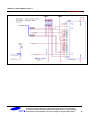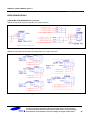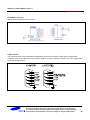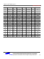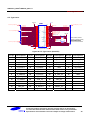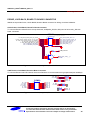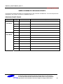
1
User’s Manual (SMDK2416) S3C2416X RISC Microprocessor Mar 17, 2008 Preliminary REV 0.0 Preliminary product information describe products that are in development, for which full characterization data and associated errata are not yet available. Specifications and information herein are subject to change without notice. Confidential Proprietary of Samsung Electronics Co., Ltd Copyright © 2007 Samsung Electronics, Inc. All Rights Reserved 1 SMDK2416_USER’S MANUAL_REV 0.0 Samsung Confidential Important Notice The information in this publication has been carefully checked and is believed to be entirely accurate at the time of publication. Samsung assumes no responsibility, however, for possible errors or omissions, or for any consequences resulting from the use of the information contained herein. Samsung reserves the right to make changes in its products or product specifications with the intent to improve function or design at any time and without notice and is not required to update this documentation to reflect such changes. This publication does not convey to a purchaser of semiconductor devices described herein any license under the patent rights of Samsung or others. Samsung makes no warranty, representation, or guarantee regarding the suitability of its products for any particular purpose, nor does Samsung assume any liability arising out of the application or use of any product or circuit and specifically disclaims any and all liability, including without limitation any consequential or incidental damages. "Typical" parameters can and do vary in different applications. All operating parameters, including "Typicals" must be validated for each customer application by the customer's technical experts. Samsung products are not designed, intended, or authorized for use as components in systems intended for surgical implant into the body, for other applications intended to support or sustain life, or for any other application in which the failure of the Samsung product could create a situation where personal injury or death may occur. Should the Buyer purchase or use a Samsung product for any such unintended or unauthorized application, the Buyer shall indemnify and hold Samsung and its officers, employees, subsidiaries, affiliates, and distributors harmless against all claims, costs, damages, expenses, and reasonable attorney fees arising out of, either directly or indirectly, any claim of personal injury or death that may be associated with such unintended or unauthorized use, even if such claim alleges that Samsung was negligent regarding the design or manufacture of said product S3C2416 RISC Microprocessor SMDK2416 User’s manual, Preliminary Revision 0.0 Copyright © 2007-2008 Samsung Electronics Co.,Ltd. All rights reserved. No part of this publication may be reproduced, stored in a retrieval system, or transmitted in any form or by any means, electric or mechanical, by photocopying, recording, or otherwise, without the prior written consent of Samsung Electronics Co.,Ltd. Samsung Electronics Co., Ltd. San #24 Nongseo-Dong, Giheung-Gu Yongin-City Gyeonggi-Do, Korea 446-711 Home Page: http://www.samsungsemi.com/ E-Mail: mobilesol.cs@samsung.com Printed in the Republic of Korea Preliminary product information describe products that are in development, for which full characterization data and associated errata are not yet available. Specifications and information herein are subject to change without notice. SMDK2416_USER’S MANUAL_REV 0.0 Samsung Confidential Revision History Revision No 0.0 Description of Change - Initial Release Refer to - Author(s) Date Mar 17, 2008 NOTE: Revised parts are written in blue. Preliminary product information describe products that are in development, for which full characterization data and associated errata are not yet available. Specifications and information herein are subject to change without notice. SMDK2416_USER’S MANUAL_REV 0.0 Samsung Confidential Table of contents SYSTEM OVERVIEW ................................................................................................................ 1 Features ...................................................................................................................................................................................... 3 CIRCUIT DESCRIPTION ....................................................................................................................................................... 4 SMDK2416 SYSTEM CONFIGURATIONS REV0.0 .................................................................. 9 Clock Source SELECTION ...................................................................................................................................................... 9 Boot Mode SELECTION ........................................................................................................................................................ 10 1. NAND Boot................................................................................................................................................................... 10 2. Muxed OneNAND Boot............................................................................................................................................... 10 3. JTAG Mode .................................................................................................................................................................. 11 4. AMD NOR/SROM Boot .............................................................................................................................................. 11 5. Internal ROM Boot...................................................................................................................................................... 12 Configuration switch description in CPU Board .................................................................................................................. 13 CFG4 _CPU: FOR USING SDRAM, MOBILE DDR SDRAM, DDR2 SDRAM.......................................................... 13 CFG5 _CPU: FOR USING HS-SPI.................................................................................................................................... 13 Configuration switch description in BASE Board ................................................................................................................ 14 CFG2_BASE : SROM BANK0 SELECTOR .................................................................................................................... 14 CFG3_BASE : SROM BANK1 SELECTOR .................................................................................................................... 14 CFG4_BASE: FOR USING IIC ......................................................................................................................................... 15 CFG7_BASE : IIS0 CLOCK(CDCLK) SELECTOR....................................................................................................... 15 CFG8 _BASE: IIS1 CLOCK(CDCLK) SELECTOR....................................................................................................... 15 CFG10 & CFG11_BASE : IIS & PCM EXTERNAL CLOCK SELECTOR ................................................................ 16 CFG6_BASE : MIC INDIRECTION SELECTOR .......................................................................................................... 16 CFG12_BASE : MIC BIAS SOURCE SELECTOR ........................................................................................................ 16 CFG5 _BASE: AUDIO ENABLE SELECTOR & DEMUX SELECTOR..................................................................... 17 CFG9 _BASE: UART SELECTOR ................................................................................................................................... 17 JUMPER SETTING CONFIGURATION ............................................................................................................................ 18 J23: OP3 POWER SELECT (CPU BOARD)................................................................................................................... 18 J4: SPI CONNECTION SELECT (BASE BOARD) ...................................................................................................... 18 J5: LCD INTERFACE SELECT (BASE BOARD) ......................................................................................................... 18 CONNECTORS ........................................................................................................................ 19 CPU BOARD TYPE1 REV0.0................................................................................................................................................ 19 JTAG......................................................................................................................................................................................... 19 USB........................................................................................................................................................................................ 19 Hi Speed – SPI...................................................................................................................................................................... 20 SD/MMC host (Ver1.0) High speed MMC interface ........................................................................................................ 20 Preliminary product information describe products that are in development, for which full characterization data and associated errata are not yet available. Specifications and information herein are subject to change without notice. SMDK2416_USER’S MANUAL_REV 0.0 Samsung Confidential BASE BOARD REV0.0 ........................................................................................................................................................... 23 LINE IN, MIC IN & SPEAKER OUT connector ............................................................................................................. 23 ETHERNET connector ....................................................................................................................................................... 24 UART interface .................................................................................................................................................................... 24 ADC connector..................................................................................................................................................................... 25 xD Picture Card Connector ................................................................................................................................................ 26 External SPI connector ....................................................................................................................................................... 27 TFT LCD Connector ........................................................................................................................................................... 28 Touch Screen ........................................................................................................................................................................ 30 EXTERNAL CONNECTOR INTERFACE.......................................................................................................................... 31 ROM BUS Interface ............................................................................................................................................................ 31 CF+ Type II Con. ................................................................................................................................................................. 33 PROBE, LOOP-BACK, BOARD TO BOARD CONNECTOR .......................................................................................... 34 SMDK 2416 provides Probe, LOOP-BACK, Board to Board connector for debug, functional validation. ................... 34 Audio Probe, LOOP-BACK, Board To Board connector ................................................................................................ 34 UART Probe, LOOP-BACK, Board to Board connector ................................................................................................ 34 REVISION POINTS TABLE ................................................................................................................................................. 35 SMDK SCHEMATIC................................................................................................................. 36 Preliminary product information describe products that are in development, for which full characterization data and associated errata are not yet available. Specifications and information herein are subject to change without notice. SMDK2416_USER’S MANUAL_REV 0.0 Samsung Confidential FIGURE INDEX Figure 1 S3C2416 Block Diagram ..............................................................................................................2 Figure 2 SMDK2416 Power Plane ...............................................................................................................4 Figure 3 SMDK2416 Board Diagram ...........................................................................................................5 Figure 4 SMDK2416 CPU Board Type1 real view......................................................................................6 Figure 5 SMDK2416 BASE Board real view (TOP) .....................................................................................7 Figure 6 SMDK2416 BASE Board real view (BOTTOM) .............................................................................8 Figure 7 JTAG Connector ..........................................................................................................................19 Figure 8 Dual USB ports & OTG port.........................................................................................................19 Figure 9 Hi Speed SPI socket(IEEE1394 type) .........................................................................................20 Figure 10 8 Bit SD card Socket..................................................................................................................20 Figure 11 4 Bit SD card Socket..................................................................................................................21 Figure 12 External ONE-NAND B’d Connector .........................................................................................22 Figure 13 Audio Line In, Mic In Connector................................................................................................23 Figure 14 I2S & PCM & AC97 OUT Socket ...............................................................................................23 Figure 15 Ethernet Socket .........................................................................................................................24 Figure 16 UART Sockets ...........................................................................................................................24 Figure 17 ADC Connector..........................................................................................................................25 Figure 18 xD Picture Card Socket .............................................................................................................26 Figure 19 External SPI Connector .............................................................................................................27 Figure 20 TFT LCD Connector (4.8”).........................................................................................................28 Figure 21 TFT LCD Connector (3.5”).........................................................................................................29 Figure 22 TFT LCD CPU & RGB Type Connector (2.22”).........................................................................30 Figure 23 Touch Screen Connector...........................................................................................................30 Figure 24 External ROM Bus Connector ...................................................................................................31 Figure 25 CF+ Type II Con. (SOCKET) .....................................................................................................33 Figure 26 Audio Probe, Loop-back, Board to Board Connector ................................................................34 Figure 27 Uart Probe, Loop-back, Board to Board Connector ..................................................................34 Preliminary product information describe products that are in development, for which full characterization data and associated errata are not yet available. Specifications and information herein are subject to change without notice. SMDK2416_USER’S MANUAL_REV 0.0 Samsung Confidential ABOUT SMDK2416 BOARD VER 0.0 SMDK2416 CPU and Base board revision number. CPU Board Version Rev 0.0 Base Board Version Rev 0.0 SYSTEM OVERVIEW This user’s manual describes SAMSUNG's S3C2416 16/32-bit RISC microprocessor. SAMSUNG’s S3C2416 is designed to provide hand-held devices and general applications with low-power, and high-performance micro-controller solution in small die size. To reduce total system cost, the S3C2416 includes the following components. The S3C2416 is developed with ARM926EJ core, 65nm CMOS standard cells and a memory complier. Its low-power, simple, elegant and fully static design is particularly suitable for cost- and power-sensitive applications. It adopts a new bus architecture known as Advanced Micro controller Bus Architecture (AMBA). The S3C2416 offers outstanding features with its CPU core, a 16/32-bit ARM926EJ RISC processor designed by Advanced RISC Machines, Ltd. The ARM926EJ implements MMU, AMBA BUS, and Harvard cache architecture with separate 16KB instruction and 16KB data caches, each with an 8-word line length. By providing a complete set of common system peripherals, the S3C2416 minimizes overall system costs and eliminates the need to configure additional components. The integrated on-chip functions that are described in this document include: Preliminary product information describe products that are in development, for which full characterization data and associated errata are not yet available. Specifications and information herein are subject to change without notice. 1 SMDK2416_USER’S MANUAL_REV 0.0 Samsung Confidential S3C2416 OVERVIEW The S3C2416 (2416 Development Kit) highlights the basic system-based hardware design which uses the S3C2416. It can evaluate the basic operations of the S3C2416 and assist in developing codes. S3C2416 is manufactured by MERITECH Co., Ltd and company website is www.mcukorea.com Figure 1 S3C2416 Block Diagram Preliminary product information describe products that are in development, for which full characterization data and associated errata are not yet available. Specifications and information herein are subject to change without notice. 2 SMDK2416_USER’S MANUAL_REV 0.0 Samsung Confidential FEATURES The features of SMDK2416 include: - S3C2416 : 16/32 bit RISC microcontroller - X-tal operation or oscillator - Boot Device : AMD 8Mbit 1EA - SAMSUNG NAND flash 1EA(socket) - SAMSUNG OneNAND 1EA(External Board) - Internal ROM - SDRAM : 64MB mDDR(K4X51163) 64MB DDR2(K4T51163QC) 64MB mSDR(K4S51323PF) - JTAG port - RTC X-tal input - QVGA, WVGA LCD & Touch panel interface - ADC interface - USB Host, USB OTG 2.0 interface - High Speed MMC interface - High Speed SPI interface - 2 port UART interface(including IrDA) - IIS/AC97/PCM Interface : WM9714, WM8753, WM8580 - EINT interface - Ethernet Interface : CS8900, LAN9115 - CF/ATA interface - Keypad interface - SD/MMC interface - XD Card interface - External PMIC Module Preliminary product information describe products that are in development, for which full characterization data and associated errata are not yet available. Specifications and information herein are subject to change without notice. 3 SMDK2416_USER’S MANUAL_REV 0.0 Samsung Confidential CIRCUIT DESCRIPTION POWER SUPPLY Figure 2 SMDK2416 Power Plane Preliminary product information describe products that are in development, for which full characterization data and associated errata are not yet available. Specifications and information herein are subject to change without notice. 4 SMDK2416_USER’S MANUAL_REV 0.0 Samsung Confidential BOARD DIAGRAM Figure 3 SMDK2416 Board Diagram Preliminary product information describe products that are in development, for which full characterization data and associated errata are not yet available. Specifications and information herein are subject to change without notice. 5 SMDK2416_USER’S MANUAL_REV 0.0 Samsung Confidential SMDK2416 CPU BOARD TYPE1 REAL VIEW JTAG SPI USB USB Host Device USB Mini CFG7 External I/O CFG3 CFG2 CFG5 SD0/MMC0 CFG4 CFG1 SD1/MMC1 CFG6 ONENAND Figure 4 SMDK2416 CPU Board Type1 real view Preliminary product information describe products that are in development, for which full characterization data and associated errata are not yet available. Specifications and information herein are subject to change without notice. 6 SMDK2416_USER’S MANUAL_REV 0.0 Samsung Confidential SMDK2416 BASE BOARD REAL VIEW CAMERA UART0 EXT LCD UART1/2/3 CFG4 CFG9 ETHERNET EXT LCD ETHERNET CON24 CFG5 CON29 CON7 CON9 MIC IN LINE IN CFG3 CFG2 CFG1 I2S1/PCM OUT AC97 OUT I2S REAR I2S CENTER xD card I2S FRONT EXT ROM BUS Figure 5 SMDK2416 BASE Board real view (TOP) Preliminary product information describe products that are in development, for which full characterization data and associated errata are not yet available. Specifications and information herein are subject to change without notice. 7 SMDK2416_USER’S MANUAL_REV 0.0 Samsung Confidential CFG7 CFG10 CON3 CF CON CFG11 CFG8 CFG6 CFG12 CON11 3.5” LCD CON Figure 6 SMDK2416 BASE Board real view (BOTTOM) Preliminary product information describe products that are in development, for which full characterization data and associated errata are not yet available. Specifications and information herein are subject to change without notice. 8 SMDK2416_USER’S MANUAL_REV 0.0 Samsung Confidential SMDK2416 SYSTEM CONFIGURATIONS rev0.0 Configuration switch (Dipswitch) 1 ――→ 2 ――→ 3 ――→ 4 ――→ Off ――→On CLOCK SOURCE SELECTION EXTCLK or X-TAL can be selected for the S3C2416 system clock by setting the XOM[0] values. The Clock Source selection must be X-tal Clock (CFG2[1] on CPU Board). Description CFG2[1]_CPU : XOM[0] External Oscillator Clock ON X-tal Clock OFF CFG3[1:4]_CPU Description [1] [2] [3] [4] External Oscillator Clock ON OFF OFF ON X-tal Clock OFF ON ON OFF Preliminary product information describe products that are in development, for which full characterization data and associated errata are not yet available. Specifications and information herein are subject to change without notice. 9 SMDK2416_USER’S MANUAL_REV 0.0 Samsung Confidential BOOT MODE SELECTION 1. NAND Boot A. Set CFG0 on CPU Board, Select NAND Type B. Set CFG1 on Base Board, Select NAND flash or XD Picture card CFG2[2:6]_CPU : XOM[1]~ XOM[4] Description [2] [3] [4] [5] Normal NAND, 512-byte page, 3 addr. Cycle OFF ON ON OFF Normal NAND, 512-byte page, 4 addr. Cycle ON ON ON OFF Advanced NAND, 2K-byte page, 4 addr. Cycle OFF ON OFF OFF Advanced NAND, 2K-byte page, 5 addr. Cycle ON ON OFF OFF Advanced NAND, 4K-byte page, 4 addr. Cycle OFF OFF OFF OFF Advanced NAND, 4K-byte page, 5 addr. Cycle ON OFF OFF OFF Note. NAND Boot is connected on nFCE. It is selected one between NAND Flash and XD Picture card. CFG1 [1:2] _CPU Description [1] [2] Connected NandFlash to B_nFCE ON OFF Connected XD Picture Card to B_nFCE OFF ON 2. Muxed OneNAND Boot A. Set CFG2 on CPU Board, Select OneNAND B. Set CFG1 on CPU Board, Select OneNAND C. SMDK2416 support external OneNAND Board, Connect it on J1 connecter on CPU Board Description CFG2 [2:5]_CPU Preliminary product information describe products that are in development, for which full characterization data and associated errata are not yet available. Specifications and information herein are subject to change without notice. 10 SMDK2416_USER’S MANUAL_REV 0.0 Samsung Confidential OneNAND (used External OneNAND B’d) [2] [3] [4] [5] ON OFF OFF ON Note. EXT_One NAND Boot is connected on nRCS0. It is selected one between EXT_One NAND Flash and AMD Flash or SRAM or EXT Device. CFG1 [1:2]_CPU Description [1] [2] Connected EXT_One NAND to nRCS0 ON OFF Connected AMD or SRAM or EXT to nRCS0 OFF ON 3. JTAG Mode A. Set CFG2 on CPU Board, Select JTAG Mode CFG2[1:5]_CPU Description JTAG Mode [1] [2] [3] [4] [5] ON OFF OFF OFF ON 4. AMD NOR/SROM Boot A. Set CFG2 on CPU Board, Select Data width B. Set CFG2 on Base Board, Select NOR flash CFG2[2:5]_CPU Description [2] [3] [4] [5] NOR Boot ( 8bit Data Width) OFF ON OFF ON NOR Boot (16bit Data Width) ON ON OFF ON Preliminary product information describe products that are in development, for which full characterization data and associated errata are not yet available. Specifications and information herein are subject to change without notice. 11 SMDK2416_USER’S MANUAL_REV 0.0 Samsung Confidential CFG2[1:4]_BASE Description [1] [2] [3] [4] Connected NOR Flash to B_SROM_nCS0 ON OFF OFF Don’t Care Connected EXT to B_SROM_nCS0 OFF ON OFF Don’t Care Connected SRAM to B_SROM_nCS0 OFF OFF ON Don’t Care Note. NOR Boot is connected to Bank0. Only NOR Flash can be used for NOR Boot 5. Internal ROM Boot A. Set CFG2 on CPU board, Select Internal ROM Boot B. Set CFG7_CPU to select Boot Device CFG2[1:5]_CPU Description JTAG Mode [1] [2] [3] [4] [5] Don’t Care OFF OFF ON OFF CFG7[1:4]_CPU Description [1] [2] [3] [4] MMC (Movi / iNAND) OFF OFF OFF Don’t Care NAND 512 Page 3 Addr. OFF ON OFF Don’t Care NAND 512 Page 4 Addr. ON ON OFF Don’t Care NAND 2048 Page 4 Addr. OFF OFF ON Don’t Care NAND 2048 Page 5 Addr. ON OFF ON Don’t Care NAND 4096 Page 5 Addr. OFF ON ON Don’t Care Preliminary product information describe products that are in development, for which full characterization data and associated errata are not yet available. Specifications and information herein are subject to change without notice. 12 SMDK2416_USER’S MANUAL_REV 0.0 Samsung Confidential CONFIGURATION SWITCH DESCRIPTION IN CPU BOARD CFG4 _CPU: FOR USING SDRAM, MOBILE DDR SDRAM, DDR2 SDRAM CFG4 component is used to select SDRAM, MOBILE DDR SDRAM, DDR2 SDRAM. Using 6 switches in this component, appropriate SDRAM type can be selected. CFG4[1:6]_CPU Description [1] [2] [3] [4] [5] [6] Connected SDRAM to nCS0 ON OFF OFF OFF OFF OFF Connected Mobile DDR SDRAM to nCS0 OFF ON OFF OFF OFF OFF Connected DDR2 SDRAM to nCS0 OFF OFF ON OFF OFF OFF Connected SDRAM to nCS1 OFF OFF OFF ON OFF OFF Connected Mobile DDR SDRAM to nCS1 OFF OFF OFF OFF ON OFF Connected DDR2 SDRAM to nCS1 OFF OFF OFF OFF OFF ON CFG5 _CPU: FOR USING HS-SPI CFG5 component is used to select HS-SPI Port. Using 2 switches in this component, appropriate HS-SPI can be selected. CFG5[1:4]_CPU Description [1] [2] [3] [4] LCD_INIT(HS-SPI0 to HS-SPI1) ON ON ON ON HS-SPI0 to CON4 (For B’d to B’d Connection) OFF OFF OFF OFF Preliminary product information describe products that are in development, for which full characterization data and associated errata are not yet available. Specifications and information herein are subject to change without notice. 13 SMDK2416_USER’S MANUAL_REV 0.0 Samsung Confidential CONFIGURATION SWITCH DESCRIPTION IN BASE BOARD CFG2_BASE : SROM BANK0 SELECTOR CFG2 component is used to select devices as SROM BUS I/F 0(B_SROM_nCS0). CFG2[1:3]_Base Description [1] [2] [3] NOR(AMD) Flash ON OFF OFF External Device OFF ON OFF SRAM OFF OFF ON CFG3_BASE : SROM BANK1 SELECTOR CFG3 component is used to select devices as SROM BUS I/F 1(B_SROM_nCS1). CFG3[1:6]_Base Description [1] [2] [3] [4] [5] [6] NOR (AMD) Flash ON OFF OFF OFF OFF OFF NAND Flash OFF ON OFF OFF OFF OFF XD Picture Card OFF OFF ON OFF OFF OFF External Device OFF OFF OFF ON OFF OFF SRAM OFF OFF OFF OFF ON OFF CS8900 OFF OFF OFF OFF OFF ON Preliminary product information describe products that are in development, for which full characterization data and associated errata are not yet available. Specifications and information herein are subject to change without notice. 14 SMDK2416_USER’S MANUAL_REV 0.0 Samsung Confidential CFG4_BASE: FOR USING IIC CFG4 used to select IIC0 or IIC1. CFG4[1:4]_Base Description [1] [2] [3] [4] For using IIC0 ON OFF ON OFF For using IIC1 OFF ON OFF ON CFG7_BASE : IIS0 CLOCK(CDCLK) SELECTOR CFG7 component is used to select IIS0 CDCLK Selector. CFG7[1:2]_Base Description [1] [2] I2S0 Master OFF ON I2S0 Slave OFF OFF I2S0 Master External Clock ON OFF CFG8 _BASE: IIS1 CLOCK(CDCLK) SELECTOR CFG8 component is used to select IIS1 CDCLK Selector. CFG8[1:3]_Base Description [1] [2] [3] I2S1 Master OFF ON OFF I2S1 Slave OFF OFF ON I2S1 Master External Clock ON OFF ON Preliminary product information describe products that are in development, for which full characterization data and associated errata are not yet available. Specifications and information herein are subject to change without notice. 15 SMDK2416_USER’S MANUAL_REV 0.0 Samsung Confidential CFG10 & CFG11_BASE : IIS & PCM EXTERNAL CLOCK SELECTOR CFG10 & CFG11 component is used to select IIS Clock & PCM Clock. IIS External Clock & PCM External Clock. For IIS, IIS CDCLK Selector should be set as Master External Clock. OSC1 is designated typically for the 96KHz, PCM data and OSC2 is designated for 44.1KHz PCM data. Number CFG10_Base (To) CFG11_Base (From) [1] IIS0 OSC1(36.864MHz) [2] PCM0 OSC2(16.9344MHz) [3] IIS1 8580 PLL Clock [4] PCM1 8753 PLL Clock CFG6_BASE : MIC INDIRECTION SELECTOR CFG6 component is used to select MIC Indirection. CFG6[1:2]_Base Description [1] [2] IIS1 PCM8753 ON OFF AC9714 OFF ON CFG12_BASE : MIC BIAS SOURCE SELECTOR CFG12 component is used to select MIC Bias source. To select MIC bias from Codec, appropriate Codec setting is needed. CFG12[1:4]_Base Description [1] [2] [3] [4] VTG Div. ON OFF OFF Don’t Care 8753 Codec OFF ON OFF Don’t Care 9714 Codec OFF OFF ON Don’t Care Preliminary product information describe products that are in development, for which full characterization data and associated errata are not yet available. Specifications and information herein are subject to change without notice. 16 SMDK2416_USER’S MANUAL_REV 0.0 Samsung Confidential CFG5 _BASE: AUDIO ENABLE SELECTOR & DEMUX SELECTOR CFG5 component is used to select Audio Demux. Audio 0 port are composed of IIS0, AC97 and PCM0, and Audio 1 port are composed of IIS1, PCM1. Selecting one Audio IP is possible among port0 and port 1 , but also Selecting one Audio IP from port0, selecting one Audio IP from port1 at same time is possible. (except the PCM0 & PCM1 case). Before enabling Audio 1 port, CFG6_CPU must be set accordingly. CFG5_Base Description [1] [4] Audio 0 Enable OFF ON Audio 1 Enable ON OFF CFG5[1:6]_Base Description [1] [2] [3] [4] [5] [6] IIS0 OFF OFF Don’t Care ON Don’t Care Don’t Care AC97 OFF ON OFF ON Don’t Care Don’t Care PCM0 OFF ON ON ON Don’t Care ON IIS1 ON Don’t Care Don’t Care OFF OFF Don’t Care PCM1 ON Don’t Care Don’t Care OFF ON OFF CFG9 _BASE: UART SELECTOR CFG9 component is used to select UARTs. One of UART1~3 is selectable, (or none of them). IrDA is multiplexed with UART2, So simultaneously selecting with Uart1 or Uart3 or none is possible. Usually UART1 is used for debug port. So prior to changing port, please change uart0 to debug port, or vice versa, CFG9[1:4]_Base Description [1] [2] [3] [4] UART1(usually debug port) OFF Don’t Care Don’t Care Don’t Care UART2 ON OFF OFF Don’t Care UART3 ON ON Don’t Care Don’t Care IrDA Don’t Care ON ON Don’t Care Preliminary product information describe products that are in development, for which full characterization data and associated errata are not yet available. Specifications and information herein are subject to change without notice. 17 SMDK2416_USER’S MANUAL_REV 0.0 Samsung Confidential JUMPER SETTING CONFIGURATION J23: OP3 POWER SELECT (CPU BOARD) OP3_3.3V OP3_1.8V J4: SPI CONNECTION SELECT (BASE BOARD) LCD_SPI EXT_SPI Note. * If you select EXT_SPI, It will be connected with CON9 CONNECTOR. J5: LCD INTERFACE SELECT (BASE BOARD) RGB Interface (LTS222) CPU Interface (LTS222) Preliminary product information describe products that are in development, for which full characterization data and associated errata are not yet available. Specifications and information herein are subject to change without notice. 18 SMDK2416_USER’S MANUAL_REV 0.0 Samsung Confidential CONNECTORS CPU BOARD TYPE1 REV0.0 JTAG Part Name: J2 (CPU) Figure 7 JTAG Connector USB Two Dual USB ports A-type (CON2A & CON2B, HOST) and one USB OTG port CON3 B Type and mini ABtype(CON11- TP)are supported by the SMDK 2416. Figure 8 Dual USB ports & OTG port Preliminary product information describe products that are in development, for which full characterization data and associated errata are not yet available. Specifications and information herein are subject to change without notice. 19 SMDK2416_USER’S MANUAL_REV 0.0 Samsung Confidential Hi Speed – SPI IEEE-1394 connector is used as a Hi Speed- SPI connecter Figure 9 Hi Speed SPI socket(IEEE1394 type) SD/MMC host (Ver1.0) High speed MMC interface SD (MMC) is provided by the 2416 and SD card socket (U17) is supported in the SMDK 2416 Figure 10 8 Bit SD card Socket Preliminary product information describe products that are in development, for which full characterization data and associated errata are not yet available. Specifications and information herein are subject to change without notice. 20 SMDK2416_USER’S MANUAL_REV 0.0 Samsung Confidential Figure 11 4 Bit SD card Socket Preliminary product information describe products that are in development, for which full characterization data and associated errata are not yet available. Specifications and information herein are subject to change without notice. 21 SMDK2416_USER’S MANUAL_REV 0.0 Samsung Confidential EXTERNAL ONE-NAND connector External connector is supported for connecting ONE_NAND external board Figure 12 External ONE-NAND B’d Connector Preliminary product information describe products that are in development, for which full characterization data and associated errata are not yet available. Specifications and information herein are subject to change without notice. 22 SMDK2416_USER’S MANUAL_REV 0.0 Samsung Confidential BASE BOARD REV0.0 LINE IN, MIC IN & SPEAKER OUT connector SMDK 2416 provides LINE IN, MIC IN as an audio connector Figure 13 Audio Line In, Mic In Connector SMDK 2416 provides I2S and AC97 and PCM OUT as an audio connector. Figure 14 I2S & PCM & AC97 OUT Socket Preliminary product information describe products that are in development, for which full characterization data and associated errata are not yet available. Specifications and information herein are subject to change without notice. 23 SMDK2416_USER’S MANUAL_REV 0.0 Samsung Confidential ETHERNET connector SMDK 2416 provides Ethernet connector. Figure 15 Ethernet Socket UART interface The S3C2416 UART unit provides three independent asynchronous serial I/O (SIO) ports including IrDA. In SMDK 2416 board, COM1 port is only used for UART0. No jumper setting is required. You can change UART by setting related jumpers. Figure 16 UART Sockets Preliminary product information describe products that are in development, for which full characterization data and associated errata are not yet available. Specifications and information herein are subject to change without notice. 24 SMDK2416_USER’S MANUAL_REV 0.0 Samsung Confidential ADC connector Figure 17 ADC Connector Preliminary product information describe products that are in development, for which full characterization data and associated errata are not yet available. Specifications and information herein are subject to change without notice. 25 SMDK2416_USER’S MANUAL_REV 0.0 Samsung Confidential xD Picture Card Connector SMDK 2416 provides xD Picture Card Connector. Figure 18 xD Picture Card Socket Preliminary product information describe products that are in development, for which full characterization data and associated errata are not yet available. Specifications and information herein are subject to change without notice. 26 SMDK2416_USER’S MANUAL_REV 0.0 Samsung Confidential External SPI connector SMDK 2416 provides External SPI connector which can be selected by setting J4 jumper. Figure 19 External SPI Connector Preliminary product information describe products that are in development, for which full characterization data and associated errata are not yet available. Specifications and information herein are subject to change without notice. 27 SMDK2416_USER’S MANUAL_REV 0.0 Samsung Confidential TFT LCD Connector TFT LCD controllers are equipped in the S3C2450X. TFT LCD, touch panel and LCD backlight driver are supported in the SMDK 2416. Part Name CON12 CON11 CON13 CON14 Model Name LTE480WV-F01 LTV350QV_F06 LTS222QV-F01 LTS222QV-F01 Panel Size(pixels) 4.8”(800x480) 3.5”(320x240) 2.22”(240x320) 2.22”(240x320) I/F type 24bit RGB 24bit RGB + SPI 18/6bit RGB / 16bit i80 16bit i80 Back-Light Unit 14 LED(4pin) 6 LED(2pin) Connector type 45pin(0.5mm pitch) 60pin(0.5mm pitch) 4 LED(2pin) 40pin(0.5mm pitch) 4 LED(2pin) 40pin(0.5mm pitch) Figure 20 TFT LCD Connector (4.8”) Preliminary product information describe products that are in development, for which full characterization data and associated errata are not yet available. Specifications and information herein are subject to change without notice. 28 SMDK2416_USER’S MANUAL_REV 0.0 Samsung Confidential Figure 21 TFT LCD Connector (3.5”) Preliminary product information describe products that are in development, for which full characterization data and associated errata are not yet available. Specifications and information herein are subject to change without notice. 29 SMDK2416_USER’S MANUAL_REV 0.0 Samsung Confidential Figure 22 TFT LCD CPU & RGB Type Connector (2.22”) Touch Screen Part Name: CON15 (BASE) Figure 23 Touch Screen Connector Preliminary product information describe products that are in development, for which full characterization data and associated errata are not yet available. Specifications and information herein are subject to change without notice. 30 SMDK2416_USER’S MANUAL_REV 0.0 Samsung Confidential EXTERNAL CONNECTOR INTERFACE ROM BUS Interface Figure 24 External ROM Bus Connector Preliminary product information describe products that are in development, for which full characterization data and associated errata are not yet available. Specifications and information herein are subject to change without notice. 31 SMDK2416_USER’S MANUAL_REV 0.0 Samsung Confidential # of pin Descriptions # of pin Descriptions # of pin Descriptions # of pin Descriptions 1 VDD_3.3V 21 B_ADDR10 41 B_DATA0 61 SPI_KEYMIS O 2 VDD_3.3V 22 B_ADDR11 42 B_DATA1 62 SPI_KEYMOS I 3 nCS_EXT 23 B_ADDR12 43 B_DATA2 63 SPI_KEYnSS 4 PWREN_CF 24 B_ADDR13 44 B_DATA3 64 SPI_KEYCLK 5 B_nRWE 25 B_ADDR14 45 B_DATA4 65 nXBREQ 6 B_nROE 26 B_ADDR15 46 B_DATA5 66 nXBACK 7 GND 27 GND 47 B_DATA6 67 EINT2 8 GND 28 GND 48 B_DATA7 68 nRSTOUT 9 B_ADDR 0 29 B_ADDR16 49 GND 69 TOUT2 10 B_ADDR 1 30 B_ADDR17 50 GND 70 nWAIT 11 B_ADDR 2 31 B_ADDR18 51 B_DATA8 71 B_nRBE1 12 B_ADDR 3 32 B_ADDR19 52 B_DATA9 72 RXD_0 13 B_ADDR 4 33 B_ADDR20 53 B_DATA10 73 B_nRBE0 14 B_ADDR 5 34 B_ADDR21 54 B_DATA11 74 TXD_0 15 B_ADDR 6 35 B_ADDR22 55 B_DATA12 75 nXDACK0_I2 S0_SDO1 16 B_ADDR 7 36 B_ADDR23 56 B_DATA13 76 nXDREQ0_I2 S0_SDO2 17 GND 37 B_ADDR24 57 B_DATA14 77 nXDACK1_IIC SDA1 18 GND 38 B_ADDR25 58 B_DATA15 78 nXDREQ1_IIC SCL1 19 B_ADDR 8 39 GND 59 GND- 79 GND 20 B_ADDR 9 40 GND 60 GND 80 GND Preliminary product information describe products that are in development, for which full characterization data and associated errata are not yet available. Specifications and information herein are subject to change without notice. 32 SMDK2416_USER’S MANUAL_REV 0.0 Samsung Confidential CF+ Type II Con. VDD_CF B_DATA3 B_DATA4 B_DATA5 B_DATA6 B_DATA7 1,3,4,16 B_ADDR[25:0] B_ADDR101 nCS_CF0 16 B_nOE_CF B_ADDR9 B_ADDR8 B_ADDR7 1,3,4,16 B_DATA[15:0] TP6 CON3 1,3,4,16 B_DATA[15:0] B_ADDR6 B_ADDR5 B_ADDR4 B_ADDR3 B_ADDR2 B_ADDR1 B_ADDR0 B_DATA0 B_DATA1 B_DATA2 R45 10K CD2_CF 1 2 3 4 5 6 7 8 9 10 11 12 13 14 15 16 17 18 19 20 21 22 23 24 25 CD1 GND D11 D3 D12 D4 D13 D5 D14 D6 D15 D7 nCE2 nCE1 nVS1/GND A10 nIORD nOE nIOWR A9 nWE A8 IREQ A7 VCC VCC nCSEL A6 nVS2/OPEN A5 RESET A4 nWAIT A3 nINPACK A2 nREG A1 nSPKR A0 nSTSCHG D0 D8 D1 D9 D2 D10 WP GND CD2 26 27 28 29 30 31 32 33 34 35 36 37 38 39 40 41 42 43 44 45 46 47 48 49 50 B_DATA[15:0] 1,3,4,16 CD1_CF B_DATA11 B_DATA12 B_DATA13 B_DATA14 B_DATA15 nCS_CF1 1 B_nROE 1,3,4,16 B_nRWE 1,3,4,16 B_nWE_CF 16 nIRQ_CF 16 R41 R42 RESET_CF 16 nWAIT 3,16 nINPACK_CF 16 nREG_CF 16 R43 R44 VDD_CF 10K 10K RESET/RESET/nRESET 10K 10K B_DATA8 B_DATA9 B_DATA10 nINPACK/nINPACK/DREQ nREG/nREG/nDACK BVD2/nSPKR/nDASP BVD1/nSTSCHG/nPDIAG CF050-YAMAICHI Compact Flash CON Figure 25 CF+ Type II Con. (SOCKET) # of pin Descriptions # of pin Descriptions # of pin Descriptions # of pin Descriptions 1 GND 15 B_ADDR5 29 B_DATA13 43 nINPACK_CF 2 B_DATA3 16 B_ADDR4 30 B_DATA14 44 nREG_CF 3 B_DATA 4 17 B_ADDR3 31 B_DATA15 45 VDD_CF 4 B_DATA 5 18 B_ADDR2 32 nCF_CS1 46 VDD_CF 5 B_DATA 6 19 B_ADDR1 33 GND 47 B_DATA8 6 B_DATA 7 20 B_ADDR0 34 B_nROE 48 B_DATA9 7 nCF_CS0 21 B_DATA0 35 B_nRWE 49 B_DATA10 8 B_ADDR10 22 B_DATA1 36 B_nWE_CF 50 GND 9 B_nOE_CF 23 B_DATA2 37 nIRQ_CF 10 B_ADDR9 24 VDD_CF 38 VDD_CF 11 B_ADDR8 25 CD2_CF 39 GND 12 B_ADDR7 26 CD1_CF 40 - 13 VDD_CF 27 B_DATA11 41 RESET_CF 14 B_ADDR6 28 B_DATA 12 42 nWAIT Preliminary product information describe products that are in development, for which full characterization data and associated errata are not yet available. Specifications and information herein are subject to change without notice. 33 SMDK2416_USER’S MANUAL_REV 0.0 Samsung Confidential PROBE, LOOP-BACK, BOARD TO BOARD CONNECTOR SMDK 2416 provides Probe, LOOP-BACK, Board to Board connector for debug, functional validation. Audio Probe, LOOP-BACK, Board To Board connector To connect between I2S0 and I2S1 for loop-back test, AND(I2S0_SD,SD1,SD2) can be fed to I2S1_SDI with R304 connected. for loopback, b'd to b'd, & waveform observe CON12B (N.C) 1 7 I2S1_SCLK_PCM1_SCLK 16 2 8 I2S1_CDCLK_PCM1_CDCLK 16 3 9 I2S1_LRCK_PCM1_FSY NC 16 4 10 I2S1_SDO_PCM1_SDO 16 5 11 I2S1_SDI_PCM1_SDI 16 6 12 I2S0_SDO_AND_0_1_2 CON24 16 I2S0_SCLK_PCM0_SCLK_AC_SY NC 16 I2S0_CDCLK_PCM0_CDCLK_AC_BIT_CLK 16 I2S0_LRCK_PCM0_FSY NC_AC_nRESET 16 I2S0_SDI_PCM0_SDI_AC_SDI 16 I2S0_SDO_PCM0_SDO_AC_SDO 2,12,16 nXDACK0_I2S0_SDO1 2,12,16 nXDREQ0_I2S0_SDO2 1 J15 2 JUMPER(N.C) R304 VDD_ext3.3V 2 0(NC) 6 3 1 4 I2S0_SDO_AND_0_1_2 SN74LVC1G11DBV 5 U49 Figure 26 Audio Probe, Loop-back, Board to Board Connector UART Probe, LOOP-BACK, Board to Board connector To connect between board and board, disconnect Resistors is recommended for high speed test(over 250kbps) R315 R316 2,16 TXD0 2,16 RXD0 R317 R318 CON29 16 CTS0 16 RTS0 2,16 TXD0 2,16 RXD0 16 TXD2 16 RXD2 1 2 3 4 5 6 7 8 9 10 11 12 CON12B (N.C) CTS1 RTS1 TXD1 RXD1 TXD3 RXD3 16 16 16 16 16 16 0 0 TXD1 16 RXD1 16 R319 R320 16 TXD2 16 RXD2 R321 R322 0 0 0 0 0 0 TXD3 16 RXD3 16 Figure 27 Uart Probe, Loop-back, Board to Board Connector Preliminary product information describe products that are in development, for which full characterization data and associated errata are not yet available. Specifications and information herein are subject to change without notice. 34 SMDK2416_USER’S MANUAL_REV 0.0 Samsung Confidential SMDK SCHEMATIC REVISION POINTS This document contains information of corrected points on the schematic of SMDK2416. The corrected points are highlighted in red-circled in schematic of SMDK2416 Rev 0.0 REVISION POINTS TABLE Boards Page Contents Corrected points CPU Board Base Board Preliminary product information describe products that are in development, for which full characterization data and associated errata are not yet available. Specifications and information herein are subject to change without notice. 35 SMDK2416_USER’S MANUAL_REV 0.0 Samsung Confidential SMDK SCHEMATIC There are 2 parts of SMDK2416 Schematic. 1. CPU Board 2. Base Board Note. It is easy to find schematic parts by using Bookmarks on PDF Preliminary product information describe products that are in development, for which full characterization data and associated errata are not yet available. Specifications and information herein are subject to change without notice. 36