1
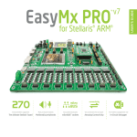
All MikroElektronika´s development systems represent irreplaceable tools for
programming and developing microcontroller-based devices. Carefully chosen
components and the use of machines of the last generation for mounting and
testing thereof are the best guarantee of high reliability of our devices. Due to
simple design, a large number of add-on modules and ready to use examples,
all our users, regardless of their experience, have the possibility to develop
their project in a fast and efficient way.
User manual
Development System
If you have any questions, comments or business proposals, do not hesitate to contact us at office@mikroe.com
If you are experiencing some problems with any of our products or just need additional information, please place your ticket at
www.mikroe.com/en/support
If you want to learn more about our products, please visit our website at www.mikroe.com
LV32MX v6
™
DISCLAIMER
All the products owned by MikroElektronika are protected by copyright law and international copyright treaty.
Therefore, this manual is to be treated as any other copyright material. No part of this manual, including
product and software described herein, may be reproduced, stored in a retrieval system, translated or
transmitted in any form or by any means, without the prior written permission of MikroElektronika. The
manual PDF edition can be printed for private or local use, but not for distribution. Any modification of this
manual is prohibited.
TO OUR VALUED CUSTOMERS
I want to express my thanks to you for being interested in our products and for having confidence in
mikroElektronika.
The primary aim of our company is to design and produce high quality electronic products and to constantly
improve the performance thereof in order to better suit your needs.
Nebojsa Matic
General Manager
MikroElektronika provides this manual ‘as is’ without warranty of any kind, either expressed or implied,
including, but not limited to, the implied warranties or conditions of merchantability or fitness for a particular
purpose.
MikroElektronika shall assume no responsibility or liability for any errors, omissions and inaccuracies that may
appear in this manual. In no event shall MikroElektronika, its directors, officers, employees or distributors be
liable for any indirect, specific, incidental or consequential damages (including damages for loss of business
profits and business information, business interruption or any other pecuniary loss) arising out of the use
of this manual or product, even if MikroElektronika has been advised of the possibility of such damages.
MikroElektronika reserves the right to change information contained in this manual at any time without prior
notice, if necessary.
HIGH RISK ACTIVITIES
The products of MikroElektronika are not fault – tolerant nor designed, manufactured or intended for use or
resale as on – line control equipment in hazardous environments requiring fail – safe performance, such as
in the operation of nuclear facilities, aircraft navigation or communication systems, air traffic control, direct
life support machines or weapons systems in which the failure of Software could lead directly to death,
personal injury or severe physical or environmental damage (‘High Risk Activities’). MikroElektronika and its
suppliers specifically disclaim any expressed or implied warranty of fitness for High Risk Activities.
TRADEMARKS
The Mikroelektronika name and logo, the Mikroelektronika logo, mikroC, mikroC PRO, mikroBasic, mikroBasic PRO, mikroPascal, mikroPascal PRO, AVRflash, PICflash, dsPICprog, 18FJprog, PSOCprog, AVRprog, 8051prog, ARMflash, EasyPIC5, EasyPIC6, BigPIC5, BigPIC6, dsPIC PRO4, Easy8051B, EasyARM,
EasyAVR5, EasyAVR6, BigAVR2, EasydsPIC4A, EasyPSoC4, EasyVR Stamp LV18FJ, LV24-33A, LV32MX,
PIC32MX4 MultiMedia Board, PICPLC16, PICPLC8 PICPLC4, SmartGSM/GPRS, UNI-DS are trademarks
of Mikroelektronika. All other trademarks mentioned herein are property of their respective companies.
All other product and corporate names appearing in this manual may or may not be registered trademarks
or copyrights of their respective companies, and are only used for identification or explanation and to the
owners’ benefit, with no intent to infringe.
The Microchip name and logo, the Microchip logo, Accuron, dsPIC, KeeLoq, microID, MPLAB, PIC, PICmicro, PICSTART, PRO MATE,
PowerSmart, rfPIC and SmartShunt are registered trademarks of Microchip Technology Incorporated in the U.S.A and other countries.
©MikroelektronikaTM, 2011, All Rights Reserved.
3
page
LV32MX v6 Development System
TABLE OF CONTENTS
Introduction to LV32MX v6 Development System ............................................................................ 4
Key Features .................................................................................................................................... 5
1.0. Connecting the System to a PC ................................................................................................ 6
2.0. Supported Microcontrollers ....................................................................................................... 7
3.0. On-board PIC32Flash Programmer .......................................................................................... 9
4.0. ICD Connector ......................................................................................................................... 10
5.0. 3.3V Voltage Regulator ..............................................................................................................10
6.0. Power Supply ............................................................................................................................11
7.0. USB Communication Connector ...............................................................................................12
8.0. USB HOST Connector ...............................................................................................................12
9.0. USB UART Module ...................................................................................................................13
10.0. CAN Communication Module ..................................................................................................14
11.0. MMC/SD Connector ................................................................................................................15
12.0. Temperature Sensor ...............................................................................................................16
13.0. Joystick ...................................................................................................................................17
14.0. FLASH Module .......................................................................................................................18
15.0. EEPROM Module ...................................................................................................................18
16.0. Audio Module ..........................................................................................................................19
17.0. On-board 2x16 LCD ................................................................................................................21
18.0. TFT Display .............................................................................................................................22
19.0. LEDs ........................................................................................................................................23
20.0. Push Buttons ...........................................................................................................................24
21.0. I/O Ports ..................................................................................................................................25
MikroElektronika
page
4
LV32MX v6 Development System
Introduction to LV32MX v6 Development System
The LV32MX v6™ development system provides a development environment for experimenting with PIC32™ microcontrollers from
Microchip®. The system includes an on-board programmer PIC32Flash™ which serves as an interface between the microcontroller
and a PC. You are simply expected to write a program, generate a .hex file and program your microcontroller using the mikroPROG
Suite for PIC™ program. Numerous modules, such as TFT display with a resoultion of 320x240, on-board 2x16 LCD, serial EEPROM
module etc, are provided on the board and allow you to easily simulate the operation of the target device.
Full-featured development
system for PIC32MX
microcontroller based devices
On-board USB 2.0 programmer
TFT display provides a palette
of 262.000 colours and an
integrated touch panel
A possibility of reading
MMC/SD memory cards
Navigation joystick used for
easier orientation and navigation
through the user menu
The PIC32FLASH™ program for programming provides a complete list of all
supported microcontrollers. The latest version of this program with updated
list of supported microcontrollers can be downloaded from our website at
www.mikroe.com
Package contains:
Development system: LV32MX v6
CD:
product CD with relevant software
Cables:
USB cable
Documentation:
Manual for LV32MX v6, quick guide for installing USB drivers and electrical schematic of the system
System specification:
Power supply:
over an AC/DC connector (7-23V AC or 9-32V DC); or
over a USB cable for programming (5V DC)
Power consumption:~40mA in idle state when all on-board modules are off
Dimension:
26,5 x 22cm (10,4 x 8,6inch)
Weight:
440g (0.97lbs)
MikroElektronika
5
1
2
3
4
5
6
7
8
9
10
page
LV32MX v6 Development System
11
27
26
25
12
24
23
13
22
21
20
19
18 17
16
15
14
Key Features
1. On-board programmer PIC32Flash
2. Connector for external programmer ICD2® or ICD3®
3. Audio module
4. Speaker
5. USB communication connector
6. USB HOST connector
7. USB UART 1 module
8. USB UART 2 module
9. DIMM 168P socket for MCU cards
10. Jumper for pull-up/pull-down resistor selection
11. DIP switches enable pull-up/pull-down resistors
12. I/O port connectors
13. DIP switches turn on/off on-board modules
14. Navigation joystick
15. TFT display with integrated touch panel
16. Push buttons simulate microcontroller input pins
17. Jumper for shortening the protective resistor
18. Jumper for selecting push buttons’ logic state
19. Reset button
20. MMC/SD card connector
21. Power supply voltage regulator
22. 85 LEDs indicate pins’ logic state
23. CAN communication module
24. On-board 2x16 LCD
25. Temperature sensor
26. FLASH module
27. EEPROM module
MikroElektronika
page
6
LV32MX v6 Development System
1.0. Connecting the System to a PC
Step 1: Install mikroProg Suite for PIC
Follow the instructions provided in the relevant manual and install the mikroProg Suite for PIC program and the USB driver from the
product CD. They are essential for the proper operation of the on-board programmer.
Step 2: Connect development system
Use the USB cable to connect the development system to a PC. One end of the USB cable, with a USB connector of B type, should
be connected to the development system, as shown in Figure 1-2, whereas the other end of the cable with a USB connector of A
type should be connected to a PC. When establishing a connection, make sure that jumper J16 is placed in the USB position as
shown in Figure 1-1.
AC/DC connector
USB connector
1
2
J16 power supply selector
POWER SUPPLY switch
Figure 1-1: Power supply
Figure 1-2: Connecting USB cable
Step 3: Load .hex file
Turn on your development system by setting the POWER SUPPLY switch to ON position. Two LEDs marked as POWER and USB LINK
will be automatically turned on indicating that your development system is ready to use. Use the on-board programmer PIC32Flash and
the mikroProg Suite for PIC program to dump a code into the microcontroller and employ the system to test and develop your projects.
NOTE:
If some additional modules are used, it is necessary to place them properly on the development system while it is turned off. Otherwise, either can be permanently damaged. Refer to figure below for the proper placing of the additional modules.
Figure 1-3: Placing additional modules on the board
MikroElektronika
7
page
LV32MX v6 Development System
2.0. Supported Microcontrollers
The LV32MX v6 development system provides a DIMM-168P connector to place an MCU card into. This development system comes
with an MCU card with the PIC32MX460F512L in 100-pin TQFP package soldered on it, Figure 2-3. Besides, the MCU card alone
provides an oscillator as well as 102 soldering pads connected to microcontroller pins. Each pad is marked the same as the pin it is
connected to. Soldering pads also make connection between the MCU card and target device’s modules easy.
DIMM-168P
connector for placing
the MCU card with
microcontroller in
TQFP package
Figure 2-2: DIMM-168P connector with the MCU card inserted
Figure 2-1: DIMM-168P connector
Figure 2-3: MCU card with a 100-pin microcontroller in TQFP package soldered on it
Figure 2-4: Schematic of the DIMM-168P connector’s pinout
MikroElektronika
page
8
LV32MX v6 Development System
The MCU card should be placed into the DIMM-168P connector in the following way:
1
B
A
Open extraction levers A and B
2
Extraction levers for fixing
the MCU card in ‘open’
position
Insert the MCU card into the DIMM-168P connector
3
Push the MCU card down gently into the DIMM-168P connector and
lift extraction levers slowly at the same time
MikroElektronika
Extraction levers for fixing
the MCU card in ‘closed’
position
9
page
LV32MX v6 Development System
3.0. On-board PIC32Flash Programmer
A programmer is a necessary tool when working with microcontrollers. It is used to load a hex code into the microcontroller and serves
as an interface between the microcontroller and the PC. The LV32MX v6 has an on-board PIC32Flash programmer. The mikroProg
Suite for PIC program is used for loading a .hex file into the microcontroller. Figure 3-3 shows connection between the compiler,
MikroProg Suite for PIC program and the microcontroller.
Programmer’s USB connector
Programmer’s chip
Figure 3-2: USB connector’s front side
Figure 3-1: On-board programmer
1 Write a program and generate a
.hex file;
Compiling program
2 Use the PIC32FLASH program
to select desired microcontroller to be
programmed and load the .hex file;
3 Click the Write button to dump
the code into the microcontroller.
2
1
Write a code, generate a .hex file, and employ
the on-board PIC32Flash programmer to load the
code into the microcontroller.
Loading hex code
3
On the left side of the
PIC32FLASH program’s main
window, there are a number
of options for setting the
operation of the microcontroller
to be used. A number of options
which enable the programming
process are provided on the right
side of the window. Positioned
in the bottom right corner of
the window, the Progress bar
enables you to monitor the
programming progress.
Figure 3-3: Programming process
MikroElektronika
page
10
LV32MX v6 Development System
4.0. ICD Connector
In addition to the on-board PIC32Flash programmer, one of the external programmers ICD2 or ICD3 from Microchip can be used for
programming microcontrollers. Connection between the external programmer and development system is established by means of
the ICD connector.
mRST#
mRST#
RA0
RA2
RA4
RA6
RA1
RA3
RA5
RA7
RA10
RA9
RE9
RA14
RA15
CN18
RB0-MCU
RB2
RB4
RB6
RB1-MCU
RB3
RB5
RB7
RB1-MCU
RB0-MCU
GND
VCC-3.3
mRST#
1
2
3
4
5
6
RJ12
ICD
1 3 5
2 4 6
Front view
Side view
Bottom view
VCC-3.3
Figure 4-1: ICD connector
RB8
RB9
RB11
C42
100nF
Figure 4-2: ICD connector and microcontroller connection schematic
For the .hex file to be loaded into the microcontroller, it is necessary to provide an adequate program. The MPLAB program from Microchip
is the right one. You can use this program to write a code and load it afterwards into the microcontroller. By means of the Programmer
option, contained in the MPLAB window, you can select a programmer to be used for loading the code into the microcontroller.
5.0. 3.3V Voltage Regulator
The LV32MX v6 development system is provided with a voltage regulator whose purpose is to reduce the power supply voltage of
the development system from 5V to 3.3V. The 3.3V power supply voltage is then used for powering the microcontroller and other
on-board modules. The MC33269DT-3.3 circuit provided on the development system is used as a voltage regulator capable of
providing 800mA current.
Figure 5-2: Voltage regulator connection schematic
Figure 5-1: Voltage regulator
MikroElektronika
11
page
LV32MX v6 Development System
6.0. Power supply
The LV32MX v6 development system may use one of two power supply sources:
1. +5V PC power supply through the USB programming cable; and
2. External power supply source connected to an AC/DC connector provided on the development board.
The MC34063A voltage regulator and Gretz rectifier are used to enable external power supply voltage to be either AC (in the range of
7V to 23V) or DC (in the range of 9V to 32V). Jumper J16 is used as a selector of the power supply source. To take advantage of the
USB power supply, jumper J16 should be placed in the USB position. When using the external power supply, jumper J16 should be
placed in the EXT position. The development system is turned on/off by switching the position of the POWER SUPPLY switch.
AC/DC connector
Power supply
voltage regulator
USB connector
POWER SUPPLY signal LED
Jumper J16 as a
selector of the power
supply source
POWER SUPPLY switch
Figure 6-1: Power supply
Powering over an
AC/DC connector
Powering over a
USB connector
Figure 6-2: Power supply source connection schematic
MikroElektronika
page
12
LV32MX v6 Development System
7.0. USB Communication Connector
The CN21 USB connector enables a PIC32 microcontroller with a built-in USB communication module to be connected to peripheral
modules. The microcontroller is connected to the CN21 USB connector via USB-DM and USB-DP lines. The function of the LED
marked as ON is to indicate connection between USB devices and the development system, hence the microcontroller.
USB connector is connected to the microcontroller
Figure 7-1: USB connector
Figure 7-2: USB connector and microcontroller connection schematic
8.0. USB HOST Connector
The LV32MX v6 development system can be linked to peripheral units, such as printer, USB flash memory etc. by means of the USB
HOST connector. Communication between the microcontroller and USB devices is performed via RG2, RG3 and RB14 microcontroller
pins. The USB HOST connector is linked to the microcontroller via the same pins as the USB communication connector so that it is
not possible to use them simultaneously.
USB connector of A type is connected to the microcontroller
Figure 8-1: USB connector of A type
Figure 8-2: USB connector and microcontroller connection schematic
MikroElektronika
13
page
LV32MX v6 Development System
9.0. USB UART Modules
USB UART modules enable the development system to be connected to a PC via a USB connector. In addition to
PC, the development system can also be easily connected to other devices that use USB communication. USB UART
modules are connected to the microcontroller supplied on the development system via DIP switch SW15. In order to
establish connection between USB UART 1 module and MCU turn ON switches 1-4 on DIP switch SW15. For USB
UART 2 turn ON switches 5-8 on DIP switch SW15.
USB connector
Figure 9-1: USB UART modules
Port RS-232A is connected to the microcontroller
via RF2, RF8, RD14 and RD15 pins
U4
SW15
U1RX
U1TX
U1CTS#
U1RTS#
U2RX
U2TX
U2CTS#
U2RTS#
RF2
RF8
RD14
RD15
RF4
RF5
RF12
RF13
U1RX
TXD
VCC-3.3
U1CTS#
C31
C29
RTS#
TEST
100nF
100nF
VCCIO
AGND
RXD
RI#
CBUS1
CBUS1
DSR#
VCC
RESET#
CTS#
RB6
RB7
RA9
RA10
AVCC
AGND
RB8
RB9
RB10
RB11
GND
VCC
RA1
RF13
RF12
RB12
RB13
RB14
RB15
GND
VCC
RD14
RD15
RF4
RF5
VCC3
3V3OUT
CBUS2
USBDM
CBUS3
USBDP
FT232RL
FTDI1
R11
4K7
GND
CBUS4
VCC
DD+
GND
C38
CN12
USB B
R43
10K
100nF
VCC
PIC32MX460F512L
GND
RC14
RC13
RD0
RD11
RD10
RD9
RD8
RA15
RA14
GND
OSC2
OSC1
VCC
RA5
RA4
RA3
RA2
RG2
RG3
VUSB
VBUS
RF8
RF2
RF3
10uF
D-
RG15
VCC
RE5
RE6
RE7
RC1
RC2
RC3
RC4
RG6
RG7
RG8
MCLR
RG9
GND
VCC
RA0
RE8
RE9
RB5
RB4
RB3
RB2
RB1
RB0
E16
VCC-5V
D+ GND
VCC3
RE4
RE3
RE2
RG13
RG12
RG14
RE1
RE0
RA7
RA6
RG0
RG1
RF1
RF0
ENVREG
VCAP
RD7
RD6
RD5
RD4
RD13
RD12
RD3
RD2
RD1
VCC3
VCC-5V
GND
DCD#
U1RTS#
E9
10uF
NC
GND
NC
VCC3
VCC-5V
VCC-3.3
OSCO
OSCI
DTR#
U1TX
Bottom view
U5
U2RX
U2TX
VCC3
VCC-3.3
U2CTS#
TXD
VCC-5V
VCC-3.3
OSCO
DTR#
OSCI
C32
C30
RTS#
TEST
100nF
100nF
VCCIO
AGND
RXD
NC
RI#
CBUS1
GND
CBUS1
NC
DSR#
VCC
RESET#
CTS#
E17
GND
DCD#
U2RTS#
VCC-5V
VCC-5V
10uF
R39
4K7
GND
CBUS4
3V3OUT
CBUS2
USBDM
CBUS3
USBDP
VCC
DD+
GND
VCC3
FT232RL
USB B
D-
100nF
R54
10K
VCC
D+ GND
FTDI2
C39
CN13
Bottom view
Figure 9-2: USB UART modules and microcontroller connection schematic
MikroElektronika
page
14
LV32MX v6 Development System
10.0. CAN Communication Module
CAN (Controller Area Network) is a communication standard primarily intended for use in automotive industry. It enables the
microcontroller to communicate to a car device without using a host PC. In addition, such communication is widely used in industrial
automation. The LV32MX v6 uses the MCP2551 circuit for CAN communication. This circuit provides an interface between the
microcontroller and some peripheral device. To enable connection between the microcontroller and MCP2551, it is necessary to set
switches 1 and 3 on the DIP switch SW16 to ON position. For the same purpose can be used switches 2 and 4 on the DIP switch
SW16. Which of these switches is to be used depends solely on the arrangement of the microcontroller pins connected to CAN
communication lines. The RX line is connected to the microcontroller via RF0 and RG0 microcontroller pins, whereas the TX line is
connected to the microcontroller via RF1 and RG1 microcontroller pins.
Figure 10-1: CAN module
CAN communication is enabled via DIP switch SW16
Figure 10-3: Microcontroller and MCP2551 connection schematic
MikroElektronika
Figure 10-2: CAN module connector
15
page
LV32MX v6 Development System
11.0. MMC/SD Connector
The MMC/SD connector, provided on the development system, serves as an interface for memory cards, which enables the expansion
of the memory available to the microcontroller. The microcontroller communicates with these memory cards by means of serial
communication. To enable it, it is necessary to set switches 4-8 on the DIP switch SW13 to ON position.
Figure 11-2: MMC/SD memory card
Figure 11-1: MMC/SD connector
MMC/SD card communicates to the microcontroller via MISO, MOSI, SCK, MMC-CS and MMC-CD lines
FP2
VCC-MMC
FERRITE
E7
10uF
VCC-MMC
SW13
VCC3
RG9
RA6
RG8
RG7
RG6
MMC-CS#
MMC-CD#
SPI-MOSI
SPI-MISO
SPI-SCK
MMC CARD
R9
100K
CN15
CS
Din
GND
+3.3V
SCK
GND
Dout
MMC-CD#
VCC-MMC
C13
CD
PIC32MX460F512L
GND
RC14
RC13
RD0
RD11
RD10
RD9
RD8
RA15
RA14
GND
OSC2
OSC1
VCC
RA5
RA4
RA3
RA2
RG2
RG3
VUSB
VBUS
RF8
RF2
RF3
G
RG15
VCC
RE5
RE6
RE7
RC1
RC2
RC3
RC4
RG6
RG7
RG8
MCLR
RG9
GND
VCC
RA0
RE8
RE9
RB5
RB4
RB3
RB2
RB1
RB0
RB6
RB7
RA9
RA10
AVCC
AGND
RB8
RB9
RB10
RB11
GND
VCC
RA1
RF13
RF12
RB12
RB13
RB14
RB15
GND
VCC
RD14
RD15
RF4
RF5
VCC3
VCC-3.3
COM
VCC3
E9
10uF
RE4
RE3
RE2
RG13
RG12
RG14
RE1
RE0
RA7
RA6
RG0
RG1
RF1
RF0
ENVREG
VCAP
RD7
RD6
RD5
RD4
RD13
RD12
RD3
RD2
RD1
VCC3
R8
1K
VCC-MMC
100nF
VCC3
VCC3
Figure 11-3: MMC/SD connector and microcontroller connection schematic
MikroElektronika
page
16
LV32MX v6 Development System
12.0. Temperature Sensor
A temperature measurement is one of the most commonly performed measurements. The LV32MX v6 is capable of measuring
temperature due to the MCP9700A circuit. The temperature range of this circuit goes from -40oC to +125oC, with accuracy of +/-2oC.
The MCP9700A circuit converts temperature into an analog voltage signal which is then transferred to the RB8 microcontroller pin.
The value of this voltage is temperature dependable and is converted into a digital number by means of the A/D converter provided
within the microcontroller.
The MCP9700A circuit
measures temperature within
the range of -40oC to +125oC
Figure 12-1: Temperature sensor
The RB8 microcontroller pin is fed with a signal sent by the MCP9700A circuit
Figure 12-2: MCP9700A and microcontroller connection schematic
MikroElektronika
17
page
LV32MX v6 Development System
13.0. Joystick
A joystick is a movable stick that can be moved in several directions. Every movement can be registered by the microcontroller. The
LV32MX v6 provides a joystick which can be moved in four directions and serves as a push button. Its function is determined in the
program written by the user and loaded into the microcontroller. However, the joystick can be assigned various functions. In this case,
it is typically used for navigation through the user menu.
In addition to navigation function, the
joystick can serve as a push button
Figure 13-1: Joystick
Joystick has a navigation function
Figure 13-2: Joystick and microcontroller connection schematic
MikroElektronika
LV32MX v6 Development System
14.0. FLASH Module
Since multimedia applications are getting increasingly demanding, it is necessary to provide additional memory space to be used for
storing programs by the microcontroller. The M25P80 circuit enables the microcontroller to use additional 8Mbit flash memory. In order
to connect this memory to the microcontroller, it is necessary to set switches 6, 7 and 8 on the DIP switch SW13 as well as switch 1 on the
DIP switch SW19 to ON position.
PIC32MX460F512L
GND
RC14
RC13
RD0
RD11
RD10
RD9
RD8
RA15
RA14
GND
OSC2
OSC1
VCC
RA5
RA4
RA3
RA2
RG2
RG3
VUSB
VBUS
RF8
RF2
RF3
VCC3
U9
FLASH-CS#
CS
SDO
WP
GND
SPI-MISO
VCC
HOLD
SCK
SDI
SPI-SCK
SPI-MOSI
M25P80
SW13
VCC3
RG8
RG7
RG6
FLASH-CS#
RB6
RB7
RA9
RA10
AVCC
AGND
RB8
RB9
RB10
RB11
GND
VCC
RA1
RF13
RF12
RB12
RB13
RB14
RB15
GND
VCC
RD14
RD15
RF4
RF5
VCC3
R44
100K
RE4
RE3
RE2
RG13
RG12
RG14
RE1
RE0
RA7
RA6
RG0
RG1
RF1
RF0
ENVREG
VCAP
RD7
RD6
RD5
RD4
RD13
RD12
RD3
RD2
RD1
VCC3
RG15
VCC
RE5
RE6
RE7
RC1
RC2
RC3
RC4
RG6
RG7
RG8
MCLR
RG9
GND
VCC
RA0
RE8
RE9
RB5
RB4
RB3
RB2
RB1
RB0
Serial FLASH uses SPI communication
VCC-3.3
E9
10uF
VCC3
SPI-MOSI
SPI-MISO
SPI-SCK
SW19
RB9
VCC3
Figure 14-1: Flash memory and microcontroller connection schematic
15.0. EEPROM Module
EEPROM (Electrically Erasable Programmable Read-Only Memory) is a built-in memory module used to store data that must be
saved when power goes off. The 24AA01 circuit is capable of storing up to 1Kbit data and uses serial I2C communication to exchange
data with the microcontroller via its pins RA3 and RA2 or RF4 and RF5.
VCC3
Serial EEPROM uses I2C communication
E9
10uF
VCC-3.3
VCC-3.3
VCC3
RE4
RE3
RE2
RG13
RG12
RG14
RE1
RE0
RA7
RA6
RG0
RG1
RF1
RF0
ENVREG
VCAP
RD7
RD6
RD5
RD4
RD13
RD12
RD3
RD2
RD1
VCC3
U3
RG15
VCC
RE5
RE6
RE7
RC1
RC2
RC3
RC4
RG6
RG7
RG8
MCLR
RG9
GND
VCC
RA0
RE8
RE9
RB5
RB4
RB3
RB2
RB1
RB0
PIC32MX460F512L
GND
RC14
RC13
RD0
RD11
RD10
RD9
RD8
RA15
RA14
GND
OSC2
OSC1
VCC
RA5
RA4
RA3
RA2
RG2
RG3
VUSB
VBUS
RF8
RF2
RF3
RA3
RF4
RA2
RF5
VCC3
VCC3
VCC
WP
SCL
SDA
24AA01
I2C-SDA
I2C-SCL
R47
1K
VCC3
Figure 15-1: Serial EEPROM and microcontroller connection schematic
MikroElektronika
A0
A1
A2
GND
SW14
RB6
RB7
RA9
RA10
AVCC
AGND
RB8
RB9
RB10
RB11
GND
VCC
RA1
RF13
RF12
RB12
RB13
RB14
RB15
GND
VCC
RD14
RD15
RF4
RF5
page
18
R48
1K
VCC-3.3
VCC-3.3
C10
100nF
19
page
LV32MX v6 Development System
16.0. Audio Module
Due to the on-board audio module, the LV32MX v6 development system can be connected both to a microphone and headphones.
A microphone can be interfaced to the system via a 3.5mm connector CN23 and the WM8731SEDS circuit. This circuit is a stereo
CODEC with an integrated headphones driver. Its function is to convert an analog signal from interfaced microphone to a digital value,
then to transfer it to a microcontroller or as a sidetone to headphones output. A sidetone volume control can be programmed by a software
so an additional potentiometer is not necessary. In case the microphone signal is transferred to headphones as a sidetone, it is necessary
to set jumpers J13 and J14 to ACD position, as shown in Figure 16-3. It causes the WM8731SEDS headphones output to be connected
to the 3.5mm headphones connector CN22. The WM8731SEDS output signal is transferred to the connector CN22 via LHPO and RHPO
lines. Figure 16-5 (page 20) illustrates connection between jumpers, LHPO and RHPO lines and the CN22 connector.
The LV32MX v6 development system is also able to generate an audio signal using WM8731SEDS or MCP6022 circuit. The
WM8731SEDS is used to convert digital data from the microcontroller to audio signal to be transferred to headphones. Communication
between this circuit and the microcontroller is performed via SPI serial interface. The MCP6022 circuit is used for filtering PWM signal
generated by the microcontroller. The headphones may be connected to the system using a 3.5mm connector CN22. The function
of jumpers J13 and J14 is to select a signal to be transferred to the 3.5mm connector. When jumpers J13 and J14 are set to PWM
position, as shown in Figure 16-4, the CN22 connector is fed with a signal from the MCP6022 circuit. When jumpers J13 and J14 are
set to ACD positon, refer to Figure 16-3, the CN22 connector is fed with an audio signal from the WM8731SEDS circuit via LHPO and
RHPO lines.
Figure 16-2: 3.5mm connectors CN22 and CN23
Figure 16-1: Audio module
Figure 16-3: Jumpers J13
and J14 in ACD position
Figure 16-4: Jumpers J13
and J14 in PWM position
Prior to headphones you can use on-board speaker which is connected to left stereo channel. In order
to use this speaker it is necessary to place jumper marked with SPEAKER, Figure 16-5.
Figure 16-5: Enabling onboard speaker
MikroElektronika
LV32MX v6 Development System
For the microcontroller to be connected to the audio module, it is necessary to turn on the switches on the DIP switches SW13,
SW14 and SW20. In case the microcontroller is used for generating audio signals it is necessary to set switches 7 and 8 on the DIP
switch SW20 to ON position. In case the WM8731SEDS circuit is used for the audio signal generation or microphone connection, it
is necessary to set switches on the DIP switch SW14 to ON position. In addition, switches 1, 2 and 3 on the DIP switch SW13 can be
optionally used. Which of DIP switches is to be used depends on the microcontroller pinout.
Circuit WM8731SEDS is used for generating audio signals and connecting microphone
C44
VCC-3.3
100nF
J17
E20
U3
10uF
SHUTDOWN
VO2
BYPASS
GND
+IN
VDD
-IN
VO1
100nF
R17
C46
20K
100nF
C45
VCC3
SP1+
VCC-3.3
SP1SP1
LM4846
R18
75K
LEFTCHN
E9
10uF
CN22
E10
330uF
VCC3
PIC32MX460F512L
GND
RC14
RC13
RD0
RD11
RD10
RD9
RD8
RA15
RA14
GND
OSC2
OSC1
VCC
RA5
RA4
RA3
RA2
RG2
RG3
VUSB
VBUS
RF8
RF2
RF3
J13
LHPO
RE4
RE3
RE2
RG13
RG12
RG14
RE1
RE0
RA7
RA6
RG0
RG1
RF1
RF0
ENVREG
VCAP
RD7
RD6
RD5
RD4
RD13
RD12
RD3
RD2
RD1
VCC3
RG15
VCC
RE5
RE6
RE7
RC1
RC2
RC3
RC4
RG6
RG7
RG8
MCLR
RG9
GND
VCC
RA0
RE8
RE9
RB5
RB4
RB3
RB2
RB1
RB0
J14
RHPO
ACD
SW20
VCC-3.3
VCC-3.3
VCC-3.3
C25
C26
E8
100nF
100nF
10uF
VCC-3.3
VCC-3.3
VCC-3.3
C27
C28
E15
100nF
100nF
10uF
RA3
RF4
RA2
RF5
RD9
RD0
RC4
RD10
RF8
RF7
RF6
VCC3
RD1
RD0
PWM-LEFT
PWM-RIGHT
VCC-3.3
R50
R51
1K
1K
STEREO
OUTPUT
CLKOUT
R27 51
R28
I2C-SDA
51
BCLK
R58
220
R59
220
ACD-LRC
ACD-MOSI
ACD-MISO
ACD-SCK
LHPO
RHPO
VCC-3.3
10uF
VCCA-3.3
DCVCC
VINA-
VOUTB
VINA+
VINB-
GND
VINB+
SCLK
ADCDAT
SDIN
ADCLRC
CSB
HPVDD
R52
1K
1K
22pF
X2
12.288MHz
C21
22pF
I2C-SCL
I2C-SDA
LLINEIN
RHPOUT
RLINEIN
MICIN
MICBIAS
ROUT
VMID
AVCC
AGND
R33
330
E14
10uF
CN23
C23
1nF
R34
680
C24
1nF
MikroElektronika
R53
MODE
LHPOUT
WM8731SEDS
Figure 16-6: Audio module and microcontroller connection schematic
C36
18nF
C37
18nF
MCP6022
XTO
DACLRC
HPGND
L2
VCC
C22
DGND
DACDAT XTI/MCLK
LOUT
ACD-MOSI
ACD-MISO
ACD-SCK
C35
18nF
VCCA-3.3
VOUTA
U7
DBVCC
I2C-SCL
SW13
R37 PHONEJACK
47K
U11
C34
18nF
VCC3
SW14
R36
47K
330uF
R26 51
VCC3
PWM
E11
RB6
RB7
RA9
RA10
AVCC
AGND
RB8
RB9
RB10
RB11
GND
VCC
RA1
RF13
RF12
RB12
RB13
RB14
RB15
GND
VCC
RD14
RD15
RF4
RF5
page
20
R35
47K
PHONEJACK
MIC IN
21
page
LV32MX v6 Development System
17.0. On-board 2x16 LCD
The on-board 2x16 LCD is connected to the microcontroller via the 74LVCC3245 transceiver. For this display to be used, it is necessary
to set switches 1-6 on the DIP switch SW20 to ON position, thus connecting the display pins to the microcontroller port PORTB.
Potentiometer P1 is used to adjust the display contrast.
DIP switch SW20 is used
to turn the on-board 2x16
LCD on
Contrast adjustment
potentiometer P1
Figure 17-1: On-board 2x16 LCD
On-board 2x16 LCD is turned on via DIP switch SW20
LCD Display
COG 2x16
VCC3
VCC-5V
P1
10K
VCC-3.3
VCC3
VCC-5V
U12
VCC3
C11
100nF
SW20
RB2
RB3
RB4
RB5
RB6
RB7
CN24
COG-RS
COG-E
COG-D4
COG-D5
COG-D6
COG-D7
PIC32MX460F512L
GND
RC14
RC13
RD0
RD11
RD10
RD9
RD8
RA15
RA14
GND
OSC2
OSC1
VCC
RA5
RA4
RA3
RA2
RG2
RG3
VUSB
VBUS
RF8
RF2
RF3
RB6
RB7
RA9
RA10
AVCC
AGND
RB8
RB9
RB10
RB11
GND
VCC
RA1
RF13
RF12
RB12
RB13
RB14
RB15
GND
VCC
RD14
RD15
RF4
RF5
VCC3
RG15
VCC
RE5
RE6
RE7
RC1
RC2
RC3
RC4
RG6
RG7
RG8
MCLR
RG9
GND
VCC
RA0
RE8
RE9
RB5
RB4
RB3
RB2
RB1
RB0
GND
Vo
VCC-5V
COG-RS
R/W
COG-E
D0
D1
D2
D3
COG-D4
COG-D5
COG-D6
COG-D7
VCC3
E9
10uF
RE4
RE3
RE2
RG13
RG12
RG14
RE1
RE0
RA7
RA6
RG0
RG1
RF1
RF0
ENVREG
VCAP
RD7
RD6
RD5
RD4
RD13
RD12
RD3
RD2
RD1
VCC3
COG-RS-3.3
COG-E-3.3
COG-D4-3.3
COG-D5-3.3
COG-D6-3.3
COG-D7-3.3
VCCA
NC
A0
OE
A1
B0
A2
B1
A3
B2
A4
B3
A5
B4
A6
B5
A7
R61 R62 R65 R66 R67 R68
100K 100K 100K 100K 100K 100K
VCCB
DIR
C12
100nF
COG-RS
COG-E
COG-D4
COG-D5
COG-D6
COG-D7
B6
GND
B7
GND
GND
74LVCC3245
Figure 17-2: On-board 2x16 LCD connection schematic
MikroElektronika
LV32MX v6 Development System
18.0. TFT Display
The LV32MX v6 features a TFT display in a resolution of
320x240 covered with a touch panel. It is capable of displaying
262.000 colours. The TFT display and touch panel together form
a functional unit called a touch screen. The TFT display can be
used for displaying pictures, videos and other graphic contents.
Owing to the touch screen, it is possible to create interactive
applications, such as virtual keyboard, when writing programs
for the microcontroller. For the TFT display to be connected to
the microcontroller, it is necessary to set all switches on the DIP
switches SW17 and SW18, switches 2-8 on the DIP switch SW19
as well as switches 5-8 on the DIP switch SW16 to ON position.
Figure 18-1: TFT display with touch panel
VCC3
VCC3
VCC-3.3
RE4
RE3
RE2
RG13
RG12
RG14
RE1
RE0
RA7
RA6
RG0
RG1
RF1
RF0
ENVREG
VCAP
RD7
RD6
RD5
RD4
RD13
RD12
RD3
RD2
RD1
VCC3
RG15
VCC
RE5
RE6
RE7
RC1
RC2
RC3
RC4
RG6
RG7
RG8
MCLR
RG9
GND
VCC
RA0
RE8
RE9
RB5
RB4
RB3
RB2
RB1
RB0
PIC32MX460F512L
GND
RC14
RC13
RD0
RD11
RD10
RD9
RD8
RA15
RA14
GND
OSC2
OSC1
VCC
RA5
RA4
RA3
RA2
RG2
RG3
VUSB
VBUS
RF8
RF2
RF3
VCC3
PMD0
PMD1
PMD2
PMD3
PMD4
PMD5
PMD6
PMD7
PMD8
PMD9
PMD10
PMD11
PMD12
PMD13
PMD14
PMD15
SW18
RE0
RE1
RE2
RE3
RE4
RE5
RE6
RE7
RG0
RG1
RF1
RF0
RD12
RD13
RD6
RD7
IM0
IM1
IM2
IM3
TFT-RST
PMD15
PMD14
PMD13
PMD12
PMD11
PMD10
PMD9
PMD8
PMD7
PMD6
PMD5
PMD4
PMD3
PMD2
PMD1
PMD0
PMRD
PMWR
TFT-RS
TFT-CS#
TFT-XR
TFT-YD
VSYNC
HSYNC
DOTCLK
ENABLE
DB9
DB0
SDO
SDI
FMARK
VCC-IO
VCC-I
TFT-XL
TFT-YU
VCC3
VCC3
SW17
TFT 320x240 display
LED-K
TFT-BCK
LED-A1
LED-A2
LED-A3
LED-A4
RB6
RB7
RA9
RA10
AVCC
AGND
RB8
RB9
RB10
RB11
GND
VCC
RA1
RF13
RF12
RB12
RB13
RB14
RB15
GND
VCC
RD14
RD15
RF4
RF5
page
22
SW19
RD5
RD4
RF12
RC1
RB15
VCC-5V
RD2
VCC-3.3
LED-K
TFT-PMRD
TFT-PMWR
TFT-CS#
TFT-RST
TFT-RS
TFT-BCK
TFT-BPWM
VCC-5V
TFT-BPWM
TFT-RST
R25
100K
SW16
R23
Q5
BC846
1K
R40
12
Q6
BC846
TFT-CS#
VCC-3.3
Q7
BC846
VCC-3.3
E12
10uF
R24
100K
RB13
RB12
RB11
RB10
TFT-XL
TFT-YU
TFT-XR
TFT-YD
TFT-XL
R42
300K
TFT-YU
R41
300K
Figure 18-2: TFT display and microcontroller connection schematic
MikroElektronika
MI0283QT2
VCC-3.3
VCC-3.3
VCC-3.3
VCC-3.3
C18
C19
C20
E13
100nF
100nF
100nF
10uF
23
page
LV32MX v6 Development System
19.0. LEDs
LED (Light-Emitting Diode) is a highly efficient electronic light source. When connecting LEDs, it is necessary to use a current limiting
resistor. A common LED voltage is approximately 2.5V, while the current varies from 1 to 20mA depending on the type of LED. The
LV32MX v6 uses LEDs with current I=1mA.
There are 85 LEDs on the LV32MX v6 development system which visually indicate the state of each microcontroller I/O pin. An
active LED indicates that a logic one (1) is present on the pin. In order to enable the pin state to be shown, it is necessary to select
appropriate port (PORTA, PORTB, PORTC, PORTD, PORTE, PORTF, PORTF/G or PORTG) using DIP switch SW12.
Notch indicating the SMD
LED cathode
Microcontroller
SMD resistor limiting current
flow through an LED
Figure 19-1: LEDs
Port PORTB LEDs are turned on
Figure 19-2: LEDs and port PORTB connection schematic
MikroElektronika
page
24
LV32MX v6 Development System
20.0. Push Buttons
The logic state of all microcontroller input pins may be changed by means of push buttons. Jumper J15 is used to determine the logic
state to be applied to the desired microcontroller pin by pressing appropriate push button. The function of the protective resistor is to
limit the maximum current, thus preventing the development system and peripheral modules from being damaged in case a short circuit
occurs. If needed, advanced users may shorten this resistor using jumper J12. Right next to the push buttons, there is a RESET button
which is used to provide the MCLR pin with the microcontroller reset signal over the on-board programmer.
Push buttons used for simulating
input pins
Jumper J12 used to shorten
protective resistor
RESET button
Jumper J15 used for selecting
logic state to be applied to the
pin by pressing push button
Figure 20-1: Push buttons
By pressing any button when jumper J15 is in the VCC-3.3 position, a logic one (3.3V) will be applied to the appropriate microcontroller
pin, as shown in Figure 20-2.
By pressing a push button, the appropriate pin will be driven high (1)
Figure 20-2: Push buttons and port PORTB connection schematic
MikroElektronika
25
page
LV32MX v6 Development System
21.0. Input/Output Ports
Along the right side of the development system, there are twelve 10-pin connectors connected to the microcontroller’s I/O ports. Pins
RB0, RB1 and mRST# are used for programming and therefore are not directly connected to the appropriate 10-pin connectors, but via
the programmer’s multiplexer. DIP switches SW1-SW11 enable each connector pin to be connected to one pull-up/pull-down resistor.
Whether pins of some port are to be connected to a pull-up or a pull-down resistor depends on the position of jumpers J1-J11.
PORTB 2x5 male connector
Jumper for pull-up/pulldown resistor selection
Additional module connected
to PORTC
Figure 21-2: J9 in pull-down
position
DIP switch to turn on pullup/pull-down resistors for
each port pin
Figure 21-1: I/O ports
Figure 21-3: J9 in pull-up
position
Port PORTB pins are connected to pull-down resistors
Figure 21-4: Port PORTB connection schematic
MikroElektronika
page
26
LV32MX v6 Development System
Pull-up/pull-down resistors enable you to set the logic level on all microcontroller’s input pins when they are in idle state. Such level
depends on the position of the pull-up/pull-down jumper. The RD8 pin with the relevant DIP switch SW7, jumper J7 and RD8 push
button with jumper J15 are used here for the purpose of explaining the performance of pull-up/pull-down resistors. The principle of
their operation is the same as for all other microcontroller pins.
In order to enable the PORTD port pins to be
connected to pull-down resistors, it is necessary
to place jumper J7 in the Down position first.
This enables any PORTD port pin to be supplied
with a logic zero (0V) in idle state over jumper J7
and 8x10k resistor network. To provide the RD8
pin with such signal, it is necessary to set switch
P1 on the DIP switch SW7 to ON position.
As a result, every time you press the RD8 push
button, a logic one (3.3V) will appear on the RD8
pin, provided that jumper J15 is placed in the
VCC-3.3 position.
Figure 21-5: Jumper J7 in pull-down position and jumper J15 in pull-up position
In order to enable port PORTD pins to be
connected to pull-up resistors and the port input
pins to be supplied with a logic zero (0), it is
necessary to place jumper J7 in the Up position
and jumper J15 in the GND position. This
enables any port PORTD input pin to be driven
high (3.3V) in idle state over the 10k resistor.
As a result, every time you press the RD8 push
button, a logic zero (0V) will appear on the RD8
pin, provided that the P1 switch is set to the ON
position.
Figure 21-6: Jumper J7 in pull-up position and jumper J15 in pull-down position
In case that jumpers J7 and J15 have the same
logic state, pressure on any button will not cause
input pins to change their logic state.
Figure 21-7: Jumpers J7 and J15 in the same position
MikroElektronika
DISCLAIMER
All the products owned by MikroElektronika are protected by copyright law and international copyright treaty.
Therefore, this manual is to be treated as any other copyright material. No part of this manual, including
product and software described herein, may be reproduced, stored in a retrieval system, translated or
transmitted in any form or by any means, without the prior written permission of MikroElektronika. The
manual PDF edition can be printed for private or local use, but not for distribution. Any modification of this
manual is prohibited.
TO OUR VALUED CUSTOMERS
I want to express my thanks to you for being interested in our products and for having confidence in
mikroElektronika.
The primary aim of our company is to design and produce high quality electronic products and to constantly
improve the performance thereof in order to better suit your needs.
Nebojsa Matic
General Manager
MikroElektronika provides this manual ‘as is’ without warranty of any kind, either expressed or implied,
including, but not limited to, the implied warranties or conditions of merchantability or fitness for a particular
purpose.
MikroElektronika shall assume no responsibility or liability for any errors, omissions and inaccuracies that may
appear in this manual. In no event shall MikroElektronika, its directors, officers, employees or distributors be
liable for any indirect, specific, incidental or consequential damages (including damages for loss of business
profits and business information, business interruption or any other pecuniary loss) arising out of the use
of this manual or product, even if MikroElektronika has been advised of the possibility of such damages.
MikroElektronika reserves the right to change information contained in this manual at any time without prior
notice, if necessary.
HIGH RISK ACTIVITIES
The products of MikroElektronika are not fault – tolerant nor designed, manufactured or intended for use or
resale as on – line control equipment in hazardous environments requiring fail – safe performance, such as
in the operation of nuclear facilities, aircraft navigation or communication systems, air traffic control, direct
life support machines or weapons systems in which the failure of Software could lead directly to death,
personal injury or severe physical or environmental damage (‘High Risk Activities’). MikroElektronika and its
suppliers specifically disclaim any expressed or implied warranty of fitness for High Risk Activities.
TRADEMARKS
The Mikroelektronika name and logo, the Mikroelektronika logo, mikroC, mikroC PRO, mikroBasic, mikroBasic PRO, mikroPascal, mikroPascal PRO, AVRflash, PICflash, dsPICprog, 18FJprog, PSOCprog, AVRprog, 8051prog, ARMflash, EasyPIC5, EasyPIC6, BigPIC5, BigPIC6, dsPIC PRO4, Easy8051B, EasyARM,
EasyAVR5, EasyAVR6, BigAVR2, EasydsPIC4A, EasyPSoC4, EasyVR Stamp LV18FJ, LV24-33A, LV32MX,
PIC32MX4 MultiMedia Board, PICPLC16, PICPLC8 PICPLC4, SmartGSM/GPRS, UNI-DS are trademarks
of Mikroelektronika. All other trademarks mentioned herein are property of their respective companies.
All other product and corporate names appearing in this manual may or may not be registered trademarks
or copyrights of their respective companies, and are only used for identification or explanation and to the
owners’ benefit, with no intent to infringe.
The Microchip name and logo, the Microchip logo, Accuron, dsPIC, KeeLoq, microID, MPLAB, PIC, PICmicro, PICSTART, PRO MATE,
PowerSmart, rfPIC and SmartShunt are registered trademarks of Microchip Technology Incorporated in the U.S.A and other countries.
©MikroelektronikaTM, 2011, All Rights Reserved.
All MikroElektronika´s development systems represent irreplaceable tools for
programming and developing microcontroller-based devices. Carefully chosen
components and the use of machines of the last generation for mounting and
testing thereof are the best guarantee of high reliability of our devices. Due to
simple design, a large number of add-on modules and ready to use examples,
all our users, regardless of their experience, have the possibility to develop
their project in a fast and efficient way.
User manual
Development System
If you have any questions, comments or business proposals, do not hesitate to contact us at office@mikroe.com
If you are experiencing some problems with any of our products or just need additional information, please place your ticket at
www.mikroe.com/en/support
If you want to learn more about our products, please visit our website at www.mikroe.com
LV32MX v6
™