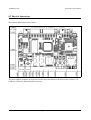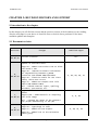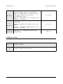
1
OLinuXino-MAXI Open-source single-board Linux computer USER’S MANUAL Revision G, July 2012 Designed by OLIMEX Ltd, 2012 All boards produced by Olimex LTD are ROHS compliant OLIMEX© 2012 OLinuXino User's Manual DISCLAIMER © 2012 Olimex Ltd. Olimex®, logo and combinations thereof, are registered trademarks of Olimex Ltd. Other product names may be trademarks of others and the rights belong to their respective owners. The information in this document is provided in connection with Olimex products. No license, express or implied or otherwise, to any intellectual property right is granted by this document or in connection with the sale of Olimex products. The Hardware project is released under the Creative Commons Attribution-Share Alike 3.0 United States License. You may reproduce it for both your own personal use, and for commertial use. You will have to provide a link to the original creator of the project http://www.olimex.com on any documentation or website. You may also modify the files, but you must then release them as well under the same terms. Credit can be attributed through a link to the creator website: http://www.olimex.com The software is released under GPL. It is possible that the pictures in this manual differ from the latest revision of the board. The product described in this document is subject to continuous development and improvements. All particulars of the product and its use contained in this document are given by OLIMEX in good faith. However all warranties implied or expressed including but not limited to implied warranties of merchantability or fitness for purpose are excluded. This document is intended only to assist the reader in the use of the product. OLIMEX Ltd. shall not be liable for any loss or damage arising from the use of any information in this document or any error or omission in such information or any incorrect use of the product. This evaluation board/kit is intended for use for engineering development, demonstration, or evaluation purposes only and is not considered by OLIMEX to be a finished end-product fit for general consumer use. Persons handling the product must have electronics training and observe good engineering practice standards. As such, the goods being provided are not intended to be complete in terms of required design-, marketing-, and/or manufacturing-related protective considerations, including product safety and environmental measures typically found in end products that incorporate such semiconductor components or circuit boards. Olimex currently deals with a variety of customers for products, and therefore our arrangement with the user is not exclusive. Olimex assumes no liability for applications assistance, customer product design, software performance, or infringement of patents or services described herein. THERE IS NO WARRANTY FOR THE DESIGN MATERIALS AND THE COMPONENTS USED TO CREATE OLINUXINO. THEY ARE CONSIDERED SUITABLE ONLY FOR OLINUXINO. Page 2 of 50 OLIMEX© 2012 OLinuXino User's Manual Table of Contents DISCLAIMER............................................................................................................... CHAPTER 1: OVERVIEW.......................................................................................... 1. Introduction to the chapter.......................................................................................................5 1.1 Features.....................................................................................................................................5 1.2 The OLinuXino family............................................................................................................6 1.2 Target market and purpose of the board..............................................................................6 1.3 Organization.............................................................................................................................7 CHAPTER 2: SETTING UP THE OLINUXINO BOARD....................................... 2. Introduction to the chapter.......................................................................................................8 2.1 Electrostatic warning...............................................................................................................8 2.3 Requirements...........................................................................................................................8 2.4 Powering the board..................................................................................................................9 2.5 Prebuilt software....................................................................................................................10 2.6 Using BitBurner.....................................................................................................................10 2.7 Building the Linux image......................................................................................................12 2.8 How to blink the LED............................................................................................................13 2.8 How setup the I2C, SPI, UART............................................................................................14 CHAPTER 3: OLINUXINO BOARD DESCRIPTION............................................. 3. Introduction to the chapter.....................................................................................................16 3.1 Layout (top view)...................................................................................................................16 CHAPTER 4: THE iMX233 MICROCONTROLLER............................................. 4. Introduction to the chapter.....................................................................................................17 4.1 The microcontroller...............................................................................................................17 CHAPTER 5: CONTROL CIRCUITY....................................................................... 5. Introduction to the chapter.....................................................................................................21 5.1 Reset........................................................................................................................................21 5.2 Clocks......................................................................................................................................21 5.3 Power supply circuit..............................................................................................................21 CHAPTER 6: CONNECTORS AND PINOUT.......................................................... 6. Introduction to the chapter.....................................................................................................24 6.1 Debugging interfaces.............................................................................................................24 6.1.1 UART debug........................................................................................................................25 6.1.2 SJTAG debug......................................................................................................................25 6.1.3 Classic JTAG debug...........................................................................................................26 6.2 SD/MMC slot..........................................................................................................................28 6.3 UEXT module.........................................................................................................................29 Page 3 of 50 OLIMEX© 2012 OLinuXino User's Manual 6.4 GPIO (General Purpose Input/Output) 40pin connector .................................................30 6.5 USB HOSTs............................................................................................................................33 6.6 LAN connector.......................................................................................................................34 6.7 PWR Jack...............................................................................................................................35 6.8 Headphones and line-in connector.......................................................................................35 6.9 Battery connector...................................................................................................................36 6.10 Composite video connector.................................................................................................36 6.11 Boot mode positions.............................................................................................................37 6.12 Jumper description..............................................................................................................38 6.12.1 SCL_SW/SCL_HW and SDA_SW/SDA_HW................................................................38 6.12.2 5V_E...................................................................................................................................39 6.12.3 3.3V_E and 3.3VIO_E jumpers.......................................................................................39 6.12.4 Boot mode selecting jumpers...........................................................................................39 6.13 Additional hardware components......................................................................................39 6.14 Accessories............................................................................................................................40 6.14.1 MOD-SERIAL-USB.........................................................................................................40 CHAPTER 7: BLOCK DIAGRAM AND MEMORY............................................... 7. Introduction to the chapter.....................................................................................................41 7.1 Memory addresses.................................................................................................................41 7.2 Processor block diagram.......................................................................................................42 7.3 Physical memory map...........................................................................................................43 CHAPTER 8: SCHEMATICS...................................................................................... 8. Introduction to the chapter.....................................................................................................44 8.1 Eagle schematic......................................................................................................................44 8.2 Physical dimensions...............................................................................................................46 CHAPTER 9: REVISION HISTORY AND SUPPORT............................................ 9. Introduction to the chapter.....................................................................................................47 9.1 Document revision.................................................................................................................47 9.2 Board revision........................................................................................................................48 9.3 Useful web links and purchase codes...................................................................................49 9.3 Product support.....................................................................................................................50 Page 4 of 50 OLIMEX© 2012 OLinuXino User's Manual CHAPTER 1: OVERVIEW 1. Introduction to the chapter Thank you for choosing the OLinuXino single board computer from Olimex! This document provides a user’s guide for the Olimex OLinuXino board. As an overview, this chapter gives the scope of this document and lists the board’s features. The differences between the members of the OLinuXino family are mentioned. The document’s organization is then detailed. The OLinuXino development board enables code development of applications running on the microcontroller i.MX233, manufactured by FreeScale Semiconductor. OLinuXino is an open-source, open-hardware project and all documentation is available to the customer. 1.1 Features • • iMX233 ARM926J processor at 454Mhz 64 MB RAM • • SD-card connector for booting the Linux image TV PAL/NTSC video output • • 3 USB High Speed Host optional WIFI RTL8188CU module • • Stereo Audio Input Stereo Headphones Audio Output • • two Buttons UEXT connector for connection of different peripherial modules • • 40 pin GPIO for connection of other hardware Board is in shape for fit inside Pactec JM42 plastic box http://www.pactecenclosures.com/pdfs/drw_JM-42.pdf • • Power supply input 6-16VDC PCB dimensions: 3.70'' x 2.15'' (94.0mm x 54.6mm) • Nominal dimensions: 3.70'' x 2.65'' (94.0mm x 67.3mm) Page 5 of 50 OLIMEX© 2012 OLinuXino User's Manual 1.2 The OLinuXino family Table of comparison OLinuXino-MICRO OLinuXino-MINI OLinuXino-MAXI Processor iMX233 @ 454Mhz iMX233 @ 454Mhz iMX233 @ 454Mhz Ram [MB] 64 64 64 # USB hosts 1 3 2 100/150 Mbit Ethernet* No/WIFI option** No/WIFI option*** Yes/WIFI option** GPIO connector 60pins 40pins 40pins # Buttons 3 2 2 Reset button Yes Yes Yes DC power supply 5V 5V-16V 5V-16V Dimensions 3.40'' x 1.70'' 3.70'' x 2.65'' 3.70'' x 2.65'' Breadboarding Yes No No Audio IN connector No Yes Yes Audio OUT connector No Yes Yes UEXT connector Yes Yes No * 100Mbit Ethernet for the wired network of OLinuXino-MAXI. 150Mbit for the WIFI following 811.02n standard. ** All three boards have the option to work with MOD-WIFI_RTL8188, which is USB WIFI modem with RTL8188CU chip and can be purchased separately. MOD-WIFI_RTL8188 can be connected to any of the OLinuXino boards via the USB. *** OLinuXino-MINI has additional option of having RTL8188CU hardware mounted! If you wish RTL8188CU embedded in the device you should purchase OLinuXino-MINI-WIFI. Choosing the embedded WIFI option will leave your USB-HOSTs available for use. 1.2 Target market and purpose of the board The boards from the OLinuXino family are ready to use, easy to setup and are suitable for embedded programming enthusiasts, Linux hobbyists, gadget fans and also professionals (since its low cost makes it very good solution for application orientated embedded systems). The main usage of the board is software embedded development without the urge of understanding perfectly the hardware. Page 6 of 50 OLIMEX© 2012 OLinuXino User's Manual The strong points of the boards are the processor speed, the mobility of the board and the low price. Customers have full access to the technical documentation of the board. The software is released under General Purpose License and the board is considered open-hardware. 1.3 Organization Each section in this document covers a separate topic, organized as follow: – – Chapter 1 is an overview of the board usage and features Chapter 2 provides a guide for quickly setting up the board and software notes – – Chapter 3 contains the general board diagram and layout Chapter 4 describes the component that is the heart of the board: the iMX233 microcontroller – – Chapter 5 is an explanation of the control circuitry associated with the microcontroller to reset. Also shows the clocks on the board Chapter 6 covers the connector pinout, peripherals and jumper description – – Chapter 7 shows the memory map Chapter 8 provides the schematics – Chapter 9 contains the revision history, useful links and support information Page 7 of 50 OLIMEX© 2012 OLinuXino User's Manual CHAPTER 2: SETTING UP THE OLINUXINO BOARD 2. Introduction to the chapter This section helps you set up the OLinuXino development board for the first time. Please consider first the electrostatic warning to avoid damaging the board, then discover the hardware and software required to operate the board. The procedure to power up the board is given, and a description of the default board behavior is detailed. 2.1 Electrostatic warning OLinuXino is shipped in a protective anti-static package. The board must not be exposed to high electrostatic potentials. A grounding strap or similar protective device should be worn when handling the board. Avoid touching the component pins or any other metallic element. 2.3 Requirements In order to set up the OLinuXino optimally, the following items are required: - 6V to 16V source of power with 1A maximum amperage. - SJTAG interface programmer - USB keyboard - Monitor with composite interface or Personal Computer + USB-SERIAL-CABLE - SD card with Linux image Note that the board arrives without SD card or Linux image. You can purchase a card with Linux separately. It is recommended that the user has basic Linux experience. Some of the suggested items can be purchased by Olimex, for instance: iMX233-OLinuXino-SD - SD card with the Linux image USB-SERIAL-CABLE-F - USB serial console cable female (check “6.1.1 UART Debug” for info how to connect it to the board) SY0612E - power supply adapter 12V/0.5A for iMX233-OLinuXino-Maxi Page 8 of 50 OLIMEX© 2012 OLinuXino User's Manual 2.4 Powering the board The board is powered either via the PWR jack or via a battery. It should be supplied from a 6V to 16V source with maximum current of 1A from the power jack. All measures below are taken at 10V. If measuring the current consumption it should be around 0.06A before initializing all the peripherals. The consumption raises to 0.12A without LAN and USB hosts initialized and Linux running. The consumption goes up 0.15A with the Linux running when LAN and both USB hosts initialized. If you have a standard USB flash drive attached to a USB host, Linux and LAN running the typical consumption is around 0.20A. When powered by the typical 3.7V battery the LAN and USB-hosts will be powered-off if you use the external 3.3V DC-DC (they will stil work if using the internal in the processor DC-DC). The consumption from the battery when Linux is running is around 0.75A. IMPORTANT! We discovered a situation which might leave some of the SD cards (iMX233OLinuXino-SD) in unrecoverable state when powering OLinuXino-MICRO. The problem might occur if two specific conditions are met simultaneously: 1)Plugged iMX233-OLinuXino-SD micro SD card with holographic sticker on its back side (some of the cards we have distributed are from a brand that places holographic sticker on their backs, the other half lack such a sticker) 2)Plugged USB-SERIAL-CABLE-F at the moment when powering the board If you happen to have received SD card with holographic sticker on its back side and you use it with OLinuXino-MICRO and you plug USB-SERIAL-CABLE and then you power the board there is a chance of malfunction of the SD card. There are two possible workarounds to protect the SD card. The first one is simpler and the second one requires some soldering experience. Workaround 1: First insert the iMX233-OLinuXino-SD card and then power the board (and if powering the board from a battery also press the PWR button). Wait 4-5 seconds and then connect the USB-SERIAL-CABLE-F. After the initial power-up it is safe to use the reset button. Workaround 2: You will need a Shottky diode. The Shottky should be soldered on the USBPage 9 of 50 OLIMEX© 2012 OLinuXino User's Manual SERIAL-CABLE-F TX line/wire (RED cable) with anode towards the board. When you power the board by battery you have to press the PWR_BUT to start the board. If you start Linux and it is already running no matter which powering method you use (PWR_JACK or BAT) pressing the PWR_BUT will put the Linux in power-save mode. When you power the board by battery you have to press the PWR_BUT to start the board. If you start Linux and it is already running no matter which powering method you use (PWR_JACK or BAT) pressing the PWR_BUT will put the Linux in power-save mode. For the European customers we sell a power supply adapter 12V/0.5A - SY0612E. 2.5 Prebuilt software Note that the boards arrive without Linux or SD card. The Linux image can be purchased separately on a SD card or you can built and adjust it yourself. When we program the boards we change the default position of the following HW_OCOTP_ROM0 fuses of the processor: SD_MBR_BOOT(3) - Blown SD_POWER_GATE_GPIO(21:20) – 10-PWM3 For burning the fuse position we use the BitBurner software. This operation is discussed in details before. Proceed with great caution when burning fuses since it is irreversible operation. 2.6 Using BitBurner IMPORTANT! MODIFYING THE FUSES IS IRREVERSIBLE PROCESS! BURNING THE WRONG FUSES MIGHT DAMAGE OLINUXINO IRREVERSIBLY! BURNING WRONG FUSES MIGHT CAUSE BOOT PROBLEMS! BURN FUSES AT OWN RISK! The bit burning is done via the USB of the computer connected to the OLINUXINO board and the BitBurner software. To be able to burn the fuses you will need to make a custom cable that connects a USB with the 3 pin holes found at the bottom of the board named “GND”, “DP”, “DM” (check the picture below for a better view how the three wires must be connected. Page 10 of 50 OLIMEX© 2012 OLinuXino User's Manual After soldering the three wires you can place a marker on each of them or use colored wires to be able to distinguish them. You can also use some gel to keep them tight on the USB connector. On the opposite side of the cables you might place 50mil (1.27mm) male connector following the order of the signals. Please also restrain from using wires longer than 20 cm since that might make the connection unreliable. Download BitBurner from https://www.olimex.com/dev/OLINUXINO/iMX233OLINUXINO/BitBurner.v1.0.4.6.zip. Extract it and start the .exe. If you connect everything you should see and choose HID-compilant device from the “Select device” drop-down menu. Page 11 of 50 OLIMEX© 2012 OLinuXino User's Manual 2.7 Building the Linux image Note that building the Linux image from scratch is a time-consuming task. Even with powerful machine and fast internet connection it might take few hours compiling. Some Linux distributions might lack the tools required to compile/build/execute scripts/download from repository – how to get those is not discussed below. The Linux image is created and downloaded from https://github.com/Freescale/fsl-community-bspplatform. For the test here we used Debian 6.0 with GNOME visual libraries. The steps we did: 1) From the terminal created folder “bin” in home folder: user@dist$: mkdir bin user@dist$: cd bin Add bin directory to PATH in order to do the next steps easier. Else navigate to the right folders. 2) Installed `repo` utility needed for the bitbake file fetching from the repository: user@dist$: curl https://dl-ssl.google.com/dl/googlesource/git-repo/repo > ~/bin/repo user@dist$: chmod a+x ~/bin/repo 3) Created directory for the project and download the BSP source from the git repository: user@dist$: mkdir fsl-community-bsp user@dist$: cd fsl-community-bsp ~/fsl-community-bsp$: repo init -u https://github.com/Freescale/fsl-community-bsp-platform -b denzil ~/fsl-community-bsp$: repo sync 4) You can change the settings for the build if you want at fsl-community-bsp/build/conf/local.conf. I changed the “machine” name to “imx233-olinuxino-maxi”. For Linux kernel configurations and settings you can do (of course you can use also the default settings): ~/fsl-community-bsp$:. ./setup-environment build ~/fsl-community-bsp/build$:bitbake linux-imx -c menuconfig Check the image below: Page 12 of 50 OLIMEX© 2012 OLinuXino User's Manual 5) Now to start building the image: ~fsl-community-bsp$:. ./setup-environment build ~fsl-community-bsp/build $: bitbake core-image-minimal Note: on different Linux distributions you might have different tools installed and you will probably need to install dependencies needed for the compile/build scripts. Here are some (but not all) of the mandatory ones: G++; diffstat; texi2html; chrpath; gawk; texinfo; some git client. To ensure you have the latest version supported with all the updates visit https://github.com/OLIMEX/OLINUXINO and https://github.com/Freescale/fsl-community-bspplatform. 2.8 How to blink the LED In this sub-chapter you will find a way to achieve the most basic task in electronics – the “Hello World” of electronics - blinking the LED. First we set the pin responsible for the LED as an output and we can set its value manually to high or low position – make it blink manually. The LED mounted on the board uses GPIO65. You can use external diode instead of the one mounted - you have to look at the table “The Linux implementation of pins” in the hardware section to get the correct linux name for the GPIO pin. Page 13 of 50 OLIMEX© 2012 OLinuXino User's Manual echo out > /sys/class/gpio/gpio65/direction echo 1 > /sys/class/gpio/gpio65/value If you want to set the blink off you should change the value on the second line to: echo 0 > /sys/class/gpio/gpio65/value To show the info for all GPIOs: ls /sys/class/gpio To make it turn on – turn off automatically (e.g. blink) we use the text redactor VI to write the Linux script: echo out > /sys/class/gpio/gpio65/direction while true do echo 1 > /sys/class/gpio/gpio65/value sleep 1 echo 0 > /sys/class/gpio/gpio65/value sleep 1 done We save it as as “gpio” and we make it executable with chmod +x gpio then we execut the script with: ./gpio The LED should start blinking with 0.5Hz. 2.8 How setup the I2C, SPI, UART Good place to check if you are trying to configure the I2C, SPI, UART etc via Linux is http://www.inf.furb.br/~maw/asm51/Telit_GE863-PRO3_Linux_SW_UserGuide_r5.pdf. Telit have explained how to do it with their board but it follows the same pattern for OLinuXino. Another way to test I2C is using the i2c-tools utility (), which is available in OpenEmbedded. For SPI you can use spidev tool: Page 14 of 50 OLIMEX© 2012 OLinuXino User's Manual Git link(click) , check the spidev_test.c code for an example. Page 15 of 50 OLIMEX© 2012 OLinuXino User's Manual CHAPTER 3: OLINUXINO BOARD DESCRIPTION 3. Introduction to the chapter Here you get acquainted with the main parts of the board. Note the names used on the board might differ from the names used below to describe them. For the actual names check the OLinuXino board itself. 3.1 Layout (top view) Page 16 of 50 OLIMEX© 2012 OLinuXino User's Manual CHAPTER 4: THE iMX233 MICROCONTROLLER 4. Introduction to the chapter In this chapter is located the information about the heart of OLinuXino – its microcontroller. The information is a modified version of the datasheet provided by its manufacturers. 4.1 The microcontroller ARM926 CPU Running at 454 MHz Integrated ARM926EJ-S CP 16-Kbyte data cache and 16-Kbyte instruction cache — One-wire JTAG interface — Resistor-less boot mode selection using integrated OTP values 32Kbytes of Integrated Low-Power On-Chip RAM 64 Kbytes of Integrated Mask-Programmable On-Chip ROM 1 Kbit of On-Chip One-Time-Programmable (OCOTP) ROM Universal Serial Bus (USB) High-Speed (Up to 480 Mb/s), Full-Speed (Up to 12 Mb/s) — Full-speed/high-speed USB device and host functions — Fully integrated full-speed/high-speed Physical Layer Protocol (PHY) — Mass storage host-capable (uncertified by USB-IF) Power Management Unit — Single inductor DC-DC switched converter with multi-channel output supporting Li-Ion batteries. — Features multi-channel outputs for VDDIO (3.3 V), VDDD (1.2 V), VDDA (1.8 V), VDDM (2.5V) and regulated 4.2V source. — Direct power from 5-V source (USB, wall power, or other source), with programmable current limits for load and battery charge circuits. — Silicon speed and temperature sensors enable adaptive power management over temperature and silicon process. Audio Codec — Stereo headphone DAC with 99 dB SNR — Stereo ADC with 85 dB SNR — Stereo headphone amplifier with short-circuit protection and direct drive to eliminate bulky capacitors — Amplifiers are designed for click/pop free operation. Page 17 of 50 OLIMEX© 2012 OLinuXino User's Manual — Two stereo line inputs — Microphone input — SPDIF digital out 16-Channel Low-Resolution ADC — 6 independent channels and 10 dedicated channels — Resistive touchscreen controller — Temperature sensor controller — Absolute accuracy of 1.3% — Up to 0.5% with bandgap calibration Security Features — Read-only unique ID for digital rights management algorithms — Secure boot using 128-bit AES hardware decryption — SHA-1 hashing hardware — Customer-programmed (OTP) 128 bit AES key is never visible to software. External Memory Interface (EMI) — Provides memory-mapped (load/store) access to external memories — Supports the following types DRAM: – 1.8V Mobile DDR – Standard 2.5V DDR1 Wide Assortment of External Media Interfaces — Up to four NAND flash memories with hardware management of device interleaving — High-speed MMC, secure digital (SD) — Hardware Reed-Solomon Error Correction Code (ECC) engine offers industry-leading protection and performance for NANDs. — Hardware BCH ECC engine allowing for up to 20-bit correction and programmable redundant area. Dual Peripheral Bus Bridges with 18 DMA Channels — Multiple peripheral clock domains save power while optimizing performance. — Direct Memory Access (DMA) with sophisticated linked DMA command architecture saves power and off-loads the CPU. Highly Flexible Display Controller — Up to 24-bit RGB (DOTCK) modes — Up to 24-bit system-mode including VSYNC and WSYNC modes. — Up to VGA (640x480) resolution at 60Hz LCD panel support — 8-bit data ITU-R BT.656 D1 digital video stream output mode (PAL/NTSC), with onthefly RGB to YCbCr color-space-conversion. — Flexible input formats Pixel Processing Pipeline (PXP) Page 18 of 50 OLIMEX© 2012 OLinuXino User's Manual — Provides full path from color-space conversion, scaling, alpha-blending to rotation without intermediate memory access — Bi-linear scaling algorithm with cropping and letterboxing — Alpha-blend, BITBLT, color-keying — Memory efficient block-based rotation engine — Supports up to eight overlays Integrated TV-Out Support — Integrated PAL/NTSC TV-encoder fully pipelined to display controller’s D1 resolution output stream — Integrated low-power 10-bit Video DAC (VDAC) for composite analog video output. Data Co-Processor (DCP) — AES 128-bit encryption/decryption — SHA-1 hashing — High-speed memory copy Three Universal Asynchronous Receiver-Transmitters (UARTs) — Two high-speed application UARTs operating up to 3.25 Mb/s with hardware flow control and dual DMA. — Debug UART operates at up to 115Kb/s using programmed I/O. I2C Master/Slave — DMA control of an entire EEPROM or other device read/write transaction without CPU intervention Dual Synchronous Serial Ports (for SPI, MMC, SDIO, Triflash) — Up to 52MHz external SSP clock for all modes, including SPI — 1-bit, 4-bit and 8-bit MMC/SD/SDIO modes — Compliant with SDIO Rev. 2.0 — SPI with single, dual and quad modes. Four-Channel 16-Bit Timer with Rotary Decoder Five-Channel Pulse Width Modulator (PWM) Real-Time Clock — Alarm clock can turn the system on. — Uses the existing 24-MHz XTAL for low cost or optional low power crystal (32.768 kHz or 32.0 kHz), customer-selectable via OTP. SPDIF Transmitter Dual Serial Audio Interface (SAIF), Three Stereo Pairs — Full-duplex stereo transmit and stereo receive operations — Cell phone baseband processor connection and external ADCs and DACs — Bluetooth hands-free connection — Analog I/O for peripheral bus breakouts Page 19 of 50 OLIMEX© 2012 OLinuXino User's Manual — I2S, left-justified, right-justified, and non-standard formats Customer-Programmable One-Time-Programmable (OTP) ROM via Integrated eFuse Block — Resistor-less boot mode selection — 128-bit boot mode crypto key — Boot mode specification of NAND characteristics for device that the customer is soldering to the board. This means no more costly delays waiting for new device support in t he boot ROM. — Fully software-programmable and accessible Flexible I/O Pins — All digital pins have drive-strength controls — Most non-EMI digital pins have general-purpose input/output (GPIO) mode. For comprehensive information on the microcontroller visit the Freescale’s web page for a datasheet. At the moment of writing the microcontroller datasheet can be found at the following link: http://www.freescale.com/files/dsp/doc/ref_manual/IMX23RM.pdf Page 20 of 50 OLIMEX© 2012 OLinuXino User's Manual CHAPTER 5: CONTROL CIRCUITY 5. Introduction to the chapter Here you can find information about reset circuit and quartz crystals locations, the power supply circuit is discussed. 5.1 Reset OLinuXino's reset circuit includes R9 (47KΩ), R10 (47 Ω), T1, T2, Q1 and a RESET button. The RESET is specific for the fact that it is accomplished when the quartz is disconnected using 3.3V and the transistors T1 and T2. 5.2 Clocks 24 MHz quartz crystal Q1 is connected to pins 121 and 122 of the iMX233 processor. 25 MHz quartz crystal Q2 is found at pins 60 and 61 of the Ethernet controller – LAN9512-JZX. 5.3 Power supply circuit The power supply circuit of OLinuXino-MAXI allows flexible input supply from 6V to 16V direct current. This means a wide range of power supplies, adapters, converters are applicable. The maximum amperage recommended is 1A by default (0.250mA if 3.3VIO_E is closed – read below). All measures below are taken at 10V external supply. Page 21 of 50 OLIMEX© 2012 OLinuXino User's Manual If measuring the current consumption it should be around 0.06A before initializing all the peripherals. The consumption raises to 0.12A without LAN and USB hosts initialized and Linux running. The consumption goes up 0.15A with the Linux running when LAN and both USB hosts initialized. If you have a standard USB flash drive attached to a USB host, Linux and LAN running the typical consumption is around 0.20A. When powered by the typical 3.7V battery the LAN and USB-hosts are disabled. The consumption when Linux is running is around 0.75A. The board can be powered either from the power jack or from the LIPO_BAT connector. Note that since standard batteries can't provide the voltage needed for the board it is advisable to use the power from the power jack. When you use the LIPO_BAT connector and a battery the chip handling the Ethernet and the USB hosts is disabled. Also the power button has alternative function when the board is powered by a battery – check 6.13. If you have successfully powered the board the red PWR LED will turn on. Note that it is possible to have the PWR LED on even if there isn't enough power for proper operation of the board and all the peripherals currently connected. Page 22 of 50 OLIMEX© 2012 OLinuXino User's Manual The jumper 5V_E (5V Enable) which is closed by default enables powering the board via the power supply circuit. The 3.3V_E (3.3V Enable) jumper when closed enables the 3.3V power line. Note the 3.3VIO_E jumper which by default is closed – if you open it (cut it) - it disables the U6 DC-DC converter and enables a built-in the iMX233 DC-DC. The problem is that the built-in DCDC has a limit of 250mA of amperage the chip heats a bit so we decided to put external DC-DC for better stability. When working with 3.3VIO_E closed pay attention to the amperage used. If 3.3VIO_E is closed(soldered) – it enables the additional DC-DC which is the better solution if powering the board from external supply. However, if 3.3VIO_E is closed and you power the board from a battery the LAN and the USB-HOSTs will not receive enough power and will be disabled. Page 23 of 50 OLIMEX© 2012 OLinuXino User's Manual CHAPTER 6: CONNECTORS AND PINOUT 6. Introduction to the chapter In this chapter are presented the connectors that can be found on the board all together with their pinout and notes about them. Jumpers functions are described. Notes and info on specific peripherals are presented. Notes regarding the interfaces are given. 6.1 Debugging interfaces If you don't have a separate monitor or display around, and you don't wish to swap cables constantly with your personal computer using the debug interfaces provide better option for you OLinuXino experience. There are three debugging options available on the OLinuXino. It is preferable to use one of the first two - UART or SJTAG but in case you want to use the classic 6-wire parallel JTAG there is an option explained below. Page 24 of 50 OLIMEX© 2012 OLinuXino User's Manual 6.1.1 UART debug The first one is a debug UART interface – U_DEBUG. You can use our USB-SERIAL-CABLE for debugging via the UART. In order to avoid SD card malfunction, when using the USB-SERIAL-CABLE-F with OLinuXino-MAXI it is advisable to first insert the iMX233-OLinuXino-SD card and then power the board (if using battery also press the PWR button). Wait 4-5 seconds and then connect the USB-SERIAL-CABLE-F. Please also check “2.4 Powering the board” for detailed info. Note on how to use the U_DEBUG with USB-SERIAL-CABLE-F which has RED GREEN BLUE wires GND=BLUE, RX(INPUT)=GREEN, TX(OUTPUT)=RED. You have to connect to OLinuXino-MAXI U_DEBUG connector in this sequence: BLUE wire to pin.3 (GND) GREEN wire to pin.2 (TX) RED wire to pin.1 (RX) U_DEBUG Pin # Signal Name Processor Pin # 1 PWM0/DUART_RXD 125 2 PWM1/DUART_TXD 126 3 GND 30, 35, 98, 105, 112, 118 4 DEBUG 84 You can also check the pin names at the bottom of the board under the U_DEBUG header. 6.1.2 SJTAG debug The second interface is the Serial JTAG (SJTAG) one-wire interface. It works with various external JTAG debugger dongles through a Freescale-defined FPGA/CPLD. SJTAG supports the Green Hills Slingshot and ETM probe debugger dongles, as well as those made by ARM, Abatron, and Lauterbach. Page 25 of 50 OLIMEX© 2012 OLinuXino User's Manual Note that the SJTAG interface comes without plastic header mounted. The HW_DIGCTL_CTRL_USE_SERIAL_JTAG bit in the digital control block selects whether the one-wire serial JTAG interface or the alternative six-wire parallel JTAG interface is used. There are other options in the digital control block which might interest you and our advice is to check the iMX233's datasheet released by Freescale. SJTAG Pin # Signal Name Processor Pin # 1 3.3VREG - 2 GND 30, 35, 98, 105, 112, 118 3 SJTAG_PSW 119 4 DEBUG 84 The pin names are also written at the bottom of the board for your convenience. 6.1.3 Classic JTAG debug The third option is to use the classic 6-pin parallel JTAG (not including GND and VCC). There are pads left for this option at the bottom of the board under the SD card holder. They are named individually and framed near a “JTAG” name. The important thing is that these pins are multiplexed with the SD card signals. In order to use the 6-pin JTAG you will have to stop using the SD card. Note also that the classic JTAG interface comes without plastic header mounted so in order to use it you will need to use wires for connection. Consider the the software settings required to switch from SJTAG to 6-pin JTAG and vice verse referring to the iMX233 manual. For instance: The HW_DIGCTL_CTRL_USE_SERIAL_JTAG bit in the digital control block selects whether the serial JTAG interface or the alternative six-wire parallel JTAG interface is used. HW_DIGCTL_CTRL_USE_SERIAL_JTAG - 0x0 - Selects whether the one-wire serial JTAG interface or the alternative six-wire parallel JTAG interface is used. 0 = Parallel six-wire JTAG is Page 26 of 50 OLIMEX© 2012 OLinuXino User's Manual enabled and is mapped to a collection of module pins that must be enabled by programming their MUXSEL bits in the pin control block. 1 = Serial JTAG is enabled and uses the dedicated DEBUG pin. The ROM bootcode writes this field prior to enabling JTAG, selecting which type of JTAG pin signaling to use. OLD_JTAG = 0x0 Use six-wire parallel JTAG mode. SERIAL_JTAG = 0x1 Use one-wire serial JTAG mode. It is good idea to check the datasheet of the iMX233 processor for all the options in the digital control block. The processor's datasheet should be always the first piece of paper you consult when dealing with electronics. Classic JTAG (multiplexed with SD card) Pin # Signal Name Processor Pin # 1 SSP1_DATA1 85 2 SSP1_DATA0 84 3 GND 30, 35, 98, 105, 112, 118 4 SSP1_SCK 90 5 SD_VCC - 6 SSP1_CMD 83 7 SSP1_DATA3 87 8 SSP1_DATA2 86 Notice that the pad numeration is written at the bottom of OLinuXino-MAXI under the microSD card connector. Please check the manual part for microSD card for a schematic of the pins. Page 27 of 50 OLIMEX© 2012 OLinuXino User's Manual 6.2 SD/MMC slot The microSD card slot is a standard 8pin connector. We have tested a number of microSD cards on the OLinuXino boards and all of them worked fine regardless manufacturer or capacity. However, keep in mind that some of the lower quality microSD cards might draw too much current from the slot which might cause power-state problems. If you suspect the microSD card is causing problems please try using another one of better quality for better results. microSD card connector Pin # Signal Name Processor Pin # 1 SSP1_DATA2 86 2 SSP1_DATA3 87 3 SSP1_CMD 83 4 SD_VCC - 5 SSP1_SCK 90 6 GND 30, 35, 98, 105, 112, 118 7 SSP1_DATA0 84 8 SSP1_DATA1 85 Notice that the pad numeration is written at the bottom of OLinuXino-MAXI under the microSD Page 28 of 50 OLIMEX© 2012 OLinuXino User's Manual card connector. When removing the card, please make sure that you release it from the connector by pushing and NOT by pulling the card directly (this can damage both the connector and the microSD card). 6.3 UEXT module OLinuXino board has UEXT connector and can interface Olimex's UEXT modules. For more information on UEXT please visit: http://www.olimex.com/dev/OTHER/UEXT.pdf *Note the two jumpers PIN29/SOFT_CL – PIN22/LCD_EN/I2C_SCL, and PIN28/SOFT_SDA3 – PIN21/LCD_HSYNC/I2C_SDA which by default are set to a software SPI. They can be used to set the whole UEXT to a hardware SPI. Page 29 of 50 OLIMEX© 2012 OLinuXino User's Manual UEXT connector Pin # Signal Name Processor Pin # 1 +3.3VREG - 2 GND 30, 35, 98, 105, 112, 118 3 AUART1_TXD 127 4 AUART1_RXD 128 5 I2C_SCL 34(default) OR 11* 6 I2C_SDA 31(default) OR 15* 7 PIN9/LCD_D08/SSP2_MISO 22 8 SSP2_MOSI 21 9 SSP2_SCK 33 PIN12/LCD_D11/UEXT_CS 25 10 The UEXT pinout is also printed at the bottom of the board under the connector. 6.4 GPIO (General Purpose Input/Output) 40pin connector The GPIO pins are led out on a separate 40pin connecter. They allow the user to attach additional hardware, check readings or perform hardware debug. The “GPIO Pin#” column shows connector number and does NOT represent the naming on the bottom of the board. Page 30 of 50 OLIMEX© 2012 OLinuXino User's Manual GPIO connector hardware GPIO Signal Name Pin# Processor pin# GPIO Pin# Signal Name Processor pin# 1 BAT 103 21 PIN8/LCD_D07 9 2 GND 30, 35, 98, 105, 112, 118 22 PIN27/PWM2 91 3 PIN17/LCD_D16 19 23 PIN7/LCD_D06 8 4 PIN18/LCD_D17/LAN_RES 20 24 PIN28/SOFT_SDA 31 5 PIN16/LCD_D15 28 25 PIN6/LCD_D05 7 6 PIN19/LCD_DOTCLK 17 26 PIN29/SOFT_SCL 34 7 PIN15/LCD_D14 29 27 PIN5/LCD_D04 6 8 PIN20/LCD_VSYNC 16 28 PIN30 81 9 PIN14/LCD_D13 26 29 PIN4/LCD_D03 5 10 PIN21/LCD_HSYNC/ I2C_SDA 15 30 PIN31 82 GPIO Name Pin# Processor pin# GPIO Name Pin# Processor pin# 11 PIN13/LCD_D12 27 31 PIN3/LCD_D02 4 12 PIN22/LCD_EN/I2C_SCL 11 32 PIN32/LRADC1 107 13 PIN12/LCD_D11/UEXT_CS 25 33 PIN2/LCD_D01 3 14 PIN23/LCD_DISP 12 34 PIN33/LRADC0 108 15 PIN11/LCD_D10 24 35 PIN1/LCD_D00 2 16 PIN24/LCD_WR 13 36 PIN34/MIC 116 17 PIN10/LCD_D09 23 37 +5VUEXT 102 18 PIN25/LCD_RS 14 38 3.3VREG - 19 PIN9/LCD_D08/ SSP2_MISO 22 39 VIN - 20 PIN26/LCD_CS 10 40 GND 30, 35, 98, 105, 112, 118 The hardware is associated differently in the Linux following the GPIO naming conventions suggested in the iMX233 datasheet. You can check the connection between Linux naming of the pin, Olimex naming of the pin and the consecutive connector pin number in the table below. The Page 31 of 50 OLIMEX© 2012 OLinuXino User's Manual ones filled with “Not implemented” doesn't have Linux support by the time of writing and will be updated overtime. “Linux GPIO” is the one you should use in Linux (the one in the datasheet); “OLinuXino name” is the pin as written on the bottom of the board. ”OLinuXino GPIO Connector #” is the consecutive number of pins with BAT being Pin#1 and GND#40. Note that if “OLinuXino Name” starts with P and then is followed by a number X, the PX is the name written on the bottom of the board (under the connector) with white ink. If “OLinuXino Name” is other text it is a signal used for the hardware of the board but still can be controller by the Linux (it can't be found at the GPIO connector though). The Linux implementation of pins Linux GPIO/iMX OLinuXino Name 233 GPIO OLinuXino GPIO Connector # Linux GPIO/iMX 233 GPIO OLinuXino Name OLinuXino GPIO Connector # 0 PIN9 19 32 to 39 Not implemented Not implemented 1 PIN10 17 51 PIN25 18 2 PIN11 15 52 PIN24 16 3 PIN12 13 53 PIN26 20 4 PIN13 11 55 PIN22 12 5 PIN14 9 56 PIN21 10 6 PIN15 7 64 JTAG_TDO1 SSP1_CMD Not implemented 7 PIN16 5 65 LED1 Not implemented 16 PIN17 3 91 PIN30 28 17 PIN18 4 92 PIN31 30 19 TEST_PAD Not implemented 20 UEXT_SPI2_MOSI 9 23 PIN29 26 24 UEXT_SPI2_SCK Not implemented 25 PIN28 24 30 UEXT_TX1 Not implemented 31 UEXT_RX1 Not implemented Page 32 of 50 OLIMEX© 2012 OLinuXino User's Manual Below you can find the GPIO_CON as seen in the schematic: When looking at the bottom of OLinuXino-MAXI near the GPIO connector there is also an additional GND pad named GND_PIN which is a fast way to have access to a ground signal. 6.5 USB HOSTs The USB hosts and the Ethernet are controller by a single chip (LAN9512) which handles both functionality. The LAN9512 contains a Hi-Speed USB 2.0 hub with two fully-integrated downstream USB 2.0 PHYs, an integrated upstream USB 2.0 PHY, a 10/100 Ethernet MAC/PHY controller, and an EEPROM controller. It offers SMSC's highest level of USB 2.0 and 10/100 Ethernet compliance and interoperability. Additionally, the LAN9512 devices simplify system design by leveraging the existing USB stack and reducing the PCB footprint by up to 65% compared to discrete competitive solutions. USB-based networking technology offers a cost-effective and smart design alternative to traditional PCI/PCI-Express networking solutions due to the flexibility of routing and placement of Ethernet and USB connectivity ports. The big advantage of having USB hosts available over USB devices is that you can use them to power devices. Page 33 of 50 OLIMEX© 2012 OLinuXino User's Manual The signals follow the familiar and standard USB host pattern: USB 2-level host PIN# SIGNAL NAME 1 USB_PWR_A 2 USB_HOST_D- 3 USB_HOST_D+ 4 GND 6.6 LAN connector The Ethernet connectivity is handled by the LAN9512 controller (which also incorporates a USB module in it). The signals found on the Ethernet connector are listed in the table below: LAN connector PIN# SIGNAL NAME 1 TX+ 2 TX- 3 VDD 4 NOT CONNECTED 5 NOT CONNECTED 6 VDD 7 RX+ 8 RX- The two leds on the front side of the LAN connector show the state of the Ethernet. The meaning behind the different states can be found in the table below: Page 34 of 50 OLIMEX© 2012 OLinuXino User's Manual LED Color Usage Right Green Link status Left Yellow Activity status 6.7 PWR Jack The power jack used is the typical 2.5mm one used by Olimex in most of our products. You should provide between 6 and 16 volts @ 1A to the board. Pin # Signal Name 1 Power Input 2 GND More info about the power supply can be found in chapter 5 of this manual 6.8 Headphones and line-in connector Standard audio jack and phone jack are mounted for the audio interfacing. Headphones/Audio out connector Pin# SIGNAL NAME Processor Pin# 2 L channel 113 3 R channel 109 5 GND GND pins The headphones resistance is 16 Ohms! Page 35 of 50 OLIMEX© 2012 OLinuXino User's Manual 6.9 Battery connector When using the battery connector keep in mind that it is an energy solution that wouldn't be able to power the board and all the peripherals. The voltage of a 3.7V LIPO battery would be enough to power the processor and the memory but won't be enough to power the LAN and the USB hosts. Pin # Signal Name 1 VBAT 2 GND The pins are also written on the top of the board in the base of the connector. 6.10 Composite video connector The composite video is the connector you should use if you wish OLinuXinoMAXI video output on a monitor. The whole signal is controlled by pin #104 from the i.MX233 processor. The + signal is lead to the middle of the connector. The outside part is the GND. Page 36 of 50 OLIMEX© 2012 OLinuXino User's Manual 6.11 Boot mode positions The iMX233 can boot the operating system from different locations. The default location for the Linux files we used is the microSD card. There are 4(four) jumpers responsible for the boot location: D03, D02, D01 and D00. They are located on the top of the board between the processor and 40pin GPIO connector. Note that the jumpers are SMD type and opening a jumper would require cutting, closing a jumper would require soldering. To be able to do the quoted operations you will need basic engineering skills and experience. You can check below the table or the schematic for the correct positions. Value of “1” means the jumper is closed. BOOT MODE D03 d02 d01 d00 USB 0 0 0 0 3.3V I2C Master 0 0 0 1 33.3V SPI Flash 1 Master 0 0 1 0 3.3V SPI Flash 2 Master 0 0 1 1 3.3V NAND 0 1 0 0 Start up waits for JTAG debugger connection 0 1 1 0 3.3V SD/MMC 1 (Default !!!) 1 0 0 1 3.3V SD/MMC 2 1 0 1 0 Page 37 of 50 OLIMEX© 2012 OLinuXino User's Manual 6.12 Jumper description Please note that all the jumpers on the board are SMD type. If you feel insecure of your soldering/cutting technique it is better not to try to adjust the jumpers. 6.12.1 SCL_SW/SCL_HW and SDA_SW/SDA_HW Those two jumpers must be moved together – there are two available options – configuring software I2C interface (SCL_SW, SDA_SW) or hardware I2C interface (SCL_HW, SDA_HW positions). The default position is SCL_SW/SDA_SW Page 38 of 50 OLIMEX© 2012 OLinuXino User's Manual 6.12.2 5V_E The 5V_E jumper allows control over the powering line. If you want to disable the 5V powering line open 5V_E jumper. The default position is closed. 6.12.3 3.3V_E and 3.3VIO_E jumpers Important these jumpers must be moved together! Closing both of 3.3V_E and 3.3VIO_E at the same time will damage the processor. One of them has to be open (unsoldered/cut). There are two possible positions: 1) 3.3V_E closed (soldered), 3.3VIO_E open (unsoldered/cut) 2) 3.3V_E open (unsoldered/cut), 3.3VIO_E closed (soldered) In the default variant 1) the board uses the mounted by OLIMEX DC-DC 3.3V convertor which when the board is powered by external supply is the better alternative. However, if you use battery it will not power the chip handling the USB and the LAN functionality. Basically the board will lack USB-HOSTs and LAN when jumpers are set in variant 1) and the board is powered by a battery via the BAT connector. If you set the jumpers in 2) state the board's 3.3V will be handled by the built-in iMX233 DC-DC but the problem is it isn't configured to be used with another chip so it doesn't provide enough current for all the USB-HOSTs and the LAN which might cause some of the devices plugged in the USB to lack power and also might burn the chip if too much current is drawn. However, in this 2) mode of jumpers it is possible to power the board from a battery and still have some current on the USB-HOSTs and the LAN. The maximum current the built-in DC-DC can provide safely is 200mA. 6.12.4 Boot mode selecting jumpers The boot mode is discussed in chapter 6.11 of this manual. 6.13 Additional hardware components The components below are mounted on OLinuXino but are not discussed above. They are listed here for completeness: Reset button - used to reset the board Page 39 of 50 OLIMEX© 2012 OLinuXino User's Manual Power button – when Linux is running pressing PWR_BUT will put the board in low power mode; when powered by battery PWR_BUT is used to initially power up the board – and pressing the board again after it is powered will put it low power mode Recovery pads (REC) - these can be used for attaching a recovery button; when powered by battery the recovery button is used to bring the processor to normal power mode – you can shortcircuit the pads for this feature without having to mount a button 512 (32M x 16) MBit DDR SDRAM - the exact memory used in the first revisions of the board is Xylinx HY5DU121622D LED1 + Power LED 6.14 Accessories Here you will find additional information for Olimex products you can use with OLinuXino-MAXI purchase 6.14.1 MOD-SERIAL-USB The cable for the U_DEBUG interface that can be purchased for additional cost has three cables It is important to specify in your purchase order whether you want the MOD-SERIAL-USB variant with male of female connectors. Page 40 of 50 OLIMEX© 2012 OLinuXino User's Manual CHAPTER 7: BLOCK DIAGRAM AND MEMORY 7. Introduction to the chapter On the next page you can find a memory map for this family of processors. It is strongly recommended to refer to the original datasheet released by Freescale for one of higher quality. 7.1 Memory addresses Below is the table with some of the most frequently used addresses. For full list of addresses check the manual released by Freescale (Chapter Memory Map). Decode Device block Mnemonic Start address End address Size AHB On-chip RAM OCRAM 0x00000000 0x00007FFF 32KB On-chip RAM alias OCRAM 0x00008000 0x3FFFFFFF External memory 0x40000000 0x5FFFFFFF 512MB Default Slave 0x60000000 0x7FFFFFFF 512M Page 41 of 50 OLIMEX© 2012 OLinuXino User's Manual 7.2 Processor block diagram Page 42 of 50 OLIMEX© 2012 OLinuXino User's Manual 7.3 Physical memory map Page 43 of 50 OLIMEX© 2012 OLinuXino User's Manual CHAPTER 8: SCHEMATICS 8. Introduction to the chapter In this chapter are located the schematics describing logically and physically OLinuXino. 8.1 Eagle schematic OLinuXino schematic is visible for reference here. You can also find them on the web page for OLinuXino at our site: http://www.olimex.com/dev/imx233-OLinuXino-maxi.html. They are located in HARDWARE section. The EAGLE schematic is situated on the next page for quicker reference. Page 44 of 50 OLIMEX© 2012 OLinuXino User's Manual U1 Q1 Q24.000M Hz/HC-49SM/SMD/20ppm/20pF C26 1uF 112 118 105 117 USB_DP USB_DM VSSA1 VSSA2 VSSA4 VAG 124 USB_DP 123 USB_DM 113 HPL 109 HPR 111 HP_VGND LCD_CS LCD_RS LCD_WR LCD_RESET/GPMI_CE3N LCD_ENABLE/I2C_SCL LCD_HSYNC/I2C_SDA LCD_VSYNC/LCD_BUSY LCD_DOTCK/GPMI_RDY3 115 LINE1_INL 114 LINE1_INR LED/GREEN/3MM LED1 PIN34/MIC 116 MIC PIN33/LRADC0 PIN32/LRADC1 108 LRADC0 107 LRADC1 104 LED1 PSWITCH I2C_SDA/GPMI_CE2N/AUART1_RX I2C_SCL/GPMI_RDY2/AUART1_TX PWM0/ROTARYA/DUART_RX PWM1/ROTARYB/DUART_TX PWM2/GPMI_RDY3 SSP1_DETECT/GPMI_CE3N/USB_ID SSP1_CMD/SPI1_MOSI/JTAG_TDO SSP1_DATA0/SPI1_MISO/JTAG_TDI SSP1_DATA1/I2C_SCL/JTAG_TCLK SSP1_DATA2/I2C_SDA/JTAG_RTCK SSP1_DATA3/SPI1_SS#/JTAG_TMS SSP1_SCK/SPI1_SCK/JTAG_TRST VDAC1 119 PSWITCH DEBUG 89 DEBUG R2 560R 10 14 13 12 11 15 16 17 PIN26/LCD_CS PIN25/LCD_RS PIN24/LCD_WR PIN23/LCD_DISP PIN22/LCD_EN/I2C_SCL PIN21/LCD_HSYNC/I2C_SDA PIN20/LCD_VSYNC PIN19/LCD_DOTCLK 128 127 125 126 91 88 83 84 85 86 87 90 AUART1_RXD AUART1_TXD PWM0/DUART_RXD PWM1/DUART_TXD PIN27/PWM2 LED1 SSP1_CMD SSP1_DATA0 SSP1_DATA1 SSP1_DATA2 SSP1_DATA3 SSP1_SCK R19 Close 2 Open 2 Open 2 Close 2 AUDIO_JACK_5PINPJ-W47S-05D2-LF_V2 R20 SSP1_DATA3 1uF C28 10k R6 1uF C27 10k R5 3 PIN29/SOFT_SCL 1 PIN22/LCD_EN/I2C_SCL R30 R31 R32 NA 10k 0R Q2 Q25.000MHz/HC-49SM 33pF C52 3.3VREG 3.3VREG 12 0R(Board_Mounted) NRESET XI 60 XO 28 29 30 31 32 NTRST TMS TDI TDO TCK 45 44 EEDO EEDI EECS EECLK RXP RXN TXP TXN NFDX_LED/GPIO0 NLNKA_LED/GPIO1 NSPD_LED/GPIO2 GPIO3 GPIO4 GPIO5 CLK24_OUT GPIO6 CLK24_EN GPIO7 LAN9512-JZX C67 22u F/6 .3 V C37 2.2 2.3 2.4 + C77 GND R36 3.3VREG 52 53 R34 R35 560R 1 3 2 AG KG AY KY 7 6 8 560R 560R 55 56 20 21 22 35 36 37 42 43 U4 PRTCTL2 PRTCTL3 1 2 3 4 L7 USB_PWR_A 8 ENA OUT_A 7 FLAG_A IN 6 FLAG_B GND 5 ENB OUT_B MIC2026-1YM USB_PWR_B +5VEXT FB0805/600R/2A C61 1 3 5 6 C69 IN BS EN SW SS FB GND COMP TD+ TCT TDAG KG AY KY RD+ RCT RD- 75 75 GREEN YELLOW 1:1 75 1nF/2kV 75 1 4 5 2 3 7 8 6 10uF/10V PHY&USB-HOSTx2 Page 45 of 50 C73 C71 3.3nF R45 4.99k/1% 2 U6 IN LX EN FB GND SY8008C(AA)C 3 5V_E R44 1.1k/1% 1 3.3VREG 2.2uH/2.6A 3.3V_E C74 1 22pF R48 1.1k/1% R47 4.99k/1% 2 OLinuXino-MAXI revision B1 Designed by OLIMEX 2012 R22 1k 3.3VIO 3.3VIO_E 1 Close 5 2 Close L5 1 1:1 L2 10uH/3.15A/20% R43 2.2k 4 LAN RJLD-043TC C70 10nF MP1482DS 100 nF + C68 2 7 8 4 +5VEXT 100uF/16V/LOWESR/105C/6.3x11mm_RM2.5 25 26 24 23 47k S G GND_PIN SMBJ1 6A D3 1.2 1.3 1.4 USB_PWR_B 2.1 AVCC 470uF/25V/LOWESR/105C USB_PWR_A 1.1 U5 R42 10R/1% + 49.9R/1% 1 2 3 4 6 7 8 9 USB_DM USB_DP 49.9R/1% 58 59 R41 USBDM2 USBDP2 USBDM3 USBDP3 NC NC NC NC 61 +5VEXT IRLML6402 FET1 PWR YDJ-1136 C76 65 4 9.9R/1 % PRTCTL2 PRTCTL3 NC NC TEST1 TEST2 TEST3 TEST4 LI-ION_BATTERY 4 9.9 R/1 % USBDM0 USBDP0 EXRES AUTOMDIX_EN 6-16VDC 100uF/16V/LOWESR/105C/6.3x11mm _RM 2.5 VSS(FLAG) POWER SUPPLY CIRCUIT VIN DW02S R3 7 13 34 40 47 - C53 100nF C54 100nF C55 100nF C56 100nF C57 100nF C58 100nF C59 100nF 2 VIDEO_CON 47pF Composite Video BAT USB_ TWO _LEVEL USB_HO ST 50 41 C78 GND VBUS_DET USBRBIAS COMPOSITE_VIDEO BAT54S 1 22u F/6 .3 V 33pF C51 VDD18ETHPLL VDD18USBPLL 3.3VIO 3.3VIO D2 0R RJ45 SIDE PIN18/LCD_D17/LAN_RES 48 62 VDD33A VDD33A VDD33A VDD33A VDD33A VDD33A VDD33A R25 10k R26 C66 22 nF 3.3VREG R3 3 1M 3.3VREG VDD18CORE VDD18CORE 14 16 17 18 12.4k/1% 10k R28 R29 15 38 11 63 REC NA(HN1x2) R24 LIPO_BAT USB1 PRTCTL2 PRTCTL3 VDD33IO VDD33IO VDD33IO VDD33IO VDD33IO 5 10 49 51 54 57 64 VDDXTAL 2 TV-06B 0R(Board_M ounted) PIN21/LCD_HSYNC/I2C_SDA +1 FB0805/600R/2A 1 2 1 SDA_SW/SDA_HW AVCC USB2 C46 100nF C47 100nF C48 4.7uF C49 100nF C50 4.7uF FB0805/600R/2A L3 R46 10k 3.3VREG R27 12k/1% 100nF C40 1k SDA_SW:Close/SDA_HW:Open L4 19 27 33 39 46 SJTAG_PSW 1k R12 2.2k PIN28/SOFT _SDA 3 BH10R SCL_SW/SCL_HW T1 BC846B C41 100nF C42 100nF C43 100nF C44 100nF C45 100nF R23 AUART1_RXD I2C_SDA SSP2_MOSI PIN12/LCD_D11/UEXT_CS SCL_SW :C lose/SCL_HW :Open 3.3VREG SSP1_DATA0 SSP1_DATA1 2 47k 47k XTALO U3 R13 47k 2 4 6 8 10 C65 15p F R9 R10 1 3 5 7 9 R40 RESET 2 TV-06B SSP2_SCK 8 7 6 5 4 3 2 1 PWR_BUT 3.3VREG R39 1 PIN9/LCD_D08/SSP2_MISO 2 XTALI possible to Q1 BC846B T2 NA(WU08S) JTAG RM1G4 UEXT AUART 1_TXD I2C_SCL SSP1_DATA2 SSP1_DATA3 SSP1_CMD SD_VCC SSP1_SCK CD/DAT3/CS CMD/DI VSS VDD CLK/SCLK DAT0/DO DAT1/RES DAT2/RES 22uF/6.3V RA1206_(4X0603)_4B8_100K 3.3VREG Place T1 and T2 as close as SD MICRO 2 3 6 4 5 7 8 1 D00 0 1 0 1 0 0 1 0 POWER/REC Button PSWITCH D Reset Circuit RESET C81 AUDIO_JACK_5PINPJ-W47S-05D2-LF_V2 R11 2.2k 3.3VIO SJTAG_PSW DEBUG C64 15p F R7 4.7k C29 SD_VCC SSP1_SCK 22uF/6.3V SSP1_DATA0 SSP1_DATA1 SSP1_DATA2 RM1G2 SSP1_DATA0 RM1G3 SSP1_DATA1 RM1G1 SSP1_DATA2 L6 CL470nH/0805/1.76R/250mA UEXT 4 2-L 5-GND 10 k 1M SSP1_CMD (NA)HN1X4 R 38 R8 4.7k HN1X4 LINE_IN 1 3-R SSP1_CMD LCD DATA D02 D01 0 0 0 0 0 1 0 1 1 0 1 1 0 0 0 1 3.3VREG 1 2 3 4 C63 15pF R3 120R D03 0 0 0 0 0 0 1 1 I2C Master SPI Flash 1 Master SPI Flash 2 Master NAND SJTAG C62 15pF R4 120R R16 RA1206_(4X0603)_4B8_47K Startup wai ts for JT AG debugger connecti on RA1206_(4X0603)_4B8_100K 3.3VIO R1 100k R4 BOOT MODE SELECT: BOOT MODE USB 3.3V 3.3V 3.3V 3.3V 10k Headphones resistance Rl = Rr = 16 Ohms! U_DEBUG PWM0/DUART_RXD 1 PWM1/DUART_TXD 2 3 GND 4 DEBUG R3 RM2 GPIO MicroSD 3.3VIO Debug: UART or SJTAG 4 2-L 5-GND R2 3.3V SD/MMC 1 (Default !!!) 3.3V SD/MMC 2 R21 HEADPHONES 1 3-R PIN4/LCD_D03 PIN3/LCD_D02 PIN2/LCD_D01 PIN1/LCD_D00 R1 RA1206_(4X0603)_4B8_4.7K MCIMX233CAG4C Headphones and Line-In RM3 D03_H D02_H D01_H D00_H 1 1 1 1 LED/RED/0603 110 VDDA1 PWR _LED C25 100nF DCDC_VDDA BOOT MODE SELECT 3.3VIO 2 Open 22u F/6.3 V C60 121 XTALO T_P C79 XTALO PIN18/LCD_D17/LAN_RES PIN17/LCD_D16 PIN16/LCD_D15 PIN15/LCD_D14 PIN14/LCD_D13 PIN13/LCD_D12 PIN12/LCD_D11/UEXT_CS PIN11/LCD_D10 PIN10/LCD_D09 PIN9/LCD_D08/SSP2_MISO PIN8/LCD_D07 PIN7/LCD_D06 PIN6/LCD_D05 PIN5/LCD_D04 PIN4/LCD_D03 PIN3/LCD_D02 PIN2/LCD_D01 PIN1/LCD_D00 NC7 NC6 High to enable Resistor Boot M ode. If pulled low, the i.MX233 will attempt to boot from OTP. C38 100nF 22u F/6.3 V C24 33pF 20 19 28 29 26 27 25 24 23 22 9 8 7 6 5 4 3 2 NC1 NC2 NC3 NC4 NC5 14 17 19 25 43 LCD_RS must to be pulled 1k/1% R4 GPMI_ALE/LCD_D17 GPMI_CLE/LCD_D16 GPMI_D07/LCD_D15/SSP2_DATA7 GPMI_D06/LCD_D14/SSP2_DATA6 GPMI_D05/LCD_D13/SSP2_DATA5 GPMI_D04/LCD_D12/SSP2_DATA4 GPMI_D03/LCD_D11/SSP2_DATA3 GPMI_D02/LCD_D10/SSP2_DATA2 GPMI_D01/LCD_D09/SSP2_DATA1 GPMI_D00/LCD_D08/SSP2_DATA0 LCD_D07 LCD_D06 LCD_D05 LCD_D04 LCD_D03 LCD_D02 LCD_D01 LCD_D00 49 2.5V DQM0 DQS0 R18 R3 DCDC_LN1 DCDC_LP VREF R15 47k PIN25/LCD_RS R2 97 99 120 VDDXTAL 122 XTALI 53 50 CLKN CLK CKE DQM1 DQS1 20 16 LDM LDQS 3.3VIO 2 2uF/6.3V C 72 22uH/1.5A/CD53 VDDXTAL XTALI C23 33pF VSS1 VSS2 VSS3 VSSQ1 VSSQ2 VSSQ3 VSSQ4 VSSQ5 CS 22uF/6 .3V C75 L1 C83 10pF PIN31 PIN30 PIN29/SOFT_SCL PIN28/SOFT_SDA SSP2_SCK TEST_PAD SSP2_MOSI 47 51 120R R14 NA(47k) 2 2uF/6.3V C8 0 C82 NA C22 100nF 82 81 34 31 33 32 21 UDM UDQS R17 PIN6/LCD_D05 2.5V R1 GPMI_CE0N GPMI_CE1N GPMI_WPN GPMI_RDN GPMI_WRN/SSP2_SCK GPMI_RDY0/SSP2_DETECT GPMI_RDY1/SSP2_CMD 46 45 44 1 k/1% DCDC_BATTERY 98 DCDC_GND 103 BATT #CK CK CKE 10 0nF C39 100 C21 22uF/6.3V 34 48 66 6 12 52 58 64 CS WEN CASN RASN PIN18/LCD_D17/LAN_RES C19 22uF/6.3V C20 22uF/6.3V BA0 BA1 CLK CLKN CKE CS CASN RASN WEN DQS0 DQS1 DQM1 DQM0 VDD1 VDD2 VDD3 VDDQ1 VDDQ2 VDDQ3 VDDQ4 VDDQ5 PIN20/LCD_ VSYNC PIN19/LCD_ DOTCL K DCDC_VDDA BAT 79 80 36 37 78 63 61 62 77 39 40 56 46 BA0 BA1 24 21 22 23 PIN13/LCD_D1 2 PIN14/LCD_D 13 PIN15/LCD_ D14 PIN16/LCD_ D15 PIN17/LCD_ D16 BAT 96 C18 100nF EMI_BA0 EMI_BA1 EMI_CLK EMI_CLKN EMI_CKE EMI_CE0N EMI_CASN EMI_RASN EMI_WEN EMI_DQS0 EMI_DQS1 EMI_DQM1 EMI_DQM0 26 27 #CS #WE #CAS #RAS BA0 BA1 PIN12/LCD_D11/UEXT_CS C17 22uF/6.3V DCDC_VDDIO 1 18 33 3 9 15 55 61 PIN10/LCD_D09 PIN11/LCD_D1 0 DCDC_VDDA 95 C16 22uF/6.3V 2.5V A0 A1 A2 A3 A4 A5 A6 A7 A8 A9 A10 A11 A12 29 30 31 32 35 36 37 38 39 40 28 41 42 A0 A1 A2 A3 A4 A5 A6 A7 A8 A9 A10/AP A11 A12 DQ0 DQ1 DQ2 DQ3 DQ4 DQ5 DQ6 DQ7 DQ8 DQ9 DQ10 DQ11 DQ12 DQ13 DQ14 DQ15 PIN22/LCD_EN/I2C_SCL PIN21/LCD_HSYNC/I2C_SDA C15 22uF/6.3V DCDC_VDDD C 35 BAT 3.3VIO 94 C14 100nF 10uF/10V C12 100nF C13 22uF/6.3V 100n F C36 DCDC_VDDD VDD4P2 102 VDD5V D0 D1 D2 D3 D4 D5 D6 D7 D8 D9 D10 D11 D12 D13 D14 D15 PIN9/LCD_D08/SSP2_MISO SS14 101 41 43 42 44 47 48 49 50 51 52 54 55 57 58 60 59 U2 HY5DU121622D(L)T(P)-J 2 4 5 7 8 10 11 13 54 56 57 59 60 62 63 65 10uF/10V C11 22uF/6.3V EMI_D00 EMI_D01 EMI_D02 EMI_D03 EMI_D04 EMI_D05 EMI_D06 EMI_D07 EMI_D08 EMI_D09 EMI_D10 EMI_D11 EMI_D12 EMI_D13 EMI_D14 EMI_D15 1 00nF C3 4 C9 22uF/6.3V C10 22uF/6.3V +5VEXT D1 VDDM/LRADC4 10 0nF C33 106 10 0nF C32 C8 22uF/6.3V VDDIO_EMIQ VDDIO_EMI1 VDDIO_EMI2 D0 D1 D2 D3 D4 D5 D6 D7 D8 D9 D10 D11 D12 D13 D14 D15 100 nF C31 C7 100nF 38 45 53 512Mb DDR SDRAM (32Mx16) PIN1/LCD_D0 0 PIN2/LCD_ D01 PIN3/LCD_ D02 PIN4/LCD_ D03 PIN5/LCD_ D04 PIN6 /LCD _D05 PIN7 /L CD_D06 PIN8 /L CD_D07 C5 22uF/6.3V C6 100nF VDDIO33_1 VDDIO33_3 A0 A1 A2 A3 A4 A5 A6 A7 A8 A9 A10 A11 A12 100n F C30 C4 22uF/6.3V VSSD2 VSSD1 18 92 76 75 74 73 72 71 70 69 68 67 66 65 64 +5VEXT C3 22uF/6.3V EMI_A00 EMI_A01 EMI_A02 EMI_A03 EMI_A04 EMI_A05 EMI_A06 EMI_A07 EMI_A08 EMI_A09 EMI_A10 EMI_A11 EMI_A12 VIN 3.3VIO 35 30 39 37 35 33 31 29 27 25 23 21 19 17 15 13 11 9 7 5 3 1 22uF/6.3V VDDD1 VDDD3 GPIO_CO N BH40R 22uF/6.3V 1 93 40 38 36 34 32 30 28 26 24 22 20 18 16 14 12 10 8 6 4 2 2.5V C2 3.3VREG PIN34/MIC PIN33 /LRADC0 PIN32 /LR ADC1 PIN31 PIN30 PIN2 9/SO FT_SCL PIN2 8/SO FT_SDA PIN2 7/PWM2 PIN 26/LCD_CS PIN25/LCD_RS PIN24/LCD_W R PIN23/LCD_DISP DCDC_VDDD C1 OLIMEX© 2012 OLinuXino User's Manual 8.2 Physical dimensions Note that all dimensions are in inches. The three highest elements on the board in order from the tallest to the shortest are: inductor L2; USB host connector; Ethernet/LAN connector. Page 46 of 50 OLIMEX© 2012 OLinuXino User's Manual CHAPTER 9: REVISION HISTORY AND SUPPORT 9. Introduction to the chapter In this chapter you will find the current and the previous version of the document you are reading. Also the web-page for your device is listed. Be sure to check it after a purchase for the latest available updates and examples. 9.1 Document revision Revision Changes A, 01.06.12 Initial Creation B, 06.06.12 Page 6 - added more info about the WIFI option on OLinuXino-Mini Page 10 – added instructions how to blink the board's LED Page 20 – removed erroneous information of compatibility between U_DEBUG interface and OLIMEX MOD-USB-RS232 Page 28 – fixed the table for the Linux names, there were errors Page 35 - added new chapter with info about USB-SERIAL-CABLE All – edited numerous typos, spelling mistakes, punctuation etc. C, 14.06.12 Page 6 – added details about the WIFI modem Pages 9,10 – added details on compiling the Linux image All – changed the names of the chapters for proper bookmarking in the pdf D, 18.06.12 Page 4 - Added links to chapter names Page 10 – Typos/bugs in code Page 12 – Added new sub-chapter Page 45 – Added link to the OLinuXino yahoo group Modified Page# All Page 47 of 50 6, 10, 20, 28, 35 6, 9, 10 4, 10, 12, 45 OLIMEX© 2012 OLinuXino User's Manual E, 03.07.12 Page 9, 23 - Added info on how to connect the USB-SERIAL-CABLE-F to the board Page 23 - Added errata on specific bug that might leave the SD card in unrecoverable state Page 37 - Adjusted info on external and internal 3.3V DC-DC 9, 23, 37 F, 05.07.12 Page 8 – changed typo about the needed programmer Page 9 – adjusted info about a SD card problem Page 23 – adjusted U_DEBUG connect info to make it clearer 8, 9, 23 G, 18.07.12 Pages 10, 11 – Added info about fuse programming 9.2 Board revision Revision B Notable Changes Initial release of the board Page 48 of 50 10, 11 OLIMEX© 2012 OLinuXino User's Manual 9.3 Useful web links and purchase codes The web page you can visit for more info on your device is http://www.olimex.com/dev/imx233olinuxino-maxi.html. A place for general questions, FAQ or friendly talk: http://tech.groups.yahoo.com/group/olinuxino/ You can get the latest updates on the software at: https://github.com/OLIMEX/OLINUXINO. The OLinuXino Linux images sources: https://github.com/Freescale/fsl-community-bsp-platform. ORDER CODES: iMX233-OLinuXino-MAXI – the best version of OLinuXino featuring Ethernet controller iMX233-OLinuXino-MINI – the mini version of the single-board computer iMX233-OLinuXino-MICRO – tiny in size, tiny in price and perfect for breadbording iMX233-OLinuXino-MINI-WIFI – the MINI version of OLinuXino + embedded RTL8128CU WIFI module iMX233-OLinuXino-SD - SD card with the Linux image which can be used with every board from the OLinuXino family MOD-WIFI_RTL8188 – external USB WIFI modem with RTL8188 chip USB-SERIAL-CABLE - USB serial console cable for U_DEBUG SY0612E - power supply adapter 12V/0.5A for iMX233-OLinuXino-MAXI and iMX233OLinuXino-MINI (Will not work with OLinuXino-MICRO) SY0605E - power supply adapter 5V/1A for iMX233-OLinuXino-MICRO (Will not work with iMX233-OLinuXino-MAXI and iMX233-OLinuXino-MINI) The latest price list can be found at http://olimex.com/dev/pricelist.html. How to order? You can order to us directly or by any of our distributors. Check http://www.olimex.com/ and http://olimex.com/dev/order.html for more info. Page 49 of 50 OLIMEX© 2012 OLinuXino User's Manual 9.3 Product support For product support, hardware information and error reports mail to: support@olimex.com. Note that we are primarily a hardware company and our software support is limited. Please consider reading the paragraph below about the warranty of Olimex products. Warranty and returns: Our boards have lifetime warranty against manufacturing defects and components. During development work it is not unlikely that you can burn your programmer or development board. This is normal, we also do development work and we have damaged A LOT of programmers and boards during our daily job so we know how it works. If our board/programmer has worked fine then stopped, please check if you didn't apply over voltage by mistake, or shorted something in your target board where the programmer was connected etc. Sometimes boards might get damaged by ESD shock voltage or if you spill coffee on them during your work when they are powered. Please note that warrany do not cover problems caused by unproper use, shorts, over-voltages, ESD shock etc. If the board has warranty label it should be not broken. Broken labels void the warranty, same applies for boards modified by the customer, for instance soldering additional components or removing components - such boards will be not be a subject of our warranty. If you are positive that the problem is due to manufacturing defect or component you can return the board back to us for inspection. When we receive the board we will check and if the problem is caused due to our fault and we will repair/replace the faulty hardware free of charge, otherwise we can quote price of the repair. Note that all shippings back and forth have to be covered by the customer. Before you ship anything back you need to ask for RMA. When you ship back please attach to it your shipping address, phone, e-mail, RMA# and brief description of the problem. All boards should be sent back in antistatic package and well packed to prevent damages during the transport. Page 50 of 50