
1
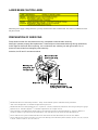
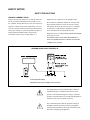
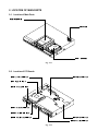
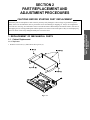
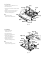
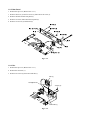
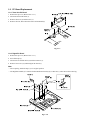
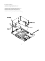
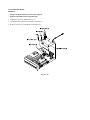
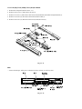
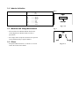
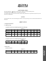
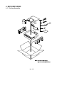
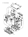
FILE NO. 810-200511
SERVICE MANUAL
DIGITAL VIDEO
HDD/DVD VIDEO RECORDER
RD-XS34SU
RD-XS34SC
S
Feb.,
2005
DOCUMENT CREATED IN JAPAN
Feb.,
2005
LASER BEAM CAUTION LABEL
When the power supply is being turned on, you may not remove this laser cautions label. If it removes, radiation of a laser
may be received.
PREPARATION OF SERVICING
Pickup Head consists of a laser diode that is very susceptible to external static electricity.
Although it operates properly after replacement, if it was subject to electrostatic discharge during replacement,
its life might be shortened. When replacing, use a conductive mat, soldering iron with ground wire, etc. to
protect the laser diode from damage by static electricity.
And also, the LSI and IC are same as above.
Ground conductive
wrist strap for body.
Soldering iron
with ground wire
or ceramic type
1M
W
Conductive mat
The ground resistance
between the ground line
and the ground is less than 10
·
·
·
·
·
·
W
.
Manufactured under license from Dolby Laboratories. “Dolby” and the double-D symbol are trademarks of Dolby Laboratories.
“DTS” and “DTS Digital Out” are trademarks of Digital Theater Systems, Inc.
Manufactured under license from QSound Labs, Inc. U.S. patent Nos. 5,105,462, 5,208,860 and 5,440,638 and various foreign counterpart. Copyright
QSound Labs, Inc. 1998-2002. QXpanderTM is a trademark of QSound Labs, Inc. All rights reserved.
In the United States, TV GUIDE and other related marks are registered marks of Gemstar-TV Guide International, Inc. and/or of its affiliates. In
Canada, TV GUIDE is a registered mark of Transcontinental Inc., and is used under license by Gemstar-TV Guide International, Inc.
The TV Guide On Screen system is manufactured under license from Gemstar-TV Guide International, Inc. and/or one of its affiliates.
The TV Guide On Screen system is protected by one or more of the following issued United States patents 6,498,895, 6,418,556, 6,331,877, 6,239,794;
6,154,203; 5,940,073; 4,908,713; 4,751,578; 4,706,121.
SAFETY NOTICE
SAFETY PRECAUTIONS
LEAKAGE CURRENT CHECK
Plug the AC line cord directly into a 120V AC outlet (do
not use an isolation transformer for this check). Use an
AC voltmeter, having 5000 W per volt or more sensitivity.
Connect a 1500 W 10 W resistor, paralleled by a 0.15 mF
150V AC capacitor between a known good earth ground
(water pipe, conduit, etc.) and all exposed metal parts of
cabinet (antennas, handle bracket, metal cabinet
screwheads, metal overlays, control shafts, etc.).
Measure the AC voltage across the 1500 W resistor.
The test must be conducted with the AC switch on and
then repeated with the AC switch off. The AC voltage
indicated by the meter may not exceed 0.3 V. A reading
exceeding 0.3 V indicates that a dangerous potential
exists, the fault must be located and corrected.
Repeat the above test with the DVD VIDEO RECORDER
power plug reversed.
NEVER RETURN A DVD VIDEO RECORDER TO
THE CUSTOMER WITHOUT TAKING NECESSARY
CORRECTIVE ACTION.
READING SHOULD NOT EXCEED 0.3V
AC VOLTMETER
DVD VIDEO RECORDER
(5000
W per volt
or more sensitivity)
Good earth ground
1500
W
such as a water pipe,
conduit, etc.
10 W
AC OUTLET
0.15
mF 150V AC
Test all exposed metal.
Voltmeter Hook-up for Leakage Current Check
The lightning flash with arrowhead symbol, within an
equilateral triangle, is intended to alert the user to the
presence of uninsulated “dangerous voltage” within the
product’s enclosure that may be of sufficient magnitude to
constitute a risk of electric shock to persons.
The exclamation point within an equilateral triangle is
intended to alert the user to the presence of important
operating and maintenance (servicing) instructions in the
literature accompanying the appliance.
CONTENTS
SECTION 1
GENERAL DESCRIPTIONS
2. LOCATION OF MAIN PARTS
2-1. Location of Main Parts
2-2. Location of PC Boards
1. OPERATING INSTRUCTIONS
SECTION 2
PART REPLACEMENT AND ADJUSTMENT PROCEDURES
1. Replacement of Mechanical Parts
1-1. Cabinet Replacement
1-1-1. Top Cover
1-1-2. HDD
1-1-3. Front Panel
1-1-4. RAM Diver
1-1-5. Rear Panel
1-1-6. Fan
1-2. PC Board Replacement
1-2-1. Tuner Unit PC Board
1-2-2. Digital PC Board
1-2-3. Mother PC Board
1-2-4. Power PC Board
1-2-5. Front (R), Front (L/SW), Front (Jack) PC Board
2. WIRING CONNECTION DIAGRAM
SECTION 3
SERVICING DIAGRAMS
1. CIRCUIT SYMBOLS AND
SUPPLEMENTARY EXPLANATION
1-1. Precautions for Part Replacement
1-2. Solid Resistor Indication
1-3. Capacitance Indication
1-4. Inductor Indication
1-5. Waveform and Voltage Measurement
1-6. Others
2. PRINTED WIRING BOARD AND
SCHEMATIC DIAGRAM
3. BLOCK DIAGRAMS
3-1. Overall Block Diagram
4. CIRCUIT DIAGRAMS
4-1. Power Supply Circuit Diagram
4-2. Front Circuit Diagram
4-2-1. Front Jack Circuit Diagram
4-2-2. Front Circuit Diagram (L/SW), (R)
4-3. Digital Circuit Diagram
4-3-1. Digital 1 Circuit Diagram
4-3-2. Digital 2 Circuit Diagram
4-4. Mother Circuit Diagram
4-4-1. Tuner Circuit Diagram
4-4-2. Timer Circuit Diagram
4-4-3. Audio Circuit Diagram
4-4-4. Video Circuit Diagram
4-4. Tuner Unit Circuit Diagram
5. PC BOARDS
5-1. Front Jack PC Board
5-2. Front Switch PC Board
5-3. Front (L) PC Board
5-4. Front (R) PC Board
5-5. Front Center PC Board
5-6. Digital PC Board
5-7. Mother PC Board
SECTION 4
PARTS LIST
SAFETY PRECAUTION
NOTICE
ABBREVIATIONS
1. Integrated Circuit (IC)
2. Capacitor (Cap)
3. Resistor (Res)
4. EXPLODED VIEWS
4-1. Packing Assembly
4-2. Chassis Assembly
5. PARTS LIST
1. OPERATING INSTRUCTIONS
Please refer to the owner's manual about the contents.
SECTION 1
GENERAL DESCRIPTIONS
SECTION 1
GENERAL DESCRIPTIONS
2. LOCATION OF MAIN PARTS
2-1. Location of Main Parts
RAM1 RAM DRIVE
ZG45 FAN
HDD1 HDD UNIT
Fig. 1-2-1
2-2. Location of PC Boards
EU05 Mother PC board
EU82 Tuner Unit PC Board
EU01 Digital PC Board
EU03B Front (L) PC Board
EU55 Front (Jack) PC Board
EU03D Front (SW) PC Board
EU03C Front (Center) PC Board
EU02 Power PC board
EU03A Front (R) PC Board
Fig. 1-2-2
SECTION 2
PART REPLACEMENT AND
ADJUSTMENT PROCEDURES
CAUTIONS BEFORE STARTING PART REPLACEMENT
Electronic parts are susceptible to static electricity and may easily damaged, so do not forget to ground as required.
Many screws are used inside the unit. To prevent the screws from missing or dropping, etc. always use a magnetized
screwdriver in servicing. Several kinds of screws are used and some of them need special cautions. That is, take care of
the tapping screws securing molded parts and fine pitch screws used to secure metal parts. If they are used improperly,
the screw holes will be easily damaged and the parts can not be fixed.
1-1. Cabinet Replacement
1-1-1. Top Cover
1. Remove seven screws (1), then remove the top cover (2).
Screws (1)
Screws (1)
Top cover (2)
Screws (1)
Fig. 2-1-1
SECTION 2
PART REPLACEMENT AND
ADJUSTMENT PROCEDURES
1. REPLACEMENT OF MECHANICAL PARTS
1-1-2. HDD
1. Remove the top cover. (Refer to item 1-1-1.)
2. Peel off three tapes (1).
3. Remove four screws (2).
4. Disconnect the flexible cable (3) and the connector (4).
5. Remove four screws (5), then remove the dampers (7) and HDD (8).
Note:
• After replacing, attach the tape (1) to its original position.
Tape (1)
Flexible
HDD (8)
cable (3)
Connector
Claw
Screw (5)
Flexible
cable (3)
Damper (7)
Screws (2)
Connector (4)
Screw (5)
HDD bracket (6)
Damper (7)
Damper (7)
Damper (7)
Screw (5)
Screws (2)
Damper (7)
Screw (5)
Damper (7)
Tapes (1)
Fig. 2-1-2
1-1-3. Front Panel
1. Remove the top cover. (Refer to item 1-1-1.)
Tape (1)
Flexible
2. Peel off three tapes (1).
Connector (2)
3. Disconnect two connectors (2) and two flexible
cables (3).
cable (3)
Tape (1)
4. Remove two screws (4) and two bases (5).
5. Remove two screws (6) and four claws,
then remove the front panel (7).
Note:
Flexible
Claw
cable (3)
• After replacing, attach
the tape (1) to its original position.
Connector (2)
Tape (1)
Bases (5)
Claws
Screws (6)
Claw
Screws (4)
Front panel (7)
Fig. 2-1-3
1-1-4. RAM Drive
1. Remove the front panel.
(Refer to item 1-1-3.)
Connector (5)
Tapes (1)
2. Peel off three tapes (1).
Flexible
cable (2)
3. Disconnect four flexible cable (2)
4. Remove three screws (3),
then remove the RAM drive (4).
5. Remove the connector (5).
6. Remove four screws (6),
then remove the fixing bracket (7).
Connector
RAM drive (4)
Screw (3)
cable (2)
Screws (6)
Screw (3)
Note:
• After replacing, attach
the tape (1) to its original position.
Flexible
Tape (1)
fixing bracket (7)
Screw (3)
Screws (6)
Fig. 2-1-4
1-1-5. Rear Panel
1. Remove the top cover. (Refer to item 1-1-1.)
1. Remove the screw (1) and five screws (2), then remove the screw (3).
2. Remove the bush from the rear panel (4).
3. Remove two claws, then remove the rear panel (4).
4. Remove two screws (5) and the fan (6).
Screw (1)
Screws (2)
Rear panel (4)
Claw
Screw (3)
Screws (5)
Bush
Fan (6)
Hexagonal nut
Fig. 2-1-5
1-1-6. Fan
1. Remove the top cover. (Refer to item 1-1-1.)
2. Remove the connector (1).
3. Remove two screws (2), then remove the fan (3).
Fan (3)
Hexagonal nuts
Screws (2)
Connector (1)
Fig. 2-1-6
Claw
1-2. PC Board Replacement
1-2-1. Tuner Unit PC Board
1. Remove the top cover. (Refer to item 1-1-1.)
Tuner Unit PC board (4)
Screw (3)
2. Disconnect the flexible cable (1).
3. Remove the screw (2) and the screw (3).
4. Remove the claw, then remove the Tuner Unit PC Board (4).
Screw (2)
Flexible
cable (1)
Claw
Fig. 2-1-7
1-2-2. Digital PC Board
1. Remove the top cover. (Refer to item 1-1-1.)
2. Peel off the tape (1).
3. Disconnect two flexible cables (2) and the connector (3).
4. Remove four screws (4), and the Digital PC board (5).
Note:
• After replacing, attach the tape (1) to its original position.
• The Digital PC Board (5) is connected to the Mother PC board (6) by a connector (7). Take notice when removing.
Tape(1)
Flexible
Flexible
cable (2)
cables (2)
Claws
Connector (3)
A
A
Screws (4)
Connector
Digital PC board (5)
Connector (7)
Connectors (7)
Mother PC board (6)
Fig. 2-1-8
1-2-3. Mother PC Board
1. Remove the front panel. (Refer to item 1-1-3.)
2. Remove the rear panel. (Refer to item 1-1-5.)
3. Remove the Tuner Unit PC board. (Refer to item 1-2-1.)
4. Remove the Digital PC board. (Refer to item 1-2-2.)
5. Disconnect two flexible cable (1) and the connector (2).
6. Remove six screws (3), then remove the Mother PC board (4).
Screws (3)
Mother PC board (4)
Connector (2)
Flexible
cables (1)
Fig. 2-1-9
1-2-4. Power PC Board
Cautions :
• Danger of explosion if battery is incorrectly replaced.
• Replace only with the same or equivalent type.
1. Remove the top cover. (Refer to item 1-1-1.)
2. Disconnect three connectors (1) and the connector (2).
3. Remove four screws (3) and the Power PC board (4).
Connectors (1)
Screws (3)
Connector (1)
Connector (2)
Power PC board (4)
Fig. 2-1-10
1-2-5. Front (R), Front (L/SW), Front (Jack) PC Board
1. Remove the front panel. (Refer to item 1-1-3.)
2. Remove four screws (1), then remove the stay (2).
3. Remove six screws (3), then remove the Front (Center) PC Board (4) and the Front (R) PC Board (5).
5. Remove two screws (6), then remove the Front (Jack) PC board (7).
4. Remove four screws (8), then remove the Front (L/SW) PC board (9).
Front (Jack)
PC board (7)
Screws (1)
Screws (8)
Front (L) PC board (9)
Screws (6)
Screw (3)
Stay (2)
Front (SW)
PC board
Front (Center)
PC board (4)
Front panel
Front (R) PC board (5)
Fig. 2-1-11
Note:
• Fasten with the tape, taking care so that the wire does not hang over the tray door.
Stay
Operation
panel door
Wire
Fasten with
the tape.
Fasten with
the tape.
Front (R) PC board
Front (Center)
PC board
Fig. 2-1-12
Front (Jack)
Front (L)
PC board
PC board
2. WIRING CONNECTION DIAGRAM
After the servicing is complete, return the wiring to its original state by using the below diagram as a reference.
Tuner Unit PC Board
Mother PC Board
FAN
Power PC Board
W202
W003
W201
W005
HDD
W006
W301
Front Panel
W001
Digital PC Board
RAM Drive
: Tape
: Flexible cable
Fig. 2-2-1
W202
SECTION 3
SERVICING DIAGRAMS
1. CIRCUIT SYMBOLS AND SUPPLEMENTARY EXPLANATION
1-1. Precautions for Part Replacement
• In the schematic diagram, parts marked
(ex.
F801) are critical part to meet the safety regulations,
so always use the parts bearing specified part codes
(SN) when replacing them.
• Using the parts other than those specified shall violate
the regulations, and may cause troubles such as
operation failures, fire etc.
1-2. Solid Resistor Indication
Unit
Tolerance
Rated Wattage
Type
Eg. 1
100k
Rated Wattage
Type
Tolerance
Fig. 3-1-1
1-3. Capacitance Indication
Symbol
+
........... Electrolytic, Special electrolytic
........... Non polarity electrolytic
........... Ceramic, plastic
M
........... Film
........... Trimmer
None ........... F
m
........... mF
p
........... pF
None ........... 50V
For other than 50V and electrolytic capacitors,
described in the Circuit Diagram.
(1) Ceramic, plastic, and film capacitors of which
capacitance are more than 10 pF.
None ........... ±5% or more
B
........... ±0.1%
C
........... ±0.25%
D
........... ±0.5%
F
........... ±1%
G
........... ±2%
(2) Ceramic, plastic, and film capacitors of which
capacitance are 10 pF or less.
None ........... more than ±5 pF
B
........... ±0.1 pF
C
........... ±0.25 pF
(3) Electrolytic, Trimmer
Tolerance is not described.
None ........... SL
For others, temperature characteristics are
described. (For capacitors of 0.01 mF and
no indications are described as F.)
Sometimes described with abbreviated letters as
shown in Eg. 3.
NP
Unit
Rated voltage
Tolerance
Temperature characteristic
(Ceramic capacitor)
Static electricity capacity
(Ceramic capacitor)
Eg. 2
100m
Temperature Rated
response
voltage
Tolerance
Fig. 3-1-2
Eg. 3
104
4
m
10x10 pF (0.1 F)
Temperature characteristic
(or Temperature characteristic+
Static electricity capacity tolerance)
Fig. 3-1-3
SECTION 3
SERVICING DIAGRAMS
None ........... W
K
........... kW
M
........... MW
None ........... ±5%
B
........... ±0.1%
C
........... ±0.25%
D
........... ±0.5%
F
........... ±1%
G
........... ±2%
K
........... ±10%
M
........... ±20%
(1) Chip Parts
None ......... 1/16W
(2) Other Parts
None ......... 1/6W
Other than above, described in the Circuit Diagram.
None ........... Carbon film
S
........... Solid
R
........... Oxide metal film
M
........... Metal film
W
........... Cement
FR
........... Fusible
1-4. Inductor Indication
Unit
Tolerance
None
m
m
None
B
C
D
F
G
K
M
........... H
........... mH
........... mH
........... ±5%
........... ±0.1%
........... ±0.25%
........... ±0.5%
........... ±1%
........... ±2%
........... ±10%
........... ±20%
Eg. 4
Type name
Fig. 3-1-4
1-5. Waveform and Voltage Measurement
Eg. 5
• The waveforms for CD/DVD and RF shown in the
circuit diagrams are obtained when a test disc is
played back.
• All voltage values except the waveforms are expressed
in DC and measured by a digital voltmeter.
10m
Type
Tolerance
1-6. Others
• The parts indicated with "NC" or "KETU" etc. are not
used in the circuits of this model.
Fig. 3-1-5
SECTION 4
PARTS LIST
SAFETY PRECAUTION
The parts identified by ! ( ) mark are critical for safety. Replace only with part number specified.
The mounting position of replacement is to be identical with originals.
The substitute replacement parts which do not have the same safety characteristics as specified in the parts list may create
shock, fire or other hazards.
NOTICE
The part number must be used when ordering parts in order to assist in processing, be sure to include the model number and
description.
ABBREVIATIONS
1. Integrated Circuit (IC)
2. Capacitor (Cap)
• Capacitance Tolerance (for Nominal Capacitance more than 10pF)
Table 4-2-1
Symbol
B
C
D
F
G
J
K
M
N
Tolerance %
± 0.1
± 0.25
± 0.5
±1
±2
±5
± 10
± 20
± 30
Symbol
P
Q
T
U
V
W
X
Y
Z
Tolerance %
+ 100
0
+ 30
– 10
+ 50
– 10
+ 75
– 10
+ 20
– 10
+ 100
– 10
+ 40
– 20
+ 150
– 10
+ 80
– 20
Ex. 10µF J = 10µF ± 5%
• Capacitance Tolerance (for Nominal Capacitance 10pF or less)
Table 4-2-2
Symbol
B
C
D
F
G
Tolerance pF
± 0.1
± 0.25
± 0.5
±1
±2
Ex. 10pF G = 10pF ± 2pF
3. Resistor (Res)
• Resistance tolerance
Table 4-3-1
B
C
D
F
G
J
K
M
Tolerance %
± 0.1
± 0.25
± 0.5
±1
±2
±5
± 10
± 20
Ex. 470WJ = 470W± 5%
SECTION 4
PARTS LIST
Symbol
4. EXPLODED VIEWS
4-1. Packing Assembly
ZF10
ZF11
ZF12
ZF13
ZF01
ZF35
DVD
-RO
M
Note: The shape of the packing
material is sometimes different.
Fig. 4-4-1
4-2. Chassis Assembly
ZG20
EU82
W003
RAM1
W005
EU01
W501
ZG45
W002
W001
EU05
W006
EU02
HDD1
W502
ZG50
EU03B
EU55
ZG01
EU03C
EU03D
W008
W004
EU03A
Fig. 4-4-2
P801
5. PARTS LIST
Location
No.
Part No.
Description
- MECHANICAL PARTS -
!
!
!
!
!
!
!
!
HDD1
P801
RAM1
W001
W002
W003
W004
W005
W006
W008
W501
W502
ZF01
ZF10
ZF11
ZF10
ZF11
ZF12
ZF13
ZF35
ZG01
ZG20
ZG45
ZG50
P000428190
P000416780
P000432490
P000433830
P000433810
P000433800
P000433840
P000433820
P000387340
P000433850
P000401270
P000401270
P000432480
P000416460
P000416470
P000417050
P000417060
P000416480
P000416490
P000416800
P000432580
P000432500
P000432510
P000416790
HDD,ST3160022ACECS 160GB
Cord,Power
UL
DVD-RAM
SW-9573-ETS
Cable,Flexible
FFC,10P,L400
Cable,Flexible
FFC,11P,L120
Cable,Flexible
FFC,11P,L60
Cable,Flexible
FFC,9P,L430
Cable,Flexible
FFC,40P,L280
Cable,Flexible
FFC,40P,L360
Cable,Flexible
FFC,11P,L430
Conv Unit,ATAPI-FFC
Conv Unit,ATAPI-FFC
Remote Control Unit,SE-R0144
Owners Manual,ST
English,RD-XS34SU
Owners Manual,OP
English,RD-XS34SU
Owners Manual,ST
French,RD-XS34SC
Owners Manual,OP
French,RD-XS34SC
Owners Manual,Quick,English
Owners Manual,Quick,Spanish,RD-XS34SU
IR Blaster
RWS1000-0062E
Front Panel
Cover,Top
Fan,DC
AFB0512LDP48Z
Damper
Location
No.
Part No.
Description
- ELECTRICAL PARTS -
!
EU01
EU01
P000432530
P000432470
IC303
IC304
IC305
IC307
IC309
IC310
IC311
IC312
IC314
IC315
IC317
IC603
P000416750
P000391280
P000391240
P000391230
P000378040
79040306
P000391210
P000391210
P000391210
P000391210
P000377920
79040074
Q301
Q302
Q303
Q304
Q305
Q306
Q307
Q308
Q309
79050018
79050018
79050018
79050018
79050018
79050016
79050016
79050018
79050018
X301
X302
X303
79089168
79089168
P000377990
PC Board Assy
Digital,RD-XS34SU
PC Board Assy
Digital,RD-XS34SC
- INTEGRATED CIRCUITS IC
BA25BC0FP
IC
PQ070XZ01ZPH
IC
NJM2125F
IC
UPD72852AGB-8EU
IC
SN74AHC1G08HDCKR
IC
PST594JMT
IC
K4H560838D-TCB000
IC
K4H560838D-TCB000
IC
K4H560838D-TCB000
IC
K4H560838D-TCB000
IC
SN74LV244APWR
IC
TC74HCU04AF
- TRANSISTORS Transistor,Chip
2SA1162
Transistor,Chip
2SA1162
Transistor,Chip
2SA1162
Transistor,Chip
2SA1162
Transistor,Chip
2SA1162
Transistor,Chip
2SC2712
Transistor,Chip
2SC2712
Transistor,Chip
2SA1162
Transistor,Chip
2SA1162
- MISCELLANEOUS Oscillator,Crystal
Oscillator,Crystal
Crystal
27.0M
EU02
P000432520
PC Board Assy
EU03A
P000432560
IC101
IC102
IC103
P000416700
P000402790
79050015
D110
D111
D112
D113
D114
D115
D116
D119
79060028
79060028
79060028
79060028
79060028
79060028
79060028
79060028
A100
P000416630
PC Board Assy
Front(R)
- INTEGRATED CIRCUITS IC
PT6315
IR Module
GP1UM261RKOF
Transistor,Chip
HN1B01F
- DIODES Diode,Chip
1SS226
Diode,Chip
1SS226
Diode,Chip
1SS226
Diode,Chip
1SS226
Diode,Chip
1SS226
Diode,Chip
1SS226
Diode,Chip
1SS226
Diode,Chip
1SS226
- MISCELLANEOUS Display,FL
HNV-10SM38T
EU03B
P000432550
Q100
Q101
Q102
Q103
Q108
Q109
Q110
79050009
79050009
79050009
79050009
79050089
79050089
79050009
PC Board Assy
- TRANSISTORS Transistor,Chip
Transistor,Chip
Transistor,Chip
Transistor,Chip
Transistor
Transistor
Transistor,Chip
Power
Front(L)
RN1401
RN1401
RN1401
RN1401
RN2401
RN2401
RN1401
Location
No.
Part No.
Description
D103
D104
D105
D121
D128
79060077
P000416660
79060091
79060033
P000416670
S100
S101
S102
S103
S104
S105
S106
S107
S108
S109
S110
P000391050
P000391050
P000391050
P000391050
P000391050
P000391050
P000391050
P000391050
P000391050
P000391050
P000391050
- DIODES Diode,LED
Diode,LED
Diode,LED
Diode,LED
Diode,LED
- MISCELLANEOUS Switch,Tact
Switch,Tact
Switch,Tact
Switch,Tact
Switch,Tact
Switch,Tact
Switch,Tact
Switch,Tact
Switch,Tact
Switch,Tact
Switch,Tact
EU03C
D106
D107
P000437410
79060091
79060091
PC Board Assy
Diode,LED
Diode,LED
Front Center(LED)
LED, MVL-354B-T
LED, MVL-354B-T
EU03D
P000437400
PC Board Assy
Front Switch(Jog)
EU05
P000432540
IC701
IC702
IC902
IC903
ICA01
ICA03
ICB10
ICW01
ICX01
ICX31
ICX32
P000391180
P000391150
P000416730
P000416650
P000416760
79040397
P000395150
P000391260
P000401210
79040371
P000363370
Q700
Q701
Q904
Q905
Q906
Q908
QB08
QW02
QW03
QW04
QX06
QX09
QX31
QX32
79050016
79050018
79050001
79050100
79050001
79050014
79050016
79050100
79050018
79050018
79050018
79050018
79050016
79050100
D701
D702
D703
D704
D901
D902
DB06
79060019
79060028
79060028
79060028
79060019
79060019
79060096
PC Board Assy
Mother
- INTEGRATED CIRCUITS IC
PST3222NR
IC
DC74HCT125M
IC
NJM2115M
IC,Terminal,OPT
LAF1001-0301F
IC
PCM1851PJT
IC
MM1575ANRE
IC
MM1565AFBE
IC
MM1568DJBEG
IC
MM1656XJBE
IC
BA7046F
IC
NJM2330MV
- TRANSISTORS Transistor,Chip
2SC2712
Transistor,Chip
2SA1162
Transistor,Chip
RN2402
Transistor,Chip
RN1402
Transistor,Chip
RN2402
Transistor,Chip
HN1C03F
Transistor,Chip
2SC2712
Transistor,Chip
RN1402
Transistor,Chip
2SA1162
Transistor,Chip
2SA1162
Transistor,Chip
2SA1162
Transistor,Chip
2SA1162
Transistor,Chip
2SC2712
Transistor,Chip
RN1402
- DIODES Diode,Chip
1SS355
Diode,Chip
1SS226
Diode,Chip
1SS226
Diode,Chip
1SS226
Diode,Chip
1SS355
Diode,Chip
1SS355
Diode,Zener
MTZJT-7733D
- MISCELLANEOUS -
SLA-360MT
EL-3105-1UYOC/S530
LED, MVL-354B-T
EL-3105-1VRT
Location
No.
!
Part No.
Description
B701
J702
JW01
JX01
X700
X701
P000377950
P000432600
P000402770
P000401100
P000391040
P000363400
Buzzer
PS1240P02AT
Jack
3.5 Small
Jack,6P+2Y/C
Jack Board,6P+2P Y/C
Crystal
Oscillator,Crystal
EU82
P000432570
Tuner
MB01
P000416770
PC Board Assy
- MISCELLANEOUS Tuner
EU55
P000432590
Front(Jack)
J170
J171
P000387300
P000402780
PC Board Assy
- MISCELLANEOUS Jack,DV
Jack,3P+1Y/C
ENGF6501G
SPECIFICATIONS
Power requirement during operation
34W
Power requirement at standby
17W or below (Front panel display: on)
16W or below (Front panel display: off)
Power supply
120V AC, 60 Hz
Mass
5.4kg
External dimension
Width 430 x Height 62 x Depth 334mm
Incoming channels
TV : 2-69CH, Cable : 1-125CH
Antenna input/output terminal
VHF/UHF : 75W, F Connector
Signal system
Standard NTSC Color TV system
Laser
Semiconductor laser, Wavelength : 650nm/780nm
Format
DVD-Video format
Image recording system
MPEG2
Sound recording system
Dolby Digital M1, M2, Linear PCM
Internal hard disk
160 GB
VIDEO input
1.0Vp-p (75W), Sync signal negative, Pin jack x 3 systems, 2 at rear, 1 in front
VIDEO output
1.0Vp-p (75W), Sync signal negative, Pin jack x 2 systems, 1 at rear
S-VIDEO input
(Y) 1.0Vp-p (75W), Sync signal negative, Mini DIN4 Pin x 3 systems
(C) 0.286Vp-p (75W), 2 at rear, 1 in front
S-VIDEO output
(Y) 1.0Vp-p (75W), Sync signal negative, Mini DIN4 Pin x 2 systems
(C) 0.286Vp-p (75W), 1 at rear
COMPONENT output(Y, PB, PR)
Y output (green), 1.0Vp-p (75W), Sync signal negative, Pin jack x 1 system
PB, PR output (blue, red), 0.7Vp-p (75W), Pin jack x 1 systems each
AUDIO input
2.0V (rms), 22kW or above, pin jack (L, R) x 3 systems
2 at rear, 1 in front
AUDIO output
2.0V (rms), 2.2kW or below, pin jack (L, R) x 1 systems
1 at rear
DIGITAL AUDIO OUTPUT BITSTREAM/PCM
(OPTICAL terminal)
Optical connector x 1 system
G-LINK jack
This is for connection of the supplied IR control cable only.
DV input
4-Pin x 1 in front
Remote control
Wireless remote control (SE-R0144)
Operating conditions
Temperature: 41°F~95°F (5°C~35°C),
Position: Horizontal
Clock display
12 hour digital display
Clock accuracy
Quartz (monthly deviation: approximately ±30 seconds)
• The design and specifications may change without prior notice.
• The Illustrations and screens described in this manual may be exaggerated or simplified for easy recognition and may be slightly different from the actual unit.
1 1, SHIBAURA 1 CHOME, MINATO KU, TOKYO 105 8001, JAPAN


![Shigella Polyvalent Agglutinating Sera [FR]](http://vs1.manualzilla.com/store/data/006511038_1-3032f95bd4b5f04e9e2fa304420d118e-150x150.png)