1
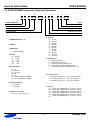
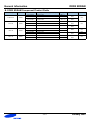
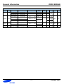
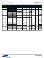
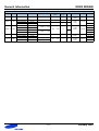
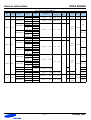
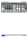
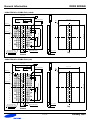
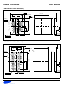
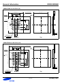
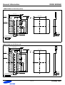
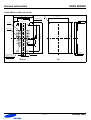
General Information
DDR2 SDRAM
DDR2 SDRAM Product Guide
January 2009
Memory Division
1 of 17
January 2009
General Information
DDR2 SDRAM
A. DDR2 SDRAM Component Ordering Information
1
2
3
4
5
6
7
8
9
10
11
K 4 T X X X X X X X - X X X X
SAMSUNG Memory
Speed
DRAM
Temp & Power
DRAM Type
Package Type
Revision
Density
Bit Organization
Interface (VDD, VDDQ)
# of Internal Banks
8. Revision
1. SAMSUNG Memory : K
M
A
B
C
D
E
F
G
H
Q
R
2. DRAM : 4
3. DRAM Type
T : DDR2 SDRAM
4. Density
56 : 256Mb
51 : 512Mb
1G :
1Gb
2G :
2Gb
4G :
4Gb
9. Package Type
Z
J
H
M
T
5. Bit Organization
04
06
07
08
16
26
27
:x4
: x 4 Stack
: x 8 Stack
:x8
: x16
: x 4 Stack (JEDEC Standard)
: x 8 Stack (JEDEC Standard)
: 1st Gen.
: 2nd Gen.
: 3rd Gen.
: 4th Gen.
: 5th Gen.
: 6th Gen.
: 7th Gen.
: 8th Gen.
: 9th Gen.
: 17th Gen.
: 18th Gen.
:
:
:
:
:
FBGA (Lead-free)
FBGA DDP (Lead-free)
FBGA (Lead-free & Halogen-free)
FBGA DDP (Lead-free & Halogen-free)
FBGA DSP (Lead-free & Halogen-free, Thin)
10. Temp & Power
C : Commercial Temp.( 0°C ~ 95°C) & Normal Power
L : Commercial Temp.( 0°C ~ 95°C) & Low Power
Y : Commercial Temp.( 0°C ~ 95°C) & Low Voltage
6. # of Internal Banks
3 : 4 Banks
4 : 8 Banks
7. Interface ( VDD, VDDQ)
Q : SSTL-1.8V (1.8V, 1.8V)
11. Speed
CC : DDR2-400 (200MHz @ CL=3, tRCD=3, tRP=3)
D5 : DDR2-533 (266MHz @ CL=4, tRCD=4, tRP=4)
E6 : DDR2-667 (333MHz @ CL=5, tRCD=5, tRP=5)
F7 : DDR2-800 (400MHz @ CL=6, tRCD=6, tRP=6)
E7 : DDR2-800 (400MHz @ CL=5, tRCD=5, tRP=5)
F8 : DDR2-1066(533MHz @ CL=7, tRCD=7, tRP=7)
2 of 17
January 2009
General Information
DDR2 SDRAM
B. DDR2 SDRAM Component Product Guide
Density
512Mb G-die
1Gb Q-die
1Gb E-die
2Gb A-die
Banks
4Banks
8Banks
8Banks
8Banks
Part Number
Package & Power, Temp. (-C/-L) & Speed
Org.
K4T51043QG
HC(L)E7/F7/E6
128M x 4
K4T51083QG
HC(L)E7/F7/E6
64M x 8
K4T51163QG
HC(L)E7/F7/E6
32M x 16
K4T1G044QQ
HC(L)E7/F7/E6
256M x 4
K4T1G084QQ
HC(L)E7/F7/E6
128M x 8
K4T1G164QQ
HC(L)E7/F7/E6
K4T1G044QE
HC(L)E7/F7/E6
256M x 4
K4T1G084QE
HC(L)E7/F7/E6
128M x 8
64M x 16
K4T1G164QE
HC(L)E7/F7/E6
K4T1G164QE
HC(L)F8
K4T2G044QA
HC(L)F7/E6
512M x 4
K4T2G084QA
HC(L)F7/E6
256M x 8
3 of 17
64M x 16
PKG
60 ball
FBGA
Avail.
Now
84 ball
FBGA
60 ball
FBGA
Now
84 ball
FBGA
60 ball
FBGA
84 ball
FBGA
68 ball
FBGA
Now
Now
Feb.’09
Now
January 2009
General Information
DDR2 SDRAM
C. DDR2 SDRAM Module Ordering Information
1
2
3
4
5
6
7
8
9
10
11
12
13
M X X X T X X X X X X X - X X X X
Memory Module
AMB Vendor
DIMM Type
Data bits
DRAM Component Type
Speed
Temp & Power
PCB Revision
Depth
# of Banks in Comp. & Interface
Package
Bit Organization
Component Revision
1. Memory Module : M
8. Component Revision
M : 1st Gen.
B : 3rd Gen.
D : 5th Gen.
F : 7th Gen.
Q : 17th Gen.
2. DIMM Type
3 : DIMM
4 : SODIMM
3. Data Bits
78 :
91 :
92 :
93 :
95 :
70 :
x64
x72
x72
x72
x72
x64
T : DDR2 SDRAM (1.8V VDD)
Z
J
Q
H
M
E
32 : 32M
64 : 64M
28 : 128M
56 : 256M
51 : 512M
1G : 1G
33
65
29
57
52
1K
: 32M (for 128Mb/512Mb)
: 64M (for 128Mb/512Mb)
: 128M (for 128Mb/512Mb)
: 256M (for 512Mb/2Gb)
: 512M (for 512Mb/2Gb)
: 1G (for 2Gb)
6. # of Banks in comp. & Interface
4Banks & SSTL-1.8V
8Banks & SSTL-1.8V
7. Bit Organization
:
:
:
:
:
:
:
x4
x8
x16
x 4 Stack (JEDEC Standard)
x 8 Stack (JEDEC Standard)
x 4 Stack
x 8 Stack
:
:
:
:
:
:
FBGA(Lead-free)
FBGA DDP (Lead-free)
FBGA QDP (Lead-free)
FBGA (Lead-free & Halogen-free)
FBGA DDP (Lead-free & Halogen-free)
FBGA QDP (Lead-free & Halogen-free)
10. PCB Revision
0 : Mother PCB
2 : 2nd Rev.
4 : 4th Rev.
5. Depth
0
3
4
6
7
8
9
: 2nd Gen.
: 4th Gen.
: 6th Gen.
: 8th Gen.
: 18th Gen.
9. Package
240pin Unbuffered DIMM
240pin ECC unbuffered DIMM
240pin VLP Registered DIMM
240pin Registered DIMM
240pin Fully Buffered DIMM
200pin Unbuffered SODIMM
4. DRAM Component Type
5 :
6 :
A
C
E
G
R
1
3
A
S
:
:
:
:
1st Rev.
3rd Rev.
Parity DIMM
Reduced PCB
11. Temp & Power
C : Commercial Temp.( 0°C ~ 95°C) & Normal Power
L : Commercial Temp.( 0°C ~ 95°C) & Low Power
Y : Commercial Temp.( 0°C ~ 95°C) & Low Voltage
12. Speed
CC : DDR2-400 (200MHz @ CL=3, tRCD=3, tRP=3)
D5 : DDR2-533 (266MHz @ CL=4, tRCD=4, tRP=4)
E6 : DDR2-667 (333MHz @ CL=5, tRCD=5, tRP=5)
F7 : DDR2-800 (400MHz @ CL=6, tRCD=6, tRP=6)
E7 : DDR2-800 (400MHz @ CL=5, tRCD=5, tRP=5)
F8 : DDR2-1066(533MHz @ CL=7, tRCD=7, tRP=7)
13. AMB Vendor For FBDIMM
: Intel
5
: IDT
6, 8
3, 4, 9 : Montage
Note : PC2-8500(DDR2-1066). PC2-6400(DDR2-800), PC2-5300(DDR2-667)
PC2-4200(DDR2-533), PC2-3200(DDR2-400)
4 of 17
January 2009
General Information
DDR2 SDRAM
D. DDR2 SDRAM Module Product Guide
240Pin DDR2 Unbuffered DIMM
Org.
Density
64Mx 64
512MB
64Mx 72
128Mx 64
1GB
128Mx 72
256Mx 64
2GB
256Mx 72
512Mx 64
512Mx 72
4GB
Internal
Banks
Rank
PKG
4
1
60 ball
FBGA
Speed
M378T6553GZS
CE7/F7/E6
64M x 8 *
8pcs
512Mb
G-die
M378T6464QZ(H)3
CE7/F7/E6
64M x 16 *
4pcs
1Gb
Q-die
M378T6464EHS
CE7/F7/E6
64M x 16 *
4pcs
1Gb
E-die
M391T6553GZ3
CE7/F7/E6
64M x 8 *
9pcs
512Mb
G-die
4
1
64M x 8 * 16pcs 512Mb
G-die
4
2
8
1
M378T2953GZ3
CE7/F7/E6
M378T2863QZ(H)S
CE7/F7/E6
M378T2863EHS
CE7/F7/E6
M378T2863EHS
CF8
M391T2953GZ3
CE7/F7/E6
M391T2863QZ(H)3
CE7/F7/E6
M391T2863EH3
CE7/F7/E6
M378T5663QZ(H)3
CE7/F7/E6
M378T5663EH3
CE7/F7/E6
M378T5663EH3
CF8
M391T5663QZ(H)3
CE7/F7/E6
M391T5663EH3
CE7/F7/E6
Composition
Comp.
Version
Part Number
1Gb
128M x 8 *
8pcs
1Gb
64M x 8 * 18pcs 512Mb
128M x 8 * 18pcs
128M x 8 * 16pcs
128M x 8 * 18pcs
1
1
84 ball
FBGA
Avail.
30mm
Now
60 ball
FBGA
Q-die
E-die
G-die
1Gb
Q-die
1Gb
E-die
1Gb
Q-die
1Gb
E-die
1Gb
Q-die
1Gb
E-die
M378T5263AZ(H)3
CF7/E6
256M x 8 * 16pcs
2Gb
A-die
M391T5263AZ(H)3
CF7/E6
256M x 8 * 18pcs
2Gb
A-die
5 of 17
8
Height
Now
60 ball
FBGA
4
2
8
1
30mm
Feb. ’09
Now
Now
8
2
60 ball
FBGA
30mm
Feb. ’09
Now
8
2
68 ball
FBGA
30mm
Now
January 2009
General Information
DDR2 SDRAM
200Pin DDR2 SODIMM
Org.
64Mx 64
128Mx 64
Density
Part Number
Speed
M470T6554GZ3
C(L)E7/F7/E6
512MB M470T6464QZ(H)3
1GB
256Mx 64
2GB
512Mx 64
4GB
C(L)E7/F7/E6
M470T6464EHS
C(L)E7/F7/E6
M470T2953GZ3
C(L)E7/F7/E6
M470T2864QZ(H)3
C(L)E7/F7/E6
M470T2864EH3
C(L)E7/F7/E6
M470T2863EH3
C(L)E7/F7/E6
M470T5663QZ(H)3
C(L)E7/F7/E6
M470T5663EH3
C(L)E7/F7/E6
M470T5267AZ(H)3
C(L)F7/E6
Composition
32M x 16 *
64M x 16 *
64M x 8
8pcs
4pcs
* 16pcs
64M x 16 *
8pcs
128M x 8
*
128M x 8
* 16pcs
st.512M x 8
*
6 of 17
8pcs
8pcs
Comp.
Version
512Mb
G-die
1Gb
Q-die
1Gb
E-die
512Mb
G-die
1Gb
Q-die
1Gb
E-die
1Gb
Q-die
1Gb
E-die
2Gb
A-die
Internal
Banks
Rank
4
2
8
1
4
2
60 ball
FBGA
2
84 ball
FBGA
1
60 ball
FBGA
8
8
2
8
2
PKG
Height
Avail.
84 ball
FBGA
30mm
Now
30mm
Now
30mm
Now
30mm
Now
60 ball
FBGA
83 ball
FBGA
January 2009
General Information
DDR2 SDRAM
240Pin DDR2 Registered DIMM
Org.
Density
64Mx 72
512MB
128Mx 72
256Mx 72
512Mx 72
1Gx 72
1GB
2GB
4GB
8GB
Part Number
Speed
M393T6553GZ3
CD5/CC
M393T6553GZA
CF7/E6
M393T2953GZ3
CD5/CC
M393T2953GZA
CF7/E6
M393T2950GZ3
CD5/CC
M393T2950GZA
CF7/E6
M393T2863QZ3
CD5/CC
M393T2863QZA
CE7/F7/E6
M393T2863QHA
CE6/F7/E7
M393T5750GZ3
CD5/CC
M393T5750GZA
CF7/E6
M393T5663QZ3
CD5/CC
M393T5663QZA
CF7/E6
M393T5663QHA
CE6/F7/E7
M393T5660QZ3
CD5/CC
M393T5660QZA
CE7/F7/E6
M393T5660QHA
CE6/F7/E7
M393T5160QZ3
CD5/CC
M393T5160QZA
CE7/F7/E6
M393T5160QHA
CE6/F7/E7
M393T5260AZA
CF7/E6
M393T1G60QJA
CE6/D5
M393T1G60QMA
CE6/D5
M393T1K66AZA
CF7/E6
Composition
64M x 8 * 9pcs
Comp.
Version
Internal
Banks
Rank
PKG
Height
Avail.
1
60 ball
FBGA
30mm
Now
60 ball
FBGA
30mm
512Mb
G-die
4
512Mb
G-die
4
64M x 8 * 18pcs
2
128M x 4 * 18pcs
128M x 8 * 9pcs
1
1Gb
Q-die
8
Now
1
2Q. ’09
128M x 4 * 36pcs
512Mb
G-die
4
2
Now
128M x 8 * 18pcs
2
1Gb
Q-die
60 ball
FBGA
30mm
8
256M x 4 * 18pcs
2Q. ’09
Now
1
2Q. ’09
256M x 4 * 36pcs
1Gb
Q-die
2
60 ball
FBGA
8
512M x 4 * 18pcs
2Gb
A-die
1
68 ball
FBGA
DDP 512M x 4 * 36pcs
1Gb
Q-die
4
63 ball
FBGA
st.1G x 4 * 18pcs
2Gb
A-die
2
83 ball
FBGA
8
7 of 17
Now
30mm
2Q. ’09
Now
Now
30mm
2Q. ’09
Now
January 2009
General Information
DDR2 SDRAM
240Pin DDR2 VLP Registered DIMM
Internal
Banks
Rank
PKG
Height
Avail.
G-die
4
1
60 ball
FBGA
18.3mm
Now
512Mb
G-die
4
1
1Gb
Q-die
8
1
60 ball
FBGA
18.3mm
Density
Part Number
Speed
64Mx 72
512MB
M392T6553GZA
CF7/E6
64M x 8 * 9pcs
512Mb
M392T2950GZA
CF7/E6
128M x 4 * 18pcs
128Mx 72
1GB
M392T2863QZA
CF7/E6
M392T2863QHA
CF7/E6
128M x 8 * 9pcs
256Mx 72
2GB
512Mx 72
4GB
1Gx 72
8GB
M392T5660QZA
CF7/E6
M392T5660QHA
CF7/E6
M392T5663QZA
CF7/E6
M392T5663QHA
CF7/E6
Composition
Comp.
Version
Org.
256M x 4 * 18pcs
Q-die
M392T5160QJA
CF7/E6
CF7/E6
M392T1G60QQA
CE6/D5
QDP 1G x 4 * 18pcs
M392T1G60QEA
CE6/D5
QDP 1G x 4 * 18pcs
DDP 512M x 4 * 18pcs
8 of 17
Now
60 ball
FBGA
8
128M x 8 * 18pcs
M392T5160QMA
2Q. ’09
1
1Gb
Now
18.3mm
2
2Q. ’09
Now
2Q. ’09
1Gb
Q-die
8
2
63 ball
FBGA
18.3mm
1Gb
Q-die
8
4
65 ball
FBGA
18.3mm
Now
2Q. ’09
Now
2Q. ’09
January 2009
General Information
DDR2 SDRAM
240Pin DDR2 Fully Buffered DIMM(1.8V)
Org.
Density
Part Number
64Mx 72
512MB
M395T6553GZ4
M395T2953GZ4
M395T2863QZ4
128Mx 72
Speed
AMB
CE7/F7/E6
6 : IDT C1
CE6
5 : Intel D1
CE7/F7/E6
6 : IDT C1
CE6
5 : Intel D1
CE7/F7/E6
6 : IDT C1
CE7/F7/E6
8: IDT L4
CE6
1GB
CE7/F7/E6
M395T2863QH4
CE7/F7/E6
CE6
M395T5750GZ4
M395T5663QZ4
256Mx 72
M395T5663QH4
6 : IDT C1
CE7/F7/E6
8: IDT L4
CE6
CE6
512Mx 72
4GB
M395T5160QH4
CE7/F7/E6
M395T1G60QJ4
1Gx 72
8GB
M395T1G60QM4
M395T1K66AZ4
G-die
4
1
64M x 8 * 18pcs
512Mb
G-die
4
2
60 ball
FBGA
Height
Avail.
30.35mm
Now
Now
60 ball
128M x 8 *
9pcs
1Gb
Q-die
8
1
FBGA
30.35mm
2Q. ’09
128M x 4 * 36pcs
512Mb
G-die
4
2
Now
60 ball
128M x 8 * 18pcs
1Gb
Q-die
8
2
FBGA
30.35mm
8: IDT L4
2Q. ’09
9: Montage D1
6 : IDT C1
8: IDT L4
Now
5 : Intel D1
9: Montage D1
8: IDT L4
M395T5163QH4
512Mb
PKG
5 : Intel D1
CE6
CE7/F7/E6
M395T5263AZ4
6 : IDT C1
6 : IDT C1
M395T5163QZ4
9pcs
5 : Intel D1
9: Montage D1
CE7/F7/E6
CE6
Rank
9: Montage D1
CE7/F7/E6
CE7/F7/E6
Banks
8: IDT L4
6 : IDT C1
CE7/F7/E6
Internal
5 : Intel D1
5 : Intel D1
CE6
M395T5160QZ4
6 : IDT C1
CE6
CE7/F7/E6
64M x 8 *
Comp.
Version
5 : Intel D1
9: Montage D1
CE7/F7/E6
CE6
2GB
Composition
256M x 4 * 36pcs
2
1Gb
Q-die
FBGA
8
5 : Intel D1
60 ball
30.35mm
2Q. ’09
9: Montage D1
8: IDT L4
CF7/E6
6 : IDT C1
CF7/E6
8: IDT L4
CE6/F7
8: IDT L4
CF7/E6
8: IDT L4
CF7/E6/D5
6 : IDT C1
CF7/E6
8: IDT L4
128M x 8 * 36pcs
256M x 8 * 18pcs
2Gb
A-die
2
DDP 512M x 4 * 36pcs
1Gb
Q-die
4
8
st.1G x 4 * 18pcs
9 of 17
Now
4
2Gb
A-die
2
2Q. ’09
68 ball
Now
FBGA
63 ball
FBGA
83 ball
FBGA
Now
30.35mm
2Q. ’09
Now
January 2009
General Information
DDR2 SDRAM
240Pin DDR2 Fully Buffered DIMM(1.55V)
Org.
Density
128Mx 72
1GB
256Mx 72
2GB
512Mx 72
1Gx 72
4GB
8GB
Part Number
Speed
AMB
M395T2863QZ4
YE6
8: IDT L4
M395T2863QH4
YE6
8: IDT L4
M395T5663QZ4
YE6
8: IDT L4
M395T5663QH4
YE6
8: IDT L4
M395T5160QZ4
YE6
8: IDT L4
Composition
Comp.
Internal
Version
Banks
Rank
64M x 8 * 18pcs
1Gb
Q-die
8
1
128M x 8 * 18pcs
1Gb
Q-die
8
2
256M x 4 * 36pcs
2
M395T5160QH4
YE6
8: IDT L4
M395T5163QZ4
YE6
8: IDT L4
M395T5163QH4
YE6
8: IDT L4
M395T5263AZ4
YE6
8: IDT L4
256M x 8 * 18pcs
2Gb
A-die
M395T1K66AZ4
YE6
8: IDT L4
st.1G x 4 * 18pcs
2Gb
A-die
1Gb
Q-die
128M x 8 * 36pcs
10 of 17
8
4
2
8
2
PKG
60 ball
FBGA
60 ball
FBGA
Height
30.35mm
30.35mm
Avail.
Now
2Q. ’09
Now
2Q. ’09
Now
60 ball
FBGA
2Q. ’09
30.35mm
68 ball
Now
FBGA
83 ball
FBGA
Now
2Q. ’09
30.35mm
Now
January 2009
General Information
DDR2 SDRAM
9.00 ± 0.10
0.10MAX
60Ball FBGA for 512Mb E-die (x4/x8)
A
0.80 x 8 = 6.40
3.20
0.80
9
(Datum A)
8
7
6
5
#A1
B
4
3
9.00 ± 0.10
# A1 INDEX MARK
1.60
2
1
A
B
0.80
H
J
4.00
F
G
11.00 ± 0.10
E
11.00 ± 0.10
D
0.80 x 10 = 8.00
0.80
(Datum B)
C
K
L
(0.95)
60-∅0.45 Solder ball
(Post reflow 0.50 ± 0.05)
0.35 ± 0.05
MOLDING AREA
(1.90)
1.10 ± 0.10
0.2 M A B
Bottom
Top
9.00 ± 0.10
0.10MAX
84Ball FBGA for 512Mb E-die (x16)
A
0.80 x 8 = 6.40
3.20
0.80
9
(Datum A)
8
7
1.60
6
5
4
#A1
B
3
9.00 ± 0.10
# A1 INDEX MARK
2
1
A
B
0.80
C
D
H
0.80
J
K
5.60
L
13.00 ± 0.10
0.80 x 14 = 11.20
F
G
13.00 ± 0.10
(Datum B) E
M
N
P
R
(0.95)
84-∅0.45 Solder ball
(Post reflow 0.50 ± 0.05)
0.2 M A B
(1.90)
0.35 ± 0.05
MOLDING AREA
1.10 ± 0.10
Bottom
11 of 17
Top
January 2009
General Information
DDR2 SDRAM
7.50 ± 0.10
A
0.80 x 8 = 6.40
0.80
7.50 ± 0.10
# A1 INDEX MARK
1.60
#A1
B
9
8
7
6
5
4
0.10MAX
60Ball FBGA for 512Mb G-die (x4/x8)
3
2
1
(Datum A)
A
(Datum B)
B
0.80
H
0.50 ± 0.05
F
G
9.50 ± 0.10
E
9.50 ± 0.10
D
0.80 x 10 = 8.00
C
J
K
L
(0.95)
∅0.2 M
0.35±0.05
(1.90)
60-∅0.45±0.05
1.10±0.10
MOLDING AREA
A B
7.50 ± 0.10
A
0.80 x 8 = 6.40
9
(Datum A)
8
7
1.60
6
5
4
B
3
7.50 ± 0.10
# A1 INDEX MARK
3.20
0.80
0.10MAX
84Ball FBGA for 512Mb G-die (x16)
2
#A1
1
A
B
(Datum B)
C
D
0.80
J
K
5.60
L
0.50±0.05
H
12.50 ± 0.10
0.80 x 14 = 11.20
F
G
12.50 ± 0.10
E
M
N
P
R
0.35±0.05
(0.95)
84-∅0.45±0.05
∅0.2 M
(1.90)
1.10±0.10
MOLDING AREA
A B
12 of 17
January 2009
General Information
DDR2 SDRAM
11.00 ± 0.10
0.10MAX
60Ball FBGA for 1Gb C-die (x4/x8)
11.00 ± 0.10
# A1 INDEX MARK
6.40
9
8
7
#A1
1.60
0.80
(Datum A)
6
5
4
3
2
1
A
B
0.80
(Datum B)
C
F
G
4.00
H
1.60
J
11.50 ± 0.10
8.00
E
11.50 ± 0.10
D
K
L
0.35 ± 0.05
MAX.1.10
60-∅0.45±0.05
(Post reflow 0.50 ± 0.05)
0.2 M A B
(0.95)
(1.90)
MOLDING AREA
Top
Bottom
13 of 17
January 2009
General Information
DDR2 SDRAM
9.00 ± 0.10
# A1 INDEX MARK
0.10MAX
60Ball FBGA for 1Gb D-die (x8)
9.00 ± 0.10
6.40
0.80
(Datum A)
9
8
7
#A1
1.60
6
5
4
3
2
1
A
B
0.80
(Datum B)
C
F
G
4.00
H
11.00 ± 0.10
8.00
E
11.00 ± 0.10
D
1.60
J
K
L
0.35 ± 0.05
MAX.1.10
60-∅0.45±0.05
(Post reflow 0.50 ± 0.05)
(0.95)
(1.90)
0.2 M A B
Top
Bottom
9.00 ± 0.10
0.10MAX
84Ball FBGA for 1Gb D-die (x16)
9.00 ± 0.10
# A1 INDEX MARK
6.40
0.80
#A1
1.60
(Datum A)
9
8
7
6
5
4
3
2
1
A
0.80
B
C
(Datum B)
D
E
13.00 ± 0.10
F
H
J
K
5.60
L
M
13.00 ± 0.10
11.20
G
1.60
N
P
R
0.35 ± 0.05
MAX.1.20
(0.95)
84-∅0.45±0.05
(Post reflow 0.50 ± 0.05)
0.2 M A B
(1.90)
Top
Bottom
14 of 17
January 2009
General Information
DDR2 SDRAM
0.10MAX
60Ball FBGA for 1Gb Q-die (x4/x8)
# A1 INDEX MARK
9.00 ± 0.10
A
0.80 x 8 = 6. 40
0.80
9
8
7
1.60
6
5
4
B
3
2
9.00 ± 0.10
#A1
1
A
B
C
0.50±0.05
0.80
H
11.00 ± 0.10
F
G
11.00 ± 0.10
E
0.80 x 10 = 8.00
D
1.60
J
K
L
0.35±0.05
(0.95)
(1.90)
1.10±0.10
Bottom
Top
0.10MAX
84Ball FBGA for 1Gb Q-die (x16)
# A1 INDEX MARK
9.00 ± 0.10
A
0.80 x 8 = 6. 40
0.80
9
8
7
9.00 ± 0.10
1.60
6
5
4
B
3
2
#A1
1
A
B
C
D
0.50±0.05
0.80
J
K
13.00 ± 0.10
H
13.00 ± 0.10
F
G
0.80 x 14 = 11.20
E
L
M
1.60
N
P
R
(0.95)
0.35±0.05
(1.90)
Bottom
Top
15 of 17
1.10±0.10
January 2009
General Information
DDR2 SDRAM
7.50 ± 0.10
A
0.80 x 8 = 6. 40
# A1 INDEX MARK
3.20
(Datum A)
0.80
9
8
7
0.10MAX
60Ball FBGA for 1Gb E-die (x4/x8)
1.60
6
5
4
B
3
2
7.50 ± 0.10
#A1
1
A
B
0.80 x 10 = 8.00
D
E
0.80
H
J
4.00
F
G
9.50 ± 0.10
C
9.50 ± 0.10
0.80
(Datum B)
K
L
0.35±0.05
(0.95)
MOLDING AREA
1.10±0.10
(1.90)
60-∅0.45 Solder ball
(Post reflow 0.50 ± 0.05)
0.2 M A B
7.50 ± 0.10
A
0.80 x 8 = 6. 40
# A1 INDEX MARK
3.20
0.80
9
(Datum A)
8
7
0.10MAX
84Ball FBGA for 1Gb E-die (x16)
1.60
6
5
4
B
3
2
7.50 ± 0.10
#A1
1
A
B
C
D
H
0.80
J
K
4.00
L
12.50 ± 0.10
F
G
12.50 ± 0.10
E
0.80 x 14 = 11.20
0.80
(Datum B)
M
N
P
R
(0.95)
84-∅0.45 Solder ball
(Post reflow 0.50 ± 0.05)
0.35±0.05
MOLDING AREA
(1.90)
1.10±0.10
0.2 M A B
16 of 17
January 2009
General Information
DDR2 SDRAM
68Ball FBGA for 2Gb A-die (x4/x8)
11.00 ± 0.10
#A1
0.80 x 8 = 6.40
3.20
11.00 ± 0.10
# A1 INDEX MARK
1.60
0.80
9
8
7
6
5
4
3
2
1
0.10MAX
(Datum A)
A
B
C
(Datum B)
D
7.20
E
F
L
0.80
M
N
18.00 ± 0.10
J
K
18.00 ± 0.10
8.00
H
0.80 x 18 = 14.40
G
P
R
T
U
V
W
(0.95)
68-∅0.45 Solder ball
(Post reflow 0.50 ± 0.05)
(1.90)
0.35 ± 0.05
1.10 ± 0.10
MOLDING AREA
0.2 M A B
Bottom
Top
17 of 17
January 2009