1
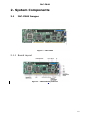
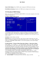
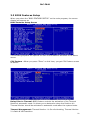
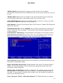
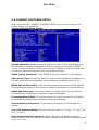
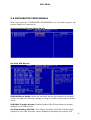
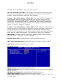
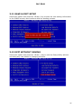
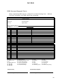
IAC-F848 Manual IAC-F848 IAC-F848 Manual © Copyright 2007, Lanner Electronics, Inc. All rights reserved. This document contains proprietary information that is protected by copyright. No part of this document may be reproduced, transmitted, transcribed, stored in a retrieval system, or translated into any language in any form by any means without the written express of Lanner Electronics, Inc. The author and Lanner Electronics, Inc. have used their best efforts in preparing this manual. However, the author and Lanner Electronics, Inc. make no warranties of any kind, expressed or implied, with regard to the informational content, documentation, or files contained in this manual, and shall not be liable for technical or editorial errors or omissions contained herein. In no event shall the author or publisher be responsible or liable for any incidental or consequential damages resulting from the furnishing, performance, or use of this material. TRADEMARKS Internet Explorer, Windows Explorer, and Windows are trademarks or registered trademarks of Microsoft Corporation. Other products mentioned herein may be trademarks/or registered trademarks of their respective owners. 2 IAC-F848 Safety Guidelines Follow these guidelines to ensure general safety: Keep the chassis area clear and dust-free during and after installation. Do not wear loose clothing or jewelry that could get caught in the chassis. Fasten your tie or scarf and roll up your sleeves. Wear safety glasses if you are working under any conditions that might be hazardous to your eyes. Do not perform any action that creates a potential hazard to people or makes the equipment unsafe. Disconnect all power by turning off the power and unplugging the power cord before installing or removing a chassis or working near power supplies Do not work alone if potentially hazardous conditions exist. Never assume that power is disconnected from a circuit; always check the circuit. Operating Safety Electrical equipment generates heat. Ambient air temperature may not be adequate to cool equipment to acceptable operating temperatures without adequate circulation. Be sure that the room in which you choose to operate your system has adequate air circulation. Ensure that the chassis cover is secure. The chassis design allows cooling air to circulate effectively. An open chassis permits air leaks, which may interrupt and redirect the flow of cooling air from internal components. Electrostatic discharge (ESD) can damage equipment and impair electrical circuitry. ESD damage occurs when electronic components are improperly handled and can result in complete or intermittent failures. Be sure to follow ESD-prevention procedures when removing and replacing components to avoid these problems. Wear an ESD-preventive wrist strap, ensuring that it makes good skin contact. If no wrist strap is available, ground yourself by touching the metal part of the chassis. Periodically check the resistance value of the antistatic strap, which should be between 1 and 10 megohms (Mohms). 3 IAC-F848 EMC Notice This equipment has been tested and found to comply with the limits for a Class A digital device, pursuant to Part 15 of the FCC Rules. These limits are designed to provide reasonable protection against harmful interference when the equipment is operated in a commercial environment. This equipment generates, uses, and can radiate radio frequency energy and, if not installed and used in accordance with the instruction manual, may cause harmful interference to radio communications. Operation of this equipment in a residential area is likely to cause harmful interference in which case users will be required to correct the interference at their own expense. Class A Notice for FCC Modifying the equipment without the authorization of Lanner Electronics, Inc. may result in the equipment no longer complying with FCC requirements for Class A digital devices. In that event, your right to use the equipment may be limited by FCC regulations, and you may be required to correct any interference to radio or television communications at your own expense. This equipment is in compliance with the essential requirements and other relevant provisions of Directive 1999/5/EC. 4 IAC-F848 Contents Safety Guidelines....................................................................... 3 EMC Notice................................................................................. 4 Contents..................................................................................... 5 1. Product Overview.................................................................. 7 1.1 Product Introduction................................................................7 1.2Features and Benefits...............................................................7 1.3Specifications..........................................................................8 1.4 Package Contents...................................................................9 1.5 Technical Assistance................................................................9 2. System Components.............................................................10 2.1 IAC-F848 Images...................................................................10 2.1.1 Board Layout......................................................................10 2.1.2 Dimensions (mm)................................................................11 2.2 Settings and I/O Connectors....................................................11 CCMOS2: Clear CMOS Data ..........................................................11 COMA1: Pin header......................................................................11 COMB1: Pin header......................................................................11 FDC A1: Floppy Interface Connector (34 Pin Header)........................12 LAN B1: LAN CONNECTOR. ...........................................................12 USB F1-F4:USB Port #1-#4.........................................................12 ATX C1: For ATX Function.............................................................13 ATX PWR1: ATX 4 PIN CONNECTOR (FOR +12V VCORE)...................13 FPIO1: 4-Pin Power AND RESET FUNCTION.....................................13 LPT A1:Parallel Connector (26 Pin 2.54mm Pitch Header)................13 IRDA1: IRDA1 Connector..............................................................14 CPU FAN1: 4 Pin FAN Connector.....................................................14 VGA1: External VGA Connector (12 Pin Header)...............................14 IDE1: IDE Interface Connector......................................................14 CN1: Compact Flash Connector.....................................................15 PCI B1: MINI PCI Connector..........................................................15 SATA1-SATA4 (SATA Connector)....................................................16 3. BIOS Setup...........................................................................18 3.1 Main Program Screen. . ...........................................................19 3.2 Standard CMOS Setup. ...........................................................20 3.3 BIOS Features Setup..............................................................22 3.4 CHIPSET FEATURES SETUP......................................................25 3.5 INTEGRATED PERIPHERALS.....................................................27 3.6 POWER MANAGEMENT SETUP..................................................29 3.7 PNP/PCI CONFIGURATION.......................................................32 3.8 PC HEALTH STATUS................................................................33 3.9 LOAD OPTIMIZED DEFAULTS....................................................34 3.10 SET SUPERVISOR / USER PASSWORD.....................................34 3.11 SAVE & EXIT SETUP..............................................................36 3.12 EXIT WITHOUT SAVING.........................................................36 Terms and Conditions...............................................................37 Warranty Policy ..........................................................................37 5 IAC-F848 RMA Service . .............................................................................37 Requesting a RMA#.....................................................................37 RMA Service Request Form. ..........................................................38 6 IAC-F848 1. Product Overview 1.1 Product Introduction IAC-F848 is a full-size PICMG 1.0 compliant SBC supporting an Intel Pentium 4 LGA775 processor. Built around the Intel 945G + ICH7 Chipset, the IAC-F848 offers a multitude of advanced connectivity features such as VGA / SATA / LAN / USB / CF / Mini-PCI and optional with Second LAN / Audio / LVDS / DVI / TV-Out / S-Video. 1.2 • Features and Benefits Supports Intel Pentium 4 and Pentium D, LGA775 CPU • Intel 82945G chipset with FSB 533/800/1066MHz supports HyperThreading Technology • Two DIMM up to 2GB DDR2 400/533/667, Non-ECC SDRAM • Option Audio/LCD/DVI/TV-Out/S-Video • Dual Intel 82573L 10/100/1000Mbps LAN • Type I/II CF, Mini-PCI socket • PICMG 1.0 Compliant 7 IAC-F848 1.3 Specifications FEATURE Platform Sy stem Memory Storage Interface Networking DESCRIPTION Form Factor Full-size, PICMG 1.0 Processor Supports LGA775 Intel Pentium 4, Pentium D with 533/800/1066MHz FSB Chipset Intel® 82945G / 82801GB ICH7R BIOS Award Flash BIOS Cache Memory Processor Built-in Technology DDR2 400/533/667 SDRAM, Dual-Channel Max Capacity 2GB Socket 240-pin DIMM x2 Hard Drive Interface IDE x1, Serial ATA II x4 SSD (CF Socket) CompactFlash I/II x1 Speed 10/100/1000 Mbps I/O RJ45 x1 , Option RJ45 x1 on Braccket Controller Intel 82573L Controller Intel® 82945G GMCH integrated Graphic Media Accelerator 950 built-in high quality 2D/3D engine and High definition streams for MPEG playback Shared memory DVMT(UMA )mode, 1MB/8MB of memory Pre-allocated Output VGA, optional DVI, LVDS and TV-out Codec Realtek ALC203 AC97 audio codec I/O Floppy Drive Interface Serial Port Mic-in, Line-in, Speaker-out via add on bracket Module Parallel Port LPT Pin Header 2.54mm x 1 Universal Serial Bus 8 (v 2.0) Serial-ATA 4 Digital I/O 4bit Digital I/O with pin-header (4 in/4 out) Bus interface PCI /ISA IR Interface 115k bps, IrDA 1.0 compliant with pin-header connector Keyboard Mini-DIN PS/2 Mouse Mini-DIN PS/2 Controller iTE8712F-S Super I/O including CPU temperature, Voltage and FAN Monitoring RTC RTC with Li-Battery Watchdog timer 256-level time-out intervals Display Audio I/O Interface Hardware Monitoring FDD header 2.0mm x 1 RS-232 x3, RS-232/422/485 x1 Cooling Heatsink & Fan Expansion Mini-PCI x1 Temperature, ambient operating Environmental Humidity (RH), Parameters ambient operating 0~60°C (32~140°F) 5~95% relative humidity, non-condensing Storage Temperature -20~70°C (-4~158°F) Physical Dimensions Power Compliance Dimensions 338x122mm (13.3” x 4.8”) Input +12V ,+5V,-12V power input Form Factor AT/ATX support CE, FCC, RoHS 8 IAC-F848 1.4 Package Contents Item Q'ty Description IAC-F848 Series SBC 1pcs Single Board Computer LPT/COM Cable 1pcs 216C3 Cable (LPT&COM Bracket) 29cm ATX Feature Cable 1pcs 4-Pin Cable 40cm FDD Cable 1pcs 34-to-34Pin Cable 50cm IDE Cable 1pcs ATA100 40-Pin IDE with Key SATA Cable 2pcs 7-Pin 15cm PS/2 Cable 1pcs PS/2 Y Cable 5-Pin 13.5cm USB Cable 2pcs USB Cable/Bracket 2-Ports CD 1pcs CD V1.0 For IAC-F848 Driver and Manual 1.5 Technical Assistance Should you have any questions or problems with your product, please contact the Lanner sales team. Phone: 886-2-8692-6060 Fax: 886-2-8692-6101 E-mail: sales@lannerinc.com Prior to contacting us, we ask that you first check the electronic product documentation for assistance. Should you still have questions, we recommend you have the following information on hand in order to expedite the process: 1. IAC-F848 model name 2. Part number 3. Abnormal behavior and/or error messages reported by your network system 4. Your questions or a description of the problem you are experiencing 9 IAC-F848 2. System Components 2.1 IAC-F848 Images Figure 1 – IAC-F848 2.1.1 Board Layout Figure 2 – IAC-F848 Key Features 10 IAC-F848 2.1.2 Dimensions (mm) Figure 3 – Dimensions 2.2 Settings and I/O Connectors The jumper settings and I/O connectors of the IAC-F848 board are specific to the IAC-F848. Changing these settings may result in malfunctions or damage to your system. CCMOS2: Clear CMOS Data DESCRIPTION CMOS Normal (Default) 1-2 Clear CMOS 2-3 COMA1: Pin header PIN NO. DESCRIPTION PIN NO. DESCRIPTION 1 NDCDA# 2 NSINA 3 NSOUTA 4 NDTRA# 5 GND 6 NDSRA# 7 NRTSA# 8 NCTSA# 9 NRIA# 10 NC COMB1: Pin header PIN NO. DESCRIPTION PIN NO. DESCRIPTION 1 COMB1 2 NDSRB# 3 COMB2 4 NRTSB# 5 COMB3 6 NCTSB# 7 COMB4 8 NRIB# 9 GND 10 NC 11 IAC-F848 PK M1: PS/2 Keyboard & Mouse Connector PIN NO. DESCRIPTION PIN NO. DESCRIPTION 1 KBDT 2 MSDT 3 GND 4 +KBMS 5 KBCK 6 MSCK FDC A1: Floppy Interface Connector (34 Pin Header) PIN NO. DESCRIPTION PIN NO. DESCRIPTION 1 Ground 2 Density Select 3 Ground 4 NC 5 Ground 6 DS1 7 Ground 8 Index # 9 Ground 10 Motor Enable A # 11 Ground 12 Drive Select B # 13 Ground 14 Drive Select A # 15 Ground 16 Motor Enable B # 17 Ground 18 Direction # 19 Ground 20 Step # 21 Ground 22 Write Data # 23 Ground 24 Write Gate # 25 Ground 26 Track 0 # 27 Ground 28 Write Protect # 29 NC 30 Read Data # 31 Ground 32 Head Side Select # 33 NC 34 Disk Change # LAN B1: LAN CONNECTOR PIN NO. DESCRIPTION PIN NO. DESCRIPTION 1 PE_MMIP0_0 2 PE_MMIN0_0 3 PE_MMIP1_0 4 PE_MMIP2_0 5 PE_MMIN2_0 6 PE_MMIN1_0 7 PE_MMIP3_0 8 PE_MMIN3_0 9 LINK100A_N 10 LINK1GA_N 11 ACTA_N 12 P3V3 USB F1-F4:USB Port #1-#4 PIN DESCRIPTION PIN DESCRIPTION 1 USB_VCC 2 GND 3 NC 4 USB_TP 5 USB_TN 6 USB_TN 7 USB_TP 8 NC 9 GND 10 USB_VCC 2 10 1 9 12 IAC-F848 ATX C1: For ATX Function PIN DESCRIPTION 1 GND 2 5VSB 3 GND 4 PS_ON# ATX PWR1: ATX 4 PIN CONNECTOR (FOR +12V VCORE) PIN DESCRIPTION PIN DESCRIPTION 1 GND 2 GND 3 +12V_CORE 4 +12V_CORE FPIO1: 4-Pin Power AND RESET FUNCTION PIN NO. DESCRIPTION 1 5VSB 2 GND 3 FP_SWIN 4 GND 5 RESET 2-3(POWER BUTTOM) 4-5(RESET) LPT A1:Parallel Connector (26 Pin 2.54mm Pitch Header) PIN NO. DESCRIPTION PIN NO. DESCRIPTION 1 Strobe # 2 Auto Form Feed 3 Data0 4 Error # 5 Data1 6 Initialize # 7 Data2 8 Printer Select IN # 9 Data3 10 round 11 Data4 12 Ground 13 Data5 14 Ground 15 Data6 16 Ground 17 Data7 18 Ground 19 Acknowledge # 20 Ground 21 Busy 22 Ground 23 Paper Empty 24 Ground 25 Printer Select 26 KEY 13 IAC-F848 IRDA1: IRDA1 Connector PIN NO. DESCRIPTION 1 VCC 2 NC 3 IRRX 4 GND 5 IRTX CPU FAN1: 4 Pin FAN Connector PIN NO. DESCRIPTION 1 Ground 2 +12V 3 FAN Status 4 NC VGA1: External VGA Connector (12 Pin Header) PIN NO. DESCRIPTION PIN NO. DESCRIPTION 1 R 2 G 3 B 4 NC 5 GND 6 GND 7 GND 8 GND 9 NC 10 GND 11 NC 12 VGADDCDATA 13 H_SYNC 14 V_SYNC 15 VGADDCCLK IDE1: IDE Interface Connector PIN NO. DESCRIPTION PIN NO. DESCRIPTION 1 Reset # 2 Ground 3 Data 7 4 Data 8 5 Data 6 6 Data 9 7 Data 5 8 Data 10 9 Data 4 10 Data 11 11 Data 3 12 Data 12 13 Data 2 14 Data 13 15 Data 1 16 Data 14 17 Data 0 18 Data 15 19 Ground 20 KEY 21 DMA REQ# 22 Ground 23 IOW # 24 Ground 25 IOR # 26 Ground 27 IOCHRDY 28 Ground 29 DMA ACK # 30 Ground 31 Interrupt 32 NC 33 SA1 34 PD80P / SD80P 35 SA0 36 SA2 14 IAC-F848 37 HDC CS0 # 38 HDC CS1 # 39 HDD Active LED # 40 Ground CN1: Compact Flash Connector PIN DESCRIPTION PIN DESCRIPTION 1 GND 26 CD1- 2 DATA3 27 DATA11 3 DATA4 28 DATA12 4 DATA5 29 DATA13 5 DATA6 30 DATA14 6 DATA7 31 DATA15 7 CE1# 32 CE2# 8 A10 33 VS1# 9 OE# 34 IOR# 10 A9 35 IOW# 11 A8 36 WE# 12 A7 37 READY# 13 CFVCC3 38 CFVCC3 14 A6 39 CSEL 15 A5 40 VS2# 16 A4 41 RESET 17 A3 42 WAIT# 18 A2 43 INPACK# 19 A1 44 REG# 20 A0 45 DASP# 21 DATA0 46 DIAG# 22 DATA1 47 DATA8 23 DATA2 48 DATA9 24 WP 49 DATA10 25 CD2- 50 GND PCI B1: MINI PCI Connector PIN NO. DESCRIPTION PIN NO. DESCRIPTION 1 TIP 2 RING 3 8PMJ-3 4 8PMJ-1 5 8PMJ-6 6 8PMJ-2 7 8PMJ-7 8 8PMJ-4 9 8PMJ-8 10 8PMJ-5 11 LED1_GRNP 12 LED2_YELP 13 LED1_GRNN 14 LED2_YELP 15 CHSGND 16 RESERVED 17 INT-B 18 +5V 19 +3.3V 20 INT-A 21 RESERVED 22 RESERVED 23 GROUND 24 3.3VAUX 25 CLK 26 RST 27 GROUND 28 +3.3V 29 REO 30 GNT 15 IAC-F848 31 +3.3V 32 GROUND 33 AD31 34 PME 35 AD29 36 RESERVED 37 GROUND 38 AD30 39 AD27 40 +3.3V 41 AD25 42 AD28 43 RESERVED 44 AD26 45 C_BE-3 46 AD24 47 AD23 48 IDSEL 49 GROUND 50 GROUND 51 AD21 52 AD22 53 AD19 54 AD20 55 GROUND 56 PAR 57 AD17 58 AD18 59 C_BE-2 60 AD16 61 IRDY 62 GROUND 63 +3.3V 64 FRAME 65 CLKRUN 66 TRDY 67 SERR 68 STOP 69 GROUND 70 +3.3V 71 PERR 72 DEVSEL 73 C_BE-1 74 GROUND 75 AD14 76 AD15 77 GROUND 78 AD13 79 AD12 80 AD11 81 AD10 82 GROUND 83 GROUND 84 AD9 85 AD8 86 C_BE-0 87 AD7 88 +3.3V 89 +3.3V 90 AD6 91 AD5 92 AD4 93 RESERVED 94 AD2 95 AD3 96 AD0 97 +5V 98 RESERVED-WIP 99 AD1 100 RESERVED-WIP 101 GROUND 102 GROUND 103 AC_SYNC 104 M66EN 105 AC_SDATA_IN 106 AC_SDATA_OUT 107 AC_BIT_CLK 108 AC_CODEC_ID0 109 AC_CODEC_ID1 110 AC_RESET 111 MOD_AUDIO_MON 112 RESERVED 113 AUDIO_GND 114 GROUND 115 SYS_AUDIO_OUT 116 SYS_AUDIO_IN 117 SYS_AUDIO_OUT GND 118 SYS_AUDIO_IN GND 119 AUDIO_GND 120 AUDIO_GND 121 RESERVED 122 MPCIACT 123 VCC5VA 124 3.3AUX SATA1-SATA4 (SATA Connector) PIN NO. 1 DESCRIPTION GND PIN NO. DESCRIPTION 2 SATA_TXP 3 SATA_TXN 4 5 SATA_RXN 6 7 GND 8 GND SATA_RXP GND 16 IAC-F848 9 GND 17 IAC-F848 3. BIOS Setup BIOS Setup Award‘s ROM BIOS provides a built-in Setup program that allows users to modify the basic system configuration and settings. The modified data will be stored in a battery-backed CMOS RAM so that this data will be retained even when the power is turned off. In general, the information saved in the CMOS RAM remains unchanged unless there is a configuration change in the system, such as hard drive replacement or new equipment installment. Running AWARD BIOS The Setup Utility is stored in the BIOS ROM. When the power of the computer system is turned on, a screen message will appear to give you an opportunity to call up the Setup Utility while the BIOS will enter the Power On Self Test (POST) routines. The POST routines perform various diagnostic checks while initializing the board hardware. If the routines encounter an error during the tests, the error will be reported in one of two ways, a series of short beeps or an error message on the screen. There are two kinds of errors, fatal and non-fatal. The system can usually continue the boot up sequence with non-fatal errors. Non-fatal error messages usually appear on the screen along with the following instructions: “ Press <F1> to RESUME ” Write down the message and press the F1 key to continue the boot up sequence. After the POST routines are completed, the following message appears: “ Press DEL to enter SETUP ” Entering Setup Turn on the power of the computer system and press <Del> immediately. If you don’t have the chance to respond, reset the system by simultaneously pressing the <Ctrl>, <Alt> and <Delete> keys, or by pushing the ‘ Reset ’ button on the system cabinet. You can also restart by turning the system OFF then ON. CMOS Setup Utility To access the AWARD BIOS SETUP program, press the <DEL> key. The screen display will appears as shown below: 18 IAC-F848 3.1 Main Program Screen This screen provides access to the utility‘s various functions. Listed below is explanation of the keys displayed at the bottom of the screen: <ESC>: Exit the utility. <↑↓→ ←>: Use arrow keys↑↓→ ← to move cursor to your desired selection. <F1> : General Help <F10>: Saves all changes made to Setup and exits program. Standard CMOS Setup: Use this menu for basic system configurations. Advanced BIOS Features: Use this menu to set the Advanced Features available on your system. Advanced Chipset Features: Use this menu to change the values in the chipset registers and optimizes your system’s performance. Integrated Peripherals: Use this menu to specify your settings for integrated peripherals. Power Management Setup: Use this Menu to specify your settings for power management. PnP/PCI Configurations: This entry appears if your system supports PnP/PCI. PC Health Status: This entry shows your PC health status. If Hardware Monitor Chipset is installed. Load Optimized Defaults: Use this menu to load the BIOS default values that are factory settings for optimal performance system operations. Set Supervisor Password: Use this menu to set Supervisor Passwords. Set User Password: Use this menu to set User Passwords. 19 IAC-F848 Save & Exit Setup: Save CMOS value changes to CMOS and exit setup. Exit Without Saving: Abandon all CMOS value changes and exit setup. 3.2 Standard CMOS Setup When you select the “STANDARD CMOS SETUP” on the main program, the screen display will appears as: Standard CMOS Setup Screen The Standard CMOS Setup utility is used to configure the following components such as date, time, hard disk drive, floppy drive, display and memory. Once a field is highlighted, on-line help information is displayed in the left bottom of the Menu screen. Set Date: Month, Date, and Year. Set Time: Hour, Minute and Second. Use 24-hour clock format (for p.m. time, add 12 to the hour number, e.g. you would enter 4:30 p.m. as 16:30). When you select the “STANDARD CMOS SETUP” on the main program, the screen display will appears as: Primary Master / Primary Slave Secondary Master / Secondary Slave: Press PgUp / <+> or PgDn / <-> to select Manual, None, Auto type. Note that the specifications of your drive must match with the drive table. The hard disk will not work properly if you enter improper information for this category. If your hard disk drive type is not matched or listed, you can use Manual to define your own drive type manually. If you select Manual, related information is asked to be entered to the following items. Enter the information directly from the keyboard. This information should be provided in the documentation from your hard disk vendor or the system manufacturer. If the controller of HDD interface is SCSI, the selection shall be “None” If the controller of HDD interface is CD-ROM, the selection shall be “None” Here is a brief explanation of drive specifications: Access Mode: The settings are Auto, Normal, Large, and LBA. 20 IAC-F848 Cylinder: Number of cylinders Head: Number of heads Precomp: Write precom Landing Zone: Landing Zone Sector: Number of sectors Drive A and Drive B: Select the correct specifications for the diskette drive(s) installed in the computer. Note: 1. Not Installed could be used as an option for diskless workstations. 2. Highlight the listing after each drive name and select the appropriate entry. Halt On: During the power-on-self-test (POST), the computer stops if the BIOS detect a hardware error. You can tell the BIOS to ignore certain errors POST and continue the boot-up process. These are the selections: 21 IAC-F848 3.3 BIOS Features Setup When you select the “BIOS FEATURES SETUP” on the main program, the screen display will appear as: BIOS Features Setup Screen The following explains the options for each of the features as listed in the above menu: CPU Feature : When you press “Enter” on this item, you get CPU Feature screen as below: Delay Prior to Thermal: BIOS feature controls the activation of the Thermal Monitor's automatic mode. It allows you to determine when the Pentium 4's Thermal Monitor should be activated in automatic mode after the system boots. Thermal Management: Thermal Monitor 1 is On-die throtting, Thermal Monitor 2 is Ratio & VID transition. 22 IAC-F848 TM2 Bus Ratio: Represents the frequency (bus ratio)'of the throttled performance state that will be initiated when the on-die sensor gose from not hot to hot. TM2 Bus VID: Represents the voltage of the throttled performance state that will be initiated when the on-die sensor gose from not hot to hot. Limit CPUID Maxval: Enable Limit CPUID Maximum value to 3 when use older OS like NT4. Disable CPUID Limit for windows XP. C1E Function: Enable CPU Enhanced Halt (C1E) function. Disable CPU Enhanced Halt (C1E) function. Execute Disable Bit : When enabled, the processor prevents the execution of code in data-only memory pages. This provides some protection against buffer overflow attacks Virtualization Technology : Enable/Disable Virtualization technology function. Hard disk boot priority: When press enter, then will display screen as below: Select boot sequence for onboard(or add-on cards) SCSI, RAID, etc. Virus warning: Enable/Disable anti-virus protection by monitoring writes to the boot sector and partition table. Hyper-Threading Technology: Enable/Disable CPU Hyper Threading Feature. Please note that this feature is only working for operating system with multi processors mode supported. Quick Power On Self Test: Setting is “Enabled”. This speeds up the Power On Self Test (POST) by skipping some items that are normally checked during the full POST. If your system is functioning normally, you can choose this feature to speed up the booting process. First / Second / Third / Other Boot Device: The BIOS attempts to load the 23 IAC-F848 operating system from the devices in the sequence selected in these items. The settings are Floppy, LS/ZIP, HDD-0/HDD-1/HDD-2/HDD-3, SCSI, CDROM, LAN, and Disabled Boot Up Floppy Seek: The defaults setting is “Disabled”. When enabled, the BIOS will check whether there is a floppy disk drive installed. Boot Up NumLock Status: The default setting is “On”. If it set “Off”, the cursor controls will function on the numeric keypad. Typematic Rate Setting: The default setting is “Disabled”. If enabled, you can set the typematic rate and typematic delay. Typematic Rate (Chars/Sec) : This setting controls the speed at which the system registers the repeated keystrokes. The choices range from 6 to 30 Chars/Sec. The default setting is “6” Chars/Sec. Typematic Delay (M/Sec) : This setting controls the time between the display of the first and second characters. There are four delay choices: 250ms, 500ms, 750ms and 1000ms. The default setting is “250” ms. Security Option: This setting controls the password in the main screen. The options are “Setup” and “System”. Select “Setup” and it will protect the Setup Utility settings from being tampered with. Select “System” if you want to use password feature every time the system boots up. The default setting is “Setup”. You can create your password by using the “SUPERVISOR/USER PASSWORD” utility on the main program screen. APIC Mode: Enable/Disable APIC Mode. The APIC provides multiprocessor support, more IRQs and faster interrupt handling. MPS Version Control For OS: MPS 1.1 was the original specification. MPS version 1.4 adds extended configuration tables for improved support of multiple PCI bus configurations and greater expandability in the future. In addition, MPS 1.4 introduces support for a secondary PCI bus without requiring a PCI bridge. Full Screen Logo show: Enable/Disable display the full-screen logo during the boot-up sequence. 24 IAC-F848 3.4 CHIPSET FEATURES SETUP When you select the “CHIPSET FEATURES SETUP” on the main program, the screen display will appears as: Chipset Features Setup Screen Spread Spectrum: Enable/Disable to reduce the EMI of your motherboard by modulating the signals it generates so that the spikes are reduced to flatter curves. It achieves this by varying the frequency slightly so that the signal does not use any particular frequency for more than a moment DRAM Timing Selectable: To set DRAM Timing by SPD(auto) or by Manual. CAS latency Time: Control the delay (in clock cycles) between the assertion of the CAS signal and the availability of the data from the target memory cell. DRAM RAS-to-CAS Delay: to set the delay between the RAS and CAS signals. The appropriate delay for your memory module is reflected in its rated timings. DRAM RAS Precharge: To set the number of cycles required for the RAS to accumulate its charge before another row can be activated. Precharge Delay(TRAS): To set the number of cycles required for the RAS to accumulate its charge before another row can be activated. System Memory Frequency: To set Memory frequency by AUTO detect or manual. SLP_S4# Assertion Width: Set SLP_S4# pin width to “1-2 sec”, ”2-3 sec”,”3-4 sec”, “4-5 sec”. PCI Express Root Port Function: Press Enter then will display screen as below: Control PCIE Port as Auto, Enable or Disable. And PCI-E Compliancy Mode to V1.0 or 1.0A. 25 IAC-F848 PEG Force X1: Enable/Disable the PCI Express X16 slot will be forced to run in the PCI Express X1 mode On-Chip Frame Buffer Size: Control the amount of system memory that is allocated to the integrated graphics processor when the system boots up. DVMT Mode: Intel's Dynamic Video Memory Technology (DVMT) takes that concept further by allowing the system to dynamically allocate memory resources according to the demands of the system at any point in time. When set to Fixed, the graphics driver will reserve a fixed portion of the system memory as graphics memory. When set to DVMT, the graphics chip will dynamically allocate system memory as graphics memory, according to system and graphics requirements. When set to Both, the graphics driver will allocate a fixed amount of memory as dedicated graphics memory, as well as allow more system memory to be dynamically allocated between the graphics processor and the operating system. DVMT/FIXED Memory size: It allows to set the maximum amount of system memory that can be allocated as graphics memory, but only for the Fixed or DVMT operating modes. When the DVMT + Fixed mode is selected, this BIOS feature is grayed out because when in that operating mode, the graphics driver automatically allocates a total of 128MB of graphics memory. Boot Display: Boot device by CRT or Panel or TV or etc. Panel Number: Please select the type of panel you are incorporating with our single board computer. Consult your panel manual for detail information. TV Standard: Setting this correctly allows the video encoder to produce the correct analog video output for your television set Video Connector: Select Video connector type. TV Format: Select TV format type. 26 IAC-F848 3.5 INTEGRATED PERIPHERALS When you select the “INTEGRATED PERIPHERIALS” on the main program, the screen display will appears as: Integrated Peripherals Setup Screen On-Chip IDE Device: IDE HDD Block Mode: Speed up hard disk access by transferring multiple sectors of data per interrupt instead of using the usual single-sector transfer mode. IDE DMA Transfer Access: Enable/Disable DMA (Direct Memory Access) support for all IDE devices. On-Chip Primary PCI IDE : The chipset contains a PCI IDE interface with support for two IDE channels. Select Enabled to activate the primary IDE 27 IAC-F848 interface. Select Disabled to deactivate this interface. On-Chip Secondary PCI IDE : The chipset contains a PCI IDE interface with support for two IDE channels. Select Enabled to activate the secondary IDE interface. Select Disabled to deactivate this interface. Primary / Secondary Master / Slave PIO : The four IDE PIO (Programmed Input/Output) fields let you set a PIO mode (0-4) for each of the four IDE devices that the onboard IDE interface supports. Modes 0 through 4 provide successively increased performance. In Auto mode, the system automatically determines the best mode for each device. The settings are “Auto”, “Mode 0”, “Mode 1”, “Mode 2”, “Mode 3”, “Mode 4”. Primary / Secondary Master / Slave UMDA : Ultra DMA/66 implementation is possible only if your IDE hard drive supports it and the operating environment includes a DMA driver (Windows 98 OSR2 or a third-party IDE bus master driver). If your hard drive and your system software both support Ultra DMA/66, select Auto to enable BIOS support. The settings are “Auto” and “Disabled”. SATA Mode: Controls the SATA controller's operating mode. There are three available modes - IDE, SATA or AHCI and RAID. On-Chip Serial ATA: Enable/Disable on chip serial ATA controller. SATA Port Speed Settings: Select SATA speed to Disable or GEN I/ GEN II. PATA Mode : Select PATA to Primary or Slave. On Board Device: USB Controller: Enable/Disable USB controller. USB 2.0 Controller: You can disable this function if you are not using onboard USB 2.0 feature. USB Keyboard Support: Enable/Disable USB keyboard support. USB Mouse Support: Enable/Disable USB mouse support. Azalia /AC97 Audio select: Select Audio Mode is Azalia or AC97. You also can by AOTO detect. 28 IAC-F848 Super IO Device: Onboard FDD Controller : Select Enabled if your system has a floppy disk controller (FDC) installed on the system board and you want to use it. If you install add-in FDC or the system has no floppy drive, select Disabled in this field. The settings are “Enabled” and “Disabled”. Onboard Serial Port 1 / Port 2 : Select an address and corresponding interrupt for the first and second serial ports. The settings are “3F8/IRQ4”, “2E8/IRQ3”, “3E8/IRQ4”, “2F8/IRQ3”, “Disabled”, “Auto”. UART Mode Select : This item allows you to select which mode for the Onboard Serial Port 2. The settings are Normal, IrDA, ASKIR and SCR UR2 Duplex Mode: This item allows you to select the IR half/full duplex function. Onboard Parallel Port : This item allows you to determine onboard parallel port controller I/O address setting. The settings are “378H/IRQ7”, “278H/IRQ5”, “3BC/IRQ7”, “Disabled”. Parallel Port Mode: Select an operating mode for the onboard parallel (printer) port. Select “Normal”, “Compatible”, or “SPP” unless you are certain your hardware and software both support one of the other available modes. ECP Mode Use DMA: Select a DMA channel for the parallel port for use during ECP mode. The settings are “3” and “1”. 3.6 POWER MANAGEMENT SETUP When you select the “POWER MANAGEMENT SETUP” on the main program, the screen display will appears as: Power Management Setup Screen 29 IAC-F848 ACPI Function : This item allows you to enable or disable the Advanced Configuration and Power Management (ACPI). ACPI Suspend Type: You can select Suspend type to S1 or S3. S1is Power On Suspend. S3(STR) is Suspend To RAM. Run VGABIOS if S3 Resume: This item allows invoke VGA bios when resume from S3. Power Management: This option allows you to select the type (or degree) of power saving for Doze, Standby, and Suspend modes. Video Off Method : This determines the manner in which the monitor is blanked.. This specifies the power saving state that the VGA video subsystem enters after the specified period of display inactivity has expired. Blank Screen: The BIOS will only black the screen when the system gets into power management mode and writes blanks to the video buffer. V/H SYNC + Blank: Writes blanks to the video buffer, and turns off the vertical and horizontal scanning. 30 IAC-F848 DPMS: Allows the BIOS to control the video display card if it supports the DPMS feature. Video Off in suspend : Enable/Disable Video Off in suspend. Suspend Type: To select suspend type as “Stop Grant” or “PwrOn Suspend”. MODEM Use IRQ : Name the interrupt request (IRQ) line assigned to the modem (if any) on your system. Activity of the selected IRQ always awakens the system. Suspend Mode: This field specifies the length of time of system inactivity while in full power on state before the computer enters suspend mode and motivates the enable 'Wake Up Events In Doze & Standby' / 'PM Events'. HDD Power down: When enable and after the set time of system inactivity, the hard disk drive will be powered down while all other devices remain active. Soft-Off by PWRBTN: This field defines the power off mode when using an ATX power supply. Instant Off: Allows power off immediately upon pressing the power button. Delay 4 sec: the system powers off when the power button is pressed for more than four seconds or enters the suspend mode when pressed for less than four seconds. Wake-Up by PCI card: Enable/Disable PCI PME wake up function. Power On By Ring: Enable/Disable Power On By Ring function. USB KB Wake-Up From S3: Enable/Disable wakeup by USB KB function. Resume By Alarm: This field enables the user to set the option to enable an RTC Alarm (real time clock) to wake up the computer system from power saving mode. When this option is enabled another field allowing the user to set the alarm time on, appears. The additional field has options for date, hour, minute and second. PWRON After PWR-Fail: When power fail, you can select power ON or Off or Former status. Reload Global Timer Events: When any of these options are enabled or set to on, they enable event monitoring on the specified hardware IRQ when the computer is in power saving mode. The computer enters the full power on state if any activity occurs. Those event include LPT , COM, HDD , FDD ,PCI IRQ…etc. Primary IDE 0: Enable/Disable this one of Reload Global Timer Events. Primary IDE 1: Enable/Disable this one of Reload Global Timer Events. Secondary IDE 0: Enable/Disable this one of Reload Global Timer Events. Secondary IDE 1: Enable/Disable this one of Reload Global Timer Events. 31 IAC-F848 FDD,COM,LPT Port: Enable/Disable this one of Reload Global Timer Events. PCI PIRQ[A-D]#: Enable/Disable this one of Reload Global Timer Events. 3.7 PNP/PCI CONFIGURATION Both the ISA and PCI buses on the CPU card use system IRQs & DMAs. You must set up the IRQ and DMA assignments correctly through the PnP/PCI Configuration Setup utility; otherwise the motherboard will not work properly. PnP/PCI Configuration Setup Screen Init Display First: This allows you to select whether display interface (PCI, PCIE, On-Chip graphic...etc. )to boot the system. Reset Configuration Data : Normally, you leave this field “Disabled”, Select “Enabled” to reset Extended System Configuration Data (ESCD) when you exit Setup if you have installed a new add-on and the system reconfiguration has caused such a serious conflict that the operating system cannot boot. The settings are : “Enabled and Disabled”. Resource Controlled By: The Award Plug and Play BIOS has the capacity to automatically configure all of the boot and Plug and Play compatible devices. However, this capability means absolutely nothing unless you are using a Plug and Play operating system such as Windows 98. If you set this field to “Manual” choose specific resources by going into each of the sub menu that follows this field ( a sub menu is proceded by a “►”). The settings are “Auto(ESCD)”, “Manual”. IRQ Resources: When resources are controlled manually, assign each system interrupt as one of the following types, depending on the type of device using the interrupt. 32 IAC-F848 PCI/VGA Palette Snoop : This BIOS feature determines if your graphics card should allow VGA palette snooping by a fixed function display card. Maximum Payload Size: This determines the maximum TLP (Transaction Layer Packet) payload size that can be supported by the motherboard chipset's PCI Express controller. The TLP payload size determines the amount of data transmitted within each data packet 3.8 PC HEALTH STATUS This section helps you to get more information about your system including CPU temperature, FAN speed and voltages. V_CORE, V_ddr, +3.3V, +5V, +12V, Vcc15, Vddr_Vtt, Voltage Battery: Detect system's voltage status automatically. CPU Temp, System Temp: Detect CPU, System temperature automatically. CPUFAN1 Speed, Aux Fan1,2,3 : Detect CPU/ system fan speed status automatically. 33 IAC-F848 3.9 LOAD OPTIMIZED DEFAULTS When you press “Enter” on this item, you get a confirmation dialog box with a message similar to : Load Optimized Defaults (Y/N) ? N Pressing “Y” loads the default values that are factory settings for optimal performance system operations. 3.10 SET SUPERVISOR / USER PASSWORD The “SUPERVISOR/USER PASSWORD” utility sets the password. The SBC is shipped with the password disabled. If you want to change the password, you must first enter the current password, then at the prompt -- enter your new password. The password is case sensitive, and can be up to 8 alphanumeric characters. Press <Enter> after you have finished typing in the password. At the next prompt, confirm the new password by re-typing it and pressing <Enter> again. When you are done, the screen automatically reverts to the main screen. Remember that when you use this feature, the “Security Option” line in BIOS FEATURES SETUP will determine when entering the password will be required. To disable the password, press the <Enter> key instead of entering a new password when the “Enter Password” in the dialog box appears. A message will appear confirming that the password is disabled. If you have set both supervisor and user password, only the supervisor password allows you to enter the BIOS SETUP PROGRAM. Note : If you forget your password, the only way to solve this problem is to discharge the CMOS memory. 34 IAC-F848 35 IAC-F848 3.11 SAVE & EXIT SETUP Select this option and press the <Enter> key to save the new setting information in the CMOS memory and continue with the booting process. 3.12 EXIT WITHOUT SAVING Select this option and press the <Enter > key to exit the Setup Utility without recording any new values or changing old ones. 36 IAC-F848 Terms and Conditions Date:2007.03.19 Warranty Policy 1. All products are under warranty against defects in materials and workmanship for a period of one year from the date of purchase. 2. The buyer will bear the return freight charges for goods returned for repair within the warranty period; whereas the manufacturer will bear the after service freight charges for goods returned to the user. 3. The buyer will pay for repair (for replaced components plus service time) and transportation charges (both ways) for items after the expiration of the warranty period. 4. If the RMA Service Request Form does not meet the stated requirement as listed on “RMA Service,” RMA goods will be returned at customer’s expense. 5. The following conditions are excluded from this warranty: Improper or inadequate maintenance by the customer Unauthorized modification, misuse, or reversed engineering of the product Operation outside of the environmental specifications for the product. RMA Service Requesting a RMA# 1. To obtain a RMA number, simply fill out and fax the “RMA Request Form” to your supplier. 2. The customer is required to fill out the problem code as listed. If your problem is not among the codes listed, please write the symptom description in the remarks box. 3. Ship the defective unit(s) on freight prepaid terms. Use the original packing materials when possible. 4. Mark the RMA# clearly on the box. Note: Customer is responsible for shipping damage(s) resulting from inadequate/loose packing of the defective unit(s). All RMA# are valid for 30 days only; RMA goods received after the effective RMA# period will be rejected. 37 IAC-F848 RMA Service Request Form When requesting RMA service, please fill out the following form. Without this form enclosed, your RMA cannot be processed. Company: Reasons to Return: □ Repair(Please include failure details) □ Testing Purpose Contact Person: Phone No. Purchased Date: Fax No.: Applied Date: RMA No: Return Shipping Address: Shipping by: □ Air Freight □ Sea □ Others:________________ □ Express Item Model Name Item Problem Code Failure Status *Problem Code: 01:D.O.A. 02: Second Time R.M.A. 03: CMOS Data Lost 04: FDC Fail 05: HDC Fail 06: Bad Slot Serial Number 07: 08: 09: 10: 11: 12: BIOS Problem Keyboard Controller Fail Cache RMA Problem Memory Socket Bad Hang Up Software Out Look Damage Request Party Authorized Signature / Date ___ Configuration 13: 14: 15: 16: 17: 18: SCSI LPT Port PS2 LAN COM Port Watchdog Timer 19: 20: 21: 22: 23: 24: DIO Buzzer Shut Down Panel Fail CRT Fail Others (Pls specify) Confirmed By Supplier Authorized Signature / Date 38