1
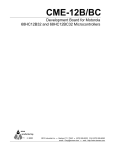
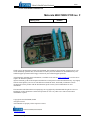
_ V1.0 POD Hardware Reference Motorola 68HC12B32 POD rev. F Ordering code IC20080 Thank you for purchasing this product from iSYSTEM. This product has been carefully crafted to satisfy your needs. Should any questions arise, do not hesitate to contact your local distributor or iSYSTEM directly. Our technical support personnel will be happy to answer all your technical support questions. All information, including contact information, is available on our web site www.isystem.com. Feel free also to explore our alternative products. iSystem constantly yields for development and therefore certain pictures in this documentation may vary slightly from the actual product you received. The differences should be minor, but should you find more serious inconsistencies of the product with the documentation, please contact your local distributor for more information. This document and all documents accompanying it are copyrighted by iSYSTEM and all rights are reserved. Duplication of these documents is allowed for personal use. For every other case a written consent from iSYSTEM is required. Copyright 2001 iSYSTEM, GmbH. All rights reserved. All trademarks are property of their respective owners. www.isystem.com iSYSTEM, August 2001 1/8 _ POD Hardware Reference In-Circuit Emulation PODs The following elements of interest are located on all In-Circuit emulation PODs: • emulation CPU - acts on behalf of target's CPU. On some PODs you must use the same CPU on the POD as it is used on the target (see your POD reference page). In such cases, remove the CPU from the POD and insert the CPU that you use in the target system, in its place. • red LED (D3) - lit when CPU is running • green LED (D4) - lit when Emulator is ready for emulation • a connector, mostly marked ST3 - contains signal lines, some of which are hardware configuration lines (such as bank select signals), others you can use for signal generation (pattern generator outputs). Here are some common signals found on the signal connector, commonly marked as ST3: • GND Ground • BPE External breakpoint input. Active high. • RESO/RO Reset output. Connect to target to reset peripherals. • TRES/TR Target reset input. • AUXn AUX signal inputs (same as inputs on Emulator/trace) Note: On PODs that support synchronization between two or more Emulators (currently only the HC(S)12 Family, see the Synchronization section in the Hardware User's Guide for more information) AUX0 and AUX1 are cut short with Run/Stop synchronization line, and AUX2, AUX3 with RESET synchronization line. You should use these pins to connect to other PODs or target CPUs. • PAT0-2 Pattern generator output on 16-bit POD • OC4-6 Pattern generator output on 8-bit POD Note: The signal connector can also have other markings, like P1, U1, etc. Please refer to the POD-specific documentation for the signal connector name and signals present. iSYSTEM, August 2001 2/8 For every POD the following information is given: • Ordering code. If there are different speed versions of a POD the ordering code is modified by appending the speed in MHz (IC81020-16 for the 16 MHz 8031 POD) • information on available speed versions and required Emulator access time • POD size and position of PIN1 on the target adapter relative to bottom left corner. The memory range specifies the range of addresses that a POD can address. If this specification is omitted the default 1MB is assumed. Note: The In-Circuit Emulator can emulate a processor or a microcontroller. Beside the CPU, additional logic is integrated on the POD. The amount of additional logic depends on the emulated CPU and the type of emulation. A buffer on a data bus is always used (minimal logic) and when rebuilding ports on the POD, maximum logic is used. As soon as a POD is inserted in the target instead of the CPU, electrical and timing characteristics are changed. Different electrical and timing characteristics of used elements on the POD and prolonged lines from the target to the CPU on the POD contribute to different POD characteristics. Consequently, signal cross-talks and reflections occur, capacitance changes, etc. Beside that, pull-up and pull-down resistors are added to some signals. Pull-up/pull-down resistors are required to define the inactive state of signals like reset and interrupt inputs, while the POD is not connected to the target. Because of this, the POD can operate as standalone without the target. Final Target Application Test After the application is being more or less debugged and final application test is performed, it is recommended to remove all breakpoints and to close all debug windows (memory, SFR, watch...) to eliminate any possible influence of the emulator on the CPU execution. There were cases where the target application has been behaving differently with the target CPU inserted or the POD connected. If the debugger is configured to update some debug windows in real-time, the user may not be aware of that the CPU execution may be slightly disturbed. However, when the monitor access type is configured to update debug windows while the CPU is running, the CPU execution is disturbed significantly, depending on the necessary number of memory accesses to update opened debug windows. There are cases when internal peripheral device requires read access of the particular register during the device configuration. The user has had SFR window opened and the necessary read access was actually performed by the debugger and not by the application as it would be correct. Therefore, the application was working fine with the emulator, but a standalone application didn't work correctly, as the peripheral device was not configured properly. iSYSTEM, August 2001 3/8 _ V1.0 POD Hardware Reference Motorola 68HC12 B32 POD rev. F Ordering code IC20080 POD Speed (MHz) 8 Emulator Speed (ns) 65 Exchange CPU YES Before connecting the POD, make sure you have read the technical notes on Motorola 68HC12 Family in the Hardware User's Guide. POD Layout Emulated CPU 68HC912 B32 68HC912 BC32 68HC12BC32 68HC12BE32 iSYSTEM, August 2001 4/8 Jumper Settings On this POD Vcc source and level selection is performed manually through jumper settings. Jumper J2 determines the source: Position Vcc source T Target E Emulator Jumper J2 settings Jumper J1 determines the Vcc level. This setting is ignored if J2 is set to target source. Position Vcc level Set 5.0 V Removed 3.3 V Jumper J1 settings If the internal (Emulator) clock is used and a quartz is used in the target, sometimes the CPU will not start after a reset. In this case the connection between CPU XTAL and the Target XTAL must be broken. The jumper J9 determines this setting. Position Description Set CPU & Target XTAL connected Removed CPU & Target XTAL disconnected Jumper J9 settings Electrical Differences and Rebuilt Ports In general, when emulating the single chip mode, some ports have to be rebuilt on the POD because original ports are used for emulation – typically ports used as address and data bus in extended mode. Special devices, so called port replacement units, provided already by the CPU vendor or other standard integrated circuits are used to rebuilt "lost" ports. Rebuilt ports are logically 100% compatible with original CPU’s ports, but electrical characteristics may differ. If special device (port replacement unit) is available, electrical characteristics don’t differ much and usually the user doesn’t have to pay attention. The differences may become relevant when standard integrated circuits are used and operating close to electrical limits, e.g. when input voltage level is close to specified maximum voltage for low input level (“0”) or specified minimum voltage for high input level (“1”). When emulating the single chip mode, original ports A, B and E are used for the emulation and rebuilt by standard integrated circuits on the POD therefore electrical characteristics are changed. Using the emulator, the port registers (Port Registers and Port Data Direction Registers) belonging to the rebuilt ports must be mapped to the target when emulating the single-chip mode. The rebuilt ports have a 10kOhm pull-up resistor array on the socket. They can be removed if the target application programs these ports as non-pull-up outputs. Port Socket Port A GR7 Port B GR8 Port E GR9 Simulated ports and pull-up resistor sockets iSYSTEM, August 2001 5/8 Whenever operating close to electrical limits and having problems with rebuilt ports please check pull-up and pull-down resistors. They shouldn’t be too strong, neither too weak. Check the voltage level. Try to withdraw from voltage limits. General HC12 Emulation Notes Clock When using the external clock, the HC(S)12 application doesn't start. It works fine when I use internal clock. There are two major issues the user must pay attention to: - Also when using external clock, the user must specify target clock frequency (2*ECLK) in the 'Hardwara/Emulation Options/Vcc/Clock' tab, like in the case when using internal clock. It is required by the debugger to be able to synchronize with on-chip BDM firmware which operates at CPU's system clock frequency. - It is not recommended to use a crystal in the target as a clock source during the emulation. It is recommended that the oscillator is used instead. Normally, a crystal and two capacitors are connected to the CPU's clock inputs in the target application as stated in the CPU datasheets. A length of clock paths is critical and must be taken into consideration when designing the target. During the emulation, the distance between the crystal in the target and the CPU (on the POD) is furthermore increased, therefore the impedance may change in a manner that the crystal doesn't oscillate anymore. In such case, a standalone crystal circuit, oscillating already without the CPU must be built or oscillator used. COP Internal COP must be disabled when using the emulator, respectively while debugging STOP Instruction STOP instruction is completely supported by the emulator. After the STOP instruction is being executed, the CPU is stopped and the debugger displays HALTED status. Note that the debug windows cannot be updated while HALTED status is displayed. When the CPU is awaken either by interrupt or target reset, the emulation/execution proceeds normally. Internal CPU Flash Note that internal FLASH is disabled during the emulation and cannot be used in any way. Internal RAM, Internal EEPROM If the CPU provides a capability to write to the internal RAM or EEPROM via memory window (no specific programming sequence required), the download file can be loaded to the internal RAM or EEPROM using the ‘Target Download’ option. The debugger downloads the code to the internal memory after reset via the CPU. If the CPU requires some registers to be configured before the CPU is able to write into the EEPROM area, the user must configure the necessary registers respectively, using the initialization dialog. Any sequence, added in the initialization dialog, is executed immediately after reset, before the download is performed. Executing the program in the internal RAM or EEPROM has some limitation, depending on the emulation system. The run, stop and single step debug commands can be used in the internal RAM or EEPROM. Note that single step can be performed in the disassembly window , but not in the source window. No breakpoints can be set in the internal memory area. iSYSTEM, August 2001 6/8 Checksum When performing any kind of checksum in the emulated (code) area, note that all breakpoints must be removed before, otherwise the results are distorted. Note that the emulator forces "breakpoint" instruction on the data bus when executing the code at the address where breakpoint is set. Slow Mode It is not recommended to debug the application running in slow mode, due to a CPU flaw. The Signal Connector A signal connector is available on the POD, marked ST3. Pin Signal Signal Description 1 GND Ground 2 GND Ground 3 BPEXT External Breakpoint Input 4 PAT0 Pattern Generator Output 5 TRES Target Reset Input 6 PAT1 Pattern Generator Output 7 RSO Reset Output 8 PAT2 Pattern Generator Output 9 AUX0 AUX Signal Input 10 AUX1 AUX Signal Input 11 AUX2 AUX Signal Input 12 AUX3 AUX Signal Input ST3 Signal Connector Synchronization of Two or More Emulators When multiple emulators should operate synchronously, the synchronization connector marked J4 must be used. All the emulators that should operate synchronously must have connected together (separately) SR (SYNCRESET) pins, SS (SYNC-STOP) pins and GND (ground) pins. Pin Description SS Sync-Stop SR Sync-Reset Synchronization Connector J4 For more information, please refer to the "Synchronization of Two or More Emulators" section of the Hardware User's Guide. Target Adapters iSYSTEM offers various adapter solutions for this POD. Please refer to the adapter documentation for more details. iSYSTEM, August 2001 7/8 POD Target Layout The POD target layout is T_QFP80. 80 78 76 74 72 70 68 66 64 62 79 77 75 73 71 69 67 65 63 61 2 4 6 8 10 12 14 16 18 20 1 3 5 7 9 11 13 15 17 19 59 57 55 53 51 49 47 45 43 41 60 58 56 54 52 50 48 46 44 42 21 23 25 27 29 31 33 35 37 39 22 24 26 28 30 32 34 36 38 40 T_QFP80 – Top POD view T_QFP80 - Dimensions iSYSTEM, August 2001 8/8