1
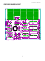
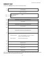
CME12B32 Development Board © Axiom Manufacturing, 1998 717 Lingco Dr., Suite 202 Richardson, TX 75081 972) 994-9676 FAX (972) 994-9170 email: gary@axman.com web: http://www.axman.com C M E 1 2 B 3 2 M A N U A L CONTENTS GETTING STARTED.....................................................................................3 DEVELOPMENT PHILOSOPHY ..................................................................3 TUTORIAL.....................................................................................................4 USING DBUG12..................................................................................................... 4 Example Program................................................................................................ 4 Writing to Internal Flash Memory using AX12..................................................... 5 USING THE BDM..................................................................................................... 6 Example Program................................................................................................ 6 Writing to Internal Flash Memory using the BDM ............................................... 7 CME12B32 BOARD LAYOUT ......................................................................8 MEMORY MAP..............................................................................................9 JUMPERS ...................................................................................................10 MISCELLANEOUS JUMPERS .................................................................................... 10 MOD JUMPERS .................................................................................................... 10 MEM-SEL JUMPERS ............................................................................................ 10 EVU JUMPERS ..................................................................................................... 10 PORTS AND CONNECTORS.....................................................................11 BUS_PORT ........................................................................................................ 11 MCU_PORT1 ..................................................................................................... 11 MCU_PORT2 ..................................................................................................... 12 COM1................................................................................................................. 12 J2 ....................................................................................................................... 12 KEYPAD............................................................................................................. 13 LCD_PORT ........................................................................................................ 13 DEBUG............................................................................................................... 13 TROUBLESHOOTING ................................................................................14 TROUBLESHOOTING STEPS .................................................................................... 14 TIPS AND SUGGESTIONS........................................................................................ 15 AX12 Program................................................................................................... 15 Code Execution.................................................................................................. 15 2 C M E 1 2 B 3 2 GETTING STARTED M A N U A L Thank you for purchasing our CME12B32 development board! The Axiom CME12B32 single board computer is a fully assembled, fully functional development system for the Motorola 68HC12B32 Microcontroller, complete with wall plug style power supply and serial cable. To get started quickly, perform the following test now to make sure everything is working correctly: 1. Create a directory on your PC hard drive for the utility software and copy the contents of the UTL-12B32 disk to that directory. NOTE: it is possible to run the utility software from the floppy disk but not recommended. 2. Connect one end of the supplied 9-pin serial cable to a available COM port on your PC. Connect the other end of the cable to the COM1 port on the CME12B32 board. 3. Apply power to the board by plugging in the power supply that came with the system. 4. Change to the directory containing the utility software and execute the program: AX12.EXE. 5. Select the PC COM Port that you’re using to attach the development board. 6. Select the development board type: CME12-B32. 7. From the main menu select “Terminal Window”. 8. Press then release the RESET button on the CME12B32 board now. 9. If everything is working properly, you should see the monitor prompt in the terminal window. Your board is now ready to use! Press any key to enter the monitor/debugger. If you do not see the monitor/debugger message prompt, or the text is garbage, see the TROUBLESHOOTING section of this manual. DEVELOPMENT PHILOSOPHY Software development on the CME12B32 can be performed using either the DBUG12 monitor utility installed in EPROM (sockets U6/U7), the DBUG12 monitor programmed into the internal Flash EPROM or a Background Debug Module (BDM) connected to the DEBUG connector. Any of these tools can be used to assist in creating and debugging your program that is stored in either internal RAM ($800-$C00) or external RAM (U4/U5 see Memory Map). After satisfactory operation running under a debugger, your program can be written to the Internal Flash Memory by relocating its start address to $8000 and programming it using either the included AX12 program or a BDM. Your program will then run automatically whenever the CME12B32 is powered on or RESET is applied. Option jumpers on the board allow for easy transition from one memory type to another and restoring an operating monitor. 3 C M E 1 2 B 3 2 TUTORIAL M A N U A L This tutorial will walk you thru the complete development cycle of a very simple program. This should help you get started with the specifics of the CME12B32 development process. Be sure to read the rest of this manual as well as the documentation on the disk if you need further information. You can develop software using either your PCs serial port and the DBUG12 monitor utility or your PCs Parallel port and a Background Debug Module (BDM) connected to the DEBUG connector. Using DBUG12 Example Program For this tutorial we’ll use an assembly language program on the UTL12 software disk called HELLO3.ASM. This is a simple program that just sends a text string to your PC serial port using the HC12 SCI0 (COM1) port. You can substitute your own program here if you wish but, to verify everything is working properly, it’s a good idea to start with something simple. 1. If you haven’t done so already, verify that the board is connected and operating properly by following the steps under “GETTING STARTED”. 2. At your PC’s DOS command line prompt, change to your UTL12 software directory. 3. Execute the command: AX12 ↵ This will launch the Axiom programming interface for the HC12 development boards. 4. Select "Assembler" from the main menu and input the file called HELLO3.ASM which is located in the program directory. This will assemble our test source code. 5. If any errors were found, the program listing would be displayed on the screen which contains the errors. Otherwise, you should have the new file HELLO3.S19 (a Motorola hex object file) in your directory. 6. Select “Terminal Window” from the menu. 7. Press and release the RESET button on the board. You should see the monitor prompt. 8. Press any key to start the debugger. 9. Type LOAD ↵ This will prepare the monitor to receive a program. 10. Press the Page Up key and when prompted for a file name, select the file just created called HELLO3.S19 then select [ OK ]. Your program will be sent to internal RAM. 11. Type CALL 900 ↵ This tells the monitor to execute the subroutine at address $900, which is the start of our test program. 12. If everything is working properly you should see the message “Hello World” echoed back to your terminal screen then, since we return at then end of our program, lines containing the internal register status and the monitor prompt. 13. If you didn’t get this message, try going thru this tutorial once more then, if still no go, see the TROUBLESHOOTING section in this manual You can modify the hello program to display other strings or do anything you want. The procedures for assembling your code, uploading it to the board and executing it remain the same. The monitor has many powerful features such as breakpoints, memory dump and modify and program trace. Type HELP at the monitor prompt for a listing of commands available. 4 C M E 1 2 B 3 2 M A N U A L Writing to Internal Flash Memory using AX12 When you’re finished with program development, you will probably want to write your program to Internal Flash Memory so that it executes automatically when you apply power to the board. The following procedure is the easiest way to accomplish this: 1. Use a text editor to modify HELLO3.ASM. You can use the built in “Edit” command in AX12 if you wish. Change the start of your program to program space in the external Flash Memory area ($8000 for example). In the case of HELLO3.ASM, simply comment out the “ORG MONSTRT” line and remove the comment from the “ORG PRGSTRT” line. Also, remove the comment in front of the “LDS #STACK” line, so that our program will initialize the stack (needed when running stand-alone but should not be done while running under the monitor since it must handle the stack). 2. Finally, comment out the “RTS” return line following the “ENDPROG” label. This will allow the program to do an endless loop instead of returning, since we won’t be calling it from the monitor. Save the program and exit the editor. 3. Select “Assembler” from the AX12 menu to assemble the modified HELLO3.ASM program.. This will prompt you for that file name then execute the batch file DO_ASM.BAT which automates the assembly process and creates a listing file. 4. Select “HC12 Utilities” from the menu. Follow ALL the onscreen instructions for executing the utilities firmware. If you have trouble here, see the TROUBLESHOOTING section. 5. From the utilities menu, select "Erase Internal Flash" which must be done before writing over previously programmed memory. 6. Select “Program Internal Flash” and when prompted for a file name, enter the new HELLO3.S19 file then select [OK]. 7. Follow the instructions on screen when finished programming. 8. Remove the MOD jumpers so that the board will reset in single chip mode (auto-start flash memory) 9. Select “Terminal Window” from the menu then cycle power or press RESET on the board. Your new HELLO program should start automatically. WARNING: As a safety precaution, ALWAYS remove the VPP_EN jumper after programming to protect the micro from being accidentally erased or damaged. To return to development mode, simply re-install the MOD jumpers and press RESET. See the Online "Help" menu option for more information and documentation for the other utilities included in AX12. 5 C M E 1 2 B 3 2 M A N U A L Using the BDM If you purchased the BDM module, the easiest way to get started is to become familiar with the BDM software. If you have not done so already, install the BDM software now (see the BDM reference manual for instructions). After installing and running the BDM software, you must Configure it to work properly with the CME12B32 board. Select the menu item Config / Configure to see the dialog box as follows: Make sure the Device select is set to 912B32 and Breakpoints are set to Hardware. Also the reset Macro file should be selected and point to the directory you installed the BDM software into. There is an example reset macro called B32RESET.MAC that was written specifically for the HC12B32 you might want to use. The macro file will enable the external bus even if Single Chip Mode is selected, however, the internal flash eprom will contain the reset and interrupt vectors so that unless programmed, the BDM will be more difficult to use. To debug code using External RAM (JP3 OFF) set the "Mode after reset" option to Expanded Wide. Whenever the BDM software is RESET, it will use External Memory addressing and will go fetch the address at $FFFE-$FFFF as the reset vector and set the Program Counter to this address. Click the RESET button in the BDM software so the configuration changes will take effect. The memory will most likely change and the PC will reset to whatever value is in external RAM location $FFFE. Since this is RAM, you can modify this value using the data window if you like. It's a good idea to set this word in your application program. Example Program Included on CME12B32 software disk is a program called HELLO3.ASM. This is a simple program that outputs a text string to the HC12 serial port. It can be modified and assembled using the included free assembler, but for now just load it into the BDM by selecting File / Load S19 or Hex from the menu. The file name is HELLO3.S19. This program starts at address $8000, but since it does not include a RESET vector, you must change the Program Counter manually. Double click the PC address in the Regs window. Type in 8000 and click OK. The Program window should now change to the beginning of the Hello3 program at address $8000. Since this program outputs text to the serial port, you need some way of monitoring that port. If you have not done so already, connect a serial port from your PC to the development board as described under Getting Started. Run the AX12.EXE program and select Terminal Window (or any windows terminal program set to 9600,N,8,1) to monitor the serial port. 6 C M E 1 2 B 3 2 M A N U A L Switch back to the BDM program and select GO. To see the result of the program, switch back to the Terminal program, you should see the message "Hello World" displayed there. Writing to Internal Flash Memory using the BDM The example program above is a simple one, but the procedures are the same for any size program. When you're finished modifying and debugging your application software, you will probably want to write it to internal flash memory so that it runs whenever power is applied to the board. To do this you should modify your program to initialize all vectors and peripherals necessary to operate. Make sure you put a reset vector in your program, such as follows: ORG DW $FFFE RESET ; Your reset vector to start your software This will put the address of the label RESET at the reset vector address $FFFE so that it will start there when power is applied. Also, don't forget to either Disable or Update the Watch Dog Timer peripheral in your software. This is important because the HC12B32 enables it by default, but it is automatically disabled when debugging in BDM mode. If you forget to do this, your software will RESET every couple of milliseconds. To program your software into Flash memory, install the VPP_EN jumper on the development board to supply power to erase and program the flash memory. You should also turn off all Reset macros from loading and configure the BDM software to reset in Single Chip mode. Do this in the Config menu. Next, select Erase B32 Flash EEPROM from the Debug menu. Check enable to erase boot area, which will allow the Reset Vector to be written. Select start to erase the internal flash memory. You can now program your code into flash memory. Select Program B32 Flash EEPROM from the Debug menu. Select the Browse button and locate your application program. Since your program will usually be located above $8000, you should select Upper Memory. Enable program boot area if you are changing the reset or other interrupt vectors, then select "Start to Program" button. After programming is complete, you can remove the BDM module and your program should start whenever the CME12B32 board is powered on. WARNING: As a safety precaution, ALWAYS remove the VPP_EN jumper after programming to protect the micro from being accidentally erased or damaged. 7 C M E 1 2 B 3 2 CME12B32 BOARD LAYOUT 8 M A N U A L C M E 1 2 B 3 2 MEMORY MAP M A N U A L Following is the DEFAULT memory map for this development board: 0000 Internal Registers 01FF Register Following Space 0200 – 026F CS0 – CS6 Chip Selects 0270 – 027F CS7, LCD Ports 0280 – 03FF unused 0400 07FF 0800 P-SEL External RAM in U4/5 if JP2 IN and Expanded Bus On Internal RAM 0BFF 0C00 0CFF 0D00 External RAM in U4/5 if JP2 IN and Expanded Bus On Internal EEPROM 0FFF 1000 External RAM in U4/5 if JP2 IN and Expanded Bus On 7FFF 8000 Expanded Wide Mode: JP3 IN = External EPROM in U6/7 (UTL12 / Debug12) JP3 OUT = External RAM Space U4/5 Single Chip Mode: Internal FLASH EEPROM Space EFFF F000 Expanded Vectors FEFF FF00 BDM (if active) FFBF FFC0 Interrupt Vectors FFDD FFFE FFFF RESET Vector NOTE: Internal Flash EEPROM can be enabled while in expanded modes and will cause external memory residing at the same memory location to be removed from the memory map. 9 C M E 1 2 B 3 2 M A N U A L JUMPERS Miscellaneous Jumpers JP1 IN = U4/5 (SRAM) write enabled OUT = U4/5 (SRAM) write disabled (write protect) JP2 IN = External bus/memory devices enabled (U4/5/6/7 on if Expanded Mode) OUT = External Memory disabled JP2 must be IN for JP3 operation. JP3 IN = External Memory Map: U4/5 = $0000-$7FFF and U6/7 = $8000 - $FFFF OUT = External Memory Map: U4/5 = $0000 - $FFFF (U6/7 not in memory map) IN = Flash Erase/Programming Voltage (VPP) is ON OUT = Flash Erase/Programming Voltage (VPP) is OFF VPP_EN MOD Jumpers A B Out Out IN IN Note: Expanded Narrow Mode not available. Single Chip Mode (Internal Flash EEprom Boot) Expanded Wide Mode (U4/5 or U6/7 Boot) MEM-SEL Jumpers 1,3,4 1,3 2,4 IN: enables RAM or EEPROM, 32K devices to U6/7 IN: enables RAM or EEPROM, 8K devices in U6/7 IN: enables EPROM, 8K or 32K devices in U6/7 (Default) EVU Jumpers JP4 and JP5 with R5 and R6 provide backward compatibility with the Flash Options on the Motorola MC68HC912B32 EVU Board. These can be installed by the user and the Debug12.s19 file programmed into the Internal Flash EPROM for EVU similar operation of the development board. Normally this is not necessary due to the Utilities provided in the UTL12 EPROM's. 10 C M E 1 2 B 3 2 M A N U A L PORTS and CONNECTORS BUS_PORT GND D10 D9 D8 A0 A1 A10 / OE A11 A9 A8 A12 / WE CS1 CS3 CS5 +5V /RW E GND 1 3 5 7 9 11 13 15 17 19 21 23 25 27 29 31 33 35 37 39 2 4 6 8 10 12 14 16 18 20 22 24 26 28 30 32 34 36 38 40 D11 D12 D13 D14 D15 A2 A3 A4 A5 A6 A7 A13 CS0 CS2 CS4 IRQ /P-SEL CS6 CS7 / RESET The BUS_PORT supports off-board memory devices as follows: D8 - D15 High Byte Data Bus in Wide Expanded Mode and Peripheral 8 bit data bus. Port A in Single Chip Mode. A0 – A15 Memory Addresses 0 to 15. /OE Memory Output Enable signal, Active Low. Valid with ECLK and R/W high. CS0 – CS7 Peripheral chip selects, 16 bytes each located at $200 - $27F hex, 8 bit access (narrow bus). /WE Memory Write Enable signal, Active Low. Valid with ECLK high and R/W low. IRQ HC12 IRQ (PE1) Interrupt Input. /RW HC12 Read/Write (PE2) control signal. E HC12 ECLK (PE4) bus clock signal. Stretch should be enabled in software. /P-SEL Selects Peripheral area, register following space, 8 bits wide. /RESET HC12 active low RESET signal. MCU_PORT1 A14 D0 D2 D4 D6 /XIRQ VFP +5V PP6 PP4 PP2 PP0 +5V PT0 PT2 PT4 PT6 1 3 5 7 9 11 13 15 17 19 21 23 25 27 29 31 33 2 4 6 8 10 12 14 16 18 20 22 24 26 28 30 32 34 A15 D1 D3 D5 D7 /DBE /LSTRB GND PP7 PP5 PP3 PP1 GND PT1 PT3 PT5 PT7 The MCU_PORT1 lines provide access to the peripheral features and I/O lines of the HC12 as follows: D0 – D7 Low Byte of the Data Bus in Wide Expanded Mode. Port B in Single Chip Mode. /XIRQ HC12 XIRQ interrupt input . VFP Programming voltage, 12v, when VPP_EN jumper is on. /LSTRB HC12 LSTRB (PE3) output indicates 8 bit bus access. Should be enabled in software for bus use. PP0 – PP7 HC12 Port P I/O or PWM port. PP3-7 also used by the KEYPAD Port. PT0 – PT7 HC12 Port T I/O or Timer port. 11 C M E 1 2 B 3 2 M A N U A L MCU_PORT2 VRH 1 2 +5v 3 4 PAD0 5 6 PAD2 7 8 PAD4 9 10 PAD6 11 12 +5V 13 14 PS0 / RXD 15 16 PS2 17 18 PS4 19 20 PS6 21 22 +5v 23 24 PDLC6 25 26 PDLC4 27 28 PDLC2 29 30 PDLC0 31 32 +5V 33 34 VRL GND PAD1 PAD3 PAD5 PAD7 GND PS1 / TXD PS3 PS5 PS7 GND PDLC7 PDLC5 PDLC3 PDLC1 GND The MCU_PORT2 lines provide access to the peripheral features and I/O lines of the HC12 as follows: VRH / VRL HC12 A/D Converter Reference Pins. See A/D Reference Section. PAD0 – PAD7 HC12 Port AD is an input port or the A/D Converter inputs. PS0 – PS7 HC12 Port S I/O or Serial Port lines. PS4-7 also used by the KEYPAD Port. RXD / TXD Serial Port (SCI) receive and transmit pins. PDLC0 – PDLC7 HC12 PDLC I/O or communication port lines. COM1 1 TXD0 2 RXD0 3 4 GND 5 6 7 8 9 The COM-1 port has a Female DB9 connector that interfaces to the HC12 internal SCI0 serial port. It uses a simple 2 wire asynchronous serial interface. Pins 1, 4, and 6 are connected for default handshake standards. Pins 7 and 8 are connected for default handshake standards. Handshake pins can be easily isolated and connected to I/O ports if necessary. J2 1 2 3 4 T2IN R2OUT R2IN T2OUT The J2 connector contains spare RS232 translator inputs and outputs. It can be used for implementing hardware handshaking on COM1 if necessary. 12 C M E 1 2 B 3 2 M A N U A L KEYPAD 1 2 3 4 5 6 7 8 The KEYPAD connector is a passive 8-pin connector that can be used to connect a 4 x 4 matrix (16 key) keypad device. The connector is mapped to the HC12 I/O ports S and P. This interface is implemented as a software keyscan. Pins PS4-7 are used as column drivers which are active low outputs. Pins PP4-7 are used for row input and provide an idle hi condition with internal pull-ups to provide active key detection under software control. PS4 PS5 PS6 PS7 PP4 PP5 PP6 PP7 See the HC12 Technical Reference Manual and sample source code for a full description of these pins and how to configure and use these ports. See the program KEYPAD.ASM for an example of using this port. LCD_PORT The LCD_PORT interface is connected to the data bus and memory mapped to locations 270 and 271 hex in the register following area (see Memory Map). Address 270 is the Command register, address 271 is the Data register. The interface supports all OPTREX DMC series displays in 8 bit bus mode with up to 80 characters and provides the most common pinout for a dual row rear mounted display connector. Power, ground, and Vee are also available at the LCDPORT-1 connector. +5V 2 A0 4 LCD1 6 D9 8 D11 10 D13 12 D15 14 LCD3 1 3 5 7 9 11 13 GND LCD-Vee /RW D8 D10 D12 D14 Command Register: Data Register: $270 $271 LCD-Vee is supplied by U13 and is adjusted by the R18 Potentiometer (adjustable resistor). See the file KEYLCD.ASM for an example program using this LCD connector. 2 1 LCD2 Additional lines can be used as enables for larger panels and are mapped as: 4 3 LCD4 LCD2 = $274 & $275 LCD3 = $278 & $279 LCD4 = $27C & $27D DEBUG The DEBUG port is a 6 pin header compatible in pinout with the Motorola Background Debug Mode (BDM) Pod. This allows the connection of a background debugger for software development, programming and debugging in real-time, since the BDM control logic does not reside in the CPU. A Background Debug Module is available from the manufacturer. Contact Axiom Manufacturing for more information. BGND 1 2 GND 3 4 /RESET 5 6 +5V See the HC12 Technical Reference Manual for complete documentation of the BDM. 13 C M E 1 2 B 3 2 M A N U A L TROUBLESHOOTING The CME12B32 board is fully tested and operational before shipping. If it fails to function properly, inspect the board for obvious physical damage first. Ensure that all socketed IC devices are properly seated in the their sockets. The most common problems are improperly configured communications parameters and attempting to use the wrong COM port (on the PC AND on the development board). Verify that your communications port is working by substituting a known good serial device, or by doing a loop back diagnostic. Verify that no other devices are conflicting with the port (such as a mouse, modem, etc.). Check your hardware configuration jumpers and switches. Verify the power source. You should measure 9 volts between GND and +9V test point pads on the board near J1. If no voltage is found, verify wallplug connections to 115VAC outlet and power connector. Disconnect all external connections to the board except for COM1 to the PC and the wall plug. Follow these steps in the order given: Troubleshooting Steps 1. Visual Inspection 2. Verify that all jumpers are set properly. 3. Verify power by checking for +9 volts between GND and +9V test point pads. 4. Verify the Monitor EEPROM for proper installation (no bent pins) and proper jumper settings for the device used. 5. Re-Check the communications parameters. 6. Disconnect any peripheral devices including display and keyboard. 7. Make sure that the RESET line is not being held low. 8. Verify presence of 8MHz sine wave on the crystal if possible. 9. Please check off these steps and any others you may have performed before calling so we can better help you. 14 C M E 1 2 B 3 2 M A N U A L Tips and Suggestions Following are a number of tips, suggestions and answers to common questions that will solve most problems users have with the AX12 development system. This information is also available in the AX12 program under Troubleshooting, which will have the most complete, updated information. There also may be a newer version of the AX12 utility software available. You can download the latest version for FREE on our web page at: WWW.AXMAN.COM AX12 Program • If you’re trying to program memory or start the HC12 Utilities, make sure all jumpers are installed. • Be certain that the data cable you’re using is bi-directional and is connected securely to both the PC and the board. Also, make sure you are using the correct serial port. • Make sure the correct power is supplied to the board. You should only use a 9 volt, 300 mA adapter or power supply. If you’re using a power strip, make sure it is turned on. • Make sure you load your code to an address space that actually exists. See the Memory Map if you’re not sure. • Make sure you're not over-writing memory used by the monitor program. • If you’re running in a multi-tasking environment (such as Windows™) close all programs in the background to be certain no serial conflict occurs. • If the Assembler menu option doesn’t work properly on your system you can modify it’s operation by editing the file DO_ASM.BAT in the AX12 directory. This can also be done from the Options menu. • You can reset all AX12 configuration options to their original state by deleting the file named AX12.CFG. This file will be re-created the next time you run AX12. Code Execution • Make sure ALL jumpers are set correctly according to your board’s configuration. Read the hardware manual section on jumpers carefully if you’re not sure. • To execute in single chip mode, remove both MOD jumpers. • If you’re using D-Bug12 breakpoints may not be acknowledged if you use the CALL command. You should use one of the GO command instead. This should be fixed in a later version. • If you programmed your code into internal flash memory over the Debug Monitor and it doesn’t run check the HC12 reset vector located at FFFEh - FFFFh. These 2 bytes contain the address in the micro. where execution will begin when the unit is powered on. • When running your code stand-alone, you must initialize ALL peripherals used by the micro, including the Stack, Serial Port, etc. • You must either reset the COP watchdog timer in the main loop of your code or disable it when not running under MBug or BDM mode. The micro enables this by default and if you don't handle it your code will reset every couple of ms. 15