1
COLOR TELEVISION RECEIVER
Chassis :
Model :
COLOR TELEVISION RECEIVER
KS2A(P) (Rev. 2)
CS21S8NAS/MUR
CONTENTS
1. Precautions
2. Reference Information
3. Specifications
4. Alignment and Adjustments
5. Troubleshooting
6. Exploded Views and Parts List
7. Electrical Parts List
8. Block Diagrams
9. Wiring Diagram
10. Schematic Diagrams
Precautions
1. Precautions
Follow these safety, servicing and ESD precautions to prevent damage and protect against potential
hazards such as electrical shock and X-rays.
1-1 Safety Precautions
1. Be sure that all of the built-in protective
devices are replaced. Restore any missing
protective shields.
2. When reinstalling the chassis and its
assemblies, be sure to restore all protective
devices, including: nonmetallic control knobs
and compartment covers.
3. Make sure that there are no cabinet openings
through which people—particularly
children—might insert fingers and contact
dangerous voltages. Such openings include
the spacing between the picture tube and the
cabinet mask, excessively wide cabinet
ventilation slots, and improperly fitted back
covers.
If the measured resistance is less than 1.0
megohm or greater than 5.2 megohms, an
abnormality exists that must be corrected
before the unit is returned to the customer.
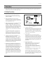
4. Leakage Current Hot Check (Figure 1-1):
Warning: Do not use an isolation
transformer during this test. Use a leakagecurrent tester or a metering system that
complies with American National Standards
Institute (ANIS C101.1, Leakage Current for
Appliances), and Underwriters Laboratories
(UL Publication UL1410, 59.7).
5. With the unit completely reassembled, plug
the AC line cord directly into the power
outlet. With the unit’s AC switch first in the
ON position and then OFF, measure the
current between a known earth ground (metal
water pipe, conduit, etc.) and all exposed
metal parts, including: antennas, handle
brackets, metal cabinets, screwheads and
control shafts. The current measured should
not exceed 0.5 milliamp. Reverse the powerplug prongs in the AC outlet and repeat the
test.
Samsung Electronics
LEAKAGE
CURRENT
TESTER
DEVICE
UNDER
TEST
(READING SHOULD
NOT BE ABOVE
0.5mA)
TEST ALL
EXPOSED METAL
SURFACES
2-WIRE CORD
ALSO TEST WITH
PLUG REVERSED
(USING AC ADAPTER
PLUG AS REQUIRED)
EARTH
GROUND
Fig. 1-1 AC Leakage Test
6. Antenna Cold Check:
With the unit’s AC plug disconnected from the
AC source, connect an electrical jumper across
the two AC prongs. Connect one lead of the
ohmmeter to an AC prong. Connect the other
lead to the coaxial connector.
7. X-ray Limits:
The picture tube is especially designed to
prohibit X-ray emissions. To ensure continued
X-ray protection, replace the picture tube only
with one that is the same type as the original.
Carefully reinstall the picture tube shields and
mounting hardware; these also provide X-ray
protection.
8. High Voltage Limits:
High voltage must be measured each time
servicing is done on the B+, horizontal
deflection or high voltage circuits.
Correct operation of the X-ray protection
circuits must be reconfirmed whenever they
are serviced.
(X-ray protection circuits also may be called
“horizontal disable” or “hold-down”.)
Heed the high voltage limits. These include
the X–ray Protection Specifications Label, and
the Product Safety and X-ray Warning Note on
the service data schematic.
1-1
Precautions
1-1 Safety Precautions (Continued)
9. High voltage is maintained within specified
limits by close-tolerance, safety-related
components and adjustments. If the high
voltage exceeds the specified limits, check
each of the special components.
10. Design Alteration Warning:
Never alter or add to the mechanical or
electrical design of this unit. Example: Do not
add auxiliary audio or video connectors. Such
alterations might create a safety hazard. Also,
any design changes or additions will void the
manufacturer’s warranty.
11. Hot Chassis Warning:
Some TV receiver chassis are electrically
connected directly to one conductor of the AC
power cord. If an isolation transformer is not
used, these units may be safely serviced only
if the AC power plug is inserted so that the
chassis is connected to the ground side of the
AC source.
To confirm that the AC power plug is inserted
correctly, do the following: Using an AC
voltmeter, measure the voltage between the
chassis and a known earth ground. If the
reading is greater than 1.0V, remove the AC
power plug, reverse its polarity and reinsert.
Re-measure the voltage between the chassis
and ground.
12. Some TV chassis are designed to operate with
85 volts AC between chassis and ground,
regardless of the AC plug polarity. These units
can be safely serviced only if an isolation
transformer inserted between the receiver and
the power source.
13. Some TV chassis have a secondary ground
system in addition to the main chassis ground.
This secondary ground system is not
isolated from the AC power line. The two
ground systems are electrically separated by
insulating material that must not be defeated
or altered.
14. Components, parts and wiring that appear to
have overheated or that are otherwise
damaged should be replaced with parts that
meet the original specifications. Always
determine the cause of damage or
overheating, and correct any potential
hazards.
1-2
15. Observe the original lead dress, especially
near the following areas: Antenna wiring,
sharp edges, and especially the AC and high
voltage power supplies. Always inspect for
pinched, out-of-place, or frayed wiring. Do
not change the spacing between components
and the printed circuit board. Check the AC
power cord for damage. Make sure that leads
and components do not touch thermally hot
parts.
16. Picture Tube Implosion Warning:
The picture tube in this receiver employs
“integral implosion” protection. To ensure
continued implosion protection, make sure
that the replacement picture tube is the same
as the original.
17. Do not remove, install or handle the picture
tube without first putting on shatterproof
goggles equipped with side shields. Never
handle the picture tube by its neck. Some
“in-line” picture tubes are equipped with a
permanently attached deflection yoke; do not
try to remove such “permanently attached”
yokes from the picture tube.
18. Product Safety Notice:
Some electrical and mechanical parts have
special safety-related characteristics which
might not be obvious from visual inspection.
These safety features and the protection they
give might be lost if the replacement
component differs from the original—even if
the replacement is rated for higher voltage,
wattage, etc.
Components that are critical for safety are
indicated in the circuit diagram by shading,
(
) or ( ! ).
Use replacement components that have the
same ratings, especially for flame resistance
and dielectric strength specifications.
A replacement part that does not have the
same safety characteristics as the original
might create shock, fire or other hazards.
Samsung Electronics
Precautions
1-2 Servicing Precautions
Warning1: First read the “Safety Precautions” section of this manual. If some unforeseen circumstance creates a conflict between
the servicing and safety precautions, always follow the safety precautions.
Warning2: An electrolytic capacitor installed with the wrong polarity might explode.
1. Servicing precautions are printed on the
cabinet. Follow them.
2. Always unplug the unit’s AC power cord from
the AC power source before attempting to:
(a) Remove or reinstall any component or
assembly, (b) Disconnect an electrical plug or
connector, (c) Connect a test component in
parallel with an electrolytic capacitor.
3. Some components are raised above the printed
circuit board for safety. An insulation tube or
tape is sometimes used. The internal wiring is
sometimes clamped to prevent contact with
thermally hot components. Reinstall all such
elements to their original position.
4. After servicing, always check that the screws,
components and wiring have been correctly
reinstalled. Make sure that the portion around
the serviced part has not been damaged.
Samsung Electronics
5. Check the insulation between the blades of the
AC plug and accessible conductive parts
(examples: metal panels, input terminals and
earphone jacks).
6. Insulation Checking Procedure: Disconnect the
power cord from the AC source and turn the
power switch ON. Connect an insulation
resistance meter (500V) to the blades of the AC
plug.
The insulation resistance between each blade
of the AC plug and accessible conductive parts
(see above) should be greater than 1 megohm.
7. Never defeat any of the B+ voltage interlocks.
Do not apply AC power to the unit (or any of
its assemblies) unless all solid-state heat sinks
are correctly installed.
8. Always connect a test instrument’s ground
lead to the instrument chassis ground before
connecting the positive lead; always remove
the instrument’s ground lead last.
1-3
Precautions
1-3 Precautions for Electrostatically Sensitive Devices (ESDs)
1. Some semiconductor (“solid state”) devices
are easily damaged by static electricity. Such
components are called Electrostatically
Sensitive Devices (ESDs); examples include
integrated circuits and some field-effect
transistors. The following techniques will
reduce the occurrence of component damage
caused by static electricity.
2. Immediately before handling any semicon
ductor components or assemblies, drain the
electrostatic charge from your body by
touching a known earth ground. Alternatively,
wear a discharging wrist-strap device. (Be
sure to remove it prior to applying power—
this is an electric shock precaution.)
3. After removing an ESD-equipped assembly,
place it on a conductive surface such as
aluminum foil to prevent accumulation of
electrostatic charge.
4. Do not use freon-propelled chemicals. These
can generate electrical charges that damage
ESDs.
1-4
5. Use only a grounded-tip soldering iron when
soldering or unsoldering ESDs.
6. Use only an anti-static solder removal device.
Many solder removal devices are not rated as
“anti-static”; these can accumulate sufficient
electrical charge to damage ESDs.
7. Do not remove a replacement ESD from its
protective package until you are ready to
install it. Most replacement ESDs are
packaged with leads that are electrically
shorted together by conductive foam,
aluminum foil or other conductive materials.
8. Immediately before removing the protective
material from the leads of a replacement ESD,
touch the protective material to the chassis or
circuit assembly into which the device will be
installed.
9. Minimize body motions when handling
unpackaged replacement ESDs. Motions such
as brushing clothes together, or lifting a foot
from a carpeted floor can generate enough
static electricity to damage an ESD.
Samsung Electronics
Reference Information
2. Reference Information
2-1 Tables of Abbreviations and Acronyms
Table 2-1 Abbreviations
A
Ah
Å
dB
dBm
°C
°F
°K
F
G
GHz
g
H
Hz
h
ips
kWh
kg
kHz
kΩ
km
km/h
kV
kVA
kW
I
MHz
Samsung Electronics
Ampere
Ampere-hour
Angstrom
Decibel
Decibel Referenced to One
Milliwatt
Degree Celsius
Degree Fahrenheit
degree Kelvin
Farad
Gauss
Gigahertz
Gram
Henry
Hertz
Hour
Inches Per Second
Kilowatt-hour
Kilogram
Kilohertz
Kilohm
Kilometer
Kilometer Per Hour
Kilovolt
Kilovolt-ampere
Kilowatt
Liter
Megahertz
MV
MW
MΩ
m
µA
µF
µH
µm
µs
µW
mA
mg
mH
mI
mm
ms
mV
nF
Ω
pF
Ib
rpm
rps
s
V
VA
W
Wh
Megavolt
Megawatt
Megohm
Meter
Microampere
Microfarad
Microhenry
Micrometer
Microsecond
Microwatt
Milliampere
Milligram
Millihenry
Milliliter
Millimeter
Millisecond
Millivolt
Nanofarad
Ohm
Picofarad
Pound
Revolutions Per Minute
Revolutions Per Second
Second (Time)
Volt
Volt-ampere
Watt
Watt-hour
2-1
Reference Information
Table 2-2 Table of Acronyms
ABL
AC
ACC
AF
AFC
AFT
AGC
AM
ANSI
APC
APC
A/V
AVC
BAL
BPF
B-Y
CATV
CB
CCD
CCTV
Ch
CRT
CW
DC
DVM
EIA
ESD
ESD
FBP
FBT
FF
FM
FS
GND
G-Y
H
HF
HI-FI
IC
IC
IF
2-2
Automatic Brightness Limiter
Alternating Current
Automatic Chroma Control
Audio Frequency
Automatic Frequency Control
Automatic Fine Tuning
Automatic Gain Control
Amplitude Modulation
American National Standards Institute
Automatic Phase Control
Automatic Picture Control
Audio-Video
Automatic Volume Control
Balance
Bandpass Filter
Blue-Y
Community Antenna Television (Cable TV)
Citizens Band
Charge Coupled Device
Closed Circuit Television
Channel
Cathode Ray Tube
Continuous Wave
Direct Current
Digital Volt Meter
Electronics Industries Association
Electrostatic Discharge
Electrostatically Sensitive Device
Feedback Pulse
Flyback Transformer
Flip-Flop
Frequency Modulation
Fail Safe
Ground
Green-Y
High
High-Frequency
High Fidelity
Inductance-Capacitance
Integrated Circuit
Intermediate Frequency
I/O
L
L
LED
LF
MOSFET
MTS
NAB
NEC
NTSC
OSD
PCB
PLL
PWM
QIF
R
RC
RF
R-Y
SAP
SAW
SIF
SMPS
S/N
SW
TP
TTL
TV
UHF
UL
UV
VCD
VCO
VCXO
VHF
VIF
VR
VTR
VTVM
TR
Input/output
Left
Low
Light Emitting Diode
Low Frequency
Metal-Oxide-Semiconductor-Field-Effect-Tr
Multi-channel Television Sound
National Association of Broadcasters
National Electric Code
National Television Systems Committee
On Screen Display
Printed Circuit Board
Phase-Locked Loop
Pulse Width Modulation
Quadrature Intermediate Frequency
Right
Resistor & Capacitor
Radio Frequency
Red-Y
Second Audio Program
Surface Acoustic Wave(Filter)
Sound Intermediate Frequency
Switching Mode Power Supply
Signal/Noise
Switch
Test Point
Transistor Transistor Logic
Television
Ultra High Frequency
Underwriters Laboratories
Ultraviolet
Variable-Capacitance Diode
Voltage Controlled Oscillator
Voltage Controlled Crystal Oscillator
Very High Frequency
Video Intermediate Frequency
Variable Resistor
Video Tape Recorder
Vacuum Tube Voltmeter
Transistor
Samsung Electronics
Reference Information
2-2 IC Line Up
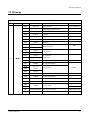
Table 2 - 3 IC Line - Up
NO
1
BOARD
MAIN
LOC. NO
SPEC
IC201S
VDP3112B
Video Processor
Refer to Table 2-3-1
IC601
MSP3410D
Multistandard Sound Processor
Refer to Table 2-3-2
IC901
SDA555X
MICOM, TTX(MTP)
IC902
KS24L161
EEPROM
IC602
TDA7297
Audio AMP
HIC201
DRGB001
RGB Drive AMP Hybrid IC
IC301
LA7845
Q401
KSD5703
D409
FMP-3FU
IC401
KA393
Q404
IRF620
IC801S
3S1265RD
3S1265R
D801S
RBV606
Bridge Diode
PC801S
PC123Y
Photo Coupler
IC805
KA78R05
5V Controlled Regulator
D806
Rectifier Diode
D807
FML-G12S
F10V20S
D805
FMG-G26S
F10V60S
IC804
KA7806
6V Regulator
IC803
KA78R08
8V Controlled Regulator
IC903
KA78RM33
3.3V Regulator
IC904
KIA7025AP
MICOM Reset IC
2N7000
IIC Level Shifter
Q909
DESCRIPTION
REMARK
Refer to Table 2-3-3
VM Option
Vertical IC
Horizontal Drive IC
DH01
E/W Drive IC
SPS Controllor
DDR01
Q910
Samsung Electronics
TU01
TCPS3001PD09D(S)
D813
FML-G12S
Main Tuner with IF Block
Refer to Table 2-3-4
Rectifier Diode
2-3
Reference Information
Table 2 - 3 IC Line - Up
NO
BOARD
LOC. NO
SPEC
DESCRIPTION
REMARK
IC501
TDA6101Q
Video Output AMP R.G.B Drive
PCB Version
A,B,C,D
IC501
STV5109
Video Output AMP R.G.B Drive
PCB Version
F,G,H,J
Video Switching IC with Adder Output
Option
High-end Picture-In Picture IC
Option
IC502
CRT
2
2-4
IC503
3
V-S/W
ICS01
TEA6425
4
PIP
ICP01
SDA9488X
Samsung Electronics
Reference Information
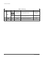
Table 2-3-1 VIDEO IC
FUNCTION
SPEC
VDP3112B
VDP3130Y-B2
REMARK
50Hz Basic 1H Comb Filter
50Hz, 2H Comb Filter, DVD Input
Table 2-3-2 SOUND IC
FUNCTION
SPEC
MSP3400D
Multistandard, A2 Stereo, Equalizer, 2 Scart, RCA9P
MSP3410D
Multistandard, A2 Stereo, Nicam, Equalizer, 2 Scart, RCA9P
MSP3405D/BSP3505D
REMARK
Multistandard, Line-Stereo, Mono, RCA9P
Table 2-3-3 SOUND AMP
SPEC
TDA7297
15W x 2CH, 10W x 2CH
TDA7266S
5W x 2CH
FUNCTION
REMARK
FUNCTION
REMARK
Table 2-3-4 TUNER
SPEC
TCPS3001PD09A(S)
CS, Stereo
IF IC = Sanyo
TCPS3001PD09D(S)
CS, Stereo
IF IC = Philips
TCPS3001PD09C(S)
CS, Stereo, India
TAFC-Z141D
CS, Stereo
Table 2-3-5 HORIZONTAL DRIVE IC (Q401)
FUNCTION
SPEC
KSD5703
50Hz, With EW Model
KSC5386
50Hz, W/O EW Model
Samsung Electronics
REMARK
2-5
MEMO
2-6
Samsung Electronics
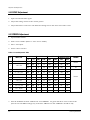
Specifications
3. Specifications
Television
System
CS
PAL/SECAM-B/G,D/K,I, NTSC-M
CZ
PAL/SECAM-B/G,D/K,I, NTSC4.43
Antena Input
Consumption
Power
Requirements
75ohms, Coaxial Cable
65W (Applied When 21” Flat)
220V Only
Free Voltage
Frequency
Depending on Tuner
Not Present R815
50/60Hz
15W x 2CH
Output
10W x 2CH
5W x 2CH
Sound
Effect
Turbo Sound
Pseudo Stereo
RCA Input
Front
(AV2)
S-VHS
Option
Head-Phone
Jacks
Back
2Scart Input/Output
AV1 : Scart I/O, RGB Input,
RF Out
AV2 : Scart I/O, Monitor Out
DVD Input(YPbPr)
Option
RCA Input/Output
AV1: Video/Audio-R/Audio-L
AV2: Video/Audio-R/Audio-L
Monitor Out : Video/AudioR/Audio-L
S-VHS
Option
Specifications are subject to change.
Samsung Electronics
3-1
MEMO
3-2
Samsung Electronics
Alignment and Adjustments
4. Alignment and Adjustments
4-1 General Alignment Instructions
1. Usually, a color TV-VCR needs only slight
touch-up adjustment upon installation. Check
the basic characteristics such as height,
horizontal and vertical sync and focus.
5. Avoid overload. Excessive signal from a
sweep generator might overload the front-end
of the TV. When inserting signal markers, do
not allow the marker generator to distort test
results.
2. Observe the picture for good black and white
details. There should be objectionable color
shading; if color shading is present,
demagnetize, perform purity and convergence
adjustments described below.
6. Connect the TV only to an AC power source
with voltage and frequency as specified on the
backcover nameplate.
3. Use the specified test equipment or its
equivalent.
7. Do not attempt to connect or disconnect any
wires while the TV is turned on. Make sure
that the power cord is disconnected before
replacing any parts.
4. Correct impedance matching is essential.
8. To protect against shock hazard, use an
isolation transformer.
4-2 Automatic Degaussing
A degaussing coil is mounted around the
picture tube, so that external degaussing after
moving the TV should be unnecessary. But
the receiver must be properly degaussed upon
installation.
The degaussing coil operates for about 1
second after the power is switched ON. If the
set is moved or turned in a different direction,
the power should be OFF for at least 10
minutes.
If the chassis or parts of the cabinet become
magnetized, poor color purity will result. If
this happens, use an external degaussing coil.
Slowly move the degaussing coil around the
faceplate of the picture tube and the sides and
front of the receiver. Slowly withdraw the coil
to a distance of about 6 feet before turning
power OFF.
If color shading persists, perform the
following Color purity and Convergence
adjustments.
4-3 High Voltage Check
CAUTION : There is no high voltage adjustment
on this chassis. The B+ power supply should be
+135 volts (with full color- bar input and normal
picture level).
1. Connect a digital voltmeter to the second
anode of the picture tube.
2. Turn on the TV. Set the Brightness and
Contrast controls to minimum (zero beam
current).
3. Adjust the Brightness and contrast controls to
both extremes. Ensure that the high voltage
does not exceed 30 KV under any conditions.
Samsung Electronics
4-1
Alignment and Adjustments
4-4 FOCUS Adjustment
1. Input a black and white signal.
2. Adjust the tuning control for the clearest picture.
3. Adjust the FOCUS control for well defined scanning lines in the center area of the screen.
4-5 SCREEN Adjustment
1. Input Toshiba Pattern
2. Enter “Service Mode”.(Refer to “4-8-1 Service Mode”)
3. Select “G2-Adjust”.
4. Set the values as below.
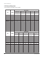
Table 1. Screen Adjustment Table
IBRM
No
1
2
14” / SDI
15PF / SDI
CDL
WDRV
INCH / CRT
COLR G B
(Smallesz Value)
5109
6101
6101
5109
6101
5109
6101
5109
205
205
35
35
100
100
100
100
220
225
35
35
200
160
65
100
215
215
35
35
100
100
100
100
3
21” 1.7R / SDI
220
215
35
45
230
160
65
80
4
21” 1.7R / JCT
220
220
35
35
200
200
150
150
5
21PF / TSB
220
225
35
45
230
185
65
75
6
21PF / LG
230
225
35
45
230
175
65
165
7
21PF / SDI
220
220
35
35
230
200
65
145
8
25PF / SDI
210
205
35
45
150
150
65
140
9
29” 1.3R / SDI
220
200
35
45
180
180
65
150
10
25” 1.3R/SDI
220
210
35
35
230
220
65
130
11
30”
210
200
35
45
160
180
100
130
REGION
Noraml
CIS
Noraml
5. Turn the SCREEN VR until “MRCR G B” and “MRWDG” are green and those value are about 100.
(The incorrect SCREEN Voltage may result that “MRCR G B” and “MRWDG” should be red)
4-2
Samsung Electronics
Alignment and Adjustments
4-6 E2PROM (IC902) Replacement
1. When IC902 is replaced, all adjustment data revert to the initial values.
So, all adjustment values when servicing should be readjusted.
2. After IC902 is replaced, connect the AC power supply cord.
3. Turn the power switch ON.
4. In stand-by, warm up the TV for at least 10 seconds.
5. Power on the TV.
4-7 White Balance Adjustment
■ Equipment : Color-Analyzer (CA-100)
■ Input Signal : Pattern signal (Toshiba pattern)
1. Select STANDARD from the menu.
2. Input an 100% White pattern.
3. Enter the “Service Mode”. (Refer to “4-8 Service Mode”)
4. Warm up the TV set at least for 30 minutes.
5. Input a Toshiba pattern signal.
6. Enter the “Video Adjust1”. (Refer to table 2.)
- Adjust “Sub Contrast” so that Y (luminance) becomes 65 ft ± 3.
- Use “Red Drive” and “ Blue Drive” to adjust High-Light (x : 265, y : 265)
- Adjust “Sub Bright” so that Y (luminance) becomes 1.2ft ± 0.3.
- Use “Red Cutoff” and “Blue Cutoff” to adjust Low-Light (x : 265, y : 265).
7. Adjust CA-100 so that the final adjustment value can be fixed.
8. Use the Channel Up/Down (▲/▼) buttons to move the cursor on the adjustment modes.
9. Use the Volume +/- buttons to change the adjustment value.
Samsung Electronics
4-3
Alignment and Adjustments
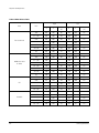
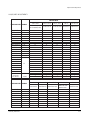
Table 2. White Balance Table
High
Area
East South Asia
Middle East Asia
& Africa
CIS
Australia
4-4
Inch
Low
X
Y
Luminance
(ft)
X
Y
Luminance
(ft)
15PF
265
265
85
265
265
1.8
21” 1.7R
265
265
50
265
265
1.2
21PF
265
265
60
265
265
1.0
25”1.3R
265
265
45
265
265
1.0
25PF
265
265
40
265
265
1.2
29”1.3R
265
265
35
265
265
1.0
30”
265
265
35
265
265
1.0
14”
290
300
55
290
300
1.8
15PF
290
300
85
290
300
1.8
21” 1.7R
290
300
50
290
300
1.2
21PF
290
300
60
290
300
1.0
25” 1.3R
290
300
45
290
300
1.0
25PF
290
300
40
290
300
1.2
29”1.3R
290
300
35
290
300
1.0
30”
290
300
35
290
300
1.0
15PF
272
270
50
265
266
2.2
21PF
272
270
50
265
266
2.0
25” 1.3R
272
270
40
265
266
2.2
25PF
272
270
30
265
266
2.2
29” 1.3R
272
270
30
265
266
2.2
15PF
292
307
85
301
311
1.8
21PF
292
307
60
301
311
1.0
25” 1.3R
292
307
45
301
311
1.0
25PF
292
307
40
301
311
1.2
29” 1.3R
292
307
35
301
311
1.0
Samsung Electronics
Alignment and Adjustments
4-8 Factory Adjustment
4-8-1 Service Mode
1. To enter the “Service Mode”, Press the remote-control keys in this sequence :
- If you do not have Factory remote-control
PICTURE OFF
DISPLAY (
)
MUTE
MENU
PICTURE ON
- If you have Factory remote-control
PICTURE ON
DISPLAY (
)
FACTORY
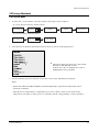
2. After the Service Mode is entered, the initial screen is as shown in the figure below.
xx xx xx *
These hexa digits are check sum value which
* depends
on the MICOM version.
If check sum value is changed, the value of
2
E PROM Data newly initialed.
3. Use the Channel Up/Down buttons to move the cursor in the adjustment parameters.
Note :
2
- When CRT, CRT PCB, FBT, E PROM (sometimes MICOM) is replaced, the adjustment values
should be controlled.
- After the Service adjustment is completed, Do not select “Reset” in the service mode menu.
(After above procedure is done, power is on initially and the “Plug and Play” will be operated.)
Samsung Electronics
4-5
Alignment and Adjustments
Area
Micom Version
SIM-806EW
(KS2A/KS3A)
EUROPE
Excluded Model
Main Problems & History of Corrections
MSP3410 94 58 VERSION At the current mass production (MP), MASK is applying
to ks2a/ks3a chassis
SIM-806EW1
(KS2A/KS3A)
1. Improvement of Secam-L Sound Noise when using MSP3410
94 58 VERSION
2. Improvement of repetition of SECAM-L in AUTO SEARCH
3. Improvement of the gap between SCART RGB and CVBS image
centers .(Added to RGB SHIFT FACTORY)
4. Correction of Greek OSD
5. Fixation of Zoom Mode Offset Changed in order to adjust in Service
mode. Application of REMASK via an improvement in picture quality
SIM-806EW2
Application of REMASK via an improvement in picture quality
OIM-806EW
(KS2A/KS3A)
TOSHIBA OEM MODEL ONLY MICOM (Applied to SEH MP)
SIM-806MA CONTROL 6KEY,PIP MODEL, MTP is used for all models (excluding KS2A 22Q)
(KS2A)
All 22-Q models
MTP used for KS2A 22Q models
1. VM related items (Delay1,Gain1,Limit,Delay,Coring) Adjust3)
2. Addition of PIP VSPDEL to FACTORY items
3. No color when PIP NTSC 4.43 is received
4. NICAM POP NOISE
5.Av by channel key added
6.When English is used for the language of Libia models, the Libian
must be added and PROGRAM_OSD box must be reduces (Libian Only)
Middle SIM-806MA1
(KS2A/KS3A)
East
Asia
& Africa
& CIS
7. RGB SHIFT/HB START/HB STOP added
8. Countermeasure on RADIATION (Option: Pin49 output software)
9. In NTSC system, a transient phenomenon happens during the channel
SIM-806MA2
(KS2A/KS3A)
Decided to apply MASK
(June 2001)
1. Improvement of SECAM/PAL Color Hysteresis characteristics
2. Correction of instantaneous LNA error
SIM-806MA3
(KS2A/KS3A)
SIM-806EA
(KS2A)
SIM-806EAY
(KS2A)
East
South
Asia
&
Australia
4-6
SIM-806EA1
(KS2A/KS3A)
Correction of Libian about child lock
Thailand,Vietnam,
PIP MODEL,6-KEY,CONTROL
MTP used for KS2A
1. Correction of Thailand/Vietnam OSD problems
("Not available", "S-Video")
1. Change of Indonesia sports string
2. Addtion of VM related items (Delay1,Gain1,Limit,Delay,Coring)
to Adjust3
3. Addition of PIP VSPDEL to FACTORY items
4. Improvement of No Color when PIP NTSC 4.43 is received
5. Improvement of NICAM POP NOISE
6. Addition of AV by channel key service
7. Addition of RGB SHIFT/HB START/HB STOP
8. Addition of countermeasure on RADIATION (Option: pin49 output
software)
9. Transient phenomena when switching CH in NTSC system
10. In Temperature Low test, the color of SECAM CH' late follows
Samsung Electronics
Alignment and Adjustments
Area
Micom Version
Excluded Model
Main Problems & History of Corrections
East
South SIM-806EA1 Checking the improvement
Asia
(KS2A/KS3A) in quality: Vietnam/Thailand
&
28.Dec.2000
Australia
SIM-806C
(KS2A/KS3A)
Same with MTP (developed in 22 Sep. 2000)
1. Improvement of color noise in LOW BURST
China
SIM-806C1
(KS2A/KS3A)
2. A sound saw filter switching error happens when changing Manual
Color System
(For a PAL channel, when switching NTSC3.58 into Auto)
3. Addition of PIP VSPDEL to FACTORY items
4. Improvement of No Color when PIP NTSC 4.43 is received
5. Addition of RGB SHIFT/HB START/HB STOP
6. Addition of countermeasure on RADIATION (Option: pin 49 output
software)
7. Transient phenomena happens when switching CH' in NTSC system
SIM-806EI
(KS2A/KS3A)
India
SIM-806EI1
(KS2A/KS3A)
Samsung Electronics
Same with MTP (developed in 6 Sep. 2000)
1. Addition of PIP VSPDEL to FACTORY items
2. Improvement of No Color when PIP NTSC 4.43 is received
3. Addtion of RGB SHIFT/HB START/HB STOP
4. Addition of countermeasure on RADIATION (Option: pin49 output
software)
5. Transient phenomena happens when switching CH' in NTSC system
6. In Temperature Low test, the color of SECAM CH' late follows.
7. Addition of woofer to FACTORY items
8. Change of the value of equalizer (Factory Woofer in EQ ON)
4-7
Alignment and Adjustments
4-8-2 Deflection (Memory Data)
4-8-2(A) GEOMETRIC ADJUSTMENT VALUE BY MODEL
INITIAL DATA
OSD
RANGE
TSB 21-FLAT
LG-CPT 21-FLAT
SDI 21" FALT
SDI 14"
SDI 15" FLA
A51LSH196X03(+380)
A51QDJ279X14 A51QDX991X001 A34KQV42X A36QDT351X
A51LSH198X03(-250)
V SHIFT
V AMP
V SLOPE
V SC
H EW
H TRAPEZIUM
H PARABOLA
H SYMMETRY
H CORNER
H SHIFT
PIP CONTRAST
PIP TINT
PIP VSPDEL
PIP PAL V. POS
PIP NTSC V. POS
PIP H. POS
PIP BLKLG
-128~127
-128~127
-128~127
-128~127
-128~127
-128~127
-128~127
-128~127
-128~127
-128~127
0~15
0~63
0~32
0~255
0~255
0~255
0~15
-40
20
0
-13
50
20
15
13
40
0
7
0
0
33
33
45
6
-40
20
-5
-6
-30
20
15
13
40
0
15
0
8
33
33
45
6
-40
-15
0
-13
20
-40
20
13
40
0
7
0
8
33
33
45
6
-20
-40
-5
0
61
-8
-3
12
-32
0
7
0
0
33
33
45
6
-18
18
-4
-17
24
20
17
5
69
0
7
0
0
33
33
45
6
SDI 29" 1.3R
SDI 30"
INITIAL DATA
OSD
RANGE
SDI 21"1.7R
SDI 25" 1.3R
SDI 25" FLAT
A51KQJ63X01 A59KPR84X01 A59QDF891X002
V SHIFT
V AMP
V SLOPE
V SC
H EW
H TRAPEZIUM
H PARABOLA
H SYMMETRY
H CORNER
H SHIFT
PIP CONTRAST
PIP TINT
PIP VSPDEL
PIP PAL V. POS
PIP NTSC V. POS
PIP H. POS
PIP BLKLG
4-8
-128~127
-128~127
-128~127
-128~127
-128~127
-128~127
-128~127
-128~127
-128~127
-128~127
0~15
0~63
0~32
0~255
0~255
0~255
0~15
-40
5
-2
-7
64
-20
-13
13
15
0
7
0
0
33
33
45
6
-50
-10
0
-6
10
-50
-40
13
40
0
7
0
0
33
33
45
6
-50
-15
0
-13
10
-10
-60
13
69
0
7
0
8
33
33
45
6
A68QBT891X002
A70QBZ791X001
A68KVL74X01
-50
-20
0
0
-55
-40
-60
13
70
0
7
0
0
33
33
45
6
-40
-48
-2
0
20
-80
-75
13
60
-2
7
0
14
33
33
45
6
Samsung Electronics
Alignment and Adjustments
4-8-2(B) GEOMETRIC ADJUSTMENT
OSD
RANGE
V SHIFT
-128~127
V AMP
-128~127
V SLOPE
V SC
-128~127
-128~127
H EW
-128~127
H TRAPEZIUM
H PARABOLA
H SYMMETRY
-128~127
-128~127
-128~127
H CORNER
-128~127
H SHIFT
PIP CONTRAST
PIP TINT
-128~127
0~15
0~63
PIP VSPDEL
0~32
PIP PAL V. POS
PIP NTSC V. POS
PIP H. POS
PIP BLKLG
0~255
0~255
0~255
0~15
Samsung Electronics
FUNCTION
Adjusts Vertical picture position
Adjusts Vertical picture size. Adjust 4:4 upper and below picture size in lion head
pattern at factory
Adjusts Vertical Slope Correction
Adjusts Vertical s-correction
Horizontal east west width. Adjust 5:5 left and right picture size in lion head pattern
at factory.
Adjusts horizontal Trapezium.
Adjusts Horizontal Parabola.
Adjusts the top and bottom horizontal symmetry of picture.
Adjusts the top and bottom horizontal corner of picture.
Adjusts so that the top and bottom of H corner can be linear.
Adjusts Horizontal Position.
Adjusts PIP contrast.
Adjusts PIP Tint. When a NTSC signal is received, this PIP Tint adjusts color phase
PIP vertical sync pulse delay. When chaning data, PIP jitters at two points. In this case,
the PIP VSPDEL is set to the center between two points.
Adjust Vertical position the PIP of PAL system.
Adjust Vertical position the PIP of NTSC system.
Adjust Horizontal Position the PIP.
Adjusts PIP blanking level green (PIP low light white balance).
4-9
Alignment and Adjustments
4-8-2(C) SCREEN CHANGE (I2C BUS GEOMETRIC ADJUSTMENT)
1
V Shift
6
V Amp
2
V Slope
7
V SC
3
H EW
8
H Trapizium
4
H Parabola
9
H Symmetry
5
H Corner
10
H Shift
4-10
Samsung Electronics
Alignment and Adjustments
4-8-2(D) VIDEO ADJUSTMENT 1
INITIAL DATA
VIDEO ADJUST1 RANGE
TSB 21-FLAT
LG-CPT 21-FLAT
SDI 21" FALT
SDI 14"
SDI 15" FLA
A51LSH196X03(+380)
A51QDJ279X14 A51QDX991X001 A34KQV42X A36QDT351X
A51LSH198X03(-250)
RED CUTOFF
GREEN CUTOFF
BLUE CUTOFF
RED DRIVE
GREEN DRIVE
BLUE DRIVE
SUB BRIGHT
SUB CONTRAST
SUB COLOR
SUB TINT
BCL THRESHOLD
BCL GAIN
BCL TIME
TTX CONTRAST
P. BG YC DELAY
P. DK YC DELAY
P.I YC DELAY
P.M YC DELAY
S. BG YC DELAY
S. DK YC DELAY
S.I YC DELAY
N.M YC DELAY
P. YC DELAY
S. YC DELAY
N. YC DELAY
0~255
0~255
0~255
0~255
0~255
0~255
0~200
0~63
0~27
0~100
0~255
0~15
0~15
0~255
RF
VIDEO
MODE
127
127
127
127
127
127
100
52
27
30
62
9
5
90
3
6
6
3
3
5
5
7
4
1
4
127
127
127
127
127
127
100
52
27
30
54
8
13
90
3
6
6
3
3
5
7
3
4
1
4
127
127
127
127
127
127
100
52
27
30
62
8
13
90
3
6
6
3
3
5
7
3
4
1
4
127
127
127
127
127
127
100
52
27
30
30
8
13
90
3
6
6
3
3
5
7
3
4
1
4
127
127
127
127
127
127
100
52
27
30
35
8
13
100
3
6
6
3
3
5
7
3
4
1
4
INITIAL DATA
VIDEO ADJUST1 RANGE
SDI 21"1.7R
SDI 25" 1.3R
SDI 25" FLAT
A51KQJ63X01 A59KPR84X01 A59QDF891X002
RED CUTOFF
GREEN CUTOFF
BLUE CUTOFF
RED DRIVE
GREEN DRIVE
BLUE DRIVE
SUB BRIGHT
SUB CONTRAST
SUB COLOR
Samsung Electronics
0~255
0~255
0~255
0~255
0~255
0~255
0~200
0~63
0~27
127
127
127
127
127
127
100
52
27
127
127
127
127
127
127
100
52
27
127
127
127
127
127
127
110
52
27
SDI 29" 1.3R
SDI 30"
A68QBT891X002
A70QBZ791X001
A68KVL74X01
127
127
127
127
127
127
100
52
27
127
127(FIX)
127
127
127(FIX)
127
100
52
27
4-11
Alignment and Adjustments
INITIAL DATA
VIDEO ADJUST1
RANGE
SDI 21"1.7R
SDI 25" 1.3R
SDI 25" FLAT
A51KQJ63X01 A59KPR84X01 A59QDF891X002
SUB TINT
BCL THRESHOLD
BCL GAIN
BCL TIME
TTX CONTRAST
P. BG YC DELAY
P. DK YC DELAY
P.I YC DELAY
P.M YC DELAY
S. BG YC DELAY
S. DK YC DELAY
S.I YC DELAY
N.M YC DELAY
P. YC DELAY
S. YC DELAY
N. YC DELAY
0~100
0~255
0~15
0~15
0~255
RF
VIDEO
MODE
VIDEO ADJUST 1
RANGE
RED CUTOFF
GREEN CUTOFF
BLUE CUTOFF
RED DRIVE
0~255
0~255
0~255
0~255
GREEN DRIVE
0~255
BLUE DRIVE
SUB BRIGHT
0~255
0~200
SUB CONTRAST
0~63
SUB COLOR
SUB TINT
BCL THRESHOLD
BCL GAIN
BCL TIME
TTX CONTRAST
0~27
0~100
0~255
0~15
0~15
0~255
YC DELAY
4-12
0~8
30
40
8
13
90
3
6
6
3
3
5
7
3
4
1
4
30
60
9
7
70
3
6
6
3
3
5
7
3
4
1
4
30
67
9
13
90
3
6
6
3
3
5
7
3
4
1
4
SDI 29" 1.3R
SDI 30"
A68QBT891X002
A70QBZ791X001
A68KVL74X01
30
67
8
13
90
3
6
6
3
3
5
7
3
4
1
4
30
64
9
7
70
3
6
6
3
3
5
7
3
4
1
4
FUNCTION
Adjusts the gain red output of low light.
Adjusts the gain green output of low light. Fix this agin to 127.
Adjusts the gain blue output of low light.
Adjusts the red blue output of high light.
Adjusts the green output of high light. After "G2-Adjustment" and White Balance
adjustments are complete, this data is fixed
Adjusts the gain blue output of high light.
Adjust sub brightness level to set the low luminance in Picture Standard mode.
Adjusts sub contrast level to set the high luminance in Pitture Standard mode.
Set the value of sub contrast to near 50. The user control " contrast" depends on this value.
User contrast=[sub cont x 2/100] If sub contrast data is 10, user contrast changes into
1/5 step
Adjusts sub color level to set the gain for color in Picture Standard mode.
Adjusts the sub tint level of NTSC color system.
Short for Beam Current Limit Threshold. Adjusts the current of CRT long term.
Beam current limit gain
Adjusts BCL Time constant. Beam current limit actual time
Adjusts contrast on TTX picture.
Compensates the time gap between color and luminance boundaries and cotrolls data
difference by system(See table above)
Samsung Electronics
Alignment and Adjustments
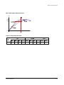
Note 1. Beam Control Limit Characteristic
beam
MIN
1.8mA
1.6mA
BCL GAIN
BCL THESHOLD
MAX
WDRGB
50
IRE
Table 3. YC Delay Adjustment Table
PAL
NTSC
SECAM
YC
Delay
Def.
BG
DK
I
Def.
BG
DK
I
Def.
M
Value
4
3
6
6
1
3
5
7
4
0
Samsung Electronics
4-13
Alignment and Adjustments
4-8-2(E) VIDEO 2 ADJUST
INITIAL
RANGE VALUE
OSD
B STRETCH-BTHR
B STRETCH-BTLT
B STRETCH-BAM
CORING
RGB BRIGHT
RGB CONTRAST
0 ~ 55
0 ~ 15
0 ~ 31
0 ~ 31
0 ~ 255
0 ~ 80
EHT TIME
0 ~ 15
EHT VERTICAL
0 ~ 255
50
8
4
31
45
0
3112B:0
3130Y:3
60
FUNCTION
Black stretch threshold
Black stretch tilt position
Black stretch amount
Luminance peaking filter coring
External RGB brightness
External RGB contrast
Electronics high tension time
EHT vertical correction time(according to beam change)
EHT compensation coefficent vertical
REMARKS
DIGITAL NR OFF VALUE
SCARTS MODEL ONLY
SCARTS MODEL ONLY
VDP3130Y NO USED '0'
Lmax
Lout
Ltr
Lt
BAM
BTLT
Lmin
4-14
Samsung Electronics
Alignment and Adjustments
4-8-2(F) VIDEO 3 ADJUST
ADD ITEM
OSD
RANGE
INITIAL
VALUE
PEAK THRESHOLD
SOFT LIMIT SLOPE B
HARD LIMIT
PEAK VIDEO REF
PEAK VIDEO GAIN
ACC-REF(PAL/NTSC)
ACCR(SECAM)
Gain1(video
Delay1(video)
Velocity Limt
Velocity Delay
Velocity Coring
0~255
0~15
0~255
0~4
0~5
0~40
0~39
0~31
0~15
0~127
0~15
0~15
255
4
255
0
0
33
21
11
3
74
7
10
RGB SHIFT
0~255
109
HB START
0~255
117
HB STOP
0~255
168
2H Comb Filter
0~1
NR OFF Value
Color Hys(SECAM)
Color Hys(PAL)
0~10
0~255
0~255
Samsung Electronics
1
0
166
200
FUNCTION
REMARKS
White peak level threshold
Design factor
Refer to picture below
Design factor
White peak levelthrehold reference
White peak level threshild gain
Auto color control gain(PAL/NTSC)
Auto color control gain(SECAM)
Velocity video gain
Velocity video delay
Velocity limit
Velocity delay
Velocity frequency coring
Design factor
Design factor
Picture standard color gain setting
Picture standard color gain setting
Not used(design factor)
Not used(design factor)
Not used(design factor)
Not used(design factor)
Not used(design factor)
Used to scarts model only.
Adjust RGB input signal Horizontal position
VDP3130Y:Not used
Picture right edge position SAG
Horizontal blainking start
or cut problem countermeasure
Picture left edge position SAG
Horizontal blainking stop
or cut problem countermeasure
OFF(0):Cross color and Dot crawl
Comb filter on/off ( 0 : Comb fillter off
phenomenons happen. Detailed
1 : Comb filtter on )
characteristics are a little good.
VDP3108:No comb filter, VDP3112B/
ON(1): Cross color and Dot crawl
VDP3130Y/VDP3120B:Comb Filter
characteristics are good, but Detaile
function present
characteristics aren't
Adjust Digital NR off value
Picture standard mode detail
Color killing hysteresys(SECAM)
0 ~ 155 Not used(SECAM NO COLOR)
Color killing hysteresys(PAL)
4-15
Alignment and Adjustments
4-8-2(G) OPTION 1
Micom Spec : SIM-806EA
ITEM(OSD)
No.
1
Language
2
Sound
3
CRT
4
AV Mode
5
x-ray
6
Tilt Control
7
Auto FM
8
PIP
Control
ESAsia
A2/NICAM
Virtual Dolby
Mono
Line-Stereo
4:3
Wide
Q(12.8:9)
4:3-16:9
Q - 16:9
1Scart
2Scart
2scart+S
1RCA
2RCA
2RCA+S
2RCA+D
2RCA+S+D
On
Off
On
Off
On
Off
Off
1 - tuner
2 - tuner
West Europe
East Europe
9
Txt Language
10
LNA
11
Equalizer
12
High deviate
13
TTX On/OFF
14
AV by CH Key
4-16
Russian
Greek-Turkey
Arabic
Farsi
Arab-Hebrew
On
Off
On
Off
On
Off
On
Off
On
Off
Description
ENGLISH/VIETNAM/THAI/INDONESIA/MALAYSIA
A2 Stereo / Nicam Stereo Model
Virtual Dolby Model
Mono Model
Line stereo Model
Normal / Zoom / 16:9
Wide CRT ( 16:9 )
Plus / Normal / Zoom / 16:9
Normal / Zoom
Plus / Normal / Zoom
Built in 1 Scart Model
Built in 2 Scart Model
Built in 2 Scart +SVHS JACK Model
Built in RCA 6P / RCA 4P Model
Built in RCA 9P Model
Built in RCA 9P + SVHS JACK Model
Built in RCA 9P + DVD JACK Model
Built in RCA 9P + SVHS JACK Model +DVD JACK Model
X-ray detection function on
X-ray detection function off
CRT Tilt control function on ( wide / 29PF CRT)
CRT Tilt control function off
automatic change from NICAM to FM depends on NICAM error rate
automatic change from NICAM to FM depends on NICAM syncronization
no PIP function
1 Tuner PIP function
2 Tuner PIP function
English/German/Skandinavian/Italian
French/Spainsh/Czech
Polish/Czech/Rumanian/Slovenian/Croatian/
French/Skandinavian/German/Italian
Russian/Ukranian/Estonian/Czech/German/
Lettish/English
English/Turkey/Greek/French/Skandinavian/German/Spainsh/Italian
English/Arabic/French
English/Farsi/French
Arabic/Hebrew
Built in LNA Tuner
Built in Normal Tuner
Include in Equalizer function ( MSP34X0D)
Without Equalizer function (MSP34X5D)
High deviation mode on MSP34XX
Normal mode on MSP34XX
TTX Model
W/O-TTX Model
Without Video Pannel Key
With Video Pannel Key
Samsung Electronics
Alignment and Adjustments
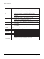
4-8-2(H) OPTION 2
Micom Spec : SIM-806MA
ITEM(OSD)
No.
1
Language
2
Sound
3
CRT
4
AV Mode
5
x-ray
6
Tilt Control
7
Auto FM
8
PIP
9
Txt Language
10
LNA
11
Equalizer
12
High deviate
13
TTX On/OFF
14
AV by CH Key
Samsung Electronics
Control
Arab
Iran
Libya
CIS
A2/NICAM
Virtual Dolby
Mono
Line-Stereo
4:3
Wide
Q(12.8:9)
4:3-16:9
Q - 16:9
1Scart
2Scart
2scart+S
1RCA
2RCA
2RCA+S
2RCA+D
2RCA+S+D
On
Off
On
Off
On
Off
Off
1- tuner
2 - tuner
West Europe
East Europe
TRussian
Greek-Turkey
Arabic
Farsi
Arab-Hebrew
On
Off
On
Off
On
Off
On
Off
On
Off
Description
English/Arab/French/Pakistan
English/Persian/French/Turkey
English/Libya/French
English/Russia
A2 Stereo / Nicam Stereo Model
Virtual Dolby Model
Mono Model
Line stereo Model
Normal / Zoom / 16:9
Wide CRT ( 16:9 )
Plus / Normal / Zoom / 16:9
Normal / Zoom
Plus / Normal / Zoom
Built in 1 Scart Model
Built in 2 Scart Model
Built in 2 Scart +SVHS JACK Model
Built in RCA 6P / RCA 4P Model
Built in RCA 9P Model
Built in RCA 9P + SVHS JACK Model
Built in RCA 9P + DVD JACK Model
Built in RCA 9P + SVHS JACK Model + DVD JACK Model
X-ray detection function on
X-ray detection function off
CRT Tilt control function on ( wide / 29PF CRT)
CRT Tilt control function off
automatic change from NICAM to FM depends on NICAM error rate
automatic change from NICAM to FM depends on NICAM syncronization
no PIP function
1 Tuner PIP function
2 Tuner PIP function
English/German/Skandinavian/Italian/French/Spainsh/Czech
Polish/Czech/Rumanian/Slovenian/Croatian/
French/Skandinavian/German/Italian
Russian/Ukranian/Estonian/Czech/German/Lettish/English
English/Turkey/Greek/French/Skandinavian/German/Spainsh/Italian
English/Arabic/French
English/Farsi/French
Arabic/Hebrew
Built in LNA Tuner
Built in Normal Tuner
Include in Equalizer function ( MSP34X0D)
Without Equalizer function (MSP34X5D)
High deviation mode on MSP34XX
Normal mode on MSP34XX
TTX Model
W/O-TTX Model
Without Video Pannel Key
With Video Pannel Key
4-17
Alignment and Adjustments
4-8-2(I) OPTION 3
Micom Spec : SIM-806EI/SIM-806C
No.
1
ITEM(OSD)
SOUND
2
CRT
Control
Description
A2/NICAM
Virtual Dolby
Mono
Line-Stereo
4:3
Wide
Q(12.8:9)
4:3-16:9
Q - 16:9
1Scart
2Scart
2scart+S
1RCA
2RCA
2RCA+S
2RCA+D
2RCA+S+D
On
Off
On
Off
On
Off
Off
1 - tuner
2 - tuner
On
Off
On
Off
On
Off
A2 Stereo / Nicam Stereo Model
Virtual Dolby Model
Mono Model
Line stereo Model
Normal / Zoom / 16:9
Wide CRT ( 16:9 )
Plus / Normal / Zoom / 16:9
Normal / Zoom
Plus / Normal / Zoom
Built in 1 Scart Model
Built in 2 Scart Model
Built in 2 Scart +SVHS JACK Model
Built in RCA 6P / RCA 4P Model
Built in RCA 9P Model
Built in RCA 9P + SVHS JACK Model
Built in RCA 9P + DVD JACK Model
Built in RCA 9P + SVHS JACK Model + DVD JACK Model
X-ray detection function on
X-ray detection function off
CRT Tilt control function on ( wide / 29PF CRT)
CRT Tilt control function off
automatic change from NICAM to FM depends on NICAM error rate
automatic change from NICAM to FM depends on NICAM syncronization
no PIP function
1 Tuner PIP function
2 Tuner PIP function
Built in LNA Tuner
Built in Normal Tuner
Include in Equalizer function ( MSP34X0D)
Without Equalizer function (MSP34X5D)
High deviation mode on MSP34XX
Normal mode on MSP34XX
3
A/V Mode
4
x-ray
5
Tilt Control
6
Auto FM
7
PIP
8
LNA
9
Equalizer
10
High deviate
11
AKB
On
Off
AKB Function On
AKB Function Off
12
AV by CH Key
On
Off
Without Video Pannel Key
With Video Pannel Key
13
Woofer
On
Off
Woofer Function ON
Woofer Function OFF
India only
4-18
Samsung Electronics
Alignment and Adjustments
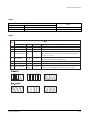
4-8-2(J) G2 - ADJUSTMENT
❑ When using RGB AMP STV-5109
CRT
G2 ADJUST
RANGE
TSB 21-FLAT
LG-CPT 21-FLAT
SDI 21" FALT
SDI 14"
SDI 15" FLAT
A51LSH196X03(+380)
A51QDJ279X14 A51QDX991X001 A34KQV42X A36QDT351X
A51LSH198X03(-250)
MRC R G B
MRWDG
IBRM
WDRV
CDL
COL R G B
COL G
COL B
NO CONTROL
NO CONTROL
0~255
0~255
0~255
0~255
0~255
0~255
110
110
225
45
185
75
75
75
110
110
220
35
200
145
145
145
110
110
225
45
175
165
165
165
110
110
205
45
100
100
100
100
110
110
215
45
160
80
80
80
CRT
G2 ADJUST
RANGE
SDI 21" 1.7R
SDI 25" 1.3R
SDI 25" FLAT
A51KQJ63X01 A59KPR84X01 A59QDF891X002
MRC R G B
MRWDG
IBRM
WDRV
CDL
COL R G B
COL G
COL B
Samsung Electronics
NO CONTROL
NO CONTROL
0~255
0~255
0~255
0~255
0~255
0~255
110
110
215
45
160
80
80
80
110
110
210
35
220
130
130
130
110
110
205
45
150
140
140
140
SDI 29" 1.3R
SDI 30"
A68QBT891X002 A70QBZ791X001
A68KVL74X01
110
110
200
45
190
150
150
150
110
110
200
45
180
130
130
130
4-19
Alignment and Adjustments
❑ When using RGB AMP TDA6101Q
CRT
G2 ADJUST
RANGE
TSB 21-FLAT
LG-CPT 21-FLAT
SDI 21" FALT
SDI 14"
SDI 15" FLAT
A51LSH196X03(+380)
A51QDJ279X14 A51QDX991X001 A34KQV42X A36QDT351X
A51LSH198X03(-250)
MRC R G B
MRWDG
IBRM
WDRV
CDL
COL R G B
COL G
COL B
0~255
0~255
0~255
0~255
0~255
0~255
0~255
0~255
110
110
220
35
230
65
65
65
110
110
220
35
230
65
65
65
110
110
230
35
230
65
65
65
110
110
180
35
100
100
100
100
110
110
220
35
200
150
150
150
CRT
G2 ADJUST
RANGE
SDI 21" 1.7R
SDI 25" 1.3R
SDI 25" FLAT
A51KQJ63X01 A59KPR84X01 A59QDF891X002
MRC R G B
MRWDG
IBRM
WDRV
CDL
COL R G B
COL G
COL B
G2-ADJUST
RANGE
MRC R G B
0~255
MRWDG
IBRM
WDRV
CDL
COL R G B
COL G
COL B
4-20
NO CONTROL
NO CONTROL
0~255
0~255
0~255
0~255
0~255
0~255
110
110
220
35
230
65
65
65
110
110
220
35
230
65
65
65
110
110
210
35
150
150
150
150
SDI 29" 1.3R
SDI 30"
A68QBT891X002 A70QBZ791X001
A68KVL74X01
110
110
220
35
180
65
65
65
110
110
210
35
160
130
130
130
DESCRIPTION
Measure of Cutoff Gain, the data comes when adjusting the screen voltage. It is set to the point
where changing red into green. RGB Output. By sending the standard pulse data, it receives
feedback from RGB drive. It is low light data.
Measure of Green of Drive Gain, the data that indicates the value of High Light. It has the same
0~255
principle as MRC R G B
Internal brightness measurement. For AKB, an 1-chip sends RGB standard pulse and sets
0~255
the level of the standard pulse.
White drive measure control. IBRM is the standard pulse of low light. WDRV is the standard
0~255
pulse of high light.
Cathode drive level. Sets the standard luminance of high light different by CRT and inch.
0~255
This uses the same register as the RED//GREEN/BLUE drive in video adjust-1.
Cutoff level R. Uses the same register as the RED cutoff in Video adjust-1.
0~255 Cutoff level G. Uses the same register as the GREEN cutoff in Video adjust-1.
Cutoff level B. Uses the same register as the BLUE cutoff in Video adjus
Samsung Electronics
Alignment and Adjustments
4-8-2(K) OTHERS
Application CRT
OTHERS
RANGE
TSB CPT 21-FLAT
LG-CPT 21-FLAT
SDI 21" FALT
SDI 15" FLAT SDI 21" 1.7R
A51LSH196X03(+380)
A51QDJ279X14 A51QDX991X001 A36QDT351X A51KQJ63X01
A51LSH198X03(-250)
VSU (VDP3130Y)
(VDP3112B)
H QEW
H ZOOM Parabola
H 16:9 Parabola
TTX H Shift
Mono Sound System
V Slice Level
Melody Volume
AKB
TTX LIST PRIOR
96~111
-30~30
-30~30
-30~30
-30~30
BG
0~3
0~20
ON/OFF
ON/OFF
100
100
0
8
-10
0
BG
2
5
ON
OFF
100
110
0
8
-18
0
BG
2
5
ON
100
110
0
8
-18
0
BG
2
5
ON
100
108
0
25
-30
0
BG
2
5
ON
98
108
0
8
-10
0
BG
2
5
ON
Application CRT
OTHERS
VSU (VDP3130Y)
(VDP3112B)
H QEW
H ZOOM Parabola
H 16:9 Parabola
TTX H Shift
Mono Sound System
V Slice Level
Melody Volume
AKB
TTX LIST PRIOR
Samsung Electronics
RANGE
96~111
-30~30
-30~30
-30~30
-30~30
BG
0~3
0~20
ON/OFF
ON/OFF
SDI 25" 1.3R
SDI 25" FLAT
SDI 29" 1.3R
SDI 30"
A59KPR84X01
A59QDF891X002
A68QBT891X002
A68KVL74X01
A70QBZ791X001
98
108
0
0
0
0
BG
2
5
OFF
100
100
0
-12
0
0
BG
2
5
ON
98
108
0
0
-10
0
BG
2
5
OFF
110
110
-7
-10
0
0
BG
2
5
OFF
4-21
Alignment and Adjustments
OTHERS
RANGE
DESCRIPTION
Vertical Setup Time. Delays the vertical sync to solve the jitter of OSD and TTX .
Check OSD while varying 96 111 step by step and an 1H line moves at two points.
If the value is set at the first point or second point, an OSD jitter may happen. Also,
if the value is set between the first and second points, a TTX jitter may happen.
VSU
96~111 So, the value of VSU should be set after giving some magines (three steps).
For example, OSD moves as much as 1H-line when changing data 98 to 99 and 106 to 107,
respectively.
At this time, VSU should be set to 110 by allowing for the margin of three steps
(If the value within 99 to 106 is set, a jitter may happens in TTX mode.)
Short for Q-CRT HORIZNOTAL EAST WEST, data used only for Q-CRT MODEL.
In NORMAL mode, the horizontal picture size is within 5 5.5.
H QEW
-30~30
In Q mode, the horizontal picture size is within 6.5 7. This H QEW function sets the gap
between horizontal picture size in NORMAL mode and horizontal picture size in Q mode.
Corrects the vertical linearity in Zoom mode of P-SIZE. The data differs according to CRT
H ZOOM Parabola
-30~30
(see data above)
Corrects the vertical linearity in 16:9 mode of P-SIZE. The data differs according to CRT
H 16:9 Parabola
-30~30
(see data above).
Horizontal blanking pulse duty determines the position of TTX and FBT determines
horizontal blanking pulse duty.
TTX H Shift
-30~30
Because FBT depends on model, this TTX H Shift allows the micom to set the start
position of pixel to prevent the TTX screen from being shifted.
Mono Sound System
Not Used
BG
V Slice Level
0~3
Melody Volume
0~20
AKB
ON/OFF
TTX LIST PRIORITY
ON/OFF
4-22
Allows the sync slice level of sync separate block to be changed. This item corresponds the case
where a vertical bouncing happens according to signal conditions by area
(overmodulation, especially). 0: 100% 1: 90% 2: 75% 3: 60%
Sets the level of melody volume in Picture ON. Differently controlled according to buyer and area.
Short for Auto Kined Bias, a function that maintains uniformity in brightness and white balance by
automatically correcting the variance of brightness and white balance according to temperature
and characteristics of AMP in the CRT drive. It is designed to be turned ON/OFF so that the AKB
line can't be seen at top when a DY of lower deflection sensitivity is used
TTX mode has two different types; List and FLOF. When swtiching into the TTX mode, this function
determines which type has priorty.
Samsung Electronics
Alignment and Adjustments
Table 5.
VDP Version
OSD
B
Y
Description
Chroma IC is VDP3108B/VDP3112B/VDP3120B
Chroma IC is VDP3130Y/VDP3130Y-B2
Remark
Normal Version IC
DVD Version IC
Table 6.
Y-ADD
NO
1
2
3
4
5
6
7
8
FUNCTION
RANGE INITIAL VALUE
-128~127
0
Horizontal bow control: Actually doesn't operate (see figure blow)
-128~127
0
Horizontal angle control: Actually doesn't operate (see figure below)
1~7
2
Discharge sample counter for deflection retrace
Determines the presence of use of DVD SUB TINT control.
0~1
1
When VDP3130Y B1 is used, it is set to1 and When VDP3130Y B2
DVD TINT CONTROL
is used, it is set to 0.
After the NTSC DVD signal is input, this function set a proper phase
0~100
25
DVD SUB TINT
in Picture Standard mode. Initial Value = 25
EHT Compensation east/west offset coefficent (Not used)
EHT OFFSET
0~535
0
EHT Compensation east/west gain coefficent (Not used)
EHT HORIZONTAL -128~127
0
Switches VDP3130Y IC version On/Off. When VDP3130Y B2-version
VDPY B2-VERSION
ON
is used, it is set ON. When B1-version is used, it is set OFF.
ON/OFF
ITEM(OSD)
H BOW
H ANGLE
H DSCC
Samsung Electronics
4-23
Alignment and Adjustments
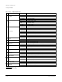
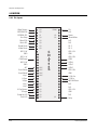
4-9 MICOM
4-9-1 Pin Layout
Write Protect
EEPROM SDA
EEPROM SCL
Bus-Stop
Main SDA
Main SCL
Sound Reset
Video Reset
VDD 2.5V
GND
VDD 3.3V
CVBS Input
VDD 2.5V
GND
AFT
Scart1 Ident
Scart2 Ident
Key 1
H-Sync
V-Sync
Key 3
Key 2
X-Ray Protect
IR Input
Stand-By LED
Time LED
4-24
1
I/O
2
I/O
3
IO
I/O
50
4
I/O
I/O
49
5
I/O
48
6
I/O
47
7
I/O
46
8
I/O
45
9
10
11
12
13
14
15 ADC
16 ADC
PWM
52
51
44
S
D
A
5
5
5
X
43
42
41
40
39
38
37
17 ADC
36
18 ADC
35
19
34
20
33
21 I/O
32
22 I/O
31
23 I/O
30
24 I/O
29
25 I/O
28
26 I/O
I/O
27
Tilt
N.C.
Power
Sound Mute
N.C.
N.C.
PX. Y
PX. Y
VDD 3.3V
GND
VDD 2.5V
CORE
OSD-B
OSD-G
OSD-R
VDD 2.5V
GND
X-TAL Out
X-TAL In
MICOM Reset
N.C.
N.C.
VDD 3.3V
GND
N.C.
Relay
Samsung Electronics
Alignment and Adjustments
4-9-2 Pin Assignment Specification
PIN NO FUNCTION
ASSIGN
IN/OUT
ACTIVE H/L
Out
Low
DESCRIPTION
1
I/O
Write Protect
2
I/O
ROM SDA
I/O
EEPROM Serial Data Line
3
I/O
ROM SCL
I/O
EEPROM Serial Clock Line
4
I/O
Bus Stop
In
5
I/O
Main SDA
I/O
6
I/O
Main SCL
I/O
Low
Peripheral IC Serial Clock Line
7
I/O
Sound Reset
Out
Low
MSP IC Initial Control
8
I/O
Video Reset
Out
VDP IC Initial Control
9
Vdd
VDD 2.5V
10
GND
11
Vdd
VDD 3.3V
12
CVBS
CVBS Input
In
TTX CVBS Input
13
Vdd
VDD 2.5V
14
GND
15
ADC
AFT
In
Auto Fine Tuning Control
16
ADC
SC1-ID
In
Scart1 Ident
17
ADC
SC2-ID
In
Scart2 Ident
18
ADC
Key1
In
Key1 Input
19
HS
H-Sync
In
Horizontal Sync Input
20
VS
V-Sync
In
Vertical Sync Input
21
I/O
Key3
In
Key3 Input
22
I/O
Key2
In
Key2 Input
23
I/O
X-Ray
In
X-Ray Protection
24
I/O
IR-In
In
Remocon Signal Input
25
I/O
STD-LED
Out
LED Drive Output(Red)
26
I/O
TIM-LED
Out
LED Drive Output(Green)
Samsung Electronics
Low
EEPROM Write Protection
Disable Micom IIC
Peripheral IC Serial Data Line
Analog B+
Analog Ground
4-25
Alignment and Adjustments
4-9-2 Pin Assignment Specification (Continued)
PIN NO FUNCTION
ASSIGN
IN/OUT
ACTIVE H/L
Out
Low
DESCRIPTION
27
I/O
28
N.C.
Not Used (Programmed Gound Level)
29
GND
Analog Ground
30
Vdd
31
N.C.
Not Used (Programmed Gound Level)
32
N.C.
Micom Hardware Reset
33
Reset
Reset
In
Low
Crystal Oscillation Input
34
X-In
X-TAL In
In
6MHz
Crystal Oscillation Output
35
X-Out
X-TAL Out
Out
6MHz
Analog Ground
36
GND
37
Vdd
VDD 2.5V
38
R
OSD-R
Out
OSD/TTX Output (Green)
39
G
OSD-G
Out
OSD/TTX Output (Blue)
40
B
OSD-B
Out
Fast Blank/Half Contrast Output
41
COR
CORE
Out
42
Vdd
VDD 2.5V
43
GND
44
Vdd
VDD 3.3V
45
I/O
PX.Y
In
46
I/O
PX.Y
Out
47
N.C.
48
N.C.
49
I/O
S-Mute
Out
High
Sound Amp Mute
50
I/O
Power
Out
Low
Picture On/Off Control
51
N.C.
52
I/O
Relay
Activate Degausssing Coil
Not Used (Programmed Gound Level)
VDD 3.3V
Analog B+
OSD/TTX Output (Red)
When The Caption Function Adopted, Used.
Not Used (Programmed Gound Level)
4-26
Not Used (Programmed Gound Level)
Samsung Electronics
Troubleshooting
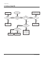
5. Troubleshooting
5-1 No Power
Disconnect
the Power Cord
Check/Replace
IC803, 805
Abnormal
LED ON
Check
Power LED
LED OFF
Check IC908 and
Replace IC901
Check
the voltage of
IC803, 805
Normal
Abnormal
Normal
Check
Q909, Q910
Normal
Check IC901
Pin 50
Abnormal
Normal
Check
IC901 B+
Normal
Check IC901
Pin 5 6
Abnormal
Check
H-OUT of IC201
Pin 50
Abnormal
Abnormal
Check
the voltage of
IC804
Abnormal
Check
the resistance of
FD803
Normal
Check
IC803
Replace
Q909,Q910
Normal
Abnormal
Check
IC803
Replace
IC902
Abnormal
Replace
IC201
Check
IC902
Normal
Check
SCL, SDA Line
Abnormal
Check Q401 and
Horizontal Circuit
Normal
Check the
voltage of
IC803, 805
Normal
Check FBT and
B+(130V)
Replace FD803
Check
IC801, D801 FUSE
Samsung Electronics
5-1
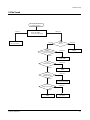
Troubleshooting
5-2 No Raster (Sound OK)
No Raster
(Sound OK)
Check
Fusible Resistance
Check
the fusible resistance
of abnormal volatge line
Abnormal
Abnormal
Check
voltage of
heater
Normal
Check
Abnormal
RK,GK,BK Signal
output from
CRT PCB
Normal
Abnormal
Check
CRT and FBT
Abnormal
Check
the signal output
from IC201 Pin
63
Normal
Check / Replace
IC201
5-2
Check
R.G.B Signal
input to CRT PCB
Abnormal
Check tuner B+
and Main CVBS
Check
R.G.B Signal
Output from
IC201
Normal
Check
B+
(200V, 16V)
Normal
Check
Q501 and re-adjust
Screen Voltage
Normal
Check
Q202, Q203, Q204,
Q207, Q209, Q213,
Q206, Q208, Q210
Samsung Electronics
Troubleshooting
5-3 No Sound
No Sound, but Picture is
in normal operation
Normal
Check the Speaker
Wire Connection
Abnormal
Check the CN602
Connection and Signal
Normal
Check
IC602 #7
(If the pin is in low state,
Sound is mute)
Check
14V Line
Abnormal
Abnormal
Check
FA803S
Normal
Check
D816, Q906
Check
IC601 #24, #25
Abnormal
Normal
Replace
IC602
Check
IC601 Input
Voltages (5V,8V)
Abnormal
Normal
Check
the coils around IC601
Check
IC601 Input Signal
Abnormal
Normal
Replace
IC601
Samsung Electronics
Check
the Tuner
5-3
Troubleshooting
5-4 Horizontal Lines Appear on screen
Horizontal Lines
Apper on screen
Normal
Normal
Check
the VDP Signal
output from IC201
Pin 31
Check
IC301 B+
(16V, -16V)
Abnormal
Check
B+ Line and the fusible
resistance of R425, 424
Abnormal
Check/Replace
IC301
5-4
Check
IC201
Samsung Electronics
Exploded View & Parts List
6. Exploded View & Parts List
6-1 CS21S8NAS/MUR
No
Samsung Electronics
Code No
Description;Specification
Q’ty
Remark
1
AA64-02233A
CABINET-BACK;21S8,HIPS,HB,G4309
1
1-1
AA64-70123B
BADGE-BRAND;ALL,AL,8.5,L50,BLK,SILVER,SA
1
1-2
AA64-02235B
KNOB POWER;21S8,ABS,HB,G3676,GDM3130
1
1-3
AA61-60003J
SPRING ETC-CS;-,SUS304,-,-,OD6,N7,OD6,-,
1
1-4
AA64-02234B
DECORATION-CONTROL;21S8,HIPS,HB,G4309,GD
1
1-5
AA64-02237A
WINDOW-RMC,LED;21S8,ACRYL,CLR
1
1-6
AA64-02239D
DECORATION-TWEETER,R;21S8 NEW,HIPS,HB,G4
1
1-7
AA65-00011C
CLAMPER CORE-WIRE;ALL MODEL,NYLON 66,V2,
1
1-8
AA61-40113A
STOPPER-PCB;501H,HIPS,-,-,HB,NTR,-
1
1-9
AA95-01784V
ASSY SUB-PCB,A/V FRONT;DP,21A8,KS2AAA95-
1
1-10
6006-001095
SCREW-ASS’Y TAPT;WP,BH,+,M4,L12,ZPC(YEL)
2
1-11
AA64-02236B
KNOB CONTROL;21S8,ABS,HB,G3676,GDM3130
1
1-12
6003-001026
SCREW-TAPTITE;RH,+,B,M4,L15,ZPC(BLK),SWR
1
1-13
AA91-00862B
ASSY HOLDER SPK;,4OHM,µø≥≤æ∆SOUND∞≠¡∂«‹,
2
1-14
6003-001019
SCREW-TAPTITE;RH,+,B,M4,L12,ZPC(BLK),SWR
2
1-15
AA61-00870B
HOLDER-TWEETER;21S8,HIPS HB,G4309,SV012P
2
1-16
AA64-02238B
GRILLE-TWEETER;21S8,SECC,T0.5,GDM-S130
2
1-17
6003-001019
SCREW-TAPTITE;RH,+,B,M4,L12,ZPC(BLK),SWR
2
1-18
AA91-00861B
ASSY HOLDER SPK;,8OHM,15W,21S8
1
1-19
6002-000512
SCREW-TAPPING;RH,+,2,M4,L12,ZPC(BLK),SWR
4
2
AA03-00302A
CRT COLOR;A51QDX992X001(NF),+380MG,1.85M
1
2-1
AA65-00009B
CLAMPER CORE-D,COIL;21A8,NYLON 66,V0,-,-
4
D-COIL
2-2
AA60-10050R
SCREW-ASSY;-,SWRCH18A,M5,L31.5,HH,+,WC,-
4
CRT+CF
2-3
3704-001105
SOCKET-CRT;11P,20PI,26.5PI,NI,-
1
V999S
3
AA64-02647D
CABINET BACK;DP,21S8,HB,AA64-02233A(12KG
1
3-1
AA60-10050T
SCREW-TAPPING;-,SWRCH18A,M4,L20,RH,+,2S,
6
3-2
AA42-00003A
ANT ROD;-,3S,720mm,ABS,UL/CSA,-
1
3-3
AA96-00697A
ASSY POWER CORD;,KKP419C,CP2/NO(4.0),H/C
1
S.N.A
KNOPOW
AV+CF
T0081
T0081
SPK+HT
SPK+HT
CB+CF
6-1
Electrical Parts List
You can search for the updated part code through ITSELF web site.
URL : http://itself.sec.samsung.co.kr
7. Electrical Parts List
7-1 CS21S8NAS/MUR
Level Loc. No. Code No.
Description ; Specification
ASSY COVER REAR
1
AA90-02009W ASSY COVER REAR;CS21S8NAS/MUR
2
2
2
3
3
3 800
3
3
3
3
AA60-00091J
AA64-00892F
AA64-02647D
0203-001269
AA64-02233A
AA69-01410A
AA69-01559U
AA69-01897D
AA69-01897E
AA69-01948A
SPACER-FELT;-,FELT,330X10,-,-,BLK,T0.5,INLAY-BACK;D2,D3,PS SHEET,T0.3,-,-,BLK,R
CABINET BACK;DP,21S8,HB,AA64-02233A(12KG
TAPE-OPP MASKING;#301,T0.06,W75,L50000,N
CABINET-BACK;21S8,HIPS,HB,G4309
MASTER CARTON;,CB DW-3,100,100,100,YEL
PAD;,PS,660,475,T18
BAG-VINYL;,HDPE T0.02,1400,1400
BAG-VINYL;,HDPE T0.02,1400,2100
PAD-TYPE;,SW-2,805,625
ASSY COVER FRONT
1
2
2
2
2
2
2
2
2
2
2
3
3
3
3
2
2
2
2
3
3
2
3
3
3
3
3
3
3
3
3
3
3
3
4
4
4
4
4
4
3
4
4
4
AA90-04489J ASSY COVER FRONT;CS21S8NAS/MUR
C/F
SPK+HT
CF+KC
HTW+CF
SPK+CF
AV+CF
CRT+CF
CB+JAC
CB+CF
0203-001290
6002-000512
6002-000514
6002-000522
6006-001095
6006-001095
AA60-10050R
AA60-10050T
AA60-10050T
AA64-02670A
0203-001269
AA64-02236B
109
AA69-01402A
468
AA69-01410A
D-COIL
AA65-00009B
AA91-00861B
AA91-00862B
AA91-00983A
AA61-00870B
AA64-02238B
AA91-01008A
FRONT
0203-001085
AA60-00091F
AA61-40113A
KNOPOW AA61-60003J
AA64-02668B
AA64-02234B
AA64-02235B
AA64-02237A
AA64-70123B
AA65-00011C
AA65-30105C
AA64-02671B
0203-001269
AA61-01109H
BOX
AA63-70002A
AA64-02239C
166
AA69-01401A
811
AA69-01410A
AA64-02671C
0203-001269
AA61-01109H
BOX
AA63-70002A
Samsung Electronics
TAPE-OPP MASKING;ANT 100C,T0.073,W30,L50
SCREW-TAPPING;RH,+,2,M4,L12,ZPC(BLK),SWR
SCREW-TAPPING;RH,+,2,M4,L15,ZPC(BLK),SWR
SCREW-TAPPING;TH,+,2,M4,L15,ZPC(BLK),SWR
SCREW-ASS’Y TAPT;WP,BH,+,M4,L12,ZPC(YEL)
SCREW-ASS’Y TAPT;WP,BH,+,M4,L12,ZPC(YEL)
SCREW-ASSY;-,SWRCH18A,M5,L31.5,HH,+,WC,SCREW-TAPPING;-,SWRCH18A,M4,L20,RH,+,2S,
SCREW-TAPPING;-,SWRCH18A,M4,L20,RH,+,2S,
KNOB CONTROL;DP,21S8,AA64-02236B
TAPE-OPP MASKING;#301,T0.06,W75,L50000,N
KNOB CONTROL;21S8,ABS,HB,G3676,GDM3130
PAD-PLATE;,CB DW-2,YEL,100,100
MASTER CARTON;,CB DW-3,100,100,100,YEL
CLAMPER CORE-D,COIL;21A8,NYLON 66,V0,-,ASSY HOLDER SPK;,8OHM,15W,21S8
ASSY HOLDER SPK;,4OHM,µø≥≤æ∆SOUND∞≠¡∂«‹,
ASSY-HOLDER TWEETER;DP,HB G4309,SV012P,2
HOLDER-TWEETER;21S8,HIPS HB,G4309,SV012P
GRILLE-TWEETER;21S8,SECC,T0.5,GDM-S130
ASSY CABINET FRONT;DP,21S8 PAL,SV012P+GD
TAPE-DOUBLE FACE;#4929,T0.64,W12,-,BLK
SPACER-FELT;-,FELT,150X10,-,-,BLK,T0.5,STOPPER-PCB;501H,HIPS,-,-,HB,NTR,SPRING ETC-CS;-,SUS304,-,-,OD6,N7,OD6,-,
CABINET-FRONT;DP,21S8,AA64-02232D
DECORATION-CONTROL;21S8,HIPS,HB,G4309,GD
KNOB POWER;21S8,ABS,HB,G3676,GDM3130
WINDOW-RMC,LED;21S8,ACRYL,CLR
BADGE-BRAND;ALL,AL,8.5,L50,BLK,SILVER,SA
CLAMPER CORE-WIRE;ALL MODEL,NYLON 66,V2,
CLAMPER CORE-WIRE;ALL MODEL,NYLON 66,V2,
DECORATION-TWEETER,L;DP,21S8,AA64-02239C
TAPE-OPP MASKING;#301,T0.06,W75,L50000,N
CASE-PP BOX;,PP,385,310,35
SHEET;-,PE FOAM,T1.0,-,-,-,50G
DECORATION-TWEETER,L;21S8 NEW,HIPS,HB,G4
PAD-PLATE;,CB SW-2,YEL,100,100
MASTER CARTON;,CB DW-3,100,100,100,YEL
DECORATION-TWEETER,R;DP,21S8,AA64-02239D
TAPE-OPP MASKING;#301,T0.06,W75,L50000,N
CASE-PP BOX;,PP,385,310,35
SHEET;-,PE FOAM,T1.0,-,-,-,50G
Remark
Level Loc. No. Code No.
4
4 166
4 811
Description ; Specification
Remark
AA64-02239D DECORATION-TWEETER,R;21S8 NEW,HIPS,HB,G4
AA69-01401A PAD-PLATE;,CB SW-2,YEL,100,100
AA69-01410A MASTER CARTON;,CB DW-3,100,100,100,YEL
ASSY CHASSIS
1
2
3
3
4
4
4
4
4
4
4
4
4
4
4
4
4
4
4
4
4
4
4
4
4
4
4
4
4
4
4
4
4
4
4
4
4
4
4
4
4
4
4
4
4
4
4
4
4
4
4
4
4
5
5
5
AA91-06212H ASSY CHASSIS;,KS2A
AA91-06904A ASSY MISC-CHASSISPACK;2
AA68-02713A LABEL-AUTO;A/P,15,35,WHITE,ALL MODEL
AA94-12299J ASSY PCB MAIN;,KS2A
0202-000008 SOLDER-WIRE;S63S-W3.0,S63S,D3,63Sn/37Pb,
0202-000187 SOLDER-WIRE FLUX;-,RS60S,D1.2,63Sn/37Pb
0202-000188 SOLDER-BAR;S63S-B20,S63A,22x335,63Sn/37P
0204-000441 FLUX;JS95TVS,FLUX,20,0204-000442 SOLVENT;1M-1000,C3H70H,96,D813
0402-000233 DIODE-RECTIFIER;FML-G12S,200V,5A,-,D801S
0402-001160 DIODE-BRIDGE;D5SB60,600V,6A,SIP-4,DH02
0402-001296 DIODE-RECTIFIER;FMP-3FU,1.5KV,5A,TO-3PF,
DH01
0502-001136 TR-POWER;KSD5703,NPN,70W,TO-3PF,ST,8PC801S 0604-001038 PHOTO-COUPLER;TR,130-260%,200mW,DIP-4,ST
IC902
1103-001177 IC-EEPROM;24WC16,2048x8Bit,DIP,8P,-,-,2.
IC803
1203-002085 IC-VOLTAGE REGULATOR;78R08,TO-220,4P,-,P
IC201S
1204-001812 IC-VIDEO PROCESS;VDP3130Y-B2,DIP,64P,760
IC601
1204-002038 IC-SOUND PROCESSOR;MSP3410G-PO-83V3,PSDI
NT802S 1404-001045 THERMISTOR-NTC;4.7ohm,15%,2900K,35.0mW,T
P801S
1404-001156 THERMISTOR-PTC;9OHM,+30%/-20%,220VRMS,27
CY802S 2201-000446 C-CERAMIC,DISC;3.3NF,20%,400V,Y5U,BK,15X
C407
2301-001338 C-FILM,LEAD-OTHER;0.68NF,5%,1.6KV,BK,28X
CR402S 2301-001467 C-FILM,LEAD-PPF;3.9NF,3%,1.6KV,BK,29X8.X
CR401S 2301-001468 C-FILM,LEAD-PPF;3.3NF,3%,1.6KV,BK,29X13.
CX802S 2306-000318 C-FILM,LEAD-PPF;220NF,20%,250V,BK,-,22.5
CX801S 2306-000318 C-FILM,LEAD-PPF;220NF,20%,250V,BK,-,22.5
CR405S 2306-000350 C-FILM,LEAD-PPF;270NF,5%,400V,BK,26X18.5
C806
2401-001426 C-AL;470uF,20%,400V,GP,-,35x45mm,10
C815
2401-003633 C-AL;220UF,20%,160V,GP,ST,22X25MM,10
X201
2801-004019 CRYSTAL-UNIT;20.25MHz,30ppm,28-AAM,13pF,
X601
2801-004020 CRYSTAL-UNIT;18.432MHz,30ppm,28-AAM,12pF
SW801S 3403-001107 SWITCH-PUSH;250V,5A,DPST,-,KDC-A04
FP801S 3601-000281 FUSE-CARTRIDGE;250V,4A,TIME-LAG,GLASS,5.
V999S
3704-001105 SOCKET-CRT;11P,20PI,26.5PI,NI,JA701
3722-001333 JACK-PIN;9P,3.2mm,NI,BLK,JA702
3722-001596 JACK-PIN;3P/9P,3.5mm,NI,BLK(GRN/BLU/RED)
T801S
AA26-00044A TRANS SWITCHING;-,-,-,AC90~260V,DC135/15
T444S
AA26-00057A TRANS FBT;-,FUH-29A001B(S),25/29,130
T401
AA26-50001M TRANS-HORIZ.DRIVE;-,-,-,80mH,-,-,520uH,L808
AA27-00098A COIL CHOKE;-,-,24uH,10%,-,0.1,3.0A,DR10X
CR404S AA27-00147A COIL HORIZ. WIDTH;,170UH,BK,54T+2-2
LR401S AA27-00281A COIL LINEARITY;64UH,64UH,DR1215 C:4.5,7.
LX801S AA29-30002F FILTER LINE NOISE;-,6mH,2.45A,-,RM901 AA32-00015A MODULE REMOCON;FRP-3521H31,38KHZ,940MM,M
AA39-20010B LEAD CONNECTOR-ASSY;,1P,500,YFH800-01,S,
AA39-20010H LEAD CONNECTOR-ASSY;,1P,300,YFH800-01,S,
CN502B AA39-20053A LEAD CONNECTOR-ASSY;,5P,400,YBNH025-05,S
CN501B AA39-20054B LEAD CONNECTOR-ASSY;,6P,500,YBNH025-06,S
TU01S
AA40-00082A TUNER;TCPS3001PD16D(S),PAL-M(NTSC),181CH
GT301
AA60-40012D PIN-GT,ASSY;T1.6,6-12.5-,NYLON66
AA61-00707B HOLDER-COVER;ALL MODEL,NYLON-66 T1.0 V2,
AA68-02713A LABEL-AUTO;A/P,15,35,WHITE,ALL MODEL
IC804
AA96-00243C ASSY H/S;-,REGULATOR,AA62-00045A,KA7806,
1203-000284 IC-POSI.FIXED REG.;7806,TO-220,3P,-,PLAS
6003-000335 SCREW-TAPTITE;RH,+,2S,M3,L8,ZPC(YEL),SWR
AA62-00065A HEAT SINK-PS;DP,-,-,-,AA62-00045A,-,-,-,
7-1
Electrical Parts List
Level Loc. No. Code No.
4
4
5
5
5
5
5
5
4
5
5
5
4
5
5
5
5
5
4
5
5
5
4
5
5
5
4
5
5
5
5
5
5
5
5
5
5
5
5
5
5
5
5
5
5
5
5
5
5
5
5
5
5
5
5
5
5
5
5
5
5
5
5
5
5
5
5
5
5
5
5
5
5
5
5
5
7-2
LD901
DDR01
IC501
IC801S
IC602
IC301
CIS
CIS
CIS
D201
D202
D207
D208
D209
D210
D212
D501
D502
D503
D508
D602
D604
D804
D906
D908
DZ402
D403
D406
D504
D810
D811
D907
D407
D413
D401
D402
D301
D411
D803
D816
D801
DZ201
DZ203
DZ204
DZ601
DZ602
DZ802
DZ806
DZ901
DZ902
DZ903
DZ904
DZ905
DZ906
DZ907
DZ908
DZ306
DZ804
AA96-00461A
AA96-00469F
0205-000129
0402-001358
0402-001375
1203-001006
6003-000334
AA62-00053B
AA96-00582A
1201-001687
6003-000334
AA62-00096A
AA96-50373F
0205-000129
6003-000335
AA13-00101A
AA61-10386A
AA62-30181K
AA96-50398A
1201-001064
6003-000335
AA62-30182E
AA96-50406G
1204-001807
6003-000333
AA62-00058A
AA97-04058A
0401-000005
0401-000005
0401-000005
0401-000005
0401-000005
0401-000005
0401-000005
0401-000005
0401-000005
0401-000005
0401-000005
0401-000005
0401-000005
0401-000005
0401-000005
0401-000005
0401-000005
0402-000132
0402-000132
0402-000132
0402-000132
0402-000132
0402-000132
0402-000493
0402-000537
0402-000540
0402-000540
0402-000546
0402-000546
0402-000546
0402-000546
0402-001111
0403-000508
0403-000508
0403-000508
0403-000508
0403-000508
0403-000508
0403-000508
0403-000508
0403-000508
0403-000508
0403-000508
0403-000508
0403-000508
0403-000508
0403-000508
0403-000700
0403-000700
Description ; Specification
Remark
ASSY LED GUIDE;-,-,SL-255D,RED/GRN
ASSY H/S;-,REGULATOR,AA62-00053B,D10U60S
GREASE-SILICON;SC102,JAPAN
DIODE-RECTIFIER;FFPF10U60S,600V,10A,TO-2
DIODE-RECTIFIER;FFPF10U20S,200V,10A,TO-2
IC-VOLTAGE REGULATOR;78R05,TO-220F,4P,-,
SCREW-TAPTITE;RH,+,2S,M3,L6,ZPC(YEL),SWR
HEAT SINK;DREAM (D2,D3),AL ,T1.0,147,50,
ASSY H/S;-,CRT,AA62-00096A,STV5109,KS1A
IC-VIDEO AMP;STV5109,ZIP,15P,-,SINGLE,50
SCREW-TAPTITE;RH,+,2S,M3,L6,ZPC(YEL),SWR
HEAT SINK;KS2A,AL5052,T1.0,W36.0,H35.0,S
ASSY H/S;-,PWM,AA62-30181K,KA3A1265RD,IC
GREASE-SILICON;SC102,JAPAN
SCREW-TAPTITE;RH,+,2S,M3,L8,ZPC(YEL),SWR
IC HYBRID;KA3S1265RD,CN5039,5PIN,-50TO12
BRACKET-IC;100,SECC,T1.0,KA2S0680
HEAT SINK-ES;-,AL6063 EXTR.,2,WHT,40MM,ASSY H/S;-,-,AA62-30182E,TDA7297,IC-POWER AMP;7297,ZIP,15P,-,DUAL,32dB,PL
SCREW-TAPTITE;RH,+,2S,M3,L8,ZPC(YEL),SWR
HEAT SINK-ES;-,A6063 EXTR,-,WHT,-,-,-,40
ASSY H/S;,POWER,AA62-30180K,K57A
IC-VERTICAL PROCESSO;LA7841,SIP,7P,708MI
SCREW-TAPTITE;RH,+,2S,M3,L10,ZPC(YEL),SW
HEAT SINK-ES;DP,-,-,-,AA62-30180K,-,-,-,
ASSY AUTO-MAIN;CS21A9WAX/MUR,KS2A,MYANMA
DIODE-SWITCHING;1N4148,100V,200mA,DO-35,
DIODE-SWITCHING;1N4148,100V,200mA,DO-35,
DIODE-SWITCHING;1N4148,100V,200mA,DO-35,
DIODE-SWITCHING;1N4148,100V,200mA,DO-35,
DIODE-SWITCHING;1N4148,100V,200mA,DO-35,
DIODE-SWITCHING;1N4148,100V,200mA,DO-35,
DIODE-SWITCHING;1N4148,100V,200mA,DO-35,
DIODE-SWITCHING;1N4148,100V,200mA,DO-35,
DIODE-SWITCHING;1N4148,100V,200mA,DO-35,
DIODE-SWITCHING;1N4148,100V,200mA,DO-35,
DIODE-SWITCHING;1N4148,100V,200mA,DO-35,
DIODE-SWITCHING;1N4148,100V,200mA,DO-35,
DIODE-SWITCHING;1N4148,100V,200mA,DO-35,
DIODE-SWITCHING;1N4148,100V,200mA,DO-35,
DIODE-SWITCHING;1N4148,100V,200mA,DO-35,
DIODE-SWITCHING;1N4148,100V,200mA,DO-35,
DIODE-SWITCHING;1N4148,100V,200mA,DO-35,
DIODE-RECTIFIER;1N4004,400V,1A,DO-41,TP
DIODE-RECTIFIER;1N4004,400V,1A,DO-41,TP
DIODE-RECTIFIER;1N4004,400V,1A,DO-41,TP
DIODE-RECTIFIER;1N4004,400V,1A,DO-41,TP
DIODE-RECTIFIER;1N4004,400V,1A,DO-41,TP
DIODE-RECTIFIER;1N4004,400V,1A,DO-41,TP
DIODE-RECTIFIER;1R5GU41,400V,1.5A,DO-15L
DIODE-RECTIFIER;RH1A,600V,0.6A,DO-204AC
DIODE-RECTIFIER;RU20A,600V,1.5A,-,TP
DIODE-RECTIFIER;RU20A,600V,1.5A,-,TP
DIODE-RECTIFIER;TVR10G,400V,1.0A,DO-41,T
DIODE-RECTIFIER;TVR10G,400V,1.0A,DO-41,T
DIODE-RECTIFIER;TVR10G,400V,1.0A,DO-41,T
DIODE-RECTIFIER;TVR10G,400V,1.0A,DO-41,T
DIODE-RECTIFIER;1N5397GP,600V,1.5A,DO-20
DIODE-ZENER;MTZJ5.6B,5.6V,5.45-5.73V,500
DIODE-ZENER;MTZJ5.6B,5.6V,5.45-5.73V,500
DIODE-ZENER;MTZJ5.6B,5.6V,5.45-5.73V,500
DIODE-ZENER;MTZJ5.6B,5.6V,5.45-5.73V,500
DIODE-ZENER;MTZJ5.6B,5.6V,5.45-5.73V,500
DIODE-ZENER;MTZJ5.6B,5.6V,5.45-5.73V,500
DIODE-ZENER;MTZJ5.6B,5.6V,5.45-5.73V,500
DIODE-ZENER;MTZJ5.6B,5.6V,5.45-5.73V,500
DIODE-ZENER;MTZJ5.6B,5.6V,5.45-5.73V,500
DIODE-ZENER;MTZJ5.6B,5.6V,5.45-5.73V,500
DIODE-ZENER;MTZJ5.6B,5.6V,5.45-5.73V,500
DIODE-ZENER;MTZJ5.6B,5.6V,5.45-5.73V,500
DIODE-ZENER;MTZJ5.6B,5.6V,5.45-5.73V,500
DIODE-ZENER;MTZJ5.6B,5.6V,5.45-5.73V,500
DIODE-ZENER;MTZJ5.6B,5.6V,5.45-5.73V,500
DIODE-ZENER;TZP33A,33V,31-35V,1W,DO-41,T
DIODE-ZENER;TZP33A,33V,31-35V,1W,DO-41,T
Level Loc. No. Code No.
5
5
5
5
5
5
5
5
5
5
5
5
5
5
5
5
5
5
5
5
5
5
5
5
5
5
5
5
5
5
5
5
5
5
5
5
5
5
5
5
5
5
5
5
5
5
5
5
5
5
5
5
5
5
5
5
5
5
5
5
5
5
5
5
5
5
5
5
5
5
5
5
5
5
5
5
DZ701
DZ702
DZ803
DZ509
DZ305
DZ202
DZ801
DZ808
DZ501
DZ301
DZ302
DZ303
DZ304
D203
D204
D205
D206
D901
D902
D903
D904
D905
Q206
Q208
Q210
Q201
Q202
Q203
Q204
Q207
Q209
Q211
Q212
Q213
Q222
Q602
Q902
Q903
Q904
Q905
Q906
Q907
Q908
Q402
DZ805
IC904
IC903
VP801S
VX801S
R223
R224
R225
R226
R264
R265
R267
R911
R245
R250
R255
R916
R214
R918
R303
R412
R527
R307
R825
R228
R621
R622
R209
R914
R222
R822
R823
0403-000720
0403-000720
0403-001167
0403-001211
0403-001221
0403-001321
0403-001322
0403-001322
0403-001325
0403-001328
0403-001329
0403-001329
0403-001329
0404-000156
0404-000156
0404-000156
0404-000156
0404-000156
0404-000156
0404-000156
0404-000156
0404-000156
0501-000283
0501-000283
0501-000283
0501-000389
0501-000389
0501-000389
0501-000389
0501-000389
0501-000389
0501-000389
0501-000389
0501-000389
0501-000389
0501-000389
0501-000389
0501-000389
0501-000389
0501-000389
0501-000389
0501-000389
0501-000389
0502-001007
1203-001217
1203-001943
1203-001944
1405-000187
1405-000187
2001-000003
2001-000003
2001-000003
2001-000003
2001-000003
2001-000003
2001-000003
2001-000003
2001-000005
2001-000005
2001-000005
2001-000007
2001-000008
2001-000009
2001-000016
2001-000020
2001-000028
2001-000066
2001-000066
2001-000117
2001-000214
2001-000214
2001-000221
2001-000221
2001-000232
2001-000273
2001-000273
Description ; Specification
Remark
DIODE-ZENER;MTZJ9.1B,9.1V,8.57-9.01V,500
DIODE-ZENER;MTZJ9.1B,9.1V,8.57-9.01V,500
DIODE-ZENER;MTZJ30D,30V,29.02-30.51V,500
DIODE-ZENER;MTZJ12B,11.44-12.03V,500MW,D
DIODE-ZENER;UZ39BSB,35.36-37.19V,500MW,D
DIODE-ZENER;MTZJ6.8C,6.66-7.01V,500mW,DO
DIODE-ZENER;MTZJ8.2B,7.78-8.19V,500mW,DO
DIODE-ZENER;MTZJ8.2B,7.78-8.19V,500mW,DO
DIODE-ZENER;MTZJ15C,14.35-15.09V,500mW,D
DIODE-ZENER;MTZJ22A,20.15-21.20V,500mW,D
DIODE-ZENER;MTZJ24B,22.61-23.77V,500mW,D
DIODE-ZENER;MTZJ24B,22.61-23.77V,500mW,D
DIODE-ZENER;MTZJ24B,22.61-23.77V,500mW,D
DIODE-SCHOTTKY;RB441Q,10V,100mA,DO-34,TP
DIODE-SCHOTTKY;RB441Q,10V,100mA,DO-34,TP
DIODE-SCHOTTKY;RB441Q,10V,100mA,DO-34,TP
DIODE-SCHOTTKY;RB441Q,10V,100mA,DO-34,TP
DIODE-SCHOTTKY;RB441Q,10V,100mA,DO-34,TP
DIODE-SCHOTTKY;RB441Q,10V,100mA,DO-34,TP
DIODE-SCHOTTKY;RB441Q,10V,100mA,DO-34,TP
DIODE-SCHOTTKY;RB441Q,10V,100mA,DO-34,TP
DIODE-SCHOTTKY;RB441Q,10V,100mA,DO-34,TP
TR-SMALL SIGNAL;KSA539,PNP,400mW,TO-92,T
TR-SMALL SIGNAL;KSA539,PNP,400mW,TO-92,T
TR-SMALL SIGNAL;KSA539,PNP,400mW,TO-92,T
TR-SMALL SIGNAL;KSC815,NPN,400mW,TO-92,T
TR-SMALL SIGNAL;KSC815,NPN,400mW,TO-92,T
TR-SMALL SIGNAL;KSC815,NPN,400mW,TO-92,T
TR-SMALL SIGNAL;KSC815,NPN,400mW,TO-92,T
TR-SMALL SIGNAL;KSC815,NPN,400mW,TO-92,T
TR-SMALL SIGNAL;KSC815,NPN,400mW,TO-92,T
TR-SMALL SIGNAL;KSC815,NPN,400mW,TO-92,T
TR-SMALL SIGNAL;KSC815,NPN,400mW,TO-92,T
TR-SMALL SIGNAL;KSC815,NPN,400mW,TO-92,T
TR-SMALL SIGNAL;KSC815,NPN,400mW,TO-92,T
TR-SMALL SIGNAL;KSC815,NPN,400mW,TO-92,T
TR-SMALL SIGNAL;KSC815,NPN,400mW,TO-92,T
TR-SMALL SIGNAL;KSC815,NPN,400mW,TO-92,T
TR-SMALL SIGNAL;KSC815,NPN,400mW,TO-92,T
TR-SMALL SIGNAL;KSC815,NPN,400mW,TO-92,T
TR-SMALL SIGNAL;KSC815,NPN,400mW,TO-92,T
TR-SMALL SIGNAL;KSC815,NPN,400mW,TO-92,T
TR-SMALL SIGNAL;KSC815,NPN,400mW,TO-92,T
TR-POWER;KSC2073-H2,NPN,25W,TO-220,ST,6
IC-POSI.ADJUST REG.;431,TO-92,3P,4.58MIL
IC-VOL. DETECTOR;7025,TO-92,3P,-,PLASTIC
IC-POSI.FIXED REG.;78RM33,TO-220,3P,-,PL
VARISTOR;750V,1250A,12.5x7mm,TP
VARISTOR;750V,1250A,12.5x7mm,TP
R-CARBON;330ohm,5%,1/8W,AA,TP,1.8x3.2mm
R-CARBON;330ohm,5%,1/8W,AA,TP,1.8x3.2mm
R-CARBON;330ohm,5%,1/8W,AA,TP,1.8x3.2mm
R-CARBON;330ohm,5%,1/8W,AA,TP,1.8x3.2mm
R-CARBON;330ohm,5%,1/8W,AA,TP,1.8x3.2mm
R-CARBON;330ohm,5%,1/8W,AA,TP,1.8x3.2mm
R-CARBON;330ohm,5%,1/8W,AA,TP,1.8x3.2mm
R-CARBON;330ohm,5%,1/8W,AA,TP,1.8x3.2mm
R-CARBON;390ohm,5%,1/8W,AA,TP,1.8x3.2mm
R-CARBON;390ohm,5%,1/8W,AA,TP,1.8x3.2mm
R-CARBON;390ohm,5%,1/8W,AA,TP,1.8x3.2mm
R-CARBON;3KOHM,5%,1/8W,AA,TP,1.8X3.2MM
R-CARBON;15KOHM,5%,1/8W,AA,TP,1.8X3.2MM
R-CARBON;20KOHM,5%,1/8W,AA,TP,1.8X3.2MM
R-CARBON(S);1OHM,5%,1/2W,AA,TP,2.4X6.4MM
R-CARBON(S);22OHM,5%,1/2W,AA,TP,2.4X6.4M
R-CARBON(S);100OHM,5%,1/2W,AA,TP,2.4X6.4
R-CARBON(S);10KOHM,5%,1/2W,AA,TP,2.4X6.4
R-CARBON(S);10KOHM,5%,1/2W,AA,TP,2.4X6.4
R-CARBON(S);68OHM,5%,1/2W,AA,TP,2.4X6.4M
R-CARBON;1.1KOHM,5%,1/8W,AA,TP,1.8X3.2MM
R-CARBON;1.1KOHM,5%,1/8W,AA,TP,1.8X3.2MM
R-CARBON;1.2KOHM,5%,1/8W,AA,TP,1.8X3.2MM
R-CARBON;1.2KOHM,5%,1/8W,AA,TP,1.8X3.2MM
R-CARBON;1.3KOHM,5%,1/8W,AA,TP,1.8X3.2MM
R-CARBON;100KOHM,5%,1/8W,AA,TP,1.8X3.2MM
R-CARBON;100KOHM,5%,1/8W,AA,TP,1.8X3.2MM
Samsung Electronics
Electrical Parts List
Level Loc. No. Code No.
5
5
5
5
5
5
5
5
5
5
5
5
5
5
5
5
5
5
5
5
5
5
5
5
5
5
5
5
5
5
5
5
5
5
5
5
5
5
5
5
5
5
5
5
5
5
5
5
5
5
5
5
5
5
5
5
5
5
5
5
5
5
5
5
5
5
5
5
5
5
5
5
5
5
5
5
5
R103
R201
R203
R204
R246
R251
R256
R609
R610
R611
R612
R613
R619
R723
R730
R731
R902
R907
R909
R940
R941
R942
R944
R945
R202
R205
R206
R211
R260
R261
R262
R268
R309
R310
R606
R620
R627
R715
R716
R935
R938
R241
R208
R243
R509
R511
R517
D505
D506
D507
J909
R216
R231
R232
R233
R234
R235
R252
R601
R602
R603
R607
R608
R910
R912
R924
R929
R930
R943
R207
R908
R906
R236
R237
R238
R249
R254
2001-000281
2001-000281
2001-000281
2001-000281
2001-000281
2001-000281
2001-000281
2001-000281
2001-000281
2001-000281
2001-000281
2001-000281
2001-000281
2001-000281
2001-000281
2001-000281
2001-000281
2001-000281
2001-000281
2001-000281
2001-000281
2001-000281
2001-000281
2001-000281
2001-000290
2001-000290
2001-000290
2001-000290
2001-000290
2001-000290
2001-000290
2001-000290
2001-000290
2001-000290
2001-000290
2001-000290
2001-000290
2001-000290
2001-000290
2001-000290
2001-000290
2001-000362
2001-000405
2001-000405
2001-000405
2001-000405
2001-000405
2001-000429
2001-000429
2001-000429
2001-000429
2001-000429
2001-000429
2001-000429
2001-000429
2001-000429
2001-000429
2001-000429
2001-000429
2001-000429
2001-000429
2001-000429
2001-000429
2001-000429
2001-000429
2001-000429
2001-000429
2001-000429
2001-000429
2001-000449
2001-000449
2001-000449
2001-000515
2001-000515
2001-000515
2001-000515
2001-000515
Samsung Electronics
Description ; Specification
R-CARBON;100OHM,5%,1/8W,AA,TP,1.8X3.2MM
R-CARBON;100OHM,5%,1/8W,AA,TP,1.8X3.2MM
R-CARBON;100OHM,5%,1/8W,AA,TP,1.8X3.2MM
R-CARBON;100OHM,5%,1/8W,AA,TP,1.8X3.2MM
R-CARBON;100OHM,5%,1/8W,AA,TP,1.8X3.2MM
R-CARBON;100OHM,5%,1/8W,AA,TP,1.8X3.2MM
R-CARBON;100OHM,5%,1/8W,AA,TP,1.8X3.2MM
R-CARBON;100OHM,5%,1/8W,AA,TP,1.8X3.2MM
R-CARBON;100OHM,5%,1/8W,AA,TP,1.8X3.2MM
R-CARBON;100OHM,5%,1/8W,AA,TP,1.8X3.2MM
R-CARBON;100OHM,5%,1/8W,AA,TP,1.8X3.2MM
R-CARBON;100OHM,5%,1/8W,AA,TP,1.8X3.2MM
R-CARBON;100OHM,5%,1/8W,AA,TP,1.8X3.2MM
R-CARBON;100OHM,5%,1/8W,AA,TP,1.8X3.2MM
R-CARBON;100OHM,5%,1/8W,AA,TP,1.8X3.2MM
R-CARBON;100OHM,5%,1/8W,AA,TP,1.8X3.2MM
R-CARBON;100OHM,5%,1/8W,AA,TP,1.8X3.2MM
R-CARBON;100OHM,5%,1/8W,AA,TP,1.8X3.2MM
R-CARBON;100OHM,5%,1/8W,AA,TP,1.8X3.2MM
R-CARBON;100OHM,5%,1/8W,AA,TP,1.8X3.2MM
R-CARBON;100OHM,5%,1/8W,AA,TP,1.8X3.2MM
R-CARBON;100OHM,5%,1/8W,AA,TP,1.8X3.2MM
R-CARBON;100OHM,5%,1/8W,AA,TP,1.8X3.2MM
R-CARBON;100OHM,5%,1/8W,AA,TP,1.8X3.2MM
R-CARBON;10KOHM,5%,1/8W,AA,TP,1.8X3.2MM
R-CARBON;10KOHM,5%,1/8W,AA,TP,1.8X3.2MM
R-CARBON;10KOHM,5%,1/8W,AA,TP,1.8X3.2MM
R-CARBON;10KOHM,5%,1/8W,AA,TP,1.8X3.2MM
R-CARBON;10KOHM,5%,1/8W,AA,TP,1.8X3.2MM
R-CARBON;10KOHM,5%,1/8W,AA,TP,1.8X3.2MM
R-CARBON;10KOHM,5%,1/8W,AA,TP,1.8X3.2MM
R-CARBON;10KOHM,5%,1/8W,AA,TP,1.8X3.2MM
R-CARBON;10KOHM,5%,1/8W,AA,TP,1.8X3.2MM
R-CARBON;10KOHM,5%,1/8W,AA,TP,1.8X3.2MM
R-CARBON;10KOHM,5%,1/8W,AA,TP,1.8X3.2MM
R-CARBON;10KOHM,5%,1/8W,AA,TP,1.8X3.2MM
R-CARBON;10KOHM,5%,1/8W,AA,TP,1.8X3.2MM
R-CARBON;10KOHM,5%,1/8W,AA,TP,1.8X3.2MM
R-CARBON;10KOHM,5%,1/8W,AA,TP,1.8X3.2MM
R-CARBON;10KOHM,5%,1/8W,AA,TP,1.8X3.2MM
R-CARBON;10KOHM,5%,1/8W,AA,TP,1.8X3.2MM
R-CARBON;150OHM,5%,1/8W,AA,TP,1.8X3.2MM
R-CARBON;180OHM,5%,1/8W,AA,TP,1.8X3.2MM
R-CARBON;180OHM,5%,1/8W,AA,TP,1.8X3.2MM
R-CARBON;180OHM,5%,1/8W,AA,TP,1.8X3.2MM
R-CARBON;180OHM,5%,1/8W,AA,TP,1.8X3.2MM
R-CARBON;180OHM,5%,1/8W,AA,TP,1.8X3.2MM
R-CARBON;1KOHM,5%,1/8W,AA,TP,1.8X3.2MM
R-CARBON;1KOHM,5%,1/8W,AA,TP,1.8X3.2MM
R-CARBON;1KOHM,5%,1/8W,AA,TP,1.8X3.2MM
R-CARBON;1KOHM,5%,1/8W,AA,TP,1.8X3.2MM
R-CARBON;1KOHM,5%,1/8W,AA,TP,1.8X3.2MM
R-CARBON;1KOHM,5%,1/8W,AA,TP,1.8X3.2MM
R-CARBON;1KOHM,5%,1/8W,AA,TP,1.8X3.2MM
R-CARBON;1KOHM,5%,1/8W,AA,TP,1.8X3.2MM
R-CARBON;1KOHM,5%,1/8W,AA,TP,1.8X3.2MM
R-CARBON;1KOHM,5%,1/8W,AA,TP,1.8X3.2MM
R-CARBON;1KOHM,5%,1/8W,AA,TP,1.8X3.2MM
R-CARBON;1KOHM,5%,1/8W,AA,TP,1.8X3.2MM
R-CARBON;1KOHM,5%,1/8W,AA,TP,1.8X3.2MM
R-CARBON;1KOHM,5%,1/8W,AA,TP,1.8X3.2MM
R-CARBON;1KOHM,5%,1/8W,AA,TP,1.8X3.2MM
R-CARBON;1KOHM,5%,1/8W,AA,TP,1.8X3.2MM
R-CARBON;1KOHM,5%,1/8W,AA,TP,1.8X3.2MM
R-CARBON;1KOHM,5%,1/8W,AA,TP,1.8X3.2MM
R-CARBON;1KOHM,5%,1/8W,AA,TP,1.8X3.2MM
R-CARBON;1KOHM,5%,1/8W,AA,TP,1.8X3.2MM
R-CARBON;1KOHM,5%,1/8W,AA,TP,1.8X3.2MM
R-CARBON;1KOHM,5%,1/8W,AA,TP,1.8X3.2MM
R-CARBON;2.2KOHM,5%,1/8W,AA,TP,1.8X3.2MM
R-CARBON;2.2KOHM,5%,1/8W,AA,TP,1.8X3.2MM
R-CARBON;2.2KOHM,5%,1/8W,AA,TP,1.8X3.2MM
R-CARBON;220OHM,5%,1/8W,AA,TP,1.8X3.2MM
R-CARBON;220OHM,5%,1/8W,AA,TP,1.8X3.2MM
R-CARBON;220OHM,5%,1/8W,AA,TP,1.8X3.2MM
R-CARBON;220OHM,5%,1/8W,AA,TP,1.8X3.2MM
R-CARBON;220OHM,5%,1/8W,AA,TP,1.8X3.2MM
Remark
Level Loc. No. Code No.
5
5
5
5
5
5
5
5
5
5
5
5
5
5
5
5
5
5
5
5
5
5
5
5
5
5
5
5
5
5
5
5
5
5
5
5
5
5
5
5
5
5
5
5
5
5
5
5
5
5
5
5
5
5
5
5
5
5
5
5
5
5
5
5
5
5
5
5
5
5
5
5
5
5
5
5
5
R259
R932
R934
R946
R215
R824
R915
R504
R505
R506
R213
R901
R903
R904
R905
R921
R937
R947
R948
R614
R615
R616
R617
R812
R816
R831
R919
R920
R931
R933
R105
R263
R210
R106
R917
R501
R502
R503
R102
R922
R923
R709
R913
R248
R253
R258
R704
R705
R719
R720
R721
R722
L905
R925
L401
R404
R308
R524
R507
R510
R513
R826
R811
R817
RR430S
R818
R410
R805
R806
R813
R832
R939
R414
R810
R409
R809
R512
2001-000515
2001-000515
2001-000515
2001-000515
2001-000522
2001-000522
2001-000577
2001-000613
2001-000613
2001-000613
2001-000734
2001-000734
2001-000734
2001-000734
2001-000734
2001-000734
2001-000734
2001-000734
2001-000734
2001-000780
2001-000780
2001-000780
2001-000780
2001-000780
2001-000780
2001-000780
2001-000780
2001-000780
2001-000780
2001-000780
2001-000786
2001-000786
2001-000812
2001-000864
2001-000878
2001-000904
2001-000904
2001-000904
2001-000924
2001-000924
2001-000924
2001-000938
2001-000947
2001-000969
2001-000969
2001-000969
2001-000969
2001-000969
2001-000969
2001-000969
2001-000969
2001-000969
2001-000995
2001-001035
2001-001037
2001-001037
2001-001062
2001-001062
2001-001065
2001-001065
2001-001065
2001-001072
2001-001078
2001-001088
2001-001088
2001-001113
2001-001114
2001-001150
2001-001150
2001-001153
2001-001153
2001-001153
2001-001165
2001-001178
2001-001187
2001-001410
2002-001008
Description ; Specification
Remark
R-CARBON;220OHM,5%,1/8W,AA,TP,1.8X3.2MM
R-CARBON;220OHM,5%,1/8W,AA,TP,1.8X3.2MM
R-CARBON;220OHM,5%,1/8W,AA,TP,1.8X3.2MM
R-CARBON;220OHM,5%,1/8W,AA,TP,1.8X3.2MM
R-CARBON;22KOHM,5%,1/8W,AA,TP,1.8X3.2MM
R-CARBON;22KOHM,5%,1/8W,AA,TP,1.8X3.2MM
R-CARBON;2KOHM,5%,1/8W,AA,TP,1.8X3.2MM
R-CARBON;3.9KOHM,5%,1/8W,AA,TP,1.8X3.2MM
R-CARBON;3.9KOHM,5%,1/8W,AA,TP,1.8X3.2MM
R-CARBON;3.9KOHM,5%,1/8W,AA,TP,1.8X3.2MM
R-CARBON;4.7KOHM,5%,1/8W,AA,TP,1.8X3.2MM
R-CARBON;4.7KOHM,5%,1/8W,AA,TP,1.8X3.2MM
R-CARBON;4.7KOHM,5%,1/8W,AA,TP,1.8X3.2MM
R-CARBON;4.7KOHM,5%,1/8W,AA,TP,1.8X3.2MM
R-CARBON;4.7KOHM,5%,1/8W,AA,TP,1.8X3.2MM
R-CARBON;4.7KOHM,5%,1/8W,AA,TP,1.8X3.2MM
R-CARBON;4.7KOHM,5%,1/8W,AA,TP,1.8X3.2MM
R-CARBON;4.7KOHM,5%,1/8W,AA,TP,1.8X3.2MM
R-CARBON;4.7KOHM,5%,1/8W,AA,TP,1.8X3.2MM
R-CARBON;470OHM,5%,1/8W,AA,TP,1.8X3.2MM
R-CARBON;470OHM,5%,1/8W,AA,TP,1.8X3.2MM
R-CARBON;470OHM,5%,1/8W,AA,TP,1.8X3.2MM
R-CARBON;470OHM,5%,1/8W,AA,TP,1.8X3.2MM
R-CARBON;470OHM,5%,1/8W,AA,TP,1.8X3.2MM
R-CARBON;470OHM,5%,1/8W,AA,TP,1.8X3.2MM
R-CARBON;470OHM,5%,1/8W,AA,TP,1.8X3.2MM
R-CARBON;470OHM,5%,1/8W,AA,TP,1.8X3.2MM
R-CARBON;470OHM,5%,1/8W,AA,TP,1.8X3.2MM
R-CARBON;470OHM,5%,1/8W,AA,TP,1.8X3.2MM
R-CARBON;470OHM,5%,1/8W,AA,TP,1.8X3.2MM
R-CARBON;47KOHM,5%,1/8W,AA,TP,1.8X3.2MM
R-CARBON;47KOHM,5%,1/8W,AA,TP,1.8X3.2MM
R-CARBON;5.6KOHM,5%,1/8W,AA,TP,1.8X3.2MM
R-CARBON;56KOHM,5%,1/8W,AA,TP,1.8X3.2MM
R-CARBON;6.2KOHM,5%,1/8W,AA,TP,1.8X3.2MM
R-CARBON;620OHM,5%,1/8W,AA,TP,1.8X3.2MM
R-CARBON;620OHM,5%,1/8W,AA,TP,1.8X3.2MM
R-CARBON;620OHM,5%,1/8W,AA,TP,1.8X3.2MM
R-CARBON;680OHM,5%,1/8W,AA,TP,1.8X3.2MM
R-CARBON;680OHM,5%,1/8W,AA,TP,1.8X3.2MM
R-CARBON;680OHM,5%,1/8W,AA,TP,1.8X3.2MM
R-CARBON;68OHM,5%,1/8W,AA,TP,1.8X3.2MM
R-CARBON;7.5KOHM,5%,1/8W,AA,TP,1.8X3.2MM
R-CARBON;75OHM,5%,1/8W,AA,TP,1.8X3.2MM
R-CARBON;75OHM,5%,1/8W,AA,TP,1.8X3.2MM
R-CARBON;75OHM,5%,1/8W,AA,TP,1.8X3.2MM
R-CARBON;75OHM,5%,1/8W,AA,TP,1.8X3.2MM
R-CARBON;75OHM,5%,1/8W,AA,TP,1.8X3.2MM
R-CARBON;75OHM,5%,1/8W,AA,TP,1.8X3.2MM
R-CARBON;75OHM,5%,1/8W,AA,TP,1.8X3.2MM
R-CARBON;75OHM,5%,1/8W,AA,TP,1.8X3.2MM
R-CARBON;75OHM,5%,1/8W,AA,TP,1.8X3.2MM
R-CARBON;820OHM,5%,1/8W,AA,TP,1.8X3.2MM
R-CARBON;91OHM,5%,1/8W,AA,TP,1.8X3.2MM
R-CARBON(S);0.39OHM,5%,1/2W,AA,TP,2.4X6.
R-CARBON(S);0.39OHM,5%,1/2W,AA,TP,2.4X6.
R-CARBON(S);10MOHM,5%,1/2W,AA,TP,2.4X6.4
R-CARBON(S);10MOHM,5%,1/2W,AA,TP,2.4X6.4
R-CARBON(S);110KOHM,5%,1/2W,AA,TP,2.4X6.
R-CARBON(S);110KOHM,5%,1/2W,AA,TP,2.4X6.
R-CARBON(S);110KOHM,5%,1/2W,AA,TP,2.4X6.
R-CARBON(S);12OHM,5%,1/2W,AA,TP,2.4X6.4M
R-CARBON(S);15KOHM,5%,1/2W,AA,TP,2.4X6.4
R-CARBON(S);1KOHM,5%,1/2W,AA,TP,2.4X6.4M
R-CARBON(S);1KOHM,5%,1/2W,AA,TP,2.4X6.4M
R-CARBON(S);270KOHM,5%,1/2W,AA,TP,2.4X6.
R-CARBON(S);270OHM,5%,1/2W,AA,TP,2.4X6.4
R-CARBON(S);470KOHM,5%,1/2W,AA,TP,2.4X6.
R-CARBON(S);470KOHM,5%,1/2W,AA,TP,2.4X6.
R-CARBON(S);47OHM,5%,1/2W,AA,TP,2.4X6.4M
R-CARBON(S);47OHM,5%,1/2W,AA,TP,2.4X6.4M
R-CARBON(S);47OHM,5%,1/2W,AA,TP,2.4X6.4M
R-CARBON(S);56OHM,5%,1/2W,AA,TP,2.4X6.4M
R-CARBON(S);680OHM,5%,1/2W,AA,TP,2.4X6.4
R-CARBON(S);75OHM,5%,1/2W,AA,TP,2.4X6.4M
R-CARBON(S);43OHM,5%,1/2W,AA,TP,2.4X6.4M
R-COMPOSITION;1.8Kohm,10%,1/2W,AA,TP,3.7
7-3
Electrical Parts List
Level Loc. No. Code No.
5
5
5
5
5
5
5
5
5
5
5
5
5
5
5
5
5
5
5
5
5
5
5
5
5
5
5
5
5
5
5
5
5
5
5
5
5
5
5
5
5
5
5
5
5
5
5
5
5
5
5
5
5
5
5
5
5
5
5
5
5
5
5
5
5
5
5
5
5
5
5
5
5
5
5
5
7-4
R515
R518
R521
RP801S
RX801S
RY801S
RY802S
R426
R227
R434
R807
R808
R802
R803
R804
R403
R436
R305
R306
R401
R402
R835
R836
R212
R313
R821
R301
R429
R432
R819
R314
R315
R302
R522
R424
R425
R828
R829
R827
R405
R433
R523
R304
C424
C656
C657
C804
C805
C428
C205
C401
C403
C421
C650
C817
C819
C822
C425
C843
C509
C910
C911
C814
C224
C225
C303
C115
C116
C243
C244
C245
C501
C502
C503
C627
C629
2002-001008
2002-001008
2002-001009
2002-001010
2002-001011
2002-001011
2002-001013
2003-000540
2003-000592
2003-000664
2003-000746
2003-000746
2003-001025
2003-001025
2003-001025
2003-002037
2003-002151
2003-002182
2003-002182
2003-002186
2003-002186
2003-002211
2003-002211
2004-000218
2004-001137
2004-001377
2004-001397
2004-001397
2004-001397
2004-001983
2004-001986
2004-004970
2004-005020
2008-000206
2008-000253
2008-000253
2008-000266
2008-000266
2008-000284
2008-001018
2008-001127
2008-001129
2008-001140
2201-000132
2201-000304
2201-000304
2201-000332
2201-000332
2201-000406
2201-000504
2201-000556
2201-000556
2201-000556
2201-000558
2201-000599
2201-000599
2201-000599
2201-000599
2201-000681
2201-000723
2201-000980
2201-000980
2201-000991
2201-002031
2201-002031
2201-002031
2202-000121
2202-000121
2202-000121
2202-000121
2202-000121
2202-000205
2202-000205
2202-000205
2202-000231
2202-000231
Description ; Specification
R-COMPOSITION;1.8Kohm,10%,1/2W,AA,TP,3.7
R-COMPOSITION;1.8Kohm,10%,1/2W,AA,TP,3.7
R-COMPOSITION;2.7Kohm,10%,1/2W,AA,TP,3.7
R-COMPOSITION;1.8Mohm,5%,1/2W,AA,TP,3.7x
R-COMPOSITION;3.3Mohm,5%,1/2W,AA,TP,3.7x
R-COMPOSITION;3.3Mohm,5%,1/2W,AA,TP,3.7x
R-COMPOSITION;4.7Mohm,5%,1/2W,AA,TP,3.7x
R-METAL OXIDE(S);1Kohm,5%,2W,AF,TP,4x12m
R-METAL OXIDE(S);22ohm,5%,2W,AF,TP,4x12m
R-METAL OXIDE(S);33ohm,5%,2W,AF,TP,4x12m
R-METAL OXIDE(S);56ohm,5%,2W,AF,TP,4x12m
R-METAL OXIDE(S);56ohm,5%,2W,AF,TP,4x12m
R-METAL OXIDE(S);15Kohm,5%,2W,AF,TP,3.9x
R-METAL OXIDE(S);15Kohm,5%,2W,AF,TP,3.9x
R-METAL OXIDE(S);15Kohm,5%,2W,AF,TP,3.9x
R-METAL OXIDE(S);270ohm,5%,2W,AF,TP,3.9x
R-METAL OXIDE;18KOHM,5%,2W,AG,TP,6X16MM
R-METAL OXIDE(S);470ohm,5%,2W,AG,TP,3.9x
R-METAL OXIDE(S);470ohm,5%,2W,AG,TP,3.9x
R-METAL OXIDE(S);22Kohm,5%,2W,AG,TP,3.9x
R-METAL OXIDE(S);22Kohm,5%,2W,AG,TP,3.9x
R-METAL OXIDE(S);91Kohm,5%,2W,AG,TP,3.9x
R-METAL OXIDE(S);91Kohm,5%,2W,AG,TP,3.9x
R-METAL;10Kohm,1%,1/8W,AA,TP,1.8x3.2mm
R-METAL;6.8Kohm,1%,1/8W,AA,TP,1.8x3.2m
R-METAL(S);120Kohm,1%,1/2W,AA,TP,2.4x6.4
R-METAL(S);4.7Kohm,1%,1/2W,AA,TP,2.4x6.4
R-METAL(S);4.7Kohm,1%,1/2W,AA,TP,2.4x6.4
R-METAL(S);4.7Kohm,1%,1/2W,AA,TP,2.4x6.4
R-METAL(S);2.49Kohm,1%,1/2W,AA,TP,2.4x6.
R-METAL(S);35.7Kohm,1%,1/2W,AA,TP,2.4x6.
R-METAL(S);62Kohm,1%,1/8W,AA,TP,1.8x3.2m
R-METAL(S);27.5KOHM,1%,1/2W,AA,TP,2.5X6.
R-FUSIBLE(S);1ohm,5%,1/2W,AF,TP,2.5x6.5m
R-FUSIBLE(S);0.47ohm,5%,1W,AF,TP,3.9x10m
R-FUSIBLE(S);0.47ohm,5%,1W,AF,TP,3.9x10m
R-FUSIBLE(S);1ohm,5%,2W,AF,TP,3.9x10mm
R-FUSIBLE(S);1ohm,5%,2W,AF,TP,3.9x10mm
R-FUSIBLE(S);0.1OHM,10%,2W,AF,TP,3.9X10M
R-FUSIBLE(S);0.47ohm,10%,2W,AF,TP,3.9x10
R-FUSIBLE(S);6.8Kohm,5%,1W,AF,TP,3.9X10m
R-FUSIBLE(S);1.5ohm,5%,1/2W,AF,TP,2.5x6.
R-FUSIBLE(S);0.9OHM,5%,2W,AF,TP,3.9X10MM
C-CERAMIC,DISC;0.1NF,10%,500V,Y5P,TP,6.5
C-CERAMIC,DISC;0.001NF,0.25PF,50V,C0G,TP
C-CERAMIC,DISC;0.001NF,0.25PF,50V,C0G,TP
C-CERAMIC,DISC;2.2NF,20%,250V,Y5U,TP,9X4
C-CERAMIC,DISC;2.2NF,20%,250V,Y5U,TP,9X4
C-CERAMIC,DISC;0.27NF,10%,2KV,Y5P,TP,6.3
C-CERAMIC,DISC;0.039NF,5%,50V,SL,TP,5X3M
C-CERAMIC,DISC;0.47NF,10%,500V,Y5P,TP,5.
C-CERAMIC,DISC;0.47NF,10%,500V,Y5P,TP,5.
C-CERAMIC,DISC;0.47NF,10%,500V,Y5P,TP,5.
C-CERAMIC,DISC;0.47NF,10%,50V,Y5P,TP,5X3
C-CERAMIC,DISC;0.56NF,10%,500V,Y5P,TP,5.
C-CERAMIC,DISC;0.56NF,10%,500V,Y5P,TP,5.
C-CERAMIC,DISC;0.56NF,10%,500V,Y5P,TP,5.
C-CERAMIC,DISC;0.56NF,10%,500V,Y5P,TP,5.
C-CERAMIC,DISC;0.082NF,5%,50V,SL,TP,5X3M
C-CERAMIC,DISC;4.7NF,20%,3KV,Y5U,TP,16X5
C-CERAMIC,DISC;0.03NF,5%,50V,C0G,TP,5X3M
C-CERAMIC,DISC;0.03NF,5%,50V,C0G,TP,5X3M
C-CERAMIC,DISC;0.56NF,10%,2KV,Y5P,TP,7.5
C-CERAMIC,DISC;0.005NF,0.5PF,50V,C0G,TP,
C-CERAMIC,DISC;0.005NF,0.5PF,50V,C0G,TP,
C-CERAMIC,DISC;0.005NF,0.5PF,50V,C0G,TP,
C-CERAMIC,MLC-AXIAL;100pF,10%,50V,Y5P,TP
C-CERAMIC,MLC-AXIAL;100pF,10%,50V,Y5P,TP
C-CERAMIC,MLC-AXIAL;100pF,10%,50V,Y5P,TP
C-CERAMIC,MLC-AXIAL;100pF,10%,50V,Y5P,TP
C-CERAMIC,MLC-AXIAL;100pF,10%,50V,Y5P,TP
C-CERAMIC,MLC-AXIAL;22pF,5%,50V,SL,TP,1.
C-CERAMIC,MLC-AXIAL;22pF,5%,50V,SL,TP,1.
C-CERAMIC,MLC-AXIAL;22pF,5%,50V,SL,TP,1.
C-CERAMIC,MLC-AXIAL;0.33NF,10%,50V,Y5P,T
C-CERAMIC,MLC-AXIAL;0.33NF,10%,50V,Y5P,T
Remark
Level Loc. No. Code No.
5
5
5
5
5
5
5
5
5
5
5
5
5
5
5
5
5
5
5
5
5
5
5
5
5
5
5
5
5
5
5
5
5
5
5
5
5
5
5
5
5
5
5
5
5
5
5
5
5
5
5
5
5
5
5
5
5
5
5
5
5
5
5
5
5
5
5
5
5
5
5
5
5
5
5
5
C632
C642
C644
C647
C654
C912
C211
C504
C505
C506
C607
C608
C905
C908
C206
C218
C219
C220
C226
C232
C901
C921
C960
C412
C821
C811
C213
C242
C610
C611
C306
C228
C803
C809
C103
C105
C420
CR403S
C807
C305
C304
C408
C233
C234
C235
C236
C214
C216
C308
C513
C605
C620
C635
C646
C823
C825
C829
C831
C837
C839
C907
C914
C916
C919
C508
C511
C202
C210
C215
C227
C229
C231
C630
C631
C645
C827
2202-000231
2202-000231
2202-000231
2202-000286
2202-000286
2202-000719
2202-000796
2202-000796
2202-000796
2202-000796
2202-000796
2202-000796
2202-000796
2202-000863
2202-002037
2202-002037
2202-002037
2202-002037
2202-002037
2202-002037
2202-002037
2202-002037
2202-002037
2301-000148
2301-000192
2301-000254
2301-000310
2301-000310
2301-000314
2301-000314
2301-000342
2301-000356
2301-000356
2301-000356
2301-000383
2301-000383
2301-001065
2301-001067
2301-001435
2305-000149
2305-000285
2305-000382
2305-000412
2305-000412
2305-000412
2305-000412
2305-000665
2305-000665
2305-000665
2305-000665
2305-000665
2305-000665
2305-000665
2305-000665
2305-000665
2305-000665
2305-000665
2305-000665
2305-000665
2305-000665
2305-000665
2305-000665
2305-000665
2305-000665
2305-000704
2305-000704
2401-000050
2401-000050
2401-000050
2401-000050
2401-000050
2401-000050
2401-000050
2401-000050
2401-000050
2401-000050
Description ; Specification
Remark
C-CERAMIC,MLC-AXIAL;0.33NF,10%,50V,Y5P,T
C-CERAMIC,MLC-AXIAL;0.33NF,10%,50V,Y5P,T
C-CERAMIC,MLC-AXIAL;0.33NF,10%,50V,Y5P,T
C-CERAMIC,MLC-AXIAL;56pF,5%,50V,SL,TP,1.
C-CERAMIC,MLC-AXIAL;56pF,5%,50V,SL,TP,1.
C-CERAMIC,MLC-AXIAL;6.8nF,20%,16V,Y5R,TP
C-CERAMIC,MLC-AXIAL;1NF,10%,50V,Y5P,TP,3
C-CERAMIC,MLC-AXIAL;1NF,10%,50V,Y5P,TP,3
C-CERAMIC,MLC-AXIAL;1NF,10%,50V,Y5P,TP,3
C-CERAMIC,MLC-AXIAL;1NF,10%,50V,Y5P,TP,3
C-CERAMIC,MLC-AXIAL;1NF,10%,50V,Y5P,TP,3
C-CERAMIC,MLC-AXIAL;1NF,10%,50V,Y5P,TP,3
C-CERAMIC,MLC-AXIAL;1NF,10%,50V,Y5P,TP,3
C-CERAMIC,MLC-AXIAL;560pF,10%,50V,Y5P,TP
C-CERAMIC,MLC-AXIAL;100nF,80-20%,50V,Y5V
C-CERAMIC,MLC-AXIAL;100nF,80-20%,50V,Y5V
C-CERAMIC,MLC-AXIAL;100nF,80-20%,50V,Y5V
C-CERAMIC,MLC-AXIAL;100nF,80-20%,50V,Y5V
C-CERAMIC,MLC-AXIAL;100nF,80-20%,50V,Y5V
C-CERAMIC,MLC-AXIAL;100nF,80-20%,50V,Y5V
C-CERAMIC,MLC-AXIAL;100nF,80-20%,50V,Y5V
C-CERAMIC,MLC-AXIAL;100nF,80-20%,50V,Y5V
C-CERAMIC,MLC-AXIAL;100nF,80-20%,50V,Y5V
C-FILM,LEAD-PEF;10nF,5%,100V,TP,7x3.2x7m
C-FILM,LEAD-PEF;1nF,5%,50V,TP,5.3x10mm,5
C-FILM,LEAD-PEF;39nF,5%,50V,TP,7.5x3.5x6
C-FILM,LEAD-PEF;68nF,5%,50V,TP,8.0X8.5X4
C-FILM,LEAD-PEF;68nF,5%,50V,TP,8.0X8.5X4
C-FILM,LEAD-PEF;8.2nF,5%,50V,TP,6.5x3.0x
C-FILM,LEAD-PEF;8.2nF,5%,50V,TP,6.5x3.0x
C-FILM,LEAD-PEF;2.2nF,5%,50V,TP,7.4x3.9x
C-FILM,LEAD-PEF;47nF,5%,50V,TP,7.5x4.0x6
C-FILM,LEAD-PEF;47nF,5%,50V,TP,7.5x4.0x6
C-FILM,LEAD-PEF;47nF,5%,50V,TP,7.5x4.0x6
C-FILM,LEAD-PEF;10nF,5%,50V,TP,6x7x3.2mm
C-FILM,LEAD-PEF;10nF,5%,50V,TP,6x7x3.2mm
C-FILM,LEAD-PPF;47nF,5%,630V,TP,19x15.5x
C-FILM,LEAD-PPF;82nF,5%,400V,TP,19x15.5x
C-FILM,LEAD-PPF;1.5nF,5%,1.2kV,TP,15x8x1
C-FILM,LEAD-PEF;100nF,5%,100V,TP,12x12.5
C-FILM,LEAD-PEF;220NF,5%,100V,TP,10.5X5.
C-FILM,LEAD-PEF;4.7nF,5%,400V,TP,-,5mm
C-FILM,LEAD-PEF;470nF,5%,63V,TP,-,5mm
C-FILM,LEAD-PEF;470nF,5%,63V,TP,-,5mm
C-FILM,LEAD-PEF;470nF,5%,63V,TP,-,5mm
C-FILM,LEAD-PEF;470nF,5%,63V,TP,-,5mm
C-FILM,LEAD-PEF;100nF,5%,63V,TP,7.5x4.0x
C-FILM,LEAD-PEF;100nF,5%,63V,TP,7.5x4.0x
C-FILM,LEAD-PEF;100nF,5%,63V,TP,7.5x4.0x
C-FILM,LEAD-PEF;100nF,5%,63V,TP,7.5x4.0x
C-FILM,LEAD-PEF;100nF,5%,63V,TP,7.5x4.0x
C-FILM,LEAD-PEF;100nF,5%,63V,TP,7.5x4.0x
C-FILM,LEAD-PEF;100nF,5%,63V,TP,7.5x4.0x
C-FILM,LEAD-PEF;100nF,5%,63V,TP,7.5x4.0x
C-FILM,LEAD-PEF;100nF,5%,63V,TP,7.5x4.0x
C-FILM,LEAD-PEF;100nF,5%,63V,TP,7.5x4.0x
C-FILM,LEAD-PEF;100nF,5%,63V,TP,7.5x4.0x
C-FILM,LEAD-PEF;100nF,5%,63V,TP,7.5x4.0x
C-FILM,LEAD-PEF;100nF,5%,63V,TP,7.5x4.0x
C-FILM,LEAD-PEF;100nF,5%,63V,TP,7.5x4.0x
C-FILM,LEAD-PEF;100nF,5%,63V,TP,7.5x4.0x
C-FILM,LEAD-PEF;100nF,5%,63V,TP,7.5x4.0x
C-FILM,LEAD-PEF;100nF,5%,63V,TP,7.5x4.0x
C-FILM,LEAD-PEF;100nF,5%,63V,TP,7.5x4.0x
C-FILM,LEAD-PEF;100nF,5%,250V,TP,16.5x10
C-FILM,LEAD-PEF;100nF,5%,250V,TP,16.5x10
C-AL;10uF,20%,16V,GP,TP,5x11,2.5
C-AL;10uF,20%,16V,GP,TP,5x11,2.5
C-AL;10uF,20%,16V,GP,TP,5x11,2.5
C-AL;10uF,20%,16V,GP,TP,5x11,2.5
C-AL;10uF,20%,16V,GP,TP,5x11,2.5
C-AL;10uF,20%,16V,GP,TP,5x11,2.5
C-AL;10uF,20%,16V,GP,TP,5x11,2.5
C-AL;10uF,20%,16V,GP,TP,5x11,2.5
C-AL;10uF,20%,16V,GP,TP,5x11,2.5
C-AL;10uF,20%,16V,GP,TP,5x11,2.5
Samsung Electronics
Electrical Parts List
Level Loc. No. Code No.
5
5
5
5
5
5
5
5
5
5
5
5
5
5
5
5
5
5
5
5
5
5
5
5
5
5
5
5
5
5
5
5
5
5
5
5
5
5
5
5
5
5
5
5
5
5
5
5
5
5
5
5
5
5
5
5
5
5
5
5
5
5
5
5
5
5
5
5
5
5
5
5
5
5
5
5
5
C840
C903
C104
C816
C913
C915
C904
C302
C307
C920
C230
C617
C201
C618
C902
C106
C239
C841
C818
C237
C217
C636
C820
C510
C626
C628
C637
C640
C641
C643
C402
C404
C203
C422
C634
C652
C660
C838
C917
C918
C612
C613
C621
C427
C507
C808
C102
C512
C826
C414
C248
C832
C250
C835
CW901
L202
L301
L602
L603
L906
L907
R604
R605
L103
J705
J706
J707
J699
L207
L208
L209
L604
J920
L607
L608
L705
L706
2401-000050
2401-000050
2401-000142
2401-000262
2401-000287
2401-000287
2401-000302
2401-000360
2401-000360
2401-000480
2401-000493
2401-000493
2401-000553
2401-000553
2401-000553
2401-000603
2401-000603
2401-000611
2401-000711
2401-000913
2401-001026
2401-001026
2401-001054
2401-001232
2401-001989
2401-001989
2401-001271
2401-001271
2401-001271
2401-001271
2401-001397
2401-001397
2401-001495
2401-001527
2401-001840
2401-001840
2401-001840
2401-001840
2401-001840
2401-001840
2401-001914
2401-001914
2401-001998
2401-002267
2401-002267
2401-002300
2401-002463
2401-002463
2401-002463
2401-002597
2401-002619
2401-003036
2401-003102
2401-003139
2503-000156
2701-000114
2701-000114
2701-000114
2701-000114
2701-000114
2701-000114
2701-000114
2701-000114
2701-000115
2701-000142
2701-000142
2701-000142
2701-000168
2701-000168
2701-000168
2701-000168
2701-000168
2701-000180
2701-000180
2701-000180
2701-000180
2701-000180
Samsung Electronics
Description ; Specification
C-AL;10uF,20%,16V,GP,TP,5x11,2.5
C-AL;10uF,20%,16V,GP,TP,5x11,2.5
C-AL;1000uF,20%,16V,WT,TP,10x20,5
C-AL;100uF,20%,160V,HR,TP,16x25,7.5
C-AL;100uF,20%,16V,WT,TP,6.3x11,5
C-AL;100uF,20%,16V,WT,TP,6.3x11,5
C-AL;100uF,20%,25V,GP,TP,6.3x11,5
C-AL;100uF,20%,50V,GP,TP,8x11.5,5
C-AL;100uF,20%,50V,GP,TP,8x11.5,5
C-AL;10uF,20%,50V,GP,TP,5x11,5
C-AL;10uF,20%,50V,LZ,TP,5x11mm,5mm
C-AL;10uF,20%,50V,LZ,TP,5x11mm,5mm
C-AL;1uF,10%,50V,GP,TP,5x11,5
C-AL;1uF,10%,50V,GP,TP,5x11,5
C-AL;1uF,10%,50V,GP,TP,5x11,5
C-AL;1UF,20%,50V,GP,TP,5X11,2
C-AL;1UF,20%,50V,GP,TP,5X11,2
C-AL;1uF,20%,50V,WT,TP,5x11,5
C-AL;2200uF,20%,25V,GP,TP,16x25,7.5
C-AL;22uF,20%,16V,GP,TP,5x11,5
C-AL;3.3UF,20%,50V,GP,TP,5X11,5
C-AL;3.3UF,20%,50V,GP,TP,5X11,5
C-AL;3300uF,20%,25V,GP,TP,18x25,7.5
C-AL;4.7uF,20%,250V,GP,TP,10x12.5,5
C-AL;4.7uF,20%,50V,BP,TP,5x11,5
C-AL;4.7uF,20%,50V,BP,TP,5x11,5
C-AL;4.7uF,20%,50V,GP,TP,4x7mm,5mm
C-AL;4.7uF,20%,50V,GP,TP,4x7mm,5mm
C-AL;4.7uF,20%,50V,GP,TP,4x7mm,5mm
C-AL;4.7uF,20%,50V,GP,TP,4x7mm,5mm
C-AL;470uF,20%,25V,GP,TP,10x16,5
C-AL;470uF,20%,25V,GP,TP,10x16,5
C-AL;47uF,20%,16V,GP,TP,5x11,5
C-AL;47uF,20%,250V,HR,TP,13x25mm,5m
C-AL;100uF,20%,16V,GP,TP,6.3x11,5
C-AL;100uF,20%,16V,GP,TP,6.3x11,5
C-AL;100uF,20%,16V,GP,TP,6.3x11,5
C-AL;100uF,20%,16V,GP,TP,6.3x11,5
C-AL;100uF,20%,16V,GP,TP,6.3x11,5
C-AL;100uF,20%,16V,GP,TP,6.3x11,5
C-AL;1uF,20%,50V,BP,TP,5x11,5
C-AL;1uF,20%,50V,BP,TP,5x11,5
C-AL;1000uF,20%,25V,GP,TP,10x20,5mm
C-AL;2.2uF,20%,250V,GP,TP,8x11.5,5
C-AL;2.2uF,20%,250V,GP,TP,8x11.5,5
C-AL;47uF,20%,50V,GP,TP,6.3x11,5
C-AL;470uF,20%,16V,GP,TP,8x11.5,5
C-AL;470uF,20%,16V,GP,TP,8x11.5,5
C-AL;470uF,20%,16V,GP,TP,8x11.5,5
C-AL;220uF,20%,35V,GP,TP,10x12.5,5
C-AL;47uF,20%,25V,GP,TP,5x11,5
C-AL;100uF,20%,16V,GP,TP,5X11mm,5mm
C-AL;100uF,20%,10V,GP,TP,5x11,5
C-AL;1000uF,20%,25V,WT,TP,10*20,5mm
C-NETWORK;100pFx4,20%,50V
INDUCTOR-AXIAL;10uH,10%,2534
INDUCTOR-AXIAL;10uH,10%,2534
INDUCTOR-AXIAL;10uH,10%,2534
INDUCTOR-AXIAL;10uH,10%,2534
INDUCTOR-AXIAL;10uH,10%,2534
INDUCTOR-AXIAL;10uH,10%,2534
INDUCTOR-AXIAL;10uH,10%,2534
INDUCTOR-AXIAL;10uH,10%,2534
INDUCTOR-AXIAL;10uH,10%,3070
INDUCTOR-AXIAL;1uH,10%,2534
INDUCTOR-AXIAL;1uH,10%,2534
INDUCTOR-AXIAL;1uH,10%,2534
INDUCTOR-AXIAL;3.3uH,5%,2534
INDUCTOR-AXIAL;3.3uH,5%,2534
INDUCTOR-AXIAL;3.3uH,5%,2534
INDUCTOR-AXIAL;3.3uH,5%,2534
INDUCTOR-AXIAL;3.3uH,5%,2534
INDUCTOR-AXIAL;33uH,5%,2534
INDUCTOR-AXIAL;33uH,5%,2534
INDUCTOR-AXIAL;33uH,5%,2534
INDUCTOR-AXIAL;33uH,5%,2534
INDUCTOR-AXIAL;33uH,5%,2534
Remark
Level Loc. No. Code No.
5
5
5
5
5
5
5
5
5
5
5
5
5
5
5
5
5
5
5
5
5
5
5
5
5
5
5
5
5
5
5
5
5
5
5
5
5
5
5
5
5
5
5
5
5
5
5
5
5
5
5
5
5
5
5
5
5
5
5
5
5
5
5
5
5
5
5
5
5
5
5
5
5
5
5
5
5
L902
L102
L201
L204
L601
L609
L901
L903
L904
R519
X901
L407
L501
L804
L807
L302
L303
L610
L801
L802
L803
L806
L809
SW901
SW902
SW903
SW904
SW905
FD801S
FD803S
FD802S
F801A
F801B
CN602
CN701
J102
J103
J104
J106
J107
J108
J109
J110
J112
J113
J115
J116
J117
J118
J119
J120
J122
J126
J127
J128
J202
J204
J205
J206
J209
J210
J211
J212
J213
J215
J216
J217
J219
J221
J222
J223
J224
J225
J226
J227
J228
J229
2701-000183
2701-001090
2702-001094
2702-001094
2702-001094
2702-001094
2702-001094
2702-001094
2702-001094
2702-001096
2801-003728
2901-000297
2901-000297
2901-000297
2901-000297
3301-000287
3301-000287
3301-000287
3301-000287
3301-000287
3301-000287
3301-000287
3301-000287
3404-001252
3404-001252
3404-001252
3404-001252
3404-001252
3601-001086
3601-001086
3601-001228
3602-000114
3602-000114
3711-002644
3711-002647
3812-000219
3812-000219
3812-000219
3812-000219
3812-000219
3812-000219
3812-000219
3812-000219
3812-000219
3812-000219
3812-000219
3812-000219
3812-000219
3812-000219
3812-000219
3812-000219
3812-000219
3812-000219
3812-000219
3812-000219
3812-000219
3812-000219
3812-000219
3812-000219
3812-000219
3812-000219
3812-000219
3812-000219
3812-000219
3812-000219
3812-000219
3812-000219
3812-000219
3812-000219
3812-000219
3812-000219
3812-000219
3812-000219
3812-000219
3812-000219
3812-000219
3812-000219
Description ; Specification
Remark
INDUCTOR-AXIAL;39uH,5%,2534
INDUCTOR-AXIAL;0.56uH,10%,3070
INDUCTOR-RADIAL;10uH,10%,4x6mm
INDUCTOR-RADIAL;10uH,10%,4x6mm
INDUCTOR-RADIAL;10uH,10%,4x6mm
INDUCTOR-RADIAL;10uH,10%,4x6mm
INDUCTOR-RADIAL;10uH,10%,4x6mm
INDUCTOR-RADIAL;10uH,10%,4x6mm
INDUCTOR-RADIAL;10uH,10%,4x6mm
INDUCTOR-RADIAL;33uH,10%,4x6mm
CRYSTAL-UNIT;6MHz,30ppm,28-AAM,20pF,40oh
FILTER-EMI ON BOARD;-,3A,-,-,3.5x5,TP,FILTER-EMI ON BOARD;-,3A,-,-,3.5x5,TP,FILTER-EMI ON BOARD;-,3A,-,-,3.5x5,TP,FILTER-EMI ON BOARD;-,3A,-,-,3.5x5,TP,BEAD-AXIAL;AA,3.5x1.0x6.0mm,1500,2400G
BEAD-AXIAL;AA,3.5x1.0x6.0mm,1500,2400G
BEAD-AXIAL;AA,3.5x1.0x6.0mm,1500,2400G
BEAD-AXIAL;AA,3.5x1.0x6.0mm,1500,2400G
BEAD-AXIAL;AA,3.5x1.0x6.0mm,1500,2400G
BEAD-AXIAL;AA,3.5x1.0x6.0mm,1500,2400G
BEAD-AXIAL;AA,3.5x1.0x6.0mm,1500,2400G
BEAD-AXIAL;AA,3.5x1.0x6.0mm,1500,2400G
SWITCH-TACT;12VDC,50MA,130GF,7.5X7.1,1
SWITCH-TACT;12VDC,50MA,130GF,7.5X7.1,1
SWITCH-TACT;12VDC,50MA,130GF,7.5X7.1,1
SWITCH-TACT;12VDC,50MA,130GF,7.5X7.1,1
SWITCH-TACT;12VDC,50MA,130GF,7.5X7.1,1
FUSE-AXIAL LEAD;125V,5A,FAST-ACTING,GLAS
FUSE-AXIAL LEAD;125V,5A,FAST-ACTING,GLAS
FUSE-AXIAL LEAD;125V,10A,FAST-ACTING,EPO
FUSE-HOLDER;-,-,30mohm
FUSE-HOLDER;-,-,30mohm
CONNECTOR-HEADER;BOX,5P,1R,2.5mm,STRAIGH
CONNECTOR-HEADER;BOX,8P,1R,2.5mm,STRAIGH
WIRE-NO SHEATH CU;TCWA,300V,52mm(TAPING)
WIRE-NO SHEATH CU;TCWA,300V,52mm(TAPING)
WIRE-NO SHEATH CU;TCWA,300V,52mm(TAPING)
WIRE-NO SHEATH CU;TCWA,300V,52mm(TAPING)
WIRE-NO SHEATH CU;TCWA,300V,52mm(TAPING)
WIRE-NO SHEATH CU;TCWA,300V,52mm(TAPING)
WIRE-NO SHEATH CU;TCWA,300V,52mm(TAPING)
WIRE-NO SHEATH CU;TCWA,300V,52mm(TAPING)
WIRE-NO SHEATH CU;TCWA,300V,52mm(TAPING)
WIRE-NO SHEATH CU;TCWA,300V,52mm(TAPING)
WIRE-NO SHEATH CU;TCWA,300V,52mm(TAPING)
WIRE-NO SHEATH CU;TCWA,300V,52mm(TAPING)
WIRE-NO SHEATH CU;TCWA,300V,52mm(TAPING)
WIRE-NO SHEATH CU;TCWA,300V,52mm(TAPING)
WIRE-NO SHEATH CU;TCWA,300V,52mm(TAPING)
WIRE-NO SHEATH CU;TCWA,300V,52mm(TAPING)
WIRE-NO SHEATH CU;TCWA,300V,52mm(TAPING)
WIRE-NO SHEATH CU;TCWA,300V,52mm(TAPING)
WIRE-NO SHEATH CU;TCWA,300V,52mm(TAPING)
WIRE-NO SHEATH CU;TCWA,300V,52mm(TAPING)
WIRE-NO SHEATH CU;TCWA,300V,52mm(TAPING)
WIRE-NO SHEATH CU;TCWA,300V,52mm(TAPING)
WIRE-NO SHEATH CU;TCWA,300V,52mm(TAPING)
WIRE-NO SHEATH CU;TCWA,300V,52mm(TAPING)
WIRE-NO SHEATH CU;TCWA,300V,52mm(TAPING)
WIRE-NO SHEATH CU;TCWA,300V,52mm(TAPING)
WIRE-NO SHEATH CU;TCWA,300V,52mm(TAPING)
WIRE-NO SHEATH CU;TCWA,300V,52mm(TAPING)
WIRE-NO SHEATH CU;TCWA,300V,52mm(TAPING)
WIRE-NO SHEATH CU;TCWA,300V,52mm(TAPING)
WIRE-NO SHEATH CU;TCWA,300V,52mm(TAPING)
WIRE-NO SHEATH CU;TCWA,300V,52mm(TAPING)
WIRE-NO SHEATH CU;TCWA,300V,52mm(TAPING)
WIRE-NO SHEATH CU;TCWA,300V,52mm(TAPING)
WIRE-NO SHEATH CU;TCWA,300V,52mm(TAPING)
WIRE-NO SHEATH CU;TCWA,300V,52mm(TAPING)
WIRE-NO SHEATH CU;TCWA,300V,52mm(TAPING)
WIRE-NO SHEATH CU;TCWA,300V,52mm(TAPING)
WIRE-NO SHEATH CU;TCWA,300V,52mm(TAPING)
WIRE-NO SHEATH CU;TCWA,300V,52mm(TAPING)
WIRE-NO SHEATH CU;TCWA,300V,52mm(TAPING)
WIRE-NO SHEATH CU;TCWA,300V,52mm(TAPING)
7-5
Electrical Parts List
Level Loc. No. Code No.
5
5
5
5
5
5
5
5
5
5
5
5
5
5
5
5
5
5
5
5
5
5
5
5
5
5
5
5
5
5
5
5
5
5
5
5
5
5
5
5
5
5
5
5
5
5
5
5
5
5
5
5
5
5
5
5
5
5
5
5
5
5
5
5
5
5
5
5
5
5
5
5
5
5
5
5
7-6
J231
J232
J233
J234
J235
J237
J238
J239
J240
J242
J243
J245
J246
J247
J248
J249
J250
J251
J252
J253
J254
J255
J256
J257
J258
J259
J260
J261
J262
J263
J264
J290
J291
J292
J311
J312
J313
J404
J405
J406
J407
J408
J409
J410
J411
J412
J413
J416
J419
J420
J421
J422
J429
J444
J445
J446
J501
J502
J504
J505
J510
J600
J601
J602
J603
J605
J606
J608
J609
J610
J611
J613
J614
J615
J616
J617
3812-000219
3812-000219
3812-000219
3812-000219
3812-000219
3812-000219
3812-000219
3812-000219
3812-000219
3812-000219
3812-000219
3812-000219
3812-000219
3812-000219
3812-000219
3812-000219
3812-000219
3812-000219
3812-000219
3812-000219
3812-000219
3812-000219
3812-000219
3812-000219
3812-000219
3812-000219
3812-000219
3812-000219
3812-000219
3812-000219
3812-000219
3812-000219
3812-000219
3812-000219
3812-000219
3812-000219
3812-000219
3812-000219
3812-000219
3812-000219
3812-000219
3812-000219
3812-000219
3812-000219
3812-000219
3812-000219
3812-000219
3812-000219
3812-000219
3812-000219
3812-000219
3812-000219
3812-000219
3812-000219
3812-000219
3812-000219
3812-000219
3812-000219
3812-000219
3812-000219
3812-000219
3812-000219
3812-000219
3812-000219
3812-000219
3812-000219
3812-000219
3812-000219
3812-000219
3812-000219
3812-000219
3812-000219
3812-000219
3812-000219
3812-000219
3812-000219
Description ; Specification
WIRE-NO SHEATH CU;TCWA,300V,52mm(TAPING)
WIRE-NO SHEATH CU;TCWA,300V,52mm(TAPING)
WIRE-NO SHEATH CU;TCWA,300V,52mm(TAPING)
WIRE-NO SHEATH CU;TCWA,300V,52mm(TAPING)
WIRE-NO SHEATH CU;TCWA,300V,52mm(TAPING)
WIRE-NO SHEATH CU;TCWA,300V,52mm(TAPING)
WIRE-NO SHEATH CU;TCWA,300V,52mm(TAPING)
WIRE-NO SHEATH CU;TCWA,300V,52mm(TAPING)
WIRE-NO SHEATH CU;TCWA,300V,52mm(TAPING)
WIRE-NO SHEATH CU;TCWA,300V,52mm(TAPING)
WIRE-NO SHEATH CU;TCWA,300V,52mm(TAPING)
WIRE-NO SHEATH CU;TCWA,300V,52mm(TAPING)
WIRE-NO SHEATH CU;TCWA,300V,52mm(TAPING)
WIRE-NO SHEATH CU;TCWA,300V,52mm(TAPING)
WIRE-NO SHEATH CU;TCWA,300V,52mm(TAPING)
WIRE-NO SHEATH CU;TCWA,300V,52mm(TAPING)
WIRE-NO SHEATH CU;TCWA,300V,52mm(TAPING)
WIRE-NO SHEATH CU;TCWA,300V,52mm(TAPING)
WIRE-NO SHEATH CU;TCWA,300V,52mm(TAPING)
WIRE-NO SHEATH CU;TCWA,300V,52mm(TAPING)
WIRE-NO SHEATH CU;TCWA,300V,52mm(TAPING)
WIRE-NO SHEATH CU;TCWA,300V,52mm(TAPING)
WIRE-NO SHEATH CU;TCWA,300V,52mm(TAPING)
WIRE-NO SHEATH CU;TCWA,300V,52mm(TAPING)
WIRE-NO SHEATH CU;TCWA,300V,52mm(TAPING)
WIRE-NO SHEATH CU;TCWA,300V,52mm(TAPING)
WIRE-NO SHEATH CU;TCWA,300V,52mm(TAPING)
WIRE-NO SHEATH CU;TCWA,300V,52mm(TAPING)
WIRE-NO SHEATH CU;TCWA,300V,52mm(TAPING)
WIRE-NO SHEATH CU;TCWA,300V,52mm(TAPING)
WIRE-NO SHEATH CU;TCWA,300V,52mm(TAPING)
WIRE-NO SHEATH CU;TCWA,300V,52mm(TAPING)
WIRE-NO SHEATH CU;TCWA,300V,52mm(TAPING)
WIRE-NO SHEATH CU;TCWA,300V,52mm(TAPING)
WIRE-NO SHEATH CU;TCWA,300V,52mm(TAPING)
WIRE-NO SHEATH CU;TCWA,300V,52mm(TAPING)
WIRE-NO SHEATH CU;TCWA,300V,52mm(TAPING)
WIRE-NO SHEATH CU;TCWA,300V,52mm(TAPING)
WIRE-NO SHEATH CU;TCWA,300V,52mm(TAPING)
WIRE-NO SHEATH CU;TCWA,300V,52mm(TAPING)
WIRE-NO SHEATH CU;TCWA,300V,52mm(TAPING)
WIRE-NO SHEATH CU;TCWA,300V,52mm(TAPING)
WIRE-NO SHEATH CU;TCWA,300V,52mm(TAPING)
WIRE-NO SHEATH CU;TCWA,300V,52mm(TAPING)
WIRE-NO SHEATH CU;TCWA,300V,52mm(TAPING)
WIRE-NO SHEATH CU;TCWA,300V,52mm(TAPING)
WIRE-NO SHEATH CU;TCWA,300V,52mm(TAPING)
WIRE-NO SHEATH CU;TCWA,300V,52mm(TAPING)
WIRE-NO SHEATH CU;TCWA,300V,52mm(TAPING)
WIRE-NO SHEATH CU;TCWA,300V,52mm(TAPING)
WIRE-NO SHEATH CU;TCWA,300V,52mm(TAPING)
WIRE-NO SHEATH CU;TCWA,300V,52mm(TAPING)
WIRE-NO SHEATH CU;TCWA,300V,52mm(TAPING)
WIRE-NO SHEATH CU;TCWA,300V,52mm(TAPING)
WIRE-NO SHEATH CU;TCWA,300V,52mm(TAPING)
WIRE-NO SHEATH CU;TCWA,300V,52mm(TAPING)
WIRE-NO SHEATH CU;TCWA,300V,52mm(TAPING)
WIRE-NO SHEATH CU;TCWA,300V,52mm(TAPING)
WIRE-NO SHEATH CU;TCWA,300V,52mm(TAPING)
WIRE-NO SHEATH CU;TCWA,300V,52mm(TAPING)
WIRE-NO SHEATH CU;TCWA,300V,52mm(TAPING)
WIRE-NO SHEATH CU;TCWA,300V,52mm(TAPING)
WIRE-NO SHEATH CU;TCWA,300V,52mm(TAPING)
WIRE-NO SHEATH CU;TCWA,300V,52mm(TAPING)
WIRE-NO SHEATH CU;TCWA,300V,52mm(TAPING)
WIRE-NO SHEATH CU;TCWA,300V,52mm(TAPING)
WIRE-NO SHEATH CU;TCWA,300V,52mm(TAPING)
WIRE-NO SHEATH CU;TCWA,300V,52mm(TAPING)
WIRE-NO SHEATH CU;TCWA,300V,52mm(TAPING)
WIRE-NO SHEATH CU;TCWA,300V,52mm(TAPING)
WIRE-NO SHEATH CU;TCWA,300V,52mm(TAPING)
WIRE-NO SHEATH CU;TCWA,300V,52mm(TAPING)
WIRE-NO SHEATH CU;TCWA,300V,52mm(TAPING)
WIRE-NO SHEATH CU;TCWA,300V,52mm(TAPING)
WIRE-NO SHEATH CU;TCWA,300V,52mm(TAPING)
WIRE-NO SHEATH CU;TCWA,300V,52mm(TAPING)
Remark
Level Loc. No. Code No.
5
5
5
5
5
5
5
5
5
5
5
5
5
5
5
5
5
5
5
5
5
5
5
5
5
5
5
5
5
5
5
5
5
5
5
5
5
5
5
5
5
5
5
5
5
5
5
5
5
5
5
5
5
5
5
5
5
5
5
5
5
5
5
5
5
5
5
5
5
5
5
5
5
5
5
5
J619
J620
J625
J626
J628
J629
J630
J632
J634
J635
J636
J665
J701
J703
J704
J708
J709
J712
J715
J805
J807
J810
J811
J814
J815
J816
J817
J818
J819
J820
J821
J822
J826
J831
J832
J833
J834
J835
J901
J902
J904
J906
J907
J908
J911
J912
J913
J914
J915
J916
J917
J918
J921
J922
J923
J924
J925
J926
J927
J928
J931
J933
J934
J935
J936
J941
J942
J994
J995
J996
J997
J998
JJ01
L101
L203
L410
3812-000219
3812-000219
3812-000219
3812-000219
3812-000219
3812-000219
3812-000219
3812-000219
3812-000219
3812-000219
3812-000219
3812-000219
3812-000219
3812-000219
3812-000219
3812-000219
3812-000219
3812-000219
3812-000219
3812-000219
3812-000219
3812-000219
3812-000219
3812-000219
3812-000219
3812-000219
3812-000219
3812-000219
3812-000219
3812-000219
3812-000219
3812-000219
3812-000219
3812-000219
3812-000219
3812-000219
3812-000219
3812-000219
3812-000219
3812-000219
3812-000219
3812-000219
3812-000219
3812-000219
3812-000219
3812-000219
3812-000219
3812-000219
3812-000219
3812-000219
3812-000219
3812-000219
3812-000219
3812-000219
3812-000219
3812-000219
3812-000219
3812-000219
3812-000219
3812-000219
3812-000219
3812-000219
3812-000219
3812-000219
3812-000219
3812-000219
3812-000219
3812-000219
3812-000219
3812-000219
3812-000219
3812-000219
3812-000219
3812-000219
3812-000219
3812-000219
Description ; Specification
Remark
WIRE-NO SHEATH CU;TCWA,300V,52mm(TAPING)
WIRE-NO SHEATH CU;TCWA,300V,52mm(TAPING)
WIRE-NO SHEATH CU;TCWA,300V,52mm(TAPING)
WIRE-NO SHEATH CU;TCWA,300V,52mm(TAPING)
WIRE-NO SHEATH CU;TCWA,300V,52mm(TAPING)
WIRE-NO SHEATH CU;TCWA,300V,52mm(TAPING)
WIRE-NO SHEATH CU;TCWA,300V,52mm(TAPING)
WIRE-NO SHEATH CU;TCWA,300V,52mm(TAPING)
WIRE-NO SHEATH CU;TCWA,300V,52mm(TAPING)
WIRE-NO SHEATH CU;TCWA,300V,52mm(TAPING)
WIRE-NO SHEATH CU;TCWA,300V,52mm(TAPING)
WIRE-NO SHEATH CU;TCWA,300V,52mm(TAPING)
WIRE-NO SHEATH CU;TCWA,300V,52mm(TAPING)
WIRE-NO SHEATH CU;TCWA,300V,52mm(TAPING)
WIRE-NO SHEATH CU;TCWA,300V,52mm(TAPING)
WIRE-NO SHEATH CU;TCWA,300V,52mm(TAPING)
WIRE-NO SHEATH CU;TCWA,300V,52mm(TAPING)
WIRE-NO SHEATH CU;TCWA,300V,52mm(TAPING)
WIRE-NO SHEATH CU;TCWA,300V,52mm(TAPING)
WIRE-NO SHEATH CU;TCWA,300V,52mm(TAPING)
WIRE-NO SHEATH CU;TCWA,300V,52mm(TAPING)
WIRE-NO SHEATH CU;TCWA,300V,52mm(TAPING)
WIRE-NO SHEATH CU;TCWA,300V,52mm(TAPING)
WIRE-NO SHEATH CU;TCWA,300V,52mm(TAPING)
WIRE-NO SHEATH CU;TCWA,300V,52mm(TAPING)
WIRE-NO SHEATH CU;TCWA,300V,52mm(TAPING)
WIRE-NO SHEATH CU;TCWA,300V,52mm(TAPING)
WIRE-NO SHEATH CU;TCWA,300V,52mm(TAPING)
WIRE-NO SHEATH CU;TCWA,300V,52mm(TAPING)
WIRE-NO SHEATH CU;TCWA,300V,52mm(TAPING)
WIRE-NO SHEATH CU;TCWA,300V,52mm(TAPING)
WIRE-NO SHEATH CU;TCWA,300V,52mm(TAPING)
WIRE-NO SHEATH CU;TCWA,300V,52mm(TAPING)
WIRE-NO SHEATH CU;TCWA,300V,52mm(TAPING)
WIRE-NO SHEATH CU;TCWA,300V,52mm(TAPING)
WIRE-NO SHEATH CU;TCWA,300V,52mm(TAPING)
WIRE-NO SHEATH CU;TCWA,300V,52mm(TAPING)
WIRE-NO SHEATH CU;TCWA,300V,52mm(TAPING)
WIRE-NO SHEATH CU;TCWA,300V,52mm(TAPING)
WIRE-NO SHEATH CU;TCWA,300V,52mm(TAPING)
WIRE-NO SHEATH CU;TCWA,300V,52mm(TAPING)
WIRE-NO SHEATH CU;TCWA,300V,52mm(TAPING)
WIRE-NO SHEATH CU;TCWA,300V,52mm(TAPING)
WIRE-NO SHEATH CU;TCWA,300V,52mm(TAPING)
WIRE-NO SHEATH CU;TCWA,300V,52mm(TAPING)
WIRE-NO SHEATH CU;TCWA,300V,52mm(TAPING)
WIRE-NO SHEATH CU;TCWA,300V,52mm(TAPING)
WIRE-NO SHEATH CU;TCWA,300V,52mm(TAPING)
WIRE-NO SHEATH CU;TCWA,300V,52mm(TAPING)
WIRE-NO SHEATH CU;TCWA,300V,52mm(TAPING)
WIRE-NO SHEATH CU;TCWA,300V,52mm(TAPING)
WIRE-NO SHEATH CU;TCWA,300V,52mm(TAPING)
WIRE-NO SHEATH CU;TCWA,300V,52mm(TAPING)
WIRE-NO SHEATH CU;TCWA,300V,52mm(TAPING)
WIRE-NO SHEATH CU;TCWA,300V,52mm(TAPING)
WIRE-NO SHEATH CU;TCWA,300V,52mm(TAPING)
WIRE-NO SHEATH CU;TCWA,300V,52mm(TAPING)
WIRE-NO SHEATH CU;TCWA,300V,52mm(TAPING)
WIRE-NO SHEATH CU;TCWA,300V,52mm(TAPING)
WIRE-NO SHEATH CU;TCWA,300V,52mm(TAPING)
WIRE-NO SHEATH CU;TCWA,300V,52mm(TAPING)
WIRE-NO SHEATH CU;TCWA,300V,52mm(TAPING)
WIRE-NO SHEATH CU;TCWA,300V,52mm(TAPING)
WIRE-NO SHEATH CU;TCWA,300V,52mm(TAPING)
WIRE-NO SHEATH CU;TCWA,300V,52mm(TAPING)
WIRE-NO SHEATH CU;TCWA,300V,52mm(TAPING)
WIRE-NO SHEATH CU;TCWA,300V,52mm(TAPING)
WIRE-NO SHEATH CU;TCWA,300V,52mm(TAPING)
WIRE-NO SHEATH CU;TCWA,300V,52mm(TAPING)
WIRE-NO SHEATH CU;TCWA,300V,52mm(TAPING)
WIRE-NO SHEATH CU;TCWA,300V,52mm(TAPING)
WIRE-NO SHEATH CU;TCWA,300V,52mm(TAPING)
WIRE-NO SHEATH CU;TCWA,300V,52mm(TAPING)
WIRE-NO SHEATH CU;TCWA,300V,52mm(TAPING)
WIRE-NO SHEATH CU;TCWA,300V,52mm(TAPING)
WIRE-NO SHEATH CU;TCWA,300V,52mm(TAPING)
Samsung Electronics
Electrical Parts List
Level Loc. No. Code No.
5
5
5
5
5
5
5
5
5
5
5
5
5
5
5
5
5
5
5
5
5
5
5
5
5
5
5
5
5
5
5
5
5
5
5
5
5
5
5
5
5
5
5
5
5
5
5
5
5
5
5
5
5
5
5
5
5
5
5
5
5
5
5
5
5
5
5
5
5
5
5
5
5
5
5
5
5
L605
L606
L701
L702
L711
R623
R820
EL401
EL402
EL404
EL405
EL802
EL803
EL805
EL806
EL807
EL808
EL801
EY301
EY303
EY401
EY402
EY403
EY405
EY406
EY409
EY410
EY411
EY412
EY413
EY414
EY415
EY416
EY417
EY418
EY419
EY421
EY422
EY423
EY424
EY425
EY426
EY429
EY430
EY431
EY432
EY433
EY434
EY435
EY436
EY437
EY438
EY439
EY440
EY441
EY445
EY601
EY602
EY603
EY604
EY605
EY606
EY701
EY702
EY801
EY802
EY803
EY804
EY805
EY806
EY807
EY808
EY809
EY810
EY811
EY812
EY813
3812-000219
3812-000219
3812-000219
3812-000219
3812-000219
3812-000219
3812-000219
6042-000001
6042-000001
6042-000001
6042-000001
6042-000001
6042-000001
6042-000001
6042-000001
6042-000001
6042-000001
6042-000002
6042-000002
6042-000002
6042-000002
6042-000002
6042-000002
6042-000002
6042-000002
6042-000002
6042-000002
6042-000002
6042-000002
6042-000002
6042-000002
6042-000002
6042-000002
6042-000002
6042-000002
6042-000002
6042-000002
6042-000002
6042-000002
6042-000002
6042-000002
6042-000002
6042-000002
6042-000002
6042-000002
6042-000002
6042-000002
6042-000002
6042-000002
6042-000002
6042-000002
6042-000002
6042-000002
6042-000002
6042-000002
6042-000002
6042-000002
6042-000002
6042-000002
6042-000002
6042-000002
6042-000002
6042-000002
6042-000002
6042-000002
6042-000002
6042-000002
6042-000002
6042-000002
6042-000002
6042-000002
6042-000002
6042-000002
6042-000002
6042-000002
6042-000002
6042-000002
Samsung Electronics
Description ; Specification
WIRE-NO SHEATH CU;TCWA,300V,52mm(TAPING)
WIRE-NO SHEATH CU;TCWA,300V,52mm(TAPING)
WIRE-NO SHEATH CU;TCWA,300V,52mm(TAPING)
WIRE-NO SHEATH CU;TCWA,300V,52mm(TAPING)
WIRE-NO SHEATH CU;TCWA,300V,52mm(TAPING)
WIRE-NO SHEATH CU;TCWA,300V,52mm(TAPING)
WIRE-NO SHEATH CU;TCWA,300V,52mm(TAPING)
EYELET;ID2.2,OD2.7,L3.1,NI+SN,BSP3-1/2H
EYELET;ID2.2,OD2.7,L3.1,NI+SN,BSP3-1/2H
EYELET;ID2.2,OD2.7,L3.1,NI+SN,BSP3-1/2H
EYELET;ID2.2,OD2.7,L3.1,NI+SN,BSP3-1/2H
EYELET;ID2.2,OD2.7,L3.1,NI+SN,BSP3-1/2H
EYELET;ID2.2,OD2.7,L3.1,NI+SN,BSP3-1/2H
EYELET;ID2.2,OD2.7,L3.1,NI+SN,BSP3-1/2H
EYELET;ID2.2,OD2.7,L3.1,NI+SN,BSP3-1/2H
EYELET;ID2.2,OD2.7,L3.1,NI+SN,BSP3-1/2H
EYELET;ID2.2,OD2.7,L3.1,NI+SN,BSP3-1/2H
EYELET;ID1.5,OD2,L2.8,NI+SN,BSP3-1/2H
EYELET;ID1.5,OD2,L2.8,NI+SN,BSP3-1/2H
EYELET;ID1.5,OD2,L2.8,NI+SN,BSP3-1/2H
EYELET;ID1.5,OD2,L2.8,NI+SN,BSP3-1/2H
EYELET;ID1.5,OD2,L2.8,NI+SN,BSP3-1/2H
EYELET;ID1.5,OD2,L2.8,NI+SN,BSP3-1/2H
EYELET;ID1.5,OD2,L2.8,NI+SN,BSP3-1/2H
EYELET;ID1.5,OD2,L2.8,NI+SN,BSP3-1/2H
EYELET;ID1.5,OD2,L2.8,NI+SN,BSP3-1/2H
EYELET;ID1.5,OD2,L2.8,NI+SN,BSP3-1/2H
EYELET;ID1.5,OD2,L2.8,NI+SN,BSP3-1/2H
EYELET;ID1.5,OD2,L2.8,NI+SN,BSP3-1/2H
EYELET;ID1.5,OD2,L2.8,NI+SN,BSP3-1/2H
EYELET;ID1.5,OD2,L2.8,NI+SN,BSP3-1/2H
EYELET;ID1.5,OD2,L2.8,NI+SN,BSP3-1/2H
EYELET;ID1.5,OD2,L2.8,NI+SN,BSP3-1/2H
EYELET;ID1.5,OD2,L2.8,NI+SN,BSP3-1/2H
EYELET;ID1.5,OD2,L2.8,NI+SN,BSP3-1/2H
EYELET;ID1.5,OD2,L2.8,NI+SN,BSP3-1/2H
EYELET;ID1.5,OD2,L2.8,NI+SN,BSP3-1/2H
EYELET;ID1.5,OD2,L2.8,NI+SN,BSP3-1/2H
EYELET;ID1.5,OD2,L2.8,NI+SN,BSP3-1/2H
EYELET;ID1.5,OD2,L2.8,NI+SN,BSP3-1/2H
EYELET;ID1.5,OD2,L2.8,NI+SN,BSP3-1/2H
EYELET;ID1.5,OD2,L2.8,NI+SN,BSP3-1/2H
EYELET;ID1.5,OD2,L2.8,NI+SN,BSP3-1/2H
EYELET;ID1.5,OD2,L2.8,NI+SN,BSP3-1/2H
EYELET;ID1.5,OD2,L2.8,NI+SN,BSP3-1/2H
EYELET;ID1.5,OD2,L2.8,NI+SN,BSP3-1/2H
EYELET;ID1.5,OD2,L2.8,NI+SN,BSP3-1/2H
EYELET;ID1.5,OD2,L2.8,NI+SN,BSP3-1/2H
EYELET;ID1.5,OD2,L2.8,NI+SN,BSP3-1/2H
EYELET;ID1.5,OD2,L2.8,NI+SN,BSP3-1/2H
EYELET;ID1.5,OD2,L2.8,NI+SN,BSP3-1/2H
EYELET;ID1.5,OD2,L2.8,NI+SN,BSP3-1/2H
EYELET;ID1.5,OD2,L2.8,NI+SN,BSP3-1/2H
EYELET;ID1.5,OD2,L2.8,NI+SN,BSP3-1/2H
EYELET;ID1.5,OD2,L2.8,NI+SN,BSP3-1/2H
EYELET;ID1.5,OD2,L2.8,NI+SN,BSP3-1/2H
EYELET;ID1.5,OD2,L2.8,NI+SN,BSP3-1/2H
EYELET;ID1.5,OD2,L2.8,NI+SN,BSP3-1/2H
EYELET;ID1.5,OD2,L2.8,NI+SN,BSP3-1/2H
EYELET;ID1.5,OD2,L2.8,NI+SN,BSP3-1/2H
EYELET;ID1.5,OD2,L2.8,NI+SN,BSP3-1/2H
EYELET;ID1.5,OD2,L2.8,NI+SN,BSP3-1/2H
EYELET;ID1.5,OD2,L2.8,NI+SN,BSP3-1/2H
EYELET;ID1.5,OD2,L2.8,NI+SN,BSP3-1/2H
EYELET;ID1.5,OD2,L2.8,NI+SN,BSP3-1/2H
EYELET;ID1.5,OD2,L2.8,NI+SN,BSP3-1/2H
EYELET;ID1.5,OD2,L2.8,NI+SN,BSP3-1/2H
EYELET;ID1.5,OD2,L2.8,NI+SN,BSP3-1/2H
EYELET;ID1.5,OD2,L2.8,NI+SN,BSP3-1/2H
EYELET;ID1.5,OD2,L2.8,NI+SN,BSP3-1/2H
EYELET;ID1.5,OD2,L2.8,NI+SN,BSP3-1/2H
EYELET;ID1.5,OD2,L2.8,NI+SN,BSP3-1/2H
EYELET;ID1.5,OD2,L2.8,NI+SN,BSP3-1/2H
EYELET;ID1.5,OD2,L2.8,NI+SN,BSP3-1/2H
EYELET;ID1.5,OD2,L2.8,NI+SN,BSP3-1/2H
EYELET;ID1.5,OD2,L2.8,NI+SN,BSP3-1/2H
EYELET;ID1.5,OD2,L2.8,NI+SN,BSP3-1/2H
Remark
Level Loc. No. Code No.
5
5
5
5
5
5
5
5
5
5
5
5
5
5
5
5
5
5
5
5
5
5
5
5
5
5
5
5
5
5
5
5
5
5
5
5
5
5
5
5
5
5
5
5
5
5
5
5
5
5
5
5
5
5
5
5
5
5
5
5
5
4
5
3
4
4
4
4
4
4
4
4
4
2
3
3
3
EY814
EY815
EY816
EY817
EY819
EY821
EY823
EY824
EY825
EY826
EY827
EY828
EY830
EY831
EY832
EY833
EY834
EY835
EY836
EY837
EY838
EY839
EY841
EY842
EY844
EY845
EY846
EY847
EY848
EY849
EY850
EY851
EY852
EY853
EY854
EY855
EY856
EY858
EY859
EY860
EY861
EY863
EY864
EY865
EY866
EY867
EY870
EY871
PCB
GT101
GT102
GT407
GT501
GT502
GT503
GT801
GT802
GT803
GT804
GT805
GT806
IC901
CHASIS
CHASIS
CHASIS
CHASIS
CHASIS
CHASIS
CHASIS
CHASIS
CHASIS
6042-000002
6042-000002
6042-000002
6042-000002
6042-000002
6042-000002
6042-000002
6042-000002
6042-000002
6042-000002
6042-000002
6042-000002
6042-000002
6042-000002
6042-000002
6042-000002
6042-000002
6042-000002
6042-000002
6042-000002
6042-000002
6042-000002
6042-000002
6042-000002
6042-000002
6042-000002
6042-000002
6042-000002
6042-000002
6042-000002
6042-000002
6042-000002
6042-000002
6042-000002
6042-000002
6042-000002
6042-000002
6042-000002
6042-000002
6042-000002
6042-000002
6042-000002
6042-000002
6042-000002
6042-000002
6042-000002
6042-000002
6042-000002
AA41-00132K
AA60-40014A
AA60-40014A
AA60-40014A
AA60-40014A
AA60-40014A
AA60-40014A
AA60-40014A
AA60-40014A
AA60-40014A
AA60-40014A
AA60-40014A
AA60-40014A
AA97-06805C
AA09-00041A
AA98-00314F
AA61-30009A
AA63-10007C
AA69-01087K
AA69-01205H
AA69-01375B
AA69-01381B
AA69-01396A
AA69-01403A
AA69-01808B
AA95-01784V
0202-000008
0202-000187
0203-001269
Description ; Specification
Remark
EYELET;ID1.5,OD2,L2.8,NI+SN,BSP3-1/2H
EYELET;ID1.5,OD2,L2.8,NI+SN,BSP3-1/2H
EYELET;ID1.5,OD2,L2.8,NI+SN,BSP3-1/2H
EYELET;ID1.5,OD2,L2.8,NI+SN,BSP3-1/2H
EYELET;ID1.5,OD2,L2.8,NI+SN,BSP3-1/2H
EYELET;ID1.5,OD2,L2.8,NI+SN,BSP3-1/2H
EYELET;ID1.5,OD2,L2.8,NI+SN,BSP3-1/2H
EYELET;ID1.5,OD2,L2.8,NI+SN,BSP3-1/2H
EYELET;ID1.5,OD2,L2.8,NI+SN,BSP3-1/2H
EYELET;ID1.5,OD2,L2.8,NI+SN,BSP3-1/2H
EYELET;ID1.5,OD2,L2.8,NI+SN,BSP3-1/2H
EYELET;ID1.5,OD2,L2.8,NI+SN,BSP3-1/2H
EYELET;ID1.5,OD2,L2.8,NI+SN,BSP3-1/2H
EYELET;ID1.5,OD2,L2.8,NI+SN,BSP3-1/2H
EYELET;ID1.5,OD2,L2.8,NI+SN,BSP3-1/2H
EYELET;ID1.5,OD2,L2.8,NI+SN,BSP3-1/2H
EYELET;ID1.5,OD2,L2.8,NI+SN,BSP3-1/2H
EYELET;ID1.5,OD2,L2.8,NI+SN,BSP3-1/2H
EYELET;ID1.5,OD2,L2.8,NI+SN,BSP3-1/2H
EYELET;ID1.5,OD2,L2.8,NI+SN,BSP3-1/2H
EYELET;ID1.5,OD2,L2.8,NI+SN,BSP3-1/2H
EYELET;ID1.5,OD2,L2.8,NI+SN,BSP3-1/2H
EYELET;ID1.5,OD2,L2.8,NI+SN,BSP3-1/2H
EYELET;ID1.5,OD2,L2.8,NI+SN,BSP3-1/2H
EYELET;ID1.5,OD2,L2.8,NI+SN,BSP3-1/2H
EYELET;ID1.5,OD2,L2.8,NI+SN,BSP3-1/2H
EYELET;ID1.5,OD2,L2.8,NI+SN,BSP3-1/2H
EYELET;ID1.5,OD2,L2.8,NI+SN,BSP3-1/2H
EYELET;ID1.5,OD2,L2.8,NI+SN,BSP3-1/2H
EYELET;ID1.5,OD2,L2.8,NI+SN,BSP3-1/2H
EYELET;ID1.5,OD2,L2.8,NI+SN,BSP3-1/2H
EYELET;ID1.5,OD2,L2.8,NI+SN,BSP3-1/2H
EYELET;ID1.5,OD2,L2.8,NI+SN,BSP3-1/2H
EYELET;ID1.5,OD2,L2.8,NI+SN,BSP3-1/2H
EYELET;ID1.5,OD2,L2.8,NI+SN,BSP3-1/2H
EYELET;ID1.5,OD2,L2.8,NI+SN,BSP3-1/2H
EYELET;ID1.5,OD2,L2.8,NI+SN,BSP3-1/2H
EYELET;ID1.5,OD2,L2.8,NI+SN,BSP3-1/2H
EYELET;ID1.5,OD2,L2.8,NI+SN,BSP3-1/2H
EYELET;ID1.5,OD2,L2.8,NI+SN,BSP3-1/2H
EYELET;ID1.5,OD2,L2.8,NI+SN,BSP3-1/2H
EYELET;ID1.5,OD2,L2.8,NI+SN,BSP3-1/2H
EYELET;ID1.5,OD2,L2.8,NI+SN,BSP3-1/2H
EYELET;ID1.5,OD2,L2.8,NI+SN,BSP3-1/2H
EYELET;ID1.5,OD2,L2.8,NI+SN,BSP3-1/2H
EYELET;ID1.5,OD2,L2.8,NI+SN,BSP3-1/2H
EYELET;ID1.5,OD2,L2.8,NI+SN,BSP3-1/2H
EYELET;ID1.5,OD2,L2.8,NI+SN,BSP3-1/2H
PCB-MAIN;CS2139T,FR-1,1L,K,1.6T,330X245,
PIN-GT,ASSY;AUTO
PIN-GT,ASSY;AUTO
PIN-GT,ASSY;AUTO
PIN-GT,ASSY;AUTO
PIN-GT,ASSY;AUTO
PIN-GT,ASSY;AUTO
PIN-GT,ASSY;AUTO
PIN-GT,ASSY;AUTO
PIN-GT,ASSY;AUTO
PIN-GT,ASSY;AUTO
PIN-GT,ASSY;AUTO
PIN-GT,ASSY;AUTO
ASSY MICOM;,KS3A,SDA555X,SIM806EA3,02111
IC MICOM;,SDA555X-OTP,3.3V,-,128K,SDIP,ASSY K/D-PACKING,PCB;KS2,3A,T/W,KS1B,S56
LOCKER-BAND,CLIP;-,SPC-1,-,-,18MM T0.5,BAND-PP;W18,CLEA,1G
PALLET-CKD;CKD,SKD,PAPER,1150,840,130
PAD;,PS,1110,800,T36
CUSHION-CHASSIS;KS2A/3A,EPS C=0.02
PAD-CHASSIS;KS2A,KS3A,EX300,LINER,240,32
BAG PE;SKD CHASSIS,LDPE,T0.03,240,180,NO
WRAP VINYL-PACKING;SKD CHASSIS,LDPE,T0.0
BAG-SHEET;,LDPE(ANTISTATIC),T0.05,800,50
ASSY SUB-PCB,A/V FRONT;DP,21A8,KS2AAA95SOLDER-WIRE;S63S-W3.0,S63S,D3,63Sn/37Pb,
SOLDER-WIRE FLUX;-,RS60S,D1.2,63Sn/37Pb
TAPE-OPP MASKING;#301,T0.06,W75,L50000,N
7-7
Electrical Parts List
Level Loc. No. Code No.
3
3
3
3
3
3
3
3
3
3
3
3
3
4
4
4
4
4
4
4
4
4
4
4
4
4
JE01
JR01
CN06A
CN01A
CN05A
PACKING
PACKING
PACKING
PACKING
RA01
RA02
CA02
CA03
CA04
CA05
CA06
CA07
LA04
LA05
LA02
LA03
PCB
0204-000441
0204-000442
3722-000143
3722-001031
AA39-00070A
AA39-20068E
AA39-20069D
AA63-10002A
AA69-10040L
AA69-10145G
AA69-10145H
AA69-40013C
AA97-03575A
2001-000028
2001-000028
2202-000121
2202-000121
2202-000720
2202-000720
2401-003102
2401-003102
2701-000180
2701-000180
3812-000219
3812-000219
AA41-10358C
Description ; Specification
FLUX;JS95TVS,FLUX,20,SOLVENT;1M-1000,C3H70H,96,JACK-PHONE;1P(VER),3.4PI,AG,BLK,NO
JACK-PIN;3P,3.6mm,#18,AU
LEAD CONNECTOR-ASSY;,4P,200MM,YBNH250-04
LEAD CONNECTOR-ASSY;,8P,500,YBNH025-08,6
LEAD CONNECTOR-ASSY;,5P,300,YBNH025-05,6
BAND-TIE;NYLON66 V2,L100,NTR
PAD-PLATE;CB SW-3,YEL,550,360,-,B-TYPE,PAD-CROSS;CB DW-2,YEL,555,75,-,-,-,PAD-CROSS;CB DW-2,YEL,365,75,-,-,-,MASTER CARTON;-,CB DW-3,-,560,370,275,YE
ASSY AUTO-MAIN;21A9,KS2A,INDIA
R-CARBON(S);100OHM,5%,1/2W,AA,TP,2.4X6.4
R-CARBON(S);100OHM,5%,1/2W,AA,TP,2.4X6.4
C-CERAMIC,MLC-AXIAL;100pF,10%,50V,Y5P,TP
C-CERAMIC,MLC-AXIAL;100pF,10%,50V,Y5P,TP
C-CERAMIC,MLC-AXIAL;8.2nF,20%,16V,Y5R,TP
C-CERAMIC,MLC-AXIAL;8.2nF,20%,16V,Y5R,TP
C-AL;100uF,20%,10V,GP,TP,5x11,5
C-AL;100uF,20%,10V,GP,TP,5x11,5
INDUCTOR-AXIAL;33uH,5%,2534
INDUCTOR-AXIAL;33uH,5%,2534
WIRE-NO SHEATH CU;TCWA,300V,52mm(TAPING)
WIRE-NO SHEATH CU;TCWA,300V,52mm(TAPING)
PCB-FRONT AV;CHASSIS-ALL,FR-1,1L,C,1.6T,
ASSY CPT
1
AA91-06959A ASSY CPT;1
2
2
3
2
AA27-00113A
AA98-00293C
AA03-00302A
AA98-70014D
COIL DEGAUSSING;-,-,4.8mH,-,48T,9ohm,-,2
ASSY K/D-CRT;A51QDJ279X34,+380MG,21FALT
CRT COLOR;A51QDX992X001(NF),+380MG,1.85M
ASSY TBC WIRE(P);-,22 Q,NTSC,PAL,1P,TVI
ASSY P/MATERIAL
1
AA92-03098R ASSY P/MATERIAL;CS21S8NAS/MUR
2 ACCERY
2 BOX
2
2
2
0203-001269
0203-001269
6902-000005
AA60-40007A
AA69-01388A
Remark
Level Loc. No. Code No.
2
2 FBT
2
2
2
2 TSE
2
3
AA65-30009A
AA65-30018A
AA65-30105C
AA65-30110A
AA68-01767A
AA68-50067B
AA96-00697A
AA65-30008A
Description ; Specification
Remark
CLAMPER CORE-FBT;-,ABS,V0,-,BLK,CLAMPER CORE-WIRE;DONG-A,NYLON-66,-,-,-,
CLAMPER CORE-WIRE;ALL MODEL,NYLON 66,V2,
CLAMPER CORE-WIRE;ALL MODEL,NYLON 66,V2,
LABEL-CRT;21A8,9,21K2,3,15K2,8,PET,KT-10
LABEL-RATING;ART PAPER(90),ALL MODEL,LAM
ASSY POWER CORD;,KKP419C,CP2/NO(4.0),H/C
CLAMPER CORE-CORD;-,PE,HB,-,BLK,-
ASSY K/D-SKD P/MATERIAL
1 A
AA98-01629A ASSY K/D-SKD P/MATERIAL;CTV,SKD FORMAT-3
2
2
2
2
2
2
2
2
2
2
2
2
2
2
2
2
2
2
2
2
2
2
2
2
2
0203-001269
6902-000001
6902-000061
AA60-40006A
AA61-30009A
AA63-10007C
AA68-50359A
AA69-01574B
AA69-01574C
AA69-01618A
AA69-01619A
AA69-02444A
AA69-02445S
AA69-10038A
AA69-10040L
AA69-10045A
AA69-10045B
AA69-40004F
AA69-40008A
AA69-40009A
AA69-40013C
AA69-40014A
AA69-90001A
AA02-00013A
AA02-00015A
SMALL
WOODEN
15
WOODEN
WOODEN
WOODEN
WOODEN
WOODEN
SMALL
SMALL
SMALL
TAPE-OPP MASKING;#301,T0.06,W75,L50000,N
BAG AIR;LDPE,T0.2,L1800,W1000,TRP,,,LDPE
BAG AIR;LDPE,T0.2,L1000,W500,TRP,,,
PIN-STAPLE;AUTO,33X17.8X2.4,H18,33X17.8X
LOCKER-BAND,CLIP;-,SPC-1,-,-,18MM T0.5,BAND-PP;W18,CLEA,1G
LABEL-SHPG,MARK;KRAFT LINER,-,-,-,YEL,ST
PAD-UNICOM;,UNICOM,1082,822,T30
PAD-UNICOM;,UNICOM,1060,800,T30
MASTER CARTON-IN;,CB DW-3,YEL,1067,807,5
MASTER CARTON-OUT;,CB DW-3,1085,825,540,
PALLET-CKD;CKD,PAPER,1130,600,120
PALLET-SET;CKD(PAPER BOX),PAPER,1100,840
PAD-PLATE;CB DW-2,YEL,995,685,-,-,-,PAD-PLATE;CB SW-3,YEL,550,360,-,B-TYPE,PAD;PS,-,900,360,T18,C=0.016,-,PAD;PS,-,-,-,T36,C=0.016,-,MASTER CARTON;-,CB SW-2,-,355,265,255,YE
MASTER CARTON;-,CB DW-3,-,1095,555,800,Y
MASTER CARTON;-,CB DW-3,-,1115,580,90,YE
MASTER CARTON;-,CB DW-3,-,560,370,275,YE
MASTER CARTON;-,CB DW-3,-,765,570,265,YE
CHEMICALS-SILICAGEL;-,-,-,-,-,M2,5GR,-,TAPE ETC-RIBBON;-,-,-,101CM,250MT,-,-,TAPE ETC-RIBBON;-,-,-,64CM,250MT,-,-,-
TAPE-OPP MASKING;#301,T0.06,W75,L50000,N
TAPE-OPP MASKING;#301,T0.06,W75,L50000,N
BAG PE;HDPE/NITRON/HDPE,T0.015/T0.5/T0.0
PIN-STAPLE
CUSHION-SET;21S8,EPS FOAMED,C=0.02
ASSY ACCESSORY
1
AA92-03235M ASSY ACCESSORY;CS21S8NAX/MUR
2
2
2
2
2
2
4301-000120 BATTERY-MN;1.5V,-,AA,14.5x50mm,AA26-90001C TRANS MATCHING;-,300ohm/75ohm,PAL,40-890
AA42-00003A ANT ROD;-,3S,720mm,ABS,UL/CSA,AA59-00104M REMOCON;,TM59,KS2A,29,L/GRAY,NON-TTX,GRA
AA68-00886D MANUAL USERS;,ENG,W/P100G,B5,KS2A
AA69-30002A BAG-SHEET;LDPE,T0.05,W240,L400,-,L-TYPE,
ASSY BOX
1
AA92-07521J ASSY BOX;CS21S8NAS/MUR
2 TSE
2
AA68-01204A LABEL-PACKING;ALL MODEL,-,-,9MM,25MM,-,AA69-02202H PACKING CASE;21S8(OVERSEA),D-3 AB,A1,YEL
ASSY SKD PART
1
7-8
AA92-08297A ASSY SKD PART;6
Samsung Electronics
Schematic Diagrams
8. Block Diagrams
8-1 Power Diagram
Samsung Electronics
8-1
Schematic Diagrams
8-2 Block Diagram
8-2
Samsung Electronics
Wiring Diagram
9. Wiring Diagram
FRONT AV PCB
CN06A
L+
R+
L-
TO SPEAKER
R-
CN05A
L+
L-
G
R-
R+
CN01A
VO
GT804
G
Bo
VI
G
LO
RO
LI
RI
CN501B
Go
Ro
Se
8V
GND
+16V
CN502B
G
Heater
NC
180V
L+
CN501A
B Out
L-
G
R-
R+
CN602
G Out
R Out
CN701
Sense
Vo
8V
G
GND
Vi
G
Lo
Ro
Li
CN502A
+16V
Samsung Electronics
G
Heat
NC
180
220V
Ri
GT102
9-1
Schematic Diagrams
10. Schematic Diagrams
10-1 MAIN 1-1
TP07
TP01
TP08
TP02
TP09
TP03
TP10
TP04
TP10
TP09
TP01
TP06
TP08
TP05
TP03
TP05
TP02
TP07
TP04
Samsung Electronics
TP06
10-1
Schematic Diagrams
10-2 MAIN 1-2
TP10
TP09
TP01
TP10
TP02
TP04
TP09
TP05
TP01
TP08
TP06
TP06
TP05
TP02
TP08
TP04
10-2
Samsung Electronics
Schematic Diagrams
10-3 MAIN 2
TP17
TP11
TP12
TP18
TP11
TP13
TP19
TP17
TP12
TP14
TP13
TP15
TP16
TP14
TP20
TP15
Samsung Electronics
TP16
10-3
Schematic Diagrams
10-4 MAIN 2(CRT)
REVISION 1
REVISION 2
TP20
TP18
TP18TP11
TP19
TP19
TP17
TP12
TP13
TP16
TP14
TP18
TP19
TP20
TP20
TP15
10-4
Samsung Electronics
Schematic Diagrams
10-5 MAIN 3/4
TP21
TP22
TP22
TP23
TP23
TP24
TP25
TP21
TP24
TP25
Samsung Electronics
10-5
Schematic Diagrams
10-6 MAIN 4/4
TP32
TP26
TP33
TP27
TP34
TP28
TP35
TP29
TP33
TP26
TP32
TP28
TP27
TP31
TP35
TP29
TP30
TP30
TP34
TP31
10-6
Samsung Electronics
Schematic Diagrams
10-7 PIP
Samsung Electronics
10-7
Schematic Diagrams
10-8 VIDEO SWITCH
10-8
Samsung Electronics
MEMO
9-2
Samsung Electronics
ELECTRONICS
This Service Manual is a property of Samsung Electronics Co.,Ltd.
Any unauthorized use of Manual can be punished under applicable
International and/or domestic law.
© Samsung Electronics Co., Ltd. Aug. 2003
Printed in Korea
AA82-00871A