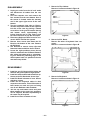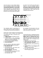
1
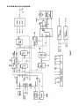
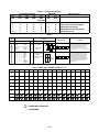
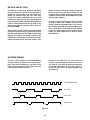
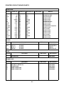
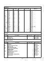
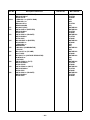
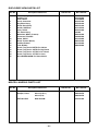
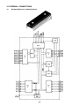
26-3011
TRS-80®
MICRO COLOR COMPUTER
MODEL MC-10
Catalog Number 26-3011
CUSTOM MANUFACTURED FOR RADIO SHACK, A DIVISION OF TANDY CORPORATION
TABLE OF CONTENTS
SECTION
NUMBER
PAGE
NUMBER
I
SYSTEM DESCRIPTION - - - - - - - - - - - - - - - - - - - - - - - - - - - - - - - - - - - - - - - - - - - - - 3
II
SPECIFICATIONS - - - - - - - - - - - - - - - - - - - - - - - - - - - - - - - - - - - - - - - - - - - - - - - - - - 7
III
DISASSEMBLY / REASSEMBLY - - - - - - - - - - - - - - - - - - - - - - - - - - - - - - - - - - - - - - - 9
IV
THEORY OF OPERATION - - - - - - - - - - - - - - - - - - - - - - - - - - - - - - - - - - - - - - - - - - CPU-6803 - - - - - - - - - - - - - - - - - - - - - - - - - - - - - - - - - - - - - - - - - - - - - - - - - - - - Reset Circuit - - - - - - - - - - - - - - - - - - - - - - - - - - - - - - - - - - - - - - - - - - - - - - - - - - ROM - - - - - - - - - - - - - - - - - - - - - - - - - - - - - - - - - - - - - - - - - - - - - - - - - - - - - - - - Cassette Interface - - - - - - - - - - - - - - - - - - - - - - - - - - - - - - - - - - - - - - - - - - - - - - Detailed Tape Format Information - - - - - - - - - - - - - - - - - - - - - - - - - - - - - - - - - - RS-232C Interface - - - - - - - - - - - - - - - - - - - - - - - - - - - - - - - - - - - - - - - - - - - - - - I/O Connector - - - - - - - - - - - - - - - - - - - - - - - - - - - - - - - - - - - - - - - - - - - - - - - - - Keyboard Interface - - - - - - - - - - - - - - - - - - - - - - - - - - - - - - - - - - - - - - - - - - - - - TV Switch Box - - - - - - - - - - - - - - - - - - - - - - - - - - - - - - - - - - - - - - - - - - - - - - - - Power Supply - - - - - - - - - - - - - - - - - - - - - - - - - - - - - - - - - - - - - - - - - - - - - - - - - VDG - - - - - - - - - - - - - - - - - - - - - - - - - - - - - - - - - - - - - - - - - - - - - - - - - - - - - - - - Device Selection - - - - - - - - - - - - - - - - - - - - - - - - - - - - - - - - - - - - - - - - - - - - - - - System Timing - - - - - - - - - - - - - - - - - - - - - - - - - - - - - - - - - - - - - - - - - - - - - - - - RAM - - - - - - - - - - - - - - - - - - - - - - - - - - - - - - - - - - - - - - - - - - - - - - - - - - - - - - - - Modulator - - - - - - - - - - - - - - - - - - - - - - - - - - - - - - - - - - - - - - - - - - - - - - - - - - - - -
V
TROUBLESHOOTING - - - - - - - - - - - - - - - - - - - - - - - - - - - - - - - - - - - - - - - - - - - - - - 21
VI
PARTS LIST - - - - - - - - - - - - - - - - - - - - - - - - - - - - - - - - - - - - - - - - - - - - - - - - - - - - - 25
11
12
12
12
12
13
14
15
16
16
17
17
19
19
20
20
VII PRINTED CIRCUIT BOARDS - - - - - - - - - - - - - - - - - - - - - - - - - - - - - - - - - - - - - - - - 30
VIII IC INTERNAL CONNECTIONS - - - - - - - - - - - - - - - - - - - - - - - - - - - - - - - - - - - - - - - 33
IX
SCHEMATlC DlAGRAM - - - - - - - - - - - - - - - - - - - - - - - - - - - - - - - - - - - - - - - - - - - - 44
X
EXPLODED VlEW - - - - - - - - - - - - - - - - - - - - - - - - - - - - - - - - - - - - - - - - - - - - - - - - - 46
[ Editor’s Note: I would also like to express my thanks to RadioShack for permitting the distribution of this manual. I hope you find it useful. I have found a few
typos and inconsistencies in the Service Manual that I have noted in an italized
font like this. JMM.]
–2–
SECTION I
SYSTEM DESCRIPTION
–3–
SYSTEM DESCRIPTION
The MC-10 Micro Color Computer is a fully
expandable microprocessor system. It is composed of a 6803 central processing unit, 4K of
static RAM, 8K of Basic ROM, and a 6847 video
display generator. The microcomputer is also
interfaced to a 48-key keyboard and provides
the logic to execute a 1500 Baud cassette interface and a RS-232 serial interface. The system
operates on a common color burst frequency
of 3.579545 MHz. This main clock is divided by
4 in the CPU to yield an operating speed of 0.89
MHz.
In operation, the 4K of static RAM is shared
between the CPU and the video display generator. This time multiplexing is based on the
processor clock E. The CPU will be granted
access to the RAM (upon request) only during
the high state of E. This allows efficient usage
of the RAM with no waiting by the CPU and no
visible conflict on the display.
The 6847 VDG provides a display on a TV
screen of 32 characters by 16 rows. It also
allows a 64 x 32 semigraphics mode with eight
colors. This display utilizes a minimum amount
of system RAM (512 bytes).
The final elements of the microcomputer system are the I/O devices. The MC-10 is interfaced
to a 48-key keyboard which generates the
codes for upper and lower case characters,
graphics symbols, and single stroke keyboard
entry. The computer also provides a 1500 baud
cassette interface for fast and reliable data and
program storage and a limited signal RS-232C
interface. The RS-232C interface allows either a
printer or a modem to be used with the MC-10.
–4–
SYSTEM BLOCK DIAGRAM
–5–
MEMORY MAP
Hex Address
C000 - FFFF
9000 - BFFF
4000 - 8FFF
0100 - 3FFF
0080 - 00FF
0015 - 007F
0014
0013
0012
0011
0010
000F
000E
000D
000C
000B
000A
0009
0008
0007
0006
0005
0004
0003
0002
0001
0000
16K ROM (only 8K used)
16K I/O Slot (Keyboard and VDG control)
16K RAM (4K - 20K used)
Not Used
RAM internal to the 6803
Not Used
RAM Control Register
Not Used
Not Used
Not Used
Not Used
Port 3 Control and Status Register
Input Capture Register (low byte)
Input Capture Register (high byte)
Output Compare Register (low byte)
Output Compare Register (high byte)
Counter (low byte)
Counter (high byte)
Timer Control and Status Register
Not Used
Not Used
Not Used
Not Used
Miscellaneous I/O Data Register
Keyboard Output Lines
Data Direction Register for miscellaneous I/O
Data Direction Register for keyboard lines
–6–
SECTION II
SPECIFICATIONS
–7–
SPECIFICATIONS
Power Supply
AC/AC adaptor
RF Modulator
For U.S.A./CANADA
Output Impedance
RF Output Terminal
RF Output Level
Input
Output
120V/60Hz
8.0V/1.5A 16W
Ch.
3
4
FC (MHz)
61.25 +/-0.25
67.65
Fsc (MHz)
4.5 +/-0.2
4.5
75 ohm
RCA jack
1.5 - 2.8 mV at 75 ohm
Central Processing Unit
6803 8-bit processor
clock speed 0.89 MHz
Memory Size
ROM (for BASIC)
RAM
Video Display
Character display
Semi-Graphic display
Color
8K
4K (expandable up to
20K-external)
512 (32 x 16) upper case
characters
64 x 32 elements
8 colors - Green, Yellow,
Blue, Red, Buff, Cyan, Magenta, Orange
Interface
Printer
Cassette
Bus line
RS232C, 4 pin DIN
5-pin DIN 1500 baud
34-pin Cartridge connector
Switch Box
Isolation
more than 60 dB
Dimensions
8-1/2" x 1-7/8” x 7”
Weight
1.75 Ibs (.7875 kilograms)
–8–
SECTION III
DISASSEMBLY / REASSEMBLY
–9–
DISASSEMBLY
1. Removal of Top Cabinet
Remove 4 screws as shown in Figure A.
1. Unplug the units from the AC wall outlet
and disconnect all cables from the rear
panel.
2. Turn the computer over and remove the
four screws from the case bottom. One of
the screws is located under the warranty
seal in the upper right corner of the case
bottom.
3. Turn the computer right side up. Disconnect the snap locks located on the right and
left side of the case by placing a slotted
screw driver in the groove between the top
and bottom cases, approximately 2.7
inches from the rear of case. Push in and
turn the screwdriver to pop the case apart.
4. Disconnect Keyboard cable from wire connector. NOTE: Pull flat wire upward.
5. Remove three screws that fasten the PC
Board to the bottom of the case. Remove
the PC Board.
6. Use tweezers to remove eleven clips that
fasten the bottom shield to the P.C. Board.
7. Locate the eight positions where the top
shield is soldered to the PC Board. Remove
this solder with solder wick or a desoldering tool. Bend the protruding edge of the
shield upward until it is parallel to the slot
and remove top shield.
Figure A
2. Removal of P.C. Board
Remove flat wires of keyboard from connector.
Remove 3 screws as shown in Figure B.
REASSEMBLY
1. Install the top PC Board shield. Solder the
shield to the ground plane at eight points.
2. Install the bottom shield with metal side up.
Secure to the PC Board with eleven clips.
3. Install PC Board in bottom of case. Secure
with three screws.
4. Install the two keyboard cables in their
respective connectors. This will be easier if
both hands are used and you are facing
rear of unit. Refasten cable restraints.
5. Join the top and bottom cases and push
them together at the snap lock positions.
This is a tight fit, therefore repositioning of
the cases may be required.
6. Install four screws in bottom of case.
Figure B
3. Removal of Keyboard
Remove 4 screws as shown in Figure C.
Figure C
– 10 –
SECTION IV
THEORY OF OPERATION
– 11 –
CPU-6803
RESET CIRCUIT
The main component of this microcomputer
system is the 6803 CPU. This is a 40-pin integrated circuit which provides the address,
data, and miscellaneous control signals. The
CPU receives the main clock frequency of
3.579545 MHz from the modulator assembly
and divides this by 4 to produce an operating
frequency of 0.89 MHz. This frequency is available as the processor clock E.
The reset circuit is composed of switch S1
diode D9, resistor R24, capacitor C8, and two
gates of IC U12. R24 and C8 form a simple time
constant so that during power up or whenever
the reset switch is pressed, the reset line will
stay low for a few milliseconds before returning
to the high state. The reset input to the 6803
does not provide hysteresis so the reset signal
must be buffered by U12 before being connected to the CPU. The final component of the
circuit is diode D9 which is provided to allow
for rapid cycling of the power switch.
This processor chip is designed to be used in a
minimum hardware configuration so, I/O lines
are provided directly from the CPU chip. In the
MC-10 computer these I/O lines are used to
address the keyboard and to support the cassette and RS232 interface.
ROM
The MC-10 uses a single 8K x 8 ROM to store
the BASIC operating language. This is located
in a 16K memory map segment between hex
C000 - FFFF. This device is connected directly
to the multiplexed address/data, however any
possible contention is avoided by enabling the
ROM only during the high cycle of the E clock.
The 6803 CPU is able to support several different modes of operation. For the MC-10 the CPU
is operating in mode 2. The CPU mode is
selected at power-up by the state of lines P20,
P21, and P22. P20 and P22 are connected by a
diode to Reset so that during power-up these
lines are low. P21 is connected to a pull-up
resistor so that during power-up it is high.
CASSETTE INTERFACE
Mode 2 operates with 128 bytes of internal
RAM, a full 16 line address bus and an 8 bit
data bus which is multiplexed with the lower
eight address lines. Due to the multiplexed
address and data bus, two external devices are
required. A 74LS373 is used to latch the
address lines. This occurs during the low portion of the E clock when the CPU is not accessing external devices. The latch signal (AS) is
provided by the CPU. The other external device
is a 74LS245. This bi-directional buffer is
required to isolate the RAM output lines, which
are providing data to the video display generator during the low portion of the E clock, away
from the CPU data bus. This buffer is controlled
by the device selection logic.
The cassette interface is composed of an output attenuator connected to a CPU output line
and an input zero crossing detector. Most of
the important cassette parameters are controlled by software. However, there is no cassette motor relay in the Micro Color Computer
and cassette recorder operation must be manual.
The cassette format chosen uses a sinewave of
2400 or 1200 Hertz to yield a Baud rate of approximately 1500 Baud. In this format, a 0 (or
logic low) is represented by one cycle of 1200
Hertz. A 1 (or logic high) is represented by one
cycle of 2400 Hertz. A sample of data is shown
in Figure 2. A typical program tape would consist of a leader of alternating 1’s and 0’s, followed by one or more blocks of data. A block of
data is composed of 0 to 255 bytes of data with
a checksum, sync byte, and the block length.
The output circuit utilizes a CPU output line to
produce a sinewave of 1200 or 2400 Baud. This
signal is then attenuated to approximately 1
volt and connected to the auxiliary input of the
cassette recorder.
– 12 –
tor equal to 1/2 volt. Since the other input is
biased at 1 volt, the comparator output is
switched to the high state. If the AC input from
the recorder is positive, diode D6 is turned off
and the input to the comparator will be at some
point greater than 1 volt, in which case, the
comparator output will be low.
The input circuit is a zero crossing detector.
R12 is a termination resistor for the cassette
output. Resistors R16 and R17 are used to bias
one input of the comparator at 1 volt. The other
input is also biased at 1 volt by R15 and the
series combination of R14 and R13. If the AC
input from the recorder goes negative, diode
D6 turns on and sets the input to the compara-
REFERENCE SQUARE WAVE
0
1
0
0
1
1
0
1
COMPUTER MEMORY DATA
4.6v
D/A OUTPUT
0v
1v
0v
INPUT TO TAPE
2.5v
OUTPUT FROM TAPE
0v
2.5v
5v
INPUT TO THE PIA
0v
0
1
0
0
1
1
0
1
DATA STORED
IN MEMORY
This is shown inverted to indicate possible phase inversion by the tape recorder.
Figure 2. Sample Data of Cassette Format
The comparator output is open-collector so
pullup resistor R19 is provided to generate a
TTL signal. R18 is used to prevent oscillation of
the comparator. The final portion of the cassette circuit is capacitor C7 which is used to
isolate noise from the cassette cable.
DETAILED TAPE FORMAT INFORMATION
The standard MC-10 tape is composed of the
following items:
1. A leader consisting of 128 bytes of hex 55
2. A Namefile block
3. A blank section of tape approximately
equal to 0.5 seconds in length; this allows
BASIC time to evaluate the Namefile.
4. A second leader of 128 bytes of Hex 55
5. One or more Data blocks
6. An End of File block
The End of File block is a standard block with a
length of 0 and the block type equal to FFH. The
Namefile block is a standard block with a
length of 15 bytes (0FH) and the block type
equals 00H. The 15 bytes of data provide information to BASIC and are employed as described below:
1. Eight bytes for the program name
2. One file type byte - 00H = BASIC, 01H =
Data, 02H = Machine Language
3. One ASCII flag byte - 00H = Binary, FFH =
ASCII
4. One Gap flag byte - 01H = Continuous, FFH
= Gaps
5. Two bytes for the start address of a
machine language program
6. Two bytes for the load address of a
machine language program
The block format for Data blocks, Namefile
Blocks, or an End of File block is as follows:
1. One leader byte - 55H
2. One sync byte - 3CH
3. One block type byte — 01H = Data, FFH =
End of File, 00H - Namefile
4. One block length byte - 00H to FFH
5. Data - 0 to 255 bytes
6. One checksum byte - the sum of all the data
plus block type and block length
7. One leader byte - 55H
– 13 –
RS-232C INTERFACE
thus if the input voltage is greater than 2.6
volts, the comparator is turned on. The comparator outputs are open-collector so pull-up
resistors R8 and R9 are required.
The RS-232C interface utilizes a 4-pin DIN connector (J2). This interface allows the computer
to have serial communication with printers,
modem, or other computers. The four signals
used by the interface are:
1. CD — a status input line
2. RS232lN — serial data input
3. GROUND — zero voltage reference
4. RS232OUT — serial data out
[I think there is a consistent error in the documentation of the pins here, specifically, CD and
RS232IN are reversed.]
1.
2.
3.
4.
The pin configuration for the DIN connector is
shown in Figure 3.
RS232lN — serial data input
CD — a status input line
GROUND — zero voltage reference
RS232OUT — serial data out
[And the diagram should look like:]
RS232 OUT
4 1
CD
3 2
RS232 IN
RS232 OUT
4 1
RS232 IN
3 2
CD
Figure 3. RS-232C Connector Pin-Out
In general, an RS232C signal uses negative
logic. Therefore, a voltage greater than +3 volts
is defined as a SPACE, or logical 0. A voltage
less than -3 volts is defined as a MARK, or logical 1. The range of -3 to +3 volts is undefined.
The RS-232C interface circuitry is shown on the
upper right corner of the schematic. The output
signal from the CPU output P20 is tied to a
741C op-amp (U16). This same output is also
used for the cassette output, so care must be
taken to ensure that a cassette output does not
appear as an RS-232 output. The op-amp is referenced at 1.4 volts by resistors R2 and R3.
This reference causes the op-amp to swing between the two power supply voltages (Vcc and
Vee) as the TTL input switches states. A 100
ohm resistor (R1) is included to provide a current limit on the output. The two input signals
(RS232lN and CD) utilize identical circuits and
share a common bias resistor network.
RS232IN (pin 4 of U15) is tied to CPU input P22
and CD (pin 6 of U15) is tied to CPU input P23.
The inputs from the external device are connected to the positive side of a diode. This
diode blocks the application of a negative voltage to the comparator (U15). When a positive
voltage is applied, the diode conducts and the
voltage is applied to the input. The comparators are referenced at two volts, by R5 and R6,
[and the text should read...]
“The two input signals
(RS232lN and CD) utilize identical circuits and
share a common bias resistor network. CD (pin 4
of U15) is tied to CPU input P22 and RS232IN (pin
6 of U15) is tied to CPU input P23.”]
– 14 –
I/O CONNECTOR
external memory modules or ROM software
modules. Table 1 provides a complete list of the
signals and a brief description of each.
In addition to serial interfaces, the MC-10 also
provides a full complement of CPU bus signals
that are accessible at the 34-pin cartridge connector. This allows expansion of the MC-10 with
Table 1. I/O Connector Signals
Pin
1
2
3
4
5
6
7
8
9
10
11
12
13
14
15
16
17
18
19
20
21
22
23
24
25
26
27
28
29
30
Signal Name
GND
GND
D0
D1
D2
D3
D4
D5
D6
D7
R/W
A0
A1
A2
A3
A4
A5
A6
A7
A8
A9
A10
A11
A12
A13
A14
A15
E
SEL
RESET
31
32
33
34
NMI
+5v
GND
GND
Description
Signal Ground
Signal Ground
CPU Data Bit 0
CPU Data Bit 1
CPU Data Bit 2
CPU Data Bit 3
CPU Data Bit 4
CPU Data Bit 5
CPU Data Bit 6
CPU Data Bit 7
CPU Read/Write Signal
CPU Address Bit 0
CPU Address Bit 1
CPU Address Bit 2
CPU Address Bit 3
CPU Address Bit 4
CPU Address Bit 5
CPU Address Bit 6
CPU Address Bit 7
CPU Address Bit 8
CPU Address Bit 9
CPU Address Bit 10
CPU Address Bit 11
CPU Address Bit 12
CPU Address Bit 13
CPU Address Bit 14
CPU Address Bit 15
Main CPU Clock (0.89 MHz)
Input to Disable Device Selection
Main Reset and Power-up Clear Signal to
the System
Non-Maskable Interrupt to the CPU
+5 volts (250 mA)
Signal Ground
Signal Ground
– 15 –
KEYBOARD INTERFACE
To read the keyboard, only one column is
enabled by writing a zero to one of the eight
CPU I/O lines that corresponds to that column,
and by writing ones to all the other lines. If a
key has been pressed in that column, one of
the input lines will be a zero and the key location will correspond to the bit that is low. By
scanning each column in the keyboard, all of
the keys may be checked.
The Keyboard interface for the MC-10 utilizes
the I/O lines of the 6803 CPU to reduce the logic
required to a single six input CMOS buffer and
seven pull-up resistors.
TV SWITCH BOX
From the computer, the signal is connected to a
balun in the switch box which matches the
modulator’s 75-ohm output impedance to a
TV’s 300 ohm antenna input impedance. This
signal is then connected to the switch. The
switch is specially designed to provide the
60dB of isolation required between the computer and the TV antenna.
The antenna switch box consists of a switch
and a balun, with connectors provided for
attachment to the computer, the TV antenna,
and the home TV. The switch box is connected
to the customer’s TV through the 300 ohm twin
lead output. The TV antenna is attached directly
to the switch box. The computer output is connected through a 75-ohm coaxial cable to the
phone plug input on the switch box. Figure 4
shows a schematic of the antenna switch box.
60dB
SWITCH
COMPUTER
INPUT
TWIN LEAD OUTPUT
TO THE TV
BALUN
ATTENNA INPUT
300 0hm
Figure 4. Antenna Switch Box Schematic
– 16 –
POWER SUPPLY
In the MC-10 the 4K of RAM is shared between
the CPU and video display generator. This is
accomplished by providing buffers between
the address lines (U5 and U6) the data line (U7),
and synchronizing the operation of the VDG to
the CPU.
The MC-10 power supply utilizes an external
power pack to supply 8 VAC at 1.5 amps. This
input AC voltage is connected through the
power switch to the bridge rectifier. The MC-10
operates primarily on +5 volts, so the negative
output of the bridge is grounded to provide a
larger current capability to the positive supply.
The output from the bridge is filtered by C1 and
C5 and is connected to the +5 volt regulator.
The regulator provides +5 volts at a maximum
of 1.5 amps to the digital circuitry.
Normally the three buffers are disabled so that
the VDG address is being supplied to the RAM
and the RAM data is supplied to the VDG. However, during a CPU access to the RAM, the
three buffers are enabled and the MS* line is
used to disable the address lines of the
MC6847. This provides the CPU address to the
RAM chips and allows a CPU read or write
cycle to occur.
A small amount of negative voltage is required
to the RS-232 output op-amp. This current is
supplied by the simple circuit composed of D2,
D3, C3, C4, and C32. This circuit operates by
using capacitor C3 for isolation from the primary bridge circuit. Then the negative voltage
is rectified by D2 and D3. The negative supply
voltage is then filtered by C4 and C32 before
being connected to U16. This is an unregulated
output. However, when coupled with the output
from the main bridges, it provides a larger differential voltage (that is the source of the positive op-amp voltage) with no detrimental effects
on the operation of the op-amp.
VDG
The video interface function in the MC-10 is
performed by the MC6847. This is a flexible
video display generator that will produce nine
colors (eight colors and black), an alphanumeric display mode, and several high resolution graphics modes.
In the MC-10 the VDG is interfaced to 4K of
static RAM and the mode control inputs are
controlled by a 74LS174 register. However, the
only modes of operation which are supported
by the machine are the alphanumeric mode and
the alpha semigraphic-4 mode. Table 4 lists all
of the alphanumeric characters which may be
displayed by the VDG along with the hex code
which will produce the character. Table 2 lists
the required control bit values to produce the
MC-10 display modes.
– 17 –
Table 2. VDG Control Register
Control Register Bits
D5
D4
D3
A*/G
GMD
GM1
D6
CSS
0
0
1
1
X
0
0
0
0
0
X
X
X
X
X
DMA Bits
D6
D7
INV
A*/S
D2
GM2
(INT*/EXT)
X
X
X
X
X
0
0
0
0
0
0
1
0
1
X
Mode Selected
0
0
0
0
1
Alphanumerical green
Alphanumerical inverted green
Alphanumerical orange
Alphanumerical inverted orange
Semigraphics Four
Table 3
VDG
PINS
CSS
INV
0
0
COLOR
TV SCREEN
VDG DATA BUS
Character Color
Background Border
Display Mode
0
1
Green
Black
Black
Green
Black
32 Characters
in columns
0
1
Orange
Black
Black
Orange
Black
16 Characters
in rows
x
Lx C2 C1 C0
0
x
x
x
1
0
0
0
1
0
0
1
1
0
1
0
1
0
1
1
1
1
0
0
1
1
0
1
1
1
1
0
1
1
1
1
Color
Black
Green
Yellow
Blue
Red
Buff
Cyan
Magenta
Orange
8 dots
12 dots
x
7
0
L3
L2
L1
L0
The ALPHANUMERIC INTERNAL mode
uses an internal character generator which
contains the following five dot by seven
dot characters @ A B C D E F G H I J K L
MNOPQRSTUVWXYZ[\]➡ ➟
SP ! ” # $ % & ‘ ( ) * + , - . / 0 1 2 3 4 5 6 7 8
9:;<=>?
IN
V
ASCII code
5
64 Display elements
in columns
Black
COMMENTS
Detail
The SEMIGRAPHICS FOUR mode uses
an internal “coarse graphics” generator
in which a rectangle (eight dots by twelve
dots) is divided into four equal parts. The
luminance of each part is determined by
a corresponding bit on the VDG data bus.
The color of illummated parts is determined
by three bits. It requires 512 bytes of
display memory.
1 C 2 C1 C 0 L 3 L 2 L 1 L 0
32 Display elements
in rows
one
element
Table 4. AVAILABLE CHARACTERS (00 - 7F)
0
1
2
3
4
5
6
7
8
9
A
B
C
D
E
F
0
-
-
-
-
-
-
-
-
-
-
-
-
-
-
-
-
1
-
-
-
-
-
-
-
-
-
-
-
-
-
-
-
-
2
SPACE
BAR
!
“
#
$
%
&
‘
(
)
*
+
,
-
.
/
3
0
1
2
3
4
5
6
7
8
9
:
;
<
=
>
?
4
@
A
B
C
D
E
F
G
H
I
J
K
L
M
N
O
5
P
Q
R
S
T
U
V
W
X
Y
Z
[
\
]
➡
➟
6
@
A
B
C
D
E
F
G
H
I
J
K
L
M
N
O
7
P
Q
R
S
T
U
V
W
X
Y
Z
[
\
]
➡
➟
= INVERTED CHARACTER
-
= UNDEFINED
– 18 –
DEVICE SELECTION
allows an external device to change the MC-10
memory map. Also, the disable signal for the
memory write is ORed with A12 to prevent a
complete overlap of the 4K of RAM into the 16K
memory map segment.
A 74LS155 is used along with four OR gates
and two inverters to provide device selection in
the MC-10. The 74LS155 uses A15 and A14 to
divide the memory map into four 16K segments. The bottom 16K segment is not used
externally to the CPU. The next 16K segment is
used for system RAM. The third 16K segment is
used to read the keyboard and to write to the
VDG control register. The final 16K is reserved
for system ROM.
From the output of the 74LS155 the IY1 output
is used to switch the tri-state controls for the
memory address and data buffers. The IY2 output is ORed with R/W and inverted R/W to provide a write pulse to the VDG control register
(U8) and a read enable for the keyboard input
buffer. The final output (IY3) is used to select
the ROM chip.
Both sections of the LS155 are used so that all
of the device selects may be gated with E, while
the CPU write signal for the RAMs is gated with
window* (U18 pin 6). The disable inputs to the
74LS155 are tied through an inverter to the cartridge connector and to a pull-up resistor. This
SYSTEM TIMING
The main clock frequency of 3.579545 MHz is
produced by the oscillator circuit in the modulator. This clock is buffered by one gate of U12
before being connected to the CPU and to the
clock synchronization circuitry.
Internal to the CPU chip, the main clock frequency is divided by 4 to produce the processor clock E. This clock is used to synchronize
all system operations to the CPU. Figure 5
shows the main clock and timing signals used
in the MC-10.
3.579545 MHz CLK
E CLOCK
AS U1-39
WIN U18-6
Figure 5
– 19 –
MODULATOR
The MC6847 (VDG) has access to the RAM during the low portion of the E clock. Also during
the low portion of E, the signal AS is used to
latch the address lines in the latch (U2). During
the high portion of E, all CPU address and data
lines are valid and any accesses to the RAM or
ROM occur during this time.
The outputs from the MC6847 are connected
directly to the modulator. The modulator unit is
built around the MC1372. This is a linear integrated circuit which is designed to interface to
the MC6847 and produce an RF output for connection to the TV. Figure 6 shows a block diagram of the MC1372 chip.
The signal window is used for two purposes.
The first usage is to gate the write signal. The
2K x 8 static RAM requires setup and hold time
on the address and data line, during a write
cycle. The address and data lines are both valid
for the high portion of the E clock. By gating
the write pulse with window, a safety margin is
created, so that the write pulse will never go
low while the address or data is changing.
The 3.579545 MHz crystal and associated components are connected between pins 1 and 2.
This provides the color burst frequency and the
main clock for the MC-10. The duty cycle input
is left unconnected to produce a 50% duty
cycle clock.
The other inputs to the MC1372 are the luminance input, øA, øB, and the color reference
voltage input. All of these inputs are connected
directly to the MC6847 chip.
The second usage of the signal window is for
synchronization of the VDG and the CPU. The
two devices must be synchronized to allow
both the CPU and the VDG to use the system
RAM with no conflict. This has been accomplished in the MC-10 by forcing the VDG to
latch data at the end of the low portion of the E
clock. To do this, low transition of the signal
HS* is only allowed to happen during the active
portion of the signal window. If HS* occurs during the window, the latching of data will occur
at the end of the low portion of the E clock.
The chroma modulator output is filtered by an
R-C network between pins 8 and 10 of the
MC1372. Also the 4.5 MHz frequency modulated
sound signal is AC coupled in at pin 10. The
sound input to the modulator is used to frequency modulate the 4.5 MHz oscillator composed of Q1 and the associated circuitry.
The channel selection for the modulator is performed by the tank circuit between pins 13 and
14 of the MC1372. This circuit allows the RF
output to be switched from channel 3 to 4 by an
external switch input.
RAM
The final RF output of the modulator is available at pin 12 of the MC1372. However, before
this signal is connected to the output jack, a
vestigial sideband filter must be used to suppress unwanted harmonics of the signal. This
filter is shown in the schematic as the thirteen
passive components before the RF output.
The MC-10 uses two 2K x 8 static RAM chips for
a total internal memory of 4K. The RAM chips
receive their address lines from either the
MC6847 (VDG) or the CPU. This switching is
accomplished by tri-state buffers which are
controlled by the MS* line. The individual RAM
chip is selected by VA11, the 12th address line,
and since the OE* input is grounded, one RAM
is always enabled. The WE* line is generated by
the CPU address decoding logic, and is high
except when the CPU is writing to RAM.
COLOR B LUMINANCE
INPUT
INPUT
V CC
11
OSCILLATOR 2
INPUT
5
LAG
CHROMINANCE
OSCILLATOR
and
CLOCK
DRIVER
CLOCK
OUTPUT 1
LAG
4
3
GROUND DUTY CYCLE
ADJUST
9
CHROMA
MODULATOR
B
12
RF
MODULATOR
CHROMA
MODULATOR
A
7
RF
MODULATOR
OUTPUT
RF
OSCILLATOR
6
13
14
COLOR A COLOR
INPUT
REFERENCE RF TANK
INPUT
Figure 6. MC1372 Block Diagram
– 20 –
10
CHROMINANCE
INPUT
8
CHROMA
MODULATOR
OUTPUT
SECTION V
TROUBLESHOOTING
– 21 –
TROUBLESHOOTING
VIDEO INTERFACE
Problems with the MC-10 may be separated into
two major areas - I/O problems and dead computer problems. If the computer will display the
sign-on message, then a fairly simple set of
testing procedures may be used to isolate the
problem. If, however, the computer displays
random characters on the screen or has no display, then a major failure has occurred.
Almost all of the work for the video interface is
performed by the VDG (U11 - MC6847). Therefore, this chip is the most likely source of a
video problem. However, it is always a good
idea to isolate the source of a problem before
trying to desolder chips.
If the problem is no picture or a distorted picture, then a new switch box and cable should
be tried. If you still do not have a picture, then
use an oscilloscope to look at U11 pin 28. You
should have a video signal at this point. If you
do not have a video signal, check +5 volts (pin
17) and the 3.579 MHz clock (pin 33) , if you
have both of these inputs and no video out,
then U11 is bad.
In the case of a major failure, the first thing to
check is the +5-volt power supply. If the voltage
level is off by more than 10%, then the power
supply is the problem. Refer to the Power Supply section for hints on how to isolate the problem.
If the power supply has a proper +5 volts output, then check the clock output from the modulator at U12 pin 13. If the clock is oscillating at
the proper frequency, and you have no display,
the problem is in the video area. Refer to the
section on the video interface for hints on fixing this problem.
If you have a video signal at pin 28, but no picture on your TV, then there could be a problem
with the modulator. Check the +5-volt input
before replacing the modulator.
The only other type of video failure which can
occur in the MC-10 is the loss of synchronization with the CPU which will cause excess
glitches on the screen. If this occurs, then the
circuitry composed of U18 and U19 is failing.
If the MC-10 displays garbage on the screen,
then some problem is causing a failure of the
CPU. At this point you will have to remove the
top and bottom shield. After you have removed
the two shields, test the operation of the MC-10
to be sure that the problem was not a short to
the shield.
KEYBOARD INTERFACE
With both of the shields removed, check the
address and data lines of the 6803. After the
reset switch has been pressed, check for indications that the CPU is operating. If the CPU
shows no signs of activity, then one of the
input signals is preventing the CPU from operating or the CPU is bad.
The keyboard interface is composed of one
resistor pack and one IC (U14). A keyboard failure will usually be caused by a mechanical failure of the keyboard, or a short or open in the
cable. Mechanical failures will usually be only
one or two isolated keys failing. Cable failures
will cause an entire keyboard row or column to
fail.
If the CPU is operating, then the most likely
problems are a memory or buffer chip failure or
a short on the address or data bus. In this case
you will have to methodically check the
address and data lines, while looking for a line
that shows a problem.
In the case of a simple I/O problem, please refer
to the appropriate interface section discussion.
– 22 –
RS-232 INTERFACE
ground. If this shows zero resistance, the problem is a short to ground.
The RS-232 interface uses three simple level
converter circuits. Isolating the problem will be
an easy job of comparing the input to the output.
If the +5 output is not shorted, check the voltage with the power pack plugged in. You
should have 8 VAC at the power ON-OFF
switch. If this looks good, check the input to
the regulator. Here you should see a full wave
rectified voltage of 10 volts DC. If you do not,
one of the following components could be bad:
D1; CI [C1] or C5; U15, U16, or U17.
Connect a DIN-type plug to the serial I/O jack to
short together pins 1, 2, and 4. Now, type in the
following test program:
5 POKE 3,1
10 FOR X=0 TO 10: NEXT X
15 POKE3,0
20 FOR X=0 TO 10: NEXT X
25 GOTO 5
The only major remaining component is the +5volt regulator. If the regutator is receiving the
proper input voltage, and there is no +5 volts,
the regulator chip is bad.
Run the program and check pin 2 of U16; a
switching TTL waveform should be present. Pin
6 of U16 should have the same waveform
except that it will be switching from +Vcc to
-Vcc (the supply voltages of pins 4 and 7 of
U16). Also check pins 4 and 6 of U15. These
pins have the same waveform switching from 0
to +Vcc. The outputs of U15, pins 1 and 2
should show the original TTL signal.
Also, there is a simple circuit to supply an
unregulated negative voltage to the RS-232
interface. If you are missing the negative voltage but the +5 volts is OK, then one of the
diodes or the capacitors has failed.
CASSETTE INTERFACE
If clock does not appear at TP 2, there could be
a problem with the modulator.
MODULATOR
If you are having problems with the cassette
circuit, short together pins 4 and 5 of the cassette DIN plug. Next run the program listed for
the RS-232 interface test. The output pin is
shared between RS-232 and cassette, so this
test program will produce a switching TTL
waveform on the output.
Check the +5 volts (pin 11 of MC1372) and the
3.579 MHz clock (pin 1 of MC1372).
If you cannot see the 3.579 MHz clock, check
parts connected to pin 1 and pin 2 (R1, C2, C3,
X1) .
If the 3.579 MHz clock is OK but picture is distorted, try to tune TV set by adjusting fine tuning.
The output circuit is a simple attenuator, so the
likely failure here should be a short to ground.
The output on pin 5 of the DIN connector
should be switching for 0 to +1 volt.
If picture is distorted even after fine turning
adjustment, replace modulator unit if you do
not have Spectrum Analyzer.
The input circuit is a zero crossing detector. It
should convert the cassette signal back to the
original TTL waveform at pin 13 of U15.
If you have a spectrum analyzer, you can adjust
inside of modulator.
Remove the modulator first.
POWER SUPPLY
Refer to disassembly instruction on page 10
and locate the four positions where modulator
is soldered to P.C. Board. Remove this solder
with solder wick or desoldering tool.
The power supply circuit in the MC-10 has a
minimum component count so that a failure
should be readily identifiable.
Bend the protruding edge of modulator until it
is parallel to the slot and remove modulator.
The first place to check if the computer has no
+5-volt supply voltage is the output of the regulator. With the power pack unplugged, measure
the resistance between the +5 output and
– 23 –
ADJUSTMENT OF VSB (vestigial side band)
FILTER
CH. 4
Make Connection according to Figure 7
IC1
Luminance In
12
RF Out
RCA
JACK
0.01
5 ± 0.1V
C116
L102 L103
L101
75Ω Coaxial
Cable
DC Power
Supply
SPECTRUM
ANALYZER
75Ω COAXIAL
CABLE
INPUT
TRACKING
GENERATOR
2.
3.
4.
5.
6.
7.
50/75Ω Impedance
Video Carrier
Figure 7
Adjust marker of tracking generator at
61.25 MHz (marker - 2)
Adjust L102 so lower side band peak point
meets 61.25 MHz (marker - 2)
Adjust marker of tracking generator at
72.15 MHz (marker - 3)
Adjust L103 so higher side peak point
meets 72.15 MHz (marker - 3)
Repeat steps 1 to 4 until lower and higher
side band peaks agree with 61.25 MHz
(marker - 2) and 72.15 MHz (marker - 3)
Refer to Figure 8
Adjust L101 so that filter characteristic of -1
dB stays about within 12 MHz.
Adjust marker point of tracking generator
at 57 MHz (marker - 1) and check the level
difference between 61.25 MHz (lower side
peak point - marker 2) and 57 MHz (marker 1) is more than 20 dB.
Sound Carrier
Freq. (MHz)
4.5
2
4.5
ADJUSTMENT OF SOUND CARRIER
FREQUENCY
T101
IC1
R103
Q1
10
470 pF
Sound
In
Frequency
Counter
Figure 10
Prepare capacitor of 470 µF [pF] and make connection according to Figure 10.
Adjust T101 core so that freq. counter shows
4.500 MHz.
12 MHz
2 dB
50/75Ω
Impedance
Figure 9
SPECTRUM
ANALYZER
OUT
1.
CH. 3
0.01
MDV - 1
Sound In
RF OUT
C117
CH. Select
3
20 dB
1 dB
1
ADJUSTMENT OF CHROMATIC FREQUENCY
Freq.
57
61.25
72.15
(MHz)
Make connection according to Figure 11.
Figure 8
ADJUSTMENT
QUENCY
OF
VIDEO
CARRIER
Adjust trimmer capacitor C102 so that freq.
counter shows 3.579545 MHz.
FRE-
Prepare switch, 0.01 µF capacitor and 2.2K ohm
resistor and 75 ohm coaxial cable with RCA
and 50/75 ohm converter.
5 ± 0.1V
MDV-1
CLK
OUT
Regulated
D.C. Power
Supply
Make connection according to Figure 9.
1. Set switch to CH 4.
2. Adjust T102 core so that frequency counter
of spectrum analyzer shows 67.65 MHz
3. Set switch to CH 3.
4. Adjust trimmer capacitor of C113 so that
frequency counter of spectrum analyzer
shows 61.25 MHz.
0.001
Freq.
Counter
Figure 11
Note: On actual board, unit of hundred of the
reference numbers is omitted. Ex. L102 is
marked “L2.”
– 24 –
SECTION VI
PARTS LIST
– 25 –
PRINTED CIRCUIT BOARD PARTS
CAPACITORS
Ref.No.
Value (µF)
C1
C2
C3/4
C5
C6
C7
C8
C9~12
C13
C14~20
C21/22
C23
C24~26
C27
C28
C29
C30~32
C33
4700
10
100
0.1
0.0022
0.022
4.7
0.022
0.1
0.1
0.022
0.022
0.022
0.1
0.022
0.022
0.022
150P
Voltage (V)
Tolerance ( %)
16
25
16
25
50
50
50
50
25
50
50
16
50
25
50
16
50
50
±20
±20
±20
±20
+80/-20
+80/-20
±20
+80/-20
±20
±5
+80/-20
±30
±80/-20
±20
+80/-20
±30
+80/-20
±5
R/S Part No.
Material
Radial Electrolytic
Radial Electrolytic
Axial Electrolytic
Radial Ceramic
Radial Ceramic
Radial Ceramic
Radial Electrolytic
Radial Ceramic
Radial Ceramic
Radial M-Plastic Capacitor
Radial Ceramic
Axial Ceramic
Radial Ceramic
Radial Ceramic
Radial Ceramic
Axial Ceramic
Radial Ceramic
Radial Ceramic
DIODES
Ref. No.
D1
D2/3
D4~9
Description
SIRBA10
10E1 or
SR1K-2
1N4148
R/S Part No.
RECTIFIER
SI DIODE
SI DIODE
SI DIODE
Manufacture
SHINDENGEN
NIHONINTER or
UNIZON
HITACHI or ITT
CORE
Ref. No.
FB1~5
Description
R/S Part No.
CORE φ3.5 x φ1.3 x 5 or
BL01RN1-A61
Mfr’s Part No.
588010050A
588010060A
CONNECTORS
Ref. No.
J1
J2
J3
J4
J5
Description
R/S Part No.
5P DIN (For CASSETTE I/O)
4P DIN (For SERIAL I/O)
POWER JACK
WIRE CONNECTOR
WIRE CONNECTOR
Mfr’s Part No.
193410030A
193410020A
196610020A
193904400A
193904400A
– 26 –
RESISTORS
Ref.No.
Value (ohms)
R1
R2
R3
R4
R5
R6/7
R8/9
R10
R11
R12
R13
R14
R15/16
R17
R18
R19
R20
R21
R22/23
R24
R25
R26
100
3.9K
1.5K
10K
15K
10K
4.7K
75K
24K
220
8.2K
6.8K
56K
15K
1.5M
4.7K
10K x 8
4.7K
4.7K
100K
4.7K
100K
Wattage
1/2
1/6
1/6
1/4
1/4
1/4
1/4
1/6
1/6
1/4
1/4
1/4
1/4
1/4
1/4
1/4
1/4
1/4
1/6
1/4
1/4
1/4
Tolerance ( %)
±5
±5
±5
±5
±5
±5
±5
±5
±5
±5
±5
±5
±5
±5
±5
±5
±5
±5
±5
±5
±5
±5
R/S Part No.
Material
Carbon
Carbon
Carbon
Carbon
Carbon
Carbon
Carbon
Carbon
Carbon
Carbon
Carbon
Carbon
Carbon
Carbon
Carbon
Carbon
Resistor Array
Carbon
Carbon
Carbon
Carbon
Carbon
SWITCHES
Ref. No.
S1
S2
S3
Description
R/S Part No.
RESET SW
POWER SW
CHANNEL SW
Mfr’s Part No.
187010040A
183110240A
183110280A
INTEGRATED CIRCUITS
Ref. No.
U1
U2
U3
U4
U5/6
U7
Description
R/S Part No.
MC6803G or (MCU)
HD6803P
SN74LS373N or (D-LATCH)
MB74LS373M
MB8364M (MASK ROM)
SN74LS155N or (DECODER)
MB74LS155M or
HD74LS155P
SN74LS367AN or (DRIVER)
MB74LS367AM or
HD74LS367AP
SN74LS245N or (TRANSCEIVER)
MB74LS245M
Mfr’s Part No.
MOTOROLA
HITACHI
MOTOROLA
FUJITSU
FUJITSU
MOTOROLA
FUJITSU
HITACHI
MOTOROLA
FUJITSU
HITACHI
MOTOROLA
FUJITSU
– 27 –
Ref. No.
U8
U9/10
U11
U12
U13
U14
U15
U16
U17
U18
U19
U20
Description R/S Part No.
SN74LS174N or (D-TYPE F.F)
MB74LS174M or
HD74LS174P
µPD4016C-1 or (STATIC RAM)
µPD4016D-1 or
MB8128-15P or
MSM2128-20RS
MC6847P (VDG)
SN74LS14N or (INVERTER)
MB74LS14M or
HD74LS14P
SN74LS32N or (OR-GATE)
MB74LS32M or
HD74LS32P
MC14503BCP or (BUFFER)
HD14503BP or
µPD4503BC or
MSM4503RS
LM339N or (COMPARATOR)
µPC339C
MC1741CP1 or (OP AMP)
HA17741PS
MC7805CT or (VOLTAGE REGULATOR)
NJM7805A or
µPC7805H
SN74LS74AN or (D-F.F)
MB74LS74AM or
HD74LS74AP
SN74LS76AN or (JK-F.F)
MB74LS76AM or
HD74LS76P
SN74LS32N or (OR-GATE)
MB74LS32M or
HD74LS32P
– 28 –
R/S Part No.
Mfr’s Part No.
MOTOROLA
FUJITSU
HITACHI
NEC
NEC
FUJITSU
OKI
MOTOROLA
MOTOROLA
FUJITSU
HITACHI
MOTOROLA
FUJITSU
HITACHI
MOTOROLA
HITACHI
NEC
OKI
MOTOROLA
NEC
MOTOROLA
HITACHI
MOTOROLA
JRC
NEC
MOTOROLA
FUJITSU
HITACHI
MOTOROLA
FUJITSU
HITACHI
MOTOROLA
FUJITSU
HITACHI
EXPLODED VIEW PARTS LIST
Ref. No.
1
2
3
4
5
6
7
8
9
10
11
12
13
F1
F2
F3
F4
F5
Description R/S Part No.
R/S Part No.
Cabinet Ass’y, Top
Cabinet, Top
Plate, Model
Cover, Connector
Key Board Ass’y
Knob, Reset (Red)
Holder, SW Reset
Case, Shield
P.C. Board Ass’y
Modulator, MDV-1 (Custom)
Connector, Flat Wire
Sheet, Shield
Knob, Channel (Black)
Cabinet, Bottom
Foot, Rubber
Screw, Top Tite 3x12 BT-B For Cabinet
Screw, Top Tite 3x 8 BT-B For Key Board
Screw, Top Tite 3x 8 PT-B For P.C. Board
Screw, Top Tite 3x 6 PT-B For Cover
Rivet HARRA002SW For Sheet, Shield
Mfr’s Part No.
M00324
601210420A
711010040A
851210720A
187510010A
659510310A
411101870A
473010160A
U32008
525010030A
193903430A
473310380A
659510320A
601310290A
608010080A
MISCELLANEOUS PARTS LIST
Ref. No.
Description R/S Part No.
PATCH CORD
Mfr’s Part No.
189510020A
Box, Switch
Adaptor, Power
R/S Part No.
AC-AC (U.S.A.)
10901008TA
AC-AC (CA)
10901009TA
RCA-RCA 2M
313510100A
– 29 –
SECTION VII
PRINTED CIRCUIT BOARDS
– 30 –
MAIN P.C.B.
(TOP VIEW)
– 31 –
(BOTTOM VIEW)
– 32 –
SECTION VIII
IC INTERNAL CONNECTIONS
– 33 –
IC INTERNAL CONNECTIONS
U1
MC6803G (Motorola) or HD6803P (Hitachi)
– 34 –
U11
MC6847P (Motorola)
– 35 –
U2
SN74LS373N (Motorola) or MB74LS373M (Fujitsu)
U7
SN74LS245N (Motorola) or MB74LS245M (Fujitsu)
– 36 –
U3
MB8364M (Fujitsu)
U9/10 µPD4016C-1 (NEC) or µPD4016D-1 (NEC) or MB8128-15P (Fujitsu) or MSM2128-20RS (Oki)
– 37 –
U4
SN74LS155N (Motorola) or MB74LS155M (Fujitsu) or HD74LS155P (Hitachi)
U5/6
SN74LS367AN (Motorola) or MB74LS367AM (Fujitsu) or HD74LS367AP (Hitachi)
– 38 –
U8
SN74LS174N (Motorola) or MB74LS174M (Fujitsu) or HD74LS174P (Hitachi)
U14
MC14503BCP (Motorola) or HD14503BP (Hitachi) or µPD4503BC (NEC) or MSM4503RS (Oki)
U19
SN74LS76AN (Motorola) or MB74LS76AM (Fujitsu) or HD74LS76P (Hitachi)
– 39 –
U12
SN74LS14N (Motorola) or MB74LS14M (Fujitsu) or HD74LS14P (Hitachi)
U13
SN74LS32N (Motorola) or MB74LS32M (Fujitsu) or HD74LS32P (Hitachi)
U20
SN74LS32N (Motorola) or MB74LS32M (Fujitsu) or HD74LS32P (Hitachi)
– 40 –
U15
LM339N (Motorola) or µPC339C (NEC)
U18
SN74LS74AN (Motorola) or MB74LS74AM (Fujitsu) or HD74LS74AP (Hitachi)
– 41 –
U16
MC1741CP1 (Motorola) or HA17741PS (Hitachi)
U17
MC7805CT (Motorola) or NJM7805A (JRC) or µPC7805H (NEC)
– 42 –
SECTION IX
SCHEMATlC DlAGRAM
SECTION X
EXPLODED VlEW
– 43 –
RADIO SHACK, A DIVISION OF TANDY CORPORATION
U.S.A.: FORT WORTH, TEXAS 76102
CANADA: BARRIE. ONTARIO L4M 4W5
TANDY CORPORATION
6A3
AUSTRALIA
BELGIUM
U. K.
91 KURRAJONG ROAD
PARC INDUSTRIEL DE NANINNE
BILSTON ROAD WEONESBURY
MOUNT ORUITT, N.S.W. 2770
5140 NANINNE
WEST MIDLANDS WS10 7JN
Printed in U.S.A.