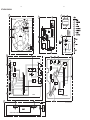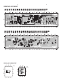
1
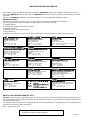
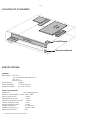
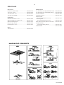
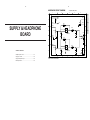
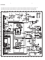
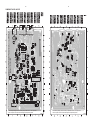
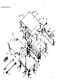
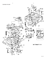
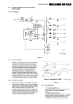
CC3000 /N1B, /U1B, /K1B, /N2B, /U2B, /K2B
CC4000 /U1B, /K1B, /F1B, /U2B, /K2B, /F2B
CC4000F /U1B, /K1B, /U2B, /K2B
5Disc CD Changer
COMPACT
DIGITAL AUDIO
TABLE OF CONTENTS
Variation Table .............................................................................................................. 1-1
Location of pc boards & Technical Specifications ........................................................ 1-2
Service Aids, Chip Handling ........................................................................................ 1-3
ESD, Safety Instruction, etc. ......................................................................................... 1-4
Disassembly Instructions & Service positions .............................................................. 3-1
Service Test Programs ................................................................................................. 3-3
Set Block diagram ............................................................................................................ 4
Set Wiring diagram ........................................................................................................... 5
Supply & Headphone Boards ........................................................................................... 6
Front Board ...................................................................................................................... 7
Servo/Decoder Board ...................................................................................................... 8
DAC/AF Board .................................................................................................................. 9
Mechanical Exploded views & parts list ......................................................................... 10
Please use this service manual with referring to the user guide (D.F.U) without fail.
R
- CC3000 / CC4000 / CC4000OSE 278W855010 ACT
3120 785 22010
First Issue:1999.08
CC3000/4000
Service
Manual
MARANTZ DESIGN AND SERVICE
Using superior design and selected high grade components, MARANTZ company has created the ultimate in stereo sound.
Only original MARANTZ parts can insure that your MARANTZ product will continue to perform to the specifications for which
it is famous.
Parts for your MARANTZ equipment are generally available to our National Marantz Subsidiary or Agent.
ORDERING PARTS :
Parts can be ordered either by mail or by Fax.. In both cases, the correct part number has to be specified.
The following information must be supplied to eliminate delays in processing your order :
1. Complete address
2. Complete part numbers and quantities required
3. Description of parts
4. Model number for which part is required
5. Way of shipment
6. Signature : any order form or Fax. must be signed, otherwise such part order will be considered as null and void.
USA
EUROPE / TRADING
MARANTZ EUROPE B.V.
P.O.BOX 80002, BUILDING SFF2
5600 JB EINDHOVEN
THE NETHERLANDS
PHONE : +31 - 40 - 2732241
FAX
: +31 - 40 - 2735578
MARANTZ AMERICA, INC.
INC
440 MEDINAH ROAD
ROSELLE, ILLINOIS 60172
USA
PHONE : 630 - 307 - 3100
FAX
: 630 - 307 - 2687
AMERICAS
SUPERSCOPE TECHNOLOGIES, INC.
MARANTZ PROFESSIONAL PRODUCTS
2640 WHITE OAK CIRCLE, SUITE A
AURORA, ILLINOIS 60504 USA
PHONE : 630 - 820 - 4800
FAX
: 630 - 820 - 8103
AUSTRALIA
JAMO AUSTRALIA PTY LTD
1 EXPO COURT, P.O. BOX 350
MT. WAVERLEY VIC 3149
AUSTRALIA
PHONE : +61 - 3 - 9543 - 1522
FAX
: +61 - 3 - 9543 - 3677
BRAZIL
MARANTZ BRAZIL
CAIXA POSTAL 21462
CEP 04698-970
SAO PAULO, SP, BRAZIL
PHONE : 0800 - 123123(Discagem Direta Gratuita)
FAX
: +55 11 534. 8988
CANADA
LENBROOK INDUSTRIES LIMITED
633 GRANITE COURT,
PICKERING, ONTARIO L1W 3K1
CANADA
PHONE : 905 - 831 - 6333
FAX
: 905 - 831 - 6936
THAILAND
MRZ STANDARD CO.,LTD
746 - 754 MAHACHAI ROAD.,
WANGBURAPAPIROM, PHRANAKORN,
BANGKOK, 10200 THAILAND
PHONE : +66 - 2 - 222 9181
FAX
: +66 - 2 - 224 6795
TAIWAN
PAI- YUING CO., LTD.
6 TH FL NO, 148 SUNG KIANG ROAD,
TAIPEI, 10429, TAIWAN R.O.C.
PHONE : +886 - 2 - 25221304
FAX
: +886 - 2 - 25630415
JAPAN Technical
MARANTZ JAPAN, INC.
35- 1, 7- CHOME, SAGAMIONO
SAGAMIHARA - SHI, KANAGAWA
JAPAN 228-8505
PHONE : +81 42 748 1013
FAX
: +81 42 748 9190
SINGAPORE
WO KEE HONG (S) PTE LTD
WO KEE HONG CENTRE
NO.23, LORONG 8, TOA PAYOH
SINGAPORE 319257
PHONE : +65 2544555
FAX
: +65 2502213
MALAYSIA
WO KEE HONG ELECTRONICS SDN. BHD.
NO. 102 JALAN SS 21/35, DAMANSARA
UTAMA, 47400 PETALING JAYA
SELANGOR DARUL EHSAN, MALAYSIA
PHONE : +60 3 - 7184666
FAX
: +60 3 - 7173828
KOREA
MK ENTERPRISES LTD.
ROOM 604/605, ELECTRO-OFFICETEL, 16-58,
3GA, HANGANG-RO, YONGSAN-KU, SEOUL
KOREA
PHONE : +822 - 3232 - 155
FAX
: +822 - 3232 - 154
SHOCK, FIRE HAZARD SERVICE TEST :
CAUTION : After servicing this appliance and prior to returning to customer, measure the resistance between either primary AC
cord connector pins ( with unit NOT connected to AC mains and its Power switch ON ), and the face or Front Panel of product and
controls and chassis bottom.
Any resistance measurement less than 1 Megohms should cause unit to be repaired or corrected before AC power is applied, and
verified before it is return to the user/customer.
Ref. UL Standard No. 1492.
In case of difficulties, do not hesitate to contact the Technical
Department at above mentioned address.
990805ACT
1-1
VARIATION TABLE
Type:
CC4000
CC4000F
-
X
(CC4000OSE)
X
CC-DAC(Non-bitstream)
X
-
-
TDA1545AT/N2
BCC-DAC(Bitstream)
-
X
X
NJM4560D
NJM2114D
NJM2114D
Features:
Headphone
TDA1549T/N1
OP-AMP
for LPF
Mains Transformer Type
CC3000
EI-48
EI-54
EI-54
(Except /K)
-
-
*1
for DAC/AF BOARD
Special ELE.CAP.
-
-
*2
for SUPPLY BOARD
Additional Bottom Plate
-
-
X
Remote Control (RC4000CC)
X
X
X
RC5 In/Out
X
X
X
Digital Out (COAX)
X
X
X
CD Text
-
-
-
CDRW(Play Rewritable Disc)
X
X
X
Special ELE.CAP.
*1
(1) Item2895/2896 Elcap R20 50V S 10uF PM20 A (2020 012 93203)
(2) Item2897 Elcap ROA 50V S 47uF PM20 A (2020 012 93432)
(3) Item2899 Elcap ARS 25V S 47uF PM20 A (4822 124 12023)
(4) Item2902 Elcap ARS 25V S 47uF PM20 A (4822 124 12023)
(5) Item2905/2906 Elcap S 47uF 6V3 BIP (ELNA) A (4822 124 80954)
*2
Item2510 Elcap R20 16V S 2200uF PM20 (4822 124 40723)
1-2
DEC SE
OD RVO
ER /
BO
ARD
DAC
BO / AF
ARD
SUP
PLY
BO
AR
D
LOCATION OF PC BOARDS
H/P BO
ARD
FRON
T BOA
RD
Load/QP Board
Open/close Board
SPECIFICATIONS
GENERAL:
Mains voltage : 100V for /F
110-127V/220-240V Switchable for /K
120V for /U
220-230V for /N
Mains frequency
Power consumption
: 50/60Hz
: < 12W at Play mode
Dimension (WxDxH)
: 435 x 380 x 119mm
AUDIO PERFORMANCE:
Output level
: 2Vrms ± 2dB @ 47kohm
Frequency response within ± 0.4dB : 20Hz - 20kHz
Dynamic range at 1kHz
: > 90dB 1)
Signal/Noise ratio at 1kHz
Total Harmonic Distortion at 1kHz
: > 98dB 1)
: < 0.004%
Channel unbalance at 1kHz
Channel separation at 1kHz
: < 1dB
: > 95dB 1)
Headphone impedance
Headphone output (e.m.f.)
: 30 - 600 ohm
: 4.5Vrms ± 2dB
Digital Output at 75ohm
: 0.5V
1)
with 13th order Filter eg. 4822 395 30204
1-3
SERVICE AIDS
Service Tools:
ESD Equipment:
Universal Torx driver holder .................................. 4822 395 91019
Anti-static table mat - large 1200x650x1.25mm ... 4822 466 10953
Torx bit T10 150mm ............................................. 4822 395 50456
Anti-static table mat - small 600x650x1.25mm ..... 4822 466 10958
Torx driver set T6 - T20 ......................................... 4822 395 50145
Anti-static wristband .............................................. 4822 395 10223
Torx driver T10 extended ...................................... 4822 395 50423
Connector box (1MΩ) ............................................ 4822 320 11307
Extension cable
Compact Disc:
SBC426/426A Test disc 5 + 5A ............................ 4822 397 30096
(to connect wristband to conn. box) .................. 4822 320 11305
Connecting cable
SBC442 Audio Burn-in Test disc 1kHz ................. 4822 397 30155
(to connect table mat to conn. box) .................. 4822 320 11306
SBC429 Audio Signals disc .................................. 4822 397 30184
Earth cable (to connect product to mat or box) .... 4822 320 11308
Dolby Pro-logic Test Disc ...................................... 4822 395 10216
Complete kit ESD3
Eccentricity Disc, 150µm ....................................... 4822 397 30279
(combining all above products) ......................... 4822 320 10671
Wristband tester .................................................... 4822 344 13999
Others:
13th Order Filter .................................................... 4822 395 30204
HANDLING CHIP COMPONENTS
PCS 101 006
1-4
GB
NL
ESD
WARNING
Alle IC’s en vele andere halfgeleiders zijn
gevoelig voor electrostatische ontladingen
(ESD).
Onzorgvuldig behandelen tijdens reparatie kan
de levensduur drastisch doen verminderen.
Zorg ervoor dat u tijdens reparatie via een
polsband met weerstand verbonden bent met
hetzelfde potentiaal als de massa van het
apparaat.
Houd componenten en hulpmiddelen ook op
ditzelfde potentiaal.
All ICs and many other semi-conductors are
susceptible to electrostatic discharges (ESD).
Careless handling during repair can reduce life
drastically.
When repairing, make sure that you are
connected with the same potential as the mass
of the set via a wrist wrap with resistance.
Keep components and tools also at this
potential.
F
WAARSCHUWING
ATTENTION
I
Tous les IC et beaucoup d’autres
semi-conducteurs sont sensibles aux
décharges statiques (ESD).
Leur longévité pourrait être considérablement
écourtée par le fait qu’aucune précaution n’est
prise à leur manipulation.
Lors de réparations, s’assurer de bien être relié
au même potentiel que la masse de l’appareil et
enfiler le bracelet serti d’une résistance de
sécurité.
Veiller à ce que les composants ainsi que les
outils que l’on utilise soient également à ce
potentiel.
D
AVVERTIMENTO
WARNUNG
Alle ICs und viele andere Halbleiter sind
empfindlich gegenüber elektrostatischen
Entladungen (ESD).
Unsorgfältige Behandlung im Reparaturfall kan
die Lebensdauer drastisch reduzieren.
Veranlassen Sie, dass Sie im Reparaturfall über
ein Pulsarmband mit Widerstand verbunden
sind mit dem gleichen Potential wie die Masse
des Gerätes.
Bauteile und Hilfsmittel auch auf dieses gleiche
Potential halten.
Tutti IC e parecchi semi-conduttori sono
sensibili alle scariche statiche (ESD).
La loro longevità potrebbe essere fortemente
ridatta in caso di non osservazione della più
grande cauzione alla loro manipolazione.
Durante le riparazioni occorre quindi essere
collegato allo stesso potenziale che quello della
massa dell’apparecchio tramite un braccialetto
a resistenza.
Assicurarsi che i componenti e anche gli utensili
con quali si lavora siano anche a questo
potenziale.
GB
Safety regulations require that the set be restored to its original
condition and that parts which are identical with those specified,
be used.
“Pour votre sécurité, ces documents
doivent être utilisés par des spécialistes agréés, seuls habilités à réparer
votre appareil en panne”.
NL
Veiligheidsbepalingen vereisen, dat het apparaat bij reparatie in
zijn oorspronkelijke toestand wordt teruggebracht en dat onderdelen,
identiek aan de gespecificeerde, worden toegepast.
CLASS 1
LASER PRODUCT
3122 110 03420
F
Les normes de sécurité exigent que l’appareil soit remis à l’état
d’origine et que soient utiliséés les piéces de rechange identiques
à celles spécifiées.
GB
Warning !
Invisible laser radiation when open.
Avoid direct exposure to beam.
D
Bei jeder Reparatur sind die geltenden Sicherheitsvorschriften zu
beachten. Der Original zustand des Geräts darf nicht verändert werden;
für Reparaturen sind Original-Ersatzteile zu verwenden.
S
Varning !
Osynlig laserstrålning när apparaten är öppnad och spärren
är urkopplad. Betrakta ej strålen.
SF Varoitus !
I
Le norme di sicurezza esigono che l’apparecchio venga rimesso
nelle condizioni originali e che siano utilizzati i pezzi di ricambio
identici a quelli specificati.
Avatussa laitteessa ja suojalukituksen ohitettaessa olet alttiina
näkymättömälle laserisäteilylle. Älä katso säteeseen!
DK Advarse !
"After servicing and before returning set to customer perform a
leakage current measurement test from all exposed metal parts to
earth ground to assure no shock hazard exist. The leakage current
must not exceed 0.5mA."
PCS 101 007
Usynlig laserstråling ved åbning når sikkerhedsafbrydere er
ude af funktion. Undgå udsaettelse for stråling.
3-1
3-1
DISMANTLING INSTRUCTIONS
Dismantling of the DAC/AF board, Supply board and Front Panel Assembly
Dismantling of the Tray Assembly and Servo board
1) Remove the Top Cover (pos 151) by 8 screws.
- 2 screws on each side
1) Remove the Metal rod (pos 152) as indicated.
2) Loosen the Crank CDC5 (pos 96) with screw D and lift the
- 4 screws from the rear
2) Remove the DAC/AF board by 5 screws A. Be careful not
4) Turn the crank CDC5 (pos 96) clockwise to slide out the
tray assembly.
Tray moves out
crank arm out of the groove on the tray assembly. The
complete tray assembly can be pulled out of the Frame
Dismantling of the CD Mechanism
1) Loosen the Pressure ring holder (pos 90) by relasing catch
C3 as indicated.
2) Remove the Pressure plate (pos 89) and Rotary disc
assembly (pos 100) by 1 screw F.
(pos93).
to damage flex cable.
Turn
5) With the set upside-down, release the 2 catches C1 and
remove the tray cover as indicated.
6) Loosen the Front Panel assembly from the bottom bracket
(pos 181) by 5 screws C and 4 catches C2 as indicated.
3) Remove the Supply board by 3 screws B and disconnect
the Lever Power button (pos 6) as indicated.
- 2 screws on top
- 3 screws from the bottom side
3) Turn the Tray assembly upside-down and remove the
CDM Lock (pos 99) by using a "minus" screw-driver to
3) Remove the Servo board by 2 screws E.
release 2 catches C4 as indicated.
4) Protect the CD mechanism's Laser against ESD by shortcircuiting the flexfoil with a paper clip immediately upon
disconnection from the flexfoil connector.
(See Warning for more details)
4) With the Tray assembly facing up again, turn the cam
wheel (pos 116) to bring the CD mechanism (pos 98) to the
down position. Remove the CD mechanism by sliding out
the 4 rubber suspension (pos 104 to 107).
PCS 101 015
3-2
Assembly of the CD mechanism and Rotary disc CDC5
1) Remove the 4 rubber suspension (pos 104-107) from the
Support bracket (pos 114) and attached them on to the
CD mechanism.
2) Place the CD mechanism with the rubber suspension
above the mounting 4 holes.
3) Hold the CD mechanism in position and pull the tips of the
rubber suspension through the holes in the Support
bracket.
3-2
Warning
Charged capacitors on the Servo board may damage the
CD drive electronics when connecting a new CD mechanism. That's why, besides the safety measures like
* Switch off power supply
* ESD protection
Additional actions must be taken by the repair technician.
SERVICE POSITION 1
The following steps have to be done when replacing the CD
Mechanism:
1) Disconnect the old CD mechanism flexfoil from printed
board.
2) Connect paperclip to CD mechanism flexfoil to shortcircuit flexfoil (fig.1).
3) Short-circuit printed board with brass-sheet (4822 321
11197) plugged into the flexfoil connector (fig. 2).
4) Remove the old CD mechanism.
5) Assemble the new CD mechanism into position.
5) Remove short-circuit from printed board connector.
6) Remove short-circuit from flexfoil of new CD mechanism.
7) Connect new flexfoil to print connector (fig. 3).
4) After assembly of the CD Mechanism, the Cam wheel (pos
116) and the Rotary disc (pos 100) must be re-aligned.
This is done by positioning the Bearing (pos 101), pin on
the Cam wheel and CD Mechanism in a straight line as
indicated.
5) Assemble the Rotary disc onto the Bearing with the "1"
Figure 1
SERVICE POSITION 2
printing mark facing the CD Mechanism.
Figure 2
Figure 3
PCS 101 016
3-3
SERVICE TEST PROGRAM I
3-3
To start service test program
hold STOP & PLAY
depressed while
plugging in the mains cord
S refers to Service Mode.
Display shows the
ROM version *
"S V yy"
(Main menu)
V refers to Version.
yy refers to Software version number of ∝Processor.
(Counting up from 01 to 99)
MAIN MENU
DISPLAY
TEST
QUARTZ
TEST
TIME
Button pressed?
N
PROGRAM
Button pressed?
Y
N
SHUFFLE
Button pressed?
TIME
Button pressed?
Display shows
8M
Output at (Front Board)
pin 80 of uP = 1,953.125Hz
N
PLAY
Button pressed?
Y
Any Button
pressed?
N
N
NEXT Button
pressed?
Y
FOR CD Test
see page 3-4
Display shows "--"
N
STOP
Button pressed?
N
SERVICE
PLAY MODE
Y
Y
Display shows
Figure 1
CD
TEST
KEY TEST
Set is in Service PLAY Mode.
This mode is intended for
- CD PLAY Test
The CD PLAY is intended to
detect intermittent or not reproducible failures.
This is done by continuously playing a disc.
N
In case of failures, error codes according
to table 2 will be displayed.
Y
Y
Y
Display according
to Table 1
Display shows
Figure 2
STOP
Button pressed?
STOP
Button pressed?
N
Y
TRACK
4
3
PEAK
TOT
REM
TRACK
TIME
5
2
PROGRAM
1
FTS
TRACK
SHUFFLE
TOT
CD
+G
TRACK
REPEAT
E1000
W
E1001
W
E1002
W
Sledge In Error
The sledge did not reach its inner position (inner-switch is still close) before approximately 6 Sec. have
passed by. Inner-switch or sledge motor problem.
E1003
W
Sledge Out Error
The sledge did not come out of its inner position (inner-switch is still open) before approximately 250 mSec.
have passed by. Inner-switch or sledge motor problem.
E1005
W
Jump error
Triggered in normal play when the jump destination could not be found within a certain time.
Focus Error
Triggered when the focus lost for a certain time during play.
Radial Error
Triggered when the radial servo is not on track for a certain time during play.
Keys
activated
Display
shows
Keys
activated
Display
shows
Keys
activated
Display
shows
E1006
W
Subcode Error
Triggered when a no valid subcode for a certain time during play.
No Key pressed
--
Pause
7
Disc 3
15
E1007
W
PLL Error
The Phase Lock Loop could not lock within a certain time.
Any Remote control key
RC
Previous
8
Disc 4
16
Program
1
Turntable Motor Error
Generated when the CD could not reached 75% of speed during startup within a certain time. Discmotor problem.
9
Disc 5
17
E1008
W
Next
Scan
2
Stop
Exit
Open/Close
18
E1020
F
Focus Search Error
The focus point has not been found within a certain time.
Repeat
3
Play
11
Quick Play
19
Edit
4
Shuffle
12
Load
20
E1070
W
Time
5
Disc 1
13
E1071
W
Fader
6
Disc 2
14
The carousel position switch did not close within a certain time. This can happen when the switch is defective
and never closes electrically, or when the carousel is blocked in between two disc positions. The time-out is
approximately 5 Sec.
E1079
W
The drawer could not enter the inside position and is opening again. This can be caused because the drawer is
blocked by something and cannot go fully inside, or the drawer switch is defective and does not close.
SHUFFLE VIDEO CD -I+G PAUSE REPEAT 1 DISC
Figure 1
Type
N
Y
Error Description
Error code
The carousel switch is not open within certain time. This can happen when either the switch is defective and
closed all the time, or when the carousel is blocked in between two disc positions.
The time-out is approximately 5 seconds.
DISC
Figure 2
F = Fatal error & the set stop play function
Table 1
W = Warning
Table 2
PCS 101 017
3-4
SERVICE TEST PROGRAM II
3-4
To start service test program
hold STOP & PLAY
depressed while
plugging in the mains cord
Display shows the
ROM version
"S V yy"
(Main menu)
S
refers to Service Mode.
V
refers to Version.
yy refers to Software version
number of ∝Processor.
(Counting up from 01 to 99)
N
NEXT
Button pressed?
Y
Display shows
"CD"
CD Menu
Changer
Mechanism
Test
Tray Motor
Test
Tray
Motor Test
Sledge
Motor Test
Disc
Motor Test
Changer
Mech. Test
N N
PLAY
Button pressed?
OPEN/CLOSE
Button pressed?
STOP
Button pressed?
N
N
CD_X #
Button pressed?
Y
Y
Y
Y
Change to
selected disc
Is FOCUS found?
Is tray
closed?
N
Y
Focus Servo Test
Y
Open Tray
Tray
Motor Test
N
Sledge
Motor Test
Disc
Motor Test
Changer
Mech. Test
Display shows
Display shows
"FOC OK"
"FOC ERR"
PLAY
Button pressed?
STOP
Button pressed?
Y
Y
N
Sledge
Motor Test
N
Y
Disc Servo Test
Display becomes
Display remains as
"DISC OK"
"DISC ERR"
Radial Servo Test
Disc Motor
Test
NEXT
Button pressed?
N
PLAY
Button pressed?
Close Tray
Sledge Motor
Test
"DISC"
Y
# CD_X refers to CD1, CD2 or CD3
N
Display shows
Disc starts turning,
is speed ok?
N
N
PREVIOUS
Button pressed?
SHUFFLE
Button pressed?
Y
Y
"RDL"
NEXT
Button pressed?
Y
N
PREVIOUS
Button pressed?
Jump tracks Test
STOP
Button pressed?
Y
Y
Sledge jumps outward in
steps of 16-tracks
PCS 101 018
Sledge jumps inward in
steps of 16-tracks
Y
Sledge moves inside
Display shows
Disc Motor turns Counter
Clockwise & Display shows
Disc Motor turns
Clockwise & Display shows
"SLD I"
"CCW"
"CW"
STOP
Button pressed?
1) If the Tray Motor test is done with the Tray in the open position, the tray
will close only after the pressing the Open/Close button twice.
N
PROGRAM
Button pressed?
"SLD 0"
Note: In software version 15 and below there are some slight problems in the
Service Program for the CD Test which will be resolved by running change.
The problems are:
Display shows
N
Sledge moves outside
Display shows
Y
Y
N
2) If this test is performed after the Tray Motor Test, the tray may not change
as selected. The test will resumed correctly if CD test is quit and restarted.
3) After performing the Sledge Motor Test or Disc Motor Test the set will
return automatically to the "CD Menu".
4-1
4-1
SET BLOCK DIAGRAM
FTD
µP
CC4000
CC4000F
only
5-1
5-1
SET WIRING DIAGRAM
L
T
P
TRAY LOADER
TRANSFORMER
H
POWER SUPPLY
HP PANEL
CC4000 / CC4000F only
D
S
DAC/AF
SERVO/DECODER
C
3139 119 30820 dd wk 852
CONTROL & DISPLAY PANEL
6-1
6-1
HEADPHONE CIRCUIT DIAGRAM
1
+10V
2
1370 - 2
3
4
5
6
1370
1370
1370
1370
1370
1371
1372
A
1372
2380
2381
2382
2383
3380
3380
3381
3382
3383
3384
B 3385
3386
3999
7380
7380
+10V
1372 - 1
2380
22n
A
-10V
VHP R
1370 - 1
-10V
1372 - 2
2383
3384
15k
100n
1370 - 3
3386
3380
GND
1370 - 4
120R
1
3
10k
B
2
10k
SUPPLY & HEADPHONE
BOARD
CC4000/CC4000F ONLY
2381
10n
7380
NJM4556 (A)
3382
2
R
3383
15k
C
1371
L
3
C
+10V
1
VHP L
8
1370 - 5
3385
6
4
D
10k
TABLE OF CONTENTS
120R
5
10k
3380
7
3381
2382
10n
7380
NJM4556 (B)
-10V
Headphone part - Circuit ................................................. 6-1
Supply part - Circuit ......................................................... 6-2
Supply & Heaphone layout .............................................. 6-2
Electrical parts list ............................................................ 6-3
1
2
CONN. 1370 TO CONN. 1301 ON DAC CIRCUIT
3
3999*
D
* For Testing only
4
5
6
3086_0283_2
A1
A1
B1
C1
C1
B6
A6
A6
A1
B5
D5
A6
B1
D1
D3
B3
C3
A3
D4
B4
D6
B4
D4
6-2
6-2
POWER SUPPLY CIRCUIT DIAGRAM
HEADPHONE & SUPPLY BOARD LAYOUT
10
22n
6504
2
3
1N4003G
1
6505
BZX79C3V9
-3.9V
5
1005 - 5
VFTD
-27V
1
1543
2508
220u
50V
1542-1
2509
22u
50V
C
1005 - 4
4
1542-2
GND
1
1503 - 6
8.6V
1540 - 2
1501
MAINS
1503 - 5
0V
3n3 400V
1500
9505
9503
2501
22n
1542-5
0V
6501
1N4003G
1503 - 4
8.6V
1541-3
6507
1N4003G
6508
1N4003G
6502
1N4003G
6503
1N4003G
2502
22n
+10V
1005 1
2503
22n
1502
F
G
1
-10
2
E
2510
2200uF
16V
VERSION VARIATIONS
XXX
/K
/N
1501
T80mA
1502
T100mA
1541
x
1542
x
1543
x
9501
9502
x
9503
x
9504
x
9505
x
9506
x
x - Item in used
D
-10V
2
1005
9506
E
+10
2506
6800u
16V
-
2544
D
6500
1N4003G
-
2500
22n
+3.9V
/U, /F
T200mA
x
x
x
-
6560
3560
1k
1
1005 - 3
1N4003G
6561
2560
6562
1N4003G
330u 16V
BZX79C3V9
2
KILL
F
1
3380
6
L
R
3
9000
22-40
3460
9
4
A
7460
1005
1
1501
B
9506
9502
9001
2560
B
6562
6560
3560
9501
6561
6508
6507
1
2510
1541
2544
C
2501
6501
6500
2500
2506
2503
6503
1542
1
6502
2502
2504
6504
C
1543
2505
6506
3
1
4
6505
2507
2
2508
2509
1503
5
1
D
D
1502
2507
100n
G
This assembly drawing shows a summary of all possible versions. For components
used in a specific version see schematic diagram and respective parts list.
Date: wk853.1
2
4.6803
A
2382
B
6506
BZV85-C7V5
2381
C B E
7500
28V
2
22n
-36V
3385 3386
3383
7380
2383
1372
2460
1503 - 3
7500
MC7924
2505
1
240V T80mA
230V T80mA
117V T200mA
3
C
VAC1
3382
3999
-
2504
1542-4
B
9504
1005 - 6
1541-2
4.6803 311 4013
1408
1370
9
4
9502
CC4000 / CC4000F only
1540
-19.5V
4.8V
1503 1
1540 - 1
MAINS
VAC2
22-40
1541-1
1005 - 7
3
1
-
1503 2
1542-3
2
1
A
1
9505
A
9501
1005 D10
1005 E10
1005 F10
1005 C10
1005 B10
1005 B10
1005 A10
1500 D 2
1501 D 1
1502 E 2
1503 B 6
1503 A 6
1503 B 6
1503 E 6
1503 D 6
1503 D 6
1540 B 1
1540 D 1
1541 A 3
1541 B 3
1541 E 3
1542 A 3
1542 B 3
1542 C 3
1542 C 3
1542 D 3
1543 C 2
2500 D 7
2501 D 7
2502 D 9
2503 D 9
2504 B 6
2505 B 7
2506 D 9
2507 G 9
2508 C 8
2509 C 9
2510 E 7
2544 D 2
2560 F 9
3560 F 9
6500 D 7
6501 D 7
6502 D 8
6503 D 8
6504 B 7
6505 C 9
6506 B 9
6507 D 8
6508 D 8
6560 F 8
6561 F 8
6562 F 9
7500 B 8
9501 A 2
9502 B 2
9503 D 3
9504 C 2
9505 D 2
9506 E 1
CONN.1005 TO CONN.1008
ON DECODER CIRCUIT
5500 (Mains Transformer)
GND
9
9504
8
3384
7
1371
6
9503
5
3381
4
2380
3
4.6803 311 4013
2
1500
1
3
4
5
6
7
8
9
1
10
2
1005
1370
1371
1372
1408
1500
1501
1502
1503
1540
1541
1542
1543
2380
2381
2382
2383
2460
2500
2501
2502
2503
2504
2505
2506
2507
2508
2509
2510
2544
2560
3380
3381
3382
3383
3384
3385
3386
3460
3560
3999
6500
6501
6502
6503
6504
6505
6506
6507
6508
6560
6561
6562
7380
7460
7500
9000
9001
3
TRANSFORMER CONNECTIONS
RED
240V
/F VERSION
RED
RED
ACF1
ACF1
BLACK
240V
RED
ACF1
ACF1
BLACK
BLUE
BLUE
117V
RED
220V-230V
/K VERSION
/U VERSION
/N VERSION
BLUE
BLUE
RED
220V-230V
ACF2
ACF2
BLUE
BLUE
BLUE
WHITE
BLUE
RED
BROWN
BLUE RED
RED
ORANGE BLUE BLACK
127V
BLUE
RED BROWN
ORANGE
RED
110V
WHITE
BLUE
WHITE
AC1
AC1
VFTD
VFTD
BLUE
BLACK
ACF2
BLUE
RED
BROWN
RED
BLUE RED
RED
GREEN
0V
GND
0V
GREEN
GND
130 oC
WHITE GREEN WHITE
0V
GND
THERMAL FUSE
NOT SERVICEABLE
WHITE GREEN WHITE
BROWN
GREEN
GND
THERMAL FUSE
NOT SERVICEABLE
0V
AC2
AC2
GREEN
BROWN
WHITE
WHITE
RED
AC1
130 oC
THERMAL FUSE
NOT SERVICEABLE
BROWN
THERMAL FUSE
NOT SERVICEABLE
BROWN
BROWN
WHITE
AC1
130 oC
130 oC
RED
ACF2
BLUE
VFTD
VFTD
100V
RED
WHITE
WHITE
AC2
AC2
WHITE GREEN WHITE
WHITE GREEN WHITE
A
A
A
A
A
B
B
C
D
B
B
C
D
A
A
A
A
A
C
C
C
C
C
C
C
D
D
D
C
C
B
A
A
A
A
A
A
A
A
B
A
C
C
C
C
C
D
D
B
B
B
B
B
A
A
C
A
B
3
1
2
1
3
1
2
2
3
2
1
1
1
1
2
2
1
3
3
3
3
3
3
3
3
3
3
3
3
1
3
1
1
2
1
1
1
2
2
3
2
3
3
3
3
3
3
3
3
3
3
3
3
1
2
3
1
3
9501
9502
9503
9504
9505
9506
B
B
C
C
C
B
1
2
1
2
2
2
6-3
ELECTRICAL PARTS LIST - SUPPLY & HEADPHONE BOARD
MISCELLANEOUS
1371 482 2267 31453
1500 482 2276 13224
1501 482 2252 51167
1501 482 2071 58009
1501 482 2071 52001
1502 482 2070 31001
1540 482 2265 20723
1543 482 2277 11237
Headphone Socket
for CC4000, CC4000F
!
!
!
!
!
!
!
Power Switch
FUSE T200mA 250V for /U
FUSE T80mA 250V for /N
FUSE T200mA 250V for /F
FUSE T100mA 250V for /K
Socket. Primary Winding
Voltage Selector for /K
2380 482 2126 11585
22nF+80-20% 25V
for CC4000, CC4000F
2381 482 2121 51387
2382 482 2121 51387
10nF20% 16V for CC4000, CC4000F
10nF20% 16V for CC4000, CC4000F
2383 482 2126 12882
100nF+80-20% 50V
for CC4000, CC4000F
2500 482 2126 11585
2501 482 2126 11585
22nF+80-20% 25V
22nF+80-20% 25V
2502 482 2126 11585
2503 482 2126 11585
22nF+80-20% 25V
22nF+80-20% 25V
2504 482 2126 11585
2505 482 2126 11585
22nF+80-20% 25V
22nF+80-20% 25V
2506 482 2124 12328
2507 482 2126 12882
6800µF 16V
100nF+80-20% 50V
2508 482 2124 11769
2509 482 2124 81151
220µF 20% 50V
22µF 50V
2510 482 2123 14025
2510 482 2124 40723
2200U 20% 16V for CC4000
2200µF 20% 16V
2560 482 2124 40849
1N4003G
6504 482 2130 31878
6505 482 2130 31981
1N4003G
BZX79-B3V9
6506 532 2130 32586
6507 482 2130 31878
BZV85-C7V5
1N4003G
6508 482 2130 31878
6560 482 2130 31878
1N4003G
1N4003G
6561 482 2130 31878
6562 482 2130 31981
1N4003G
BZX79-B3V9
TRANSISTORS & INTEGRATED CIRCUITS
CAPACITORS
2544 482 2126 14504
6503 482 2130 31878
!
for CC3000, CC4000F
3.3nF 20% 250V
330µF 20% 16V
RESISTORS
3380 482 2101 21199
10kX2 20%
3381 482 2116 83864
for CC4000, CC4000F
10k 5% 0.5W for CC4000, CC4000F
3382 482 2116 83864
3383 482 2116 52244
10k 5% 0.5W for CC4000, CC4000F
15k 5% 0.5W for CC4000, CC4000F
3384 482 2116 52244
3385 482 2116 52206
15k 5% 0.5W for CC4000, CC4000F
120R 5% 0.5W for CC4000, CC4000F
3386 482 2116 52206
3560 482 2050 11002
120R 5% 0.5W for CC4000, CC4000F
1k 1% 0.4W
3999 482 2116 52303
3999 482 2116 52297
8k2 5% 0.5W for /U, /F
68k 5% 0.5W for /N
3999 482 2116 52228
680R 5% 0.5W for /K
DIODES
6500 482 2130 31878
6501 482 2130 31878
1N4003G
1N4003G
6502 482 2130 31878
1N4003G
7380 482 2209 82362
7500 482 2209 31257
NJM4556D for CC4000, CC4000F
MC79L24ACP
Note: Only the parts mentioned in this list are normal
service spare parts.
7-1
7-1
LCD DISPLAY PIN CONNECTIONS
6G
7G
TRACK
4
4G
3G
PEAK
TOT
REM
2G
TRACK
1G
TIME
5
3
FRONT BOARD
5G
2
PROGRAM
1
FTS
SHUFFLE VIDEO CD -I+G PAUSE REPEAT 1 DISC
8G
a
k
f
j
b
g
g
p
e
c
n
d
( 6G - 1G )
TABLE OF CONTENTS
LCD Pin connections ....................................................... 7-1
Circuit diagram - Main part .............................................. 7-2
Component & Chip layouts - Main part ........................... 7-3
Circuit diagram & layout - Open/Close part .................... 7-3
Electrical parts list ............................................................ 7-4
1G
2G
3G
4G
5G
6G
7G
8G
P1
TIME
TRACK
REM
TOT
PEAK
TRACK
1
SHUFFLE
P2
a
a
a
a
a
a
2
VIDEO
P3
b
b
b
b
b
b
3
CD
P4
f
f
f
f
f
f
4
-I
P5
j
j
j
j
j
j
5
+G
P6
k
k
Dp
-
Col
-
P7
g
g
g
g
g
g
PROGRAM
REPEAT
P8
c
c
c
c
c
c
FTS
1
P9
e
e
e
e
e
e
-
DISC
P10
p
p
p
p
p
p
-
-
P11
n
n
n
n
n
n
-
-
P12
d
d
d
d
d
d
-
-
PAUSE
PCS 101 024
7-2
7-2
CIRCUIT DIAGRAM - MAIN PART
42 D14
1400 A5
1403 D1
1404 G1
1405 F1
1407 C11
1408 D11
1409 C12
1410 D10
1411 D11
1412 C11
1414 E10
1415 E11
1416 E11
1417 F11
1418 E12
1
1419 C13
1420 E12
1421 C12
1422 D12
2401 C2
2402 D2
2403 D3
2404 G1
1423 D12
1424 F12
1425 F12
1427 C10
2
2405 F6
2406 F6
2407 G6
2408 G7
2409 G7
2410 G7
2411 G8
2412 G8
3
2413 C9
2414 C10
2415 D10
2416 E10
2421 E4
2422 E4
2423 E4
3401 C2
2417 F10
2418 F1
2419 D4
2420 D4
4
3402 C2
3405 F8
3406 F8
3407 G9
3408 G9
3409 G7
3410 G7
3411 G7
5
3412 F8
3413 F6
3414 F6
3415 F6
3416 F5
3417 F5
3418 F5
3419 F5
6
1400
8-BT-213GK
3420 F5
3421 E3
3422 E4
3423 E3
7
FTS SHUFFLE PAUSE SCAN
TITLE CHAPTER
TRACK
A-B
3428 D9
3429 E9
3430 E9
3431 E9
3424 E4
3425 E3
3426 D4
3427 C9
3432 E9
3433 B10
3434 C11
3435 C11
3436 C12
3437 C10
3438 D11
3439 D11
8
3440 D12
3441 E10
3442 E11
3443 E11
3448 F11
3449 F11
3450 F12
3451 F12
3444 E12
3445 E12
3446 C13
3447 F10
9
3452 D13
3453 G3
3454 D12
3455 C12
10
11
1 2
7409 H9
7410 F9
7411 F7
9480 C9
12
13
14
12 13 14 15 +
4 5 6 7 8 92
110 11 12 13 14 15 16 17 18 19
0
22 23 24 25 26 27 29 30
P12
P11
P10
P09
P08
P07
P06
P05
P04
P03
P02
P01
G01
G02
G03
G04
G05
G06
G07
G08
F1
B
B
3435
3436
3455
3446
820R
1K2
2K2
4K7
D_GND
22K
3R3
3426 1K
PROGRAM
COUNTER
P42
69
35 P61
P43
70
P44
71
P45
72
P46
73
P47
74
P50
75
P51
76
P52
77
P53
78
26 P01
P54
79
25 P00
P55
80
34 P60
CPU
VDD
32 P07
1421
1412
1407
2414
220p
1427
3439
3440
3454
3452
1
680R
820R
1K2
2K2
4K7
2
D
3K9
DIPMATE
1K2
2K2
4K7
3432
1K
7408
2404
1420
1416
1415
1414
2416
220p
E
+5V
3449
3450
3451
820R
1K2
2K2
1417
2417
220p
T
F
1425
3448
680R
1424
3K9
3447
3462
150R
+5V
7410
BC857B
3460
KILL2
RC5BusOut
1418
3459
820R
T
+5V
47R
3407
2n2
2411
100n
3408
10K
G
2
VSUPPLY
47n
2412
3
3K9
3445
680R
3406
1K
100K
CdSicl
100n
2
2408
2407
CdSild
47K
BC847B
10n
3409
1K
1
3441
3444
KeySet4
6401
P10
1
3443
3431
BZX79-F3V3
P11
2
3442
1K
1K
P12
3
KeySet3
3461
P13
4
KeySet2
1K
22K
I/O PORT 5
P14
5
1K
1K
P15
6
3429
1K
3405
P16
7
3412
P17
8
9 TEST
10 P21
11 P22
12 RESET
13 XIN
14 XOUT
15 VSS
1K
3430
3410
3411
2409
RC5Bus
CdPore
cdTxtClk
cdTxtIn
CdSicl
CdSild
CdData
4K7
CdData
D_GND
KeySet1
+5V
100n
1404
22K
3453
EH-B
3428
3463
2410
cdTxtClk
+5V
16 P20
17 P30
BC857B
7411
22n
4
I/O PORT 1
2406
33p
2418
3
6 BIT A/DCONVERTER
CST
5400
33p
2405
cdTxD
3414 1K
cdTxtIn
2
1K 3413
1405
1
I/O PORT 3
cdTxD
7401
TMP87CN71
18 P31
100n
10n
2423
100n
2422
2421
1K
19 P32
1K
3416 1K
CdCarSw
3421
3415 1K
CdCarSw
3422
8 BIT
TIMER/COUNTER
(I/O PORT 2)
20 P33
CdTraySw
12
CdTraySw
1K
27 P02
21 P34
11
1K
INTERRUPT
CONTROLLER
CLOCK/TIMING CONTROLLER
330R
CdSledgeSw
3423
28 P03
3417 1K
CdSledgeSw
29 P04
3424
22 P35
CdTrayCtrl
10
100R
1K
3418
3425
I/O PORT 0
CdTrayCtrl
16 BIT
TIMER/COUNTER
23 P36
CdDisPosSw
9
30 P05
24 P37
8
CdDisDetect
CdDisPosSw
31 P06
3465
3419 470R
CdDisDetect
3420 470R
CdCarCtrl
4
CdPore
42
3438
T
220p
I/O PORT 6
PROGR MEMORY
(ROM)
48KX8 BIT
100n
1423
68
+5V
6
7
CdCarCtrl
F
DATA MEMORY
(RAM)
1024X8 BIT
I/O PORT 4
1u
36 P62
33 VDD
3464
5
2420
5401 2u2
3466
4
1u
2419
100u
2403
47K
47K
47K
-Vkk
-VFTD
+5B
3458
3
3457
3456
2
VAC2
37 P63
F2
1u
1403 EH-B
1
VAC1
2402
4R7
38 P64
+5V
1422
67
P41
VKK
3402
1408
P40
C
+5V
2413
1411
66
3437
65
1410
P97
VKK
9480
64
P96
3427
63
P95
I/O PORT 9
I/O PORT 8
39 P65
1R
62
P94
60
P92
61
59
P91
P93
58
52
P82
P90
51
P81
57
50
P80
56
49
P77
P87
48
P76
P86
47
P75
55
46
P74
P85
45
54
44
P72
P73
P84
43
53
42
P71
I/O PORT 7
P83
41
P70
40 P66
2415
F1
1u
4R7
2401
3401
C
P67
T
1419
3434
680R
1409
3K9
3433
P12
P11
P09
P10
P08
P07
P06
P05
P04
P03
P02
P01
G01
G02
G03
G04
G05
G06
G07
G08
+5V
-Vkk
OUT
1
22n
GND
5
Kill2
3
6
7409
4 GP1U28XP
QuickPlay
QuickPlay
7
Laod
Load
8
H
5401 D4
6401 F9
7401 E4
7408 G7
A
F2
G
3464 D3
3465 D4
3466 D2
5400 F6
REPEAT CHAPTER TITLE TRACK
TOTAL REM TRACK TIME
VCD
1 2 3 4 5 6 7 8 9 10 11
E
3460 F9
3461 F9
3462 F9
3463 F7
DVD
A
D
3456 D2
3457 D2
3458 D3
3459 E13
H
RC5BusIn 9
RC5BusOut
RC5BusOut 10
EH-B
1
2
3
4
5
6
7
8
9
10
11
12
13
14
7-3
7-3
COMPONENT & CHIP LAYOUTS - MAIN PART
This assembly drawing shows a summary of all possible versions. For components used in a specific version see schematic diagram and respective parts list.
3387p2
This assembly drawing shows a summary of all possible versions. For components used in a specific version see schematic diagram and respective parts list.
3387p2
CIRCUIT & LAYOUT - OPEN/CLOSE PART
1
43
43 A1
1413 A2
2
A
43 A2
1413 A1
A
B
DIPMATE
1
1
A
1
2
B
3
1413
A
2
2
3
1
2
7-4
7-4
ELECTRICAL PARTS LIST - FRONT BOARD
MISCELLANEOUS
1400 3139 110 51990
FTD Display
1407 4822 276 13775
1408 4822 276 13775
Tact Switch
Tact Switch
1409 4822 276 13775
1410 4822 276 13775
Tact Switch
Tact Switch
1411 4822 276 13775
1412 4822 276 13775
Tact Switch
Tact Switch
1413 4822 276 13775
1414 4822 276 13775
Tact Switch
Tact Switch
1415 4822 276 13775
1416 4822 276 13775
Tact Switch
Tact Switch
1417 4822 276 13775
1418 4822 276 13775
Tact Switch
Tact Switch
1419 4822 276 13775
1420 4822 276 13775
Tact Switch
Tact Switch
1421 4822 276 13775
1422 4822 276 13775
Tact Switch
Tact Switch
1423 4822 276 13775
1427 4822 276 13775
Tact Switch
Tact Switch
CAPACITORS
2401 4822 124 22651
2402 4822 124 22651
1µF 20% 50V
1µF 20% 50V
2403 4822 124 42234
2404 5322 122 32654
100µF 20% 6,3V
22nF 10% 63V
2407 4822 126 14585
2408 4822 126 13838
100nF 10% 50V
100nF 20% 50V
2409 4822 126 13838
2410 4822 122 33177
100nF 20% 50V
10nF 20% 50V
2411 4822 122 33127
2412 4822 126 13751
2,2nF 10% 50V
47nF 10% 50V
2413 4822 126 13838
2414 4822 122 33575
100nF 20% 50V
220pF 5% 50V
2415 4822 122 33575
2416 4822 122 33575
220pF 5% 50V
220pF 5% 50V
2417 4822 122 33575
2418 5322 122 32654
220pF 5% 50V
22nF 10% 63V
2419 4822 126 14043
1µF 16V
RESISTORS
3401 4822 050 24708
4R7 1% 0,6W
3402 4822 050 24708
3405 4822 051 10102
4R7 1% 0,6W
1k 2% 0,25W
3406 4822 050 11002
3407 4822 051 20479
1k 1% 0,4W
47R 5% 0,1W
3408 4822 117 10833
3409 4822 117 10837
10k 1% 0,1W
100k 1% 0,1W
3410 4822 117 10834
3411 4822 051 10102
47k 1% 0,1W
1k 2% 0,25W
3415 4822 051 10102
3416 4822 051 10102
1k 2% 0,25W
1k 2% 0,25W
4402 4822 051 20008
4403 4822 051 20008
0R Jumper 0805
0R Jumper 0805
3417 4822 051 10102
3418 4822 117 13577
1k 2% 0,25W
330R 1% 0,25W
4404 4822 051 20008
4405 4822 051 20008
0R Jumper 0805
0R Jumper 0805
3419 4822 116 83883
3420 4822 116 83883
470R 5% 0,5W
470R 5% 0,5W
4406 4822 051 20008
4407 4822 051 20008
0R Jumper 0805
0R Jumper 0805
3421 4822 051 10102
3422 4822 051 10102
1k 2% 0,25W
1k 2% 0,25W
4408 4822 051 20008
4409 4822 051 20008
0R Jumper 0805
0R Jumper 0805
3423 4822 051 10102
3424 4822 051 10102
1k 2% 0,25W
1k 2% 0,25W
4410 4822 051 20008
4411 4822 051 20008
0R Jumper 0805
0R Jumper 0805
3425 4822 051 10102
3426 4822 051 10102
1k 2% 0,25W
1k 2% 0,25W
4412 4822 051 20008
4413 4822 051 20008
0R Jumper 0805
0R Jumper 0805
3428 4822 051 10102
3429 4822 050 11002
1k 2% 0,25W
1k 1% 0,4W
4414 4822 051 20008
4415 4822 051 20008
0R Jumper 0805
0R Jumper 0805
3430 4822 051 10102
3431 4822 051 10102
1k 2% 0,25W
1k 2% 0,25W
4416 4822 051 20008
4417 4822 051 20008
0R Jumper 0805
0R Jumper 0805
3432 4822 051 10102
3433 4822 051 20392
1k 2% 0,25W
3k9 5% 0,1W
4418 4822 051 20008
4419 4822 051 20008
0R Jumper 0805
0R Jumper 0805
3434 4822 117 10361
3435 4822 117 11454
680R 1% 0,1W
820R 1% 0,1W
4420 4822 051 20008
4421 4822 051 20008
0R Jumper 0805
0R Jumper 0805
3436 4822 051 20122
3437 4822 116 52276
1k2 5% 0,1W
3k9 5% 0,5W
4422 4822 051 20008
4423 4822 051 20008
0R Jumper 0805
0R Jumper 0805
3438 4822 117 10361
3439 4822 117 11454
680R 1% 0,1W
820R 1% 0,1W
4424 4822 051 20008
4425 4822 051 20008
0R Jumper 0805
0R Jumper 0805
3440 4822 116 52207
3441 4822 051 20392
1k2 5% 0,5W
3k9 5% 0,1W
4426 4822 051 20008
4427 4822 051 20008
0R Jumper 0805
0R Jumper 0805
3442 4822 117 10361
3443 4822 117 11454
680R 1% 0,1W
820R 1% 0,1W
4428 4822 051 20008
4429 4822 051 20008
0R Jumper 0805
0R Jumper 0805
3444 4822 051 20122
3445 4822 117 11449
1k2 5% 0,1W
2k2 1% 0,1W
4430 4822 051 20008
4431 4822 051 20008
0R Jumper 0805
0R Jumper 0805
3446 4822 051 20472
3447 4822 051 20392
4k7 5% 0,1W
3k9 5% 0,1W
4432 4822 051 20008
4433 4822 051 20008
0R Jumper 0805
0R Jumper 0805
3448 4822 117 10361
3449 4822 117 11454
680R 1% 0,1W
820R 1% 0,1W
COILS & FILTERS
3450 4822 051 20122
3451 4822 117 11449
1k2 5% 0,1W
2k2 1% 0,1W
5400 4822 242 72066
5401 4822 157 11477
3452 4822 051 20472
3453 4822 051 20223
4k7 5% 0,1W
22k 5% 0,1W
DIODES
3454 4822 117 11449
3455 4822 116 52256
2k2 1% 0,1W
2k2 5% 0,5W
6401 4822 130 31981
3456 4822 116 83884
3457 4822 117 10834
47k 5% 0,5W
47k 5% 0,1W
TRANSISTORS & INTEGRATED CIRCUITS
7401 3139 110 52000
TMP87CP71F
3458 4822 117 10834
3459 4822 051 20472
47k 5% 0,1W
4k7 5% 0,1W
7408 5322 130 60159
7409 4822 130 10165
BC846B
GP1U28XP
3460 4822 051 20223
3461 4822 051 10102
22k 5% 0,1W
1k 2% 0,25W
7410 4822 130 60373
7411 4822 130 60373
BC856B
BC856B
3462 4822 117 10353
3463 4822 051 20472
150R 1% 0,1W
4k7 5% 0,1W
Note: Only the parts mentioned in this list are normal
22k 5% 0,1W for CC4000, CC4000F
100R 5% 0,1W for CC3000
3R3 5% 0,33W
0R Jumper 0805
3412 4822 050 11002
1k 1% 0,4W
3464 4822 051 20223
3465 4822 051 20101
3413 4822 051 10102
3414 4822 051 10102
1k 2% 0,25W
1k 2% 0,25W
3466 4822 052 10338
4401 4822 051 20008
service spare parts.
Ceram Resonator 8MHz
Coil 2,2µH 5%
BZX79-B3V9
8-1
8-1
CIRCUIT DIAGRAM & LAYOUT - LOAD/QP PART
1
1805 A1
1840 A2
1841 A2
2
1841
1805
1
SERVO/DECODER BOARD
A
A
2
3
1840
EH-B
1
2
1
1805 A1
1840 A1
1841 A1
9851 A1
TABLE OF CONTENTS
Circuit diagram & layout - Load/Quick Play part ............. 8-1
Circuit diagram - Main part .............................................. 8-2
Component & Chip layouts - Main part ........................... 8-3
Electrical parts list ............................................................ 8-4
A
A
3388p2
1
8-2
8-2
CIRCUIT DIAGRAM - MAIN PART
L
9
3808
5 MCK
4Y 8
5A
6Y 12
3855
470R
DA
22K
33R
100R
+4V
3.8V
D
PRE-
CONTROL
PROC.
FUNCTION
CONTROL
52
51
53
54
MICRO
26
27
28
3854
ADC
VREF
GENERATOR
PROCESSOR
INTERFACE
8
9
10V
S
I
PCS 101 029
2
3
-
9
8
4
1.9V
3868
INTERFACE
EBU
KILL
1K
D
KILLR
only for
opt_out version not for
opt_out version
EBU
to
dig. out circuitry
44
43
3884
100R
to Kill circuitry
G
D
3872
EBU_GND
4K7
3838
2835
47u
3870
V2
48
46
45
V4
100n
2844
1n
3847
VERSATILE PINS
INTERFACE
INTERFACE
22K
3879
FRONT END
TIMING
DETECT
+4V
22K
3871
+4V
3869
10K
H
10K
+10V
TRACK
3844
10
7
10n
+
47u
S
6
11
8K2
3845
PEAK
31
10K
9815
kill circuitry
SUBCODE
F
60
V1 V2
D
KILLL
V1
PROCESSOR
PROCESSOR
INTERFACE
470R
D
D
D
3R3
560R
5
2842
VDD
2843
4
OUT1-
1
3853
13
12
AUDIO
62 63 42 41 40
8M467
+4V
61
For Non-CD Text Version
2836
1K
1.9V
3843
3842
8K2
10K
2841
2
3
3846
1n
+
14
D
SRAM
E
3865
FLAGS
RAM
57
CST
D
470R
3866
ERROR
CORRECTOR
MICRO-
1.9V
680R
H
1
10n
-
15
FOCUS
2845
1.9V
16
DEMODULATOR
PROCESSOR
7806
TDA7073 A
during Focus search
1
D
55
ADDRESSER
D
+4servo
D
34
EFM
1810
3837
6
CONTROL
SERIAL DATA
8K2
MOTOR
PLL
DECODER
5
EH-B
330R
3874
10K
3841
6K8
47u
3876
8K2
DIGITAL
2861
7
3848
D
2
2827
100n
176.4kHz
TEST
13
21
22
24
25
50
9812
-
3849
33
35
36
38
37
58
3875 1M
22p
+
4V
0V
S
SelPLL
To
CD TEXT
DECODER
2833
S
4
11
10
+10V
3R3
22p
3
3839
2834
2
G
SLIDE
1.9V
D
100K
L
2846
6
S
3878
150K
3850
5
VDD
12
S
470R
1801
1
100n
4
OUT1-
3852
10V
2847
3
13
5597-NAPB
2
2837
+
14
150K
100n
L
2809
L
20
23
29
47n
D
LaserOn
3840
2838
15
L
1
100n
2
1
100n
-
100n
16
1.9V
100n
100n
2816
2814
100n
2815
3
2840
2839
TURNTABLE
4
22n
5
L
TB = 0.5us/div
0V
0V
L
7807
TDA7073 A
2825
22n
3812
2824
+5V
5V
+5V
6
47p
4V
2823
1K
7
F
15
17
14
18
BC337-40
8
800mVpp
3
3.8V
64
PART
47u
2n2
11
7808
9
4
3882
10
+5V
5
3861
2826
0V
4K7
3804
6
D
3886
8.46MHz
+4V
D
OUTPUT STAGES
EYE-PATTERN
13
1n
3857
2850
4u7
DA
2829
2808
220p
2830
220p
4u7
47R
D
to servo drivers
6 3 4 5 7 10 1 12 16 2 19 32 39 49 56 30 47 59
8
9
+5V
1K
2862
7
C
11
3802
LDON
D
7
2u2
470R
47p
2856
8
D
1802
3813
14
12
L
ON/
OFF
3825
IREF
100n
D
C
9
5803
+4V
7803
SAA7378
4u7
VGAP
10
470R
(7806,7807)
at 3837
3.8V
2828
DA L
DA
ADJ
1800
2848
220p
220p
2813
16
11
SCL
D
+4servo
+4V
3880
L
2852
LO
MI
17
L
2802
2804
47n
2849
220p
L
10
VDDL 8
SDA
D
EBU_GND
330K
RF
12
470R
3860
3.8V
RFE 9
10n
13
SILD
3873
10K
3803
3877
4u7
2812
3809
14
3858
470R
3851
3806
12 LS
120K
E
DA
10K
11 HG
Load
3859
D
3810
D
L
SelPLL
47n
2851
220p
4K7
15
PORE *
L
B
16
QuickPlay
10K
VDD 18
17
CdDisPosSw
D
D
D
2832
SUPPLY GND 15
V4
TEST
D
8
L
3801
L
TIMING & SYNC
PROTECTION
CdCarSw
7
PC74HCU04D
O2 6
1
M
SW1 9
GND
18
SW2 10
10K
O1 4
21 I1
7
19
CarMotor
1820
CRC
CHECK
6 XMODE
11.29MHz
5Y 10
6A
3836
47R
470R
+4V
2
C
3824
20
+10V
SCLK 11 3834 470R
DA
3
19 I2
4 WFCK
GND
10K
3805
L
O3 3
22 I3
470R
21
S
1821
47p
O4 1
4
13
3823
100n
2831
24 I4
L
L
3807
3 SCOR
3864
5
4A
470R
100R
20 I5
11
10K
560p
Load
O5 5
3Y 6
3822
100R
D
3
2Y 4
3A
14
VDD
DQSY 13 3829 470R
CPU
3832 470R
INTERF SRDT 12
32 x 8
2 PORT
RAM
22
470R
5
2A
2 SBSO
A
23
470R
3
470R
24
3883
47n
10K
SRDT
3821
25
EBU
47n
3.8V
4K7
EXCK
1Y 2
EBU_GND
D
100p
3814
3820 470R
7802
14
VCC
1A
7805
LC89170M
1
2860
10R
DA
2820
3881
TOC-reading
SCLK
22K
1
5597-NAPB
+4V
Provision For CD Text
2854
18p
15
2859 100n
D
2863
15K
14
22K
O6 2
6
3885
13
only during
3.3ms
3815
3818
12
2855
23 I6
2.6V
2821
QuickPlay
4V
560R
EH-B
2
560R
3817
10n
L
7801
1n5
2810
To DM81
L
L
TDA1302T
3816 4.7V
100R
2807
B
47u
2
S
1803
5802
11
CD-TEXT INFO
2u2
2818
47u
M
1
5801
5V
2817
CarMotor
10
DQSY
7810
5V BC547B
2u2
1
9
4V
10V
Carousel
1804
Motor
XH-B
8
+4V
7811
L7805
2
7
+5V
+10V
5CDC-MG-RW SERVO/DECODER
A
6
10K
5
9815 F14
7807 F4
7808 E5
7810 A6
7811 A5
9812 G11
7801 B4
7802 A8
7803 D11
7805 A12
7806 H5
3885 A7
3886 D15
5801 A5
5802 A6
5803 C15
3835
4
3880 D11
3881 A13
3882 E15
3883 F15
3884 G14
3875 G10
3876 G9
3877 C11
3878 F9
3879 E10
3870 G15
3871 G14
3872 H11
3873 D13
3874 F9
3864 D14
3865 F14
3866 F14
3868 F14
3869 F15
3857 C12
3858 C13
3859 C13
3860 C13
3861 D14
47n
3
3851 C11
3852 F6
3853 H5
3854 E14
3855 C12
3846 H6
3847 H5
3848 G6
3849 G6
3850 G6
3841 F6
3842 I6
3843 I6
3844 I5
3845 H6
3836 A13
3837 H7
3838 H7
3839 F6
3840 F6
2853
2
3825 E8
3829 A13
3832 B13
3834 B13
3835 A13
3820 A11
3821 A11
3822 B11
3823 B11
3824 B11
3814 B7
3815 A8
3816 A6
3817 A6
3818 A7
3808 B7
3809 D2
3810 D2
3812 F3
3813 E7
3803 C7
3804 E5
3805 B7
3806 C7
3807 B7
2861 G14
2862 E5
2863 A7
3801 C7
3802 E6
33R
1
2854 D14
2855 C11
2856 D14
2859 E14
2860 A14
2849 D7
2850 C12
2851 D7
2852 D8
2853 B11
2844 H6
2845 H5
2846 G6
2847 G5
2848 D8
2839 F5
2840 F5
2841 I6
2842 I5
2843 H5
2834 G9
2835 H7
2836 H7
2837 G5
2838 F5
2829 D8
2830 D8
2831 C12
2832 C11
2833 G10
2824 F9
2825 F9
2826 E14
2827 D14
2828 D12
2818 A5
2819 B6
2820 B7
2821 B7
2823 F9
2813 D5
2814 F2
2815 F3
2816 F3
2817 A4
100n
2807 B5
2808 D8
2809 G5
2810 B5
2812 C5
2819
1810 G10
1820 B14
1821 A14
2802 D6
2804 D2
100R
1800 E1
1801 G1
1802 D15
1803 B1
1804 A1
V
DC voltages
measured in
play mode
I
1.9V
5
6
7
8
9
10
11
12
13
14
15
8-3
8-3
COMPONENT & CHIP LAYOUTS - MAIN PART
This assembly drawing shows a summary of all possible versions. For components
used in a specific version see schematic diagram and respective parts list.
This assembly drawing shows a summary of all possible versions. For components
used in a specific version see schematic diagram and respective parts list.
PCS 101 030
8-4
8-4
ELECTRICAL PARTS LIST - SERVO/DECODER BOARD
MISCELLANEOUS
1800 4822 267 51453
1802 4822 265 11556
Flex Socket 12Pin Hort.
Flex Socket 25Pin Hort.
1810 4822 242 10566
1820 4822 276 13106
X’tal Resonator 8.4672MHz
Tact Switch
1821 4822 276 13106
1840 4822 276 13775
Tact Switch
Tact Switch
1841 4822 276 13775
Tact Switch
2850 5322 122 34123
1nF 10% 50V
2851 4822 122 33575
2852 4822 122 33175
220pF 5% 50V
2,2nF 20% 50V
2854 5322 122 32531
2855 4822 126 13196
100pF 5% 50V
100nF 10% 25V
2856 4822 126 13692
2859 4822 126 13296
47pF 1% 63V
100nF 10% 16V
2861 4822 126 13692
2862 4822 124 40769
47pF 1% 63V
4,7µF 20% 100V
2863 4822 126 13689
18pF 1% 63V
3860 4822 051 20471
3861 4822 051 20101
470R 5% 0,1W
100R 5% 0,1W
3864 4822 051 20101
3865 4822 051 20471
100R 5% 0,1W
470R 5% 0,1W
3866 4822 051 20471
3868 4822 116 52257
470R 5% 0,1W
22k 5% 0,5W
3869 4822 116 83864
3871 4822 116 52257
10k 5% 0,5W
22k 5% 0,5W
3872 4822 116 52283
3873 4822 116 52191
4k7 5% 0,5W
33R 5% 0,5W
3874 4822 051 20331
3875 4822 051 20105
330R 5% 0,1W
1M 5% 0,1W
CAPACITORS
2802 4822 124 40769
4,7µF 20% 100V
2804 4822 122 33177
2807 5322 122 31865
10nF 20% 50V
1,5nF 10% 63V
RESISTORS
2808 4822 122 33575
2809 4822 126 13296
220pF 5% 50V
100nF 10% 16V
3801 4822 116 83864
3802 4822 051 20101
10k 5% 0,5W
100R 5% 0,1W
3876 4822 117 10833
3877 4822 051 20101
10k 1% 0,1W
100R 5% 0,1W
2810 5322 116 80853
2812 4822 126 13751
560pF 5% 63V
47nF 10% 63V
3803 4822 116 83864
3804 4822 051 20479
10k 5% 0,5W
47R 5% 0,1W
3878 4822 051 20104
3879 4822 051 20223
100k 5% 0,1W
22k 5% 0,1W
2813 4822 126 13751
2814 4822 126 13296
47nF 10% 63V
100nF 10% 16V
3805 4822 117 10833
3806 4822 117 10833
10k 1% 0,1W
10k 1% 0,1W
3880 4822 051 20274
3882 4822 051 20471
270k 5% 0,1W
470R 5% 0,1W
2815 4822 126 13296
2816 4822 126 13296
100nF 10% 16V
100nF 10% 16V
3807 4822 116 83864
3808 4822 116 83864
10k 5% 0,5W
10k 5% 0,5W
2817 4822 124 80231
2818 4822 124 80231
47µF 20% 16V
47µF 20% 16V
3809 4822 051 20124
3810 4822 051 20472
120k 5% 0,1W
4k7 5% 0,1W
3883 4822 051 20471
3884 4822 051 20101
3885 4822 051 20153
470R 5% 0,1W
100R 5% 0,1W
15k 5% 0,1W
2819 4822 122 33177
2820 4822 126 13751
10nF 20% 50V
47nF 10% 63V
3812 4822 051 10102
3813 4822 051 20472
1k 2% 0,25W
4k7 5% 0,1W
3886 4822 051 20453
4801 4822 051 20008
470R 5% 0,1W
0R Jumper 0805
2821 4822 126 13296
2823 4822 126 13692
100nF 10% 16V
47pF 1% 63V
3814 4822 116 83864
3815 4822 051 20223
10k 5% 0,5W
22k 5% 0,1W
4802 4822 051 20008
4803 4822 051 20008
0R Jumper 0805
0R Jumper 0805
2824 5322 122 32654
2825 4822 126 13751
22nF 10% 63V
47nF 10% 63V
3816 4822 051 20101
3817 4822 051 20561
100R 5% 0,1W
560R 5% 0,1W
4805 4822 051 20008
4806 4822 051 20008
0R Jumper 0805
0R Jumper 0805
2826 4822 124 80231
2827 4822 126 13296
47µF 20% 16V
100nF 10% 16V
3818 4822 116 52226
3825 4822 050 11002
560R 5% 0,5W
1k 1% 0,4W
4809 4822 051 20008
4810 4822 051 20008
0R Jumper 0805
0R Jumper 0805
2828 4822 126 13296
2829 4822 122 33575
100nF 10% 16V
220pF 5% 50V
3837 4822 051 10102
3838 4822 051 10102
1k 2% 0,25W
1k 2% 0,25W
4813 4822 051 20008
4814 4822 051 20008
0R Jumper 0805
0R Jumper 0805
2830 4822 122 33575
2831 4822 124 40769
220pF 5% 50V
4,7µF 20% 100V
3839 4822 051 20154
3840 4822 051 20154
150k 5% 0,1W
150k 5% 0,1W
4815 4822 051 20008
4816 4822 051 20008
0R Jumper 0805
0R Jumper 0805
2832 4822 124 40769
2833 5322 122 32658
4,7µF 20% 100V
22pF 5% 50V
3841 4822 117 11507
3842 4822 117 10833
6k8 1% 0,1W
10k 1% 0,1W
2834 5322 122 32658
2835 4822 126 13296
22pF 5% 50V
100nF 10% 16V
3843 4822 051 20822
3844 4822 051 20561
8k2 5% 0,1W
560R 5% 0,1W
2836 4822 124 80231
2837 4822 124 80231
47µF 20% 16V
47µF 20% 16V
3845 4822 117 10833
3846 4822 051 20822
10k 1% 0,1W
8k2 5% 0,1W
2838 4822 126 13296
2839 4822 126 13296
100nF 10% 16V
100nF 10% 16V
3847 4822 051 20681
3848 4822 051 20822
680R 5% 0,1W
8k2 5% 0,1W
2840 4822 126 13296
2841 5322 126 10511
100nF 10% 16V
1nF 5% 50V
3849 4822 051 20822
3850 4822 051 20471
8k2 5% 0,1W
470R 5% 0,1W
2842 4822 122 33177
2843 4822 124 80231
10nF 20% 50V
47µF 20% 16V
3851 4822 116 52191
3852 4822 052 10338
33R 5% 0,5W
3R3 5% 0,33W
2844 5322 126 10511
2845 4822 122 33177
1nF 5% 50V
10nF 20% 50V
3853 4822 052 10338
3854 4822 051 20109
2846 5322 122 32654
2847 4822 126 13296
22nF 10% 63V
100nF 10% 16V
3855 4822 051 20471
3857 4822 051 20223
470R 5% 0,1W
22k 5% 0,1W
2848 4822 122 33575
2849 4822 122 33575
220pF 5% 50V
220pF 5% 50V
3858 4822 116 83883
3859 4822 116 83883
470R 5% 0,5W
470R 5% 0,5W
!
!
3R3 5% 0,33W
10R 5% 0,1W
COILS & FILTERS
5801 4822 157 11477
5802 4822 157 11477
Coil 2,2µH 5%
Coil 2,2µH 5%
5803 4822 157 10586
Coil 2,2µH 10% 0805
TRANSISTORS & INTEGRATED CIRCUITS
7801 4822 209 12636
TDA1302T/N1
7802 5322 209 11517
7803 4822 209 12752
PC74HCU04T
SAA7378GP/M1
7806 4822 209 32852
7807 4822 209 32852
TDA7073A/N2
TDA7073A/N2
7808 4822 130 41344
7810 4822 130 40959
BC337-40
BC547B
7811 4822 209 80817
L7805CV
Note: Only the parts mentioned in this list are normal
service spare parts.
9-1
9-1
Notes:
DAC/AF BOARD
TABLE OF CONTENTS
Notes ................................................................................ 9-1
Circuit diagram ................................................................. 9-2
Component & Chip layouts .............................................. 9-3
Electrical parts list ............................................................ 9-4
PCS 101 032
9-2
9-2
CIRCUIT DIAGRAM
5
6
7
8
9
10
11
7845 H11
7846 H12
7847 H13
7848 H14
7849 D6
9893 G2
9894 G2
7840 F14
7841 D14
7842 D14
7843-A F12
7843-B E12
7844-A A10
7844-B A7
12
9924 G13
9930 H13
9895 G2
9902 A11
9904 A8
9907 E12
9919 H11
9920 H11
9923 H12
13
14
+10V
3950
2R2
S
22R
2912
12K
2925
-S
3977
2R2
4K7
3952
47u S
M
S
-10V
2924
3
5
Kill2
6
QuickPlay
Load
6834
1N4148
10K
3928
47u
3934
3969
7846
BC847B
GNDA
220p
220p
2932
2907
220p
47u
4
1839-A
YKC21-3616
H
3
D
5
47K
3913
CC-DAC
(NON-BITSTREAM)
BC857B
7848
D
3964
D
7
47K
47K
9920
CC3000
+4V
3970
3971
7845
BC847B
9919
G
2916
100n
2887
100n
REGISTER
GND
4
10K
3967
7847 47K
BC847B
6836
10K
TIMMING
ESIIN
KILL2
F
9930
10K
3911
CHANNEL
3966
10K
3910
AND
47K
+5V
IOR 8
BC847B
2920
CdPore
RIGHT
7834
D
150p
3965
ESIOUT
CONTROL
1
5
BAT85
4
1K
2
1839-B
YKC21-3616
1
5
RC5BusOut10
1
D
2
3
4
5
6
7
8
9
10
11
12
13
2917
10R
9
22n
3975
2919
8
RC5BusIn
E
GNDA
6835
3
10m
1N4148
CdSicl
D_GND
3 DATA
5854
3K9
2926
REGISTER
47K
2
EH-B
100u
-10V
3962
CdSild
IOL 6
1 BCK
2 WS
2904
3932
1K8
1
D
5
1838-B
YKC21-3440
+5V
3963
CdData
4828
EBU_GND
2K2
3936
GNDA
10K
1833
1
2906
BC817-25
7840
9924
LEFT
CHANNEL
DIVIDER
3
2
3938
9923
FREQUENCY
EBU_GND
1832
BC857B
7838
47K
D
4
7839
BC817-25
2K2
1838-A
YKC21-3440
220p
3926
47K
3961
D
9893
2
4
220K
9894
7
KILL_R
3
3909
3
EBU
4
-10
VREF
10K
(DQSY) D_GND
7843-A
NJM4560D
1
IREF
+5V
2
15K
GNDA
10K
4
8
KILL1
3930
5
(SRDT) D_GND
3916
18K
GNDA
5
VDD
+4V
3976
9895
3908
(SCLK) S_GND
7835
TDA1545A
CD TEXT
1834
EH-B
1
S
3915
2886
7
6
47u
GNDA
+10V
+10V
2885
2884
3R3
8
S_GND
I
GNDA
+5V
M CarMotor
GNDA
GNDA
+10
+5V
10
CarMotor
H
GNDA
3914
+5V
XH-B
220p
9907
Bitstream
2
11
1K
3937
D
-10V
1
22K
4R7
GNDA
12
100u
HP_R
+10V
2
-10
Load
9
NJM4560D
7843-B
+10
13
M_GND
8
3935
A_GND
3
+10V
-10V
2905
22K
GNDA
3924
7
5
14
CdCarSw
6
3933
4R7
15
CdDisPosSw
G
220K
+10
GNDA
100p
F
1K
47p
+10V
10K
47u
13
2923
3922
2931
6833
3929
2896
16
QuickPlay
2903
HP_L
5
4
BC817-25
7842
4
17
CdPore
-10
220p
2K2
3940
1837
GNDA
GNDA
GNDA
3942
3931
3923
CdData
CdSild
1N4148
10K
3927
100n
47u
2891
100n
2335
2890
47u
NC
7841
BC817-25
18K
CdSicl
VOR 7
CURRENT SINKS/
SOURCES
2K2
GNDA
FILTCR 6
8 VREF
150p
3968
4 VOL
10m
3K9
-10V
DATA ENCODERS
OUTPUT SWITCHES
1K
3941
47p
D
9
2898
18
NOISE SHAPERS
5 FILTCL
47u
3921
D_GND
560R
3958
D
19
VSSO
OVERSAMPLING
2927
10
47u
20
BCK
10K
D_GND
VDDO
5855
22n
2895
21
C
digital out circuitry
GNDA
12
2901
GNDA
470R
22
DACData
TEST
VSSA
47K
11
47u
3
FIR
FILTER
BC857B
7837
2902
23
WS
D
D
3912
CONTROL
AND
TIMING
3925
GNDA
VDDA
22n
470R
2897
KILL R
470p
24
KILL L
2 BCK
2893
3907
1 WS
470p
25
16 DATA
KILL_R
2888
2883
D
CdSledgeSw
15 14
47u
KILL_L
DD
2899
EVQ21
470p
22K
3906
D
YKC21-3416
1836
EBU_GND
KILL_L
7849
TDA1549T
+5V
EBU_GND
3939
3R3
1843
B
GNDA
Digital Out
3R3
GNDA
10
12
3
8
22n
3R3
3917
470p
DD
22n
2915
KILL1
+5V
3918
CC4000
/CC4000OSE
2894
22n
3919
47u
2333
2892
22K
EBU_GND
VSSD
3905
8
6
1
2921
100n
2
10R
2
2918
1
3960
4
7
+5V
100n
2331
7
3
100n
+5B
11
5853
7CHA
2914
BCC-DAC
(BITSTREAM)
XH-B
3953
12K
S
1K
D
Tray Motor
2
M
L
9
CdTrayCtrl
3955
12K
3947
22R
4
12K
VDDD
CdDisPosSw
1
1R
D
6
CdCarCtrl
1835
3956
8
+5V
5
CdDisDetect
A
9902
100n
12K
3978
10n
GNDA
M
7844-A
TCA0372
1
22K
3902
L
3974
+5V
2
12K
3951
560R
7
+5V
100n
100R
2910
2881
3904
3949
1R
47u S
+S
CarMotor
-S
2889
+5B
E
3903
CC4000
/CC4000OSE
2911
-10V
4
D_GND
CdCarSw
2
S
3948
3
VFTD
CdTraySw
L
KILL2
1831 EH-B
VAC1
DD
S
4K7
3901
D
1
VAC2
L
SL
SL
7
VAC2
4
2u2
2882
BC857B
6
5
3946
EBU_GND
5
VFTD
CdSledgeSw
2
4
VAC1
C
2880
7830
KILL1
GND
5851
2u2
-10V
3
7844-B
TCA0372
3
2
12K
BC547B
12K
5850
100u
-10V
KILL
7832
+10V
2
6
+5V
3945
1830 SXXB-XH
1
+10V
B
9904
3943
+5V
7831
L7805
100u
A
+10V
3954
5CDC-MG-RW DAC/AF
CC3000
+S
+4V
+5B
15
2908
4
7831 A4
7832 A5
7834 H3
7835 G6
7837 D11
7838 G11
7839 E14
5854 G12
5855 D12
6833 D11
6834 G11
6835 I13
6836 H14
7830 A2
3976 H3
3977 B10
3978 B7
4828 H2
5850 A4
5851 A6
5853 B12
3969 H13
3970 H13
3971 H14
3972 H14
3973 G14
3974 B7
3975 I13
3962 H11
3963 I11
3964 H11
3965 H12
3966 H12
3967 H13
3968 I13
3953 B10
3954 A10
3955 A11
3956 A11
3958 C11
3960 B12
3961 H10
3973
3
3946 B7
3947 A8
3948 A8
3949 A9
3950 B9
3951 A9
3952 B9
100R
2
3938 F13
3939 C13
3940 D13
3941 D13
3942 D13
3943 A6
3945 A7
3931 D12
3932 G12
3933 E13
3934 F13
3935 E13
3936 F13
3937 E13
3924 E10
3925 D11
3926 G11
3927 C11
3928 F11
3929 D11
3930 G11
3916 F8
3917 C6
3918 C7
3919 C7
3921 E5
3922 E8
3923 E10
3909 H3
3910 H3
3911 H3
3912 D2
3913 I3
3914 F6
3915 F8
3902 B2
3903 B5
3904 B5
3905 C2
3906 D2
3907 D2
3908 H3
3972
1
2924 F12
2925 B10
2926 G12
2927 D12
2931 D14
2932 D14
3901 B2
2916 H15
2917 I15
2918 B14
2919 I13
2920 I3
2921 B14
2923 E12
2907 E14
2908 F14
2910 B8
2911 A10
2912 B11
2914 B12
2915 C12
2899 E11
2901 E11
2902 E11
2903 D12
2904 F12
2905 E13
2906 F13
2892 C4
2893 E6
2894 E8
2895 E5
2896 E8
2897 E6
2898 E10
2885 F7
2886 G8
2887 G8
2888 D4
2889 C7
2890 C8
2891 C8
100R
2333 C7
2335 C8
2880 A3
2881 A4
2882 B5
2883 D3
2884 F6
1837 D15
1838-A E15
1838-B E15
1839-A H15
1839-B H15
1843 D2
2331 C7
10K
1830 A1
1831 B1
1832 H1
1833 H1
1834 G2
1835 A13
1836 C13
D
100n
D
14
15
I
9-3
9-3
COMPONENT & CHIP LAYOUTS
This assembly drawing shows a summary of all possible versions. For components
used in a specific version see schematic diagram and respective parts list.
3392p2
This assembly drawing shows a summary of all possible versions. For components
used in a specific version see schematic diagram and respective parts list.
3392p2
9-4
9-4
ELECTRICAL PARTS LIST - DAC/AF BOARD
MISCELLANEOUS
1832 4822 265 11556
1836 4822 267 31729
1838 4822 267 20452
1838 4822 267 41064
1839 4822 267 31817
1843 4822 276 13106
Flex Socket 25Pin Hort.
Digital-Out Socket
Analog-Out Socket
for CC3000, CC4000
Analog-Out Socket
for CC4000F
Remot Socket
Tact Switch
CAPACITORS
2331 4822 124 40433
2333 4822 124 40433
2335 4822 124 40433
2880
2881
2882
2883
2884
2885
4822 124 40207
4822 124 40207
4822 122 33177
5322 122 32268
4822 124 40433
4822 126 14585
2886 4822 126 14585
2887 4822 124 40433
2888 5322 122 32268
2889 4822 126 14585
2890 4822 126 14585
2891 4822 126 14585
2892 5322 122 32654
2893 5322 122 32268
2894 5322 122 32268
2895
2895
2896
2896
2897
2897
2898
2899
4822 124 40433
2020 012 93203
4822 124 40433
2020 012 93203
4822 124 40433
2020 012 93432
5322 122 32654
4822 124 40433
2899 4822 124 12023
2901 5322 122 32654
2902 4822 124 40433
2902 4822 124 12023
2903 4822 122 33575
2903 4822 126 13693
2904 4822 122 33575
47µF 20% 25V
for CC4000, CC4000F
47µF 20% 25V
for CC4000, CC4000F
47µF 20% 25V
for CC4000, CC4000F
100µF 20% 25V
100µF 20% 25V
10nF 20% X7R 50V
470pF 10% 50V
47µF 20% 25V for CC3000
100nF 10% X7R 0805 50V
for CC3000
100nF 10% X7R 0805 50V
for CC3000
47µF 20% 25V for CC3000
470pF 10% 50V
100nF 10% X7R 0805 50V
for CC4000, CC4000F
100nF 10% X7R 0805 50V
for CC4000, CC4000F
100nF 10% X7R 0805 50V
for CC4000, CC4000F
22nF 10%X7R 63V
470pF 10% 50V
for CC4000, CC4000F
470pF 10% 50V
for CC4000, CC4000F
47µF 20% 25V for CC4000
10µF 20% 50V for CC4000F
47µF 20% 25V for CC4000
10µF 20% 50V for CC4000F
47µF 20% 25V for CC4000
47µF 20% 50V for CC4000F
22nF 10%X7R 63V
47µF 20% 25V
for CC3000, CC4000
47µF 20% 25V for CC4000F
22nF 10%X7R 63V
47µF 20% 25V
for CC3000, CC4000
47µF 20% 25V for CC4000F
220pF 5% NP0 63V CASE
0805 for CC3000
56pF 1% NP0 63V
for CC4000, CC4000F
220pF 5% NP0 63V CASE 0805
for CC3000
2904 4822 126 13693
2905
2905
2905
2906
2906
2906
2907
2908
2910
2911
2912
2914
2915
2916
2917
2918
2919
2920
2921
2925
2926
2926
56pF 1% NP0 63V
for CC4000, CC4000F
10µF 20% 25V for CC3000
47µF 20% 25V for CC4000
47µF 6.3V for CC4000F
10µF 20% 25V for CC3000
47µF 20% 25V for CC4000
47µF 6.3V for CC4000F
220pF 5% NP0 63V CASE 0805
220pF 5% NP0 63V CASE 0805
100nF 10% X7R 0805 50V
47µF 20% 16V
100nF 10% X7R 0805 50V
100nF+80-20% 50V
22nF+80-20% Y5V 25V
47µF 20% 16V
100nF 10% X7R 0805 50V
100nF 10% X7R 0805 50V
22nF10%X7R 63V
100pF 5%NP0 50V
22nF 10%X7R 63V
47µF 20% 16V
150pF 2%NP0 63V for CC3000
100pF 5%NP0 50V
for CC4000, CC4000F
150pF 2%NP0 63V for CC3000
100pF 5%NP0 50V
for CC4000, CC4000F
220pF 5% NP0 63V CASE 0805
220pF 5% NP0 63V CASE 0805
4822 124 80865
4822 124 40433
4822 124 80954
4822 124 80865
4822 124 40433
4822 124 80954
4822 122 33575
4822 122 33575
4822 126 14585
4822 124 80231
4822 126 14585
4822 126 12882
4822 126 11585
4822 124 80231
4822 126 14585
4822 126 14585
5322 122 32654
5322 122 32531
5322 122 32654
4822 124 80231
5322 122 33538
5322 122 32531
2927 5322 122 33538
2927 5322 122 32531
2931 4822 122 33575
2932 4822 122 33575
RESISTORS
3901
3902
3903
3904
3905
3906
3907
3908
3909
3910
3911
3912
3913
3914
3915
3916
3917
4822 116 52283
4822 051 20223
4822 051 20101
4822 051 20561
4822 051 20223
4822 116 52257
4822 116 83883
4822 050 21003
4822 050 21003
4822 050 21003
4822 050 21003
4822 116 83883
4822 050 21003
4822 052 10338
4822 117 10965
4822 116 83933
4822 052 10338
3918 4822 052 10338
3919 4822 052 10338
3921
3922
3923
3924
4822 116 83961
4822 116 83961
4822 052 10478
4822 052 10478
!
!
!
!
!
!
4k7 5% 0.5W
22k 5% 0.1W
100R 5% 0.1W
560R 5% 0.1W
22k 5% 0.1W
22k 5% 0.5W
470R 5% 0.5W
10k 1% 0.6W
10k 1% 0.6W
10k 1% 0.6W
10k 1% 0.6W
470R 5% 0.5W
10k 1% 0.6W
3R3 5% 0.33W for CC3000
18k 1% 0.1W for CC3000
15k 1% 0.1W for CC3000
3R3 5% 0.33W
for CC4000, CC4000F
3R3 5% 0.33W
for CC4000, CC4000F
3R3 5% 0.33W
for CC4000, CC4000F
6k8 5% for CC4000, CC4000F
6k8 5% for CC4000, CC4000F
4R7 5% 0.33W
4R7 5% 0.33W
3925
3926
3927
3928
3929
3930
3931
3931
4822 117 10834
4822 117 10834
4822 117 10833
4822 117 10833
4822 116 83874
4822 117 13579
4822 051 20392
4822 117 10833
3932 4822 051 20392
3932 4822 117 10833
3933
3934
3935
3936
3937
3938
3939
4822 051 20223
4822 051 20223
4822 051 10102
4822 051 10102
4822 117 11449
4822 117 11449
4822 051 10102
3940 4822 051 10102
3941 4822 117 11449
3942 4822 117 11449
3943
3945
3946
3947
3948
3949
3950
3951
3952
3953
3954
3955
3956
3958
3960
3965
3966
3967
3968
3969
3970
3973
3974
3975
3976
3977
3978
4800
4801
4802
4803
4804
4805
4822 117 11383
4822 117 11383
4822 117 11383
4822 052 10229
4822 052 10108
4822 117 11383
4822 117 11383
4822 117 11383
4822 051 10102
4822 117 11383
4822 052 10228
4822 052 10229
4822 052 10108
4822 116 52226
4822 116 52176
4822 117 10834
4822 117 10834
4822 116 83884
4822 117 10965
4822 117 10834
4822 117 10834
4822 116 52175
4822 117 11383
4822 052 10109
4822 050 21003
4822 052 10228
4822 051 20472
4822 051 20008
4822 051 20008
4822 051 20008
4822 051 20008
4822 051 20008
4822 051 20008
!
!
!
!
!
!
!
47k 1% 0.1W
47k 1% 0.1W
10k 1% 0.1W
10k 1% 0.1W
220k 5% 0.5W
220k 1% 0.1W RC12H 0805
3k9 5% 0.1W for CC3000
10k 1% 0.1W
for CC4000, CC4000F
3k9 5% 0.1W for CC3000
10k 1% 0.1W
for CC4000, CC4000F
22k 5% 0.1W
22k 5% 0.1W
1k 2% 0.25W
1k 2% 0.25W
2k2 1% 0.1W
2k2 1% 0.1W
1k 2% 0.25W
for CC4000, CC4000F
1k 2% 0.25W
for CC4000, CC4000F
2k2 1% 0.1W
for CC4000, CC4000F
2k2 1% 0.1W
for CC4000, CC4000F
12k 1% 0.1W
12k 1% 0.1W
2k 1% 0.1W
22R 5% 0.33W
1R 5% 0.33W
12k 1% 0.1W
12k 1% 0.1W
12k 1% 0.1W
1k 2% 0.25W
2k 1% 0.1W
2R2 5% 0.33W
22R 5% 0.33W
1R 5% 0.33W
560R 5% 0.5W
10R 5% 0.5W
47k 1% 0.1W
47k 1% 0.1W
47k 5% 0.5W
18k 1% 0.1W
47k 1% 0.1W
47k 1% 0.1W
100R 5% 0.5W
12k 1% 0.1W
10R 5% 0.33W
10k 1% 0.6W
2R2 5% 0.33W
4k7 5% 0.1W
0R00 JUMP. (0805)
0R00 JUMP. (0805)
0R00 JUMP. (0805)
0R00 JUMP. (0805)
0R00 JUMP. (0805)
0R00 JUMP. (0805)
4806
4807
4808
4809
4810
4811
4812
4813
4814
4815
4822
4824
4826
4827
4832
4835
4822 051 20008
4822 051 20008
4822 051 20008
4822 051 20008
4822 051 20008
4822 051 20008
4822 051 20008
4822 051 20008
4822 051 20008
4822 051 20008
4822 051 20008
4822 051 20008
4822 051 20008
4822 051 20008
4822 051 20008
4822 051 20008
0R00 JUMP. (0805)
0R00 JUMP. (0805)
0R00 JUMP. (0805)
0R00 JUMP. (0805)
0R00 JUMP. (0805)
0R00 JUMP. (0805)
0R00 JUMP. (0805)
0R00 JUMP. (0805)
0R00 JUMP. (0805)
0R00 JUMP. (0805)
0R00 JUMP. (0805)
0R00 JUMP. (0805)
0R00 JUMP. (0805)
0R00 JUMP. (0805)
0R00 JUMP. (0805)
0R00 JUMP. (0805)
COILS & FILTERS
5850
5851
5853
5854
5855
4822 157 11477
4822 157 11477
4822 157 70601
4822 157 71086
4822 157 71086
Coil 2,2µH 5%
Coil 2,2µH 5%
Coil 100µH 10%
Coil 4700µH 5%
Coil 4700µH 5%
DIODES
6833 4822 130 30621
6834 4822 130 30621
6836 4822 130 31983
1N4148
1N4148
BAT85
TRANSISTOR & INTEGRATED CIRCUITS
7830
7831
7832
7834
7835
7837
7838
7839
7840
7841
4822 130 60373
4822 209 80817
4822 130 40959
5322 130 60159
4822 209 33164
4822 130 60373
4822 130 60373
4822 130 42804
4822 130 42804
4822 130 42804
7842 4822 130 42804
7843 4822 209 83274
7843 4822 209 31153
7844
7846
7847
7848
7849
4822 209 62059
5322 130 60159
5322 130 60159
4822 130 60373
4822 209 33252
BC856B
L7805CV
BC547B
BC846B
TDA1545AT/N2 for CC3000
BC856B
BC856B
BC817-25
BC817-25
BC817-25 for CC4000,
CC4000F
BC817-25 for CC4000,
CC4000F
NJM4560D for CC3000
NJM2114D for CC4000,
CC4000F
TCA0372DP1
BC846B
BC846B
BC856B
TDA1549T/N1
for CC4000, CC4000F
Note: Only the parts mentioned in this list are normal
service spare parts.
10-1
10-1
EXPLODED VIEW - FRONT PART
CC4000/CC4000F only
3139 119 31850 sh110-1
10-2
10-2
EXPLODED VIEW - REAR PART
3139 119 31850 sh110-2
10-3
10-3
EXPLODED VIEW - CDC5 LOADER
PCS 101 038
10-4
10-4
EXPLODED VIEW - CDC5 LOADER
EXPLODED VIEW - FRONT & REAR PART
89
90
4822 466 93131
4822 256 91912
Pressure Plate
Pressure Ring Holder
1054
M
4822 323 10461
4822 390 10136
91
93
4822 401 11708
4822 426 90109
Clamper Assembly
Frame Assembly
Note:
Only the parts mentioned in this list are normal
93-128
4822 466 93132
Guide
93-129
93-141
4822 466 93132
4822 466 93132
Guide
Guide
106 3139 114 66840
107 3139 117 87700
BUTTON SET LEFT
BUTTON SET PRINT RIGHT
93-142
93-144
4822 466 93132
4822 528 50334
Guide
Pulley
95
4822 522 33255
Gearwheel
108 3139 114 66860
109 4822 410 12499
110 3139 117 87710
LEVER POWER
BUTTON POWER
BADGE
96
98
4822 402 11241
4822 691 10615
Crank CDC5
CD Mechanism VAM1201
99
100
4822 403 70598
4822 466 93129
CDM Lock
Rotary Disc Assembly
124
125
185
253
WINDOW DISPLAY
KNOB HEADPHONE for CC4000, CC4000F
GUIDE, PLASTIC
FOOT GOLD FRONT
101
4822 520 20758
Bearing
254 4822 462 42129
FOOT GOLD FRONT
103
104
4822 401 11447
4822 404 10986
Tray Tumbler
Suspension, Rubber
105
106
4822 404 10986
4822 404 10986
Suspension, Rubber
Suspension, Rubber
107
4822 404 10986
Suspension, Rubber
256
261
261
261
327
4822 532 60948
4822 321 11464
4822 321 11139
4822 321 11349
4822 321 22832
BUSH, PLASTIC
MAINS CORD SET for /U
POWER CORD for /N, /K
MAINS CORD 125V 12A for /F
SBC1072 2XRCA-2XRCA
109
113
4822 532 51756
4822 492 52313
Damping Grommet
Tension Spring
4822 256 91915
4822 466 93134
Support
Slide Strip
4822 320 11642
3139 228 82580
3139 116 18840
3139 116 18870
ASSY CINCH/CINCH 1.7M YE B
RC07113/02
114
115
329
384
387
387
116
4822 522 33256
Cam Wheel
119
120
4822 361 21562
4822 361 21562
Motor Assembly
Motor Assembly
122
124
4822 358 10115
4822 402 61489
Belt
Bracket
127
4822 444 50685
Tray Assembly
387 3139 116 18860
389 4822 263 21092
5500 4822 146 31374
127-110
127-121
4822 401 11444
4822 528 50334
Switch Bracket
Pulley
5500 4822 146 31373
5500 4822 146 31196
127-131
127-136
4822 466 93132
4822 528 70646
Guide
Pinch Roller Assembly
5500 4822 146 31405
5500 4822 146 10512
127-137
4822 528 70646
Pinch Roller Assembly
service spare parts.
Flex Cable 25 Pin 19cm
Grease Polylub. GlY801
101 3139 117 87670
CABINET FRONT for CC3000
101
101
102
105
CABINET FRONT for CC4000
CABINET FRONT for CC4000F
PLATE, INDICATION, PLASTIC
COVER TRAY
4822 528 70646
4822 528 70646
Pinch Roller Assembly
Pinch Roller Assembly
127-140
132
4822 528 70646
4822 403 70599
Pinch Roller Assembly
Button Load/Quick Play
145
4822 358 10115
Belt
146
147
4822 402 50291
4822 402 50291
Lift Tumbler
Lift Tumbler
148
149
4822 492 52123
4822 492 52123
Compression Spring
Compression Spring
150
4822 492 52123
Compression Spring
3139 114 66870
3139 114 66880
4822 466 93132
4822 462 42129
DOC DIRECTIONS FOR USE for /U
DOC DIRECTIONS FOR USE
for CC3000/N, CC3000/K
387 3139 116 18850
Note:
127-138
127-139
3139 117 87660
3139 117 87650
4822 454 11825
3139 114 66830
DOC DIRECTIONS FOR USE
for CC4000/K, CC4000F/K
DOC DIRECTIONS FOR USE for /F
!
ADAPTER PLUG for /K
TRANSFORMER for CC3000/U
!
TRANSFORMER for /N
TRANSFORMER for /K
TRANSFORMER for CC4000/U, CC4000F/U
!
TRANSFORMER for /F
!
!
Only the parts mentioned in this list are normal
service spare parts.