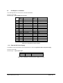
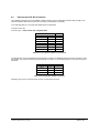
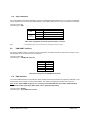
1
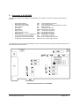
EB 200P
.
Evaluation Board ERTEC 200P
Manual
Copyright © Siemens AG 2013. All rights reserved.
Technical data subject to change
1
EB 200P Manual
Version 1.0.1
Edition (09/2013)
Disclaimer of Liability
We have checked the contents of this manual for agreement with the hardware and software
described. Since deviations cannot be precluded entirely, we cannot guarantee full agreement.
However, the data in this manual are reviewed regularly. Necessary corrections are included in
subsequent editions. Suggestions for improvement are welcomed.
Copyright
© Siemens AG 2012. All rights reserved
The reproduction, transmission or use of this document or its contents is not permitted without
express written authority. Offenders will be liable for damages. All rights, including rights created
by patent grant or registration of a utility model or design, are reserved.
All product and system names are registered trademarks of their respective owner and must be
treated as such.
Technical data subject to change.
Copyright © Siemens AG 2013. All rights reserved.
Technical data subject to change
2
EB 200P Manual
Version 1.0.1
Preface
Contents of this Manual
Detailed description of the individual function groups of the EB 200P
Connector pin assignment and jumper assignment
Target Audience of this Manual
This manual is intended for hardware developers who want to use the ERTEC 200P for new products. Experience
working with processors and designing embedded systems and knowledge of Ethernet are required for this.
The manual serves as a reference for software developers. Sections 7 and 8 describe the jumper settings and
connectors that are required for software tests (e.g. debugging, terminal outputs, etc.).
Structure of this Manual
This manual describes the ERTEC 200P evaluation board. The manual is structured as follows:
o
Section 1 Introduction
o
Section 2 Hardware Structure of the EB 200P
o
Section 3 Memory Distribution of the EB 200P
o
Section 4 Operating Modes of the EB 200P
o
Section 5 JTAG Interface of the EB 200P
o
Section 6 Settings of the EB 200P
o
Section 7 Connectors of the EB 200P
o
Section 8 Jumpers of the EB 200P
o
Section 9 Mechanical Structure of the EB 200P
o
Section 10 List of Terms and References
When working with modules, always take precautionary measures against electrostatic charge
(ESD – Electrostatic Sensitive Devices).
For module handling and installation, refer to /1/.
This manual will be updated as required. You can find the current version of the manual on the Internet at
http://www.siemens.com/comdec .
Copyright © Siemens AG 2013. All rights reserved.
Technical data subject to change
3
EB 200P Manual
Version 1.0.1
Guide
To help you quickly find the information you need, this manual contains the following aids:
o
A complete table of contents as well as a list of all figures and tables in the manual are provided at the beginning
of the manual.
o
A glossary containing definitions of important terms used in the manual is located following the appendices.
o
References to other documents are indicated by the document reference number enclosed in slashes (/No./). The
complete title of the document can be obtained from the list of references at the end of the manual.
Additional Support
If you have questions regarding use of the described block that are not addressed in the documentation, please
contact your Siemens representative.
Please send your written questions, comments, and suggestions regarding the manual to the hotline via the e-mail
address indicated above.
In addition, you can receive general information, current product information, FAQs, and downloads pertaining to your
application on the Internet at:
http://www.siemens.com/comdec
Technical Contacts for Germany / Worldwide
Siemens AG
Automation & Drives
ComDeC
Phone:
Phone:
Fax:
E-mail:
0911/750-2736
0911/750-2080
0911/750-2100
ComDeC@siemens.com
Street address:
Mailing address:
Würzburgerstr.121
P.O. Box 2355
90766 Fürth
Federal Republic of Germany
90713 Fürth
Federal Republic of Germany
Technical Contacts for USA
PROFI Interface Center:
One Internet Plaza
PO Box 4991
Johnson City, TN 37602-4991
Tel.: +1 (423) - 262 - 2576
Fax: +1 (423) - 262 - 2103
Mail: pic.industry@siemens.com
Copyright © Siemens AG 2013. All rights reserved.
Technical data subject to change
4
EB 200P Manual
Version 1.0.1
Contents
1
Introduction .................................................................................................................................. 8
1.1
1.2
1.3
1.4
2
Procedure when using ERTEC 200P to develop your own PROFINET IO Device .................................. 8
Structure of the EB 200P .............................................................................................................................. 9
Features of the EB 200P .............................................................................................................................. 9
Block Diagram of the EB 200P..................................................................................................................... 10
Hardware Structure of the EB 200P ......................................................................................... 11
2.1 ERTEC 200P ................................................................................................................................................. 11
2.1.1 Function Overview .................................................................................................................................. 11
2.1.2 Operating Modes of the EB 200P .......................................................................................................... 12
2.1.3 Boot Modes of the EB 200P ................................................................................................................... 13
2.1.4 ERTEC 200P Processor and I/O ............................................................................................................ 13
2.1.5 PNIP 14
2.1.6 External Memory Controller (EMC) ........................................................................................................ 14
2.1.7 Debug and Trace Interface ..................................................................................................................... 14
2.1.8 General Purpose Interface (GPIO)......................................................................................................... 15
2.2 Memory on EB 200P ..................................................................................................................................... 18
2.2.1 SDRAM .................................................................................................................................................... 18
2.2.2 Burst Mode FLASH ................................................................................................................................. 18
2.2.3 I2C EEPROM .......................................................................................................................................... 18
2.3 Test and debug peripherals .......................................................................................................................... 19
2.3.1 Status LEDs............................................................................................................................................. 19
2.3.2 Synchronization output and input ........................................................................................................... 20
2.3.3 SPI temperature sensor .......................................................................................................................... 20
2.3.4 User GPIOs with LEDs and switch......................................................................................................... 21
2.3.5 UART over USB ...................................................................................................................................... 21
2.4 Reset System of the EB 200P ...................................................................................................................... 22
2.4.1 Reset Button ............................................................................................................................................ 22
2.4.2 PCI Express Reset .................................................................................................................................. 22
2.4.3 Watchdog and Software Reset............................................................................................................... 22
2.5 Clock System of the EB 200P ...................................................................................................................... 23
2.5.1 Clock Source of PCI Express Interface ................................................................................................. 23
2.5.2 Clock Source of EB 200P via a Quartz Crystal ..................................................................................... 23
2.6 Ethernet Interfaces of the EB 200P ............................................................................................................. 24
2.6.1 Ethernet ports (X1) .................................................................................................................................. 24
2.6.2 TAP ports (X1)......................................................................................................................................... 24
2.6.3 POF Transceiver ports (X3, X4) ............................................................................................................. 24
3
Memory Allocation of EB 200P ................................................................................................. 25
3.1 Memory Mapping .......................................................................................................................................... 25
4
Operating Modes of the EB 200P.............................................................................................. 26
4.1 Operating the EB 200P without programmed Flash ................................................................................... 26
4.2 Operating the EB 200P with programmed Flash......................................................................................... 26
4.3 Operating the EB 200P in XHIF Mode ......................................................................................................... 26
5
6
Debug/ Boundary scan Interface .............................................................................................. 27
Connectors of the EB 200P ....................................................................................................... 28
6.1 PCI Express x1 Interface .............................................................................................................................. 29
6.2 External DC Power Supply ........................................................................................................................... 29
6.3 Ethernet and TAP RJ-45 interface ............................................................................................................... 30
6.4 Sync connector.............................................................................................................................................. 31
6.5 USB-UART Interface..................................................................................................................................... 31
6.6 EMC interface................................................................................................................................................ 31
6.7 User GPIO [15 to 0] ...................................................................................................................................... 33
6.8 JTAG connector for FPGA............................................................................................................................ 34
6.9 GPIO [95 to 0] connectors ............................................................................................................................ 34
6.10 Trace connector for ETM of ARM926EJ-S .................................................................................................. 36
6.11 JTAG connector for ICE or debugger .......................................................................................................... 37
Copyright © Siemens AG 2013. All rights reserved.
Technical data subject to change
5
EB 200P Manual
Version 1.0.1
6.12 Configuration pins for ERTEC 200P ............................................................................................................ 38
6.13 Configuration pins for onboard circuits ........................................................................................................ 39
7
8
Settings on the EB 200P............................................................................................................. 42
Structure of the EB 200P............................................................................................................ 44
8.1 Mechanical Structure .................................................................................................................................... 44
8.2 Front and Display Element ........................................................................................................................... 44
8.3 Description of LEDs on the slot bracket....................................................................................................... 44
9
Miscellaneous .............................................................................................................................. 45
9.1 Acronyms/Glossary: ...................................................................................................................................... 45
9.2 References: ................................................................................................................................................... 46
Copyright © Siemens AG 2013. All rights reserved.
Technical data subject to change
6
EB 200P Manual
Version 1.0.1
List of Figures
Figure 1: EB 200P with connected debugger........................................................................................................................ 9
Figure 2: Block diagram of EB 200P.................................................................................................................................... 10
Figure 3 Status LEDs on the card bracket .......................................................................................................................... 19
Figure 4 RESET system diagram ........................................................................................................................................ 22
Figure 5 Connector Positions on the EB 200P ................................................................................................................... 28
Figure 6 EB 200P default configuration of ERTEC 200P ................................................................................................... 42
Figure 7 EB 200P default configuration of onboard circuits ............................................................................................... 43
Figure 8 EB 200P slot bracket view ..................................................................................................................................... 44
List of Tables
Table 1 Selection of Operating Modes and System Functions for EB 200P ..................................................................... 12
Table 2 Test and debug jumpers configuration ................................................................................................................... 13
Table 3 Boot mode selection for EB200P ........................................................................................................................... 13
Table 4 CS Areas of the EB 200P ....................................................................................................................................... 14
XHIF when CFG(6:3) = depending on XHIF Mode see Table 1 ................................................................................. 15
XHIF when CFG(6:3) = depending on XHIF Mode see Table 1 ................................................................................. 15
Table 5 Test circuits interconnections on EB 200P ............................................................................................................ 16
Table 6 Debug circuits interconnections on EB 200P ........................................................................................................ 17
Table 7 I2C EEPROM connection ....................................................................................................................................... 18
Table 8 Status LEDs connection.......................................................................................................................................... 20
Table 9 Synchronization input/output connection ............................................................................................................... 20
Table 10 SPI temperature sensor connection ..................................................................................................................... 20
Table 11 User GPIO connection .......................................................................................................................................... 21
Table 12 USB UART convertor connection ......................................................................................................................... 21
Table 13 Ethernet ports pinout............................................................................................................................................. 24
Table 14 TAP ports pinout.................................................................................................................................................... 24
Table 15 EB 200P memory mapping................................................................................................................................... 25
Table 16 Pin assignment of PCIe interface ......................................................................................................................... 29
Table 17 Pin assignment of external power supply connector........................................................................................... 29
Table 18 Pin assignment of Ethernet connectors ............................................................................................................... 30
Table 19 Pin assignment of TAP connectors ...................................................................................................................... 30
Table 20 Pin assignment of external synchronization connector...................................................................................... 31
Table 21 Pin assignment of USB Mini-B connector ............................................................................................................ 31
Table 22 Pin assignment of EMC connector X80 ............................................................................................................... 32
Table 23 Pin assignment of EMC connector X81 ............................................................................................................... 33
Table 24 Pin assignment of GPIO connector X50 .............................................................................................................. 34
Table 25 Pin assignment of FPGA JTAG connector X32.................................................................................................. 34
Table 26 Pin assignment of GPIO connector X20 .............................................................................................................. 35
Table 27 Pin assignment of GPIO connector X21 .............................................................................................................. 36
Table 28 Pin assignment of GPIO connector X22 .............................................................................................................. 36
Table 29 Pin assignment of TRACE connector X30 ........................................................................................................... 37
Table 30 Boot mode settings of ERTEC 200P.................................................................................................................... 38
Table 31 Configuration settings of ERTEC 200P................................................................................................................ 39
Table 32 ERTEC 200P configuration header pinout........................................................................................................... 39
Table 33 EB 200P FPGA XHIF settings .............................................................................................................................. 40
Table 34 Test and debug circuits settings ........................................................................................................................... 40
Table 35 EB 200P board settings header pinout ................................................................................................................ 41
Copyright © Siemens AG 2013. All rights reserved.
Technical data subject to change
7
EB 200P Manual
Version 1.0.1
1
Introduction
This manual describes the procedure for using the ERTEC 200P for HW development of a PROFINET IO device and
the properties of the EB 200P evaluation board.
The intended use of the EB 200P evaluation board is as follows:
It serves as a template for development of your own PROFINET IO device hardware.
It supports development and testing of your own PROFINET IO device application software.
It enables testing of your hardware on a supplementary board together with the EB 200P, where applicable.
1.1
Procedure when using ERTEC 200P to develop your own PROFINET IO Device
If you are using the recommended minimum configuration for a PROFINET IO device, no changes (or only minor
changes) have to be made in the board support package (BSP) for your additionally required hardware. The board
support package adapts the operating system to the hardware.
Procedure
You can use ERTEC 200P to develop your own hardware in one of two ways:
o By using a test board on the EB 200P to adapt and test your application circuit
o By using ERTEC 200P directly to develop and test your complete target hardware
Note the following boundary conditions for hardware development:
Debug interfaces for commissioning and testing
Always make provision for connectors on your hardware to the JTAG interface and, if possible, to a USB virtual serial
interface (UART) of the ERTEC 200P in order to facilitate commissioning.
Copyright © Siemens AG 2013. All rights reserved.
Technical data subject to change
8
EB 200P Manual
Version 1.0.1
1.2
Structure of the EB 200P
The EB 200P is implemented in the form of a half-size PCI Express card. The PCI Express interface is used only for
PC mode. In standard configuration the EB 200P is operated as a stand-alone module. The EB 200P is supplied by
means of an external plug-in power supply (part of the development kit).For software debugging a JTAG interface is
available, for more information about JTAG interface is in Chapter 5.
Figure 1: EB 200P with connected debugger
1.3
Features of the EB 200P
In addition to the ERTEC 200P with its integrated function groups, the following elements are available on the
EB 200P:
PC front panel element with
o 2 RJ45 PROFINET sockets with integrated magnetics, with POF assembly option
o 2 RJ45 TAP sockets for debugging purposes during development for MDI port
o 2 LEDs Link and Activity per RJ45 socket
o 4 LEDs for additional status indicators
o BNC connector for PLL Sync signal
Flash memory
32 Mbytes, Burst Mode, 2 chips 1Mx16bit in parallel
SDRAM
128 Mbytes, 2chips 32Mx16bit in parallel
I2C EEPROM
SPI temperature sensor
Debug and trace interface for ARM926EJ-S Microcontroller
USB Virtual serial interface for monitoring
Configuration and boot modes can be set via jumpers
Various operating modes of the EB 200P can be set via jumpers
Various connectors for external wiring
Copyright © Siemens AG 2013. All rights reserved.
Technical data subject to change
9
EB 200P Manual
Version 1.0.1
1.4
Block Diagram of the EB 200P
Figure 2: Block diagram of EB 200P
Copyright © Siemens AG 2013. All rights reserved.
Technical data subject to change
10
EB 200P Manual
Version 1.0.1
2
Hardware Structure of the EB 200P
2.1
ERTEC 200P
2.1.1
Function Overview
Refer to documents /1/ and /2/ for a detailed function description of the ERTEC 200P.
In this manual, only the main components are described briefly and represented in a block diagram.
The following four AHB masters are integrated in the ERTEC 200P:
ARM926EJ-S with trace/debug port and high-performance interrupt controllers
PNIP with 64 Kbytes of K-RAM for real-time Ethernet communication
External host processor on the XHIF interface
32-channel DMA controller
The following I/O blocks are available to the masters:
External memory controller (EMC) with SDRAM and SRAM controller
Two Ethernet interfaces with integrated MII PHYs
Blocks connected to APB bus
96-bit GPIO
4x UART
2x SPI
2
3x I C
6 timers
F-timer
2x Watchdog
Boot ROM
System Control
Peripherie Interface
I-Filter
The multi-layer AHB bus system enables a largely independent operation of the masters. Internal arbitration logic
prevents access conflicts if multiple masters want to access the same I/O block. The function groups of the ERTEC
200P are shown in block diagram. For block diagram please refer to /1/
Copyright © Siemens AG 2013. All rights reserved.
Technical data subject to change
11
EB 200P Manual
Version 1.0.1
2.1.2
Operating Modes of the EB 200P
Various configurations on the EB 200P can be set by means of jumpers X40.9/10 and X41.1/2. These jumpers are
described in Section 7. The following configuration settings are possible on the ERTEC 200P.
Boot configuration
Cfg(6)
Cfg(5)
Cfg(4)
Cfg(3)
Cfg(2)
Cfg(1)
Cfg(0)
REF_CLK Tristate
x
x
x
x
x
x
Open
REF_CLK Output (25MHz)
x
x
x
x
x
x
Close
ARM Clock 125MHz
x
x
x
x
x
Close
x
ARM Clock 250MHz
x
x
x
x
x
Open
x
PLL Bypass on (Config(1) = Close)
x
x
x
x
Close
x
x
PLL Bypass off
x
x
x
x
Open
x
x
XHIF=16bit, XHIF_XWR = R/W
Close
Open
x
Close
x
x
x
XHIF=16bit, XHIF_XWR, XHIF_XWR separated
Close
Open
x
Open
x
x
x
XHIF=16bit, XHIF_XRDY active high
Close
Open
Open
x
x
x
x
XHIF=16bit, XHIF_XRDY active low
Close
Open
Close
x
x
x
x
XHIF=32bit, XHIF_XWR = R/W
Close
Close
x
Close
x
x
x
XHIF=32bit, XHIF_XWR, XHIF_XWR separated
Close
Close
x
Open
x
x
x
XHIF=32bit, XHIF_XRDY active high
Close
Close
Open
x
x
x
x
XHIF=32bit, XHIF_XRDY active low
Close
Close
Close
x
x
x
x
XHIF=off
Open
Open
Open
Open
x
x
x
XHIF=off, ARM926 Trace Port on
Open
Close
Close
Close
x
x
x
x
x
x
Remaining combinations
XHIF=off
Table 1 Selection of Operating Modes and System Functions for EB 200P
XHIF mode: Cfg(6) jumper closed
The XHIF interface is active for access of a host processor system to internal components of the ERTEC 200P.
Trace mode: Cfg(6) open, Cfg(5) close, Cfg(4) close, Cfg(3) close
The trace port is available to the user in this mode.
Copyright © Siemens AG 2013. All rights reserved.
Technical data subject to change
12
EB 200P Manual
Version 1.0.1
Following table shows configuration jumpers for test and debugging. Pin headers are labeled X42 and X43.
Function
Signal
Sync(0)
BNC tip pin
1
2
ERTEC GPIO(9)
Function when
jumper is installed
Sync BNC Input
Sync(1)
BNC tip pin
3
4
ERTEC GPIO(0)
Sync BNC Output
Trace CS bus switch OE
5
6
GND
Trace Disabled
EEPROM CS bus switch OE
7
8
GND
EEPROM Enabled
GPIOs Enabled
Trace
EEPROM
User GPIOs
Pin Pin
Signal
User GPIOs CS bus switch OE
9
10
GND
UART
UART CS bus switch OE
11
12
GND
UART Enabled
TEMP
TEMP CS bus switch OE
13
14
GND
SPI Sensor Enabled
F_XHIF(0)
FPGA_CONFIG(0)
15
16
GND
F_XHIF(1)
FPGA_CONFIG(1)
17
18
3.3V
F_XHIF(2)
FPGA_CONFIG(2)
19
20
3.3V
F_XHIF(3)
FPGA_CONFIG(3)
21
22
GND
None
NC
23
24
NC
None
NC
25
26
NC
None
NC
27
28
NC
None
NC
29
30
NC
Same functionality as
Cfg(3)-Cfg(6)
Table 2 Test and debug jumpers configuration
2.1.3
Boot Modes of the EB 200P
Various boot modes on the EB 200P can be set by means of jumpers X40.1/2 to X40.7/8.
The following boot modes are supported:
Boot source
Boot(3)
Boot(2)
Boot(1)
NOR Flash (8bit)
Open
Open
Close
Boot(0)
Open
NOR Flash (16bit)
Open
Open
Close
Close
NOR Flash (32bit)
Open
Open
Open
Open
XHIF
Open
Close
Open
Close
Table 3 Boot mode selection for EB200P
2.1.4
ERTEC 200P Processor and I/O
The ARM926EJ-S processor with interrupt controller is integrated in the ERTEC 200P. The processor and various
standard I/O are available to users for their applications. These include the following function groups:
ARM926EJ-S processors with
125/250 MHz operating frequency that can be set via jumpers (see Operating Modes 2.1.2)
16 Kbytes of instruction cache
16 Kbytes of data cache
256 Kbytes of data TCM
JTAG interface for debug interface
Interrupt controller for asynchronous events (96 IRQ and 8 FIQ inputs)
SDRAM controller 125 MHz/max. 256 Mbytes of address space (16/32-bit data width can be assigned)
SRAM controller, up to 4 x 16 Mbytes (8/16/32-bit data width and timing can be assigned separately for all 4
areas)
2x Watchdog timer unit for monitoring module functions
Timer unit for generating periodic trigger pulses
F-timer for fail-safe applications
GPIO ports for activating LEDs, etc.
SPI interface for connecting serial EEPROM/Flash
4x UART
Copyright © Siemens AG 2013. All rights reserved.
Technical data subject to change
13
EB 200P Manual
Version 1.0.1
3x I2C
2.1.5
PNIP
The PNIP provides the required function for PROFINET IO. It contains the following functions:
Configuration register for PNIP
64 Kbytes of K-RAM for RT and IRT communication
2.1.6
External Memory Controller (EMC)
EMC comprises of 2 different controllers, one supporting the SDRAM Memory devices (including Mobile SDRAM), the
other supporting asynchronous SRAM timing in different flavors, including Burst Flash ROM memory devices.
SDRAM-Controller features:
16/32 Bit databus width
PC133 SDRAM-compatible (125 MHz synchron is used in ERTEC 200P)
1 Bank with max. 256 MByte SDRAM (32 Bit databus)
SDRAM support for following parts:
o CAS-Latency: 2 or 3 clocks
o Bank-address bits (1/2/4 internal banks), realized via the lowest two bits of the address bus MA(1:0)
o 8/9/10/11 bits column-address MA(13), MA(11:2)
o max. 14 bits row-address MA(15:2)
Asynchronous Controller features:
Can be set to 8/16/32-bit data bus width (for each chip select programmable) chip selects
The timing for each chip select can be set individually
The response to ready signal can be set individually for each chip select
The default setting is slow timing for booting purposes
A maximum of 64 MB address area for each chip select
Acknowledgement delay monitoring for external components can be set by software
The boot medium is always expected on chip select signal XCS_PER0. EB 200P board is equipped with Burst Mode
FLASH connected to this CS signal. If extension board is used, one can reconnect chip select signals from the default
state to extension board by changing of resistors. The following blocks of the EB 200P can be selected with the chipselect lines:
Chip Select
XCS_PER0
XCS_PER1
XCS_PER2
XCS_PER3
I/O
Boot Flash / FLASH
reserved
extension board
extension board
Function
2x 8Mbit x 16
8kbit x 32
16Mbit x 32
16Mbit x 32
Table 4 CS Areas of the EB 200P
2.1.7
Debug and Trace Interface
The ETM macro cell of the ARM926EJ-S can be used as a debug and trace interface in the ERTEC 200P. With this
interface, the user software running on the ARM926EJ-S and the user data can be analyzed and traced. The ETM
module is a standard module recommended by ARM on which various available debuggers can be run. If the trace
interface is used, the XHIF interface is not available (configuration setting "Trace On“, see Section 2.1.2). If the trace
interface is used, the required parameter assignment of the ETM macro cell must be performed with the debugger, so
that the required pins are switched to trace functionality.
For debug and trace functionality 38pin MICTOR connector is assembled on EB 200P. JTAG pins on MICTOR are
directly connected to JTAG interface on ERTEC 200P. Signals for tracing can be connected or disconnected to/from
ERTEC 200P GPIOs by bidirectional bus switch
The ETM macro cell is described in documents /9/ and /10/.
Copyright © Siemens AG 2013. All rights reserved.
Technical data subject to change
14
EB 200P Manual
Version 1.0.1
2.1.8
General Purpose Interface (GPIO)
The GPIO interface of the ERTEC 200P consists of 96 I/O that can be configured for different functionality. GPIO(150) pins have interrupt capability.
Pins can be split to several groups regarding configuration jumpers:
GPIO(31-0) : GPIO except when CFG(6:3) = “1100”
GPIO(63-32) :
XHIF when CFG(6:3) = depending on XHIF Mode see Table 5
TRACE port when CFG(6:3) = “1110”
otherwise GPIO
GPIO(95-64) :
XHIF when CFG(6:3) = depending on XHIF Mode see Table 6
TRACE port when CFG(6:3) = “1110”
The following tables describe the interconnections between test and debug circuits and ERTEC 200P. Not all
components can be connected or disconnected from ERTEC GPIOs.
Status LED
NAND
FLASH
BNC
Sync
RS485
Sync
I2C
EEPROM
SPI Temp
Configuration
by bus
switch
no
yes
no
no
yes
yes
Configuration
by jumper
no
no
yes
no
no
no
GPIO(0)
-
-
Sync
Out*1
D*2
-
-
GPIO(1)
-
-
-
-
-
-
GPIO(2)
-
-
-
-
-
-
GPIO(3)
-
-
-
-
-
-
GPIO(4)
-
-
-
-
GPIO(5)
-
-
-
-
GPIO(6)
-
-
-
-
GPIO(7)
-
-
-
-
-
-
GPIO(8)
-
-
-
-
-
-
GPIO(9)
-
-
Sync
In*1
R*2
-
-
GPIO(10)
-
R/XB
-
-
-
-
GPIO(11)
-
-
-
-
-
-
GPIO(12)
-
-
-
-
-
-
GPIO(13)
-
-
-
-
-
-
GPIO(14)
-
-
-
-
I2C_SCLK
-
GPIO(15)
-
-
-
-
I2C_SDOI
-
GPIO(16)
-
-
-
DE*2
-
SPI_SCLKOUT
GPIO(17)
-
-
-
XRE*2
-
SPI_SFRMOUT
GPIO(18)
-
-
-
-
-
-
GPIO(19)
-
-
-
-
-
SPI_SSPRXD
GPIO(20)
-
-
-
-
-
-
GPIO(21)
-
-
-
-
-
-
GPIO(22)
-
-
-
-
-
-
GPIO(23)
-
-
-
-
-
-
GPIO(23)
-
-
-
-
-
-
Copyright © Siemens AG 2013. All rights reserved.
Technical data subject to change
15
-
-
EB 200P Manual
Version 1.0.1
GPIO(24)
-
-
-
-
-
-
GPIO(25)
Error
-
-
-
-
-
GPIO(26)
Maintenance
-
-
-
-
-
GPIO(27)
Diagnostic
-
-
-
-
-
GPIO(28)
ProfiEnergy
-
-
-
-
-
GPIO(29)
Sync
-
-
-
-
-
GPIO(30)
FO-1
-
-
-
-
-
GPIO(31)
FO-2
XCE
-
-
-
-
Table 7 Test circuits interconnections on EB 200P
Switch
LEDs
User GPIOs
UART*3
Debug
FPGA
POFs
Configuration
by bus switch
yes (shared)
yes
no
no
no
Configuration
by jumper
no
no
no
no
no
GPIO(0)
SW0
LED0
user GPIO0
-
-
-
-
GPIO(1)
SW1
LED1
user GPIO1
-
-
-
-
GPIO(2)
SW2
LED2
user GPIO2
-
-
-
-
GPIO(3)
SW3
LED3
user GPIO3
-
-
-
-
GPIO(4)
SW4
LED4
user GPIO4
-
-
-
POF1_SDOI
GPIO(5)
SW5
LED5
user GPIO5
-
-
-
POF1_SCLK
GPIO(6)
SW6
LED6
user GPIO6
-
-
-
POF2_SDOI
GPIO(7)
SW7
LED7
user GPIO7
-
-
-
POF2_SCLK
GPIO(8)
-
-
-
-
-
XINT
-
GPIO(9)
-
-
-
-
-
-
-
GPIO(10)
-
-
-
-
DBACK
-
-
GPIO(11)
-
-
-
-
DBGRQ
-
-
GPIO(12)
-
-
-
CTS
-
-
-
GPIO(13)
-
-
-
RTS
-
XWD
OUT
-
GPIO(14)
-
-
-
TXD
-
-
-
GPIO(15)
-
-
-
RXD
-
-
-
GPIO(16)
-
LED8
user GPIO8
-
-
-
-
GPIO(17)
-
LED9
user GPIO9
-
-
-
-
GPIO(18)
-
LED10
user GPIO10
-
-
-
-
GPIO(19)
-
LED11
user GPIO11
-
-
-
-
GPIO(20)
-
LED12
user GPIO12
-
-
-
-
GPIO(21)
-
LED13
user GPIO13
-
-
-
-
GPIO(22)
-
LED14
user GPIO14
-
-
-
-
GPIO(23)
-
LED15
user GPIO15
-
-
-
-
GPIO(23)
-
-
-
-
-
-
-
GPIO(24)
-
-
-
-
-
-
-
GPIO(25)
-
-
-
-
-
-
-
GPIO(26)
-
-
-
-
-
-
-
Copyright © Siemens AG 2013. All rights reserved.
Technical data subject to change
16
EB 200P Manual
Version 1.0.1
GPIO(27)
-
-
-
-
-
-
-
GPIO(28)
-
-
-
-
-
-
-
GPIO(29)
-
-
-
-
-
-
-
GPIO(30)
-
-
-
-
-
-
-
GPIO(31)
-
-
-
-
-
-
-
Table 8 Debug circuits interconnections on EB 200P
Note:
*1 Configured by jumper at one time can be connected only input or output
*2 Assembly option, shared pins with BNC connector, if assembled BNC must not be used or connected
*3 UART means connection via USB - Serial convertor
*4 DBACK and DBGRQ can be configured by jumper only on TRACE connector, on the JTAG connector
are connected always
Copyright © Siemens AG 2013. All rights reserved.
Technical data subject to change
17
EB 200P Manual
Version 1.0.1
2.2
Memory on EB 200P
The following memory types are available on the EB 200P evaluation board:
2.2.1
SDRAM
The SDRAM interface consists of 2 Micron type MT48H32M16LFBF-75IT blocks.
128-Mbyte memory capacity
32-bit data width
133 MHz clock frequency
2.2.2
Burst Mode FLASH
The Flash interface consists of 2 Spansion type S29WS128P0PBAW00 blocks.
32-Mbyte memory capacity
32-bit data width
66 MHz maximum frequency
2.2.3
I2C EEPROM
Small 2kB I2C EEPROM is connected to ERTEC 200P GPIOs via bidirectional bus switch. Memory can be connected
or disconnected by configuration jumper. The following table describes connection between memory pins and
ERTEC’s
GPIOs (via bus switch).
Signal
E0
Signal function
Connection
Chip address bit 0
Pull down
Note
1k
E1
Chip address bit 1
Pull down
1k
E2
Chip address bit 2
Pull down
SDA
Data
GPIO(15)
4.7k
pull up to 3.3V
SCL
XWC
Clock
GPIO(14)
4.7k
pull up to 3.3V
Write enable
Pull down
1k
1k
Table 9 I2C EEPROM connection
Copyright © Siemens AG 2013. All rights reserved.
Technical data subject to change
18
EB 200P Manual
Version 1.0.1
2.3
Test and debug peripherals
For easier development some test and debug circuits are assembled on board. Test and debug circuit can be
selectively connected to ERTEC 200P GPIOs. Configuration is done by jumpers and details about configuration are
described in chapter 6.13. All test and debug circuits are connected to GPIOs which are using 3.3V logic.
2.3.1
Status LEDs
Two groups of status LEDs are integrated on EB200P. The first group is near the bracket with small holes.
Figure 3 Status LEDs on the card bracket
The second group of LEDs is assembled on the EB200P top edge. The following table describes connection to
ERTEC 200P GPIOs. LEDs are not powered directly from GPIOs but via buffers at 3.3V .
Copyright © Siemens AG 2013. All rights reserved.
Technical data subject to change
19
EB 200P Manual
Version 1.0.1
Function
Color
Position
Connection
Sync
Green
Bracket
GPIO(29)
Resistor
P
Green
Bracket
PSU
750
MT
Yellow
Bracket
GPIO(26)
750
Error
Red
Bracket
GPIO(25)
750
Power
Green
PCB
PSU
750
750
Error
Red
PCB
GPIO(25)
750
Maintenance
Yellow
PCB
GPIO(26)
750
Diagnostic
Yellow
PCB
GPIO(27)
750
PROFIenergy
Green
PCB
GPIO(28)
750
Sync
Green
PCB
GPIO(29)
750
FO-1
Yellow
PCB
GPIO(30)
750
FO-2
Yellow
PCB
GPIO(31)
750
Table 10 Status LEDs connection
Status LEDs can not be disconnected from GPIOs by any configuration jumper. Configuration is fixed.
2.3.2
Synchronization output and input
For measurement of delays during synchronized state, external connectors are assembled. Two types of connectors
with different electrical functionality can be used.
The first one is BNC connector available on the bracket. This connector is unidirectional and cannot be used for both
ways at one time. Direction will be switched by jumper to achieve zero delay (no switch, no buffer).
The second possibility is a three pin connector like it is used on EB 200. Connector is connected to ERTEC GPIOs via
RS485 interface. Direction is controlled by ERTEC 200P.
Connection is described in the following table. For RS485 input output is described convertor connection. Connector
pin out is described in chapter 2.1.2.
Connector/Convertor
Connection
Note
GPIO(9)
Configuration via jumper
Out
GPIO(0)
Configuration via jumper
R
GPIO(9)
In
BNC
D
GPIO(0)
DE
GPIO(16)
XRE
GPIO(17)
RS485
Table 11 Synchronization input/output connection
2.3.3
SPI temperature sensor
Simple SPI temperature sensor is connected to ERTEC 200P GPIOs via bidirectional bus switch (SN74CB3Q3384). A
SPI sensor can be connected or disconnected by configuration jumper. The following table describes the connection
between sensor pins and ERTEC’s GPIOs (via bus switch).
Signal
SO
SCK
XCS
Signal function
Connection
Data out
SPI_SSPRXD(1a) GPIO(19)
Clock
SPI_SCLKOUT(1a) GPIO(16)
Chip select
SPI_SFRMOUT(1a) GPIO(17)
Note
Pull down 1k
Pull down 1k
Pull up 1k
to 3.3V
Table 12 SPI temperature sensor connection
Copyright © Siemens AG 2013. All rights reserved.
Technical data subject to change
20
EB 200P Manual
Version 1.0.1
2.3.4
User GPIOs with LEDs and switch
16 GPIOs are available for the user via 2x10 pin header. GND and 3.3V pins are available on this pin header too.
These 16 pins can be connected or disconnected to/from ERTEC 200P GPIOs by bidirectional bus switch
(SN74CB3Q3384). Pin out for pin header and jumper configuration for test and debug circuits are described in chapter
2.1.2. To each GPIO available on pin header a LED is connected via buffer (SN74ALVCH16244DGGR). If pins are
connected to ERTEC and output direction is set the LED will signalize output state. If input direction is selected the
LED will signalize input signal. Octal slide switch is connected to user GPIO(0..7). The opposite contact of slide switch
is connected to 3.3V (via 470 protection resistor for each slide switch). The following table describes connections
between user GPIO pin header and ERTEC’s GPIOs (via bus switch).
User pin
GPIO0
Connection
GPIO(0)
Pull down
4.7k
Switch
SW0
GPIO1
GPIO(1)
4.7k
SW1
GPIO2
GPIO(2)
4.7k
SW2
GPIO3
GPIO(3)
4.7k
SW3
GPIO4
GPIO(4)
4.7k
SW4
GPIO5
GPIO(5)
4.7k
SW5
GPIO6
GPIO(6)
4.7k
SW6
GPIO7
GPIO(7)
4.7k
SW7
GPIO8
GPIO(16)
4.7k
None
GPIO9
GPIO(17)
4.7k
None
GPIO10
GPIO(18)
4.7k
None
GPIO11
GPIO(19)
4.7k
None
GPIO12
GPIO(20)
4.7k
None
GPIO13
GPIO(21)
4.7k
None
GPIO14
GPIO(22)
4.7k
None
GPIO15
GPIO(23)
4.7k
None
Table 13 User GPIO connection
2.3.5
UART over USB
For debug purposes the UART-USB convertor is integrated on board. The TUSB3410 from TI is used. Connection
with ERTEC is described in the following table. USB-UART convertor can be connected or disconnected to/from
ERTEC by bidirectional bus switch. Configuration is done by jumper.
Signal
SIN
Signal function
Dir
Connection
Data
In
TXD(2) GPIO(14)
SOUT
Data
Out
RXD(2) GPIO(15)
RTS
CTS
Ready to send
Out
CTS(2) GPIO (12)
Clear to send
In
RTS(2) GPIO(13)
Note
Pull up 10k
to 3.3V
Pull up 10k
to 3.3V
Table 14 USB UART convertor connection
Assigned USB identification IDs:
USB PID = 0x040E
USB VID = 0x0908
Note: EB200P must be powered prior plugging USB cable in PC USB port.
Copyright © Siemens AG 2013. All rights reserved.
Technical data subject to change
21
EB 200P Manual
Version 1.0.1
2.4
Reset System of the EB 200P
The reset system of the EB 200P has 4 reset paths:
Power On Reset:
This reset is generated during power up on the EB 200P. The RESET_N signal affects the following function
units.
Resetting of ERTEC 200P logic
Resetting of the PCI Express side
Resetting of the Page Mode Flash
Resetting of the Burst Mode Flash
PCI Express Reset:
If the EB 200P is operated with an active host, the connected host reset signal resets just the PCI Express
interface. ERTEC 200P is not reset. This must be done later in the host software.
Resetting the Debug Interface:
The debug interface is linked to the two reset signals SRST_N and TRST_N of the EB 200P. This enables the
debugger to initiate and monitor the reset of the following function groups.
Host software Reset
ERTEC 200P can be reset through software running on the host PC.
The hardware reset remains active for at least 20 ms following power up.
Figure 4 RESET system diagram
2.4.1
Reset Button
The EB 200P has a reset button that initiates a manual reset of the ERTEC 200P BM Flash and PM Flash without
disconnecting the voltage supply.
2.4.2
PCI Express Reset
In PCI Express host mode, the host reset controls the evaluation board directly.
2.4.3
Watchdog and Software Reset
Additional reset events can be initiated by the watchdog or software reset. Both reset events have the same effect as
a debug reset.
Copyright © Siemens AG 2013. All rights reserved.
Technical data subject to change
22
EB 200P Manual
Version 1.0.1
2.5
Clock System of the EB 200P
2.5.1
Clock Source of PCI Express Interface
The PCI Express bus supplies the on-board FPGA of the EB 200P with its clock. From this signal, system clock for
FPGA of 125MHz is synthesized. If EB200P is working in standalone mode there is no clock source for FGPA.
2.5.2
Clock Source of EB 200P via a Quartz Crystal
By default, a 25 MHz quartz crystal supplies the EB 200P via the ERTEC. Quartz tolerance is 15ppm
The sum of the deviation from aging, temperature, voltage, vibration and shock for ERTEC 200P clocks should not
exceed 100ppm.
Copyright © Siemens AG 2013. All rights reserved.
Technical data subject to change
23
EB 200P Manual
Version 1.0.1
2.6
2.6.1
Ethernet Interfaces of the EB 200P
Ethernet ports (X1)
Two 100Mbit/s full duplex ports are available in ERTEC 200P. PHYs are integrated in ERTEC 200P package. Only
external magnetics with RJ45 connector are necessary for PROFINET functionality.
In the following table pin out of both wired Ethernet ports is described.
RJ45 Ethernet port
Pin
Port 1
Rx+
Port 1
Rx-
1
2
Port 1
Tx+
3
Port 1
Tx-
6
Port 2
Rx+
1
Port 2
Rx-
2
Port 2
Tx+
3
Port 2
Tx-
6
Table 15 Ethernet ports pinout
2.6.2
TAP ports (X1)
The Ethernet port one has integrated TAP functionality on board. Two additional Ethernet ports are necessary for this
functionality. TAP can be used only with wired twist pair connection. In the following table pin out of both TAP ports is
described.
RJ45 TAP port
Pin
TAP A
Tx+
1
TAP A
Tx-
2
TAP B
Tx+
1
TAP B
Tx-
2
Table 16 TAP ports pinout
Remaining pins are not connected. LEDs on TAP connectors are not used.
2.6.3
POF Transceiver ports (X3, X4)
POF Transceiver has no external electrical connection; no media converter is possible. POF Transceivers are
assembly option. TAP functionality is not available with POF Transceivers.
Copyright © Siemens AG 2013. All rights reserved.
Technical data subject to change
24
EB 200P Manual
Version 1.0.1
3
3.1
Memory Allocation of EB 200P
Memory Mapping
The four AHB masters of the ERTEC 200P use the memory area differently. For the complete memory mapping,
please refer to document /1/.
EB 200P memory devices are mapped to certain part of the memory which can be then accessed by AHB masters
(ARM926, DMA, etc.).
Start and
End
Address
2000 0000
…
27FF FFFF
3000 0000
…
31FF FFFF
3400 0000
…
3400 FFFF
3800 0000
…
3BFF FFFF
3C00 0000
…
3FFF FFFF
Seg
.
Function Area
2
EMC (SDRAM)
EMC XCS0
(Burst Mode FLASH)
EMC XCS1
(reserved)
3
EMC XCS2
(extension board)
EMC XCS3
(extension board)
Table 17 EB 200P memory mapping
Copyright © Siemens AG 2013. All rights reserved.
Technical data subject to change
25
EB 200P Manual
Version 1.0.1
4
Operating Modes of the EB 200P
In standalone mode, 24V / 1.5A power must be supplied on connector X10.
Power good (PGD) is indicated by LED H10 on PCB and PWR on slot bracket.
If external power is applied and the EB 200P card is plugged in the host PC, power is taken from external power
source.
Note: When the EB200P is plugged in the host PC and host PC is switched off, EB200P is switched off even if it is
powered from external power source.
4.1
Operating the EB 200P without programmed Flash
This mode is used, for example, when the EB 200P evaluation board is operated with a debugger. When the EB 200P
is switched on, the debugger assumes control of the EB 200P. The user then assigns parameters to the required
registers and loads the user software with the debug tool.
4.2
Operating the EB 200P with programmed Flash
If the EB 200P contains a programmed Flash, the boot software that is launched when the EB 200P powers up
recognizes this with an entered Flash image. The boot software then branches immediately to the user software
contained in the Flash. Debugging is then possible using the serial USB UART bridge interface or the debug Ethernet
port.
4.3
Operating the EB 200P in XHIF Mode
If the EB 200P is operated in XHIF mode, the user must take the following precautions:
Provision of a HW reset from the host
Provision of the voltage supply and sufficient chassis ground between the EB 200P and host
Configuration of the EB 200P for XHIF mode on connectors X40/X41 (see Section 2.1.2)
Configuration of the selected boot mode on connector X42/X43 (see Section 2.1.2)
If XHIF boot is used as the boot mode, a local Flash does not have to be programmed because the power-up can be
controlled by the host.
Note: To use external XHIF master which can access ERTEC 200P, it is mandatory to disable XHIF on connectors
X42/X43.
Copyright © Siemens AG 2013. All rights reserved.
Technical data subject to change
26
EB 200P Manual
Version 1.0.1
5
Debug/ Boundary scan Interface
Several functions of the module can be performed with the JTAG interface of the EB 200P.
Debugging of the EB 200P on connector X31 (see circuit 1)
Boundary scan of all boundary scan-capable ICs on connector X31 (see circuit 1)
The debugging or boundary scan selection is specified with the ERTEC 200P input TAP SEL.
TAP_SEL = Low
BS disable
Debugging selected.
TAP_SEL = High
BS enable
Boundary scan selected.
Furthermore if one wants to use Boundary Scan, TACT pin of ERTEC must be set to log. “1”.
In addition to debugging the EB 200P, the integrated trace function of the ERTEC 200P can be used.
Various connectors are available for this purpose:
X31
20-pin male connector according to stipulations of the ARM ETM9 macro cell for debug functionality
X30
38-pin micro connector for debug and trace functions
The following companies have debuggers and trace modules for the ARM926EJ in their program:
Amontec (JTAGkey, JTAGkey Tiny, etc.)
Lauterbach (JTAG Debugger/Power Trace for ARM9)
Hitex (Tanto for ARM, Tanto Trace Port)
ARM (RealView ICE/Debugger)
etc.
For a description of the ETM 9 Macro Cell, see /6/.
For a description of Multi ICE, see /7/.
For a description of the IEEE Standard Test and Boundary Scan, see /8/.
Copyright © Siemens AG 2013. All rights reserved.
Technical data subject to change
27
EB 200P Manual
Version 1.0.1
6
Connectors of the EB 200P
The following connectors are available on the EB 200P for the interface connection to external components and
systems.
o
o
o
o
o
o
o
o
o
o
o
o
o
PCI Express Interface
External DC power supply
Ethernet and TAP interface
Sync connector
USB UART
EMC interface
GPIO [15 to 0]
JTAG connector for FPGA
GPIO [95 to 0]
Trace connector for ETM of ARM926EJ-S
JTAG connector for ICE or debugger
Configuration pins for ERTEC 200P
Configuration pins for onboard circuits
(X60
(X10
(X1
(X2
(X11
(X80/81
(X50
(X32
(X20-22
(X30
(X31
(X40/41
(X42/43
36-pin PCB direct connector)
2-pin industry plug-in)
RJ45 socket with integrated magnetics + LEDs)
BNC connector)
USB Mini-B connector)
38-pin Mictor connectors)
2x10-pin plug connector)
2x5-pin plug connector)
38-pin Mictor connectors)
38-pin Mictor connector)
2x10-pin plug connector)
2x10 + 2x5-pin plug connector)
2x10 + 2x5-pin plug connector)
The following figure is a schematic representation of the connectors and jumper connectors, intended to help the user
quickly find the required interfaces
Figure 5 Connector Positions on the EB 200P
Copyright © Siemens AG 2013. All rights reserved.
Technical data subject to change
28
EB 200P Manual
Version 1.0.1
6.1
PCI Express x1 Interface
In the following table pin out of PCIe x1 connector is described.
Connector name: X60
Connector type: 36-pin PCB direct connector
Pin no.
Side B
Side A
Name
Description
Name
1
+12V
12 V power
PRSNT1# Hot-Plug presence detect
2
+12V
12 V power
+12V
12 V power
3
RSVD
Reserved
+12V
12 V power
4
GND
Ground
GND
Ground
5
SMCLK
SMBus clock
JTAG2
TCK
6
SMDAT
SMBus data
JTAG3
TDI
7
GND
Ground
JTAG4
TDO
8
+3.3V
3.3 V power
JTAG5
TMS
9
JTAG1
TRST#
+3.3V
3.3 V power
10
3.3V aux 3.3 V auxiliary power
+3.3V
3.3 V power
11
WAKE#
Link reactivation
PERST#
Reset
12
RSVD
Reserved
GND
Ground
13
GND
Ground
REFCLK+ Reference clock P
14
PETp0
Tx P Lane 0
REFCLK-
15
PETn0
Tx N Lane 0
GND
Ground
16
GND
Ground
PERp0
Rx P Lane 0
17
PRSNT2 Hot-Plug presence detect
PERn0
Rx N Lane 0
18
GND
GND
Ground
Ground
Description
Reference clock N
Table 18 Pin assignment of PCIe interface
6.2
External DC Power Supply
In standalone mode, the EB 200P must be supplied with an external regulated 24 VDC/1,5 A power supply.
Connector name: X10
Connector type: 2-pin industry type
Pin No.
1
2
Signal Name Function
DC
Potential 24 V
M
Ground 24 V
Table 19 Pin assignment of external power supply connector
Copyright © Siemens AG 2013. All rights reserved.
Technical data subject to change
29
EB 200P Manual
Version 1.0.1
6.3
Ethernet and TAP RJ-45 interface
Two 100Mbit/s full duplex ports are available in ERTEC 200P. PHYs are integrated in ERTEC 200P package. Only
external magnetics with RJ45 connector are necessary for PROFINET functionality.
In the following table pin out of both wired Ethernet ports is described.
Connector name: X1
Connector type: RJ45 sockets with integrated LEDs
RJ45 Ethernet port
Pin
Port 1
Rx+
1
Port 1
Rx-
2
Port 1
Tx+
3
Port 1
Tx-
6
Port 2
Rx+
1
Port 2
Rx-
2
Port 2
Tx+
3
Port 2
Tx-
6
Table 20 Pin assignment of Ethernet connectors
The Ethernet port one has integrated TAP functionality on board. Two additional Ethernet ports are necessary for this
functionality. TAP can be used only with wired twist pair connection. In the following table pin out of both TAP ports is
described.
RJ45 TAP port
Pin
TAP A
Tx+
TAP A
Tx-
1
2
TAP B
Tx+
1
TAP B
Tx-
2
Table 21 Pin assignment of TAP connectors
Remaining pins are not connected. LEDs on TAP connectors are not used.
Copyright © Siemens AG 2013. All rights reserved.
Technical data subject to change
30
EB 200P Manual
Version 1.0.1
6.4
Sync connector
For synchronization measurement the BNC connector is assembled and alternatively the 3 pin connector as assembly
option. Signals on 3pin connector are RS485 signals. In the following table pin outs of sync connectors are described.
Connector name: X2
Connector type: BNC
Signal
BNC
Pin
Signal
Tip
Sync In/Out*1
Shield
GND
1
Sync RS485 P
3 pin
connector
2
Sync RS485 N
3
GND via100k
Table 22 Pin assignment of external synchronization connector
Note:
6.5
*1 Configured by jumper at one time can be connected only input or output
USB-UART Interface
For UART to USB conversion a convertor from TI is assembled. For USB connection is used mini B connector. In the
following table pin out of USB connector is described.
Connector name: X11
Connector type: USB Mini-B connector
Signal
VBUS
Pin
D-
2
D+
3
ID (NC}
4
GND
5
1
Table 23 Pin assignment of USB Mini-B connector
6.6
EMC interface
To connect additional devices to the EMC bus, Mictor 38 WAY sockets type 5767054 are prepared on EB 200P. In the
following table pin out of EMC connectors is described. This interface is behind level shifters and runs at 3.3V .
Note: To use external EMC Peripherals it is necessary to assemble EMC data level shifter to EB 200P (D16,
D17) and add control signal logic (R415, R416). This is application depending.
Connector name: X80/X81
Connector type: 38-pin MICTOR connector
Copyright © Siemens AG 2013. All rights reserved.
Technical data subject to change
31
EB 200P Manual
Version 1.0.1
Signal
Pin
Pin
D16
37
38
D0
Signal
D17
35
36
D1
D18
33
34
D2
D19
31
32
D3
D20
29
30
D4
D21
27
28
D5
D22
25
26
D6
D23
23
24
D7
D24
21
22
D8
D25
19
20
D9
D26
17
18
D10
D27
15
16
D11
D28
13
14
D12
D29
11
12
D13
D30
9
10
D14
D31
7
8
D15
XBE0
5
6
XBE1
+3.3V
3
4
+3.3V
+3.3V
1
2
+3.3V
GND
GND 1
GND 2
GND
GND
GND 3
GND 4
GND
GND
GND 5
Table 24 Pin assignment of EMC connector X80
Copyright © Siemens AG 2013. All rights reserved.
Technical data subject to change
32
EB 200P Manual
Version 1.0.1
Signal
Pin
Pin
A16
37
38
A0
Signal
A17
35
36
A1
A18
33
34
A2
A19
31
32
A3
A20
29
30
A4
A21
27
28
A5
A22
25
26
A6
A23
23
24
A7
XCS_PER0
21
22
A8
XCS_PER2
19
20
A9
XCS_PER3
17
18
A10
XWR
15
16
A11
XRD
13
14
A12
XRDY_PER
11
12
A13
DTXR
9
10
A14
XOE_DRIVE
7
8
A15
XBE2
5
6
XBE3
+3.3V
3
4
+5V
+3.3V
1
2
+5V
GND
GND 1
GND 2
GND
GND
GND 3
GND 4
GND
GND
GND 5
Table 25 Pin assignment of EMC connector X81
All signals available on EMC connectors are connected behind the level shifters and use 3.3V logic.
6.7
User GPIO [15 to 0]
Some ERTEC 200P GPIOs pins are available on user GPIO pin header. Double row 2x10 SMD pin header with RM
2.54mm is used. Pin out of this connector is described in the following table. This interface is behind level shifters and
runs at 3.3V .
Note: User GPIO pin mapping is not directly applied to ERTEC 200P GPIO pins, see Table below.
Connector name: X50
Connector type: 2x10-pin plug connector
Copyright © Siemens AG 2013. All rights reserved.
Technical data subject to change
33
EB 200P Manual
Version 1.0.1
Signal
ERTEC
GPIO
Pin
GND
1
GND
2
GPIO0
3
GPIO0
GPIO1
4
GPIO1
GPIO2
5
GPIO2
GPIO3
6
GPIO3
GPIO4
7
GPIO4
GPIO5
8
GPIO5
GPIO6
9
GPIO6
GPIO7
10
GPIO7
GPIO8
11
GPIO16
GPIO9
12
GPIO17
GPIO10
13
GPIO18
GPIO11
14
GPIO19
GPIO12
15
GPIO20
GPIO13
16
GPIO21
GPIO14
17
GPIO22
GPIO15
18
GPIO23
+3.3V
19
+3.3V
20
Table 26 Pin assignment of GPIO connector X50
6.8
JTAG connector for FPGA
For programming a 10 pin JTAG connector is assembled. Double row 2x5 SMD pin header with RM 2.54mm is used.
Pin out of this connector is described in the following table.
Connector name: X32
Connector type: 2x5-pin plug connector
Note
4.7k
pull down
Pin
Signal
Signal
Pin
1
TCK
GND
2
3
TMS
GND
4
5
TDI
Vccj(3.3V)
6
7
TDO
GND
8
9
DONE
PROGRAMN
10
Table 27 Pin assignment of FPGA JTAG connector X32
6.9
GPIO [95 to 0] connectors
There are 3 Mictor connectors on EB 200P which are connected to all 96 ERTEC 200P GPIOs. Maximum allowed
consumption from all Mictor connectors is 100mA for 5V and 100mA for 3.3V. In the following tables pin out of use
case connectors are described. GPIOs in the table are ERTEC 200P GPIOs.
Connector name: X20-22
Connector type: 38-pin MICTOR connector type 5767054
Copyright © Siemens AG 2013. All rights reserved.
Technical data subject to change
34
EB 200P Manual
Version 1.0.1
Signal
Pin
Pin
GPIO16
37
38
GPIO0
Signal
GPIO17
35
36
GPIO1
GPIO18
33
34
GPIO2
GPIO19
31
32
GPIO3
GPIO20
29
30
GPIO4
GPIO21
27
28
GPIO5
GPIO22
25
26
GPIO6
GPIO23
23
24
GPIO7
GPIO24
21
22
GPIO8
GPIO25
19
20
GPIO9
GPIO26
17
18
GPIO10
GPIO27
15
16
GPIO11
GPIO28
13
14
GPIO12
GPIO29
11
12
GPIO13
GPIO30
9
10
GPIO14
GPIO31
7
8
GPIO15
NC
5
6
NC
+3.3V
3
4
+5V
+3.3V
1
2
+5V
GND
GND 1
GND 2
GND
GND
GND 3
GND 4
GND
GND
GND 5
Table 28 Pin assignment of GPIO connector X20
Signal
Pin
Pin
Signal
GPIO48
37
38
GPIO32
GPIO49
35
36
GPIO33
GPIO50
33
34
GPIO34
GPIO51
31
32
GPIO35
GPIO52
29
30
GPIO36
GPIO53
27
28
GPIO37
GPIO54
25
26
GPIO38
GPIO55
23
24
GPIO39
GPIO56
21
22
GPIO40
GPIO57
19
20
GPIO41
GPIO58
17
18
GPIO42
GPIO59
15
16
GPIO43
GPIO60
13
14
GPIO44
GPIO61
11
12
GPIO45
GPIO62
9
10
GPIO46
GPIO63
7
8
GPIO47
REF_CLK
5
6
NC
+3.3V
3
4
+5V
+3.3V
1
2
+5V
GND
GND 1
GND 2
GND
GND
GND 3
GND 4
GND
GND
GND 5
Copyright © Siemens AG 2013. All rights reserved.
Technical data subject to change
35
EB 200P Manual
Version 1.0.1
Table 29 Pin assignment of GPIO connector X21
Signal
Pin
Pin
Signal
GPIO80
37
38
GPIO64
GPIO81
35
36
GPIO65
GPIO82
33
34
GPIO66
GPIO83
31
32
GPIO67
GPIO84
29
30
GPIO68
GPIO85
27
28
GPIO69
GPIO86
25
26
GPIO70
GPIO87
23
24
GPIO71
GPIO88
21
22
GPIO72
GPIO89
19
20
GPIO73
GPIO90
17
18
GPIO74
GPIO91
15
16
GPIO75
GPIO92
13
14
GPIO76
GPIO93
11
12
GPIO77
GPIO94
9
10
GPIO78
GPIO95
7
8
GPIO79
NC
5
6
NC
+3.3V
3
4
+5V
+3.3V
1
2
+5V
GND
GND 1
GND 2
GND
GND
GND 3
GND 4
GND
GND
GND 5
Table 30 Pin assignment of GPIO connector X22
6.10 Trace connector for ETM of ARM926EJ-S
For debugging purpose trace port is available over Mictor connector. ERTEC 200P JTAG is accessible via this
connector too. In the following table pin out of trace connector is described.
Connector name: X30
Connector type: 38-pin MICTOR connector
Copyright © Siemens AG 2013. All rights reserved.
Technical data subject to change
36
EB 200P Manual
Version 1.0.1
Signal
Pin
Pin
TRACEPKT8
37
38
PIPESTAT0
Signal
TRACEPKT9
35
36
PIPESTAT1
TRACEPKT10
33
34
PIPESTAT2
TRACEPKT11
31
32
TRACESYNC
TRACEPKT12
29
30
TRACEPKT0
TRACEPKT13
27
28
TRACEPKT1
TRACEPKT14
25
26
TRACEPKT2
TRACEPKT15
23
24
TRACEPKT3
TRST-
21
22
TRACEPKT4
TDI
19
20
TRACEPKT5
TMS
17
18
TRACEPKT6
TCK
15
16
TRACEPKT7
RTCK
13
14
JTAG-VTREF
TDO
11
12
ETM-VTREF
SRST-
9
10
EXTRIG
DBGRQ
7
8
DBACK
NC
5
6
TRACECLK
NC
3
4
NC
NC
1
2
NC
GND
GND 1
GND 2
GND
GND
GND 3
GND 4
GND
GND
GND 5
Table 31 Pin assignment of TRACE connector X30
6.11 JTAG connector for ICE or debugger
For debugging a 20 pin JTAG connector is assembled. Double row 2x10 SMD pin header with RM 2.54mm is used.
Pin out of this connector is described in the following table.
Connector name: X31
Connector type: 2x10-pin industry type
Copyright © Siemens AG 2013. All rights reserved.
Technical data subject to change
Pin
Signal
Signal
1
3.3V
3.3V
Pin
2
3
XTRST
GND
4
5
TDI
GND
6
7
TMS
GND
8
9
TCK
GND
10
11
RTCK
GND
12
13
TDO
GND
14
15
XSRST
GND
16
17
DBGRQ
GND
18
19
DBGACK
GND
20
37
EB 200P Manual
Version 1.0.1
6.12 Configuration pins for ERTEC 200P
For this purpose a double row 2x15 SMD pin header with RM 2.54mm (mechanically is this pin header composed
from 2x10 and 2x5 pin header) is assembled. Boot configuration is described in the following table.
Connector name: X40/X41
Connector type: 2x15-pin plug connector
Boot source
Boot(3)
Boot(2)
Boot(1)
Boot(0)
NOR Flash (8bit)
Open
Open
Close
Open
NOR Flash (16bit)
Open
Open
Close
Close
NOR Flash (32bit)
Open
Open
Open
Open
XHIF
Reserved
Open
Close
Open
Close
Table 32 Boot mode settings of ERTEC 200P
Copyright © Siemens AG 2013. All rights reserved.
Technical data subject to change
38
EB 200P Manual
Version 1.0.1
Jumper configuration for selecting ERTEC configuration is described in the following table.
Boot configuration
Cfg(6)
Cfg(5)
Cfg(4)
Cfg(3)
Cfg(2)
Cfg(1)
REF_CLK Tristate
x
x
x
x
x
x
Open
REF_CLK Output (25MHz)
x
x
x
x
x
x
Close
ARM Clock 125MHz
x
x
x
x
x
Close
x
ARM Clock 250MHz
x
x
x
x
x
Open
x
PLL Bypass on (Config(1) = Close)
x
x
x
x
Close
x
x
PLL Bypass off
x
x
x
x
Open
x
x
XHIF=16bit, XHIF_XWR = R/W
Close
Open
x
Close
x
x
x
XHIF=16bit, XHIF_XWR, XHIF_XWR separated
Close
Open
x
Open
x
x
x
XHIF=16bit, XHIF_XRDY active high
Close
Open
Open
x
x
x
x
XHIF=16bit, XHIF_XRDY active low
Close
Open
Close
x
x
x
x
XHIF=32bit, XHIF_XWR = R/W
Close
Close
x
Close
x
x
x
XHIF=32bit, XHIF_XWR, XHIF_XWR separated
Close
Close
x
Open
x
x
x
XHIF=32bit, XHIF_XRDY active high
Close
Close
Open
x
x
x
x
XHIF=32bit, XHIF_XRDY active low
Close
Close
Close
x
x
x
x
x
x
x
Remaining combinations
XHIF=off
Cfg(0)
Table 33 Configuration settings of ERTEC 200P
In the following table is described ERTEC configuration pin header pin out.
Function
Signal
Boot(0)
ERTEC EMC DTXR
Pin Pin
1
2
4,7k
to 1.8V
Boot(1)
ERTEC EMC XOE_DRIVER
3
4
4,7k
to GND
Boot(2)
ERTEC EMC A15
5
6
4,7k
to 1.8V
Boot(3)
ERTEC EMC A16
7
8
4,7k
to GND
Config(0)
ERTEC EMC A17
9
10
4,7k
to GND
Config(1)
ERTEC EMC A18
11
12
4,7k
to GND
Config(2)
ERTEC EMC A19
13
14
4,7k
to 1.8V
Config(3)
ERTEC EMC A20
15
16
4,7k
to GND
Signal
Config(4)
ERTEC EMC A21
17
18
4,7k
to 1.8V
Config(5)
ERTEC EMC A22
19
20
4,7k
to 1.8V
Config(6)
4,7k
ERTEC EMC A23
21
22
None
NC
23
24
NC
to GND
None
NC
25
26
NC
None
NC
27
28
NC
None
NC
29
30
NC
Table 34 ERTEC 200P configuration header pinout
6.13 Configuration pins for onboard circuits
For this purpose a double row 2x15 SMD pin header with RM 2.54mm (mechanically this pin header is composed
from 2x10 and 2x5 pin header) is assembled. Jumper configuration for selecting FPGA configuration is described in
the following table.
Connector name: X42/X43
Connector type: 2x15-pin plug connector
Copyright © Siemens AG 2013. All rights reserved.
Technical data subject to change
39
EB 200P Manual
Version 1.0.1
Function
F_XHIF(3) F_XHIF(2) F_XHIF(1) F_XHIF(0)
Close
Open
x
Close
XHIF=16bit, XHIF_XWR = R/W
XHIF=16bit, XHIF_XWR, XHIF_XWR
separated
Close
Open
x
Open
XHIF=16bit, XHIF_XRDY active high
Close
Open
Open
x
XHIF=16bit, XHIF_XRDY active low
Close
Open
Close
x
XHIF=32bit, XHIF_XWR = R/W
XHIF=32bit, XHIF_XWR, XHIF_XWR
separated
Close
Close
x
Close
Close
Close
x
Open
XHIF=32bit, XHIF_XRDY active high
Close
Close
Open
x
XHIF=32bit, XHIF_XRDY active low
Close
Close
Close
x
Remaining combinations
XHIF=off
Table 35 EB 200P FPGA XHIF settings
Jumper configuration for enabling and disabling test and debug circuits is described in the following table.
Function
Sync(0)
Open
Sync(1)
Open
Trace
-
EEPROM
-
Sync BNC Output
Open
Close
-
-
Sync BNC Input
Close
Open
-
Wrong configuration
Close
Close
-
Trace enabled
-
-
Trace disabled
-
I2C EEPROM disabled
I2C EEPROM enabled
User GPIOs
UART
-
-
-
-
-
-
-
-
-
-
Open
-
-
-
-
-
Close
-
-
-
-
-
-
Open
-
-
-
-
-
-
Close
-
-
-
User GPIOs disabled
-
-
-
-
Open
-
-
User GPIOs enabled
-
-
-
-
Close
-
-
UART disabled
-
-
-
-
-
Open
-
UART enabled
-
-
-
-
-
Close
-
SPI temperature sensor disabled
-
-
-
-
-
-
Open
SPI temperature sensor enabled
-
-
-
-
-
-
Close
No BNC connection
TEMP
-
Table 36 Test and debug circuits settings
Note:
Enabled trace interface override FPGA XHIF settings and XHIF on FPGA is disabled (tri state)
Copyright © Siemens AG 2013. All rights reserved.
Technical data subject to change
40
EB 200P Manual
Version 1.0.1
Test and debug circuits configuration pin header pin out is described in the following table.
Function
Signal
Sync(0)
BNC tip pin
1
2
ERTEC GPIO(9)
Sync(1)
BNC tip pin
3
4
ERTEC GPIO(0)
Trace CS bus switch OE
5
6
GND
EEPROM CS bus switch OE
7
8
GND
User GPIOs CS bus switch OE
9
10
GND
UART
UART CS bus switch OE
11
12
GND
TEMP
Trace
EEPROM
User GPIOs
Pin Pin
Signal
TEMP CS bus switch OE
13
14
GND
F_XHIF(0)
FPGA_CONFIG(0)
15
16
GND
F_XHIF(1)
FPGA_CONFIG(1)
17
18
3.3V
F_XHIF(2)
FPGA_CONFIG(2)
19
20
3.3V
F_XHIF(3)
FPGA_CONFIG(3)
21
22
GND
None
NC
23
24
NC
None
NC
25
26
NC
None
NC
27
28
NC
None
NC
29
30
NC
Table 37 EB 200P board settings header pinout
Copyright © Siemens AG 2013. All rights reserved.
Technical data subject to change
41
EB 200P Manual
Version 1.0.1
7
Settings on the EB 200P
Two connectors for various settings are integrated in the EB 200P. These are used to specify various modes and
selections of function groups on the EB 200P:
o
o
o
Selection of boot medium and boot software
Selection of the ERTEC 200P configuration
Activation/deactivation of different board functions
The exact position of the two connectors is shown schematically in Section 6.
Following picture shows the default configuration of the ERTEC 200P. More information about each jumper
functionality is in chapter 6.12.
Figure 6 EB 200P default configuration of ERTEC 200P
Copyright © Siemens AG 2013. All rights reserved.
Technical data subject to change
42
EB 200P Manual
Version 1.0.1
JTAG FPGA
Following picture shows the default configuration of the EB 200P FPGA and onboard peripheral circuits. More
information about each jumper functionality is in chapter 6.13 .
Figure 7 EB 200P default configuration of onboard circuits
Copyright © Siemens AG 2013. All rights reserved.
Technical data subject to change
43
EB 200P Manual
Version 1.0.1
8
Structure of the EB 200P
8.1
Mechanical Structure
The EB 200P is a PCI Express card where the main mechanical component is PCB.
8.2
Front and Display Element
Figure 8 EB 200P slot bracket view
8.3
Description of LEDs on the slot bracket
On the slot bracket, there are four LEDs available. Following is the functionality of each LED.
PWR – Indicate that board powers up, driven by PSU
ERROR – Indicate Bus failure
MAINT – Indicate maintenance state
SYNC – Indicate synchronous mode
Copyright © Siemens AG 2013. All rights reserved.
Technical data subject to change
44
EB 200P Manual
Version 1.0.1
9
Miscellaneous
9.1
Acronyms/Glossary:
ASIC
Application Specific Integrated Circuit
BGA
Ball Grid Array
BSP
Board Support Package
ComDeC
Communication, Development & Certification
CPLD
Complex Programmable Logic Device
DevKit (DK)
Development Kit
EB
Evaluation Board
EMC (EMIF)
External Memory Controller (formerly External Memory Interface)
ERTEC
Enhanced Real-Time Ethernet Controller
ETM
Embedded Trace macrocell
FPGA
Field Programmable Gate Array
FW
Firmware
GPIO
General Purpose Input/Output
HW
Hardware
IP
Intellectual Properties
IRT
Isochronous Real Time
JTAG
Joint Test Action Group
LED
Light Emitting Diode
OS
Operating System
PCB
Printed Circuit Board
PCIe
Peripheral Component Interconnect Express
PI
PROFIBUS & PROFINET International
PIC
PROFI Interface Center
PLL
Phase-Locked Loop
PN
PROFINET
POF
Plastic Optical Fiber
PSU
Power Supply Unit
RT
Real Time
SW
Software
TAP
Test Access Port
USB
Universal Serial Bus
Copyright © Siemens AG 2013. All rights reserved.
Technical data subject to change
45
EB 200P Manual
Version 1.0.1
9.2
References:
Datasheet_ERTEC200P_V1.0.pdf
Manual_ERTEC200P_V1.0.pdf
Guideline_EvalKit_ERTEC200P_V4.0.0.pdf
Technical Reference Manual ARM926EJ-S Part 1
Technical Reference Manual ARM926EJ-S Part 2
Embedded Trace Macrocell Architecture Specification (ETM_Spec.PDF);
Multi-ICE System Design Consideration Applic.-Note 72 (DAI0072A_Multiicedesign-Notes.PDF);
IEEE Standard Test Access Port and Boundary-Scan Architecture (1149.1 IEEE Boundary Scan
2001.PDF);
/9/ ETM9 Technical Reference Manual (Rev. 2a) (ARM DDI 0157E)
/10/ ETM Specification (ARM IHI 0014 H)
/1/
/2/
/3/
/4/
/5/
/6/
/7/
/8/
Copyright © Siemens AG 2013. All rights reserved.
Technical data subject to change
46
EB 200P Manual
Version 1.0.1