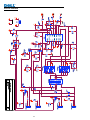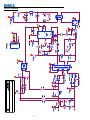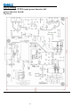
1
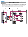
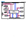
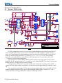
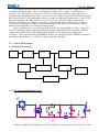
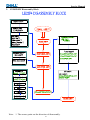
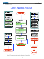
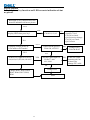
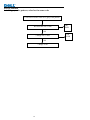
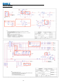
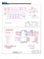
Service Manual Service Manual LCD Monitor E2209Wf 0 1 Service Manual Versions and Revision No. Version Release Date Revision 1 1.0 2008-6-3 Initial Release Copyright Copyright 2007 InnoLux Display. Corp. Ltd All Rights Reserved This manual may not, in whole or in part, be copied, Photocopied, reproduced, translated, or converted to any electronic or machine readable form without prior written permission of Foxconn Tech. Corp. Ltd. Dell E2209W Service Manual Service Manual Table of Contents CHAPTER 1- PRECAUTIONS & SAFETY NOTICES ...................................................................................................................... 3 1. 2. 3. SAFETY PRECAUTIONS...................................................................................................................................................... 3 PRODUCT SAFETY NOTICE ............................................................................................................................................... 3 SERVICE NOTES ................................................................................................................................................................... 3 CHAPTER 2- SERVICE TOOLS & EQUIPMENT REQUIRED....................................................................................................... 4 CHAPTER 3- CIRCUIT THEORY ........................................................................................................................................................ 5 1. 2. 3. 4. 5. 6. 7. 8. BLOCK DIAGRAM ..................................................................................................................................................................... 5 ELECTRONIC CIRCUIT THEORY ................................................................................................................................................ 7 FACTORY PRESET TIMING TABLE ................................................................................................................................. 13 POWER ON/OFF SEQUENCY ................................................................................................................................................... 13 D-SUB CONNECTOR PIN ASSIGNMENT .................................................................................................................................. 14 AC OUTLET PIN ASSIGNMENT ............................................................................................................................................... 14 INNER CONNECTOR PIN ASSIGNMENT .................................................................................................................................... 14 KEY PARTS PIN ASSIGNMENTS ............................................................................................................................................... 16 CHAPTER 4- DISASSEMBLY & ASSEMBLY .................................................................................................................................. 21 1. 2. 3. EXPLODED DIAGRAM ............................................................................................................................................................. 21 E2209WFPF DISASSEMBLY BLOCK ....................................................................................................................................... 22 ASSEMBLY BLOCK.................................................................................................................................................................. 23 CHAPTER 5- TEST AND ADJUSTMENT ......................................................................................................................................... 24 1. 2. 3. 4. 5. 6. 7. FUNCTION KEY DEFINITIONS .................................................................................................................................................. 24 OSD CONTROL....................................................................................................................................................................... 24 FACTORY MODE INTRODUCTION ............................................................................................................................................ 26 BURN-IN PATTERN .................................................................................................................................................................. 27 AUTO COLOR BALANCE (AUTOMATICALLY CALIBRATE CHIP ADC PARAMETER BY USING CHIP INTERNAL DAC.) ................ 27 UPLOAD FIRMWARE TO MCU VIA VGA CABLE...................................................................................................................... 26 AFTER REPAIR, TO ENSURE THE QUALITY YOU SHOULD DO THE FOLLOWING TEST AND ADJUSTMENT. ................................... 27 CHAPTER 6- TROUBLE SHOOTING ............................................................................................................................................... 30 1. 2. 3. 4. 5. 6. COMMON ACKNOWLEDGE...................................................................................................................................................... 30 NO POWER LED OFF.............................................................................................................................................................. 30 POWER NORMAL LED AMBER ................................................................................................................................................ 31 BACKLIGHT CAN’T BE TURNED ON ......................................................................................................................................... 32 NO PICTURE BACKLIGHT ON ................................................................................................................................................ 33 AT 32-GRAY SCALE PATTERN, COLOR LOST IN SOME SCALE .................................................................................................... 34 CHAPTER 7- RECOMMENDED PART LIST................................................................................................................................... 35 ATTACHMENT 1- BILL OF MATERIAL .......................................................................................................................................... 37 ATTACHMENT 2- SCHEMATIC ........................................................................................................................................................ 47 ATTACHMENT 3- PCB LAYOUT....................................................................................................................................................... 60 2 Service Manual Chapter 1- PRECAUTIONS & SAFETY NOTICES SAFETY PRECAUTIONS This monitor is manufactured and tested on a ground principle that a user’s safety comes first. However, improper used or installation may cause damage to the monitor as well as to the user. WARNINGS: This monitor should be operated only at the correct power sources indicated on the rating label on the rear cover of the monitor. If you’re unsure the power supply in your residence, consult your local dealer or Power Company. Use only the specified power cord that comes with this monitor. Do not try to repair the monitor by yourself, as it contains no user-serviceable parts. This monitor should only be repaired by a qualified technician. Do not remove the monitor cabinet. There is high-voltage parts inside that may cause electric shock to human bodies. Stop using the monitor if the cabinet is damaged. Have it checked by a service technician. Put your monitor only in a lean, cool, dry environment. If it gets wet, unplug the power cable immediately and consult your closed dealer. Always unplug the monitor before cleaning it. Clean the cabinet with a clean, dry cloth. Apply non-ammonia based cleaner onto the cloth, not directly onto the class screen. Do not place heavy objects on the monitor or power cord. PRODUCT SAFETY NOTICE Many electrical and mechanical parts in this chassis have special safety visual inspections and the protection afforded by them cannot necessarily be obtained by using replacement components rated for higher voltage, wattage, etc. Before replacing any of these components read the parts list in this manual carefully. The use of substitute replacement parts, which do not have the same safety characteristics as specified in the parts list, may create shock, fire, or other hazards. SERVICE NOTES When replacing parts on circuit boards, clamp the solder wires around terminals before soldering. Keep wires away from high voltage, high temperature components and sharp edges. Keep wires in their original position so as to reduce interference. Adjustment of this product please refers to the user’ manual. Use Pb free solder wire for circuit board preparation. 3 Service Manual Chapter 2- SERVICE TOOLS & EQUIPMENT REQUIRED 1. 2. 3. 4. 5. 6. 7. 8. 9. SIGNAL GENERATOR MULTIMETER SCREW DRIVER OSCILLOSCOPE Soldering IRON SOLDER (Lead free, RoHS compliance) Color Analyzer Fox_VISP_Programmer Fox_VEDID_Programmer 4 Service Manual Chapter 3- CIRCUIT THEORY Block Diagram There are 3pcs PCBA in this monitor, one is power& inverter&Audio board which is a single layer board, one is interface board including USB HUB 1up/2down, one is keypad which is OSD control, and one is USB transfer board located on the right side back cover. The system function block diagram as below This PWA is included switching power supplier, inverter for CCFL and interface board.(fig.1) INVERTER POWER Fig.1 5 Service Manual Fig.12 6 Service Manual Electronic Circuit Theory 2.1 Inverter PWM circuit 2.1.1)Inverter Control circuit:(fig.2) Fig.2 27VDC provides the power for U1; the control signals Brightness and ON/OFF come from I/F board. ON/OFF signal connect to pin16 of U1 and makes U1 enable. Brightness signal connect to pin12 of U1 and regulates the panel brightness, make up a network of delaying time circuit and R23 make up a divided voltage network, C3 is used to control start-up timing. The operation frequency is determined by the external Resistor R16 and capacitor C8 connected to pin3 of U1. C7 is used for soft start and compensation. The output drives, include DRV1, DRV2 (pins8,9 respectively) output square pulses to drive MOSFET Q6, Q7 and each of Q6, Q7 is consist of a N+P channel MOSFET. Q6 and Q7 work as All Bridge structure, it is high efficient, PWM switching. During start up, VSEN (pin1) senses the voltage at the transformer secondary. When VSEN reaches 3.0V, the output voltage is regulated. If no current is sensed approximately 2seconds U1 shut off. The current flowing through CCFL is sensed and regulated through sense resistor R6, R19. The feedback voltage connected to Pin1 (ISEN), then compared with a reference voltage (1.5V) via a current amplifier, resulting in PWM drive outputs to All Bridge switches. 2.1.2)Protection Circuit 7 Service Manual Over Voltage Protection and over-current protection are monitored by the voltage on VSEN(Pin 1) During normal operation , if a CCFL is damaged or removed ,the voltage at VSEN (Pin1) increases .Once the voltage at VSEN exceeds 3.0V (OVPT Setting) the driver output duty cycle is regulated and the shutdown delay timer is activated. OVPT set the overall protection threshold voltage that is lower than 3V (VSEN threshold). Once the voltage at TIMER pin reached about 3v ,the IC will shut down and latch . R3, R4,R14,R15,C1,C15,C16,C17 are connected in high voltage output connector, the divided AC voltage is inverted DC voltage through D2, D3, R9 and C11 are used to rectify wave & dump noise. Then the voltage signal reaches Pin1 VSEN of U1, when the voltage changes, build-in PWM of U1 will adjust output voltage. Open Lamp Protection: In normal operation, R10,R11 are sensed a high level DC voltage,If a CCFL is removed or damaged during normal ,the voltage at SSTCMP(Pin2) rises rapidly .when the voltage at SSTCMP reaches a threshold of approximately 2.0V,a current source charges the capacitor(C3 and C18)connected to TIMER(Pin12).Once the voltage level at the TIMER pin reaches a threshold of approximately 3.3v,The drive outputs shut down and latch . 2.2 Power PWM circuit 2.2.1) Block diagram:(fig.4) EMI Filter Rectifier and filter PWM controller Isolation power transformer Rectifier and filter Switching element Inverter circuit Rectifier and filter Interface circuit Feedback Isolation 2.2.2) AC Input and EMI Filter:(fig.5) fig.5 CN850 is a connector for connecting AC Power. F850 is a fuse to protect all the circuit AC. Input 8 Service Manual voltage is from 90V to 264V. R850/R851/R852 are joined between two inputting main circuit to prevent man from shock. L850 is used to filter low frequency noise. C850 and C851 are used to discharge the noise that L850 produced. High frequency waves are damped by C852; 2.2.3)High Voltage to Low Voltage Control Circuit:(fig.6) fig.6 D850 is a rectifier in which there are 4 build-in diodes, inverting AC to DC. C854 is used to smooth the wave from rectifier. U850 is a highly integrated PWM controller. Typical start-up current for U850 is only 20 uA, When current flow through R841/R842/R843 gets to Pin 3of U850, with VDD hold-up capacitor C855, U850 is enough for starting up. When U850 begins to operate Pin8 of U850 will output square wave to drive Q850, then the main current flow get to GND bypassing through T850, Q850. Because of the change of current flow, wires in the other side of T850 will induct current. In the same time, the current inducted by wires which connected T850 Pin 1 and Pin 3, with components of D852, R856and C855 ,will be supplied to U850 for normal operating. 9 Service Manual When the sense voltage across the sense resistor R859, reaches the threshold voltage around 0.85v, the output GATE drive will be turned off. Every time when the output of power supply is shorted or over loaded, the FB voltage will increase, the build-in PWM output will then be turned off. Both of two will prevent the power supply from being overheated under over loading condition. The PWM duty cycle is determined by this current sense signal and VFB, the feedback voltage, when the voltage on sense pin reaches V-(PWMcopm) =(Vcomp-2VF)/3, A switch cycle will be terminated immediately, Vcomp is internally clamped to a variable voltage around 0. 85 V for output power limit When Q850 are turned off, the main current flow will be consumed through D851, C875, R853/R854/R855 and D853, This will prevent Q850 from being damaged under large current impulse and voltage spike. 2.2.4)DC_27V and 5V Output Circuit and Feedback circuit:(fig.7) fig.7 D854/D855 is used to rectify the inducted current. C862 is used to store energy when current is reversed. The parts including C863 are used to smooth the current waves that are from D854/D855, then 27V voltage is supplied; D860 is used to rectify the inducted current. R861 and C873 are used to store energy when current is reversed. The parts including C866, C867, C868, and L854 are used to smooth the current waves that are from D860, then 5Vvoltage is supplied; 27V and 5V supply voltage feed back to PWM controller U850 via R871, R872, R868 and I850,I851.R860,C859 and C871 used to control respond time. 10 Service Manual 2.3 I/F Board Circuit (see the Attachment 2- Schematic) 2.3.1 RGB CAPTURE - Signal RED,GREEN,BLUE input through CN102 #1,#2,#3, Stop DC via C113, C114 and C115, and then enter into U105 (TSUMU58EHJ-LF-2) analog input PIN #28,#25,#23, and then TSUMU58EHJ-LF-2 deals with signal internally. D103, D104, D105 are ESD protector to prevent U105 from ESD. - Signal DDC_SCL (series clock) inputs via CN102#15, and then passes through ZD106 for ESD protection, goes into EDID EEPROM IC U103 #6. - Signal DDC_SDA (series data) inputs via CN102#12, and then passes through ZD103 for ESD protection, goes into EDID EEPROM IC U103 #5. - Signal TTL vertical sync. (Vsync) inputs via CN102 #14, and then clamped by ZD105 Zener, passes through R134, and then goes into IC U105 (TSUMU58EHJ-LF-2) #33. - Signal TTL horizontal sync. (Hsync) inputs via CN101 #13, and then clamped by ZD102 Zener, passes through R133, and then goes into IC U105 (TSUMU58EHJ-LF-2) #32. - CN101#5 is defined as cable detect pin, this detector realize via R121 and U104#36, and D102 is ESD protector. - U103 +5V is supplied by PC via CN102#9 with ZD102 for ESD protection, or supplied by Monitor self via D106 - U103 is an EEPROM IC which is memory and EDID data saved in it. 2.3.2 DVI CAPTURE - Differential Signal input RX0+,RX0-,RX1+,RX1-,RX2+,RX2-,RXC+,RXC- through CN201 #18,#17,#10,#9,#2,#1,#23,#24 via R206,R205,R204,R203,R202,R201,R207,R208 enter into U105 (TSUMU58EHJ-LF-2) Digital input terminal #16,#15,#13,#12,#10,#9,#18,#19, and then TSUMU58EHJ-LF-2 deals with signal internally. D206, D207, D204, D205, D202, D203, D208, D209 are ESD protector to prevent U105 from ESD - Signal DDC_SCL (series clock) inputs via CN201#6, and then passes through ZD204 Zener for ESD protection, via R209, goes into EDID EEPROM IC U201 #6. - Signal DDC_SDA (series data) inputs via CN201#7, and then passes through ZD203 Zener for ESD protection, via R210, goes into EDID EEPROM IC U201 #5. - CN201#15 is defined as cable detect pin, this detector realize passes through R216 ,go into U105#49, and D210 is ESD protector. - U201 +5V is supplied by PC via CN201#14 through D201, or supplied by Monitor self via D201. - U201 is an EEPROM IC which is memory and DVI input EDID data saved in it. 2.3.3 Buttons Control - Button “Power” on front bezel connects to U105 (TSUMU58EHJ-LF-2) #4 through CN104 #8, U105 #4 is defined as power on/off. - Button “+” on front bezel connects to U105 (TSUMU58EHJ-LF-2) #120 through CN104 #2, U105#120 Voltage is defined as “Plus”. - Button “-” on front bezel connects to U105 (TSUMU58EHJ-LF-2) #121 through CN104 #3, U105 #121 Voltage is defined as “Minus”. - Button “Menu” on front bezel connects to U105 (TSUMU58EHJ-LF-2) #50 through CN104 #1, U105 #50 Voltage is defined as “Menu”. - Button “SELECT” on front bezel connects to U105 (TSUMU58EHJ-LF-2) #122 through CN104 #4, U105 #122 Voltage is defined as “SELECT”. - LED Indicator on Front Bezel a. When press button “power”, U105 (TSUMU58EHJ-LF-2) #123 be send in low Voltage, make Q107#3 sends out high Voltage , and then to CN01#5 on keypad, LED green on. b. When in “Suspend” mode, U105 (TSUMU58EHJ-LF-2) #124 sends out a low Voltage, make Q108#3 sends out high Voltage and then to CN01 #7 on keypad, LED Amber ON. 2.3.4 MATAR CHIP U105 (TSUMU58EHJ-LF-2) - U105 (TSUMU58EHJ-LF-2) #91~#100 output 8 bit even and #77~#86 output 8 bit odd LVDS digital data to panel control circuit through CN103. 11 Service Manual - U105 (TSUMU58EHJ-LF-2) #73 output PPWR ”H” potential to make Q104 conducted, and then make Q101 conducted, +5V flow to CN103#1~#3 as Panel Vdd . - U105 (TSUMU58EHJ-LF-2) #109 output CCFL_ON/OFF ”L” potential to control Inverter on/off. - U105 (TSUMU58EHJ-LF-2) #125 outputs Brightness “PWM” signals to control CCFL brightness. - TCLK by Crystal 14.318MHz input to U105 (TSUMU58EHJ-LF-2) #128/#127. - U105 (TSUMU58EHJ-LF-2)#108 is RESET signals input pin Please refer to U105 (TSUMU58EHJ-LF-2) Pin Assignments table in page 2.3.5 Regulator Circuit - +3.3V is generated from Regulator U101 which is supplied by+5V via R101 and through C104 filtering, -+1.8V is generated from Regulator U102 which is supplied by+3.3V through C106 filtering, 3. FACTORY PRESET TIMING TABLE Standard VESA IBM DOS Resolution 720 x 400 640 x 480 640 x 480 800 x 600 800 x 600 1024 x 768 1024 x 768 1152 x 864 1280 x 1024 1280 x 1024 1680 x 1050 720 x 400 Horizontal Frequency (KHz) 31.469 31.469 37.500 37.879 46.875 48.363 60.023 67.500 64.000 79.976 65.160 31.469 Vertical Frequency (Hz) 70.087 59.940 75.000 60.317 75.000 60.004 75.029 75.000 60.000 75.025 60.0 70.087 4. Power On/Off Sequency Hardware power On/Off When power cord plug into AC socket, Power provides 26V and DC_5V. DC_5V is main voltage for panel and Regulator U101. DC_3.3V is coming from Regulator U101, DC_3.3v is main voltage for U105. When DC_3.3V input to U105 and U105 reset circuit active, U105 all registers will be set to default, that means finish hardware power on. When pull out power cord from AC socket,the system shut down instantly for no supply Software power On/Off - When press power key, U105 #4 receives low pulse, then U105 (TSUMU58EHJ-LF-2) will be wake up and send control signals(at 73,109pin) to on CCFL and switch 5.0v to panel module, at the same time,U105 make the VGA/DVI cable input signal source display normal on panel if the VGA/DVI cable input signal is active - If power ON, U105 #123 (LED_blue) will send out low potential, and then LED blue on. - If power saveing, U105 #124 (LED_Amber) will send out low potential, and then LED Amber on. - If power ON or power saveing, when press power key, U105 #4 receives low pulse, then U105 will be sleeping and turn off backlight, at the same time, the panel will lose +5V. The Panel_Vcc, Backlight_En, CLK/DATA output to panel will follow the following sequency. 12 Service Manual Power supply for panel+5V VDD 90% 90% 10% 0V 10% T1 T2 T5 Signals (Digital RGB, HS, VS, DE, CLOCK) 0V T6 T7 Valid data T3 T4 Power supply for backlight SPEC(Samsung) SPEC (INL) T1(ms) 0.3~10 0.1~10 T2 (ms) 0.0~50 0.0~50 T3 (ms) >500 >200 T4 (ms) >100 >100 T5 (ms) 0.0~50 0.0~50 T6 (ms) NA >0.1 T7(ms) >1000 >1000 5. D-SUB Connector Pin Assignment Pin 1 2 3 4 5 Symbol Red Green Blue GND Cable Detect Pin 6 7 8 9 10 Symbol Red_GND Green_GND Blue_GND PC+5V GND 6. AC Outlet Pin Assignment Pin 1 2 3 Symbol Line GND Neutral 7. Inner Connector Pin Assignment 7.1 CN103 (Connect M/B to Panel,) Pin Symbol 1 Panel_Vcc 2 Panel_Vcc 3 Panel_Vcc 4 NC 5 NC 6 NC Description Panel power supply (typ.5.0V) Panel power supply (typ. 5.0V) Panel power supply (typ. 5.0V) 13 Pin 11 12 13 14 15 Symbol GND DDC_SDA Hsync Vsync DDC_SCL Service Manual 7 8 9 10 11 12 13 14 15 16 17 18 19 20 21 22 23 24 25 26 27 28 29 30 GND_LVDS RXE3+ RXE3RXEC+ RXECRXE2+ RXE2GND_LVDS RXE1+ RXE1GND_LVDS RXE0+ RXE0RXO3+ RXO3RXOC+ RXOCGND_LVDS RXO2+ RXO2RXO1+ RXO1RXO0+ RXO0- LVDS Ground LVDS signal of even channel 3(-) LVDS signal of even channel 3(+) LVDS signal of even channel clock (+) LVDS signal of even channel clock (-) LVDS signal of even channel 2(+) LVDS signal of even channel 2(-) LVDS Ground LVDS signal of even channel 1(+) LVDS signal of even channel 1(-) LVDS Ground LVDS signal of odd channel 0(+) LVDS signal of odd channel 0(-) LVDS signal of odd channel 3(+) LVDS signal of odd channel 3(-) LVDS signal of even channel clock (+) LVDS signal of even channel clock (-) LVDS Ground LVDS signal of even channel 2(+) LVDS signal of even channel 2(-) LVDS signal of even channel 1(+) LVDS signal of even channel 1(-) LVDS signal of odd channel 0(+) LVDS signal of odd channel 0(-) 7.2 CN1, CN2, CN3, CN4 (Connect to Panel Backlight,) Pin Symbol 1 HV High voltage for lamp 2 LV Low voltage for lamp Description 7.3 CN104 (Connect to keypad, WAFER2*4P or compatible connector) Pin Symbol Description 1 MENU OSD “MENU” control 2 PLUS OSD “+” control and “Brightness/Contrast” adjustable hot key 3 MINUS OSD “-” control and “Auto adjust” adjustable hot key 4 SELECT OSD “input source Select” control 5 LED Blue LED Blue on/off control 6 GND Ground 7 LED Amber LED amber on/off control 8 POWER Ground 14 Service Manual 8. Key Parts Pin Assignments U105(TSUMU58EHJ-LF-2) 15 Service Manual 16 Service Manual 17 Service Manual 8.1 U108 (Serial Flash) Pin Symbol I/O 1 CE# I 2 3 SO WP# I/O I/O 4 5 VSS SI G I/O 6 SCK I/O 7 HOLD I/O 8 VDD P Description The device is enabled by a high to low transition on CE#. CE# must remain low for the duration of any command sequence. To transfer commands, addresses, or data serially into the device. The write protect (WP#) pin is used to enable/disable BPL bit in the status register. Connect ground To transfer commands, addresses, or data serially into the device input are latched on the rising edge of the serial clock. To provide the timing of serial interface. Commands, addresses, or input data are latched on the rising edge of the clock input, while output data is shifted out on the Falling edge of the clock input. To temporarily stop serial communication with SPI flash memory without resetting the device. To provide power supply. 18 Service Manual 8.3 U850 (LD7552B, PWM Power Controller) Pin Symbol I/O Description 1 GND Ground 2 COMP I Voltage feedback pin(same as the COMP pin in UC384X).By connecting a photo-coupler to close the control loop and achieve the regulation. 3 VCC I Supply voltage pin 4 RT I This pin is to program the switching frequency. By connecting a resistor to ground to set the switching frequency. 5 NC Unconnected pin 6 CS I Unconnected pin 7 VCC I Supply voltage pin 8 OUT O Gate drive output to drive the external MOSFET 8.4 U1 (INL833, CCFL Inverter controller IC) Pin Symbol I/O Description 1 I VSEN Voltage sense Feedback 2 I SSTCMP Capacitor for soft-star and loop compensation 3 I CT Timing resistor and capacitor for operation and striking frequency 4 I RT1 Timing resistor for striking frequency 5 GNDA Signal Ground 6 O PDR2 High side Driver output2 7 GNDP Power Ground 8 O NDR2 Low side Driver output2 O 9 NDR1 Low side Driver output1 O 10 PDR1 High side Driver output1 I 11 VDDA Input power Pin I 12 TIMER Timing capacitor for Delay Timer I 13 PWM External PWM Dimming Input I 14 ISEN Current sense feedback I 15 OVPT Over-voltage protection threshold voltage I 16 ENA IC Enable/Disable 19 Service Manual Chapter 4- Disassembly & Assembly 1. Exploded Diagram 20 Service Manual 2. E2209WFPf Disassembly Block Note: 1. The arrows point out the direction of disassembly. 21 Service Manual 3. Assembly Block Note: 1. The arrows point out the direction of assembly 22 Service Manual Chapter 5- TEST AND ADJUSTMENT 1. Function key Definitions Menu Enter Power Power Switch with power LED indicator Power: On/Off, includes power indicator and Power ICON green- Active On Front Panel Controls Amber- DPMS 1- Input select: Select input signal 2- Menu: Call out OSD Menu and choose 3- (): symbol molded into button, calls out brightness/Contrast, move down the highlight bar. 4-()symbol molded into button, move up the highlight bar Hot Key Function Automatic adjust: Directly press “” Factory Modes Keys Function Brightness/Contrast Icon: Directly press “” Auto Color Balance Purpose: Automatically calibrate chip ADC parameter by using chip internal DAC. Process: If we want to do “Auto Color Balance” again, please confirm the following steps. 1) Connect the VGA cable with the standard video pattern generator and display the pattern with blackest and whitest colors. 2) Press “Power Key”, to power off the monitor. 3) Press “Menu Key” and “Up Key” simultaneously, and then press “Power Key” to power on the monitor. 4) Press “Plus Key”, choose “Auto color” at bottom 5) Then execute Auto Color item. 6) After the “Auto Color Balance” process finished, go back to the submenu of “Other Settings”, and press “Factory Reset” to exit 23 Service Manual Factory mode. OSD Control 1st Level 2nd Level Auto Adjust(For VGA) Input Source 3rd Level Brightness Contrast Press √to adjust the screen automatically Auto Select VGA DVI-D Input Color Format Mode Selection Preset Modes 4th Level RGB Graphics Standard MultiMedia Game Warm Cool Custom(R,G,B) Color Settings 5th Level YPbPr Video R G B Reset Color Settings Horizontal Position Vertical Position Sharpness Pixel Clock Phase Reset Display Settings English Español Français Deutsch Português (Brasil) 简体中文 日本語 Language Other Settings Menu Transparency Menu Timer Menu Lock Lock DDC/CI Enable LCD Conditioning Factory Reset(Reset All settings) Enable 24 Unlock Disable Disable Service Manual Factory Mode Introduction With signal input, press “Power” button to turn off the monitor. Press “Menu” and “Auto/Plus” buttons together, and then press “Power” button to turn on the monitor. After power on.Press “Plus Key”, enter Factory mode (Fig.10). Fig9 Fig10 Back: Exit from Factory mode and back to NO OSD Status. Panel: The current-setting panel is highlighted. Auto Color: Automatically calibrate chip ADC parameters by using internal DAC. 25 Service Manual Burn In: Enable or disable the Burn-in mode by choosing ON or OFF. Reset Timer: Reset the “Turn-on time” of the panel to 0H0M. Color Temp: The R, G, B of Blue Preset (9300K), Red Preset (5700K) and Normal Preset (6500K) are generated from scaling chip’s back-end white-balance program. Time: Turn-on time of the panel. DEBUG: Debug tool of scale IC U104. Dell panel P/N LCD supplier Samsung INL CMO Panel Supplier P/N Dell P/N 22”W 22”W 22”W LTM220M1-L01 MT220WW01-V0 M220Z1-L03 MY228 D569C P546G Burn-in pattern Burn-in pattern will self-generate automatically without VGA and DVI cable plugged in when the monitor set at Burn-in on mode and burn-in pattern will not be stopped until plugging in the VGA cable. Exit Burn-in mode method as followe: plugging in the VGA/DVI cable, press “Menu” button to call out OSD Main Menu, Press “Plus Key”to select“Other Settings Menu”then pop submenu and choose Factory reset. Auto Color Balance (Automatically calibrate chip ADC parameter by using chip internal DAC.) 5.1 If it is a new-built set, press “Auto/Plus” button to execute “Auto Color” at standard video pattern 5-MOSAIC pattern 5.2 Please confirm the following steps to perform “Auto Color Balance”: - Connect the VGA cable with the standard video pattern generator and display 5-MOSAIC pattern on the monitor. - Press “Power” button to power off the monitor. - Press “Menu” and “Auto/Plus” buttons simultaneously; then press “Power” button to power on the monitor. - Press “Plus Key”, select“Other Settings Menu” ,then Press “Plus Key”and choose factory at bottom - Set BurnIn Mode item to ON, then execute Auto Color item. - After the “Auto Color Balance” process finished, go back to “Other Settings Menu”, and press “Factory Reset” to exit Factory mode Upgrade Firmware to Serial via Flash Cable by ISP_Tool V4.100.exe 7.1 Connect the monitor and PC follow Fig 11 26 Service Manual Fig 11 ※ The detailed reprogramming procedures will be described in ISP User's Guide. After repair, to ensure the quality you should do the following test and adjustment. 27 Service Manual Item Test OSD function Content Equipment 1.Signal is set as 1680×1050@60Hz under General-1 Chroma Signal Generator 2. LCM button are from left to right, checking whether each single function key and compound function key can be worked. Contrast Check 1. Set input mode to 1680×1050@60Hz 2. Set to 32gray scale pattern 3. Set contrast to the maximum. At most 6 bars cannot be distinguished. 1. Do “Auto color Balance” at 1680×1050@60Hz, 32gray scale pattern 2. Measure color temperature, check if it complies with the following temperature : Warm x=0.328 +/- 0.03, y=0.344+/-0.03 Desktop x= 0.313 +/- 0.03, y=0.329+/-0.03 Cool x= 0.283 +/- 0.03, y=0.298+/-0.03 1. Use Chroma Pattern Generator to make sequence. VESA (640x480 800x600 1024x768 1152x864 1280x1024 1680×1050@60Hz ), the detail supported modes (see table 1) and power saving signal. 2. Confirm the above timing modes must be full screen and the picture must be normal. 3. LED is amber at power saving mode. Chroma Signal Generator VGA cable detector Y measurement at default setting When select VGA model and VGA cable is not plugged out, self-test OSD will be floated. 1. Set brightness and contrast to default value 75 at 6500K 2. With full white pattern, Y shall be 220 20 cd/m2 Visual check OSD Lock Test Soft Lock: When OSD is locked, this icon should appear for only 2 seconds with all buttons pressed, except for the “Menu” and “Power” ones. Hard Lock: Press “Menu” button for 15 seconds enables the “locked” icon to be displayed, which will lock All buttons expect for the “Power”. Press “Menu” button for another 15 seconds enables the “unlock” icon to be shown. 1. Mode:1680×1050@60Hz 2. Set Brightness& Contrast to default value (75%) 3. Do “Auto Adjustment” 4. Shut down PC to check whether there’s flicker on the center of the picture. 1. Mode:1680×1050@60Hz 2. Pattern: full Black 3. Brightness: Max. 4. Contrast: Default 5. Check power consumption at each modes State Power Consumption LED color Normal(with full <46W blue load) <2W Stand By amber Power Key Off <1W no Color Temperature Modes switching check Panel Flicker check Power saving 28 Chroma Signal Generator and color analyzer Chroma Signal Generator Chroma Signal Generator and Color Analyzer Visual Inspection Equipment:: Chroma Signal Generator & PC Chroma signal generator and Power meter AC input:230V/50Hz Service Manual Chapter 6- TROUBLE SHOOTING Common Acknowledge If you change the M/B, be sure that the U101,U102 and U105 these three components also changed to the new M/B because there was program inside. If not, please re-write EDID or upload firmware into serial flash(U105) via VGA Cable. How to do please refer to the Page 19. If you adjust clock and phase, please do it at condition of Windows shut down pattern. Please confirm the R/G/B color under 32gray scale pattern. This LCM is analog interface. So if the entire screen is an abnormal color that means the problem happen in the analog circuit part, if only some scale appears abnormal color that stand the problem happen in the digital circuit part. If you check the H/V position, please use the crosshatch pattern. This LCM support 10 timing modes, if the input timing mode is out of specification, “Cannot Display this Video Mode” will be displayed on the screen. If brightness uneven, repairs Inverter circuit or change a new panel. If you find the vertical line or horizontal line lost on the screen, please change panel. If the self-test pattern is moving on the screen, please check whether VGA Cable is plugged in the Monitor or PC if select analog model on OSD or check whether DVI Cable is plugged in the Monitor or PC if select DVI model on OSD . If the VGA or DVI Cable is plugged in well, please change another VGA or DVI cable. No Power and LED Off Is there DC24V output Is there DC5V at L854; NO Is the voltage at C854 in the range of 127V~339V? YES NO Check RT850, F850 Is the voltage at pin4 of U850 312V? YES NO Check F850 Is the voltage at pin6 of U850 0.9V? YES NO Check D852, D851 Is the voltage at pin6 of T850 120V? YES Check Q850 29 Service Manual Power(include IF +5Vand +3.3V) supply normal but LED off and no display Is the key function OK? Yes Press power key to DC on the monitor, if display ok the process is end, if no display see the no backlight process NO NO Is the frequency 14.318MHz at #127,#128 of IF Board U105? Yes Change crystal X101 NO Is the low active reset signal at #108 of IF Board U105 normal? NO Yes Yes Change C164 Change U104 NO Is the serial clock signal at #6 of IF Board U108 normal when power AC on? Change U108 Yes Upgrade Firmware to Serial Flash U108 by VGA port with ISP_ Tool V4.100.exe END Power(include IF +5Vand +3.3V) supply and display normal only LED off NO Is the keypad cable connective OK Reassembly or changing Yes NO Is LED at keypad work OK Yes Is R165 open? yes Change LED Change R165 NO Is Q107 work normal? NO Change Q107 Yes Is theLED control signal at 123# of U105 high-low convertible when DC on/off END 30 NO Change U105 Service Manual Power (include IF +5Vand +3.3V) supply and display normal but LED Amber Is Power LED Amber? YES Do the Hsync. & Vsync. Signals exist in CN102 #13& #14 separately when select VGA mode by OSD? NO Insert VGA Cable correctly YES Do the Hsync. & Vsync. Signals exist in R133 & R134? NO Check R133 & R134 YES Do the Hsync. & Vsync. Signals exist in U105#32& #33? NO Change R135 & R136 YES Is the Q108 work normal NO Change Q108 YES Is theLED control signal at 4# of U105 high-low convertible when DC on/off END 31 NO Change U105 Service Manual 4.Power (include IF +5Vand +3.3V) supply normal ,key function OK,but backlight can’t be turned on No backlight Yes LED lamp is OK No No power supply to inverter Yes Check the cable that from I/F BD to P/I BD is ok Yes No Is there 27V Voltage on Pin 7,8 & 13,14 of T1 Q6, Q7 fail Yes No Is there PWM signal on Pin13 of U1 No Check power supply Yes Replace Q6, Q7 Check I/F BD Yes No Is there High level voltage on Pin16 of U1 Check I/F BD Yes Yes Vsense voltage is 2.9V Lamp connector opened No No Are there PWM signal on pint on Pin12 of U1 U1 Failure Yes Pin14 of U1 Voltage is Low Level Pin6&10 of U1 voltage is high level voltage Yes Yes Feedback circuit failure U1 protected Yes END 32 Yes Yes Check R21,R22,C10 Check ZD1, R1 , ZD2, R2, C12, C13 Service Manual 5. Backlight on, key function and LED accurate indication ok but no picture Backlight on ,key function and LED accurate indication ok but no picture YES YES IS the display is white and cannot display OSD when press key? Check DC 5.0V on CN103#1, #2, #3 NO Is the panel enable signal at 73# of U105,if no check Q104 circuit or change U105,if yes Check Q101 circuit NO VGA Is display selftest picture at VGA mode or DVI mode? DVI Is there RGB signal in U104 #28, #25 #23? NO Change D103, D104 & D105 YES Is the FFC cable inserting ok,if no reinsert else change FFC cable Yes YES Is there DVI signal in U105 #9, #10,#12,#13,#15,#16,#18 #19? Are there data output on U105#77~#86 #91~#100 No Change U105 Change D202, D203, D204, D205, D206, D207, D208, D209 END 33 Service Manual 6.At 32-gray scale pattern, color lost in some scale Color lost in some scale at 32-gray scale pattern Re-insert the FFC Cable OK, END NO Change FFC Cable NO Change U105 34 OK, END Service Manual Chapter 7- RECOMMENDED PART LIST Content PI BD IF BD PN Description 412000628810R IC LD7552BPS 412000654630R Supplier SOP8(Leadtrend)ROHS Usage LEADTREND, 1 IC INL833GN SOP16(O2 MICRO)Rohs O2, 1 426000091010R XFMR SW DIP ERL28 PC40 550uH SPW-101 RoH FOXCONN,FRONTIER,LISHIN,MEIKAI, 0 426000091160R XFMR SW DIP EEL22 P4 4.16H DARFON,FOXCONN,HUALON,LISHIN, 1 420431014083R CAP SEK 100uF/450V M,105℃ CF 18x40(2.5) ELITE,SAMXON,SU'SCON, 0 410500059290R XSTR AP2761I-A N-CH TO-220CFM ADVANCED P APEC 1 410050103050R XSTR FMA09N65GX FUJI 0 410050057280R XSTR STP8NK80ZFP N-CH TO220FP (ST) ST 0 491571400100H PCB,P/I HSIANGKUO,TAT CHUN, 1 412000653060R IC TSUMU58EHJ-LF-2 MSTAR 1 412000494190R IC SST25LF020A-33-4C-SAE SOIC8(SST)ROHS SST, 1 412000494310R IC PM25LV020-100SCE SOIC8(PMC)RoHS PMC, 0 412000224482R IC AT24C16BN-SH-T 16K(ATMEL) SOIC 8 ROHS ATMEL, 1 412000224280R IC M24C16-WMN6TP SO8 16K (ST) ROHS ST, 0 412000481990R IC CAT24C16WI-TE13 SOIC-8(CATALYST)RoHS CATALYST, 0 412000332020R IC LD1117AL-3.3-A TO-252(UTC)RoHS UTC, 1 412000332130R IC AP1117D33LA 3.3V (ANACHIP) TO-252-3L, ANACHIP, 0 412000332830R IC AS1117R-3.3.TR-LF,TO-252(A1 SEMI)RoHS A1SEMI, 0 412000330020R IC LD1117AL-1.8V-A SOT223(UTC) RoHS UTC, 1 412000330830R IC AS1117L-1.8/TR-LF,SOT223(A1 SEMI)RoHS A1SEMI, 0 412000330070R IC AZ1117H-1.8 SOT223(AAC)RoHS BCD, 0 412000435481R IC AT24C02BN-SH-T 2K SOIC8(ATMEL)RoHS ATMEL, 1 412000480280R IC M24C02-RMN6TP SO8(ST)RoHS ST, 0 412000480990R IC CAT24C02WI-TE13 SOIC-8(CATALYST)RoHS CATALYST, 0 SPW-116 ROHS N-CH TO-220F(FUJI) RoHS ,1/OSP /CEM1/16,LE22F4-612 35 PQFP128(MSTAR)Rohs E Service Manual ATTACHMENT 1- Bill of Material 1. Interface board BOM 2E+07 ITEM P/N 791701300B00R 10 629030018710R 20 791701320600R 30 791701340600R 40 511130001200R 50 641120000010R Description PCBA,I/F BOARD W/O SPK,LE22F4-B12 ROHS PROGRAM,W/O SPK LE22F4-B12 ROHS PCBA,I/F BOARD,MI,W/O SPK,LE22F4-612 ROH PCBA,I/F BOARD,SMT,W/O SPK,LE22F4-612 RO SOLDER BAR,Sn96.5/Ag3.0/Cu0.5/Ni0.06/Ge0 HDCP RECEIVE DEVICE KEY LABEL,BARCODE,BLANK,33x7mm, ROHS,FOR PCB Supplier 2E+07 ITEM P/N 791701320600R 10 430631080170R 20 440819015030R 30 430631080180R 40 443842024060R 50 432008010270R 60 420271010460R 70 420432200460R Description PCBA,I/F BOARD,MI,W/O SPK,LE22F4-612 ROH WFR 8P 2.0MM 180° W/LOCK ROHS CON D-SUB FEM.15P RA W/O SCREW DZ11AA1-H WFR 2X4P 2.0MM 180° W/LOCK ROHS CON DVI-D RA 24+1P FEM.W/O SCR EW QH1112 XTAL 14.31818MHz HC-49US DIP 16pF 30PPM CAP SE 100uF 16V M,105℃ ST,6.3*11 ROHS CAP EC 22uF 16V M,105℃ ST, 5x11,RoHS Supplier 2E+07 ITEM P/N 791701340600R 10 444099030040R Description PCBA,I/F BOARD,SMT,W/O SPK,LE22F4-612 RO CON, SMD 1.0MM 30PIN with lock RoHS Supplier 60 506140005700R Usage 1 1 1 2.2 1 TOMAS, DCP LLC, HENGMINGDA,JIAYINMEI,KAIDA, 1 Usage CVILUX,FOXCONN,JOWLE, CVILUX,DLK,FOXCONN,JOWLE,TEKCON,ZJGHJ, CVILUX,FOXCONN, DLK,FOXCONN,ZJGHJ, HUAN MOUN,TXC,ZGC, SAMXON,SU'SCON,TEAPO, ELITE,LELON,SAMXON,SU'SCON,TEAPO, CVILUX,P-TWO, Location Location 1 1 1 1 1 2 3 Usage CN101, CN102, CN104, CN201, X101, C109,C102, C103,C142,C150, Location 1 CN103, C106,C108,C110,C126,C128,C133,C134,C135,C136, C137,C138,C139,C140,C141,C143,C144,C145,C146, C147,C149,C153,C154,C155,C156,C159,C160,C161, 53 C165,C167,C168,C169,C170,C171,C172,C173,C201, C202,C213,C111,C122,C123,C124,C125,C203,C204, C205,C206,C207,C208,C209,C210,C211,C212, 20 419351044010R C SMD(0402) X5R 0.1uF/16V K,RoHS DARFON,WALSIN,YAGEO, 30 419311054070R C SMD(0805) X7R 1uF/16V K RoHS REV:A DARFON,MURATA,TDK,WALSIN, 2 C112,C164, 40 50 60 70 C SMD(0402) X7R 0.047uF/16V K,RoHS C SMD(0402) NPO 27PF/50V J RoHS C SMD(0603) X5R 1uF/16V K,RoHS C SMD(0402) NPO 22PF/50V J,RoHS DARFON,WALSIN,YAGEO, DARFON,MURATA,TDK,WALSIN,YAGEO, DARFON,MURATA,SAMSUNG,TDK,WALSIN,YAGEO, DARFON,MURATA,TDK,WALSIN,YAGEO, 7 2 1 2 DIO BAV99 350mW 70V SOT-23(PHI RoHS PHILIPS, DIO BAV99 350mW 75V SOT-23(PEC RoHS DIO BAV99-LF 350mW 70V SOT-23 (FEC)RoHS DIO BAV70 85V SOT23 (PHILIPS) RoHS DIO BAV70, 70V SOT-23(PEC) ROHS DIO BAV70-LF, 70V SOT-23(FEC) ROHS BEAD CORE SMD(0603)120Ω 300mA SBK160808 BEAD CORE SMD(0603)60Ω 600mA, GBK160808 XSTR AP2305GN P-CH SOT23(APEC) RoHS XSTR AO3415 P-CH,SOT23(AOS) RoHS XSTR AM2321P-T1-PF P-CH SOT23(ANALOG POW XSTR PMBT3904 NPN 200MA,40V SOT23(PHILIP XSTR MMBT3904LT1G NPN 200MA 40V SOT23(ON XSTR MMBT3904 NPN SOT-23(PANJIT)RoHS XSTR PMBT3906 PNP 200MA,40V SOT23(PHILIP XSTR MMBT3906 PNP SOT-23(PANJIT)RoHS XSTR MMBT3906LT1G PNP 200mA 40V SOT23(ON RES SMD (1206) 0Ω J,RT RoHS REV:A RES SMD (0603) 0Ω J,RT RoHS PANJIT, FRONTIER, PHILIPS, PANJIT, FRONTIER, CHILISIN,TAI-TECH, CHILISIN,TAI-TECH, APEC, AOS, AP, PHILIPS, ON SEMI, PANJIT, PHILIPS, PANJIT, ON SEMI, TA-I,WALSIN,YAGEO, TA-I,WALSIN,YAGEO, 170 414918010350R RES SMD (0402) 10KΩ J,RT,RoHS TA-I,WALSIN,YAGEO, 180 414918000050R RES SMD (0402) 0Ω J,RT,RoHS TA-I,WALSIN,YAGEO, 190 414918047250R RES SMD (0402) 4.7KΩ J,RT,RoHS TA-I,WALSIN,YAGEO, 200 414918010450R 210 414918047350R RES SMD (0402)100KΩ J,RT,RoHS RES SMD (0402) 47KΩ J,RT,RoHS TA-I,WALSIN,YAGEO, TA-I,WALSIN,YAGEO, R105,R110,R127,R128,R137,R138,R188,R211,R212, R219, 4 R107,R109,R106,R175, 1 R108, 220 414918750910R RES SMD (0402) 75Ω F,RT,RoHS TA-I,WALSIN,YAGEO, 9 R117,R118,R119,R114,R115,R116,R122,R123,R124, 230 414918047150R RES SMD (0402) 470Ω J,RT,RoHS TA-I,WALSIN,YAGEO, 240 414918010250R RES SMD (0402) 1KΩ J,RT,RoHS TA-I,WALSIN,YAGEO, 15 250 260 270 280 RES SMD (0402) 100Ω J,RT,RoHS RES SMD (0402) 2.2KΩ J,RT,RoHS RES SMD (0402) 390Ω F,RT,RoHS RES SMD (0603) 330Ω J,RT RoHS TA-I,WALSIN,YAGEO, TA-I,WALSIN,YAGEO, TA-I,WALSIN,YAGEO, TA-I,WALSIN,YAGEO, 6 2 1 1 290 414918010050R RES SMD (0402) 10Ω J,RT,RoHS TA-I,WALSIN,YAGEO, 8 R201,R202,R203,R204,R205,R206,R207,R208, 300 300 300 300 310 310 310 310 IC AP1117D33LA 3.3V (ANACHIP) TO-252-3L, IC AME1117CCCTZ 3.3V,TO-252(AM E)RoHS IC LD1117AL-3.3-A TO-252(UTC)RoHS IC AS1117R-3.3.TR-LF,TO-252(A1 SEMI)RoHS IC LD1117AL-1.8V-A SOT223(UTC) RoHS IC AS1117L-1.8/TR-LF,SOT223(A1 SEMI)RoHS IC AZ1117H-1.8 SOT223(AAC)RoHS IC MT11171.8A SOT223(Matrix) RoHS ANACHIP, AME, UTC, A1SEMI, UTC, A1SEMI, BCD, MATRIX, 1 U101, 0 0 0 1 U102, 0 0 0 419314734010R 419302700510R 419351054060R 419302200510R 80 411020026210R 80 80 90 90 90 100 110 120 120 120 130 130 130 140 140 140 150 160 411020026090R 411020026020R 411020047210R 411020047090R 411020047020R 432002312144R 432002360140R 410500068290R 410500075270R 410060018380R 410500045210R 410500045140R 410500045090R 410500046210R 410500046090R 410500046180R 414904000050R 414916000050R 414918010150R 414918022250R 414918390010R 414916033150R 412000332130R 412000241550R 412000332020R 412000332830R 412000330020R 412000330830R 412000330070R 412000598490R 36 13 0 0 2 0 0 1 2 1 0 0 3 0 0 2 0 0 2 4 C113,C114,C115,C119,C120,C121,C152, C130,C129, C148, C157,C158, D102,D103,D104,D105,D202,D203,D204,D205,D206, D207,D208,D209,D210, D106,D201, FB101, FB102,FB105, Q101, Q104,Q201,Q103, Q107,Q108, R101,R113, RB101,RB102,RB103,R164, R102,R129,R140,R150,R151,R152,R166,R169,R171, 24 R172,R174,R176,R177,R178,R179,R180,R190,R192, R213,R217,R103,R220,R184,R161, 3 R121,R147,R148, 10 1 R159, R130,R133,R134,R145,R146,R153,R154,R155,R160 R191,R214,R125,R216,R157,R158, R131,R132,R142,R143,R209,R210, R135,R136, R144, R165, Service Manual 320 320 320 330 340 340 340 350 350 412000435481R 412000480280R 412000480990R 412000653060R 412000224482R 412000224280R 412000481990R 412000494190R 412000494310R IC AT24C02BN-SH-T 2K SOIC8(ATMEL)RoHS IC M24C02-RMN6TP SO8(ST)RoHS IC CAT24C02WI-TE13 SOIC-8(CATALYST)RoHS IC TSUMU58EHJ-LF-2 PQFP128(MSTAR)Rohs IC AT24C16BN-SH-T 16K(ATMEL) SOIC 8 ROHS IC M24C16-WMN6TP SO8 16K (ST) ROHS IC CAT24C16WI-TE13 SOIC-8(CATALYST)RoHS IC SST25LF020A-33-4C-SAE SOIC8(SST)ROHS IC PM25LV020-100SCE SOIC8(PMC)RoHS ATMEL, ST, CATALYST, MSTAR, ATMEL, ST, CATALYST, SST, PMC, 2 0 0 1 1 0 0 1 0 360 411130962950R ZENER 6.2V MMSZ5234B SOD-123(PANJIT)RoH PANJIT, 9 360 360 370 380 ZENER 6.2V BZT52-C6V2 SOD-123(WILLAS)ROH ZENER 6.2V BZT52C6V2-7-F SOD-123(DIODES) PCB I/F BOARD LE19H0 RES SMD (0603) 560Ω J,RT RoHS REV:A WILLAS, DIODES, TIP TOP,WELFARE, TA-I,WALSIN,YAGEO, 0 0 1 1 R168, 411121462950R 411131562950R 491351300100H 414916056150R U103,U201, U105, U106, U108, ZD102,ZD103,ZD104,ZD105,ZD106,ZD201, ZD203,ZD204,ZD107, 2. power board BOM ITEM P/N Description Supplier Usage Location 791701400600R PCBA,P/I BOARD W/O SPK,LE22F4-612 ROHS 10 430637020030R WFR. 2P P=3.5mm 90°W/LOCK,RoHS CVILUX,FCN,FOXCONN, 4 CN1,CN2,CN3,CN4, 20 440149000350R SKT AC 10A/250V U/C/V, H 1.0MM ROHS TECX, 1 CN850, HRN ASS'Y 8P 130mm UL1007 30 430300801650R ROHS FOXCONN,HEIGHTEN,JVE, 1 CN853, 40 420424710510R CAP SD 470uF/50V M 105℃ F 13x21 RoHS LELON,SAMXON,SU'SCON,TEAPO, 2 C20,C863, 50 418103051920R CAP CD NPO 3pF 3KV D,S7.5, RoHS JNC,SUCCESS(SEC), 4 C21,C22,C23,C24, 50 418103058920R CAP CD SL 3pF 3KV D,S7.5,RoHS JNC,SUCCESS(SEC), 0 60 418105051920R CAP CD NPO 5pF 3KV D,S7.5, RoHS JNC,SUCCESS(SEC), 2 C25,C27, JNC,POE,SUCCESS(SEC),TDK, 2 C850,C851, JNC,POE,SUCCESS(SEC), 0 80 416194743011R CAP MEX 0.47uF 275V K X2,F15 RoHS ARCOTRONIC,EUROPTRONIC,HJC,SCC, 1 C852, 90 420431014083R CAP SEK 100uF/450V M,105℃ CF,18x40(2.5) 24 AWG CAP MEY 2200pF 250V M Y2 Y5V P=7.5mm 70 416202223610R RoH CAP MEY 2200pF 250V M Y2 Y5V,W /O 70 416202223620R FORMIN ELITE,SAMXON,SU'SCON, 1 C854, CAP MEY 3300pF 250V M Y1,F10mm W/O 100 416213323620R FORMI JNC,POE,SUCCESS(SEC), 1 C860, 110 416304723510R CAP PP 0.0047uF 250V J,F7.5 RoHS EUROPTRONIC,HJC,SCC, 1 C875, 120 415502438551R RES NKNP FUTABA,QUEENMAO,TZAI YUAN, 1 R859, 130 415350511550R RES MOF 2W 510Ω J,MINI HK15,ROHS 2W 0.43Ω J, MINI,HK15,ROHS FUTABA,QUEENMAO,TZAI YUAN, 1 R888, 140 432009400701R NTC 5Ω 4A 10ψ P=5mm, F RoHS THINKING,UPPERMOST, 1 RT850, 150 426000050070R CHOKE L-FILTER 12mH LIN-007 ET-20,RoHS DARFON,FOXCONN,LISHIN,MEIKAI,TDK, 160 425000010530R COIL CHK 5uH 7.8X10 CHK-053 0 181085R0L 170 411050012010R DIO BRDG GBU405 600V/4A(TSC)RoHS 1 L850, CHILISIN,DARFON,EASYMAGNET, FOXCONN,FRONTIER,TAICHANG, 2 L854,L856, TSC, 1 D850, 170 411050012020R DIO BRDG GBU4-06-BF52 600V/4A(FEC)RoHS FRONTIER, 0 180 411030068020R DIO SF50-04F69-LF 400V/5A DO-201AD(FEC)R FRONTIER, 2 D854,D855, DIO SF55PT-F 400V/5A 180 411030068450R DO-201AD(CHENMKO)RO DIO SF50GG-E1 400V/5A 180 411030068520R DO-201AD(LITEON)R SPW-116 CHENMKO, 0 LITEON, 0 DARFON,FOXCONN,HUALON,LISHIN, 1 T1, 200 426000091160R XFMR SW DIP EEL22 P4 800uH ROHS 210 426000091010R XFMR SW DIP ERL28 PC40 550uH SPW-101 RoH FOXCONN,FRONTIER,LISHIN,MEIKAI, 1 T850, 220 412140002380R IC LTV817M-PR VDE (LITE-ON) P=10mm RoHS LITEON, 1 I850, 240 735110007800R ASSY,H/S,Q850, LE19E6-812,ROHS 1 250 791701440600R PCBA,PWR&INV./B,SMD,LE22F4-612 ROHS 1 260 415350100550R RES MOF 2W 10Ω J,MINI,HK15, RoHS 270 735110008100R ASSY,H/S,SRF10-10CT-LF,LE22F4 ,ROHS 37 FUTABA,QUEENMAO,TZAI YUAN, 1 R861, 1 Service Manual 280 432002200190R FERR BEAD 3.5x9x0.65,VT,RoHS,RH03509ST-B CHILISIN,TAI-TECH, 2 L857,L858, 290 511130001200R SOLDER BAR,Sn96.5/Ag3.0/Cu0.5/Ni0.06/Ge0 TOMAS, 8.2 300 511110000103R HOT-MELT ADHESIVES,UB-618 U-BOND, 1.45 300 511110000101R HOT-MELT ADHESIVES (#526) EXCELSTAR, 310 511110000501R SILICONE RTV RUBBER,UB-511(EURO) EURO, ITEM P/N Description Supplier 0 0.45 Usage Location 735110007800R ASSY,H/S,Q850, LE19E6-812,ROHS XSTR FMA09N65GX N-CH TO-220F(FUJI) RoHS XSTR AP2761I-A N-CH TO-220CFM 10 410500059290R ADVANCED P 10 410050103050R FUJI, 1 Q850, APEC, 0 10 410050057280R XSTR STP8NK80ZFP N-CH TO220FP (ST) ST, 0 30 507300003300R HEATSINK,"L", LE1713/1913 DMC,ORIENTAL POWER, 1 40 509146306200R SCREW,P,CROSS,W/WAS,M3*6,Zn-Cc GAOYI,LIQUAN,YIJIE, 1 ITEM P/N Description Supplier Usage Location 735110008100R ASSY,H/S,SRF10-10CT-LF,LE22F4 ,ROHS SCHTKY SRF10-10CT-LF 100V/10A TO-220AB(F SCHTKY,SBR10100CTFP 100V/10A 10 411090009312R ITO-220AB(D SCHTKY MBRF10100CT 100V/10A(TS 10 411090009010R C)ITO-220 10 411090009020R FRONTIER, 1 D860, DIODES, 0 TSC, 0 20 507200004200R HEATSINK,35x16.7xt10mm, LE1911 DMC,ORIENTAL POWER, 1 30 509146308102R SCREW,PW,CROSS W/WAS,M3*8,Zn GAOYI,LIQUAN,YIJIE, 1 ITEM P/N Description Supplier Usage Location 791701440600R PCBA,PWR&INV./B,SMD,LE22F4-612 ROHS 10 419312720070R C SMD (0805) X7R 2700pF 50V K ROHS DARFON,TDK,WALSIN,YAGEO, 4 C1,C15,C16,C17, 20 419311054070R C SMD(0805) X7R 1uF/16V K RoHS REV:A DARFON,MURATA,TDK,WALSIN,YAGEO, 1 C2, 30 419311020070R C SMD(0805) X7R 1000PF/50V K RoHS DARFON,TDK,WALSIN,YAGEO, 4 C4,C5,C847,C848, 40 419312233070R C SMD(0805) X7R 0.022uF/25V K RoHS DARFON,TDK,WALSIN,YAGEO, 2 C6,C14, 50 419314730070R C SMD(0805) X7R 0.047uF/50V K ROHS DARFON,TDK,WALSIN,YAGEO, 3 C12,C13,C7, 60 419312210070R C SMD(0805) X7R 220PF/50V K RoHS DARFON,TDK,WALSIN,YAGEO, 1 C8, 70 419311040070R C SMD(0805) X7R 0.1uF/50V K RoHS REV:A DARFON,TDK,WALSIN,YAGEO, 5 C9,C10,C871,C876,C26, 80 419311030070R C SMD(0805) X7R 0.01uF/50V K RoHS DARFON,TDK,WALSIN,YAGEO, 3 C11,C849,C859, 90 414908510110R RES SMD (0805) 5.1KΩ F,RT RoHS TA-I,UNIOHM,WALSIN,YAGEO, 3 R1,R2,R858, 100 414908027350R RES SMD (0805) 27KΩ J,RT RoHS TA-I,UNIOHM,WALSIN,YAGEO, 4 R3,R4,R14,R15, 110 414908383010R RES SMD (0805) 383Ω F,RT,RoHS TA-I,UNIOHM,WALSIN,YAGEO, 2 R6,R19, 120 414908100310R RES SMD (0805) 100KΩ F,RT,RoHS TA-I,UNIOHM,WALSIN,YAGEO, 3 R5,R22,R848, 130 414908953210R RES SMD (0805) 95.3KΩ F,RT RoHS TA-I,UNIOHM,WALSIN,YAGEO, 1 R16, 140 414908510210R RES SMD (0805) 51KΩ F,RT RoHS TA-I,UNIOHM,WALSIN,YAGEO, 2 R8,R18, 150 414908010550R RES SMD (0805) 1MΩ J,RT RoHS REV:A TA-I,UNIOHM,WALSIN,YAGEO, 2 R9,R10, 160 414908100210R RES SMD (0805) 10KΩ F,RT RoHS REV:A TA-I,UNIOHM,WALSIN,YAGEO, 8 170 414908330310R RES SMD (0805) 330KΩ F,RT RoHS TA-I,UNIOHM,WALSIN,YAGEO, 1 R17, 180 414908100110R RES SMD (0805) 1KΩ F,RT RoHS REV:A TA-I,UNIOHM,WALSIN,YAGEO, 4 R20,R24,R30,R31, 190 414908047050R RES SMD (0805) 47Ω J,RT RoHS TA-I,UNIOHM,WALSIN,YAGEO, 2 R840,R844, 200 414904499310R RES SMD (1206) 499KΩ F,RT RoHS REV:A TA-I,UNIOHM,WALSIN,YAGEO, 6 R841,R842,R843,R850,R851,R852, 210 414904270210R RES SMD (1206) 27kΩ F,RT ROHS TA-I,UNIOHM,WALSIN,YAGEO, 3 R853,R854,R855, 38 R12,R13,R21,R23,R860, R884,R886,R887, Service Manual 220 414908100910R RES SMD(0805)10Ω F,RT ROHS TA-I,UNIOHM,WALSIN,YAGEO, 2 R856,R7, 240 414908330110R RES SMD (0805) 3.3KΩ F,RT RoHS REV:A TA-I,UNIOHM,WALSIN,YAGEO, 1 R868, 250 414908039250R RES SMD (0805) 3.9KΩ J,RT RoHS TA-I,UNIOHM,WALSIN,YAGEO, 1 R872, 270 411023004021R DIO SN4148-LF 75V/0.15A SMD 1206 (FEC)Ro FRONTIER, 1 D841, 270 411020046090R DIO 1N4148W 75V/0.15A(PEC)RoHS SOD-123 PANJIT, 0 DIO 1N4148W-F 75V/0.15A(DIODES 270 411020046310R RoHS,SOD- DIODES, 0 280 411020068020R DIO BAW56 70V SOT-23(FRONTIER)RoHS FRONTIER, 1 ZD1, 280 411020068090R DIO BAW56 75V SOT-23(PANJIT)RoHS PANJIT, 0 280 411020068210R DIO BAW56 85V SOT-23(PHILIPS)RoHS PHILIPS, 0 290 411020047020R DIO BAV70-LF, 70V SOT-23(FEC) ROHS FRONTIER, 2 ZD2,ZD3, 290 411020047210R DIO BAV70 85V SOT23 PHILIPS, 0 PANJIT, 0 DIODES, 2 ZD4,ZD5, WILLAS, 0 PANJIT, 0 310 411020026210R DIO BAV99 350mW 70V SOT-23(PHI RoHS PHILIPS, 2 ZD6,ZD7, 310 411020026390R DIO BAV99,SOT-23(INFINEON)RoHS INFINEON, 0 310 411020026090R DIO BAV99 350mW 75V SOT-23(PEC RoHS PANJIT, 0 DIO BAV99-LF 350mW 70V SOT-23 310 411020026020R (FEC)RoHS FRONTIER, 0 320 410080003290R XSTR AP4575GM N&P SO-8(APEC)ROHS AP, 2 Q6,Q7, NIKO, 0 FAIRCHILD, 1 Q851, 330 410070010420R XSTR MMBT4401 NPN SOT23(PANJIT)RoHS PANJIT, 0 330 410070010210R XSTR PMBT4401 NPN SOT23(PHILIPS)RoHS PHILIPS, 0 340 412000628810R IC LD7552BPS LEADTREND, 1 U850, O2, 1 U1, (PHILIPS) RoHS 290 411020047090R DIO BAV70, 70V SOT-23(PEC) ROHS ZENER 5.6V 0.5W BZT52C5V6-F,SO 300 411131556950R D123(DIOD ZENER 5.6V BZT52-C5V6 300 411121456950R SOD-123(WILLAS)ROH ZENER 5.6V 0.41W BZT52-C5V6,SO 300 411120956950R D123(PANJ XSTR P5506NVG N&P 320 410080003430R SOP-8(NIKO-SEM)ROHS XSTR MMBT4401 NPN 330 410070010240R SOT23(FAIRCHILD)RoHS SOP8(Leadtrend)ROHS 350 412000654630R IC INL833GN SOP16(O2 MICRO)Rohs 360 791701410600R PCBA,PWR&INV./B,AI,LE22F4-612 ROHS 1 370 419312254070R C SMD(0805) X7R 2.2uF 16V K RoHS DARFON,MURATA,TDK,WALSIN,YAGEO, 380 511110001100R SEAL-GLUE,NE8800K,(FUJI) FUJI, HERAEUS 380 511110000700R SMT-ADHESIVE,PD955PY(TAMURA) D-TEK,FUHONGSHIJI,TAMURA, ITEM P/N Description Supplier 1 C3, 0.03 0 Usage Location 791701410600R PCBA,PWR&INV./B,AI,LE22F4-612 ROHS 10 791701450600R PCBA,PWR&INV./B,AI/A,LE22F4-612 RoHS 1 20 791701460600R PCBA,PWR&INV./B,AI/R,LE22F4-612 RoHS 1 ITEM P/N Description Supplier Usage Location 791701450600R PCBA,PWR&INV./B,AI/A,LE22F4-612 RoHS 10 411032006020R DIO FR10-10-LF 1000V/1A AT(FRO NTIER)RoH FRONTIER, 1 D851, 10 411032006040R DIO FR107 1000V/1A DO-41(MOSPE C)RoHS MOSPEC, 0 10 411020053090R DIO PS1010R 1000V/1A DO-41(PAN JIT)RoHS PANJIT, 0 20 411020064090R DIO ER104 400V/1A DO-41(PANJIT RoHS PANJIT, 1 D852, 20 411032001020R DIO SF10-04-LF 400V/1A DO-41(F RONTIER)R FRONTIER, 0 40 415212703140R RES MF 1/8W 270KΩ F,AT,RoHS QUEENMAO,TZAI YUAN, 1 R871, 50 411131430010R ZENER 30V GDZ30A DO35(WILLAS)RoHS WILLAS, 1 ZD880, 39 Service Manual 50 411130930010R ZENER 30V GDZ30A DO35(PANJIT)RoHS PANJIT, 0 60 430613050100R FUSE SLOW PICO II 5A/125V U/C,AT,ROHS LITTELFUSE, 1 F851, 60 430613050101R FUSE SLOW 5A/125V U/C,AT,ROHS WALTER, 0 70 491571400100H PCB,P/I HSIANGKUO,TAT CHUN, ,1/OSP /CEM1/16,LE22F4-612 1 80 430405000000R JMPR ROLL/KG D=0.6mm,AT,RoHS 7.5MM HOTRON,YUANYE, 400 J1,J2,J5,J11,J12,J13,J14,J15, 80 430405000000R JMPR ROLL/KG D=0.6mm,AT,RoHS 7.5MM HOTRON,YUANYE, 90 430405000000R JMPR ROLL/KG D=0.6mm,AT,RoHS 10MM HOTRON,YUANYE, 90 430405000000R JMPR ROLL/KG D=0.6mm,AT,RoHS 10MM HOTRON,YUANYE, 100 430405000000R JMPR ROLL/KG D=0.6mm,AT,RoHS 15MM HOTRON,YUANYE, 100 430405000000R JMPR ROLL/KG D=0.6mm,AT,RoHS 15MM HOTRON,YUANYE, 110 430405000000R JMPR ROLL/KG D=0.6mm,AT,RoHS 12.5MM HOTRON,YUANYE, 110 430405000000R JMPR ROLL/KG D=0.6mm,AT,RoHS 12.5MM HOTRON,YUANYE, 0 130 411020080020R DIO P6KE170A-LF 600W/100A DO-15(FEC) FRONTIER, 1 D853, 0 200 J3,J6,J7,J4, 0 100 J9,J10, 0 150 J8,J16,J17, 130 411020080460R DIO P6KE170A 600W/100A DO-15(SECOS) SECOS, 0 130 411020080090R DIO P6KE170A 600W/100A DO-15(PANJIT)PANJIT, 0 140 415222700140R RES MF 1/4W 270Ω F,AT,MINI,RoHS QUEENMAO,TZAI YUAN, 1 R857, 150 415215101140R RES MF 1/8W 5.1KΩ F,AT,RoHS QUEENMAO,TZAI YUAN, 2 R11,R25, LABEL,BARCODE,BLANK,33x7mm, 160 506140005700R ROHS,FOR PCB HENGMINGDA,JIAYINMEI,KAIDA, 1 ITEM P/N Description Supplier Usage Location 791701460600R PCBA,PWR&INV./B,AI/R,LE22F4-612 RoHS 10 430613830290R FUSE TIME LAG 3.15A/250V,RoHS BELFUSE,CONQUER,LITTELFUSE,WALTER, 1 F850, 20 420421000530R CAP SD 10uF/50V M,VT 105℃ 5x11 RoHS LELON,SAMXON,SU'SCON,TEAPO, 1 C855, 30 420424710231R CAP SD 470uF/25V M 105℃ VT 10x16 RoHS LELON,SAMXON,SU'SCON,TEAPO, 3 C856,C857,C858, 40 418268123030R CAP CD X7R 680pF 500V K VT RoHS JNC,POE,SUCCESS(SEC), 1 C862, 50 412022002240R IC KA431AZ 1%,VT FAIRCHILD, 1 I851, 50 412022002830R IC AS431 TO-92 VT(A1SEMI)RoHS A1SEMI, 0 50 412022002550R IC AME431BAJATB25Z TO-92-3(AME RoHS AME, 0 50 412022002440R IC AZ431BZ-ATRE1 TO-92(BCD) RoHS BCD, 0 CAP CD X7R 1000pF/1KV K,VT 60 418210233030R 2X7R102K102K5 JNC,POE,SUCCESS(SEC), 1 C873, 3.PCBA ITEM (FAIRCHILD) RoHS KEYPAD BOM P/N Revision 791701500000R Description Supplier Usage Location PCBA,KEYPAD BOARD LE22F4-612 ROHS 10 430602680170R SW,METAL DOME 180gf 5P ROHS FOXCONN,HUA-JIE, 1 20 430631080190R WFR 8P 1.25MM 180° W/LOCK ROHS JOWLE,FOXCONN 1 CN101, 30 791711540000R PCBA,KEYPAD BOARD,SMT LE19E6 ROHS 1 40 511130002200R A SOLDER PASTE,Sn96.5-Ag3.0-Cu0.5 ROHS TOMAS, 0.08 40 511130002201R A SOLDER PASTE,Sn96.5%Ag3.0%Cu0.5% TOMAS, 0 40 511130002202R A SOLDER PASTE,Sn95.5%Ag3.9%Cu0.6% TAMURA, 0 Revision Description Supplier ITEM P/N 791701540000R 10 411070093500R Usage Location PCBA,KEYPAD BOARD,SMT LE22F4-612 ROHS A LED SMD YB KPTB-1612FX151-SZ(Kingbright) 40 KINGBRIGHT, 1 LED101, Service Manual 10 411070094500R A 30 491571500000H LED SMD YB HTL-19-22UYUBC/TR8(HongTong)R HONGTONG, 0 PCB,K/P 1 ,2/ENIG/FR4 /10.LE22F4-612 EXPRESS,WELFARE, 4.Assembly BOM 20080403 ITEM Phant.item P/N Description 8221F4B1D010R LE22F4-B12(B)W/O SPK,US(DAO/E2209Wf) 10 453070800150R PWR CORD 10A/125V BLK 6FT UL/CSA SVT 3Cx 20 30 40 50 453010100320R x x CABLE D-SUB 15P MALE 6FT BLACK/BLUE AB 8 453030300440R CABLE DVI-D 18+1P MALE 1.8M BLACK ROHS 713100005300R ASSY, PACKAGE, PACK, DAO, LE22F4 714070EB0000R ASSY,FINAL(B)W/O SPK,LE22F4-B12(E2209Wf) Supplier FOXCONN,I-SHENG, FOXCONN,GREATLANE,HOTRON,JVE, 廣宇, FOXCONN,HOTRON,JVE,廣宇, 20080329 ITEM Phant.item P/N 713100005300R 10 506250022800R 20 506250022802R 30 506431005200R 40 506380001400R 50 506280007601R 60 703500005700R 70 506120300060R 80 506120007000R 90 506020025000R 100 506060010300R 110 506060010310R 120 506340004700R 130 506380002622R 140 x 713010000901R 140 x 713010000900R 140 x 713010000903R 140 x 713010000904R 140 x 713010000905R Description ASSY, PACKAGE, PACK, DAO, LE22F4 LABEL,ID(LH), LE22F4 LABEL,AGENCY, LE22F4 FILM,SCREEN,PROTECTION,PRINTED,LE22E0 TAPE 3M-897 12x45000mm POSTER,QUICK SETUP,WEST, LE22F4 KIT,ACCESSORY, DOC, DAO, LE22F4 BAG, PLASTIC,L670*W440mm(PRINTED), LE22E BAG PLASTIC L480xW610xT0.05mm(PRINTED) CARTON,DELL(WWW), LE22F4 cushion-top,LE22F4 cushion-bottom,LE22F4 LABEL BLANK 101X50mm DELL EMEA CARTON TAPE, WRAPPING TYPE PRINTED(DELL), BLACK ASSY PACK,40STD,LE22F4 ASSY PACK,20STD,LE22F4 ASSY PACK,AIR CARGO(20STD),LE22F4 ASSY PACK,AIRCARGO(40STD),LE22F4 ASSY PACK,AIR CARGO(40H),LE22F4 Supplier 20080403 ITEM Phant.item P/N 714070EB0000R 10 509212103500R 20 509116610510R 30 714020014700R 40 714030018000R 50 714050016900R 60 x 714080EB0000R Description ASSY,FINAL(B)W/O SPK,LE22F4-B12(E2209Wf) SCREW,F,CROSS,T.T-2*3,BLK SCREW,P,CROSS,M4*10,BLACK-NL(NYLOK) stand-assy,LE22F4 front-bezel-assy,LE22F4 back-cover-assy,LE22F4 ASSY,PANEL,W/O SPK,LE22F4-B12(E2209Wf) Supplier 20080329 ITEM Phant.item P/N 713010000900R 10 506432003700R 20 506037009500R 30 506039008800R 40 506431000300R 50 506120400100R 60 506380002612R Description ASSY PACK,20STD,LE22F4 SLIP SHEET,L1192xW898xH75mm, LE22F4 CARDBOARD,COVER,L1192xW898xH100xT3mm,LE2 CORNER PAPER 1060x50x50xT3mm LE1963 FILM,PE 500mmx900M ROHS BAG AIR DUNNAGE 2000x1000mmLE1X03 ROHS TAPE,WRAPPING TYPE,50Mx82mm Supplier 20080329 ITEM Phant.item P/N 713010000901R 10 506432003700R 20 506037009500R 30 506039008800R 40 506431000300R 50 506120400100R 60 506380002612R Description ASSY PACK,40STD,LE22F4 SLIP SHEET,L1192xW898xH75mm, LE22F4 CARDBOARD,COVER,L1192xW898xH100xT3mm,LE2 CORNER PAPER 1060x50x50xT3mm LE1963 FILM,PE 500mmx900M ROHS BAG AIR DUNNAGE 2000x1000mmLE1X03 ROHS TAPE,WRAPPING TYPE,50Mx82mm Supplier 20080329 ITEM Phant.item P/N Description Supplier 41 HENGMINGDA,高綺, HENGMINGDA,高綺, 柏興,鴻旺, 久威,矽威, 裕同,鴻達, 裕同,鴻達, 柏興,鴻旺, 柏興,鴻旺, 佳藝,美盈森, 東揚, 東揚, 高綺,鍵升, 佳普森, 高億, 立侑,高億, CJC,富鴻齊, MMP, MMP, SUNSTREAM, 佳藝,美盈森, 佳藝, 三輝,柏興, SISUN, 佳普森, SUNSTREAM, 佳藝,美盈森, 佳藝, 三輝,柏興, SISUN, 佳普森, Usage Un Revision 1 PC C 1 PC B 1 1 1 PC PC PC A A A Usage Un 1 1 1 0.00333 1 1 1 1 1 1 1 1 0.00156 1 0 0 0 0 PC PC PC ROL PC PC PC PC PC PC PC PC ROL PC PC PC PC PC Revision A A A A A A A A A A A A A A A A A A A Usage Un 4 4 1 1 1 1 PC PC PC PC PC PC Usage Un 0 0 0 0 0 0 PC PC PC ROL PC ROL Usage Un 0.05 0.1 0.2 0.00209 0.00435 0.00071 PC PC PC ROL PC ROL Revision A A A A A A A Usage Un Revision Revision A A A A A A A Revision A A A A A A A Service Manual 713010000903R 506150006900R 506037009500R 506039005410R 506039001400R 506431000300R 506120400100R 506380002612R ASSY PACK,AIR CARGO(20STD),LE22F4 PALLET L1284xW914xH120mm LE1746 CARDBOARD,COVER,L1192xW898xH100xT3mm,LE2 CORNER PAPER 800x50x50xT3mm LE1718 CORNER PAPER 200x50x50mm ROHS FILM,PE 500mmx900M ROHS BAG AIR DUNNAGE 2000x1000mmLE1X03 ROHS TAPE,WRAPPING TYPE,50Mx82mm 20080329 ITEM Phant.item P/N 713010000904R 10 506150006900R 20 506037009500R 30 506039005410R 40 506039001400R 50 506431000300R 60 506120400100R 70 506380002612R Description ASSY PACK,AIRCARGO(40STD),LE22F4 PALLET L1284xW914xH120mm LE1746 CARDBOARD,COVER,L1192xW898xH100xT3mm,LE2 CORNER PAPER 800x50x50xT3mm LE1718 CORNER PAPER 200x50x50mm ROHS FILM,PE 500mmx900M ROHS BAG AIR DUNNAGE 2000x1000mmLE1X03 ROHS TAPE,WRAPPING TYPE,50Mx82mm Supplier 20080329 ITEM Phant.item P/N 713010000905R 10 506150006900R 20 506037009500R 30 506039000101R 40 506039001400R 50 506431000300R 60 506120400100R 70 506380002612R Description ASSY PACK,AIR CARGO(40H),LE22F4 PALLET L1284xW914xH120mm LE1746 CARDBOARD,COVER,L1192xW898xH100xT3mm,LE2 CORNER PAPER 1000x50x50xT3mmLE1711 CORNER PAPER 200x50x50mm ROHS FILM,PE 500mmx900M ROHS BAG AIR DUNNAGE 2000x1000mmLE1X03 ROHS TAPE,WRAPPING TYPE,50Mx82mm Supplier 20080403 ITEM Phant.item P/N 714080EB0000R 10 631102220480RD 10 631102220490RD 20 701000009400R 30 501110200400R 40 509000001000R 50 509016305200R 60 509016306200R 70 509146306200R 80 509476606200R 90 791701300B00R 100 791701400600R 110 791701500000R 120 430303001730R 130 430300801950R Description ASSY,PANEL,W/O SPK,LE22F4-B12(E2209Wf) LCP 22" LTM220M1-L01-CTB(A)(SAMSUNG)ROHS LCP 22" LTM220M1-L01-CUB(A)(SAMSUNG)ROHS ASSY,CHASSIS,V,LE19F6 LOGO PLATE DELL UX383 LE1963 BOLT,#4-40x12.5,Ni ROHS SCREW,I,CROSS,M3*5,Zn-Cc SCREW,I,CROSS,M3*6,Zn-Cc SCREW,P,CROSS,W/WAS,M3*6,Zn-Cc SCREW,B,CROSS W/W(T)M3*8,ZnROHS PCBA,I/F BOARD W/O SPK,LE22F4-B12 ROHS PCBA,P/I BOARD W/O SPK,LE22F4-612 ROHS PCBA,KEYPAD BOARD LE22F4-612 ROHS HRN LVDS FFC 30P 181mm HRN ASSY 2x4P to 8P 405mm UL1571#28 Supplier 10 20 30 40 50 60 70 Attachment 2- Schematic 1. Interface board schematic 42 實習工廠, 佳藝,美盈森, 佳藝, 佳藝,金惠, 三輝,柏興, SISUN, 佳普森, 實習工廠, 佳藝,美盈森, 佳藝, 佳藝,金惠, 三輝,柏興, SISUN, 佳普森, 實習工廠, 佳藝,美盈森, 佳藝,金惠, 佳藝,金惠, 三輝,柏興, SISUN, 佳普森, MMP, DEMETER, 高億, 高億, 高億, 立侑,高億, 高億,鴻益進, FOXCONN,P-TWO, FOXCONN,JVE, 0 0 0 0 0 0 0 PC PC PC PC ROL PC ROL Usage Un 0 0 0 0 0 0 0 PC PC PC PC ROL PC ROL Usage Un 0 0 0 0 0 0 0 PC PC PC PC ROL PC ROL Usage Un 1 0 1 1 4 4 2 4 1 1 1 1 1 1 PC PC PC PC PC PC PC PC PC PC PC PC PC PC A B A A A A A A Revision A B A A A A A A Revision A B A A A A A A Revision A A A A A A A A A A A Service Manual 43 Service Manual 44 Service Manual 2.power board schematic 45 Service Manual 46 Service Manual 47 Service Manual 48 Service Manual Attachment 3- PCB Layout power/inverter bd: power/inverter board: Top Layer 49 Service Manual Bottom Layer 50