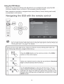
1
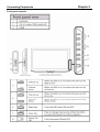
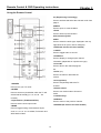
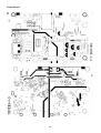
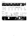
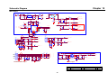
Acer AT2230 & AT2231
Service Guide
1
Service Guide Version and Revision
Version
Date
Revision History
TPV Model Name
A00
Jul.-23-08
Initial release
E228M3NBWAZANN
A01
Aug.-03-08
Add FRU List
E228M3NBWAZANN
2
Copyright
Copyright 2003 Acer Technology Corp.
All rights reserved.
This manual may not, in whole or in part, be copied, photocopied, reproduced, translated, or converted to any
electronic machine readable form without prior written permission of Acer Technology Corp.
ACER AT2230 & AT2231 Service Manual.
Printed in Fujian.
Disclaimer
The information in this guide is subject to change without notice. Acer Incorporated makes no representations or
warranties, either expressed or implied, with respect to the contents hereof and specifically disclaims any warranties
of merchantability or fitness for any particular purpose. Any Acer Incorporated software described in this manual is
sold or licensed "as is". Should the programs prove defective following their purchase, the buyer (and not Acer
Incorporated, its distributor, or its dealer) assumes the entire cost of all necessary servicing, repair, and any
incidental or consequential damages resulting from any defect in the software.
Acer is a registered trademark of Acer Corporation.
Intel is a registered trademark of Intel Corporation.
Pentium and Pentium II/III are trademarks of Intel Corporation.
Other brand and product names are trademarks and/or registered trademarks of their respective holders.
Trademarks
All other trademarks are property of their respective owners.
Conventions
The following conventions are used in this manual:
Screen messages
NOTE
WARNING
CAUTION
IMPORTANT
Denotes actual messages that appear on screen.
Gives bits and pieces of additional information related to the current topic.
Alerts you to any damage that might result from doing or not doing specific
actions.
Gives precautionary measures to avoid possible hardware or software
problems.
Remind you to do specific actions relevant to the accomplishment of
procedures.
3
Preface
Before using this information and the product it supports, please read the following general information.
1. This Service Guide provides you with all technical information relating to the BASIC CONFIGURATION decided
for Acer's "global" product offering. To better fit local market requirements and enhance product competitiveness,
your regional office may have decided to extend the functionality of a machine (e.g. add-on card, modem, or extra
memory capability). These LOCALIZED FEATURES will NOT be covered in this generic service guide. In such
cases, please contact your regional offices or the responsible personnel/channel to provide you with further
technical details.
2. Please note WHEN ORDERING FRU PARTS, that you should check the most up-to-date information available on
your regional web or channel. If, for whatever reason, a part number change is made, it will not be noted in the
printed Service Guide. For ACER-AUTHORIZED SERVICE PROVIDERS, your Acer office may have a
DIFFERENT part number code to those given in the FRU list of this printed Service Guide. You MUST use the list
provided by your regional Acer office to order FRU parts for repair and service of customer machines.
Warning: (For FCC Certified Models)
Note: This equipment has been tested and found to comply with the limits for a Class B digital device, pursuant to
Part 15 of the FCC Rules. These limits are designed to provide reasonable protection against harmful interference in
a residential installation. This equipment generates uses and can radiate radio frequency energy, and if not installed
and used in accordance with the instructions, may cause harmful interference to radio communications. However,
there is no guarantee that interference will not occur in a particular installation. If this equipment does cause harmful
interference to radio or television reception, which can be determined by turning the equipment off and on, the user
is encouraged to try to correct the interference by one or more of the following measures:
1. Reorient or relocate the receiving antenna.
2. Increase the separation between the equipment and receiver.
3. Connect the equipment into an outlet on a circuit different from that to which the receiver is connected.
4. Consult the dealer or an experienced radio/TV technician for help.
Notice:
1. The changes or modifications not expressly approved by the party responsible for compliance could void the
user's authority to operate the equipment.
2. Shielded interface cables and AC power cord, if any, must be used in order to comply with the emission limits.
3. The manufacturer is not responsible for any radio or TV interference caused by unauthorized modification to this
equipment. It is the responsibility of the user to correct such interference.
As ENERGY STAR® Partner our company has determined that this product meets the ENERGY STAR®
guidelines for energy efficiency.
Warning:
To prevent fire or shock hazard, do not expose the monitor to rain or moisture. Dangerous high voltages are
present inside the monitor. Do not open the cabinet. Refer servicing to qualified personnel only.
4
Precautions
z Do not use the monitor near water, e.g. near a bathtub, washbowl, kitchen sink, laundry tub, swimming pool or in
a wet basement.
z Do not place the monitor on an unstable trolley, stand, or table. If the monitor falls, it can injure a person and
cause serious damage to the appliance. Use only a trolley or stand recommended by the manufacturer or sold
with the monitor. If you mount the monitor on a wall or shelf, uses a mounting kit approved by the manufacturer
and follow the kit instructions.
z Slots and openings in the back and bottom of the cabinet are provided for ventilation. To ensure reliable
operation of the monitor and to protect it from overheating, be sure these openings are not blocked or covered.
Do not place the monitor on a bed, sofa, rug, or similar surface. Do not place the monitor near or over a radiator
or heat register. Do not place the monitor in a bookcase or cabinet unless proper ventilation is provided.
z The monitor should be operated only from the type of power source indicated on the label. If you are not sure of
the type of power supplied to your home, consult your dealer or local power company.
z The monitor is equipped with a three-pronged grounded plug, a plug with a third (grounding) pin. This plug will fit
only into a grounded power outlet as a safety feature. If your outlet does not accommodate the three-wire plug,
have an electrician install the correct outlet, or use an adapter to ground the appliance safely. Do not defeat the
safety purpose of the grounded plug.
z Unplug the unit during a lightning storm or when it will not be used for long periods of time. This will protect the
monitor from damage due to power surges.
z Do not overload power strips and extension cords. Overloading can result in fire or electric shock.
z Never push any object into the slot on the monitor cabinet. It could short circuit parts causing a fire or electric
shock. Never spill liquids on the monitor.
z Do not attempt to service the monitor yourself; opening or removing covers can expose you to dangerous
voltages and other hazards. Please refer all servicing to qualified service personnel
z To ensure satisfactory operation, use the monitor only with UL listed computers which have appropriate
configured receptacles marked between 100 - 240V AC, Min. 5A.
z The wall socket shall be installed near the equipment and shall be easily accessible.
Special Notes On LCD TV Monitors
The following symptoms are normal with LCD TV monitor and do not indicate a problem.
Notes
z Due to the nature of the fluorescent light, the screen may flicker during initial use. Turn off the Power Switch and
then turn it on again to make sure the flicker disappears.
z You may find slightly uneven brightness on the screen depending on the desktop pattern you use.
z The LCD TV screen has effective pixels of 99.99% or more. It may include blemishes of 0.01% or less such as a
missing pixel or a pixel lit all of the time.
z Due to the nature of the LCD TV screen, an afterimage of the previous screen may remain after switching the
image, when the same image is displayed for hours. In this case, the screen is recovered slowly by changing the
image or turning off the Power Switch for hours.
5
Table Of Contents
Chapter 1
Monitor Features
………………………………………
7
General Specifications
………………………………………
7
LCD TV Description
………………………………………
8
Precautions And Notices
………………………………………
8
D-SUB / HDMI Digital connector
………………………………………
9
Factory Preset Display Modes
………………………………………
10
LCD TV Panel Specification
………………………………………
11
Panel Features
………………………………………
11
General Specifications
………………………………………
11
Mechanical Specifications
………………………………………
11
Optical Specifications
………………………………………
12
Connecting Peripherals
………………………………………
13
Front Panel Controls
…………………………………………..
13
………………………………………………….
14
………………………………………
14
Chapter 2
Remote Control & OSD Operating
Chapter 3
Instructions
Using The Remote Control
Using The OSD Menus
16
Chapter 4
Machine Disassembly
………………………………………
23
Chapter 5
Trouble Shooting
………………………………………
27
Chapter 6
Upgrade Firmware
………………………………………
33
Chapter 7
White-Balance, Luminance Adjustment
………………………………………
36
FRU (Field Replaceable Unit) List
………………………………………
40
Exploded Diagram
………………………………………
40
EDID Data
………………………………………
43
Chapter 9
PCB Layout
………………………………………
44
Chapter 10
Schematic Diagram
………………………………………
48
Chapter 8
6
Chapter 1
Monitor Features
General Specifications
7
LCD TV Description
The LCD TV will contain a main board, a power board a function keyboard and an IR board. The main board and
power board will house the flat panel to control logic I2C bus, DDC, brightness control logic for LCD panel, DC-DC
conversion to supply the appropriate power to the whole board and transmitting TTL level signals into LCD Module
to drive the LCD display circuit.
The inverter board will drive the five CCFLs (Cold Cathode Fluorescent Lamp).
The function keyboard and Remote Control will provide the OSD control signal to the Main Board.
Precautions And Notices
1-1 Assembly Precaution
(1) Please do not press or scratch LCD panel surface with anything hard. And do not soil LCD panel surface
by touching with bare hands (Polarize film, surface of LCD panel is easy to be flawed)
In the LCD panel, the gap between two glass plates is kept perfectly even to maintain display
characteristic and reliability. If this panel is subject to hard pressing, the following occurs :
(a) Uniform color
(b) Orientation of liquid crystal becomes disorder
(2) Please wipe out LCD panel surface with absorbent cotton or soft cloth in case of it being soiled.
(3) Please wipe out drops of adhesive like saliva and water in LCD panel surface immediately.
They might damage to cause panel surface variation and color change.
(4) Do not apply any strong mechanical shock to the LCD panel.
1-2 Operating Precaution
(1) Please be sure to unplug the power cord before remove the back-cover. (be sure the power is turn-off)
(2) Please do not change variable resistance settings in MAIN-BOARD; they are adjusted to the most suitable
value. If they are changed, it might happen LUMINANCE does not satisfy the white balance spec.
(3) Please consider that LCD backlight takes longer time to become stable of radiation characteristic in low
temperature than in room temperature.
(4) Please pay attention to displaying the same pattern for very long-time. Image might stick on LCD.
1-3 Storage Precaution
(1) When you store LCD for a long time, it is recommended to keep the temperature between -20°C - 60°C
without the exposure of sunlight and to keep the humidity less than 85% RH.
(2) Please do not leave the LCD in the environment of high humidity and high temperature such as 60°C,
95%RH.
(3) Please do not operate the LCD in the environment of abnormal temperature, below 0°C.
1- 4 High Voltage Warning
The high voltage was only generated by Power support part, if carelessly contacted the transformer on this
module, can cause a serious shock.
8
D-SUB PIN Distribution
This procedure gives you instructions for installing and using the LCD TV display.
(1) Position the display on the desired operation and plug the power cord into a convenient AC outlet. Three-wire
power cord must be shielded and is provided as a safety precaution as it connects the chassis and cabinet to
the electrical conduct ground. If the AC outlet in your location does not have provisions for the grounded type
plug, the installer should attach the proper adapter to ensure a safe ground potential.
(2) Connect the 15-pin color display shielded signal cable to your signal system device and lock both screws on the
connector to ensure firm grounding. The connector information is as follow:
15 - Pin Color Display Signal Cable
Pin NO.
1
Description
Pin NO.
Description
Red video input
9
DDC +3.3V (or 5V)
2
Green video input /SOG
10
Logic ground
3
Blue video input
11
GND
4
GND
12
Serial data line (SDA)
5
GND– cable detect
13
H. Sync / H+V
6
Red video ground
14
V. Sync
7
Green video ground
15
Data clock line (SCL)
8
Blue video ground
HDMI Digital connector pin assignments
Pin No.
Description
Pin No.
Description
1
TMDS Data2+
2
TMDS Data2 Shield
3
TMDS Data2-
4
TMDS Data1+
5
TMDS Data1 Shield
6
TMDS Data1-
7
TMDS Data0+
8
TMDS Data0 Shield
9
TMDS Data0-
10
TMDS Clock+
11
TMDS Clock Shield
12
TMDS Clock-
13
CEC
14
NC
15
SCL
16
SDA
17
DDC/CEC Ground
18
+5V Power
19
Hot Plug Detect
9
Factory Preset Display Modes:
Analog RGB Signal Timing
10
LCD TV Panel Specification
The M220Z1-L03 model is a 22 inch wide TFT-LCD module with a 4-CCFL Backlight Unit and a 30-pin 2ch-LVDS
interface. This module supports 1680 x 1050 WSXGA+ (16:10 wide screen) mode and displays up to 16.7 millions
colors. The inverter module for the Backlight Unit is not built in.
Panel Features
-Super wide viewing angle
- High contrast ratio
- Fast response time
- High color saturation (EBU Like Specifications)
- WSXGA+ (1680 x 1050 pixels) resolution
- DE (Data Enable) only mode
- LVDS (Low Voltage Differential Signaling) interface
General Specifications
Mechanical Specification
11
Optical Specifications
Test Conditions
Optical Specifications
12
Chapter 2
Connecting Peripherals
Front panel controls
13
Remote Control & OSD Operating instructions
Chapter 3
Using the Remote Control
5 e (Empowering Technology)
Press to activate and select the scenario mode. See
page 9.
6 MENU
Press to open or close the Menu.
7 Back
Press to back to previous Menu.
8 Directional keys/OK
9 MPX
Press to select the audio type, displayed in the top
right-hand corner (mono, stereo, bilingual).
10 EPG (No function for these models)
11 MUTE
Press to toggle audio on and off.
12 DISPLAY
Press to display or change input/ channel
information (dependent on input/source type).
13 CH LIST
Press to launch the channel/program
list.
14 VOL (+/-)
Press to increase or decrease the
volume.
.
15 CH (up/down)
Press to sequentially select the TV
1 POWER
channel.
Press to turn your TV on/off.
16 Audio effects
2 SLEEP
Press to turn audio mode to Surround
Press to set a time period after which the TV will
mode.
switch itself to standby (5, 0, 5, 20, 25 ... 80
17 Number keys.
minutes).
18 RECALL
3 Input buttons (TV/AV/SCART/PC)
Press to return to the previous channel.
Press to select correct input mode.
19 ENTER (No function for these models)
4 WIDE
Press to toggle scaling mode between Super
zoom, 4:3, 4:9, 6: 0, 6: 0 subtitle, Full screen and
Wide detect modes.
14
Teletext
1 Colour buttons (R/G/Y/B)
Operates corresponding button on the teletext page.
2 INDEX
Press to go to the index page.
3 SUBTITLE
Press to view subtitles on the screen.
4 REVEAL
Press to reveal hidden teltext information.
5 SUBPAGE
Press to access the teletext’s subpages directly.
6 SIZE
Press once to zoom teletext page to 2X. Press again to resume.
You can also use navigation key (up and down) to zoom-in or zoom-out the teletext page.
7 TTX/MIX (TELETEXT/MIX)
Press to switch from TV/AV to Teletext mode.
Press to overlay teletext page on the TV image.
8 HOLD
Press to pause the current teletext page in multi-page viewing mode.
15
Using the OSD Menus
16
17
18
19
20
21
How To Optimize The DOS-Mode
Plug And Play
Plug & Play DDC2B Feature
This monitor is equipped with VESA DDC2B capabilities according to the VESA DDC STANDARD. It allows the
monitor to inform the host system of its identity and, depending on the level of DDC used, communicate additional
information about its display capabilities.
The DDC2B is a bi-directional data channel based on the I²C protocol. The host can request EDID information over
the DDC2B channel.
This monitor will appear to be non-functional if there is no video input signal. In order for this monitor to
operate properly, there must be a video input signal.
This monitor meets the Green monitor standards as set by the Video Electronics Standards Association (VESA)
and/or the United States Environmental Protection Agency (EPA) and The Swedish Confederation Employees
(NUTEK). This feature is designed to conserve electrical energy by reducing power consumption when there is no
video-input signal present. When there is no video input signals this monitor, following a time-out period, will
automatically switch to an OFF mode. This reduces the monitor's internal power supply consumption. After the video
input signal is restored, full power is restored and the display is automatically redrawn. The appearance is similar to
a "Screen Saver" feature except the display is completely off. The display is restored by pressing a key on the
keyboard, or clicking the mouse.
Using the Right Power Cord
The accessory power cord for the Northern American region is the wallet plug with NEMA 5-15 style and is UL listed
and CSA labeled. The voltage rating for the power cord shall be 125 volts AC.
Supplied with units intended for connection to power outlet of personal computer: Please use a cord set consisting of
a minimum No. 18 AWG, type SJT or SVT three conductors flexible cord. One end terminates with a grounding type
attachment plug, rated 10A, 250V, CEE-22 male configuration. The other end terminates with a molded-on type
connector body, rated 10A, 250V, having standard CEE-22 female configuration.
Please note that power supply cord needs to use VDE 0602, 0625, 0821 approval power cord in European counties.
22
Chapter 4
Machine Disassembly
This chapter contains step-by-step procedures on how to disassemble the monitor for
maintenance.
The tools listed as below are that we may use during this procedure:
1. A proper screwdriver
2. A pair of glove
3. A pliers
4. A plastic knife
Disassembly Procedure
Disassemble the Base
1. Put the monitor on a clean soft cloth with panel facing to the table. (Fig 1)
(Fig 1)
2. Remove the screws to remove stand base. (Fig 2-3)
(Fig 2)
(Fig 3)
23
Disassemble the back cover
1. Remove four screws to remove back cover. (Fig 4)
(Fig 4)
Remove the Shielding-EMI
(Fig 5)
24
Remove the main board, power board and key board.
1. Release all the connecting wires marked in blue for these boards. (Fig 6)
2. Remove the screws marked in red to remove power board and main board. (Fig 6)
3. Remove the key board. (Fig 7)
(Fig 6)
Key board
(Fig 7)
Disassemble the speaker.
Remove the four screws marked in red to remove the speakers. (Fig 8-9)
(Fig 8)
(Fig 9)
25
Remove the main frame
Remove the four screws marked in red to remove the main frame.
(Fig 10)
(Fig 11)
Disassemble the IR board
(Fig 12)
Disassemble the front panel
(Fig 13)
26
Chapter 5
Trouble Shooting
No picture (LED orange)
No picture
OK
Check key board/IR board
NG
Change key board/IR board
OK
NG
Check the power supply circuit
Check 24V power supply
OK
NG
Check main board Standby power supply
Change U707
OK
Check U401
NG
Change U401
OK
NG
Check I2C communication
Check I2C bus
27
Abnormal display
Reset source
Check the source
OK
NG
Check signal filter circuit
Replace the filter or resistance
OK
OK
NG
RF signal
Check input
OK
Check LVDS cable
OK
NG
Replace LVDS cable
OK
Check panel
Check TV system setup
Check Tuner
OK
NG
Replace panel
28
Replace Tuner
No sound
Check the source
NG
Reset source
OK
Check if mute
OK
Check input signal
Check TV
TV SIF
system
NG
OK
NG
OK
Check U601
Change TU101
Check TU101
Check U401
Change U401
NG
Change U601
OK
NG
Check speaker
NG
Change speaker
29
Reset TV system
No Power (No LED indicator)
Check CN902 pin10,11 = 12V
NG
Check AC line volt 110V or 220V
NG
OK
Check AC input
Check the voltage of C905 (+)
OK
NG
Check bridge rectified circuit and F901 circuit
Check start voltage for the pin8 of IC901
OK
NG
Check R904, R905 and Change IC901
Check the auxiliary voltage is bigger than
10V and smaller than 20V
OK
NG
1) Check IC901, D902, C908
2) Check IC902 OVP circuit
Check IC901 pin5 PWM wave
OK
NG
Check IC901
Check T901, Q903, D906, D904, ZD920, IC903
30
W / LED, No Backlight
Check 12V input
NG
Check adapter or MB
OK
Check ON/OFF
NG
Check Interface board
OK
Check IC801
NG
Change ON/OFF
OK
Check IC801 PIN1.15 have the output of square wave at short time
NG
Change IC801
OK
Check the input of Q805, Q806
NG
Change Q805, Q806,D801,D802,D803,Q804
OK
Check the output of PT802
NG
Change PT802
OK
Check connector & lamp
31
Key Board
OSD is unstable or not working
N
Is Key Pad Board connecting normally?
Connect Key Pad Board
Y
N
Is Button Switch normally?
Replace Button Switch
Y
N
Is Key Pad Board Normally?
Y
Check Main Board
32
Replace Key Pad Board
Chapter 6
Upgrade Firmware
1. Using USB port connecting PC & MST99980 Board via ISP board as below. Turn on the monitor.
2. Run the program ISP_Tool.
33
3. Click the button “Connect”, if it can identify the type of the device, please click the “Dis Con” and then click the
“Connect” again.
34
4. Click the button “Read” to load the software file and then click the “Auto”.
35
5. When the picture showed as below, we can click the “run” to finish to upgrading.
36
White-Balance, Luminance Adjustment
Chapter 7
Approximately 30 minutes should be allowed for warm up before proceeding white balance adjustment.
YPbPr Mode display adjustment
White balance adjustment (B)
General set-up:
Equipment Requirements: Minolta CA-110 or Equivalent Color analyzer
Quantum Data Pattern Generator 802G, 802BT or equivalent instrument
Input requirements:
Input Signal Type: YPbPr signal
1. 720P mode, TVBar100 pattern by 802G or 802BT.
2. Select Smart picture to User mode and check the x, y data.
Input Signal Strength: 1 Vpp for Y signal; 700 mVpp for Pb & Pr signal
Input Injection Point: YPbPr (RAC jack)
720P, TVBar100 pattern
`
Alignment method:
Initial Set-up:
1. Select source as “Component”.
2. Set Smart picture as “User” and to be Contrast =50(TBD) (CMO), Brightness=50(TBD) (CMO), at normal menu
mode.
3. Apply “TVBar100” pattern with color bar pattern by signal generator.
4. Enter factory mode menu: press “MENU+ “234” then enter FAC mode.
Alignment:
1. At FAC mode menu, select FACTORY->Picture ->ADC -> Auto Colour item. Then press “>” key to adjust
ADC_GAIN_R, ADC_GAIN_G, ADC_GAIN_B and ADC_OFFSET_R, ADC_OFFSET_G, ADC_OFFSET_B. Then
37
store those values to NVM.
White- Balance alignment:
1. Select source as “HDMI1”
2. Apply Flat pattern (100% white pattern), at FAC mode menu, select Factory -> Picture -> Colour Temp item
3. Set color temperature to “Standard”.
4. Adjust the R Gain, G Gain, B Gain values to meet “Standard” color coordinates specification below. Then store
those values to NVM.
5. Set color temperature to “Warm”.
6. Adjust the R Gain, G Gain, B Gain values to meet “Warm” color coordinates specification below. Then store
those values to NVM.
7. Set color temperature to “Cold”.
8. Adjust the R Gain, G Gain, B Gain values to meet “Cold” color coordinates specification below. Then store
those values to NVM.
Color temperature Standard/Warm/Cold (x, y) co-ordinates specification:
Picture Mode
x
Y
Standard(6500oK)
0.314±0.015
0.329±0.015
Warm (5500oK)
0.332±0.015
0.341±0.015
Cold (7500oK)
0.300±0.015
0.310±0.015
Table: Reading with Minolta CA-110.
Note:
1. Use Minolta CA-110 for colour coordinates and luminance check.
2. Luminance > 250 cd/m2 in the center of the screen when Brightness control at 100; Contrast control at 100
3. Reset AV setting, smart picture shall be recalled to be “Standard” and Contrast=50 (CMO), Brightness=50
(CMO)
38
PC mode display adjustment
WHITE-D adjustment (B)
General set-up:
Equipment Requirements: Minolta CA-110 or Equivalent Color analyzer
Chroma 2250 or equivalent PC signal generator
Input requirements:
Input Signal Type: PC VGA signal
1024X768/60Hz PC mode with PGCWRGB pattern. (see pattern-1)
Input Signal Strength: 0.7 Vp-p linear voltage.
Input Injection Point: PC D-SUB input
Pattern-1
Alignment method:
Initial Set-up:
1. Select source as “VGA”.
2. Set Contrast = 50 (CMO) and Brightness=50 (CMO), at Standard menu mode.
3. Apply “PGCWRGB”(pattern-1) pattern by VGA pattern generator.
4. Enter factory mode menu: press “MENU+ “234” then enter FAC mode
Alignment:
1. At FAC mode menu, select FACTORY->Picture ->ADC -> Auto Colour item. Then press “>” key to adjust
ADC_GAIN_R, ADC_GAIN_G, ADC_GAIN_B and ADC_OFFSET_R, ADC_OFFSET_G, ADC_OFFSET_B. Then
store those values to NVM.
39
Chapter 8
FRU (Field Replaceable Unit) List
This chapter gives you the FRU (Field Replaceable Unit) listing in global configurations of AT2230 & AT2231.Refer
to this chapter whenever ordering for parts to repair or for RMA (Return Merchandise Authorization).
NOTE: Please note WHEN ORDERING FRU PARTS that you should check the most up-to-date information
available on your regional web or channel (http://aicsl.acer.com.tw/spl/). For whatever reasons a part number
change is made, it will not be noted in the printed Service Guide. For ACER AUTHORIZED SERVICE PROVIDERS,
your Acer office may have a different part number code from those given in the FRU list of this printed Service Guide.
You must use the local FRU list provided by your regional Acer office to order FRU parts for repair and service of
customer machines.
NOTE: To scrap or to return the defective parts, you should follow the local government ordinance or regulations on
how to dispose it properly, or follow the rules set by your regional Acer office on how to return it.
Exploded Diagram (Model: AT2230 & AT2231)
40
Part List
Above picture show the description of the following component.
Item
Picture
Description
1
Bezel
2
Panel
3
Base
4
Power Board
41
5
Main Board
6
Key Board
7
IR Board
8
Speaker
42
EDID Data
DDC DATA for D-Sub Input
43
Chapter 9
PCB Layout
Main Board
44
45
Power Board
46
Key Board
IR board
47
Chapter 10
Schematic Diagram
Main Board
+12V
V5A
L102
300 OHM
R187
27 OHM 2W
R188
33 OHM 2W
L101
300 OHM
U103
AP1084D50L13
3
1
+
C160
C158
0.1uF 10UF16V
V5B
R189
0 OHM 1/10W
2
INPUT OUTPUT
V5C
ADJ/GND
L103
300 OHM
+
C161
0.1uF
C159
47uF/16V
V5C
TV-CVBS
R191
NC
Q107
NC
R190
47 OHM 1/16W
R194
NC
V5B
+
I2C_SCL
I2C_SDA
R200
100 OHM 1/10W
+5V
4
5
6
13
TU101
C167
NC
VIDEO_OUT 4
C166
0.047uF
TUNER_CVBS 8
R199
NC
R203
47 OHM 1/16W
SCL
SDA
C163
47uF/16V
AF_O/P
SIFSND
AS_TU
N.C
N.C
N.C
AS_IF
C169 VCOM0
0.047uF
VCOM0
8
TUNER
SIF
CVBS
12
R205
0 OHM 1/16W
C171
0.1uF25V
R207
0 OHM 1/16W
C173
0.1uF25V
SIFP0
8
TV-CVBS
R198
NC
T1AF
T1SIF
14
11
R206
NC
SIF
C172
CLOSE to CHIP
22pF
R101
47 OHM 1/10W
1
2
9
10
C170
100pF
SIFM0
8
R204
1K OHM 1/10W
15
16
17
18
TH1
TH2
TH3
TH4
8,12
8,12
I2C_SCL
I2C_SDA
C165
0.1uF
+5V IF
3
C164
0.1uF
R193
10K OHM 1/10W
R197
100 OHM 1/10W
R202
75 OHM 1/8W
C168
680pF
+
C162
47uF/16V
R192
10K OHM 1/10W
R196
47 OHM 1/16W
V5C
R201
NC
V5A
R195
0 OHM 1/8W
EMI
FB107
300 OHM
FB108
300 OHM
VCOM1_1
R215
47 OHM 1/16W
C181 0.047uF
AV1
R208
R209
0 OHM 1/8W
47 OHM 1/16W
C194
R210
22pF
75 OHM 1/8W
R211
10K OHM 1/10W
C174 0.047uF
VCOM1
8
CVBS1
8
CN104
JACK
2
C176
22pF
C189
22pF
4
AUL0_AV
8
R212
12K OHM 1/10W
2.2uF
C178
R213
10K OHM 1/10W
AUR0_AV
8
R224
10K OHM 1/10W
C192
22pF
1
C115
10pF
R136
75 OHM 1/8W
R135
75 OHM 1/8W
R134
75 OHM 1/8W
5
VPORT0603100KV05
3
VPORT0603100KV05
D112
4
D110
Y
C191
2.2uF
AUR0_COM
8
R225
12K OHM 1/10W
C180
560pF
2
6
8
R214
12K OHM 1/10W
VPORT0603100KV05
D111
Pb
AUL0_COM
C193
560pF
CN103
JACK
Pr
C188
2.2uF
C190
560pF
R223
12K OHM 1/10W
3
2.2uF
C175
C177
560pF
C179
22pF
R222
10K OHM 1/10W
1
VPORT0603100KV05
D120
EMI
VPORT0603100KV05
D117
VPORT0603100KV05
D118
VPORT0603100KV05
D119
2
7 VCOM1_1
9
8
4
6
5
1
3
VPORT0603100KV05
D121
CN102
JACK
C116
10pF
R130
47 OHM 1/10W
R131
47 OHM 1/10W
R132
47 OHM 1/10W
R133
470 OHM 1/10W
C112
0.047uF
C113
0.047uF
C114
0.047uF
C101
0.001uF
Y+
8
PR+
8
PB+
8
SOY
8
R221
47 OHM 1/16W
C187
0.047uF
SV_C0
CN105
R216
47 OHM 1/16W
R219
75 OHM 1/8W
C183
NC
C184
47pF
4
3
2
1
6
R217
47 OHM 1/16W
5
C185
47pF
S-LUM0
C186
NC
DIN JACK
C182
SV_Y 0
0.047uF
SV_C0
8
SV_Y 0
8
R220
75 OHM 1/8W
C117
10pF
D122
VPORT0603100KV05
R218
47 OHM 1/16W
SV GND Reference to VCOM0
D123
VPORT0603100KV05
S-Video Input
AUDIO&VIDEO Input
T P V ( Top
Victory
Electronics
絬隔瓜絪腹
Key Component
Date
48
03 Video Input
Tuesday , July 22, 2008
Co . ,
Ltd. )
OEM MODEL Acer AT1930/2230
Size
A3
TPV MODEL
Rev
1.0
称爹
<称爹>
PCB NAME
Sheet
715T2849-1
3
of
12
2
1
2
1
D114
BAV99
D115
BAV99
D116
BAV99
3
3
CVBS INPUT
3
D113
BAV99
3
2
1
2
1
+5V
CN106
SCART
C123
47pF
C124
47pF
C125
47pF
15
Red I/O
14
R144
75 OHM 1/8W
C122
47pF
17
16
R143
75 OHM 1/8W
19
18
R142
75 OHM 1/8W
R141
75 OHM 1/8W
21
20
R137
47 OHM 1/16W
R138
47 OHM 1/16W
R139
47 OHM 1/16W
R140
47 OHM 1/16W
C118
0.047uF
C119
0.047uF
C120
0.047uF
C121
0.047uF
SC_CVBS
SCR+
SCG+
SCB+
SC_CVBS
8
SCR+
8
SCG+
8
SCB+
8
2Vp-p
13
11
Green I/O
CVBS OUT
Blue I/O
C128
47pF
R145
75 OHM 1/10W
10
TV CVBS Output
C129
100uF/16V
TVOUT2
+
12
9
2
8
7
+5V
FB109
1
FB105
600 OHM
V8AUD
6
1
C131
0.001uF
FB110
Audio R-Out
1
2
R148
10K OHM 1/10W
C130
2.2uF
300 OHM
1
C132
NC
C133
560pF
AUL1
8
C134
0.1uF
CLOSE TO CHIP
R151
10K OHM 1/16W
R150
12K OHM 1/10W
300 OHM
SCART_ARin1
R154
10K OHM 1/10W
C138
0.001uF
2
C139
NC
C135
2.2uF
AUR1
C141
560pF
3
R156
47K OHM 1/10W
8
C142
100uF/16V
1uF
U102
2
R160
47K OHM 1/10W
SC_FS
8
C144
4.7uF
R165
C145
680 OHM 1/10W 4.7uF
LineMute
R167
Q105
R174
R166
4.7K OHM 1/10WPMBS3904
100K OHM 1/10W
NC
R169
4.7K OHM 1/10W
SC_FSW
SC_FSW
Gainx2
R157
10K OHM 1/16W
1
R170
33K OHM 1/10W
C148
100pF
R171
10K OHM 1/10W
C147 4.7uF
5
R176
47K OHM 1/10W
+
R168
100 OHM 1/10W
C151
4.7uF
R178
680 OHM 1/10W
C152
4.7uF
7
- 6
R163
75 OHM 1/8W
C149
10
LineMute
0.001uF R173
100K OHM 1/10W
LineMute
R180
Q106
4.7K OHM 1/10W PMBS3904
100K OHM 1/10W R182
NC
R181
R184
47K OHM 1/10W
LM358D
C154 C153
1uF
2.2uF
R177
47K OHM 1/10W
R185
33K OHM 1/10W
C157
100pF
R172
100 OHM 1/10W
R175
22K OHM 1/10W
close
to
audio
amp
R186
10K OHM 1/10W
T P V ( Top
Victory
Electronics
絬隔瓜絪腹
Key Component
Date
04 SCART & Y PbPr Input
Tuesday , July 22, 2008
Co . ,
C155 4.7uF
Ltd. )
SCART OutL0
10
C150
0.01uF
Placement Near
MST.IC DAC
output Pad
R179
100 OHM 1/10W
R183
22K OHM 1/10W
49
R159
75 OHM 1/16W
+ 3
4.0V
8
AUDIO_OUT_R
C137
47pF
R161
100 OHM 1/10W
C146
0.001uF R164
100K OHM 1/10W
R162
1.5K OHM 1/10W
Blanking I/O
AUDIO_OUT_L
4
C136
47pF
SC_FS
R149
75 OHM 1/16W
C140
10UF16V
+
R158
10K OHM 1/10W
Q104
PMBS3904
R152
NC
VIDEO_OUT
C143
R155
12K OHM 1/10W
Switch
Q103
PMBS3906
C127
R146
10UF16V 470 OHM 1/16W
+
3
2
8
Audio L-Input
Audio R-Input
Audio L-Out
5
4
C126 +
0.1uF
SCART OutR0 10
C156
0.01uF
OEM MODEL Acer AT1930/2230
Size
A3
TPV MODEL
Rev
1.0
称爹
<称爹>
PCB NAME
Sheet
715T2849-1
4
of
12
R831
0 OHM 1/16W
TXD
8,12
R832
0 OHM 1/16W
RXD
8,12
17
CN107
DB15
1
6
2
7
3
8
4
9
5
10
11
12
13
14
15
R11047 OHM 1/16W C107 0.047uF
G
R11147 OHM 1/16W C108 0.047uF
B
R11247 OHM 1/16W C109
R114 R115 R116
75 OHM 1/8W 75 OHM 1/8W
75 OHM 1/8W
VPORT0603100KV05
VPORT0603100KV05
VPORT0603100KV05
VGA5V
D103 D104 D105
D102
16
R
RIN+
0.047uF
R113
C110 1000pF
470 OHM 1/16W
8
GIN+
8
BIN+
8
SOG
8
R833
0 OHM 1/8W
NC
R-
R834
0 OHM 1/8W
GB-
ZD106 ZD107
TZMC5V6TZMC5V6
DDC_SCL
1
FB106
300 OHM
EMI
VGA5V 2
D101
3
BAT54C
C111
0.1uF25V
U101
C195
0.1uF25V
1
2
3
4
A0 VCC
A1
WP
A2 SCL
VSS SDA
8
7
6
5
R126
100 OHM 1/16W
DDC_SDA
R128
4.7K OHM 1/16W
R125
100 OHM 1/16W
+5V
R121
4.7K OHM 1/16W
ZD108 ZD109
TZMC5V6TZMC5V6
R122
4.7K OHM 1/16W
VGA_PW
R117
100 OHM 1/16W
R118
2.2K OHM 1/16W
R119
VSI
100 OHM 1/16W
R120
2.2K OHM 1/16W
HS_RGB
HSI
HS_RGB
8,12
VS_RGB
8,12
VS_RGB
EMI
C196
22pF
C197
22pF
R123
NC
RXD
R124
NC
TXD
RXD
8,12
TXD
8,12
R127
NC
Q108
PMBS3904
R835
10K OHM 1/16W
HDMI_WP
6,8
M24C02-WMN6TP
R129
NC
T P V ( Top
Victory
Electronics
絬 隔 瓜絪 腹
Key Component
Date
05 VGA
Tuesday , July 22, 2008
50
Co . ,
Ltd. )
OEM MODEL AT1930/2230
Size
A4
TPV MODEL
Rev
1.0
称爹
<称爹>
PCB NAME
Sheet
715T2849-1
5
of
12
24C02=>EDID code must
be upto 256byte space,
for HDMI interface.
HDMI-1
CN502
TMDSD2TMDSD2+
TMDSD1TMDSD1+
TMDSD0TMDSD0+
DDC_CLK_IN1
DDC_DAT_IN1
CEC_INA
HPD1
U502
8
7
6
5
R514
100 OHM 1/16W
100 OHM 1/16W
R515
D507
19
13
16
15
D508
D509
2
3
90 ohm
4
L510
3
1
HDMI_02HDMI_02+
6
4
HDMI_01HDMI_01+
1
2
9
7
HDMI_RXC+_1
5
4
IN4
IN3
2
1
3
90 ohm
L511
Q504
PMBS3904
C501
0.1uF
R543
IN2
IN1
HDMI_00HDMI_00+
1
4
2
3
90 ohm
L512
1
4
2
HDMI_RX2+_1
HDMI_RX2-_1
5
4
HDMI_RX1+_1
HDMI_RX1-_1
2
1
HDMI_RX0-_1
8
8
+3.3_SUB
OUT4
OUT3
OUT2
OUT1
HPLUGA
6
7
9
10
EMI
8
HDMI_RX0+_1 8
HDMI_RX0-_1 8
CEC_INB R522
0 OHM 1/10W
HDMI_RXC+_1 8
HDMI_RXC-_1 8
CEC_INA R523
0 OHM 1/10W
IN4
IN3
IN2
IN1
OUT4
OUT3
OUT2
OUT1
6
7
TMDSD1TMDSD1+
TMDSD0TMDSD0+
D504
D505
R506
47K OHM 1/10W
R507
47K OHM 1/10W
R504
4.7K OHM 1/10W
NC
47pF
CEC
8
SUBCEC
12
100 OHM 1/10W
R526
C507
EMI
NC
R527
100 OHM 1/16W
NC
C506
NC
ZD511
ZMM5V6
C508
EMI
NC
+5V_STB
HD_+5V2
NC
HD5V2
EMI C504
R530
0.1uF25V
0 OHM 1/10W
3
HD_+5V2
C509
2 HD5V2
C502
0.1uF
8
7
6
5
R512
100 OHM 1/10W
VPORT0603100KV05
VPORT0603100KV05
VPORT0603100KV05 VPORT0603100KV05
2
1
HDMI_RX2-_3
IN4
IN3
3
8
5
4
GND
HDMI_RXC-_3
HDMI_RXC+_3
1
2
3
4
Q505
PMBS3904
R544
10K OHM 1/16W
R539 22 OHM 1/16W R540 22 OHM 1/16W
R541 22 OHM 1/16W R542 22 OHM 1/16W
EMI
C510
Q501
PMBS3904
GND
12
10
A0
A1
A2
GND
R516
100 OHM 1/10W
R517
100 OHM 1/10W
DDC_SDA2
DDC_SCL2
D506
VCC
WP
SCL
SDA
HDMI_WP
5,8
SDA_HD2
SCL_HD2
8
8
M24C02-WMN6TP
18
6
4
47pF
CEC
U501
14
3
1
To scaler
R524
R528
100 OHM 1/10W
R513
CEC_INB
HPD2
D503
C516
IN2
IN1
NC
C511 C512
C513
NC
NC
NC
R520
4.7K OHM 1/10W
OUT4
OUT3
OUT2
OUT1
HPLUGB
6 HDMI_RX0+_3
R531 5R6 1/16W
7 HDMI_RX0-_3
R532 5R6 1/16W
9 HDMI_RXC+_3
R533 5R6 1/16W
10 HDMI_RXC-_3
R534 5R6 1/16W
U503 RClamp0524P.TCT
HDMI_000+_3
8
HDMI_000-_3
8
C514
EMI
120pF
8
C515
470pF
HDMI_00C+_3 8
HDMI_00C-_3
8
HDMI_002+_3
8
HDMI_002-_3
8
HDMI_001+_3
8
HDMI_001-_3
8
HDMI_RX2+_3
9
7
5
4
HDMI_RX1-_3
HDMI_RX1+_3
HDMI_RX0-_3
2
1
IN4
IN3
IN2
IN1
3
TMDSD2TMDSD2+
DDC_CLK_IN2
DDC_DAT_IN2
R503
8
TMDSCTMDSC+
R502
1K OHM 1/10W
17
11
8
5
2
EMI C517
0 OHM 1/10W
GND
HPD
CEC
SDA
SCL
23
22
21
20
19
13
16
15
Q503
RK7002
U506 RClamp0524P.TCT
GND
VCC5
C518
0.1uF25V
R525
27K OHM 1/16W
HDMI_RX1+_1 8
HDMI_RX1-_1 8
1
NC
C503
0.1uF25V
HDMI_RX2+_1 8
HDMI_RX2-_1 8
9
10
D502
BAT54C
HD5V2
DDC_GND
CSHLD0
DSHLD2
DSHLD1
DSHLD0
5,8
+5V_STB
24C02=>EDID code must
be upto 256byte space,
for HDMI interface.
HDMI-2
side
SHLD3
SHLD2
SHLD1
SHLD0
HDMI_WP
HDMI_RX0+_1
3
90 ohm
L513
CN501
10K OHM 1/16W
U504 RClamp0524P.TCT
HDMI
HDMI
1
2
3
4
R521
4.7K OHM 1/16W
3
8
HDMI_RXC-_1
GND
HDMI_0CHDMI_0C+
4
A0
A1
A2
GND
Q502
PMBS3904
VPORT0603100KV05 VPORT0603100KV05
VPORT0603100KV05 VPORT0603100KV05
1
12
10
DDC_SDA1
DDC_SCL1
D510
VCC
WP
SCL
SDA
M24C02-WMN6TP
R518
100 OHM 1/16W SDA_HD1 SDA_HD1
SCL_HD1
R519
SCL_HD1
100 OHM 1/16W
14
18
0 OHM 1/10W
3
2 HD5V1
GND
TMDSCTMDSC+
17
11
8
5
2
HD_+5V1
R509
4.7K OHM 1/16W
HD5V1
R529
3
HPD
CEC
SDA
SCL
R505
1K OHM 1/10W
NC
8
VCC5
+5V_STB
D501
BAT54C
R508
C505
470pF
GND
NC
HD_+5V1
1
GND
DDC_GND
CSHLD0
DSHLD2
DSHLD1
DSHLD0
HD5V1
EMI
26
25
24
23
22
21
20
R510
47K OHM 1/16W
R511
47K OHM 1/16W
SHLD5
SHLD4
SHLD3
SHLD2
SHLD1
SHLD_GND2
SHLD_GND1
OUT4
OUT3
OUT2
OUT1
6 HDMI_RX2+_3
R535 5R6 1/16W
7 HDMI_RX2-_3
R536 5R6 1/16W
9 HDMI_RX1+_3
R537 5R6 1/16W
10 HDMI_RX1-_3
R538 5R6 1/16W
U505 RClamp0524P.TCT
HDMI_RX0+_3
T P V ( Top
Victory
Electronics
絬隔瓜絪腹
Key Component
Date
51
06 HDMI Input
Tuesday , July 22, 2008
Co . ,
Ltd. )
OEM MODEL Acer AT1930/2230
Size
A3
TPV MODEL
Rev
1.0
称爹
<称爹>
PCB NAME
Sheet
715T2849-1
6
of
12
12V_SB
+5V_STB
+3.3_STB
VPANEL
FB101
Q101
FB102
1
2
3
4
300 OHM
C104
FB103
NC
C105
1uF
Control port
FB104
R102
10K OHM 1/10W 0.1uF
S
S
S
G
D
D
D
D
8
7
6
5
300 OHM
+
C103
0.1uF
C102
22uF/16V
AM9435P-T1-PF
NC
R103
100K OHM 1/10W
R104
2K OHM 1/10W
R105
8
Q102
PMBS3904
PANPWR_ON
4.7K OHM 1/10W
Panel Power
VPANEL
8 RXE3+
8 RXEC+
8 RXE2+
8
8
8
8
RXE1RXE0+
RXO3+
RXOC+
8 RXO28 RXO18 RXO0-
RXE3+
RXEC+
RXE2+
RXE3+
RXEC+
RXE2+
RXE1RXE0+
RXO3+
RXOC+
RXE1RXE0+
RXO3+
RXOC+
RXO2RXO1RXO0-
RXO2RXO1RXO0-
29
27
25
23
21
19
17
15
13
11
9
7
5
3
1
CN108
CONN
T P V ( Top
Victory
30
28
26
24
22
20
18
16
14
12
10
8
6
4
2
Electronics
07 Panel I/F
Tuesday , July 22, 2008
Date
52
RXE3RXECRXE2RXE1+
RXE0RXO3RXOCRXO2+
RXO1+
RXO0+
RXE0RXO3RXOCRXO2+
RXO1+
RXO0+
RXE3RXECRXE2RXE1+
8
8
8
8
RXE0RXO3RXOCRXO2+
RXO1+
RXO0+
8
8
8
8
8
8
8 bit LVDS
絬隔瓜絪腹
Key Component
RXE3RXECRXE2RXE1+
Co . ,
Ltd. )
OEM MODEL Acer AT1930/2230
Size
A4
TPV MODEL
Rev
1.0
称爹
<称爹>
PCB NAME
Sheet
715T2849-1
7
of
12
VDDP
R830
100 OHM 1/10W
R500
NC
3
VCC
+5V_STB
U407
R405 NC
R406 NC
TUNER_CVBS
3 TUNER_CVBS
VCOM0
VCOM0
“ For CVBSOUT Application,please
refer to page6 (Video interface or
SCART interface)
3
SIFM0
3
3
4
4
AUL0_AV
AUR0_AV
AUL1
AUR1
R410
0 OHM 1/10W
10
AUL2
10
AUR2
3
AUL0_COM
3
AUR0_COM
SIFP0
62
64
SIFM0
65
AUVREF 69
AUVRADP 68
AUVRADN 67
AUL0_AV71
AUR0_AV 72
AUL1
73
AUR1
74
AUCOM 75
C411
76
0.1uF
AUL2
AUR2
77
AUL0_COM
78
AUR0_COM
79
AUMONO 80
R411
NC
10
AUOutL3
+5V
171
172
173
174
KEY 1
KEY 2
8
7
6
5
R837
4.7K OHM 1/16W
I2C_SCL
I2C_SDA
11
R421
NC
R418
NC
R419
NC
PWM1
PWM2
12
REMOTE_IN
C1
Y1
C0
Y0
CVBS3
CVBS2
CVBS1
VCOM1
CVBS0
VCOM0
CVBSOUT1
CVBSOUT0
Q401
NC
AUOUTL3
AUOUTR3
AUOUTL2
AUOUTR2
AUOUTL1
AUOUTR1
AUOUTL0
AUOUTR0
SAR0
SAR1
SAR2
SAR3
BL_ADJ
+3.3_STB
PWM3
R425
22 OHM 1/10W
+3.3_STB
R474
C416
0.1uF
1
2
3
4
5
6
7
8
9
10
11
C447
1000pF
+3.3_SUB
12
NC
NC
R838
5,6
NC
5 RP401 4
6
3
7
2
8
1
R450
33 OHM 1/16W
R451
33 OHM 1/16W
R452
NC
R453
NC
HDMI_WP
MST_WP
226
225
224
223
R839
R446
100 OHM 1/16W
R447
100 OHM 1/16W
MAIN BOARD
RXD1
C421
NC/4.7uF/10V
C420
NC
R448
NC
RXO0RXO0+
RXO1RXO1+
RXO2RXO2+
RXOCRXOC+
RXO3RXO3+
206
205
204
203
202
201
200
199
198
197
196
195
RXE0RXE0+
RXE1RXE1+
RXE2RXE2+
RXECRXEC+
RXE3RXE3+
MDATA0
MDATA1
MDATA2
MDATA3
MDATA4
MDATA5
MDATA6
MDATA7
MDATA8
MDATA9
MDATA10
MDATA11
MDATA12
MDATA13
MDATA14
MDATA15
OTS
NC
3.9K1/10W
R819
+3.3_SUB
TXD1
6
TURN_ON
12
STANDBY
12
R432
4.7K OHM 1/10W
INVPRO
7
7
7
7
7
7
7
7
7
7
R820
3.9K1/10W
RXE0RXE0+
RXE1RXE1+
RXE2RXE2+
RXECRXEC+
RXE3RXE3+
7
7
7
7
7
7
7
7
7
7
R/B SWAP
for TTL
Debug port
with
CN402
UART0
REMOTE_IN 0 OHM 1/16W
RXD1
TXD1
1
DDCA_CK-->UART0_RX;
DDCA_DA-->UART0_TX
2
ICLK-->UART_RX0;
IDE-->UART_TX0
3
AD[7]-->UART_RX0;
WRZ-->UART_TX0
R488
1
2
3
4
5
+5V_STB
NC
ZD404
ZD403 ZD402
ZD401
NC
TZMC5V6
TZMC5V6
TZMC5V6
R840
R841
+3.3_SUB
0 OHM 1/16W
0 OHM 1/16W
MDATA[0..15]
MCLK
VDDM
R826
4.7K OHM 1/10W
R825
4.7K OHM 1/10W
CN404
MDATA[0..15] 9
MCLK
MCLKZ
CKE
9
9
9
UDQM
LDQM
DQS0
DQS1
RASZ
CASZ
WEZ
BA1
BA0
MADR[0..11]
9
9
9
9
9
9
9
9
9
9
TXD
RXD
R440
10K OHM 1/10W
R828 100 OHM 1/10W
R827
100 OHM 1/10W
1
2
3
NC
C417
C418
R441 0.001uF 0.1uF
10K OHM 1/10W
ZD406
TZMC5V6
ZD405
TZMC5V6
NC
+3.3_STB
PANPWR_ON
MUTE
PWR_ON
CEC
RXO0RXO0+
RXO1RXO1+
RXO2RXO2+
RXOCRXOC+
RXO3RXO3+
Memory
INTERFACE
MADR[0..11]
R436 NC
R437
R438 NC
C445
0.1uF25V
NC
UART0 option table
R498
100 OHM 1/10W
MCLKZ
CKE
MVREF
UDQM
LDQM
DQS0
DQS1
RASZ
CASZ
WEZ
BA1
BA0
MADR11
MADR10
MADR9
MADR8
MADR7
MADR6
MADR5
MADR4
MADR3
MADR2
MADR1
MADR0
EMI
R449
CN401
CONN
TXD1
RXD1
+3.3_SUB
220
219
218
217
216
215
214
213
212
211
210
209
123
122
121
120
118
117
116
115
112
111
110
109
107
106
104
103
130
129
128
127
126
125
124
102
133
137
138
131
132
153
152
151
150
146
145
144
143
142
141
140
139
KEY 1
KEY 2
NC
C419
4.7uF/10V
REMOTE_OUT
VPORT0603100KV05
D402
REMOTE_OUT
P42
R435
P41
0 OHM 1/10W
R493
0 OHM 1/10W
R473
0 OHM Q402
1/10W
NC
R445
0 OHM 1/10W
189
190
MDATA[0]
MDATA[1]
MDATA[2]
MDATA[3]
MDATA[4]
MDATA[5]
MDATA[6]
MDATA[7]
MDATA[8]
MDATA[9]
MDATA[10]
MDATA[11]
MDATA[12]
MDATA[13]
MDATA[14]
MDATA[15]
MCLK
MCLKZ
MCLKE
MVREF
UDQM
LDQM
DQS[0]
DQS[1]
RASZ
CASZ
WEZ
BARD[1]
BARD[0]
MADR[11]
MADR[10]
MADR[9]
MADR[8]
MADR[7]
MADR[6]
MADR[5]
MADR[4]
MADR[3]
MADR[2]
MADR[1]
MADR[0]
SIF0P
SIF1P
SIFM
AUVREF
AUVRADP
AUVRADN
AUL0
AUR0
AUL1
AUR1
AUCOM
AUL2
AUR2
AUL3
AUR3
AUMONO
DDCR_DA
DDCR_CK
DDCA_DA
DDCA_CK
NC
NC
251
136
89
90
91
92
93
94
95
96
97
98
GPIOF[0]
GPIOF[1]
GPIOF[2]
GPIOF[3]
GPIOF[4]
GPIOF[5]
GPIOF[6]
GPIOF[7]
GPIOF[8]
GPIOF[9]
AVDD_MPLL
AVDD_MEMPLL
108
114
119
135
147
VDDM
VDDM
VDDM
VDDM
VDDM
99
165
183
194
207
221
235
14
254
39
58
70
248
249
63
AVDD_33
AVDD_33
AVDD_33
AVDD_33
AVDD_SIF
AVDD_AU
HWRESET
LVA0M
LVA0P
LVA1M
LVA1P
LVA2M
LVA2P
LVACKM
LVACKP
LVA3M
LVA3P
NC
NC
VSY NC2
BIN2P
SOGIN2
GIN2P
RIN2P
R420
10K OHM 1/10W
PWM0
+3.3_STB
R423
10K OHM 1/10W
10K OHM 1/16W
+3.3_STB
R422
10K OHM 1/10W
PMBS3904
R417
10K OHM 1/10W
+3.3_STB
Q405
MST_WP
MST99980CLD-LF
HSY NC1
VSY NC1
BIN1P
SOGIN1
GIN1P
RIN1P
Mode Selection
R836
LVB0M
LVB0P
LVB1M
LVB1P
LVB2M
LVB2P
LVBCKM
LVBCKP
LVB3M
LVB3P
NC
NC
U401
PWM0
PWM1
PWM2
PWM3
VCC
WC
SCL
SDA
KEY 1
KEY 2
LVSY NC/GPIOE[0]
LVHSY NC/GPIOE[1]
LDE/GPIOE[2]
LCK/GPIOE[3]
VCOM3
VCOM2
BIN0P
GIN0P
SOGIN0
RIN0P
HSY NC0
VSY NC0
C422
0.1uF
U408
M24C32-WMN6TP
E0
E1
E2
VSS
12
22 OHM 1/10W 177
22 OHM 1/10W 178
22 OHM 1/10W 179
22 OHM 1/10W 180
R454
4.7K OHM 1/10W
R455
4.7K OHM 1/10W
+5V
I2C address
at A0.
R414
R415
R471
R416
I2C_SDA
I2C_SCL
TXD
RXD
81
82
83
84
85
86
87
88
AUOutL3
AUOutR3
AUOutL2
AUOutR2
AUOutL1
AUOutR1
AUOutL0
AUOutR0
10
AUOutR3 R412
R413
33 OHM 1/10W
33 OHM 1/10W
10
AUOutL1
10
AUOutR1
10
AUOutL0
10
AUOutR0
3,12
3,12
5,12
5,12
1
2
3
4
SIFP0
3
+
0.1uF
C415
4.7uF
1uF
C413
C412
AUDIO
AUDIO INPUT
OUTPUT
10UF16V
C414
Close to chip
48
49
50
51
52
53
54
55
56
57
59
60
SC_Chroma
SC_CVBS2
SV_C0
SV_Y 0
SC_CVBS
CVBS2
R407 NC
CVBS1
VCOM1
TUNER_CVBS
VCOM0
CVBSOut2
R408 NC
CVBSOut
R409 NC
CVBS1
CVBS1
3
43
44
45
46
47
STANDBY
1000pF
247
246
245
244
243
242
239
238
237
236
234
233
232
231
230
229
228
227
AD[0]
AD[1]
AD[2]
AD[3]
AD[4]
AD[5]
AD[6]
AD[7]
WRZ
RDZ
ALE
VCOM1
VCOM1
3
SCB+
SOG1
SCG+
SCR+
SC_CVBS C410
1000pF
SV_C0
SV_Y 0
SV_C0
SV_Y 0
3
24
25
29
30
31
32
PR+
SOY
Y+
PB+
PR+
SOY
Y+
PB+
3
3
HS_RGB
VS_RGB
BIN+
SOG
GIN+
RIN+
12
R444
0 OHM 1/10W
+3.3_SUB
154
155
156
157
158
159
160
161
162
163
164
3
3
3
3
33
35
34
36
37
38
41
42
TURN_ON
EMI C446
DI[13]
DI[12]
DI[11]
DI[10]
DI[9]
DI[8]
DI[7]
DI[6]
DI[5]
DI[4]
DI[3]
DI[2]
DI[1]
DI[0]
IVSY NC
IHSY NC
IDE
ICLK
186
187 GPIOB[4]/UART1_RX
188 GPIOB[5]/UART1_TX
GPIOB[6]
HS_RGB
VS_RGB
BIN+
SOG
GIN+
RIN+
HS_RGB
VS_RGB
BIN+
SOG
GIN+
RIN+
C408
0.1uF25V
C409
0.1uF25V PB+
Y+
SOY
PR+
SC_FS
SC_FSW
12
PANEL
INTERFACE
5,12
5,12
5
5
5
5
C405
0.1uF25V
SCB+
SCG+
SC_CVBS
SCR+
SC_FS
SC_FSW
SCB+
SCG+
SC_CVBS
SCR+
SC_FS
SC_FSW
0 OHM 1/10W
3K9 1/16W
VDDM
VCLAMP
REFP
REFM
167
168 SCK
169 SDI
170 SCZ
SDO
4
4
4
4
4
4
250
XIN
26
C407
0.1uF25V 27
28
NC
SPI_CK
SPI_DI
SPI_CZ
SPI_DO
HDMI_00C-_3
HDMI_00C+_3
HDMI_000-_3
HDMI_000+_3
HDMI_001-_3
HDMI_001+_3
HDMI_002-_3
HDMI_002+_3
SDA_HD2
SCL_HD2
HPLUGB
HDMI_RXC-_19
HDMI_RXC-_1
EMI
HDMI_RXC+_1
AVDDA
HDMI_RXC+_1
10 RXACKN
HDMI_RX0-_1
12 RXACKP
HDMI_RX0-_1
HDMI_RX0+_1
13 RXA0N
HDMI_RX0+_1
HDMI_RX1-_1
R404
15 RXA0P
HDMI_RX1-_1
16 RXA1N
390 OHM 1/10W
HDMI_RX1+_1C454 C455 C456
HDMI_RX1+_1
HDMI_RX2-_1
18 RXA1P
HDMI_RX2-_1
HDMI_RX2+_1
19 RXA2N
NC
NC
470pF
HDMI_RX2+_1
R823 22SDA_HD11
OHM 1/16W
20 RXA2P
HPLUGA
R824 22SCL_HD11
OHM 1/16W
21 HPLUGA
SDA_HD11 22 REXT
HPLUGA
SCL_HD11 23 DDCDA_DA
DDCDA_CK
HDMI_00C-_3
252
HDMI_00C+_3
HDMI_00C-_3
EMI
C448
HDMI_00C+_3
253 RXBCKN
HDMI_000-_3
470pF
HDMI_000+_3
C449
255 RXBCKP
HDMI_000-_3
HDMI_000+_3
256 RXB0N
NC
HDMI_001-_3
1 RXB0P
HDMI_001+_3
HDMI_001-_3
HDMI_001+_3
2 RXB1N
HDMI_002-_3
HDMI_002+_3
C450
HDMI_002-_3
4 RXB1P
NC
5 RXB2N
SDA_HD2
HDMI_002+_3
SCL_HD2
HPLUGB 6 RXB2P
HPLUGB
C404
SDA_HD27 HPLUGB
SCL_HD28 DDCDB_DA
0.1uF25V
DDCDB_CK
C406
181
182 INT
IRIN
HPLUGA
VDDP
1M OHM 1/10W
R487
SCL_HD1
6
6
6
6
6
6
6
6
6
6
6
6
R811
AVDD_MPLL
VCC1.2V
Keypad / IR Connector
Connect to Keypad
Board
R443
R812
REMOTE_OUT NC
REMOTE_IN
SDA_HD1
SCL_HD1
VIDEO INPUT
Y,Pb,Pr INPUT VGASCART INPUT DVI/HDMI INPUT
INPUT
6
6
HDMI_RXC-_1
HDMI_RXC+_1
HDMI_RX0-_1
HDMI_RX0+_1
HDMI_RX1-_1
HDMI_RX1+_1
HDMI_RX2-_1
HDMI_RX2+_1
SDA_HD1
AVDD_SIF
R442
NC
R403
C403
27PF J CL=20pF
50V NPOof XTAL
6
6
6
6
6
6
6
6
+3.3_SUB +3.3_SUB
AVDD_MemPLL
AVDDA
X401
14.318MHZ
XOUT
NC
100 OHM 1/10W
C402
27PF J 50V NPO
175
176 PWM0/MCUCFG0
191 PWM1/MCUCFG1
192 PWM2/MCUCFG2
PWM3/MCUCFG3
470pF
VDDC
AVDD_AU
VPORT0603100KV05
D403
R402
VDDP
VDDP
VDDP
VDDP
VDDP
VDDP
VDDP
R401
10K OHM 1/10W
D401
LL4148
2
RESET
GND
GND
GND
GND
GND
GND
GND
GND
GND
GND
GND
GND
GND
GND
GND
GND
Option
HWRESET
EMI
C452 C451
NC
1
GND
101
149
185
193
240
10UF16V
HWRESET
“ +3.3V for AVDD_MPLL / AVDD_MemPLL /
VDDP /AVDD_ADC / AVDD_DVI / AVDD_SIF /
AVDD_AU
“ +2.5V for
VDDM
“ +1.2V for
NC/G690H293T73
NC
C453
1
GND
C401
+
LM810M3-2.93V
DIO/MA730
VDDC
VDDC
VDDC
VDDC
VDDC
Vcc
SW401
12
2
RESET
3
11
17
40
61
66
100
105
113
134
148
166
184
208
222
241
3
PANPWR_ON 7
MUTE
10
SDRAM_ON
11
+3.3_STB
R433
INVPRO
11
0 OHM 1/10W
+3.3_STB
R434
AUDIO-RESET 10
R426
U404
0 OHM 1/10W FB405
SPI_CZ 100 OHM 1/10W1
8
120 OHM
CS#
VCC
EMI
SPI_DO R427
2
7
R428
R430
1
2 SPI_CK
100 OHM 1/10W3 SO HOLD# 6
SCK 5 330 OHM 1/10W R431
SPI_DI
R429 4 W#
10K OHM 1/10W
GND
SI
NC
100 OHM 1/10W
EMI
MX25L8005M2I-15G
C457
10pF
R424
NC
C459
NC
T P V ( Top
Victory
Electronics
絬隔瓜絪腹
Key Component
Date
53
08 MST99980
Tuesday , July 22, 2008
Co . ,
Ltd. )
A2
OEM MODEL Acer AT1930/2230
Size
TPV MODEL
Rev
1.0
称爹
<称爹>
PCB NAME
Sheet
715T2849-1
8
of
12
2M
X
16bit X 4BK
U402
NC/DDR_128Mb_TSOP66
MADR0 RP406
MADR1
MADR2
MADR3
MADR4 RP407
MADR5
MADR6
MADR7
MADR8 RP408
MADR9
MADR10
MADR11
8
8
8
WEZ
CASZ
RASZ
8
8
DQS1
DQS0
8
8
BA0
BA1
8
8
MCLK
MCLKZ
1 100 OHM +-5% 1/16W ADR0
2
ADR1
3
ADR2
4
ADR3
1 100 OHM +-5% 1/16W ADR4
2
ADR5
3
ADR6
4
ADR7
1 100 OHM +-5% 1/16W ADR8
2
ADR9
3
ADR10
4
ADR11
29
30
31
32
35
36
37
38
39
40
28
41
WEZM
CASZM
RASZM
21
22
23
WEZ
CASZ
RASZ
R458
R459
R460
22 OHM 1/10W
22 OHM 1/10W
22 OHM 1/10W
DQS1
DQS0
R461
R462
56 OHM 1/10W
56 OHM 1/10W
R463
R464
56 OHM 1/10W
56 OHM 1/10W
UDQM
LDQM
8
8
8
7
6
5
8
7
6
5
8
7
6
5
16
51
DQML
DQMU
BA0
BA1
20
47
26
27
24
DMC
C430
0.1uF
MCLK+
MCLK-
14
17
34
48
66
6
12
52
58
64
DMQ
C431
0.1uF
C432
0.1uF
C433
0.1uF
C434
0.1uF
C435
0.1uF
C436
0.1uF
C437
0.1uF
DQ0
DQ1
DQ2
DQ3
DQ4
DQ5
DQ6
DQ7
A0
A1
A2
A3
A4
A5
A6
A7
A8
A9
A10/AP
A11
DQ8
DQ9
DQ10
DQ11
DQ12
DQ13
DQ14
DQ15
WE
CAS
RAS
LDQS
UDQS
VREF
LDM
UDM
CLK
CLK
CKE
BA0
BA1
CS
NC
NC
8
7
6
5
8
7
6
5
1 100 OHM +-5% 1/16W MDATA8
2
MDATA9
3
MDATA10
4
MDATA11
1 100 OHM +-5% 1/16W MDATA12
2
MDATA13
3
MDATA14
4
MDATA15
54
56
57
59
60
62
63
65
DATA0
DATA1
DATA2
DATA3
DATA4
DATA5
DATA6
DATA7
RP404
8
7
6
5
8
7
6
5
1 100 OHM +-5% 1/16W MDATA0
2
MDATA1
3
MDATA2
4
MDATA3
1 100 OHM +-5% 1/16W MDATA4
2
MDATA5
3
MDATA6
4
MDATA7
RP405
49
MVREF-D
46
45
44
MCLK- R466
NC
MCLK+
R499
NC
CLK
R489 0 OHM 1/10W
256M
R465
DMC
DMQ
R457
NC
+3.3MVDD
FB402
600 OHM
C424
2.2uF
DMC
600 OHM
C425
0.1uF
R468
10K OHM 1/10W
11
L401
10K OHM 1/10W
R467
+3.3MVDD
U403
ADR0
ADR1
ADR2
ADR3
ADR4
ADR5
ADR6
ADR7
ADR8
ADR9
ADR10
ADR11
23
24
25
26
29
30
31
32
33
34
22
35
WEZM
CASZM
RASZM
MCLK
16
17
18
38
19
CS
DQMS
DQML
DQMU
R456
C428
NC
DMQ
600 OHM
C429
NC
4M X 16
D0
D1
D2
D3
D4
D5
D6
D7
WE
CAS
RAS
CLK
CS
36
28
41
54
6
12
46
52
MVREF-D
NC
8
A0
A1
A2
A3
A4
A5
A6
A7
A8
A9
A10
A11
15
39
C426
0.1uF
FB403
CKE
NC
DMC
+3.3MVDD
CKE
MDATA[0..15] 8
C458
0.1uF
1
18
33
3
9
15
55
61
MVDD
MVDD
MVDD
VDDQ
VDDQ
VDDQ
VDDQ
VDDQ
VSS
VSS
VSS
VSSQ
VSSQ
VSSQ
VSSQ
VSSQ
DATA8 RP402
DATA9
DATA10
DATA11
DATA12 RP403
DATA13
DATA14
DATA15
19
25
42
43
50
53
NC
NC
NC
NC
NC
NC
MDATA[0..15]
2
4
5
7
8
10
11
13
C427
0.1uF
D8
D9
D10
D11
D12
D13
D14
D15
DQML
DQMU
CKE
BA1
BA0
NC
VSS
VSS
VSS
VSSQ
VSSQ
VSSQ
VSSQ
NC
VDD
VDD
VDD
VCCQ
VCCQ
VCCQ
VCCQ
2
4
5
7
8
10
11
13
DATA8
DATA9
DATA10
DATA11
DATA12
DATA13
DATA14
DATA15
42
44
45
47
48
50
51
53
DATA0
DATA1
DATA2
DATA3
DATA4
DATA5
DATA6
DATA7
DMC
37 R817 CLK
21
BA1100 OHM 1/10W
20
BA0 100 OHM 1/10W
R818
40
DMC
1
14
DMQ
27
3
9
43
49
R470
10K OHM 1/10W
MADR[0..11]
MADR[0..11]
10K OHM 1/10W
R469
8
EM638165TS-6G
Etronteck EM 638165TS-6_166M Hz_4M x16
T P V ( Top
Victory
Electronics
絬隔瓜絪腹
Key Component
Date
09 DDR & SDRAM
Tuesday , July 22, 2008
54
Co . ,
Ltd. )
A4
OEM MODEL Acer AT1930/2230
Size
TPV MODEL
Rev
1.0
称爹
<称爹>
PCB NAME
Sheet
715T2849-1
9
of
12
FB603
300 OHM
L601
22uH +-25%
L602
22uH +-25%
C620
0.22uF
To SPK_L
CN602
1
2
3
FB605
300 OHM
C623
0.01uF
C601
0.001uF
V5
AUDIO_PWR
V5
+
Placement Near MST.IC
DAC output Pad
36K OHM 1/10W
C629
1uF
L603
C662
0.22uF
47K OHM 1/10W
L604
2
1
R648
CONN
C664
47K OHM 1/10W
R627
+12VHP
R634
R636
10K OHM 1/10W
4.7K OHM 1/10W
R643
R637
10K OHM 1/10W
R645
Q607
10K OHM 1/10W PMBS3906
Q609
LineMute
PMBS3904
EarMuteB
10K OHM 1/10W
C665
0.001uF
22uH +-25%
Q605
10K OHM 1/10W
PMBS3904
R622
4.7K OHM 1/10W
PowMute
To SPK_R
FB606
300 OHM
R610
10K OHM 1/10W
2.2K OHM 1/10W
R632
CN601
C663
0.01uF
1.5K OHM 1/10W
R605
150K OHM 1/10W
D603
LL4148
Q622
PMBS3904
R618
SDB
R625
Q606
PMBS3904
4.7K OHM 1/10W
FB604
300 OHM
22uH +-25%
Q604
Q603
PMBS3906
10K OHM 1/10W
ExtPD
R804
47K OHM 1/10W
C661
0.01uF
R607
R626
10K OHM 1/10W
PVDDMR
R623
C630
1uF
AUDIO_PWR
OP.Amp. for Audio speaker
Q602
+
R630
AmpMute
R803
4.7K OHM 1/10W
0.01uF
R606
39K OHM 1/10W
R617
47K OHM 1/10W
C618
10UF50V
C666
C627 47pF
R635
10K OHM
17
16
OUTMR1
OUTMR2
R802
NC
+
PMBS3906
47K OHM 1/10W
18
SLEEPN
PLIMIT
10K OHM
19
C606
R613
PMBS3906
PROTN
RB160M-60TE25
2
100UF25V
R633
3.3K OHM 1/10W
MUTEN
10K OHM
20
CKOUT
AVSS
10K OHM
R640
NC
R641
NC
R642
NC
R644
1/10W
R646
1/10W
R647
1/10W
R650
1/10W
21
R651
NC
R652
NC
R653
10K OHM 1/10W
R654
10K OHM 1/10W
R801
10K OHM 1/10W
(Product ver)
22
CKIN
INRP
D602
1
AUDIO_PWR
10K OHM 1/10W
26
28
29
30
31
27
OUTML1
OUTML2
PVSSL
OUTPL1
PVDDML
23
NCDRC0
15
R639
51K OHM 1/10W
INRM
PVSSR
9
Close to
Audio
Amp.
C621
4.7uF/16V
24
NCDRC1
14
8
VREF
13
7
7
LM324D
6
C608
1uF
R624
NC
6 -
R629
47K OHM 1/10W
R631
22K OHM 1/10W
OUTPL2
32
R-IN
5
INLM
OUTPR2
NC
4
25
GAIN0
YDA148
INLP
OUTPR1
5 +
C622
0.1uF
100 OHM 1/10W
0.01uF
R616
Audio_RIN
C626
0.001uF
+3.3V
GAIN1
U601
AVDD
PVDDPR
R628
R615
NC
R621
0 OHM 1/10W
U603B
4
R649
Q608
10K OHM 1/10W
PMBS3904
0.001uF
NCDRC 00
GAIN1
01-11
GAIN0 GAIN(dB)
GAIN(dB)
0
0
22
34
0
1
28
40
1
0
34
46
1
1
16
28
V5
R655
47K OHM 1/10W
FB601
2
V5
1
30 OHM
R656
C632
C631
47K OHM 1/10W
10UF16V
+
8
7
6
5
10K OHM 1/10W
HEADPHONE_R
EarMuteB
R674
47K OHM 1/10W
Close to
Audio
Amp.
C648 47pF
47K OHM 1/10W
R685 10K OHM 1/10W
+3.3V
C645
10UF16V
Q613
HEADPHONE_L
HEADPHONE_R
R683
OP.Amp. for Audio
Earphone
1K OHM 1/10W
Placement Near MST.IC
DAC output Pad
R815
0 OHM 1/16W
C667
EMI
4
1 CN603
7
6
2
3
4
5
EAR_DET
R814
0 OHM 1/16W
ZD602
C668
RLZ6.8B
2200pF/50V2200pF/50V C649
0.1uF
11
Q614
PMBS3904
R676
47K OHM 1/10W
HEADPHONE_L
NC
+
R679
22K OHM 1/10W
R682
10uF/16V
R675
NC
C644
4.7uF/16V
LM324D
3
2
1
2
C647
U603D
14
G2
S2
G1
PHONEJACK
ZD603
RLZ6.8B
11
-
R664
ZD604
RLZ6.8B
ZD601
R684
47K OHM 1/10W
2
+
13
47K OHM 1/10W
R672
C643
47K OHM 1/10W
D2
S1
D1
NDC7002N
2
12
R677
24K OHM 1/10W
R673
0 OHM 1/10W
100uF/16V
+
C638
R668
100 OHM 1/10W
10uF/16V
OUT1 VDD
IN1- OUT2
IN1+ IN2VSS IN2+
PT2308-S(L)
C646
0.1uF
100 OHM 1/10W
0.01uF
10K OHM 1/10W
R665
U604
4
5
6
U602
1
2
3
4
R663
C637
47K OHM 1/10W
2
R678
R662
C640 47pF
4
AUOutR3
R661
0 OHM 1/10W
C635
4.7uF/16V
R670 47K OHM 1/10W
R671
22K OHM 1/10W
11
8
LM324D
100uF/16V
R667
100 OHM 1/10W
-
R658
47K OHM 1/10W
R681
47K OHM 1/10W
100 OHM 1/10W
C642
0.01uF
NC
C634
R659
NC
PMBS3904
R669
C639
0.1uF
R657
U603C
8
11
R660
24K OHM 1/10W
+
47pF
C636
4
9
AUOutL3
C633
0.1uF
100uF/16V
10
8
+
R666
47pF
C641
+
R680
1K OHM 1/10W
AUOutR1
C612
1uF
C613
0.1uF
C615
1uF
PVDDREG
12
47pF
2
3
LM324D
36K OHM 1/10W
1
C604
1uF
11
C614
R620
R619
22K OHM 1/10W
11
8
L-IN
R611
0 OHM 1/10W
R612
0 OHM 1/10W
C617
0.01uF
CONN
C625
C624
0.01uF
10
4
11
C611
0.1uF
C609
1uF
C610
1uF
Audio_LIN
C607
4.7uF/16V
R638
AUOutL1
R608
0 OHM 1/10W
1
2 -
100K OHM 1/10W
8
R604
NC
U603A
3 +
R609
47K OHM 1/10W
100 OHM 1/10W
1uF
PVDDPL
C602
0.1uF
R603
47K OHM 1/10W
C603
10UF16V
R614
C619
1uF
FB602
300 OHM
47K OHM 1/10W
+
C616
C605
470uF/16V
R602
RLZ6.8B
2
LineMute
D608
BAV70
1
A-PLOP
3
PC Audio Input
+5V
Audio ADC Input reference circuit
+5V
R686
22K OHM 1/10W
+12VHP
+12V
C650
0.1uF
D606
CN604
1
1
2
R689
10K OHM 1/10W
R694
3
C653
22pF
C651
2.2uF
AUL2
8
Jan-22-08
PHONEJACK
2 R688
10 OHM 1/10W
C652
+
10UF16V
R695 RB160M-60TE25
C654
12K OHM
560pF
1/10W
NC
D609
RB160M-60TE25
1
2
R687
22K OHM 1/10W
NC
8
NC
8
R698
10K OHM 1/10W
C657
2.2uF
C670
AUR2
8
4.7uF/16V
R699
NC
C658
R701
C659
22pF
560pF
12K OHM 1/10W
C Placement
Near IC
EMI
Placement Near
RCA.
Q617
NC
Q618
PMBS3906
AUOutL0
C656
1uF
AUDIO-RESET
R697
150 OHM 1/10W
4 SCART OutL0
Q619
NC
22K OHM 1/10W
C655
0.001uF
22K OHM 1/10W
Q615
2SA1037AK(R)
Q616
PMBS3904
A-PLOP
PowMute
R696
NC
8
Q620
PMBS3904
2
D601
BAV70
1
MUTE
3
AmpMute
ExtPD
C660
1uF
R703
47K OHM 1/10W
R706 R707
C669
0.1uF
R691
R690
R692 R693
NC
8
R705
150 OHM 1/10W
R700
1K OHM 1/10W
A-PLOP
AUOutR0
4 SCART OutR0
NC
EAR_DET
R702
2
100 OHM 1/10W D607
BAV70
1
3
R704
100 OHM 1/10W
Q621
PMBS3904
R708
1K OHM 1/10W
A-PLOP
T P V ( Top
Victory
Electronics
Co . ,
絬隔瓜絪腹
Key Component
Date
55
Ltd. )
OEM MODEL Acer AT1930/2230
TPV MODEL
10 Audio Amp.& PC Audio Input
Tuesday , July 22, 2008
PCB NAME
Sheet
715T2849-1
10 of
12
Size
Custom
Rev
1.0
称爹
<称爹>
C790
0.001uF
C724
0.001uF
C725
0.001uF
U702
+5V
L
+
R746
C714 15 OHM 1/10W
0.1uF
SW
CE
FB
5
L702
+3.3V for
AVDDA
10uH
6
+3.3_STB
R755
D701
SR34
1
2.2 OHM 1/10W
R751
180K OHM 1/10W
FB701
100 OHM
+
C788 C789
C710
0.1uF 0.1uF 330UF16V
VA
+24VP
+3.3V for
VDDP
R749
10M OHM 1/10W
+3.3_STB
1
2
3
4
6.2K OHM 1/10W
R718
U701
3
VIN
1
AM9435P-T1-PF
C735
0.1uF
C738
1uF
Q703
PMBS3904
2
VOUT
Power Connector
Connect to
Power Board
C717 C718 C719 C720 C721 C722 C723
0.1uF 0.1uF 0.1uF 0.1uF 0.1uF25V
0.1uF 0.1uF
CN702
+1.26Vfor VDDC
ADJ
VDDC
C728
10UF16V
1
2
3
4
5
6
7
8
9
10
11
12
+3.3V for
AVDD_MPLL
Pin99, Pin146, Pin182,
Pin195, Pin242
+
AP1084KLA
R717
1.2K OHM 1/10W
C727
10UF16V
CN701
NC
VDDP
+
C716
10UF16V
VCC1.2V
+
+ C739
47uF/16V
2
C715
0.1uF
VCC1.2V
8
7
6
5
D
D
D
D
R722
3K OHM 1/10W
R720
0 OHM 1/10W
S
S
S
G
+3.3_STB
C708 C709
0.1uF 0.1uF
Pin99, Pin165,
Pin183, Pin194,
Pin207, Pin221,
Pin235,
FB705
100 OHM
1
Application With short circuit protection version 2
+5V
Q701
C707
0.1uF
+12VP
R752
100K OHM 1/10W
R750
1M OHM 1/10W
C787
NC
+5VP
C702 C703 C704 C705 C706
+
10UF16V 0.1uF 0.1uF25V
0.1uF 0.1uF
0.1uF25V
C796
0.01uF
1
2
3
4
5
6
7
8
9
10
11
12
13
14
15
150 OHM
NC(150 OHM)
150 OHM
2
C797
EMI
C786
0.22uF
FB704
BL_ADJ
FB715
PS_ON
INV_PRO FB703
8
12
AVDDA
Pin14, Pin39,
Pin58,Pin254
1
AP1605SL-13
PS:when Io=4.3A then IC shutdown
R716
47K OHM 1/10W
C726
0.1uF
C785
0.1uF
2
VCC
7
C711
330UF16V
C713
0.1uF
R747
2K OHM 1/10W
C712
10UF16V
R748
4.7OHM1/10W
+
SW
VSS
3
+3.3_STB
PVCC
VSS
4
3
4
+5VP
8
GND
+5V_STB
1
6
FB702
+3.3_STB
AVDD_MPLL
Pin251
C729
10UF16V
1
+
C730
0.1uF
R719
10 OHM 1/10W
C731
C732
0.1uF25V0.1uF
C733
0.1uF
C734
0.1uF
2
FB706
100 OHM
EMI C798
C737
0.1uF25V
+
0.1uF25V
C736
10UF16V
R724
22K OHM 1/10W
System Standby Power
CONN
+5V
1
6
L
FB707
12V_SB
R721
1.1K OHM 1/10W
R723
NC
3
4
+12VP
+12V
+5V_STB
C740
10UF16V
C741
0.1uF
R729
3
1
Q706
22KOHM 1/10W
PMBS3904
S
S
S
G
D
D
D
D
ADJ/GND
+
C747
10UF16V
C749
0.1uF
+5V
C750
0.1uF
1
+
ADJ
4
AUDIO_PWR
1
VIN
VOUT
R739
120 OHM 1/10W
R762
0 OHM 1/10W
+3.3_STB
R761
0 OHM 1/10W
SDRAM_ON
+3.3V for
AVDD_AU
8
+3.3V
+3.3V for
AVDD_SIF
AVDD_AU
+3.3V FB708
100 OHM
FB714
1
2
1
Pin70
C745
300 OHM
C780
+ 470pF
C782
+
C746
0.1uF
DDR Memory
Supply
0.1uF
+3.3MVDD
FB713
1
C742
10UF16V
VDDM
Pin119, Pin135,
P147
+3.3V for
AVDD_MemPLL
2
100 OHM
Scart audio OP
AMP
+3.3V
+
C773
10UF16V
C774
0.1uF
C775
0.1uF
C776
0.1uF
C777
0.1uF
FB710
100 OHM
C778
0.1uF
SDRAM Memory Power
Supply
R737
NC
+5V_STB
+3.3_SUB
+ C762
C761
0.1uF
+
C792
0.1uF25V
100uF/16V
100uF/16V
100uF/16V
+
C795
0.1uF25V 0.1uF25V
R734
R753
EMI
C759
+
100uF/16V
R733
+3.3V
2
4
C755
0.1uF
C794
C753
0.1uF
Vcc+3.3V
VO
GND
GND
VI
+
C754
100uF/16V
C793
1
C791
C760
0.1uF
C752
10UF16V
U704
3
Pin136
+
+5V
FB718
300 OHM
AME8810-AEGTZ 0.6A/3.3V
2
VIN VOUT(heat sink)
AVDD_MemPLL
2
C799
4
EMI
U707
3
EMI
C802
0.1uF
EMI
0.1uF25V
AUDIO_PWR
+12V
C743
0.1uF
+2.6MVDD(DDR) for VDDM
Power
Pin108, Pin114, +3.3V(SDRAM) for VDDM
1
Q708
NC
C763
NC
Pin63
+
10UF16V
C781
R756
200 OHM 1/10W
+
1
R736
NC
AVDD_SIF
2
100 OHM
47uF/16V
8
7
6
5
C701
0.001uF
Vout=1.25*(1+R741/R739)
R757
1.1K OHM 1/10W
D
D
D
D
C767
C768
100uF/16V 0.1uF
Q709
PMBS3904
R759
C803 +
8.2K OHM 1/10W
22uF/16V
NC
S
S
S
G
+
FB717
10UF16V
Q707
R758
NC
4
2
ADJ
C779
Q702
PMBS3904
INVPRO
2
AZ1117H-ADJ-E1
V8AUD
U708
AZ1117H-ADJ-E1
300 OHM
R735
NC
+3.3MVDD
VOUT
R741
200 OHM 1/10W
3
1
2
3
4
VIN
8
R760
NC
FB716
L703
NC
C772
0.1uF
C770
10UF16V
+
C748
47uF/16V
Q705
PMBS3904
+24VP
U706
3
U703 AZ1117D-5.0-E1
2
INPUT OUTPUT
1
AM9435P-T1-PF
C751
0.1uF
R728
0 OHM 1/10W
3
INV_PRO
Power
V5
R725
27 OHM 2W
R727
33 OHM 2W
8
7
6
5
4
C758
NC
2
STAND_BY:0
POWER_ON:1
C744
0.1uF
1
2
3
4
4
PWR_ON
R726
47K OHM 1/10W
R731
22K OHM 1/10W
R730
NC
12
FB709
300 OHM
Q704
4K7 OHM 1/10W
R732
AUDIO AMP
Supply
+
C801 C756
0.1uF 0.1uF
C757
0.1uF
NC
0 OHM 1/10W
NC
Audio Amp
R754
0 OHM 1/16W
OEM MODEL Acer AT1930/2230
Size
C
絬隔瓜絪腹
T2849-H-X-X-1-080509
TPV MODEL
Rev
1.0
Key Component
11 Power
PCB NAME
称爹
<称爹>
TP V
Date
56
( Top
Victory
Electronics
Tuesday , July 22, 2008
Co . ,
Ltd. )
Sheet
715T2849-1
11 of
12
+3.3V
Q403
RK7002
I2C_SDA 3,8
+3.3V
+3.3_SUB
Q404
RK7002
FB404
1
I2C_SCL
3,8
2
220 OHM
ISP PORT
C439
C440 +
0.1uF25V
10UF16V
+3.3_SUB
+3.3_SUB
C441
0.1uF25V
CN403
1
2
3
4
+3.3_SUB
R477
10K OHM 1/16W
19
CONN
R807
VDD
U406
R808
4.7K OHM 1/16W
OSCO
4.7K OHM 1/16W
4.7K OHM 1/16W
OSCI
R810
6
PWR_ON
RXD
TXD
HS_RGB
VS_RGB
SUBCEC
R813
R806
R805 4.7K OHM 1/16W
4.7K OHM 1/16W
VSS
5,8
5,8
5,8
5,8
0 OHM 1/16W
0 OHM 1/16W
0 OHM 1/16W
0 OHM 1/16W
0 OHM 1/16W
0 OHM 1/16W
R483
R484
4.7K OHM 1/16W 4.7K OHM 1/16W
NC
VDD_RTC
32KOSCO
GPIOA0/AD0
32KOSCI
NRST
GPIOA3/AD3/IR
PWM1/GPIOC1 GPIOA3/SCL3/P1.0
RXD/IRQ3/GPIOB7GPIOA3/SDA3/P1.1
GPIOA6/SCL1
TXD/IRQ2/GPIOB6
HIN/GPIOB5
GPIOA7/SDA1
GPIOB0/SCL2
VIN/GPIOB4
GPIOB1/SDA2
IRQ1/P1.3GPIOB3
20
18
17
16
15
14
13
12
11
R497
R486
R472
R479
R480
R481
R482
10K OHM/NC
10K OHM/NC
0 OHM 1/16W
KEY 1
8
REMOTE_IN
8
NC
PS_ON
11
NC
HWRESET SUB_SCL
8
33 OHM 1/16W
33 OHM 1/16W
SUB_SDA
0 OHM 1/16W
TURN_ON
8
0 OHM 1/16W
STANDBY
8
SUB_SCL
SUB_SDA
33 OHM/NC
33 OHM/NC Add R472 for HWRESET Scalar
6702F_OG200WT
-- mac 1/7
3
11
R490
R491
R492
R494
R495
R496
1
2
4
5
6
7
8
9
10
R809
NC
R485
33 OHM 1/10W
OSCO
C444
4.7uF
X402
1
32.768KHz
2
OSCI
OPTION for CEC Stand by Function
R821
NC
R822
NC
C442
20PF
C443
20PF
+3.3_SUB
T P V ( Top
Victory
Electronics
絬隔瓜絪腹
Key Component
12 Sub MCU
Tuesday , July 22, 2008
Date
57
Co . ,
Ltd. )
A4
OEM MODEL Acer AT1930/2230
Size
TPV MODEL
Rev
1.0
称爹
<称爹>
PCB NAME
Sheet
715T2849-1
12 of
12
Power board
R9 18
1 00R 1/4W
!
4
1
!
+
R90 6
1 K 1/4W
+
B D9 01
GBU4 08
93 G 5046 0900
R904
8K 2 1/4W
2
D9 01
FR107
R905
8K 2 1/4W
D90 2
FR1 03
9 3G 603 8T 5 2T
4
-
ZD9 03
P 6K E44 0A
+
1
4
2
3
4
2
3
R94 1
SG902
SPARK GAP 10 0K 1/8W 1%
RT
COMP NC
12
11
CS
VCC
GND
OUT
D909
6
R91 2
10R 1 /8 W
LL41 48
5
R907
10R 1 /8 W
LD7575APS
+
C922
47 0uF/25 V
C92 0
0.1uF
R943
4 70R 1 /8 W
6
3
D906
Y G865C15
9 3G 602 68
3
Q90 3
P M B S3 904
57 G 417 4
10
9
D904
S P10 100
93 G 602 67
1
C932
0 .0 01uF
L903
3.5 uH
F903
+5V
3
Jum p er
C929
0.001 uF
!
R935
Q90 1
S T P 10NK7 0ZFP
57G 667 21
+
C91 5
470u F/16V
+
C9 14
C930
100 0uF/16 V 1 000 uF/16V
+
C916
0 .1 uF
1 00R 1 /4 W
R90 3
10 0R 1/4W
56 T 379 107
R93 8
10K 1/8W
RV901
CN902
R934
100R 1 /4 W
DIM
ON/OFF
Varistor
!
R922
20 0 1/8W
C92 4
220 pF
R91 4
0.36R 2W
+5V
C9 03
0.47UF
!
1
IC903
P C12 3X2 YFZOF
5 6G 13 9 3A
R92 4
NC
R927
F901
FUS E
8 4G 56 4 B
C931
0.00 1uF/25 0V
2
HS1
HEA T SINK (Q9 01)
!
1
2
!
HS 2
HE AT S INK (D90 4)
1
2
CONN
3K6 1 /8W 1%
R925
150 R 1/8W
!
!
NR901
NT CR
61G 58 9 T
C927
0 .1 uF
R92 9
33K 1 /8W 1%
R931
NC
C92 5
NC
t
!
1
C9 23
470 pF/25V
1
2
3
4
5
6
7
8
9
10
11
2
!
R901
6 20K 1 /4W
3
!
R900
62 0K 1/4W
D910
NC
4
+12V
R90 2
620K 1/4 W
R936
1K 1 /4 W
2
8
7
+
C917
C918
3 30uF/1 6V NC
2
FB 901
Jum pe r
HV
+
Ju m per
ZD92 0
RLZ1 3B
R9 40
150R 2W
2
R9 09
3.3R 1/4W
IC901
1
SG901
SPARK GAP
C90 8
22 uF/50V
C9 19
0.1uF
ZD901
NC
L904
3.5 uH
R92 0
100 R 1/4W
1
2
!
L9 02
L
73 L 1 74 40 HG
8
7
5
22 00p F 2 KV
1 00R 1 /4 W
1
3
C90 5
120 uF45 0VA C
67 G31 5Z1 2115 K
F902
+12V
T 901
POWER X 'FM R
8 0T L 19T 3 3 N
R90 8
100K 2W
C906
C92 1
0 .0 01uF
R919
R93 7
NC
HS3
HEAT SINK (D906 )
1
2
C912
0.022u F/25V
R92 8
0 1/8W
ZD9 02
NC
C907
NC
IC9 02
K IA 431 VLA
56G 158 12
C90 1
C90 2
0 .0 01uF/2 50V AC0 .0 01uF/2 50V AC
FG
R93 0
2.43K 1/8W 1%
C900
NC
3
FG
2
FG
1
CN90 1
S OCKE T
MODE
ATV(12V)
DTV(16V)
ZD920
93G 39S 40 T
RLZ13B ROHM
93G 39S 44 T
RLZ18B
R929
61G0805330 2F
33K 1/8W 1%
61G0805430 2F
43K 1/8W 1%
T901
80TL19T 33
N
C917
67T 2043313KT
C918
NC
C914
67G215S1023KV
C930
67G215S1023KV
80TL22T
L
67G215S1024KV
67G215S1024KV
NC
67T 2046812KT
5
D906
93G 60268
YG865C15RSC
93G 64 53 F
YG906C2RSC
067G 41Z15115K
OEM MODEL
Size
絬隔瓜絪腹
T2783-1-3-X-3-080409
TPV MODEL
Rev
Key Component
02.POWER
PCB NAME
T P V ( Top
Date
58
C905
067G315Z12115K
Victory
Electronics
Tuesday , July 22, 2008
Co . ,
Ltd. )
Sheet
715T2783-1-3
2
of
3
称爹
Custom
K
ODM MODEL
PT 802
8 R
POWER X'FM
6
CN801
CONN
C819
56pF/3KV
R805
100R 1/10W
LV1
D801
LL4148
1
Q805
AO4616
ON/OFF
2
2
ZD802
RLZ5.6B
R803
D802
R804
LL4148
5K1 1/10W
R807
100R 1/10W
ZD803
RLZ5.6B
1
1
5K1 1/10W
C801
0.047uF
1 L801 4
G
S
G
S
D
D
D
D
1
DRV1 PGND
VDDA DRV2
TIMER GNDA
DIM
CT
ISEN SSTCMP
VSEN
LCT
OVPT
ENA
NC1
NC2
16
15
14
13
12
11
10
9
1 L802 4
2
C811
0.1uF
3
D806
BAV70
R829
6K8 1/8W 33K 1/8W
R837
6K8 1/10W
C810
0.047uF
3
D807
BAV70
R839
1M 1/10W
D808
BAV70
R842
CT
LV4
10K 1/10W
LV4
R845
10K 1/10W
R848
NC
D805
LL4148
C823
NC
Q803
RK7002
SST
Q802
RK7002
R847
NC
R846
0R05 1/10W
R841
1M 1/10W
2
C814
390PF
CONN
LV3
R844
10K 1/10W
R824
3K9 1/10W 1%
LV2
R840
1M 1/10W
R843
10K 1/10W
R823
390R 1/10W 1%
CN804
1
2
C822
56pF/3KV
LV1
2
3
R825
510R 1/10W
CONN
LV3
R838
1M 1/10W
1
C809
560pF
1
2
C821
56pF/3KV
2
C807
0.01uF
CN803
51K 1/10W
R830
1
C813
33NF
C817
2pF/6KV
C818
220pF
R836
1
CT
SST
3
L
R828
6.2M 1/2W
R822
R821
20K 1/8W 1%
1M 1/10W
OZ9938GN
56G 608 10
3
L
9
R827
NC
+
R820
10K 1/10W
1
2
3
4
5
6
7
8
C808
180K 1/10W
C805
R815
C804 0.01uF
NC
2.2uF/16V
R817
1M 1/10W
C803
NC
IC801
2
C824
27pF/6KV
5
6
7
8
C812
1000uF/25V
R819
100K 1/10W
R816
10K 1/10W
C806
1uF/16V
C816
27pF/6KV
2
5
D804
LL4148
R818
75K 1/10W
R814
NC
8
AO4616
57T 600517
R808
R802
22R 1/8W
6
Q806
4
3
2
1
100R 1/10W
R813
470K 1/10W
PT 801
NC
5
6
7
8
D
D
D
D
57T 600517
D803
LL4148
C802
0.047uF
G
S
G
S
CN802
CONN
LV2
3
DIM
4
3
2
1
R806
100R 1/10W
1
2
C820
56pF/3KV
9
D809
BAV99
Q804
NC
1
5V
2
+12V
1
2
2
5
R849
0R05 1/10W
C815
0.047uF
R826
1M 1/10W
MODE
PT801
PT802
ATV
22NC
19 NC
DTV
80GL20T 33 DN
C819,C820,C821,C822
C816,C824
R824
065G
3J5606ET
065G
3J2706ET 061G0603390 1F
065G
3J6806ET
065G
3J2206ET 061G0603620 1F
Size
T2783-1-3-X-3-080409
TPV MODEL
Rev
K
Key Component
03.INVERTER
PCB NAME
称爹
ODM MODEL
T P V ( Top
Date
59
B
OEM MODEL
絬隔瓜絪腹
Victory
Electronics
Wednesday , April 09, 2008
Co . ,
Ltd. )
Sheet
715T2783-1-3
3
of
3
Key board
NOTE
Pull up R = 3.9K ohm to 3.3V
KEY1
SOURCE
2.44V
C001
0.1uF/25V
MENU
3
5
1.04V
1.73V
4
4
SW001
2
5
1
3
SW002
2
R001
11KOHM1/10W
VOL-
1
0.35V
4
5
3
SW003
2
R002
4.3K OHM 1% 1/10W
VOL+
1
4
5
2
R003
1.8K OHM 1% 1/10W
CN001
1
2
3
4
KEY2
POWER
2.44V
CONN
C002
0.1uF/25V
CH-
CH+
1.73V
4
3
4
1.04V
3
4
3
LOCK TYPE
5
SW005
2
1
R005
11KOHM1/10W
PCB key location ( Front )
Power Source Menu
CH-
CH+ Vol- Vol+
60
5
2
SW006
1
5
2
R006
4.3K OHM 1% 1/10W
SW007
1
R007
1.8K OHM 1% 1/10W
3
SW004
1
R004
470 OHM 1% 1/10W