1
PSG0906004CE
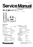
DVD Stereo System
Model No. SA-VK880PU
Product Color: (K)...Black Type
Please file and use this service manual together with the service manual for CR14D, Order No.
PSG0905054AE
TABLE OF CONTENTS
PAGE
1 Safety Precautions----------------------------------------------- 4
1.1. GENERAL GUIDELINES -------------------------------- 4
1.2. Before Use -------------------------------------------------- 4
1.3. Before Repair and Adjustment ------------------------- 4
1.4. Protection Circuitry ---------------------------------------- 5
1.5. Safety Parts Information --------------------------------- 5
2 Warning -------------------------------------------------------------- 6
PAGE
2.1. Prevention of Electrostatic Discharge (ESD)
to Electrostatic Sensitive (ES) Devices---------------6
2.2. Precaution of Laser Diode -------------------------------7
2.3. Service caution based on Legal restrictions --------8
2.4. Handling Precautions for Traverse Unit --------------9
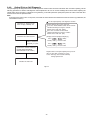
3 Service Navigation --------------------------------------------- 11
3.1. Service Information -------------------------------------- 11
4 Specifications ---------------------------------------------------- 12
© Panasonic Corporation 2009. All rights reserved.
Unauthorized copying and distribution is a violation
of law.
10 Disassembling and Assembling of Traverse Unit --- 88
10.1. Disassembly Procedures ------------------------------ 88
10.2. Assembly Procedures ---------------------------------- 89
11 Service Positions ----------------------------------------------- 90
11.1. Checking and Repairing of Main P.C.B.------------ 90
11.2. Checking and Repairing Panel P.C.B., Deck
P.C.B., Volume P.C.B., Music Port P.C.B. and
Mic P.C.B. ------------------------------------------------- 90
11.3. Checking and Repairing of D-Amp P.C.B.--------- 92
11.4. Checking and Repairing of AC Inlet P.C.B. &
SMPS P.C.B.---------------------------------------------- 94
12 Measurements and Adjustments -------------------------- 96
12.1. Cassette Deck -------------------------------------------- 96
12.2. Tape Speed Adjustment-------------------------------- 96
12.3. Bias Voltage Check ------------------------------------- 97
12.4. Bias Frequency Check -------------------------------- 97
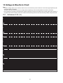
13 Voltage & Waveform Chart ---------------------------------- 98
13.1. DVD Module P.C.B. (1/3) ------------------------------ 98
13.2. DVD Module P.C.B. (2/3) ------------------------------ 99
13.3. DVD Module P.C.B. (3/3) ----------------------------- 100
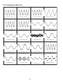
13.4. Main P.C.B. (1/3)---------------------------------------- 101
13.5. Main P.C.B. (2/3)---------------------------------------- 102
13.6. Main P.C.B. (3/3)---------------------------------------- 103
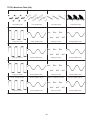
13.7. Panel P.C.B.---------------------------------------------- 104
13.8. Deck P.C.B. ---------------------------------------------- 104
13.9. Mic P.C.B.------------------------------------------------- 104
13.10. D-Amp P.C.B. (1/2) ------------------------------------- 105
13.11. D-Amp P.C.B. (2/2) ------------------------------------- 106
13.12. SMPS P.C.B.--------------------------------------------- 106
13.13. Deck Mechanism P.C.B. ------------------------------ 106
13.14. Volume P.C.B. ------------------------------------------- 107
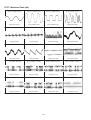
13.15. Waveform Table (1/4)---------------------------------- 108
13.16. Waveform Table (2/4)---------------------------------- 109
13.17. Waveform Table (3/4)---------------------------------- 110
13.18. Waveform Table (4/4)---------------------------------- 111
14 Illustration of ICs, Transistor and Diode --------------- 112
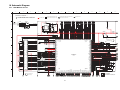
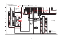
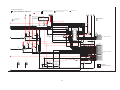
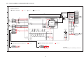
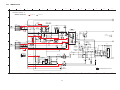
15 Block Diagram -------------------------------------------------- 113
15.1. DVD (Audio)---------------------------------------------- 113
15.2. DVD (Servo) --------------------------------------------- 114
15.3. System Control ------------------------------------------ 115
15.4. Audio------------------------------------------------------- 116
15.5. Video------------------------------------------------------- 117
15.6. Deck-------------------------------------------------------- 118
15.7. D-Amp ----------------------------------------------------- 119
15.8. Power ------------------------------------------------------ 120
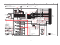
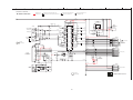
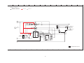
16 Wiring Connection Diagram ------------------------------- 121
17 Schematic Diagram Notes ---------------------------------- 123
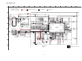
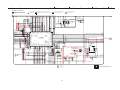
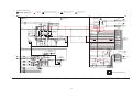
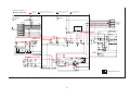
18 Schematic Diagram ------------------------------------------- 125
18.1. DVD Module Circuit ------------------------------------ 125
18.2. Main Circuit----------------------------------------------- 129
18.3. Panel, Side Bar (L) Led & Side Bar (R) Led
Circuit ------------------------------------------------------ 135
18.4. Volume, Music Port, Remote Sensor & Mic
Circuit ------------------------------------------------------ 136
18.5. Deck Circuit ---------------------------------------------- 137
18.6. D-Amp Circuit-------------------------------------------- 138
18.7. SMPS Circuit--------------------------------------------- 140
18.8. USB, Deck Mechanism, AC Inlet & Voltage
Selector Circuit ------------------------------------------ 142
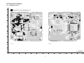
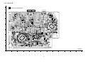
19 Printed Circuit Board----------------------------------------- 143
19.1. DVD Module P.C.B. ------------------------------------ 143
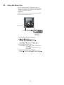
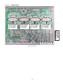
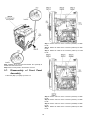
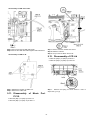
5 Location of Controls and Components------------------ 14
5.1. Main Unit Key Button Operation---------------------- 14
5.2. Remote Control Key Button Operation ------------- 15
5.3. Disc Information ------------------------------------------ 16
5.4. Using the Music Port ------------------------------------ 18
5.5. DivX VIDEO-ON-DEMAND Content ---------------- 19
5.6. USB - Play and Recording ----------------------------- 20
6 Self-Diagnosis and Special Mode Setting -------------- 22
6.1. Service Mode Summary Table ------------------------ 22
6.2. Doctor Mode Table--------------------------------------- 24
6.3. Self-Diagnosis Mode Table --------------------------- 25
6.4. Service Mode Table (For DVD) ----------------------- 26
6.5. DVD Self Diagnostic Function-Error Code--------- 34
6.6. Sales Demonstration Lock Function ---------------- 39
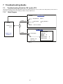
7 Troubleshooting Guide---------------------------------------- 40
7.1. Troubleshooting Guide for F61 and/or F76 -------- 40
7.2. Basic Troubleshooting Guide for Traverse
Unit (DVD Module P.C.B.)------------------------------ 46
8 Service Fixture & Tools --------------------------------------- 47
8.1. Service Tools and Equipment ------------------------- 47
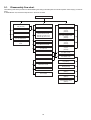
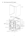
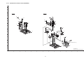
9 Disassembly and Assembly Instructions --------------- 48
9.1. Disassembly flow chart -------------------------------- 50
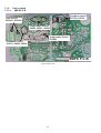
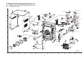
9.2. Main Components and P.C.B. Location ------------ 51
9.3. Disassembly of Top Cabinet--------------------------- 52
9.4. Disassembly of DVD Mechanism Unit
(CR14D) ---------------------------------------------------- 53
9.5. Disassembly of DVD Module P.C.B.----------------- 55
9.6. Disassembly of Rear Panel---------------------------- 55
9.7. Disassembly of Front Panel Assembly ------------- 56
9.8. Disassembly of Mic P.C.B. ----------------------------- 57
9.9. Disassembly of Panel P.C.B., Volume P.C.B.
& Remote Sensor P.C.B. , Side Bar (L) LED
P.C.B. and Side Bar (R) LED P.C.B.----------------- 58
9.10. Disassembly of USB P.C.B. --------------------------- 60
9.11. Disassembly of Music Port P.C.B. ------------------- 61
9.12. Disassembly of CD Lid---------------------------------- 61
9.13. Disassembly of Deck Mechanism Unit ------------- 62
9.14. Disassembly of Deck P.C.B.--------------------------- 63
9.15. Disassembly of Deck Mechanism P.C.B.----------- 63
9.16. Disassembly of Deck Mechanism-------------------- 64
9.17. Disassembly of Cassette Lid -------------------------- 73
9.18. Rectification for Tape Jam Problem ----------------- 73
9.19. Disassembly of D-Amp P.C.B. ------------------------ 74
9.20. Replacement of Audio Digital Power Amp IC
(IC5000) ---------------------------------------------------- 75
9.21. Replacement of Audio Digital Power Amp IC
(IC5200) ---------------------------------------------------- 76
9.22. Replacement of Audio Digital Power Amp IC
(IC5300) ---------------------------------------------------- 76
9.23. Replacement of Audio Digital Power Amp IC
(IC5400) ---------------------------------------------------- 77
9.24. Disassembly of Main P.C.B. --------------------------- 78
9.25. Disassembly of SMPS P.C.B. ------------------------- 79
9.26. Replacement of Switching Regulator IC
(IC5701) ---------------------------------------------------- 80
9.27. Replacement of Rectifier Diode (D5702)----------- 81
9.28. Replacement of Regulator Diode (D5801)--------- 82
9.29. Replacement of Regulator Diode (D5802)--------- 83
9.30. Replacement of Regulator Diode (D5803)--------- 84
9.31. Disassembly of AC Inlet P.C.B. ----------------------- 85
9.32. Disassembly of Voltage Selector P.C.B.------------ 86
2
19.2. Main P.C.B.----------------------------------------------- 144
19.3. Panel, Side Bar (L) Led & Side Bar (R) Led
P.C.B. ------------------------------------------------------ 145
19.4. Volume, Music Port, Remote Sensor, Mic &
USB P.C.B. ----------------------------------------------- 146
19.5. Deck, Deck Mechanism, AC Inlet & Voltage
Selector P.C.B. ------------------------------------------ 147
19.6. D-Amp P.C.B.-------------------------------------------- 148
19.7. SMPS P.C.B.--------------------------------------------- 149
20 Terminal Function of ICs------------------------------------ 151
20.1. IC2801
(RFKWMVK880GC):
IC
MICROPROCESSOR --------------------------------- 151
20.2. IC6601(C0HBB0000057): IC FL Driver ----------- 151
21 Exploded View and Replacement Parts List --------- 153
21.1. Exploded View and Mechanical Replacement
Part List --------------------------------------------------- 153
21.2. Electrical Replacement Part List-------------------- 159
3
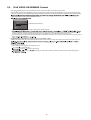
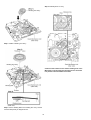
1 Safety Precautions
1.1.
GENERAL GUIDELINES
1. When servicing, observe the original lead dress. If a short circuit is found, replace all parts which have been overheated or
damaged by the short circuit.
2. After servicing, see to it that all the protective devices such as insulation barriers, insulation papers shields are properly
installed.
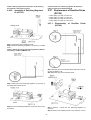
3. After servicing, carry out the following leakage current checks to prevent the customer from being exposed to shock hazards.
1.1.1.
LEAKAGE CURRENT COLD CHECK
1. Unplug the AC cord and connect a jumper between the two prongs on the plug.
2. Measure the resistance value, with an ohmmeter, between the jumpered AC plug and each exposed metallic cabinet part on
the equipment such as screwheads, connectors, control shafts, etc. When the exposed metallic part has a return path to the
chassis, the reading should be between 1MΩ and 5.2MΩ.
When the exposed metal does not have a return path to the chassis, the reading must be
1.1.2.
LEAKAGE CURRENT HOT CHECK
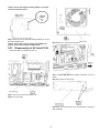
1. Plug the AC cord directly into the AC outlet. Do not use an isolation transformer for this check.
2. Connect a 1.5kΩ, 10 watts resistor, in parallel with a 0.15µF capacitors, between each exposed metallic part on the set and a
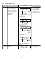
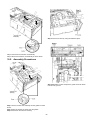
good earth ground such as a water pipe, as shown in Figure 1.
3. Use an AC voltmeter, with 1000 ohms/volt or more sensitivity, to measure the potential across the resistor.
4. Check each exposed metallic part, and measure the voltage at each point.
5. Reverse the AC plug in the AC outlet and repeat each of the above measurements.
6. The potential at any point should not exceed 0.75 volts RMS. A leakage current tester (Simpson Model 229 or equivalent)
may be used to make the hot checks, leakage current must not exceed 1/2 milliamp. In case a measurement is outside of the
limits specified, there is a possibility of a shock hazard, and the equipment should be repaired and rechecked before it is
returned to the customer.
Figure 1
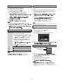
1.2.
Before Use
Be sure to disconnect the mains cord before adjusting the voltage selector.
Use a minus(-) screwdriver to set the voltage selector (on the rear panel) to the voltage setting for the area in which the unit will be
used. (If the power supply in your area is 117V or 120V, set to the “117V or 120V” position.)
Note that this unit will be seriously damaged if this setting is not made correctly. (There is no voltage selector for some countries,
the correct voltage is already set.)
1.3.
Before Repair and Adjustment
Disconnect AC power to discharge unit AC Capacitors as such (C5700, C5701, C5703, C5704, C5705, C5706, C5707) through a
10 Ω, 10 W resistor to ground.
Caution:
DO NOT SHORT-CIRCUIT DIRECTLY (with a screwdriver blade, for instance), as this may destroy solid state devices.
After repairs are completed, restore power gradually using a variac, to avoid overcurrent.
Current consumption at AC 110V~127V, 50/60 Hz at power on (in FM Tuner, no signal at volume minimum) should be ~ 750 mA.
Current consumption at AC 220V~240V, 50/60 Hz at power on (in FM Tuner, no signal at volume minimum) should be ~ 500 mA.
4
1.3.1.
1.4.
Caution for fuse replacement
Protection Circuitry
The protection circuitry may have operated if either of the following conditions are noticed:
• No sound is heard when the power is turned on.
• Sound stops during a performance.
The function of this circuitry is to prevent circuitry damage if, for example, the positive and negative speaker connection wires are
“shorted”, or if speaker systems with an impedance less than the indicated rated impedance of the amplifier are used.
If this occurs, follow the procedure outlines below:
1. Turn off the power.
2. Determine the cause of the problem and correct it.
3. Turn on the power once again after one minute.
Note:
When the protection circuitry functions, the unit will not operate unless the power is first turned off and then on again.
1.5.
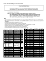
Safety Parts Information
Safety Parts List:
There are special components used in this equipment which are important for safety.
These parts are marked by
in the Schematic Diagrams & Replacement Parts List. It is essential that these critical parts
should be replaced with manufacturer’s specified parts to prevent shock, fire or other hazards. Do not modify the original design
without permission of manufacturer.
Safety
Ref. No.
Part No.
4
REZX0023-1
Part Name & Description
BLK WIRE (AC INLET-SMPS)
5
REZX0024-1
RED WIRE (AC INLET-SMPS)
15
RGRX0070P-E1
REAR PANEL
53
REXX0686-1
WHITE WIRE (VOLT SELECTOR SMPS)
54
REXX0687-1
RED WIRE (VOLT SELECTOR SMPS)
69
RKMX0144A-K
TOP CABINET
340
RD-DDTX004-V
TRAVERSE ASS'Y
A2
K2CQ2CA00007
AC CORD
A3
RQTX0289-M
O/I BOOK (En/Sp)
PCB12
REPX0751G
SMPS P.C.B
(RTL)
PCB13
REPX0751G
AC Inlet P.C.B
(RTL)
DZ5701
ERZV10V511CS
ZNR
S5701
K0ABCA000007
SW AC VOLTAGE SELECTOR
L5703
ELF22V035B
LINE FILTER
T2900
G4D1A0000117
SWITCHING TRANSFORMER
T5701
ETS42BN1A6AD
MAIN TRANSFORMER
T5751
ETS19AB256AG
BACKUP TRANSFORMER
PC5701
B3PBA0000402
PHOTO COUPLER
PC5702
B3PBA0000402
PHOTO COUPLER
PC5720
B3PBA0000402
PHOTO COUPLER
PC5799
B3PBA0000402
PHOTO COUPLER
F1
K5D802BNA005
FUSE
FP2901
K5G401A00008
FUSE PROTECTOR
TH5702
D4CAA2R20001
THERMISTOR
TH5860
D4CC11040013
THERMISTOR
P5701
K2AA2B000017
AC INLET
C5700
F1BAF1020020
1000pF
C5701
F0CAF334A087
0.33uF
C5703
F0C2H1040001
0.1uF
C5704
F1BAF1020020
1000pF
C5705
F1BAF1020020
1000pF
C5706
F1BAF1020020
1000pF
C5707
F1BAF1020020
1000pF
5
500V
Remarks
(RTL)
2 Warning
2.1.
Prevention of Electrostatic Discharge (ESD) to Electrostatic Sensitive
(ES) Devices
Some semiconductor (solid state) devices can be damaged easily by static electricity. Such components commonly are called Electrostatically Sensitive (ES) Devices. Examples of typical ES devices are integrated circuits and some field-effect transistors and
semiconductor "chip" components. The following techniques should be used to help reduce the incidence of component damage
caused by electrostatic discharge (ESD).
1. Immediately before handling any semiconductor component or semiconductor-equipped assembly, drain off any ESD on your
body by touching a known earth ground. Alternatively, obtain and wear a commercially available discharging ESD wrist strap,
which should be removed for potential shock reasons prior to applying power to the unit under test.
2. After removing an electrical assembly equipped with ES devices, place the assembly on a conductive surface such as aluminum foil, to prevent electrostatic charge buildup or exposure of the assembly.
3. Use only a grounded-tip soldering iron to solder or unsolder ES devices.
4. Use only an anti-static solder removal device. Some solder removal devices not classified as “anti-static (ESD protected)” can
generate electrical charge sufficient to damage ES devices.
5. Do not use freon-propelled chemicals. These can generate electrical charges sufficient to damage ES devices.
6. Do not remove a replacement ES device from its protective package until immediately before you are ready to install it. (Most
replacement ES devices are packaged with leads electrically shorted together by conductive foam, aluminum foil or comparable conductive material).
7. Immediately before removing the protective material from the leads of a replacement ES device, touch the protective material
to the chassis or circuit assembly into which the device will be installed.
Caution:
Be sure no power is applied to the chassis or circuit, and observe all other safety precautions.
8. Minimize bodily motions when handling unpackaged replacement ES devices. (Otherwise harmless motion such as the
brushing together of your clothes fabric or the lifting of your foot from a carpeted floor can generate static electricity (ESD) sufficient to damage an ES device).
6
2.2.
Precaution of Laser Diode
Caution:
This product utilizes a laser diode with the unit turned “on”, invisible laser radiation is emitted from the pickup lens.
Wavelength: 655nm (DVD) / 785 nm (CD)
Maximum output radiation power from pickup: 100 µW/VDE
Laser radiation from the pickup unit is safety level, but be sure the followings:
1. Do not disassemble the pickup unit, since radiation from exposed laser diode is dangerous.
2. Do not adjust the variable resistor on the pickup unit. It was already adjusted.
3. Do not look at the focus lens using optical instruments.
4. Recommend not to look at pickup lens for a long time.
7
2.3.
Service caution based on Legal restrictions
2.3.1.
General description about Lead Free Solder (PbF)
The lead free solder has been used in the mounting process of all electrical components on the printed circuit boards used for this
equipment in considering the globally environmental conservation.
The normal solder is the alloy of tin (Sn) and lead (Pb). On the other hand, the lead free solder is the alloy mainly consists of tin
(Sn), silver (Ag) and Copper (Cu), and the melting point of the lead free solder is higher approx.30 degrees C (86°F) more than that
of the normal solder.
Definition of PCB Lead Free Solder being used
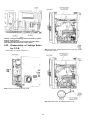
The letter of “PbF” is printed either foil side or components side on the PCB using the lead free solder.
(See right figure)
Service caution for repair work using Lead Free Solder (PbF)
• The lead free solder has to be used when repairing the equipment for which the lead free solder is used.
(Definition: The letter of “PbF” is printed on the PCB using the lead free solder.)
• To put lead free solder, it should be well molten and mixed with the original lead free solder.
• Remove the remaining lead free solder on the PCB cleanly for soldering of the new IC.
• Since the melting point of the lead free solder is higher than that of the normal lead solder, it takes the longer time to melt the
lead free solder.
• Use the soldering iron (more than 70W) equipped with the temperature control after setting the temperature at 350±30 degrees
C (662±86°F).
Recommended Lead Free Solder (Service Parts Route.)
• The following 3 types of lead free solder are available through the service parts route.
RFKZ03D01K-----------(0.3mm 100g Reel)
RFKZ06D01K-----------(0.6mm 100g Reel)
RFKZ10D01K-----------(1.0mm 100g Reel)
Note
* Ingredient: tin (Sn), 96.5%, silver (Ag) 3.0%, Copper (Cu) 0.5%, Cobalt (Co) / Germanium (Ge) 0.1 to 0.3%
8
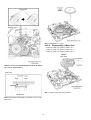
2.4.
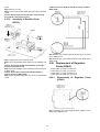
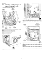
Handling Precautions for Traverse Unit
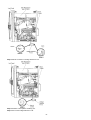
The laser diode in the optical pickup unit may break down due to static electricity of clothes or human body. Special care must be
taken avoid caution to electrostatic breakdown when servicing and handling the laser diode in the traverse unit.
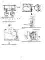
2.4.1.
Cautions to Be Taken in Handling the Optical Pickup Unit
The laser diode in the optical pickup unit may be damaged due to electrostatic discharge generating from clothes or human body.
Special care must be taken avoid caution to electrostatic discharge damage when servicing the laser diode.
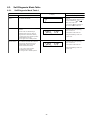
1. Do not give a considerable shock to the optical pickup unit as it has an extremely high-precise structure.
2. To prevent the laser diode from the electrostatic discharge damage, the flexible cable of the optical pickup unit removed
should be short-circuited with a short pin or a clip.
3. The flexible cable may be cut off if an excessive force is applied to it. Use caution when handling the flexible cable.
4. The antistatic FPC is connected to the new optical pickup unit. After replacing the optical pickup unit and connecting the flexible cable, cut off the antistatic FPC.
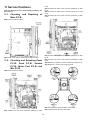
Figure 1
2.4.2.
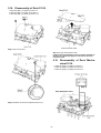
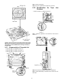
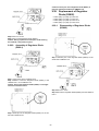
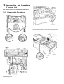
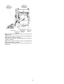
Grounding for electrostatic breakdown prevention
Some devices such as the DVD player use the optical pickup (laser diode) and the optical pickup will be damaged by static electricity in the working environment. Proceed servicing works under the working environment where grounding works is completed.
2.4.2.1.
Worktable grounding
1. Put a conductive material (sheet) or iron sheet on the area where the optical pickup is placed, and ground the sheet.
9
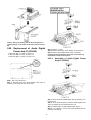
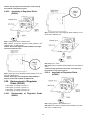
2.4.2.2.
Human body grounding
1. Use the anti-static wrist strap to discharge the static electricity form your body.
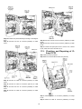
Figure 2
10
3 Service Navigation
3.1.
Service Information
This service manual contains technical information which will allow service personnel’s to understand and service this model.
Please place orders using the parts list and not the drawing reference numbers.
If the circuit is changed or modified, this information will be followed by supplement service manual to be filed with original service
manual.
• DVD Mechanism unit (CR14D):
1) This model uses DVD Mechanism Unit (CR14D).
• Micro-processor & EEPROM IC:
1) The following components are supplied as an assembled part.
- Micro-processor IC, IC2801 (RFKWMVK880GC)
- EEPROM IC, IC2802 (RFKWEVK880GC)
- EEPROM IC, IC8611 (RFKBX0681F-C)
• Speaker system:
1) For information, please refer to original service manual, SB-PF880GC-K, SB-PC880GC-K1, SB-PS880GC-K (Order No.
PSG0906008CE)
• Subwoofer system:
1) For information, please refer to original service manual, SB-WAK780PN-K (Order No. PSG0905028CE).
11
4 Specifications
USB device file system
USB Port power
Bit rate up to
USB Recording
Bit Rate
USB recording speed
Recording file format
Q DISC SECTION
Disc played [8 cm or 12 cm]
Q AMPLIFIER SECTION
RMS Output Power Stereo mode:
Front Ch
125 W per channel (3 Ω), 1 kHz, 10% THD
Surround Ch
125 W per channel (3 Ω), 1 kHz, 10% THD
Center Ch
250 W per channel (6 Ω), 1 kHz, 10% THD
Subwoofer Ch
250 W per channel (3 Ω), 100 Hz, 10% THD
Total RMS Dolby Digital mode
1000 W
power
Q FM/AM TUNER, TERMINALS SECTION
Preset station
FM 30 stations
AM 15 stations
Frequency Modulation (FM)
Frequency range
87.50 to 108.00 MHz (50 kHz
step)
Antenna terminals
75 Ω (unbalanced)
Amplitude Modulation (AM)
Frequency range
522 to 1629 kHz (9 kHz step)
520 to 1630 kHz (10 kHz step)
Music Port (Front) jack
Terminal
Stereo, 3.5 mm jack
Sensitivity
200mV, 4.7kΩ
Phone jack
Terminal
Stereo, 3.5 mm jack
Mic jack
Terminal
Mono, 6.3 mm jack (2 system)
Sensitivity
0.7mV, 1.2kΩ
AUX
Terminal
RCA jack
Q CASSETTE DECK SECTION
Type
Auto reverse
Track system
4-Track, 2 Channel
Heads
Record/playback
Solid permalloy head
Erasure
Double gap ferrite head
Motor
DC servo motor
Recording system
AC bias 100 kHz
Erasing system
AC erase 100 kHz
Tape speed
4.8 cm/s
Overall frequency response (+3, -6 dB) at DECK OUT
Normal
35 Hz to 14 kHz
S/N ratio
50 dB (A-Weighted)
Wow and flutter
0.18 % (WRMS)
Fast forward and rewind time
Approx. 120 seconds with
C-60 cassette tape
Q VIDEO SECTION
Video system
NTSC
Composite video output
Output level
1 Vp-p (75 Ω)
Terminal
Pin jack (1 system)
Component video output
Y output level
1 Vp-p (75 Ω)
0.7 Vp-p (75 Ω)
PB output level
(2) DVD-RAM (DVD-VR, JPEG*4,*7, MP3*2,*7, MPEG4*5,*7, DivX*6,*7)
(3) DVD-R (DVD-Video, DVD-VR, JPEG*4,*7, MP3*2,*7, MPEG4*5,*7,
DivX*6,*7)
(4) DVD-R DL (DVD-Video, DVD-VR)
(5) DVD-RW (DVD-Video, DVD-VR, JPEG*4,*7, MP3*2,*7, MPEG4*5,*7,
DivX*6,*7)
(6) +R/ +RW (Video)
(7) +R DL (Video)
(8) CD,CD-R/RW (CD-DA, Video CD, SVCD*1, MP3*2,*7, WMA*3,*7,
JPEG*4,*7, MPEG4*5,*7, DivX*6,*7)
*1
Conforming to IEC62107
*2
MPEG-1 Layer 3, MPEG-2 Layer 3
*3
Windows Media Audio Ver 9.0 L3
Not compatible with Multiple Bit Rate (MBR)
*4 Exif Ver 2.1 JPEG Baseline files
Picture resolution: between 160 x 120 and 6144 x 4096 pixels (Sub
sampling is 4:0:0, 4:2:0, 4:2:2 or 4:4:4). Extremely long and narrow
pictures may not be displayed.
*5 MPEG4 data recorded with the Panasonic SD multi cameras or
DVD video recorders. Conforming to SD VIDEO specifications (ASF
standard)/ MPEG4 (Simple Profile) video system/ G.726 audio system.
*6
*7
Plays DivX® video.
The total combined maximum number of recognizable audio, picture
and video contents and groups: 4000 audio, picture and video contents and 255 groups (excluding root folder).
Pick up
Wavelength
CD
785 nm
DVD
655 nm
Laser Power
CLASS 1
Audio output (Disc)
Number of channels
5.1 channel (FL, FR, C, SL, SR,
SW)
Q GENERAL
Power supply
AC 110 V to 127 V/220 V to 240 V,
50/60 Hz
Power consumption
132 W
Power consumption in standby mode:
0.4 W (approx.)
Dimensions (W x H x D)
250 mm x 331 mm x 334 mm
Mass
4.9 kg
Operating temperature range
+0 to +40°C
Operating humidity range
35 to 80% RH (no condensation)
Q SYSTEM
Terminal output level
Pin jack (Y: green, PB: blue, PR: red) (1 system)
QUSB SECTION
USB Port
USB standard
Media file format support
128 kbps
1x
MP3 (*.mp3)
(1) DVD (DVD-Video, DivX*6,*7)
0.7 Vp-p (75 Ω)
PR output level
JPEG (*.jpg) (*.jpeg)
DivX (*.divx, *.avi)
MPEG4 (*.asf)
FAT12, FAT16, FAT 32
Max. 500 mA
4 Mbps (DivX)
USB 2.0 full speed
MP3 (*.mp3)
WMA (*.wma)
12
Refer to their respective original service manuals for *1.
Notes:
1. Specifications are subject to changes without notice. Mass and
dimensions are approximate.
2. Total harmonic distortion is measured by the digital spectrum
analyzer.
13
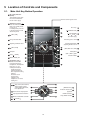
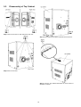
5 Location of Controls and Components
5.1.
Main Unit Key Button Operation
1 AC supply indicator
(AC IN)
This indicator lights when
the unit is connected to
the AC mains supply.
)
Press to switch the unit
from on to standby mode
or vice versa.
In standby mode, the unit
is still consuming a small
amount of power.
Remote control signal sensor
2 Standby/on switch (
11
[ , OPEN/CLOSE] 12
1
12
2
3 [
REC, USB]
Disc trays 11
3
13
[ , EXCHANGE] 13
[1 ] to [5 ]
(disc direct play)
SURROUND
ENHANCER
4
4 Using surround effect
Enhancing bass sound 14
5
6
Selecting Manual EQ, 15
adjusting its BASS level
5 Adjusting subwoofer level
6 [
REC, TAPE]
14
7
15
7 USB port
8
16
9 MUSIC PORT jack
9
17
10 Headphone jack
10
8 Deck [ , OPEN]
[MIN, MIC VOL, MAX] 16
Microphone 17
(MIC 1, MIC 2) jacks
Cassette holder 18
Reduce the volume
level and connect the
headphones. Headphones
plug type: 3.5 mm
stereo (not included).
Avoid listening for
prolonged periods of
time to prevent hearing
damage.
Excessive sound
pressure from
earphones and
headphones can cause
hearing loss.
18
24
19 25 Skip, rewind, fast forward,
Tape Program Sensor,
sound quality adjustment,
time adjustment
19
25
[MANUAL EQ] 24
20
26
21
27
DVD/CD selector and 26
playback
20 USB selector and playback
FM/AM selection 27
21 Tape playback and direction
22 MUSIC PORT/AUX selection
22
23 [ VOLUME ]
23
28
14
Stop, DEMO function 28
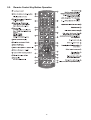
5.2.
Remote Control Key Button Operation
15
5.3.
5.3.1.
Disc Information
Disc Playability (Media)
16
5.3.2.
Tips for Making Data Disc
MP3
This unit does not support ID3 tags.
Sampling frequency and compression rate:
When there are more than eight groups, the eighth group
onwards will be displayed on one vertical line in the menu
screen.
There may be differences in the display order on the menu
screen and computer screen.
This unit cannot play files recorded using packet write.
24 kHz (8 to 160 kbps), 44.1 and 48 kHz (32 to 320 kbps)
32, 44.1 and 48 kHz (32 to 320 kbps)
DVD-RAM
Discs must conform to UDF 2.0.
JPEG
JPEG files taken on a digital camera that conform to DCF
Standard (Design rule for Camera File system) Version 1.0
are displayed. Files that have been altered, edited or saved
with computer picture editing software may not be displayed.
This unit cannot display moving pictures, MOTION JPEG
and other such formats, and still pictures other than JPEG
(Example: TIFF), or play pictures with attached audio.
DVD-R/RW
Discs must conform to UDF bridge (UDF 1.02/ISO9660).
This unit does not support multi-session. Only the default
session is played.
CD-R/RW
Discs must conform to ISO9660 level 1 or 2 (except for
extended formats).
This unit supports multi-session but if there are many
sessions it takes more time for play to start. Keep the number
of sessions to a minimum to avoid this.
Naming folders and files
Example: MP3
Files are treated as contents and folders
are treated as groups on this unit.
At the time of recording, prefix folder and
file names. This should be with numbers
that have an equal number of digits, and
should be done in the order you want to
play them (this may not work at times).
Files must have the extension ( below).
root
MPEG4
You can play MPEG4 data [conforming to SD VIDEO
specifications (ASF standard)/MPEG4 (Simple Profile) video
system/G.726 audio system] recorded with Panasonic SD
multi cameras or DVD video recorders with this unit.
The recording date may differ from that of the actual date.
group
DivX
You can play all versions of DivX video (including DivX 6)
[DivX video system/MP3, Dolby Digital or MPEG audio
system] with standard playback of DivX media files.
Functions added with DivX Ultra are not supported.
DivX files greater than 2 GB or have no index may not be
played properly on this unit.
This unit supports all resolutions up to maximum of
720 x 480 (NTSC)/720 x 576 (PAL).
You can select up to eight types of audio and subtitles on this
unit.
001
track
track
track
group
group
track
track
WMA
track
track
Compatible compression rate:
track
between 48 kbps and 320 kbps.
track
track
You cannot play WMA files that are
copy-protected.
This unit does not support Multiple Bit Rate (MBR).
17
5.4.
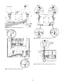
Using the Music Port
You can playback sound from portable audio equipment.
Sound from the speaker may be distorted if the portable audio
equipment s equalizer (if any) is turned on. Turn it off before
you plug into the MUSIC PORT jack.
Preparation
Reduce the volume of the unit and portable audio equipment
before connecting or disconnecting.
MUSIC PORT
Audio cable (not included)
Portable audio
equipment
(not included)
1
Connect the portable audio equipment.
2
Every time you press the button:
FM
3
4
AM
MUSIC PORT
AUX
For listening : Proceed to step 4.
For recording : Press [ REC, TAPE] on the main unit to
start recording.
Press [ REC, USB] on the main unit to
start recording.
Playback the portable audio equipment.
18
5.5.
DivX VIDEO-ON-DEMAND Content
This DivX Certified device must be registered in order to play DivX Video-on-Demand (VOD) content.
First generate the DivX VOD registration code for your device and submit it during the registration process. [Important: DivX VOD
content is protected by a DivX DRM (Digital Rights Management) system that restricts playback to registered DivX Certified devices.
content will not play.] Learn more at www.divx.com/vod.
OTHERS-REGISTRATION (DIVX)
DIVX(R) VIDEO ON DEMAND
YOUR REGISTRATION CODE IS
XXXXXXXX
TO LEARN MORE VISI T
ww w.divx.com/v od
8 alphanumeric characters
SET
RETURN
We recommend that you make a note of this code for future reference.
use this registration code to purchase DivX VOD content. If you use this code to purchase DivX VOD content, and then play the
content on this unit, you will no longer be able to play any content that you purchased using the previous code.
If you purchase DivX VOD content using a registration code different from this unit s code, you will not be able to play this content.
Regarding DivX content that can only be played a set number of times
Some DivX VOD content can only be played a set number of times. When you play this content, the remaining number of plays is
When playing this content
The number of remaining plays is reduced by one if
] or press [SETUP].
]. [Press [ ] (pause) to pause play.]
,
] (skip) or [
,
] (search) etc. and arrive at another content or the start of the content being played.
19
5.6.
USB - Play and Recording
Play
Recording
The USB connectivity enables you to connect and play tracks or
files from USB mass storage class devices.
Typically, USB memory devices. (Bulk only transfer)
Preparation
Before connecting any USB mass storage device to the unit,
ensure that the data stored therein has been backed up.
You can record sound or music tracks from the disc, radio, tape
and other music sources to a USB mass storage device.
Note
A new folder is created each time you perform a recording.
It is not recommended to use a USB extension cable.
The USB device is not recognised by this unit.
1
change once the recording has completed.
All tracks are recorded to .mp3 format.
Do not remove the device or plug out the AC mains lead
while recording, data could be lost.
Voice mixing with CD from microphone cannot be recorded.
Recording indicator blinks while recording in progress.
Connect the USB mass storage device (not included).
Recording indicator
Front panel of
this main unit
USB enabled device
(not included)
Recording of MP3 tracks
2
3
4
Press [ , USB] to begin playback.
Press [MENU] to display the USB menu.
Press [ , ] and then [OK] to select the desired item.
For other operating functions, they are similar as those
Compatible Devices
Devices which are defined as USB mass storage class:
Supported Formats
File name
Still pictures
JPG
Music
MP3 WMA
Video
MPEG4
Connect the USB mass storage device.
4
Press and hold [ , REC] followed by [USB]
(main unit: [ REC, USB]) to start recording.
Insert the disc(s) you want to record.
Press [DVD/CD ] and then [ ] twice.
If the disc contains mixed media.
Recording specific disc(s) or tracks
will be displayed.
File extension
.jpg
.jpeg
.mp3
.wma
5
Press [ ] to stop recording.
.asf
Note
Note
MP3 file needs to be selected before recording can begin. All
files in the current folder will be recorded.
Non-MP3 files will be skipped.
Files in subfolder will be ignored.
*1
It may not be possible to play all the files due to the condition
on how they were created.
*2
For Panasonic D-Snap/DIGA
Note
Maximum number of folders
Maximum number of files
Maximum length of folder name
Maximum length of file name
1
2
3
255
4000
28
28
displayed if volume is adjusted.
CBI (Control/Bulk/Interrupt) is not supported.
Digital Cameras that use PTP protocol or which require
additional program installation when connected to a PC are
not supported.
A device using NTFS file system is not supported.
[Only FAT 12/16/32 (File Allocation Table 12/16/32) file
system is supported].
Depending on the sector size, some files may not work.
It will not operate with Janus enabled MTP (Media Transfer
Protocol) devices.
Only one memory card will be selected when connecting a
multi-port USB card reader. Typically the first memory card
inserted.
20
Track Divide
Recording from audio disc (CDDA)
1 Connect the USB mass storage device
2 Insert the disc(s) you want to record.
3 Press [DVD/CD ] and then [ ] twice.
This function allows you to divide between tracks. You can
choose;
AUTO 5M, track is automatically divided every 5 minutes.
MANUAL, press [OK] during recording to activate track
divide. If the track is not divided manually, every 60 minutes,
track will be divided automatically.
Recording specific disc(s) or tracks
4 Press and hold [ , REC] followed by [USB]
(main unit: [
REC, USB]) to start recording.
1
be displayed.
displayed at FL display.
2 Press [ ,
3 Press [OK] to activate at any time of recording.
5 Press [ ] to stop recording.
Recording track by track from tape.
Skip unnecessary noise by making new track.
Note
Recording is prohibited for disc encoded with copyright
Note
If you press [OK] while using AUTO 5M mode during recording,
the 5 minutes counts will be reset.
When CD MODE is selected;
Erasing the recorded items
This function allows you to erase unwanted tracks quickly and
easily.
1 Press [ , USB] and then [ ] twice.
2 Press [ , ] to select.
3 Press [DEL] and a confirmation page will appear.
Recording from other sources
Tape
1 Connect the USB mass storage device
2 Insert tape into the deck.
3 Search the desired position and then [ ]
Use TPS function for faster search
(
page 24)
mp3-002
Is it OK to delete?
Yes
4 Press and hold [ , REC] followed by
[USB] (main unit: [
recording.
No
REC, USB]) to start
4 Press [ ,
you start recording.
5 Press [ ] to stop recording.
Erasing items in order (Playback Menu)
Radio
Music
Port
AUX
Tune to the required station.
Using the Music Port
PLAYBACK MENU
MP3, WMA, JPEG
DivX, MPEG4
Using an external unit
Note
This unit will analyse the USB device before recording.
The time taken to
start recording may vary depending on the device used.
AUDIO/PICTURE
VIDEO
OK
1 Press [ ,
and press [OK]. When either one is selected, other file will
become invisible and cannot be deleted.
Press [DEL] to delete.
2
3 Repeat step 2 until all files are deleted.
4 Re-insert the device to continue.
Note
locked.
Folders containing subfolders or unsupported files cannot be
deleted.
21
6 Self-Diagnosis and Special Mode Setting
This unit is equipped with features od self-diagnosis & special mode setting for checking the function & reliability.
Special Note: Checking of the reliability (ageing) & changer operation must be carry out to ensure good working condition
in unit.
6.1.
6.1.1.
Service Mode Summary Table
Doctor Mode Summary Table
Main unit buttons
[
]
Remote control unit buttons
[4], [7]
(In Doctor Mode)
[ODISC]
6.1.2.
Application
Enter into doctor mode.
Changer check
Self-Diagnosis Mode Summary Table
Main buttons
[STOP] +
[ /FF/
]
(In self-diagnostic
mode) + [ ]
Remote control unit buttons
-
Servicing the mechanism unit.
(In self-diagnostic
mode) + [ ]
In Self-diagnosis
mode
-
Servicing the traverse unit.
6.1.3.
Note
(Refer to the section “6.2. Doctor Mode
Table” for more information.)
Application
Entering into self-diagnostic mode.
[2]
Reliability 2 (Cycle)
[3]
Reliability 3 (Combi)
Note
(Refer to the section
“6.3.1.
Self-Diagnosis
Mode Table 1” for more
information.)
(Refer to the section
“6.3.2.
Self-Diagnosis
Mode Table 2” for more
information.)
Service Mode Summary Table (For DVD)
The service modes can be activated by pressing various button combination on the main unit and remote control unit.
Below is the summary for the various modes for checking:
Main buttons
[STOP]
Remote control unit buttons
[0]
[5]
[PAUSE]
[FUNCTIONS]
[3]
[6]
[7]
[8]
[DISC]
[ENTER]
Application
Error code display.
Jitter checking.
Initial setting of laser drive current.
DVD laser drive current check.
CD laser drive current check.
Region display and mode.
Micro-processor firmware version check.
Initialization of the player (factory setting is restored).
Used after replacement of Micro-processor (DV5 LSI) IC, FLASH
ROM IC (IC8651), EEPROM IC (IC8611) and DVD Module
P.C.B.
DVD Module P.C.B. firmware version check.
CPPM/CPRM keys check.
DVD Module P.C.B. reset.
Timer 1 check.
Timer 1 reset.
Timer 2 check.
Timer 2 reset.
22
Note
(Refer to the section
“6.4.1. Service Mode
Table 1” for more information.)
(Refer to the section
“6.4.2. Service Mode
Table 2” for more information.)
(Refer to the section
“6.4.3. Service Mode
Table 3“ for more information.)
(Refer to the section
“6.4.4. Service Mode
Table 4“ for more information.)
(Refer to the section
“6.4.5. Service Mode
Table 5“ for more information.)
Note:
An error code will be canceled if a power supply is turned OFF.
*1: CPPM is the copy guard function beforehand written in the disk for protection of copyrights.
*2: CEC is the consumer electronic control used for high-level user control of HDMI-connected devices.
*3: HDCP is the specification developed to control digital audio & video contents transmission for DVI or HDMI connections.
23
6.2.
Doctor Mode Table
Key Operation
Item
FL Display
Mode Name
Doctor Mode
Description
To enter into Doctor Mode for checking
of variuos items and displaying
EEPROM and firmware version.
Front Key
(Display 1)
Note: The micro-processor version
as shown is an example. It will be
revise when there is an update.
FL Display sequence:
Display 1 2.
In CD Mode:
1. Press [ -DEMO] button
on main unit follow by [4]
and [7] on remote control.
Opecon
Version
EEPROM Checksum
(if applicable)
To exist, press [ok] button on
remote control or press
[ /I, POWER] button on main
unit or remote control.
1. The check Sum of EPPROM and firmware
version will be display.
* ROM correction.
* Firmware Version No:
checksum: (Condition 1):
No Correction
Firmware
Point Data
Version (DEC)
If there is no EEPROM Correction.
checksum: (Condition 2):
Checksum
Firmware
value (HEX)
Version (DEC) applicable
when the
EEPROM IC
is installed
If the EEPROM version matches, checksum
[YYYY] is displayed.
checksum: (Condition 3):
Firmware
Version (DEC)
Firmware
different from
set
If the version of the EEPROM does not
match or not working properly [NG] is
displayed
CR14D
Inspection
To check the function operation of
mechanism unit
In Doctor mode:
1. Press [ DISC] button
on remote control.
To exist, press any key
24
6.3.
Self-Diagnosis Mode Table
6.3.1.
Self-Diagnosis Mode Table 1
Item
Mode Name
Self-Diagnostic
Mode
FL Display
Key Operation
Description
Front Key
To enter into self-diagnostic checking
for CR14D mechanism.
In DVD/CD mode (ensure no disc is
inserted):
Press and hold [STOP] button for five
seconds, followed by [ /FF/
]
button on the main unit.
To exit, press [ /l, AC IN] button on
main unit or remote control unit.
Service Mode 1
To unlock the mechanism unit for
service.
In self-diagnostic mode, press [1]
button on main unit.
In this mode, the disassembly of
CR14D can be carry out. (Refer to
original service manual for CR14D)
To exit, power off the main unit
Press [EXCHANGE] on main unit
for error code.
1. All trays are set to "STOCK" position.
2. Mechanism set to tray 1.
3. Cam gear set to "HOME" position.
Service Mode 2
To unlock the traverse unit for service.
In self-diagnostic mode, press [2]
button on main unit.
In this mode, traverse unit can be
disassembled. (Refer to original
service manual for CR14D)
To exit, power off the main unit
Press [EXCHANGE] on main unit
for error code.
1. Tray 5 set to "Play" position.
2. Mechanism set to tray 5.
3. Cam gear set to "HOME" position.
25
6.3.2.
Self-Diagnosis Mode Table 2
Item
Mode Name
Reliability
2
(Traverse Cycle
Test)
FL Display
Description
To determine playability operation.
Key Operation
Front Key
Display 1
In self-diagnostic mode, press [2]
button on remote control.
To exit, press [ /l ] button on the
main unit or remote control unit.
Display 2
The counter will
increment by one.
When reach 99999
will change to 00000
Reliability
3
(Combi Cycle
Test)
The combine test for both load &
traverse cycle test.
Display 1
In self-diagnostic mode, press [3]
button on remote control.
To exit, press [ /l ] button on the
main unit or remote control unit.
Display 2
The counter will
increment by one.
When reach 99999
will change to 00000
6.4.
Service Mode Table (For DVD)
By pressing various button combinations on the main unit and remote control unit, you can activate the various service modes for
checking.
Special Note:
• Due to the limitations of the no. characters that can be shown on the FL Display, the “FL Display” button on the remote control
unit can be used to show the two display pages. (Display 1 / Display 2).
• Refer to Section 5.2 for the section on “Remote Control Key Buttons Operations”.
26
6.4.1.
Service Mode Table 1
Item
Mode Name
Jitter check
Key Operation
FL Display
Description
Jitter check.
Jitter rate is measured and displayed.
Measurement is repeatedly done in
the cycle of one second. Read error
counter starts from zero upon mode
setting.
When target block data failed to be
read out, the counter advances by one
increment. When the failure is caused
by minor error, it may be corrected
when retried to enable successful
reading.
In this case, the counter advances by
one. When the error persists even
after retry, the counter may jump by
two or more.
Front Key
In STOP (no disc) mode,
press [STOP] button on the
main unit, and [5] button on
the remote control unit.
Press [STOP] button to
exit.
(Display 1)
Jitter Check
Jitter Rate
Mode
Jitter rate is shown in decimal notation to
one place of decimal.
Focus drive value is shown in hexadecimal
notation.
(Display 2)
Press [FL Display] on
remote control unit for next
page (FL Display).
FL Display sequence:
Display 1 2.
Lead
Error
Counter
Error code
display
Error code check
The latest error code stored in the
EEPROM IC is displayed.
Note: Refer to "Section 8.4 DVD Self
Diagnostic Function-Error Code" for
more detailed information on the error
codes.
Initial setting
of laser drive
current
Focus Drive
Value
Initial setting of laser drive current.
Initial current value for the DVD laser
and CD laser is separately saved in
the EEPROM IC.
FL Display sequence:
Display 1 2.
U/H/F
Error code (play_err) is expressed in the
following convention.
Error code = 0 x DAXX is expressed:
DVDnn U12
Error code = 0 x DBXX is expressed:
DVDnn H12
Error code = 0 x DXXX is expressed:
DVDnn F123
Error code = 0 x 0000 is expressed:
DVDnn F--* "xx" denotes the error code
(Display 1)
Laser Current
Measurement
Mode
The value denotes the current in decimal
notation.
In STOP (no disc) mode,
press [STOP] button on the
main unit, and [0] button on
the remote control unit. * With
pointing of cursor up and
down on display.
Cancelled automatically
5 seconds later.
To exit, press [POWER]
button on main unit or
remote control.
In STOP (no disc) mode,
press [STOP] button on the
main unit, and [PAUSE]
button on the remote
control unit.
Cancelled automatically
5 seconds later.
(Display 2)
Press [FL Display] on
remote control unit for next
page (FL Display) on values
of laser drive current.
CD
Laser
Identify
as LDO
mode
DVD Laser
The above example shows the initial
current is XXXmA and YYYmA for CD
laser and DVD laser respectively when
the laser is switched on.
27
6.4.2.
Service Mode Table 2
Key Operation
Item
Mode Name
DVD laser
drive current
measurement
FL Display
Description
DVD laser drive current measurement.
DVD laser drive current is measured
and the result is displayed together
with the initial value stored in the
EEPROM IC.
After the measurement, DVD laser
emission is kept on. It is turned off
when POWER key is switched off.
FL Display sequence:
Display 1 2.
(Display 1)
DVD laser current
measurement mode
The value denotes the current in decimal
notation.
(Display 2)
Front Key
In STOP (no disc) mode,
press [STOP] button on the
main unit, and
[FUNCTIONS] button on
the remote control unit.
Cancelled automatically
5 seconds later.
Press [FL Display] on
remote control unit for next
page (FL Display) on values
of dvd drive current.
DVD Identify as
DVD
Laser LDD mode
Laser
Initial Value Value
The above example shows the initial
current is XXXmA and the measured
value is YYYmA.
CD laser drive
current
measurement
CD laser drive current measurement.
CD laser drive current is measured
and the result is displayed together
with the initial value stored in the
EEPROM IC.
After the measurement, CD laser
emission is kept on. It is turned off
when POWER key is switched off.
FL Display sequence:
Display 1 2.
(Display 1)
CD Laser Current
Measurement Mode
In STOP (no disc) mode,
press [STOP] button on
the main unit, and [3]
button on the remote
control unit.
Cancelled automatically
5 seconds later.
The value denotes the current in decimal
notation.
(Display 2)
Press [FL Display] on
remote control unit for next
page. (FL Display)
CD Laser
CD
Laser Initial Value
Value
The above example shows the initial current
is XXXmA and the measured value is
YYYmA.
28
6.4.3.
Service Mode Table 3
Item
Mode Name
Micro-processor
firmware version
display &
EEPROM
checksum
display.
Key Operation
FL Display
Description
Front Key
Micro-processor firmware version
display & EEPROM checksum display.
EEPROM checksum is only available
due to existence of EEPROM IC.
(Display 1)
Note: Condition 1/2/3 shows the state
of EEPROM IC. It is indicated in
Display 2.
(Display 2)
In STOP (no disc)
mode, press [STOP]
button on the main unit,
and [7] button on the
remote control unit.
Cancelled automatically
5 seconds later.
FL Display sequence:
Display 1 2 3.
Opecon
Version
(Condition1)
EEPROM
Checksum
(If applicable,
refer below.)
If the version of the EEPROM does not match,
[NG] is displayed.
(Condition 2)
(a) If there is NO EEPROM header string
OR
(b) If there is no EEPROM (no data is received
by Micro-processor), [NO] is displayed.
(Condition 3)
If the EEPROM version matches, checksum
[YYYY] is displayed.
(Display 3)
Press [FL Display] button on
remote control unit for next
page. (FL Display)
Initialization
mode
Initialization.
User settings are cancelled and player
is initialized to factory setting.
It is necessary when after replacement
of Micro-processor (DV5 LSI) IC,
FLASH ROM IC (IC8651), EEPROM
IC (IC8611) & DVD Module P.C.B.
In STOP (no disc)
mode, press [STOP]
button on the main unit,
and [ 10] button on the
remote control unit.
Cancelled automatically
5 seconds later.
Region display
Region code display, TV broadcasting
system & the model no. information.
In STOP (no disc)
mode, press [STOP]
button on the main unit,
and [6] button on the
remote control unit.
Cancelled automatically
5 seconds later.
Model
No.
Information
N: NTSC / 6: PAL60
N: no PAL / P: PAL
Note: Refer to Fig. 8.1 for "Video
Design Information".
Region No.: 0-8
29
Model Series
P, PC, PX
Country Region
Region TV Broadcasting
Product
Signal System Region Display
(Default)
(Default)
OSD
Default
Code
System
USA, Canada, PX
1
NTSC
NTSC (*A)
1PN
English
Japan
2
NTSC
NTSC (*A)
2PN
Japanese
OSD Menu Language
English, Spanish,
Canadian, French
(S)
Japanese, English
English, French, German,
2
Europe
EP
PAL
PAL (*C)
2P6
English
Spanish, Polish, Russian,
Czech, Hungarian
English, French, German,
2
Europe
EB, EG
PAL
2P6
PAL (*C)
English
Italian, Spanish, Polish,
Swedish, Dutch
English, French, German,
Middle East
GC, GS
2
PAL
PAL (*C)
2P6
English
Spanish, Polish, Russian,
Czech, Hungarian
GA, GD,
GT, GJ
Hong Kong,
South East Asia,
Thailand,
Korea, Taiwan
PAL
3
NTSC (*B)
3PN
English
English, Traditional Chinese
NTSC
English, French, German,
New Zealand,
GN
4
PAL
PAL (*C)
4P6
English
Italian, Spanish, Polish,
Australia
Swedish, Dutch
PN, PH, PU,
PR
Central/South/
4
NTSC
NTSC (*D)
4PN
English
English, Spanish, French,
Brazilian Portuguese
Latin America
English, French, German,
EE
5
CIS
SECAM
PAL (*C)
5P6
English
6PN
English
Spanish, Polish, Russian,
Czech, Hungarian
GK
6
China
PAL
NTSC (*B)
NTSC (*B)
NTSC (*A)
PAL (*C)
Output
Source
Output
Source
Screen Saver
NTSC
Screen Saver
NTSC
Screen Saver
NTSC disc
NTSC
Source
NTSC disc
NTSC (default)
NTSC (DVD-A/VCD)
NTSC (*D)
NTSC disc
Output
PAL
PAL60 (default)
PAL60
PAL (DVD-V)
PAL disc
English, Simplified Chinese
PAL disc
PAL
NTSC
PAL disc
PAL
Explanation of Display
Source
Output
Screen Saver
NTSC
NTSC disc
NTSC
PAL disc
NTSC
Individual Model Code
N: If NTSC disc is played, NTSC output.
6: If NTSC disc is played, PAL60 output.
Can play PAL disc
Region code
Figure 1 Video Design Information
30
6.4.4.
Service Mode Table 4
Item
Mode Name
DVD Module
P.C.B. firmware
version display
FL Display
Description
Front Key
DVD Module P.C.B. firmware version
is displayed on the FL Display.
The firmware version can be updated
using recovery disc.
System
controller
version
Destination
System controller
generation
Region No.: 0-8
Note: It is necessary to check for
firmware version before carrying out
the version up using the disc.
CPPM/CRM
Keys Check
CPPM/CRM refers to the Content
Protection for Recordable Media and
Pre-Recorded Media. It displays the
existence of the keys as "1" or "0".
OK: Existing of keys.
NG: Non existing of keys.
0: NG 0: NG
1: OK 1: OK
DVD Module
P.C.B. Reset
Key Operation
In STOP (no disc)
mode, press [STOP]
button on the main unit,
and [8] button on the
remote control unit.
Cancelled automatically
5 seconds later.
In STOP (no disc)
mode, press [STOP]
button on the main unit,
and [DISC] button on the
remote control unit.
Cancelled automatically
5 seconds later.
While in initialization
mode, press & hold
[STOP] button on the main
unit, follow by [OK] button
on the remote control unit.
Cancelled automatically
5 seconds later.
To reset DVD Module P.C.B.
This process is used when the DVD
Module P.C.B. or FLASH ROM
IC is replaced with a new one.
31
6.4.5.
Service Mode Table 5
Item
Mode Name
Timer 1 check
Key Operation
FL Display
Description
Timer 1 check
Laser operation timer is measured
separately for DVD laser and CD laser.
(Display 1)
FL Display sequence:
Display 1 2.
DVD laser usage time
Front Key
In STOP (no disc)
mode, press [STOP]
button on the main unit,
and [ ] button on the
remote control unit.
Cancelled automatically
5 seconds later.
Shown to the above is DVD laser usage
time, and to the below is CD laser usage
time.
Time is shown in 4 digits of decimal notation
in a unit of 10 hours.
"0000" will follow "9999". (DVD laser)
(Display 2)
Press [FL Display] button for
next page of FL Display.
CD laser usage time
Time is shown in 4 digits of decimal notation
in a unit of 10 hours.
"0000" will follow "9999". (CD laser)
Timer 1 reset
Timer 2 check
Timer 2 reset
Timer 1 reset
Laser operation timer of both DVD
laser and CD laser is reset all at once.
Time is shown in 4 digits of decimal notation
in a unit of 10 hours.
It will clear to "0000" upon reset.
While displaying Timer 1
data, press [STOP] button
on the main unit, and [ ]
button on the remote
control unit.
Cancelled automatically
5 seconds later
Time is shown in 5 digits of decimal notation in
a unit of 1 hour.
"00000" will follow "99999".
In STOP (no disc)
mode, press [STOP]
button on the main unit,
and [ ] button on the
remote control unit.
Cancelled automatically
5 seconds later.
Timer 2 check
Spindle motor operation timer
Timer 2 reset
Spindle motor operation timer
Time is shown in 5 digits of decimal notation in
a unit of 1 hour.
It will be cleared to "00000" upon activating
this.
32
While displaying Timer 2
data, press [STOP] button
on the main unit, and [ ]
button on the remote
control unit.
Cancelled automatically
5 seconds later.
6.4.6.
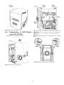
Optical Pick-up Self-Diagnosis
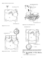
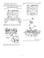
The optical pickup self-diagnosis function and tilt adjustment check function have been included in this unit. When repairing, use the
following procedure for effective self-diagnosis and tilt adjustment. Be sure to use the self-diagnosis function before replacing the
optical pickup when "NO DISC" is displayed. As a guideline, you should replace the optical pickup when the value of the laser drive
current is more than the specified value.
Note:
Press the power button to turn on the power, and check the value within three minutes before the unit warms up. (Otherwise, the
result will be incorrect.)
Use the optical pickup self-diagnosis function.
"NO DISC" is displayed, unit
does not play smoothly, etc.
Check the laser drive current.
Method: With no disc in the main unit:
Press the "FUNCTIONS" button on the remote
control unit while pressing the "STOP"
button on the main unit. (DVD)
Press the "3" button on the remote
control unit while pressing the "STOP"
button on the main unit. (CD)
[Display content (display1/display2)]
LDD /
(DVD)
Factory setting
Value is more than
37 (DVD), 41 (CD).
Replace the traverse unit.
(Refer to the section "OPTICAL
PICKUP REPLACEMENT
PROCEDURE" in this Guide.)
LDC /
Factory setting
Present value
(CD)
Present value
Replace with a new optical pickup if the present
value is more than 37 (DVD), 41 (CD).
Cause: Damage due to static electricity
during replacement.
Initialize the main unit.
Figure 2
33
6.5.
DVD Self Diagnostic Function-Error Code
6.5.1.
Error
DVD Module Error Code Table
Diagnosis Contents
Description of error
Automatic FL Display
Remarks
Code
U702 HDMI/DVI I2C
communication error
The communication error of I2C when
Press [
connecting it with HDMI/DVI. For
unit for next error.
STOP] on main
instance, when EDID information to which
information on the TV set side has been
described cannot be read, it is generated.
U703 HDMI/DVI attestation
error
When attestation (HDCP) with the TV
Press [
side fails when connecting it with
unit for next error.
STOP] on main
HDMI/DVI, it is generated.
U704 HDMI/DVI SRM
Riborcerar
It is generated at the equipment to which
Press [
the TV set is Riborced when connecting it
unit for next error.
STOP] on main
with HDMI/DVI.
U705 HDMI/DVI SRM disk
falsification check
error
It is generated at the time of it is time
Press [
when illegal the SRM data of the
unit for next error.
STOP] on main
reproducing disk (verify error), when
connecting it with HDMI/DVI.
F740 HDMI device key
F893 FLASH ROM IC data
falsification error
F894 EEPROM IC
abnormality error
I2C error when writing HDMI Key device
Press [
into transmitter.
unit for next error.
STOP] on main
Firmware error, DV5.0 LSI IC (IC8651)
Press [
error.
unit for next error.
STOP] on main
When failing in the access to EEPROM
Press [
IC located in the DVD Module P.C.B.
unit for next error.
STOP] on main
(IC8611).
F895 Language area
Firmware version agreement check for
Press [
abnormal
factory preset setting failure prevention.
unit for next error.
Incomplete initialization after writing of
Press [
new firmware (Factory preset setting
unit for next error.
F897 Initialization
error
STOP] on main
STOP] on main
failure prevention)
F899 The communication
Unsuitable combination of number of
Press [
specification
system com and panel com used.
unit for next error.
disagreement
(Frimware)
between
micro-processor
34
STOP] on main
6.5.2.
DVD Mechanism Unit (CR14D) Error Code Table
Error
Diagnosis Contents
Description of error
Code
H01 Tray loading error
The tray opening and closing is
abnormal. CLOSE and OPEN of the
tray cannot be carried out properly.
Loading motor error, DV5 LSI IC
(IC8001) error.
H02 Spindle servo error
The spindle servo/motor is abnormal.
The FG pulse is abnormal. CLV servo
error.
Automatic FL Display
Remarks
Press [ STOP] on
main unit for next error.
(OPEN time: OPEN
CLOSE
OPEN
H01 at CLOSE: CLOSE
OPEN
CLOSE
H01)
Press [ STOP] on
main unit for next error.
H03 Traverse servo error The traverse is abnormal. (Traverse
servo, DV5 LSI IC (IC8001), TRV
motor error.)
Press [ STOP] on
main unit for next error.
H04 Tracking servo error Tracking coil NG (OPU unit
abnormal), DV5 LSI IC (IC8001)
error.
H05 Seek time out error It is not possible to access the disc.
TOC cannot read. Abnormal disc etc.
Pickup abnormal or disk is dirty.
(TRV motor error, DV5 LSI IC
(IC8001) error.)
H07 Driver IC thermal
The spindle motor is abnormal. (short
shut down
between brushes)
Press [ STOP] on
main unit for next error.
Press [ STOP] on
main unit for next error.
Press [ STOP] on
main unit for next error.
H15 Disc tray open
detection switch
failure
The disc tray cannot be opened & it
closes spontaneously.
Press [ STOP] on
main unit for next error.
H16 Disc tray close
detection switch
failure
The disc tray cannot be closed & it
opens spontaneously.
Press [ STOP] on
main unit for next error.
U11 Focus servo error
Focus coil, FE signal error.
Press [ STOP] on
main unit for next error.
(Unfinalized DVD-R
is likely to beocme U11.)
F500 DSC error
DV5 LSI IC (IC8001) stops in the
occurance of servo error (startup,
focus error, etc)
Press [ STOP] on
main unit for next error.
F506 Invalid media
Disc is flipped over, TOC unreadable,
incompatible disc.
Press [ STOP] on
main unit for next error.
F620 OPU unit
abnormality
temperature
Laser protection at high temperature.
Press [ STOP] on
main unit for next error.
F621 OPU unit
circuitry
temperature
Laser protection at circuit failure.
Press [ STOP] on
main unit for next error.
U15 Unfinalized DVD-R
35
6.5.3.
Error
Power Supply & Digital Amplifier Error Code Table
Diagnosis Contents
Description of error
Automatic FL Display
Remarks
Code
F61 The abnormalities
In normal operation, when DCDET2 goes
Press [
in an output or power
to "L" (Low) (Not during POWER OFF
unit for next error.
STOP] on main
supply circuit of
condition), F61 appears on FLDisplay
POWER AMP
for 1 second and PCONT goes to
"L" (Low).This is due to speaker output
has DC voltage or fan is not working.
F76 Abnormality in the
output voltage of
In normal operation when DCDET1 is
Press [
detected "L" (Low) for two consecutive
unit for next error.
stabilized power
times, F76 is displayed on FL for
supply
1 second and after that PCONT will be
STOP] on main
turned to "L" (Low). This is due to any of
the DC voltages (+9V, +7V, -7V, +5V,
+5.3V etc.) C22 not available.
6.5.4.
Error
USB Error Code Table
Diagnosis Contents
Description of error
Automatic FL Display
Remarks
Code
F650 USB device: Devices
other than mass
Devices other than the mass storage
Press [
STOP] on main
class are connected.
unit for next error.
storage
F651 USB device: Non-Full
Speed Device
The device that the transfer rate did not
Press [
correspond to Full Speed was
unit for next error.
STOP] on main
connected.
F652 USB device:
Interface NG
The device in the interface (subclass)
Press [
outside correspondence was connected.
unit for next error.
STOP] on main
(correspondence interface)
001b: Reduced Block Commands (RBC)
010b: SFF-8020i. MMC-2 (ATAPI)
110b: SCSI transparent command set.
F655 USB device:
Overcurrent detection
The overcurrent of 500mA or more was
Press [
detected in VDD USB, and the USB
unit for next error.
device driver function was intercepted.
(To intercept the current.)
36
STOP] on main
6.5.5.
DVD Changer Mechanism Unit (CR14D) Error Code Table
Error Code Diagnosis Contents Description of error
LOAD
Load operation faulty The load operation cannot
complete when time out
occurs.
Automatic FL Display
Remarks
For DVD Mechanism unit (CR14D).
Press [EXCHANGE] on main unit for
next error.
UNLD
Unload operation
faulty
The unload operation
cannot complete when time
out occurs.
For DVD Mechanism unit (CR14D).
Press [EXCHANGE] on main unit for
next error.
UP
Exchange open
operation faulty
The exchange open
operation cannot complete
when time out
occurs.
For DVD Mechanism unit (CR14D).
Press [EXCHANGE] on main unit for
next error.
DOWN
Down operation faulty The down operation cannot
complete when time out
occurs.
For DVD Mechanism unit (CR14D).
Press [EXCHANGE] on main unit for
next error.
OPEN
Open operation faulty The open operation cannot
complete when time out
occurs.
For DVD Mechanism unit (CR14D).
Press [EXCHANGE] on main unit for
next error.
CLOSE
Close operation faulty The open operation cannot
complete when time out
occurs.
For DVD Mechanism unit (CR14D).
Press [EXCHANGE] on main unit for
next error.
MODEL
Mode change to
updown operation
faulty
For DVD Mechanism unit (CR14D).
Press [EXCHANGE] on main unit for
next error.
The mode change to
updown operation cannot
complete when time out
occurs. It changes to
up/down.
Error Code Diagnosis Contents
MODEH
Mode change to
horizontal operation
faulty
Description of error
The mode change to
horizontal operation cannot
complete when time out
occurs.
INITIALIZE Initialize operation
faulty
The initialize operation
cannot complete.
Automatic FL Display
Remarks
For DVD Mechanism unit (CR14D).
Press [EXCHANGE] on main unit for
next error.
For DVD Mechanism unit (CR14D).
Press [EXCHANGE] on main unit for
next error.
37
6.5.6.
Deck Mechanism Error Code Table
38
6.6.
Sales Demonstration Lock Function
This function prevents discs from being lost when the unit is used for sales demonstrations by disabling the disc eject function.
"LOCKED" is displayed on the unit, and ordinary operation is disabled.
6.6.1.
Setting
• Prohibiting removal of disc
1. Select the DVD/CD function.
2. At POWER ON condition, press and hold down the
button and the power button on the main unit for at least three seconds. (The message, “LOCKED” appears when the function is activated.)
Note:
OPEN/CLOSE button is invalid and the main unit displays “LOCKED” while the lock function mode is entered.
• Prohibiting operation of selector and disc
1. Select the DVD/CD function.
2. At POWER ON condition, press and hold down the button and the power button on the main unit for at least three seconds. (The message, “LOCKED” appears when the function is activated.)
Note:
The following buttons are invalid and the main unit displays “LOCKED” while the lock function mode is entered.
Main unit
Remote controller unit
6.6.2.
OPEN/CLOSE,
/-TUNE MODE/—FM MODE, SELECTOR,
iPod/USB, FM/EXT-IN, NUMERIC KEYS 0~9,
PLAY/SLEEP, MUTING
,
,
/
,
/
,
,
/
,
,
/
, RETURN, FUNCTIONS, FL DIS-
Cancellation
The lock can be cancelled by the same procedure as used in setting. ("UNLOCKED" is displayed on cancellation. Disconnecting the
power cable from power outlet does not cancel the lock.)
39
7 Troubleshooting Guide
7.1.
Troubleshooting Guide for F61 and/or F76
This section illustrates the checking procedures when upon detecting the error of “F61” and/or “F76” after power up of the unit. It is
for purpose of troubleshooting and checking in SMPS, D-Amp & Main P.C.B.
7.1.1.
Block Diagram
SMPS P.C.B.
SYS6V
Temperature
DCDET 2
30V Detect
Detect
( 30V_SENSE )
SYS6V
+ 18V Fan Detect
DCDET1/2
(F61)
D -AMP P.C.B.
MAIN P.C.B.
(MICRO-P)
DCDET 1
FAN Detect
Speaker Out
DC Detect
Figure 1
40
SUBWOOFER
CENTER
FRONT - R
FRONT - L
SURROUND - R
SURROUND - L
7.1.2.
Troubleshooting Guide
Symptom
FL display blinking with
abnormal segment when
power ON the set or "F61"
Checking Items
Check the soldering of the SMPS
P. C.B.
x Is there any solder crack at area
(Q5860,Q5861, Q5862,TH5860)
x Check all the supply line
First Power ON Display
immediate show "F61".
Power ON for a while then
only trigger "F61".
(Symptom always happen)
30V
x Is there any solderability at area
of feedback circuit
x Check feedback circuit (IC5801,
Q5802, D5806, PC5720, D5725)
Check Speaker output by using
multi-meter,
x If there is a DC Voltage around
30V
x Check Output IC (Pin 10 &
14) which have DC Voltage at
Speaker output short to
Vdd/Vss
x If shorted that means D-Amp
damage already.
Check the fan connection &
feedback loop:
x If the fan not proper connected,
"F61" will trigger when the
volume increase.
x If the fan is not working, check
for fan circuit.
Check the soldering of the SMPS
P. C.B.
x Is there any solder crack at area
(Q5860,Q5861, Q5862,TH5860)
x Check all the supply line
30V
x +18V at ZJ2701 (Pin 8 & 9)
Power ON for a while and
then trigger "F76"
Check all supply voltages as
follows:
Step 1: Check for supply voltages
from SMPS P. C.B to Main
P. C.B at pin 2,5,8,9 of CN5802.
If there are supply voltages,
proceed to Step 2.
If no voltages detected, check wire
connection and circuitry connection
from SMPS P. C.B.
Step 2: Check if there is supply
voltages for Vp, FL1 & FL2
CN2807
x If there is supply voltages of
+2.7V at CN2801, Pin 19 & 17
+5V at CN2801, Pin 26
+5V at CN2807, Pin 5
x If there is supply voltages of
9V at CN6001
41
Repair Items
Tou ch-up the solder crack area/
Change the defective parts.
x Q5860,Q5861,Q5862,TH5860
(Tem perature Detect)
Remarks
SMPS
P. C.B.
Refer to
Figure 2
x QR5801 & QR5802 ( 30V
Detect)
x Tou ch-up the necessary areas
x IC5801, Q5802, D5806,
PC5720, D5725
Change the defective parts.
D-AMP IC:
IC5000/IC5200/IC5300/IC5400
P/N = C1BA00000492
D-AMP
P. C.B.
Refer to
Figure 3
For Configuration
Refer to Figure 5
Re-connect the Fan to CN2810
Fan circuit: Q2942, Q2943,
Q2948 & Q2949
Main
P. C.B.
Refer to
Figure 4
Touch-up the solder crack area/
Change the defective parts.
D-Amp
P. C.B.
x Q5860,Q5861,Q5862,TH5860
(Tem perature Detect)
x QR5801 & QR5802 ( 30V
Detect)
Feedback Circuit: IC5801, Q5802
PC5720, D5725, D5806
Check and change the possible
defective parts.
Refer to
Figure 3
Main
P. C.B.
Refer to
Figure 4
x FP2901 (Fuse Protector),
T2900, D2901
x IC4000 (Switching Regulator IC)
& related regulator circuit
components
7.1.3.
7.1.3.1.
Part Location
SMPS P.C.B.
Feedback circuit:
PC5720, D5725
+30V Detect:
QR5801, QR5802,
Temperature Detect:
Q5860, Q5681, Q5862
Temperature Detect:
TH5860
Feedback Circuit:
IC5801, Q5802, D5806
SMPS P.C.B.
Figure 2 SMPS P.C.B.
42
D-Amp P.C.B.
Audio Digital
Power Amp
IC: IC5400
Audio Digital
Power Amp
IC: IC5000
Audio Digital
Power Amp
IC: IC5200
Audio Digital
Power Amp
IC: IC5300
SPEAKER
OUTPUT
7.1.3.2.
D-Amp P.C.B.
Figure 3 D-Amp P.C.B.
43
7.1.3.3.
Main P.C.B.
Transistor:
Q2942, Q2943,
Q2948, Q2949
(Fan Circuit)
Connector: CN2807
Fuse Protector:
FP2091
Switching
Regulator
IC: IC4000
T2900,
D2901
Figure 4 Main P.C.B.
44
7.1.3.4.
D-Amp IC Configuration
VK880PU-K
Pin (10)
Sub-Woofer +
Pin (14)
Sub-Woofer -
Pin (10)
Center +
Pin (14)
Center-
Pin (10)
Front Right
Pin (14)
Front Left
Pin (10)
Surround
Right
Pin (14)
Surround
Left
IC5300
IC5200
IC5000
IC5400
Figure 5 D-Amp IC Configuration
45
7.2.
Basic Troubleshooting Guide for Traverse Unit (DVD Module P.C.B.)
Problems
1) Distorted picture or
abnormal sound is head
during the initialization
Checking Points
Checking components
a) Check SDRAM address, data
bus, CLK and other control signals
waveform
IC8051
b) Check video signals (Y,C)
LB8301, R8321, R8323,
LB8302, R8325, R8327
c) Check audio DAC circuitry
IC8420 (Pin 3, 10 to 11)
* Compare the above with
OK condition DVD Module
P.C.B
LB8421, LB8422
*Check for solder short and/or
component missing/damaged
a) Check motor driver circuitry
(+5V)
IC8251 Pin 8, 21
b) Check laser drive circuitry
(Voltages & current)
Q8551, Q8552 (For DVD),
Q8561, Q8562 (For CD)
c) Check LSI IC connection to
motor drive circuitry
* Compare the above with OK
condition DVD Module P.C.B.
IC8001 Pin 66, 67
IC8251 Pin 15 to 16, 17, 18
* Check for solder short and/or
component missing/damaged
a) Check connection from
DVD Module to Traverse unit
FP8251
b) Check motor driver circuitry on
the voltages and control signals
* Compare the above with
OK condition DVD Module P.C.B.
IC8251
6) Cannot read the disc but
spindle motor is spinning
- Cannot read CD/DVD
a) Check laser drive circuitry
(voltages and current)
- Check CD Laser Drive
- Check DVD Laser Drive
* Check voltages and LD current
and compare with OK condition
DVD Module P.C.B.
Q8551, Q8552, LB8551
(For DVD Laser Drive current)
Q8561, Q8562, LB8561
(For CD Laser Drive current)
7) Block Noise during play
a) Check SDRAM IC address and
data bus signal
IC8051
8) Jitter out of specification
a) Check LD current
b) Check OPU (Change to other
unit and confirmed operating
condition)
OPU Unit (Traverse unit), FPC
connection (FP8531 & FP8251)
2) No TOC/Long TOC
3) Disc not spinning
4) Traverse not moving
5) Traverse and spindle
abnormal movement
46
* Check for solder short and/or
component damaged
8 Service Fixture & Tools
8.1.
Service Tools and Equipment
Prepare service tools before process service position.
Service Tools
Remarks
Main P.C.B. (CN2808) - D-Amp P.C.B. (CN5050)
Main P.C.B. (ZJ2701) - SMPS P.C.B. (CN5802)
SMPS P.C.B. (H5801) - D-Amp P.C.B. (CN5500)
REEX0930 (17P FFC)
REXX0680 (11P Cable)
REXX0683 (8P Cable)
47
9 Disassembly and Assembly Instructions
“ATTENTION SERVICER”
Be careful when disassembling and servicing.
Some chassis components may have sharp edges.
Special Note:
1. This section describes the disassembly procedures for all the major printed circuit boards and main components.
2. Before the disassembly process was carried out, do take special note that all safety precautions are to be carried
out.
(Ensure that no AC power supply is connected during disassembling.)
3. For assembly after operation checks or replacement, reverse the respective procedures.
Special reassembly procedures are described only when required.
4. Do take note of the locators on each printed circuit board during reassembling procedures.
5. The Switch Regulator IC may have high temperature after prolonged use.
6. Use caution when removing the top cabinet and avoid touching heat sinks located in the unit.
7. Select items from the following index when checks or replacement are required.
• Disassembly of Top Cabinet
• Disassembly of DVD Mechanism Unit (CR14D)
• Disassembly of Rear Panel
• Disassembly of Front Panel Assembly
• Disassembly of Panel P.C.B., Volume P.C.B., Remote Sensor P.C.B., Side Bar (L/R) LED P.C.B.
• Disassembly of Mic P.C.B.
• Disassembly of USB P.C.B.
• Disassembly of Music Port P.C.B.
• Disassembly of CD Lid
• Disassembly of Deck Mechanism Unit
• Disassembly of Deck P.C.B.
• Disassembly of Deck Mechanism
• Disassembly of Deck Mechanism P.C.B.
• Disassembly of Cassette Lid
• Rectification for Tape Jam Problem
• Disassembly of D-Amp P.C.B.
• Replacement of Audio Digital Power Amp IC (IC5000)
• Replacement of Audio Digital Power Amp IC (IC5200)
• Replacement of Audio Digital Power Amp IC (IC5300)
• Replacement of Audio Digital Power Amp IC (IC5400)
• Disassembly of Main P.C.B.
• Disassembly of SMPS P.C.B.
• Replacement for Switching Regulator IC (IC5701)
• Replacement for Switching Regulator Diode (D5702)
• Replacement for Regulator Diode (D5801)
• Replacement for Regulator Diode (D5802)
• Replacement for Regulator Diode (D5803)
• Disassembly of AC Inlet P.C.B.
• Disassembly of Voltage Selector P.C.B.
• Disassembly of DVD Module P.C.B.
• Disassembling and Assembling of Traverse Unit.
Below shown is part no. of different screws types used:
48
49
9.1.
Disassembly flow chart
The following chart is the procedure for disassembling the casing and inside parts for internal inspection when carrying out the servicing.
To assemble the unit, reverse the steps shown in the chart as below.
9.3. Top Cabinet
9.4 DVD Mechanism
Unit (CR14D)
9.5 DVD Module P.C.B.
9.6 Rear Panel
9.7 Front Panel Assembly
9.19 D-Amp P.C.B.
9.8 Mic P.C.B.
9.20 Audio Digital Power
Amp IC
(IC5000)
9.9 Panel, Volume,
Remote Sensor P.C.B.
Side Bar (L) LED P.C.B.
Side Bar (R) LED P.C.B.
9.31 AC Inlet P.C.B.
9.10 USB P.C.B.
9.32 Voltage Selector
P.C.B.
9.11 Music Port P.C.B.
9.21 Audio Digital Power
Amp IC
(IC5200)
9.22 Audio Digital Power
Amp IC
(IC5300)
9.12 CD Lid
9.23 Audio Digital Power
Amp IC
(IC5400)
9.13 Deck Mechanism Unit
9.24 Main P.C.B.
9.17 Cassette Lid
9.25 SMPS P.C.B.
9.14 Deck P.C.B.
9.15 Deck
Mechanism P.C.B.
9.26 Switching Regulator
IC (IC5701)
9.27 Switching Regulator
Diode (D5702)
9.16 Deck Mechanism
9.18 Rectification for Tape
Jam Problem
9.28 Regulator Diode
(D5801)
9.29 Regulator Diode
(D5802)
9.30 Regulator Diode
(D5803)
50
9.2.
Main Components and P.C.B. Location
51
9.3.
Disassembly of Top Cabinet
Step 1 Remove 3 screws on each side of the main unit.
Step 3 Lift the sides of top cabinet outwards as arrow shown.
Step 2 Remove 5 screws.
Step 4 Push the top cabinet backwards as arrow shown to
release the catches.
52
Step 5 Remove the top cabinet.
9.4.
Step 2 Detach 50P FFC cable at the connector (CN2801) on
Main P.C.B.
Step 3 Detach 11P FFC cable at the connector (CN2805) on
Main P.C.B.
Step 4 Detach 5P cable at the connector (CN1113) on USB
P.C.B.
Disassembly of DVD Mechanism Unit (CR14D)
• Follow the (Step 1) to (Step 5) of Item 9.3
Step 5 Release the claws outwards on both sides.
Step 1 Remove 1 screw at rear panel.
53
Caution: During assembling, ensure the claws are fully
catched.
Caution: During assembling, ensure that the DVD Mechanism Unit (CR14D) is seated properly at the locator.
Step 6 Release the DVD Mechanism Unit (CR14D) from the
catches and locators.
Step 7 Lift up DVD Mechanism Unit (CR14D) in the direction of
arrow.
Step 8 Detach 7P FFC at the connector (FP8251).
Step 9 Detach 26P FFC at the connector (FP8531).
• Disassembly of Mecha Chassis
54
Step 10 Remove 2 screws.
Step 11 Remove Mecha Chassis as arrow shown.
9.5.
Disassembly of DVD Module
P.C.B.
• Follow the (Step 1) to (Step 5) of Item 9.3
• Follow the (Step 1) to (Step 9) of Item 9.4
Step 1 Remove 10 screws at rear panel.
Step 2 Remove 1 screw at rear panel.
Step 3 Release 2 catches from the each side of the rear panel.
Step 1 Remove 3 screws.
Step 2 Remove the shield plate unit.
Step 3 Remove DVD Module P.C.B..
9.6.
Disassembly of Rear Panel
• Follow the (Step 1) to (Step 5) of Item 9.3
55
Step 1 Detach 27P FFC at the connector (CN2807) on Main
P.C.B..
Step 2 Detach 2P cable at the connector (CN2813) on Main
P.C.B..
Step 3 Detach 5P cable at the connector (CN1113) on USB
P.C.B..
Step 3 Slightly lift up the DVD Mechanism Unit (CR14D) to
release from the two locators.
Step 4 Remove rear panel in the direction of arrow.
9.7.
Disassembly of Front Panel
Assembly
• Follow the (Step 1) to (Step 5) of Item 9.3
Step 4
P.C.B..
Step 5
P.C.B..
Step 6
P.C.B..
Step 7
P.C.B.
56
Detach 10P FFC at the connector (CN2752) on Main
Detach 12P FFC at the connector (CN2751) on Main
Detach 10P FFC at the connector (CN2806) on Main
Detach 2P cable at the connector (CN2812) on Main
Caution: Do not exert strong force when releasing the tabs.
Step 8 Release the claws on both sides.
Step 9 Release catches at both side.
Caution: During assembling, ensure that both claws and
catches are fully catched.
Step 11 Remove 1 screw to remove ground wire.
Step 12 Remove front panel assembly in the direction of arrow.
9.8.
Disassembly of Mic P.C.B.
• Follow the (Step 1) to (Step 5) of Item 9.3
• Follow the (Step 1) to (Step 12) of Item 9.7
Step 1 Remove Mic knob.
Step 10 Release the tabs at the bottom.
57
Step 2 Detach 7P cable at the connector (CN6702) on Mic
P.C.B..
Step 2 Detach 7P cable at the connector (CN6702) on Mic
P.C.B..
Step 3 Remove 1 screw on Mic P.C.B..
Step 4 Remove the Mic P.C.B..
9.9.
Disassembly of Panel P.C.B.,
Volume P.C.B. & Remote Sensor P.C.B. , Side Bar (L) LED
P.C.B. and Side Bar (R) LED
P.C.B.
• Follow the (Step 1) to (Step 5) of Item 9.3
• Follow the (Step 1) to (Step 12) of Item 9.7
• Follow the (Step 2) of Item 9.8
Step 3 Remove 9 screws at Panel P.C.B..
Step 1 Remove volume knob.
58
Step 4 Remove 2 screws on Volume P.C.B..
Step 6 Release 6 catches at Volume P.C.B..
Step 7 Release 2 catches at Remote Sensor P.C.B..
Step 5 Release 2 catches at Panel P.C.B..
59
Caution: During assembling, ensure that the diodes shown
on Volume P.C.B. are in upright position.
Step 8 Lift up the Panel P.C.B., Volume P.C.B. & Remote Sensor P.C.B. altogether as arrow shown.
• Disassembly of Side Bar (L) Led P.C.B. and Side Bar (R)
P.C.B.
Step 9 Detach Side Bar (L) P.C.B at the connector (CN6014)
on Panel P.C.B..
Step 10 Detach Side Bar (R) P.C.B at the connector (CN6012)
on Panel P.C.B..
Step 11 Remove the Side Bar (L) P.C.B. and Side Bar (R)
P.C.B..
Caution: During assembling, ensure that Dynamic Bass
Button is seated properly.
9.10. Disassembly of USB P.C.B.
• Follow the (Step 1) to (Step 5) of Item 9.3
• Follow the (Step 1) to (Step 12) of Item 9.7
60
• Disassembly of USB Jack holder.
Step 1 Remove 2 screws at USB Jack holder.
Step 2 Remove the USB Jack holder together with USB P.C.B..
Step 1 Remove 2 screws at Music Port P.C.B..
Step 2 Release 2 catches.
Step 3 Lift up to remove Music Port P.C.B..
• Disassembly of USB P.C.B..
9.12. Disassembly of CD Lid
• Follow the (Step 1) to (Step 5) of Item 9.3
• Follow the (Step 1) to (Step 12) of Item 9.7
Step 3 Release the catches at USB P.C.B..
Step 4 Remove the USB P.C.B..
9.11. Disassembly
P.C.B.
of
Music
Step 1 Remove the spring as arrow shown in order of
sequences (1) to (3).
Port
• Follow the (Step 1) to (Step 5) of Item 9.3
• Follow the (Step 1) to (Step 12) of Item 9.7
61
Caution: During assembling, please ensure that the spring
is assembly at right position.
Step 2 Remove CD Lid as arrow shown.
9.13. Disassembly of Deck Mechanism Unit
• Follow the (Step 1) to (Step 5) of Item 9.3
• Follow the (Step 1) to (Step 12) of Item 9.7
Step 2 Push the lever upward as arrow shown to open the cassette lid.
Step 3 Remove Deck Mechanism Unit in the direction of arrow.
Step 1 Remove 4 screws at Deck Mechanism Unit.
62
9.14. Disassembly of Deck P.C.B.
• Follow the (Step 1) to (Step 5) of Item 9.3
• Follow the (Step 1) to (Step 12) of Item 9.7
• Follow the (Step 1) to (Step 3) of Item 9.13
Step 1 Remove 2 screws.
Step 3 Lift up & remove Deck P.C.B..
Caution: During assembling, ensure connector (CP1301) at
Deck P.C.B. is seated properly & connected to the head
connector cable.
9.15. Disassembly of Deck Mechanism P.C.B.
• Follow the (Step 1) to (Step 5) of Item 9.3
• Follow the (Step 1) to (Step 12) of Item 9.7
• Follow the (Step 1) to (Step 3) of Item 9.13
Step 2 Desolder 2P wire at the Capstan Motor Ass’y.
63
Step 1 Desolder the plunger terminals.
Step 4 Remove Deck Mechanism P.C.B..
Step 2 Remove 1 screw.
Caution: During assembling, ensure that the Deck Mechanism P.C.B. is seated properly with the guide of the locators.
Step 3 Release 4 catches.
9.16. Disassembly of Deck Mechanism
• Follow the (Step 1) to (Step 5) of Item 9.3
64
• Follow the (Step 1) to (Step 12) of Item 9.7
• Follow the (Step 1) to (Step 3) of Item 9.13
• Follow the (Step 1) to (Step 3) of Item 9.14
Caution: Avoid exerting strong force as it may damage the
FFC.
9.16.1. Replacement of Pinch Roller Ass’y
and Head Block Sub Ass’y
Step 5 Remove 2 screws.
Step 1 Release catch to remove the Pinch Roller (F) Assy.
Step 2 Release catch to remove the Pinch Roller (R) Assy.
Step 6 Remove Head Block Sub Ass’y as arrow shown.
Step 3 Release the catches at the side of head connector.
Step 4 Detach the head connector as arrow shown.
65
9.16.2. Replacement of Capstan
Ass’y and Capstan Belt ‘A’
Motor
• Follow the (Step 3) to (Step 4) of item 9.16.1.
- Disassembly of Capstan Motor Ass’y and Capstan Belt ‘A’
Step 2 Lift up to remove the Sub-Chassis Ass’y.
Step 1 Remove 3 screws.
Step 3 Remove 2 screws to remove Capstan Motor Ass’y.
Caution: Support Capstan Motor Ass’y by hand to prevent
it from falling during removal and assembly of Capstan
Motor Ass’y.
66
Step 4 Remove Capstan Belt ‘A’.
- Assembly of Capstan Motor Ass’y and Capstan Belt ‘A’
Step 1 Coil Capstan Belt ‘A’ to Flywheel ‘F’ Ass’y, Flywheel ‘L’
and the 2 bosses temporarily as diagram shown.
Caution: Keep Capstan Belt ‘A’ away from grease during
assembly of Capstan Belt ‘A’.
67
Step 2 Fit the Capstan Motor Ass’y to the Sub-Chassis Ass’y.
Caution: Ensure it seats properly.
Step 3 Fix the Capstan Motor Ass’y to the Sub-Chassis Ass’y
by 2 screws.
Step 5 Fix 3 screws.
Step 6 Release Capstan Belt ‘A’ to the pulley of Capstan Motor
Ass’y as diagram shown.
9.16.3. Replacement of Winding Belt
• Follow the (Step 3) to (Step 4) of item 9.16.1.
• Follow the (Step 1) to (Step 4) of item 9.16.2.
Step 4 Install the Sub-Chassis Ass’y to the Deck Mechanism
Unit.
Caution: Ensure the Sub-Chassis Ass’y seats properly on
the bosses.
- Disassembly of Winding Belt
68
Step 1 Release 2 catches and press the tip of the Winding
Lever downwards.
Step 2 Remove Flywheel ‘L’ Ass’y.
Step 3 Remove the Winding Lever.
Step 4 Remove the Thrust Spring.
Step 5 Remove the Winding Arm Ass’y.
Step 6 Remove the Flywheel ‘F’ Ass’y.
Step 7 Remove the Winding Belt.
Caution: Keep Thrust Spring in a safe place for assembling
purpose.
- Assembly of Winding Belt
69
Step 3 Install Flywheel ‘F’ Ass’y.
Step 1 Install the Winding Arm Ass’y.
Caution: Ensure that the boss and the marking hole of the
Main Gear are positioned such that they form a horizontal
line parallel to the Deck Mechanism Unit.
Step 2 Coil the Winding Belt to the Winding Arm Ass’y and the
2 bosses temporarily as diagram shown.
70
Step 4 Install the Thrust Spring.
Step 5 Install the Winding Lever.
Caution 2: Ensure that the Winding Lever is firmly inserted
and properly catched on the tape side as diagram shown.
Caution 1: Ensure that the Winding Arm Ass’y is pulled
towards to the right as arrow shown to enable full insertion
of the Winding Lever. The Winding Lever must be seated
on the Main Gear as diagram shown.
71
Step 7 Install Flywheel ‘L’ Ass’y.
9.16.4. Disassembly of Main Gear
• Follow the (Step 3) to (Step 4) of item 9.16.1.
• Follow the (Step 1) to (Step 4) of item 9.16.2.
• Follow the (Step 1) to (Step 6) of item 9.16.3.
Caution 3: Ensure that the Winding Belt is above the Winding Lever as diagram shown.
Step 1 : Remove Main Gear using tweezers.
Step 6 Release the Winding Belt on Flywheel ‘F’ Ass’y as diagram shown.
72
Step 1 Remove the spring.
Step 2 Push the cassette lid in the direction of arrows.
9.18. Rectification
Problem
for
Tape
Jam
• Follow the (Step 1) to (Step 5) of Item 9.3
Step 1 Rotate the flywheel F in the direction of the arrow to
remove it.
Caution : Ensure that the boss and the marking hole of the
Main Gear are positioned such that they form a horizontal
line parallel to the Deck Mechanism during assembly of
the Main Gear.
9.17. Disassembly of Cassette Lid
• Follow the (Step 1) to (Step 5) of Item 9.3
• Follow the (Step 1) to (Step 12) of Item 9.7
• Follow the (Step 1) to (Step 3) of Item 9.13
Step 2 Push the lever upward and open the cassette lid.
Note: Follow Disassembly of Cassette Lid to remove the cassette tape.
73
9.19. Disassembly of D-Amp P.C.B.
• Follow the (Step 1) to (Step 5) of Item 9.3
• Follow the (Step 1) to (Step 6) of Item 9.4
Step 1 Remove 4 screws at the rear panel.
Step 5 Lift up the D-Amp P.C.B. together with the inner chassis
assembly as arrow shown.
Step 6 Remove 2 screws on D-Amp P.C.B..
Step 2 Detach 17P FFC at the connector (CN5050) on D-Amp
P.C.B..
Step 3 Detach 8P cable at the connector (CN5500) on D-Amp
P.C.B..
Step 4 Remove 2 screws at D-Amp P.C.B. Inner chassis
assembly.
Step 7 Lift up D-Amp P.C.B. as arrow shown.
74
Caution: During assembling, ensure the D-Amp P.C.B. is
seated properly on the locator of the Inner chassis assembly.
9.20. Replacement of Audio Digital
Power Amp IC (IC5000)
Step 3 Remove 1 screw.
Step 4 Remove TR Spring in the direction of arrow shown.
Step 5 Remove Audio Digital Power Amp IC (IC5000).
Caution: During replacement of the part, avoid touching
the heatsink, it may lead to injuries.
• Follow the (Step 1) to (Step 5) of Item 9.3
• Follow the (Step 1) to (Step 7) of Item 9.4
• Follow the (Step 1) to (Step 7) of Item 9.19
9.20.1. Assembly of Audio Digital Power
Amp IC (IC5000)
Step 1 Flip over D-Amp P.C.B..
Step 2 Desolder pins of the Audio Digital Power Amp IC
(IC5000) on the solder side of D-Amp P.C.B..
Step 1 Mount the Audio Digital Power Amp IC (IC5000) on to
D-Amp P.C.B..
Step 2 Screw back TR Spring to hold the Audio Digital Power
Amp IC (IC5000) onto the Heatsink Power Unit.
Step 3 Solder the pins of Audio Digital Power Amp IC.
Step 4 Use a blower to remove the minute particles after the
screwing of TR Spring.
75
Caution: During replacement of the part, avoid touching
the heatsink, it may lead to injuries.
Caution: Ensure pins of the Audio Digital Power Amp IC
(IC5000) are properly seated and soldered on D-Amp
P.C.B..
9.21.1. Assembly of Audio Digital Power
Amp IC (IC5200)
9.21. Replacement of Audio Digital
Power Amp IC (IC5200)
• Follow the (Step 1) to (Step 5) of Item 9.3
• Follow the (Step 1) to (Step 7) of Item 9.4
• Follow the (Step 1) to (Step 7) of Item 9.19
Step 1 Flip over D-Amp P.C.B..
Step 2 Desolder pins of the Audio Digital Power Amp IC
(IC5200) on the solder side of D-Amp P.C.B..
Step 1 Mount the Audio Digital Power Amp IC (IC5200) on to
D-Amp P.C.B..
Step 2 Screw back TR Spring to hold the Audio Digital Power
Amp IC (IC5200) onto the Heatsink Power Unit.
Step 3 Solder the pins of Audio Digital Power Amp IC.
Step 4 Use a blower to remove the minute particles after the
screwing of TR Spring.
Caution: Ensure pins of the Audio Digital Power Amp IC
(IC5200) are properly seated and soldered on D-Amp
P.C.B..
9.22. Replacement of Audio Digital
Power Amp IC (IC5300)
• Follow the (Step 1) to (Step 5) of Item 9.3
• Follow the (Step 1) to (Step 7) of Item 9.4
• Follow the (Step 1) to (Step 7) of Item 9.19
Step 3 Remove 1 screw.
Step 4 Remove TR Spring in the direction of arrow shown.
Step 5 Remove Audio Digital Power Amp IC (IC5200) from the
heat sink unit.
Step 1 Flip over D-Amp P.C.B..
Step 2 Desolder pins of the Audio Digital Power Amp IC
(IC5300) on the solder side of D-Amp P.C.B..
76
Caution: Ensure pins of the Audio Digital Power Amp IC
(IC5300) are properly seated and soldered on D-Amp
P.C.B..
9.23. Replacement of Audio Digital
Power Amp IC (IC5400)
• Follow the (Step 1) to (Step 5) of Item 9.3
• Follow the (Step 1) to (Step 7) of Item 9.4
• Follow the (Step 1) to (Step 7) of Item 9.19
Step 1 Flip over D-Amp P.C.B..
Step 2 Desolder pins of the Audio Digital Power Amp IC
(IC5400) on the solder side of D-Amp P.C.B..
Step 3 Remove 1 screw.
Step 4 Remove TR Spring in the direction of arrow shown.
Step 5 Remove Audio Digital Power Amp IC (IC5300).
Caution: During replacement of the part, avoid touching
the heatsink, it may lead to injuries.
9.22.1. Assembly of Audio Digital Power
Amp IC (IC5300)
Step 3 Remove 1 screw.
Step 4 Remove TR Spring in the direction of arrow shown.
Step 5 Remove Audio Digital Power Amp IC (IC5400) from the
heat sink unit.
Step 1 Mount the Audio Digital Power Amp IC (IC5300) on to
D-Amp P.C.B..
Step 2 Screw back TR Spring to hold the Audio Digital Power
Amp IC (IC5300) onto the Heatsink Power Unit.
Step 3 Solder the pins of Audio Digital Power Amp IC.
Step 4 Use a blower to remove the minute particles after the
screwing of TR Spring.
77
Caution: During replacement of the part, avoid touching
the heatsink, it may lead to injuries.
9.23.1. Assembly of Audio Digital Power
Amp IC (IC5400)
Step 1 Detach 11P cable at connector (CN5802) on SMPS
P.C.B..
Step 2 Detach 2P cable at connector (CN2810) on SMPS
P.C.B..
Step 1 Mount the Audio Digital Power Amp IC (IC5400) on to
D-Amp P.C.B..
Step 2 Screw back TR Spring to hold the Audio Digital Power
Amp IC (IC5400) onto the Heatsink Power Unit.
Step 3 Solder the pins of Audio Digital Power Amp IC.
Step 4 Use a blower to remove the minute particles after the
screwing of TR Spring.
Caution: Ensure pins of the Audio Digital Power Amp IC
(IC5400) are properly seated and soldered on D-Amp
P.C.B..
9.24. Disassembly of Main P.C.B.
•
•
•
•
Follow the (Step 1) to (Step 5) of Item 9.3
Follow the (Step 1) to (Step 7) of Item 9.4
Follow the (Step 1) to (Step 7) of Item 9.7
Follow the (Step 1) to (Step 5) of Item 9.19
Step 3 Remove 2 screws on Main P.C.B..
78
Step 4 Remove 3 screws at rear panel.
Step 1 Detach 11P cable at the connector (CN5802) on SMPS
P.C.B..
Step 5 Remove Main P.C.B. according to the arrow shown.
9.25. Disassembly of SMPS P.C.B.
• Follow the (Step 1) to (Step 5) of Item 9.3
• Follow the (Step 1) to (Step 7) of Item 9.4
• Follow the (Step 1) to (Step 5) of Item 9.19
Step 2 Remove 4 screws on SMPS P.C.B..
Step 3 Lift up the SMPS P.C.B. as arrow shown.
79
Caution: During assembling, ensure that SMPS P.C.B. is
seated properly at the locators.
9.26. Replacement of Switching Regulator IC (IC5701)
•
•
•
•
Follow (Step 1) to (Step 5) of Item 9.3
Follow (Step 1) to (Step 7) of Item 9.4
Follow (Step 1) to (Step 5) of Item 9.19
Follow (Step 1) to (Step 5) of Item 9.25
9.26.1. Disassembly of Switching Regulator IC (IC5701)
Step 4 Flip the SMPS P.C.B. and desolder 2 wires pins (red
and black).
• For GA/GS only
Step 1 Desolder pins of the switching regulator IC (IC5701) on
the solder side of SMPS P.C.B.
Step 5 Desolder 2 wires pins (blue and white).
Step 2 Remove 1 screw from the Switch Regulator IC
(IC5701).
Step 3 Remove the Switch Regulator IC (IC5701).
80
Caution: During replacement of the part, avoid touching
the heatsink, it may lead to injuries.
Caution: Ensure the switching regulator IC (IC5701) is
tightly screwed to the Heatsink Unit B.
9.26.2. Assembly of Switching Regulator
IC (IC5701)
9.27. Replacement of Rectifier Diode
(D5702)
•
•
•
•
Follow (Step 1) to (Step 5) of Item 9.3
Follow (Step 1) to (Step 7) of Item 9.4
Follow (Step 1) to (Step 5) of Item 9.19
Follow (Step 1) to (Step 5) of Item 9.25
9.27.1. Disassembly
(D5702)
of
Rectifier
Diode
Step 1 Apply grease to the Heatsink Unit B.
Step 2 Mount the Switching Regulator IC (IC5701) on to SMPS
P.C.B..
Caution: Ensure pins of the switching regulator IC (IC5701)
are properly seated on SMPS P.C.B.
Step 1 Desolder pins of the Rectifier Diode (D5702) on the solder side of SMPS P.C.B..
Step 2 Desolder pins of the Heatsink Unit B.
Step 3 Solder pins of the Switching Regulator IC (IC5701) on
the solder side of SMPS P.C.B..
Step 4 Screw the Switching Regulator IC (IC5701) to the Heatsink Unit B.
Step 3 Remove 1 screw from the Switching Regulator IC
(IC5701).
Step 4 Remove the Heatsink Unit B in the direction of arrow
81
Caution: Ensure the Heatsink Unit B is properly seated on
SMPS P.C.B.
shown.
Step 5 Remove 1 screw.
Step 6 Remove the Rectifier Diode (D5702) from the Heatsink
Unit B.
Caution: During replacement of the part, avoid touching
the heatsink, it may lead to injuries.
9.27.2. Assembly of Rectifier Diode
(D5702)
Step 5 Solder pins of the Rectifier Diode (D5702) on the solder
side of SMPS P.C.B..
Step 6 Solder pins of the Heatsink Unit B on the solder side of
SMPS P.C.B..
Step 1 Apply grease to the Heatsink Unit B.
Step 2 Screw the Rectifier Diode (D5702) to the Heatsink Unit
B..
Caution: Ensure the Rectifier Diode (D5702) is well tightened to the Heatsink Unit B.
Step 3 Mount the Heatsink Unit B & Rectifier Diode (D5702) on
to SMPS P.C.B..
Caution: Ensure pins of the Rectifier Diode (D5702) is
properly seated on SMPS P.C.B..
Step 4 Screw the Switch Regulator IC (IC5701) to the Heatsink
Unit B.
9.28. Replacement of Regulator
Diode (D5801)
•
•
•
•
Follow (Step 1) to (Step 5) of Item 9.3
Follow (Step 1) to (Step 7) of Item 9.4
Follow (Step 1) to (Step 5) of Item 9.19
Follow (Step 1) to (Step 5) of Item 9.25
9.28.1. Disassembly of Regulator Diode
(D5801)
Step 1 Desolder pins of the Regulator Diode (D5801) on the
solder side of SMPS P.C.B.
82
Caution: Ensure pins of the Regulator Diode (D5801) is
properly seated and soldered on SMPS P.C.B.
9.29. Replacement of Regulator
Diode (D5802)
•
•
•
•
Follow (Step 1) to (Step 5) of Item 9.3
Follow (Step 1) to (Step 7) of Item 9.4
Follow (Step 1) to (Step 5) of Item 9.19
Follow (Step 1) to (Step 5) of Item 9.25
9.29.1. Disassembly of Regulator Diode
(D5802)
Step 2 Remove 1 screw.
Step 3 Remove the Regulator Diode (D5801).
Caution: During replacement of the part, avoid touching
the heatsink, it may lead to injuries.
9.28.2. Assembly of Regulator Diode
(D5801)
Step 1 Desolder pins of the Regulator Diode (D5802) on the
solder side of SMPS P.C.B..
Step 1 Apply grease to the Heatsink Unit C.
Step 2 Mount & screw the Regulator Diode (D5801) to the
Heatsink Unit C on the SMPS P.C.B..
Caution: Ensure the Regulator Diode (D5801) is well tightened to the Heatsink Unit C.
Step 2 Remove 1 screw.
Step 3 Remove the Regulator Diode (D5802) from the Heatsink
Unit C.
Step 3 Solder pins of the Regulator Diode (D5801) on the solder side of SMPS P.C.B..
83
Caution: During replacement of the part, avoid touching
the heatsink, it may lead to injuries.
9.29.2. Assembly of Regulator Diode
(D5802)
Step 1 Desolder pins of the Regulator Diode (D5803) on the
solder side of SMPS P.C.B..
Step 1 Apply grease to the Heatsink Unit C.
Step 2 Mount & screw the Regulator Diode (D5802) to the
Heatsink Unit C on SMPS P.C.B..
Caution: Ensure the Regulator Diode (D5802) is well tightened to the heatsink unit C.
Step 2 Remove 1 screw.
Step 3 Remove the Regulator Diode (D5803) from the Heatsink
Unit C.
Caution: During replacement of the part, avoid touching
the heatsink, it may lead to injuries.
9.30.2. Assembly of Regulator Diode
(D5803)
Step 3 Solder pins of the Regulator Diode (D5802) on the solder side of SMPS P.C.B..
Caution: Ensure pins of the Regulator Diode (D5802) is
properly seated and soldered on SMPS P.C.B.
9.30. Replacement of Regulator
Diode (D5803)
•
•
•
•
Follow (Step 1) to (Step 5) of Item 9.3
Follow (Step 1) to (Step 7) of Item 9.4
Follow (Step 1) to (Step 5) of Item 9.19
Follow (Step 1) to (Step 5) of Item 9.25
9.30.1. Disassembly of Regulator Diode
(D5803)
Step 1 Apply grease to the Heatsink Unit C.
Step 2 Mount & screw the regulator diode (D5803) to the Heatsink Unit C on SMPS P.C.B..
84
Caution: Ensure the Regulator Diode (D5803) is well tightened to the Heatsink Unit C.
Step 3 Solder pins of the Regulator Diode (D5803) on the solder side of SMPS P.C.B..
Caution: Ensure pins of the regulator diode (D5803) are
properly seated and soldered on SMPS P.C.B..
Step 3 Remove 1 screw at the rear panel.
9.31. Disassembly of AC Inlet P.C.B.
• Follow the (Step 1) to (Step 5) of Item 9.3
Step 4 Detach the rear panel slightly backward as arrow
shown.
Step 5 Lift up the AC Inlet P.C.B..
Step 1 Remove 2 screws at AC Inlet P.C.B..
Step 2 Cut 2 tie wraps.
Step 6 Flip over the AC Inlet P.C.B. and desolder 2 wires pins
(red and black).
85
Caution: During assembling, ensure the P.C.B. is seated
properly at the locators.
Caution: Remember to use tie wraps to tie red & black
wires between AC Inlet P.C.B. to the chassis.
9.32. Disassembly of Voltage Selector P.C.B.
Step 2 Detach the Voltage Selector P.C.B. from rear panel in
the direction of arrow.
• Follow (Step 1) to (Step 5) of Item 9.3
Step 1 Remove 1 screw at the rear panel.
Step 3 Desolder 3 pins of Voltage Selector P.C.B..
86
Step 4 Release 2 catches on Voltage Selector P.C.B..
Step 5 Desolder 2 wires (White and blue) pins.
Step 6 Remove the Voltage Selector P.C.B..
87
10
Disassembling and Assembling
of Traverse Unit
Note: Refer to Section 6.3.1. Self-Diagnosis Mode Table 1
to set to Service Mode 2.
10.1. Disassembly Procedures
Step 2 Detach the FFC wires from the adhesive areas.
Caution:
Do not pull the FFC wire to remove the traverse unit assembly, as it may cause damage to the slot.
Step 1 Release the catch and push the guide as arrows shown
to open both grooves.
88
Step 3 Fix the FFC wires by using the adhesive tapes.
Step 3 Press down the traverse unit assembly.
Step 4 Remove the traverse unit assembly as arrow shown.
10.2. Assembly Procedures
Step 4 Release the catch and push the guide as arrows shown
to close both grooves.
Step 1 Slot the traverse unit assembly into the guides as arrow
shown.
Note: Ensure the bosses fix exactly onto the guides.
Step 2 Place down the traverse unit assy.
89
11 Service Positions
P.C.B..
Step 3 Detach 2P cable at the connector (CN2813) on Main
P.C.B..
Step 4 Detach 5P cable at the connector (CN1113) on USB
P.C.B..
Step 5 Detach 10P FFC at the connector (CN2752) on Main
P.C.B..
Note: For description of the disassembly procedures, see
the Section 9.
11.1. Checking and
Main P.C.B.
Repairing
of
Step 1 Remove the top cabinet .
Step 6 Detach 12P FFC at the connector (CN2751) on Main
P.C.B..
Step 7 Detach 10P FFC at the connector (CN2806) on Main
P.C.B..
Step 8 Detach 2P cable at connector (CN2812) on Main P.C.B..
Step 9 Remove 1 screw to remove ground wire.
Step 2 Main P.C.B. can be checked at its original position.
11.2. Checking and Repairing Panel
P.C.B., Deck P.C.B., Volume
P.C.B., Music Port P.C.B. and
Mic P.C.B.
Step 1 Remove the top cabinet.
Step 10 Release the claws outwards on both sides.
Step 11 Release the catches at both sides.
Step 2 Detach 27P FFC at the connector (CN2807) on Main
90
Step 14 Remove 1 screw at Mic P.C.B..
Step 15 Remove 2 screws on USB bracket.
Step 16 Remove 2 screws on Music Port P.C.B..
Step 17 Remove 4 screws at Deck Mechanism unit.
Step 18 Remove Mic P.C.B..
Step 12 Release the tabs at the bottom of front panel.
Step13 Remove front panel unit in the direction of arrow.
Step 19 Remove USB P.C.B. with USB bracket.
Step 20 Remove Music Port P.C.B..
Step 21 Push the lever upward as arrow shown to open the
cassette lid assembly.
Step 22 Remove Deck Mechanism unit.
91
Step 23 Position front panel assembly according to the diagram
show.
Step 24 Connect 27P FFC at connector (CN2807) on Main
P.C.B..
Step 29 Connect 10P FFC at the connector (CN2752) on Main
P.C.B..
Step 30 Connect 12P FFC at the connector (CN2753) on Main
P.C.B..
Step 31 Check and repair panel P.C.B., Deck P.C.B., Volume
P.C.B., Music Port P.C.B. and Mic P.C.B..
11.3. Checking and Repairing of DAmp P.C.B.
Step 1 Remove the top cabinet.
Step 2 Remove the DVD Mechanism Unit (CR14D).
Step 25
P.C.B..
Step 26
P.C.B..
Step 27
P.C.B..
Step 28
P.C.B..
Connect 2P cable at connector (CN2813) on Main
Connect 5P cable at connector (CN1113) on USB
Connect 10P FFC at connector (CN2806) on Main
Connect 2P cable at connector (CN2812) on Main
Step 3 Detach 17P FFC at connector (CN5050) on D-Amp
P.C.B..
Step 4 Detach 8P cable at connector (CN5500) on D-Amp
92
Step 8 Remove 2 screws from D-Amp P.C.B..
Step 9 Lift up D-Amp P.C.B. as arrow shown.
P.C.B..
Step 5 Remove 2 screws at Inner chassis assembly.
Step 6 Remove 4 screws at the rear panel.
Step 10 Position DVD Mechanism unit (CR14D) according to
the diagram shown.
Step 11 Connect 50P FFC cable at the connector (CN2801) on
Main P.C.B..
Step 12 Connect 11P FFC cable at the connector (CN2805) on
Main P.C.B..
Step 13 Connect 5P cable at the connector (CN1113) on USB
P.C.B..
Step 7 Lift up the D-Amp P.C.B. together with the Inner chassis
assembly as arrow shown.
Step 14 Position D-Amp P.C.B. according to diagram shown.
Step 15 Attach original cable with extension cable (REXX0683)
(8P cable from H5801 to CN5500).
Step 16 Connect extension cable (REEX0930) (17P cable from
CN2808 to CN5050).
Step 17 Check and repair D-Amp P.C.B. according to the dia-
93
gram shown.
11.4. Checking and Repairing of AC
Inlet P.C.B. & SMPS P.C.B.
• Follow (Step 1) to (Step 9) of item 11.3
Step 7 Move the rear panel slightly backward as arrow shown.
Step 8 Lift up the AC Inlet P.C.B. together with the SMPS
P.C.B..
Step 1 Detach wire connector at connector (CN5802) on SMPS
P.C.B..
Step 2 Remove 4 screws on SMPS P.C.B..
Step 3 Remove 2 screws on AC Inlet P.C.B..
Step 4 Cut 2 tie wraps onto wires.
Step 5 Remove ground wire.
Step 9 Position DVD Mechanism unit (CR14D) according to the
diagram shown.
Step 10 Connect 50P FFC cable at the connector (CN2801) on
Main P.C.B..
Step 11 Connect 11P FFC cable at the connector (CN2805) on
Main P.C.B..
Step 12 Connect 5P cable at the connector (CN1113) on USB
P.C.B..
Step 6 Remove 1 screw at the rear panel.
94
Step 13 Position SMPS and AC Inlet P.C.B. acccording to the
diagram shown.
Step 14 Attach original cable with extension cable (REXX0680)
(11P cable from ZJ2701 to CN5050).
Step 15 Connect extension cable (REEX0930) (17P cable from
CN2808 to CN5050).
Step 16 Attach original cable with extension cable (REEX0683)
(8P cable from H5801 to CN5500).
Step 17 Service and repair AC Inlet P.C.B. and SMPS P.C.B.
respectively.
95
12 Measurements and Adjustments
12.1. Cassette Deck
1.
2.
3.
4.
5.
Input point: Not Applicable.
Input signal: Test Tape (QZZCWAT).
Measuring point: Pin 3 (signal) & Pin 2 (ground at Deck P.C.B.).
Mode: Tape.
Preparation Items:
a. Test tape (as described in item 2).
b. Headphone Jack output jig (Figure 2).
c. Frequency indicator.
d. Electrical voltmeter.
e. Digital frequency counter.
f. Oscilloscope.
Figure 1
Figure 2
12.2. Tape Speed Adjustment
1.
2.
3.
4.
Connect the frequency indicator to the R-ch of the headphone output jig (Figure 3).
Insert the test tape (QZZCWAT).
Playback the middle portion of the test tape (QZZCWAT).
Adjust the motor screw so that the following output level is produced. (Figure 4)
(Adjustment Range: 3,000 ± 90Hz).
Figure 3
Figure 4
96
12.3. Bias Voltage Check
1. Connect the electrical voltmeter to Pin 3 (signal) & Pin 1 (ground) (Figure 5).
2. Set to “TAPE” mode.
3. Insert a normal blank cassette tape (QZZCRA).
4. While pressing and holding down [O REC] button, press [TAPE(
pressing the buttons till the recording pause mode is activated.)
5. Check that the output level is within the standard range.
Standard Range: 14 ± 4mV
)] button to pause the recording mode. (Repeat
Figure 5
12.4. Bias Frequency Check
1.
2.
3.
4.
Connect the digital frequency counter to Pin 3 (signal) & Pin 1 (ground) (Figure 6).
Set to “TAPE” mode.
Insert a normal blank cassette tape (QZZCRA) and press [O REC] on main unit.
Check that the output frequency is within the standard range (standard value: 100±8kHz).
Figure 6
97
13 Voltage & Waveform Chart
Note:
• Indication Voltage Values are in standard values for the unit measured by the DC electronic circuit tester (high-impedance) with
the chassis taken as standard.
Therefore, there may exist some errors in voltage values, depending on the internal impedance of the DC circuit tester.
• Circuit voltage and waveform described herein shall be regarded as reference information when probing defect point because it
may differ from actual measuring value due to difference of Measuring instrument and its measuring condition and product itself.
13.1. DVD Module P.C.B. (1/3)
REF NO.
MODE
CD PLAY
1
0.1
2
0.1
3
0.1
4
3.4
5
0.1
6
3.4
7
0.1
8
0.1
9
1.7
IC8001
10
11
0.1
0.2
12
0.7
13
0.7
14
0.6
15
0.1
16
3.4
17
0.4
18
0.8
19
0.1
20
1.3
REF NO.
MODE
CD PLAY
21
1.5
22
1.3
23
2.0
24
1.7
25
2.5
26
2.6
27
2.6
28
1.8
29
0.9
IC8001
30
31
1.1
3.4
32
0.1
33
3.4
34
2.4
35
1.3
36
1.3
37
1.8
38
2.6
39
2.6
40
1.4
REF NO.
MODE
CD PLAY
41
1.9
42
2.7
43
0.1
44
1.3
45
0.1
46
3.3
47
3.3
48
3.4
49
3.4
IC8001
50
51
1.7
0.1
52
3.4
53
1.9
54
2.8
55
3.0
56
3.4
57
3.4
58
3.4
59
0.6
60
3.4
REF NO.
MODE
CD PLAY
61
1.6
62
0.1
63
0.1
64
0.9
65
3.4
66
2.0
67
1.7
68
0.1
69
3.4
IC8001
70
71
3.1
0.1
72
3.4
73
3.4
74
0.1
75
0.3
76
0.1
77
3.4
78
3.4
79
3.4
80
3.4
REF NO.
MODE
CD PLAY
81
0.1
82
0.1
83
1.3
84
3.4
85
0.9
86
2.4
87
0.1
88
1.9
89
0.1
IC8001
90
91
0.5
1.8
92
3.4
93
1.4
94
1.4
95
1.9
96
1.9
97
1.7
98
1.7
99
1.7
100
1.7
REF NO.
MODE
CD PLAY
101
0
102
0
103
0.3
104
0.1
105
0.3
106
2.1
107
3.3
108
0.1
109
2.3
IC8001
110 111
1.7
2.5
112
2.5
113
2.5
114
2.5
115
2.5
116
2.5
117
2.4
118
2.4
119
2.4
120
2.4
REF NO.
MODE
CD PLAY
121
1.9
122
2.0
123
1.7
124
1.7
125
0.1
126
1.7
127
1.8
128
3.4
129
0.9
IC8001
130 131
0.9
0.4
132
3.4
133
2.4
134
1.0
135
1.0
136
2.4
137
0
138
0.4
139
0.9
140
0
REF NO.
MODE
CD PLAY
141
3.4
142
3.4
143
0
144
0.1
145
0.1
146
0.1
147
3.4
148
1.6
149
1.7
IC8001
150 151
1.7
0.9
152
1.7
153
0.1
154
3.4
155
1.5
156
1.6
157
1.5
158
1.3
159
2.9
160
3.1
REF NO.
MODE
CD PLAY
161
2.9
162
2.8
163
3.1
164
2.8
165
0.1
166
3.4
167
2.8
168
3.1
169
3.1
IC8001
170 171
2.9
2.9
172
3.2
173
0.1
174
3.4
175
2.8
176
3.1
177
3.1
178
2.8
179
2.7
180
2.7
REF NO.
MODE
CD PLAY
181
3.3
182
0.1
183
1.5
184
3.4
185
1.6
186
0.1
187
1.3
188
3.3
189
3.3
IC8001
190 191
3.2
3.6
192
0.1
193
1.9
194
0.1
195
0.1
196
3.4
197
1.6
198
0.1
199
0.1
200
1.6
REF NO.
MODE
CD PLAY
201
0.1
202
1.7
203
0.3
204
0.1
205
3.4
206
1.7
207
0.3
208
1.5
209
1.9
IC8001
210 211
0.1
1.3
212
2.5
213
2.9
214
2.8
215
3.4
216
0
REF NO.
MODE
CD PLAY
1
3.4
2
3.2
3
3.4
4
3.2
5
3.2
6
3.2
7
3.1
8
3.4
9
3.2
IC8051
10
11
3.2
0.1
12
3.2
13
0.1
14
3.0
15
3.4
16
3.3
17
3.3
18
3.3
19
3.3
20
1.9
SA-VK880PU DVD MODULE P.C.B.
98
13.2. DVD Module P.C.B. (2/3)
REF NO.
MODE
CD PLAY
21
1.6
22
0.1
23
0.2
24
0.5
25
0.6
26
1.5
27
3.4
28
0.1
29
0
IC8051
30
31
1.9
1.7
32
1.6
33
0.1
34
0.1
REF NO.
MODE
CD PLAY
41
0.1
42
3.2
43
3.4
44
3.2
45
3.2
46
0.1
47
3.2
48
3.2
49
3.4
IC8051
50
51
3.2
3.1
52
0.1
53
3.1
54
0.1
REF NO.
MODE
CD PLAY
1
5.1
2
1.9
3
5.1
4
0.1
5
1.0
6
3.4
7
1.3
REF NO.
MODE
CD PLAY
1
1.7
2
1.7
3
1.7
4
2.3
5
2.3
6
2.2
7
0.1
8
5.1
12
2.8
13
2.5
REF NO.
MODE
CD PLAY
21
8.9
22
8.8
23
1.8
24
1.7
25
1.7
26
1.7
27
3.4
28
3.4
REF NO.
MODE
CD PLAY
1
1.7
2
1.7
3
0.9
4
1.7
5
3.1
6
3.4
7
3.4
8
3.4
9
0.9
IC8421
10
11
0.1
0.1
12
5.2
REF NO.
MODE
CD PLAY
21
2.6
22
2.6
23
0
24
2.6
25
2.6
26
2.6
27
0
28
5.2
29
5.2
IC8421
30
5.2
REF NO.
MODE
CD PLAY
1
2.6
2
2.6
3
0
4
2.6
5
0
6
5.2
7
5.2
8
0
9
1.4
IC8422
10
11
1.7
1.6
REF NO.
MODE
CD PLAY
1
3.1
2
1.3
3
0.1
4
0.1
REF NO.
MODE
CD PLAY
1
3.1
2
3.4
3
0.1
4
0.1
5
0
REF NO.
MODE
CD PLAY
1
0.1
2
0.1
3
0.1
4
0.1
5
3.3
6
3.3
7
0.1
8
3.4
REF NO.
MODE
CD PLAY
1
1.3
2
2.0
3
1.8
4
2.5
5
2.6
6
2.6
7
1.8
8
0.9
35
0.1
36
0.1
37
3.4
38
1.6
39
2.9
40
0
14
2.7
15
4.2
16
4.3
17
5.4
18
3.1
19
0.1
20
3.4
13
5.2
14
5.2
15
0
16
0
17
2.6
18
2.6
19
2.6
20
2.6
12
1.7
13
3.4
14
0
15
5.2
16
0
12
3.1
13
3.4
14
3.4
15
1.5
16
3.4
17
1.3
18
1.3
19
1.9
20
2.6
IC8111
9
3.4
IC8251
10
11
0.1
2.4
IC8251
IC8601
IC8606
IC8611
9
1.1
IC8651
10
11
0.1
3.4
SA-VK880PU DVD MODULE P.C.B.
99
13.3. DVD Module P.C.B. (3/3)
IC8651
REF NO.
MODE
CD PLAY
41
2.6
42
2.5
43
1.3
44
1.9
45
2.7
REF NO.
MODE
CD PLAY
1
3.0
2
3.0
3
0.1
4
4.6
5
0.1
REF NO.
MODE
CD PLAY
1
0.1
2
2.8
3
2.8
4
5.2
5
4.3
REF NO.
MODE
CD PLAY
1
0
2
2.5
3
2.7
4
1.9
5
1.3
6
2.5
7
2.5
8
1.5
9
1.3
IC9001
10
11
0.1
2.8
12
1.3
13
1.8
14
2.6
15
2.6
16
1.4
17
1.8
18
2.7
19
2.6
20
3.4
REF NO.
MODE
CD PLAY
1
0.1
2
0.9
3
1.8
4
2.6
5
2.6
6
2.5
7
1.7
8
2.0
9
1.3
IC9002
10
11
0.1
2.9
12
1.3
13
2.0
14
1.8
15
2.5
16
2.6
17
2.5
18
1.8
19
0.9
20
3.2
REF NO.
MODE
CD PLAY
1
1.6
2
0.1
3
1.7
4
1.7
5
3.4
6
1.7
REF NO.
MODE
CD PLAY
1
0.1
2
5.2
3
5.2
4
0.1
5
3.4
6
2.4
REF NO.
MODE
CD PLAY
E
1.0
Q8321
C
B
0
0.4
E
1.5
Q8325
C
B
0
0.9
E
1.1
Q8331
C
B
0
0.4
E
1.5
Q8335
C
B
0
0.9
E
1.5
Q8341
C
B
0
0.9
REF NO.
MODE
CD PLAY
E
0.1
Q8551
C
B
5.1
0.1
E
5.1
Q8552
C
B
0.1
5.1
E
1.6
Q8561
C
B
3.7
2.2
E
4.3
Q8562
C
B
1.9
3.7
E
0.1
Q8563
C
B
0.3
0.1
REF NO.
MODE
CD PLAY
E
0.1
Q8564
C
B
0.1
3.3
E
0.1
Q8565
C
B
0.1
0.7
E
0
QR8420
C
B
4.4
0.1
E
3.4
QR9030
C
B
0.1
3.4
46
0.1
47
3.4
48
1.5
IC8691
IC8695
IC9003
IC9005
7
1.7
8
1.7
SA-VK880PU DVD MODULE P.C.B.
100
13.4. Main P.C.B. (1/3)
IC2002
REF NO.
MODE
CD PLAY
STANDBY
1
5.2
5.2
2
0
0
3
5.0
5.0
4
0
0
5
3.4
3.4
REF NO.
MODE
CD PLAY
STANDBY
1
0
0
2
0
0
3
0
0
4
0
0
5
0
0
6
0
0
7
0
0
8
0
0
9
0
0
IC2101
10
11
0
0
0
0
12
0
0
13
0
0
14
0
0
15
0
0
16
0
0
17
0
0
18
0
0
19
0
0
20
0
0
REF NO.
MODE
CD PLAY
STANDBY
21
0
0
22
0
0
23
0
0
24
0
0
25
0
0
26
0
0
27
0
0
28
0
0
29
0
0
IC2101
30
31
0
0
0
0
32
0
0
33
0
0
34
0
0
35
0
0
36
0
0
37
0
0
38
0
0
39
0
0
40
0
0
REF NO.
MODE
CD PLAY
STANDBY
41
0
0
42
0
0
43
0
0
44
0
0
45
0
0
46
0
0
47
0
0
48
0.1
0.1
49
0.1
0.1
IC2101
50
51
1.9
0
1.9
0
52
0
0
53
0
0
54
0
0
55
0
0
56
0
0
57
0
0
58
0
0
59
0
0
60
0.1
0.1
REF NO.
MODE
CD PLAY
STANDBY
61
0
0
62
5.2
5.2
63
0
0
64
5.2
5.2
65
0
0
66
0
0
67
0
0
68
0
0
69
0
0
IC2101
70
71
0
0
0
0
72
0
0
73
0
0
74
0
0
75
0
0
76
0
0
77
0
0
78
0
0
79
0
0
80
0
0
REF NO.
MODE
CD PLAY
STANDBY
81
0
0
82
0
0
83
6.8
6.8
84
6.9
6.9
85
0
0
86
0
0
87
0
0
88
0
0
89
0
0
IC2101
90
91
0
0
0
0
92
0
0
93
0
0
94
0
0
95
0
0
96
0
0
97
0
0
98
0
0
99
0
0
100
0
0
REF NO.
MODE
CD PLAY
STANDBY
1
0.2
0.2
2
0
0
3
0
0
4
6.8
6.8
5
0
0
6
0
0
7
0
0
8
0
0
9
0
0
IC2104
10
11
0
-6.8
0
-6.8
12
0
0
13
0
0
14
0
0
REF NO.
MODE
CD PLAY
STANDBY
1
0
0
2
0
0
3
0
0
4
-6.8
-6.8
5
0
0
6
0
0
7
0
0
8
6.9
6.9
REF NO.
MODE
CD PLAY
STANDBY
1
0.3
0.3
2
0
0
3
0
0
4
0
5.1
5
5.0
5.0
6
0
5.2
7
0
0
8
0
0
9
0
0
IC2801
10
11
0.8
0.7
1.0
0.7
12
5.1
5.1
13
2.6
2.6
14
0
0
15
0
0
16
5.1
5.1
17
5.1
5.1
18
5.1
5.1
19
0
0
20
3.4
3.4
REF NO.
MODE
CD PLAY
STANDBY
21
4.9
5.0
22
4.9
5.0
23
0
0
24
0
0
25
0
0
26
0
0
27
5.1
5.1
28
0
0
29
5.0
5.0
IC2801
30
31
5.0
0
5.0
0
32
0
0
33
5.1
5.1
34
1.8
2.0
35
2.4
2.4
36
4.4
4.3
37
4.6
4.6
38
0
0
39
0
0
40
0
4.9
IC2380
SA-VK880PU MAIN P.C.B.
101
13.5. Main P.C.B. (2/3)
REF NO.
MODE
CD PLAY
STANDBY
41
0
0
42
0
0
43
0
0
44
0
0
45
0
0
46
5.0
5.0
47
5.1
5.0
48
5.1
5.1
49
0
0
IC2801
50
51
0
5.1
0
5.1
52
0
0
53
5.1
5.1
54
5.1
5.1
55
0
0
56
0
0
57
0
0
58
0
0
59
0
0
60
0
0
REF NO.
MODE
CD PLAY
STANDBY
61
0.1
0.1
62
5.1
5.1
63
5.1
5.1
64
0
0
65
5.1
5.1
66
0
0
67
5.1
5.1
68
0
0
69
0
0
IC2801
70
71
0
0
0
0
72
3.2
3.2
73
0.5
0.6
74
4.4
4.4
75
0
0
76
0
0
77
0
0
78
0.2
0.2
79
0
0
80
0
0
REF NO.
MODE
CD PLAY
STANDBY
81
0.2
0.2
82
0
0
83
5.1
5.1
84
0.1
0.2
85
5.0
5.0
86
0.1
0.2
87
5.1
5.1
88
3.7
3.7
89
2.6
2.6
IC2801
90
91
5.1
3.5
5.1
3.5
92
5.1
5.1
93
5.1
5.1
94
3.1
3.1
95
5.1
5.1
96
0
0
97
5.1
5.1
98
5.1
5.1
99
5.1
5.1
100
0
0
REF NO.
MODE
CD PLAY
STANDBY
1
0
0
2
5.1
5.1
3
0
0
4
0
0
5
1.8
1.8
6
1.8
1.8
7
0
0
8
0
0
REF NO.
MODE
CD PLAY
STANDBY
1
5.1
5.1
2
0
0
3
0
0
4
2.2
2.2
5
4.9
4.9
6
1.6
1.5
7
0
0
8
1.6
1.5
9
2.2
2.2
IC2900
10
11
0
1.7
0
1.5
12
0
0
13
2.2
2.2
14
4.9
4.9
15
2.2
2.2
16
5.1
5.1
17
2.3
2.3
18
2.3
2.3
19
0
0
20
2.3
2.3
REF NO.
MODE
CD PLAY
STANDBY
21
2.3
2.3
22
0
0
23
0
0
24
1.6
1.3
25
0
0
26
1.5
1.3
27
0
0
28
0
0
29
1.6
1.4
IC2900
30
31
1.6
0
1.4
0
32
2.3
2.3
REF NO.
MODE
CD PLAY
STANDBY
1
11.8
12.6
2
5.2
5.2
3
0
0
4
1.0
1.0
5
2.5
2.5
REF NO.
MODE
CD PLAY
STANDBY
1
5.3
5.3
2
2.7
2.7
3
0
0
4
0
0
5
2.8
2.8
6
2.7
2.7
7
0.6
0.6
13
2.7
2.7
14
2.7
2.7
15
2.7
2.7
16
2.7
2.7
REF NO.
MODE
CD PLAY
STANDBY
E
0
0
Q1306
C
B
0
0.6
0
0.6
E
0
0
Q1307
C
5.1
5.1
B
0
0
E
0
0
Q2003
C
9.1
9.2
B
0
0
REF NO.
MODE
CD PLAY
STANDBY
E
0
0
Q2004
C
1.6
1.7
IC2802
IC4000
B
0
0
E
3.4
3.4
Q2005
C
B
1.7
5.1
1.7
5.1
8
0.6
0.6
9
2.7
2.7
IC6931
10
11
2.7
2.7
2.7
2.7
E
9.1
9.2
Q1315
C
B
0
9.1
0
9.1
E
0
0
Q2011
C
9.1
9.2
B
0
0
12
2.7
2.7
E
9.1
9.2
E
0
0
Q2002
C
B
-1.4 9.1
-1.2 9.2
Q2012
C
9.1
9.2
B
0
0
E
5.2
2.5
Q2051
C
B
-6.1 4.6
2.4
0.9
SA-VK880PU MAIN P.C.B.
102
13.6. Main P.C.B. (3/3)
REF NO.
MODE
CD PLAY
STANDBY
1
0
0
2
-6.1
0.8
Q2052
3
4
0
0
0
0
5
-6.1
0.8
6
0
0
1
0
0
2
-4.6
0.7
REF NO.
MODE
CD PLAY
STANDBY
1
0
0
2
-4.6
0.7
Q2340
3
4
0
0
0
0
5
-4.6
0.7
6
0
0
E
0
2.0
Q2342
C
-4.6
2.0
REF NO.
MODE
CD PLAY
STANDBY
E
0
0
Q2600
C
5.1
5.1
E
0
0
Q2601
C
-6.8
-6.8
REF NO.
MODE
CD PLAY
STANDBY
E
5.2
5.2
Q2702
C
B
5.1
4.4
5.1
4.4
E
3.7
3.7
REF NO.
MODE
CD PLAY
STANDBY
E
0
0
Q2912
C
B
0
4.4
5.2
0
REF NO.
MODE
CD PLAY
STANDBY
E
0
0
REF NO.
MODE
CD PLAY
STANDBY
E
5.3
5.3
REF NO.
MODE
CD PLAY
STANDBY
E
0
0
REF NO.
MODE
CD PLAY
STANDBY
E
0
0
Q2221
3
4
0
0
0
0
B
0
0
5
-4.6
0.7
E
0
0
6
0
0
Q2370
C
B
0
0.7
0
0.7
E
0
0
Q2602
C
B
0
-6.8
0
-6.8
E
0
0
Q2800
C
B
3.7
5.0
3.7
5.0
E
0
0
Q2801
C
B
0
0.8
0
0.8
E
5.0
5.0
E
9.1
9.2
Q2942
C
B
6.7
9.1
6.7
9.2
E
0
0
Q2943
C
B
9.1
0.1
9.1
0.1
Q2949
C
B
5.1
0.1
5.1
0.1
E
5.2
5.2
Q4001
C
B
5.1
5.1
5.1
5.1
Q4002
E
C
B
-9.1 -11.6 -9.7
-9.1 -11.6 -9.7
E
9.1
9.1
Q4006
C
B
1.5
5.0
1.6
5.0
E
7.5
7.5
Q4007
C
B
9.1
8.2
9.2
8.2
E
7.6
7.6
Q4008
C
B
9.4
8.3
9.5
8.3
Q6906
C
0
0
B
0
0
B
0
0
QR4004
C
B
5.1
0.3
5.1
0.4
E
0
0
E
0
1.8
Q6907
C
0
0
B
0
0
B
0
0
E
0
0
Q6908
C
0
0
B
0
0
E
-5.3
-5.3
Q2605
C
5.1
5.1
Q2300
C
B
-0.4 -4.6
-0.4 -4.6
E
1.4
1.4
Q2371
C
1.4
1.4
B
0
0
E
0
0
Q2701
C
B
0
5.0
0
5.0
Q2810
C
B
9.1
5.6
9.2
5.6
E
0
0
Q2900
C
11.6
12.4
Q2944
E
C
B
11.8 16.4 12.3
11.8 16.6 12.4
E
0
0
Q2948
C
B
0.1
0.3
0.1
0.3
Q4003
C
B
11.7 9.8
12.6 9.8
E
7.0
7.0
Q4004
C
B
9.4
7.6
9.4
7.6
E
9.1
9.2
Q5100
C
B
11.7 9.8
12.6 9.8
E
0
0
E
0
0
Q8031
C
B
0
-3.4
0
0.7
E
0.3
0.4
B
0
0
Q5102
C
5.1
5.2
B
0
0
B
0
0
QR4003
C
B
5.1
0
5.1
0
QR8031
C
B
-3.4
0
1.8
0
SA-VK880PU MAIN P.C.B.
103
13.7. Panel P.C.B.
REF NO.
MODE
CD PLAY
STANDBY
IC6601
1
0
0
2
4.9
4.9
3
4.9
4.9
4
4.9
4.9
5
2.8
2.8
6
1.9
1.6
7
0.6
0.6
4.0
4.4
9
3.2
3.2
10
0
0
11
0
0
12
0
0
13
5.0
5.0
14
15
16
17
18
19
20
-15.5 -15.4 -19.5 -23.5 -21.5 -23.5 -17.5
-15.5 -15.5 -11.5 -21.6 -23.6 -21.6 -15.6
IC6601
REF NO.
MODE
CD PLAY
STANDBY
21
22
23
24
25
26
27
28
29
30
31
32
33
34
35
36
37
38
39
40
-13.5 -21.5 -21.5 -19.6 -15.4 -11.5 -15.5 -23.6 -17.5 -24.1 -21.9 -21.8 -21.9 -21.9 -21.8 -21.8 -21.8 -21.8 -21.8 -21.8
-13.5 -21.6 -21.6 -19.6 -15.5 -11.5 -15.5 -23.6 -21.6 -24.2 -21.9 -21.9 -21.9 -21.9 -21.9 -21.9 -21.9 -21.9 -21.9 -21.9
REF NO.
MODE
CD PLAY
STANDBY
41
42
43
-21.8 -21.8 -5.0
-21.9 -21.9 -5.0
REF NO.
MODE
CD PLAY
STANDBY
IC6601
44
0
0
Q6641
E
0
0
C
0.1
0.1
B
2.9
2.9
SA-VK880PU PANEL P.C.B.
13.8. Deck P.C.B.
IC1000
REF NO.
MODE
CD PLAY
STANDBY
1
6.2
6.2
2
0
0
3
0
0
4
0
0
5
0
0
REF NO.
MODE
CD PLAY
STANDBY
1
0.1
0.1
2
0.7
0.7
3
5.2
5.2
4
4.4
4.4
5
0
0
REF NO.
MODE
CD PLAY
STANDBY
21
0.7
0.7
22
0.1
0.1
REF NO.
MODE
CD PLAY
STANDBY
E
0
0
REF NO.
MODE
CD PLAY
STANDBY
E
9.1
9.2
IC1001
6
5.1
5.1
7
0
0
8
0.1
0.1
9
0.1
0.1
10
6.1
6.2
11
0
0
12
9.1
9.2
13
0
0
14
0
0
15
0.1
0.1
16
0
0
17
3.8
3.8
18
0.3
0.3
19
4.4
4.4
20
5.2
5.2
IC1001
Q1303
C
6.3
6.3
Q1304
B
0.1
0.1
E
6.3
6.3
B
9.1
9.2
E
0
0
Q1314
C
-1.2
-1.2
C
0.1
0.1
Q1309
B
6.2
6.2
E
0
0
B
-1.3
-1.3
E
0
0
Q1316
C
7.5
7.6
C
9.1
9.2
Q1310
B
0.1
0.1
E
0
0
C
9.1
9.2
Q1312
B
0.1
0.1
E
0
0
C
0.1
0
B
0
0
Q1317
C
0
0
B
0.1
0.1
SA-VK880PU DECK P.C.B.
13.9. Mic P.C.B.
REF NO.
MODE
CD PLAY
STANDBY
IC6000
1
4.6
4.6
2
4.6
4.6
3
4.6
4.6
4
4.6
4.6
5
4.5
4.5
6
4.6
4.6
7
4.6
4.6
8
0
0
9
9.1
9.1
10
4.5
4.5
11
0.1
0.1
12
0
0
13
9.1
9.1
14
4.5
4.5
SA-VK880PU MIC P.C.B.
104
13.10. D-Amp P.C.B. (1/2)
REF NO.
MODE
CD PLAY
STANDBY
1
2.5
2.5
2
0
0
3
0
0
REF NO.
MODE
CD PLAY
STANDBY
21
0
0
22
0
0
23
2.5
2.5
REF NO.
MODE
CD PLAY
STANDBY
1
2.5
2.5
2
0
0
3
0
0
REF NO.
MODE
CD PLAY
STANDBY
21
0
0
22
0
0
23
2.6
2.6
REF NO.
MODE
CD PLAY
STANDBY
1
2.5
2.5
2
0
0
3
0
0
REF NO.
MODE
CD PLAY
STANDBY
21
0
0
22
0
0
23
2.5
2.5
REF NO.
MODE
CD PLAY
STANDBY
1
2.5
2.5
2
0
0
3
0
0
REF NO.
MODE
CD PLAY
STANDBY
21
0
0
22
0
0
23
2.6
2.6
REF NO.
MODE
CD PLAY
STANDBY
1
0
0
2
5.2
5.2
3
4.9
4.9
REF NO.
MODE
CD PLAY
STANDBY
E
0
0
Q5101
C
5.2
5.2
B
0
0
4
29.0
29.0
5
0
0
6
7
8
-29.0 -20.6 29.3
-29.0 -20.6 29.3
IC5000
10
11
12
13
14
0
-29.3 -19.2 -29.3 -0.1
0.1 -29.3 -19.2 -29.3 -0.1
9
8.9
8.9
15
8.9
8.9
16
17
18
29.3 -29.0 -29.0
29.3 -29.0 -29.0
19
0
0
20
29.0
29.0
15
8.9
8.9
16
17
18
29.3 -29.0 -29.0
29.3 -29.0 -29.0
19
0
0
20
29.0
29.0
15
8.9
8.9
16
17
18
29.3 -29.0 -29.0
29.3 -29.0 -29.0
19
0
0
20
29.0
29.0
15
9.0
9.0
16
17
18
29.3 -29.0 -29.0
29.3 -29.0 -29.0
19
0
0
20
29.0
29.0
IC5000
4
29.0
29.0
5
0
0
6
7
8
-29.0 -20.6 29.3
-29.0 -20.6 29.3
IC5200
10
11
12
13
14
0
-29.3 -19.2 -29.3 -0.1
0
-29.3 -19.2 -29.3 -0.1
9
8.9
8.9
IC5200
4
29.0
29.0
5
0
0
6
7
8
-29.0 -20.6 29.3
-29.0 -20.6 29.3
IC5300
10
11
12
13
14
0
-29.3 -19.2 -29.3 -0.1
0
-29.3 -19.2 -29.3 -0.1
9
8.9
8.9
IC5300
4
29.0
29.0
5
0
0
6
7
8
-29.0 -20.6 29.3
-29.0 -20.6 29.3
9
8.9
9.0
IC5400
10
11
12
13
14
-0.1 -29.3 -19.2 -29.3 -0.1
-0.1 -29.3 -19.2 -29.3 -0.1
IC5400
4
0
0
5
2.7
2.7
6
2.2
2.2
7
0
0
E
0
0
Q5102
C
5.1
5.2
B
0
0
8
2.5
2.5
IC5500
10
11
2.6
2.5
2.6
2.5
9
2.6
2.6
E
0
0
Q5601
C
B
0
0.7
0
0.7
12
2.5
2.5
13
2.6
2.6
E
0
0
14
5.2
5.2
Q5602
C
B
0.1
0.6
0.1
0.7
E
5.2
5.2
Q5603
C
B
5.2
4.5
5.2
4.5
SA-VK880PU D-AMP P.C.B.
105
13.11. D-Amp P.C.B. (2/2)
REF NO.
MODE
CD PLAY
STANDBY
Q5604
C
B
0
0.7
0
0.7
E
0
0
SA-VK880PU D-AMP P.C.B.
13.12. SMPS P.C.B.
REF NO.
MODE
1
CD PLAY 162.0
STANDBY 162.0
IC5701
2
0
0
3
0
0
2
1.6
1.6
3
1.8
2.0
4
19.3
19.3
5
0.1
0.1
6
1.4
1.4
7
0.5
0.5
6
0
0
7
0
0
IC5799
REF NO.
MODE
CD PLAY
STANDBY
1
6.0
6.0
REF NO.
MODE
CD PLAY
STANDBY
1
2
3
-2.2 -29.5 -26.8
-2.2 -29.5 -26.8
REF NO.
MODE
CD PLAY
STANDBY
1
4.2
4.2
REF NO.
MODE
CD PLAY
STANDBY
E
5.9
5.9
Q5720
C
B
6.5
5.6
6.6
5.6
REF NO.
MODE
CD PLAY
STANDBY
E
1.3
1.3
Q5860
C
B
0
0.7
0
0.7
REF NO.
MODE
CD PLAY
STANDBY
E
0
1.5
4
5
20.3 162.2
20.3 163.0
8
0
0
IC5801
IC5899
2
0
0
3
2.5
2.5
Q5721
E
C
B
19.9 19.9 19.2
19.9 19.9 19.2
E
0
0
Q5722
C
B
17.0 0.1
16.8 0.1
Q5861
C
B
0
0.7
0
0.7
E
0
0
Q5862
C
5.2
5.2
E
0
0
QR5802
C
B
4.5
0
1.5
0
E
0
0
B
0
0
Q5802
E
C
B
-21.9 -2.2 -22.0
-21.8 -2.2 -22.0
E
0
0
Q5898
C
B
3.2
0.5
3.2
0.5
E
0
0
E
0
0
Q5803
C
5.8
5.8
B
0
0
QR5801
C
B
5.0
0
5.0
0
QR5810
C
B
0.1
5
0
5
SA-VK880PU SMPS P.C.B.
13.13. Deck Mechanism P.C.B.
REF NO.
MODE
CD PLAY
STANDBY
IC971
1
5.1
5.1
2
4.0
4.0
3
2.8
2.8
4
5.1
5.1
SA-VK880PU DECK MECHANISM P.C.B.
106
13.14. Volume P.C.B.
REF NO.
MODE
CD PLAY
STANDBY
Q6511
E
0
0
C
0
0
B
5.1
5.1
SA-VK880PU VOLUME P.C.B.
107
13.15. Waveform Table (1/4)
WF No. IC2101-14 (PLAY)
WF No. IC2101-15,16,17 (PLAY)
WF No. IC2101-18 (PLAY)
WF No. IC2101-19 (PLAY)
0.32Vp-p(1msec/div)
1.08Vp-p(1msec/div)
1.12Vp-p(1msec/div)
0.34Vp-p(2msec/div)
WF No. IC2101-27,30,41 (PLAY)
WF No. IC2101-44 (PLAY)
WF No. IC2101-77 (PLAY)
WF No. IC2101-78,79 (PLAY)
0.8Vp-p(1msec/div)
10.8Vp-p(5msec/div)
0.8Vp-p(2msec/div)
1.6Vp-p(200usec/div)
WF No. IC2101-80 (PLAY)
WF No. IC2101-81,82 (PLAY)
WF No. IC2101-91,92 (PLAY)
WF No. IC2101-95 (PLAY)
1.8Vp-p(200usec/div)
2.8Vp-p(200usec/div)
1.5Vp-p(500usec/div)
2.8Vp-p(200usec/div)
WF No. IC2101-96 (PLAY)
WF No. IC2101-99 (PLAY)
WF No. IC2101-100 (PLAY)
WF No. IC2801-13 (PLAY)
0.4Vp-p(200usec/div)
6.8Vp-p(200usec/div)
1Vp-p(200usec/div)
5Vp-p(50nsec/div)
WF No. IC2801-15 (PLAY)
WF No. IC2900-4 (PLAY)
WF No. IC2900-8,11 (PLAY)
WF No. IC2900-15 (PLAY)
3.2Vp-p(20nsec/div)
1Vp-p(20usec/div)
1.1Vp-p(20usec/div)
0.76Vp-p(20usec/div)
108
13.16. Waveform Table (2/4)
WF No. IC2900-18 (PLAY)
WF No. IC2900-21 (PLAY)
WF No. IC2900-24 (PLAY)
WF No. IC2900-30 (PLAY)
1.5Vp-p(20usec/div)
1.5Vp-p(20usec/div)
2Vp-p(20usec/div)
2.4Vp-p(20usec/div)
WF No. IC5000-1 (PLAY)
WF No. IC5000-2 (PLAY)
WF No. IC5000-10,14 (PLAY)
WF No. IC5000-21 (PLAY)
5.6Vp-p(1usec/div)
0.84Vp-p(200usec/div)
80Vp-p(1usec/div)
0.84Vp-p(200usec/div)
WF No. IC5200-1 (PLAY)
WF No. IC5200-2 (PLAY)
WF No. IC5200-10,14 (PLAY)
WF No. IC5200-21 (PLAY)
5.6Vp-p(1usec/div)
0.84Vp-p(200usec/div)
80Vp-p(1usec/div)
0.84Vp-p(200usec/div)
WF No. IC5300-1 (PLAY)
WF No. IC5300-2 (PLAY)
WF No. IC5300-10,14 (PLAY)
WF No. IC5300-21 (PLAY)
5.6Vp-p(1usec/div)
0.84Vp-p(200usec/div)
80Vp-p(1usec/div)
0.84Vp-p(200usec/div)
WF No. IC5400-1 (PLAY)
WF No. IC5400-2 (PLAY)
WF No. IC5400-10,14 (PLAY)
WF No. IC5400-21 (PLAY)
5.6Vp-p(1usec/div)
0.84Vp-p(200usec/div)
80Vp-p(1usec/div)
0.84Vp-p(200usec/div)
109
13.17. Waveform Table (3/4)
WF No. IC5500-4 (PLAY)
WF No. IC5500-6 (PLAY)
WF No. IC5500-8 (PLAY)
WF No. IC5701-1 (PLAY)
6.8Vp-p(5msec/div)
5.2Vp-p(500nsec/div)
5.6Vp-p(500nsec/div)
400Vp-p(2usec/div)
WF No. IC5701-4,6 (PLAY)
WF No. IC5799-2 (PLAY)
WF No. IC5799-3 (PLAY)
WF No. IC5799-5 (PLAY)
2Vp-p(5usec/div)
2Vp-p(5usec/div)
9.6Vp-p(5usec/div)
240Vp-p(50usec/div)
WF No. IC5899-1,2,3 (PLAY)
WF No. IC6601-5 (PLAY)
WF No. IC6601-8 (PLAY)
WF No. IC8001-9 (PLAY)
1.65Vp-p(5msec/div)
1.5Vp-p(1usec/div)
5.6Vp-p(2usec/div)
6.4Vp-p(5usec/div)
WF No. IC8001-10 (PLAY)
WF No. IC8001-11 (PLAY)
WF No. IC8001-12 (PLAY)
WF No. IC8001-13 (PLAY)
6.4Vp-p(5usec/div)
6Vp-p(5usec/div)
6Vp-p(5usec/div)
6.4Vp-p(5usec/div)
WF No. IC8001-14 (PLAY)
WF No. IC8001-17 (PLAY)
WF No. IC8001-18 (PLAY)
WF No. IC8001-59 (PLAY)
6.4Vp-p(5usec/div)
6Vp-p(5usec/div)
6.4Vp-p(5usec/div)
2.4Vp-p(2usec/div)
110
13.18. Waveform Table (4/4)
WF No. IC8001-62,63,64 (PLAY)
WF No. IC8001-129 (PLAY)
WF No. IC8001-130 (PLAY)
WF No. IC8001-131 (PLAY)
5.6Vp-p(2usec/div)
0.72Vp-p(20usec/div)
0.72Vp-p(20usec/div)
0.42Vp-p(20usec/div)
WF No. IC8001-138 (PLAY)
WF No. IC8001-139 (PLAY)
WF No. IC8001-151 (PLAY)
WF No. IC8001-152 (PLAY)
1.05Vp-p(20usec/div)
0.9Vp-p(20usec/div)
6Vp-p(2usec/div)
6.4Vp-p(500nsec/div)
WF No. IC8421-3,9,10,11 (PLAY)
WF No. IC8421-17 (PLAY)
WF No. IC8421-18,19,20,21,
22 (PLAY)
4.8Vp-p(2usec/div)
0.092Vp-p(2msec/div)
0.76Vp-p(500usec/div)
2.3Vp-p(500usec/div)
WF No. IC8421-25 (PLAY)
WF No. IC8422-1 (PLAY)
WF No. IC8422-2 (PLAY)
WF No. IC8422-9 (PLAY)
0.24Vp-p(500usec/div)
1.5Vp-p(500usec/div)
0.15Vp-p(500usec/div)
7.6Vp-p(2usec/div)
111
WF No. IC8421-24 (PLAY)
14 Illustration of ICs, Transistor and Diode
AN7326K (22p)
C0ABCB000088 (14p)
C0FBBY000060 (30p)
C0ABBB000230 (8p)
C0DBZYY00266 (8p)
C0FBAK000026 (16p)
C0JBAB000902 (14p)
C0JBAZ001251 (20p)
No.1
C0JBAB000908 (6p)
6
5
C1AB00003130 (14p)
C3ABPG000160 (26p)
C9ZB00000461 (32p)
C1AB00002773 (16p)
RFKBX0681F-C (8p)
RFKWEVK880GC (8p)
C0HBB0000057 (44p)
MN2DS0018MP (216p)
No.1
RFKWMH41B323
C1AB00002735 (100p)
RFKWMVK880GC
(100p)
C0GBG0000048 (28P) C1BA00000492 (23P)
48
28
4
22
30
21
25
1
2
3
7
C0DABFC00002 (3p)
C0DAEMZ00001 (3p)
29
1
8
14
24
No.1
MIP4110MSSCF (8P)
4
5
2
3
3
2 4
5
4
1
2
2
B1BABK000001
C5HACYY00005 (7p)
CNB13030R2AU
5
1
8
C1AA00000612
C0CBCBC00140 (5p)
C0JBAA000502 (5p)
C0EBE0000456 (5p)
3
1
1
7
23
C0EBA0000039 (4p)
C0DAAYH00001 (5p)
4
1
1
15
1
1
C0DBFZG00001 (7p)
3
B1AAKD000012
2SC3940ARA
2SD09650RA
B1BACG000023
B1BCCG000002
B1AAGC000006
1
B
B
5
C
E
C
B
E
B1CFHA000002
B1ABCF000176
B1ABGC000005
B1ABCF000011
B1ADCE000012
B1ADGB000008
B1GBCFLL0037
C
E
Ca
S
Ca
NC Ca
Cathode
Anode
Anode
Anode
2
B
B0HFRJ000012
A
MAZ8051GML
MAZ8075GML
Cathode
Ca
Ca
Anode
B0BC010A0007
B0BC5R1A0266
B0BC6R100010
Cathode
Ca
Anode
A
Anode
A
B0JCPD000025
B0HCSP000001
Cathode
Ca
Ca
Cathode
B3AAA0000803
B3AAA0001031
B3AEA0000127
B0ADCC000002
ca
Anode
a
Anode
Cathode
ca
A
A
A
Ca
112
Anode
A
A
Anode
MA2C16500E
MA2J1110GL
MA2J7280GL
A
A
Cathode
CA
Anode
Ca
B0ACCK000005
B0BC7R5A0266
B0BC6R8A0266
3
Cathode
A
A
4
Ca
Ca
A
5
1
C
Cathode
G
B0EAKM000117
B0EAMM000057
B0HAMP000094
B0JAME000114
B1HBECA00004
A
A
ca
B
6
D
B0ADCJ000020
C
B
B1ACCF000094
B1BACD000018
B0HBSM000043
B0ZAZ0000052
E
E
E
UNR221400L
UNR521100L
2SA207700L
2SB1218ARL
2SD0601AHL
2SD1819A0L
B1GBCFGH0001
B1GBCFJJ0051
B1GBCFJN0033
B1GDCFGA0018
B1GDCFGH0002
B1GDCFJJ0002
B1GDCFJJ0047
B0FBAR000041
C
MAZ81200ML
B0BC5R6A0266
B0BC9R1A0266
B0BC019A0007
B0BC010A0265
B0BC024A0267
B0BC035A0007
B0BC8R2A0266
15 Block Diagram
15.1. DVD (Audio)
: CD/DVD AUDIO INPUT SIGNAL LINE
: AUDIO OUTPUT SIGNAL LINE
: CD/DVD AUDIO & VIDEO INPUT SIGNAL LINE
: USB SIGNAL LINE
IC8421
C0FBBY000060
IC8001
MN2DS0018MP
8CH D/A CONVERTER
DV5.0 LSI
OPTICAL PICKUP UNIT
FP8531
RFN
95 RFINN
19
FP8531
RFP
96 RFINP
18
FP8531
TA(DVD)
97 VN1RF
25
FP8531
TB(DVD)
P11 58
7
P10 57
8
DACCK 148
1
SRCK 149
2
LRCK 150
4
TD(DVD)
99 VN4RF
26
3
ADOUT 151
FP8531
CCLK
CONTROL
REGISTER
CDTI
MCLK
BICK
LRCK
AUDIO
I/F
98 VN2RF
15
FP8531
6 CSN
STBDAC 215
DRV3 64
TC(DVD)
9
100 VN3RF
17
DAC
SCF
LPF
DATT
DAC
SCF
LPF
DATT
DAC
SCF
LPF
DATT
DAC
SCF
LPF
DATT
DAC
SCF
LPF
SDTI1
LOUT1
ROUT1
LOUT2
ROUT2
LOUT3
PCM
DRV4 63
10
SDTI3
DATT
DAC
SCF
LPF
DRV5 62
11 SDTI4
DATT
DAC
SCF
LPF
NRST 70
5 RSTB
DATT
DAC
SCF
LPF
ROUT3
LOUT4
ROUT4
DZF1
1
6
3
4
MIX-L
25
MIX-R
24
FL
22
FR
21
SL
20
19
18
17
CN2801
12
39
FP8101
CN2801
14
37
FP8101
CN2801
16
35
FP8101
CN2801
18
33
FP8101
CN2801
31
SR
FP8101
CN2801
22
29
CNT
FP8101
CN2801
24
27
SW
FP8101
CN2801
ZFLAG
30
FP8101
20
SDTI2
IC9003
C0JBAB000908
INVERTER
DATT
26
25
FP8101
CN2801
40
11
TO AUDIO
TO
SYSTEM CONTROL
X9004
50 P5
TRCCLK 76
A MUTE
MUTING
QR8420
IC8651
RFKWMH41B323
156 OSCO
32M FLASH MEMORY
X8621
155 OSCI
DATA
ADDRESS
ADDRESS
DQ0
DQ1
DQ2
DQ3
DQ4
DQ5
DQ6
DQ7
DQ8
DQ9
DQ10
DQ11
DQ12
DQ13
DQ14
DQ15
29
31
33
35
38
40
42
44
30
32
34
36
39
41
43
45
A0
A1
A2
A3
A4
A5
A6
A7
A8
A9
A10
A11
A12
A13
A14
A15
25
24
23
22
21
20
19
18
8
7
6
5
4
3
2
1
A16
A17
A18
A19
A20
48
17
16
9
10
XWE
XCE
XOE
XRST
11
26
28
12
IC9001
C0JBAZ001251
OCTAL D-TYPE
LATCH
FEXDT0 19
FEXDT1 18
FEXDT2 17
FEXDT3 16
FEXDT4 15
FEXDT5 14
FEXDT6 13
FEXDT7 12
Q1
Q2
Q3
Q4
Q5
Q6
Q7
Q8
D1
D2
D3
D4
D5
D6
D7
D8
2
3
4
5
6
7
8
9
EXADT0
EXADT1
EXADT2
EXADT3
EXADT4
EXADT5
EXADT6
EXADT7
IC8422
C0FBAK000026
STEREO A/D CONVERTER
11 LE
IC9002
C0JBAZ001251
OCTAL D-TYPE
LATCH
FEXDT8 19
18
17
16
15
14
13
12
FEXDT9
FEXDT10
FEXDT11
FEXDT12
FEXDT13
FEXDT14
FEXDT15
Q1
Q2
Q3
Q4
Q5
Q6
Q7
Q8
D1
D2
D3
D4
D5
D6
D7
D8
2
3
4
5
6
7
8
9
EXADT8
EXADT9
EXADT10
EXADT11
EXADT12
EXADT13
EXADT14
EXADT15
11 LE
IC8601
C0EBA0000039
IC8606
C0EBE0000456
OUT 1
OUT 1
RESET
212
42
41
40
39
38
37
36
29
28
27
26
25
24
23
22
EXADT0
EXADT1
EXADT2
EXADT3
EXADT4
EXADT5
EXADT6
EXADT7
EXADT8
EXADT9
EXADT10
EXADT11
EXADT12
EXADT13
EXADT14
EXADT15
21
35
34
30
45
EXADR16
EXADR17
EXADR18
EXADR19
EXADR20
31
213
214
70
NEXWE
NEXCE
NEXOE
NRST
10
12
P12 59
ADDRESS / DATA
EXDT10
TO/FROM
SYSTEM CONTROL
IC9005
C0DBZYY00266
JK1111
USB HIGH
SIDE SWITCH
USB CONNECTOR
USB5V 1
CN1113 FP9001
5
VBUS
1
8 OUT
7 OUT
6 OUT
IN 2
IN 3
EN 4
OC 5
D- 2
D+ 3
CN1113 FP9001
4
D-
2
CN1113 FP9001
3
D+
D+2.5V
3
48
CPU CLOCK
P1
1
2
P2
ADDRESS
FP8101
1
50
CN2801
FP8101
2
49
CPU STATUS
AND GATE
1
4
2
CPU CMD
SERIAL
I/O INTERFACE
VOLTAGE
REFERENCE
VCOM
DECIMATION
FILTER
DELTA-SIGMA
MODULATOR
AINR
DECIMATION
FILTER
DELTA-SIGMA
MODULATOR
AINL
4
PDN
1
FP8101
CN2801
30
21
FP8101
CN2801
28
23
FROM AUDIO
46
47
2
5 SDA
6 SCL
MCLK
CLOCK DIVIDER
64M SDRAM
MEMORY
DATA
MDQ0
MDQ1
MDQ2
MDQ3
MDQ4
MDQ5
MDQ6
MDQ7
MDQ8
MDQ9
MDQ10
MDQ11
MDQ12
MDQ13
MDQ14
MDQ15
160
162
164
168
170
172
176
178
177
175
171
169
167
163
161
159
2
4
5
7
8
10
11
13
42
44
45
47
48
50
51
53
DQ0
DQ1
DQ2
DQ3
DQ4
DQ5
DQ6
DQ7
DQ8
DQ9
DQ10
DQ11
DQ12
DQ13
DQ14
DQ15
MEMORY
DATA
MA0
MA1
MA2
MA3
MA4
MA5
MA6
MA7
MA8
MA9
MA10
MA11
(DQM3)
201
203
207
209
208
206
202
200
198
194
199
192
23
24
25
26
29
30
31
32
33
34
22
35
A0
A1
A2
A3
A4
A5
A6
A7
A8
A9
A10
A11
MEMORY
ADDRESS
190
189
188
181
185
19
18
17
16
38
/CS
/RAS
/CAS
/WE
CLK
55 P8
54 P7
MEMORY
ADDRESS
53 P6
QR9030
LEVEL SHIFTER
SDTO
IC8051
C3ABPG000160
IC8695
C0JBAA000502
CN2801
13
11
RESET
4
RSTB
SCLK
16M EEPROM
AND GATE
FP8101
9
IC8611
RFKBX0681F-C
IC8691
C0JBAA000502
CN2801
4
AIN0
LRCK
60 P13
65 DRV2
NCSM
NRAS
NCAS
NWE
MCK
144 LOUT
146 ROUT
SA-VK880PU DVD (AUDIO) BLOCK DIAGRAM
113
15.2. DVD (Servo)
: CD/DVD AUDIO & VIDEO INPUT SIGNAL LINE
-
FP8251
IC8001
MN2DS0018MP
2
DV5.0 LSI
-
FP8251
DQM2 191
OPTICAL PICKUP UNIT
B/b
IC8251
C0GBG0000048
120 VIN1
25
LDIN
FP8101 CN2801
INNER SW
FP8101 CN2801
OPEN SW
FP8101 CN2801
C/c
119 VIN2
15
FP8531
D/d
117 VIN3
17
FP8531
P4 49
9
P3 48
27
D+3.3V
A/a
24
FP8531
E1/e2+f2
PDIC
FP8531
E2/e3+f3
BIAS2
CH4
+
+
DRV0 67
F2/e4+f4
26
1
7
BIAS1
+
+
VO4-
16
F1/e1+f1
116 VIN8
23
PWM0 127
3
M
TRAVERSE
MOTOR
M
SPINDLE
MOTOR
-
FP8251
6
FP8531
-
FP8251
CH4
VHALF 110
15
LEVEL
SHIFT
TRIN
115 VIN7
24
VO4+
-
114 VIN6
4
FP8531
CH4
MUTE
LDIN
25
FROM/TO
SYSTEM CONTROL
8
CH3
MUTE
113 VIN5
3
4
43
CH1,2
MUTE
20
118 VIN4
26
5
47
4CH MOTOR DRIVER
FP8531
TRAVERSE
INNER SW
3
46
FP8531
TRAVERSE
UNLOAD SW
VIN2
112 VIN9
111 VIN10
FP8531
VREF
FP8531
PWM1 126
2
RF-
95 RFINN
19
VCC2-Vf
2
-
+
+
-
CH3
109 VREF
20
+
VIN1
DRV1 66
23
RF+
Q8551,Q8552
FP8531
LDDVD+
LD DRIVE
14
FP8531
TRCDATA3 80
28
VO3-
PIN(DVD/CD)
LDCD+
-
FP8251
4
VCC2-Vf
2
103 LPC1
OPIN-
LD DRIVE
12
18
CNT
Q8561,Q8562
FP8531
5
104 LPCO1
9
LASER
DIODE
(CD)
+
-
LDCNT
-
FP8251
CH3
+
96 RFINP
18
LASER
DIODE
(DVD)
17
LEVEL
SHIFT
VIN3
FP8531
VO3+
106 LPCO2
AD1 122
6
-
OPOUT
+
OPIN+
5
4
105 LPC2
FP8531
SW
77 TRCDATA0
22
Q8563
FP8531
DVDIN-GND
10
SWITCH
Q8565
INVERTER
Q8564
FP8531
ACTUATOR
CDIN-GND
11
TRACKING
COIL
FP8531
CH1
SWITCH
14
+
VO1+
LEVEL
SHIFT
T+
8
CH1
FP8531
T-
13
6
FOCUS
COIL
+
VO1-
-
CH2
FP8531
F+
12
7
FP8531
+
VO2+
LEVEL
SHIFT
F-
5
CH2
11
HFM
FP8531
+
VO2-
-
HFM
16
VCC1
2
SA-VK880PU DVD (SERVO) BLOCK DIAGRAM
114
15.3. System Control
OPEN
CN2805
CN2
84 OPEN
11
CLOSE
CN2805
CN2
78 CLOSE
9
Q5
PHOTO INTERRUPTOR
(OPEN)
HOME SW
CN2805
CN2
81 HOME CR
10
VCC
UD
CN2
MODE
CN2
CN2805
86 UD SENSOR
6
Q1
PHOTO INTERRUPTOR
(UD)
CN2805
TOP
Q2
PHOTO INTERRUPTOR
(CLOSE)
IC1
BA6956AN
TRAY
LOADING
MOTOR
Q4
PHOTO INTERRUPTOR
(MODE)
7
DRIVE
19
9
CN2807 CN6001
20
22
79 LO F
2
LEVEL SHIFTER
Q2002
1
1
2
LED DRIVE CONTROL
4
CN6604 CN6014
1
3
CN6014 CN6604
3
71 USB REC LED
EE CLK 4
42 EE CLK
EE CS 3
41 EE CS
4
D6604
SIDE BAR (L) LED
CN2807 CN6001
RMT 18
15
5
CN2807 CN6001
24
VREF+
1
30 PLL CLK
SDA 3
29 PLL DATA
TUN 4
22 SD
21 ST/DO
4
D6641
HBASS LED
22
Q6641
CN2807 CN6001
21
SURROUND
ENHANCER
S6103
USB REC
S6101
POWER
S6100
LED DRIVE
7
OPEN
S6820
SUBWOOFER
S6104
H.BASS
S6108
TAPE REC
S6106
CN2806 CN6807
9
2
CN2807 CN6001
KEY1 94
SCL 2
LED DRIVE
1
M+9V BE
J6001* J6001B*
13
Q6511
J6501A* J6501B*
Z6601
REMOTE
CONTROL SENSOR
6
TUNER PACK
TN2802*
D6511
VOL LED
(TOP)
J6501A* J6501B*
2
1
CN2807 CN6001
TAPE EJECT 63
18
ZJ6601* CN6702
10
OPEN/CLOSE
S6201
EXCHANGE
S6202
CD DISC 1
S6203
CD DISC 2
S6204
CD DISC 3
S6205
CD DISC 4
S6206
CD DISC 5
S6207
17
MANUAL EQ
S6301
RWD
S6302
USB
S6303
TAPE
S6304
DVD/CD
S6306
FM/AM
S6307
EXT IN
S6308
FROM
AUDIO
STOP/DEMO
S6208
CN2807 CN6001
KEY2 93
MIC SW
2
J6501A* J6501B*
11
6
FWD
S6300
FOR SOFTWARE
34 EFP_BUSY
4
CN2811
33 REG3/EFP_SCLK
6
CN2811
CN2807 CN6001 J6501A* J6501B*
KEY3 92
16
3
12
32 REG2/EFP_RXD1
7
CN2811
9 CNVSS/EFP CNVSS
2
CN2811
DC DET1 47
12 EFP RESET/RESET
1
FAN
Q2942, Q2943, Q2944
Q2948, Q2949
31 REG1/EFP_TXD1
8
CN2811
M+9V BE
FAN MOTOR
DRIVE
CIRCUIT
1
CN2810
VREF+
CN5802 ZJ2701*
VOLTAGE REGULATOR
M
1 VIN
+5V
2
50
DC18V
RESET
TRAY CCW L 83
TRAY CW H 82
ZJ2701* CN5802
1
ZJ2701* CN5802
10
36 DVD STA
1
DVREF
FP8101 CN2801
Q2912
FP8101 CN2801
INVERTER
11
Q2702
Q2701
6 DVD MUTE
POWER CONTROL
D2700
ZFLAG
1
39 MODE DA
17
CN5050 CN2808
4
7 F HOP
14
CN5050 CN2808
2
45 DC DET2
16
Q1315
CN1304 CN2752
3
8
PL DRIVE
5
6
INVERTER
2
9
1
9
2
12
7
6
DCDET
DVD PCON
13
5
CN2808 CN5050
TO
D-AMP
6
MUTE F
ASP DAT
ASP CLK 27
ASP CLK
LM L
1
HP MUTE
HP MUTE 50
HBASS SW1
HBASS SW 58
97 MK IN3
5
CN1303 CN2751
D6458
POWER LED
ASP DAT 26
LM
CN1304 CN2752
CN1303 CN2751
1
95 MK IN1
10
CN1304 CN2752
27
90 PHOTO
3
CN1304 CN2752
6
CN2807 CN6001
12
56 PLUNGER
CN1304 CN2752
1
LED DRIVE
MUTE S C
INVERTER
CN1303 CN2751
10
D2802
Q4006
CN2808 CN5050
D2804
Q2012
Q1306, Q1307
CN1304 CN2752
MUTE F 49
MUTE S C 48
SW5V
D2801
D2803
2
D2900
INVERTER
CN5050 CN2808
ZJ2701* CN5802
POWER SUPPLY
Q2801
TO
AUDIO
FROM/TO
POWER
VREF+
37 DVD CLK
3
40
SWITCH
SWITCH
PCONT/EFP CE 46
FP8101 CN2801
TO
DVD (SERVO)
Q2004
Q2005
35 DVD CMD
2
48
VOUT 5
46
ON/OFF
SYNC 20
FP8101 CN2801
49
5
3
68 AM BP
11
CN2801 FP8101
IC2002
C0CBCBC00140
CN2810
Q2605
FROM/TO
POWER
5
1
CN6604 CN6014
2
H.BASS LED 53
CN2811
27
D6512
VOL LED
(BOTTOM)
CN6014 CN6604
EE DO 6
STEREO 6
D2903
CN6001 CN2807
4
43 EE DAT
EE DAT 5
3
3
D6602
SIDE BAR (R) LED
Q2003
LED DRIVE
Q2900
POWER SAVE
CONTROL
D4001
VOL LED 54
FROM/TO
DECK
SG16
8
3
CN6602 CN6012
4
88 INNER SW
2
TO
D-AMP
S16
25
CN6602 CN6012
3
1
87 UNLOAD SW
ZJ1111* CN2813
FROM/TO
DVD (AUDIO)
SG1
CN6001 CN2807
F- 44
DC18V
1
OSC 5
VR6500
VOLUME JOG
CN6012 CN6602
X2801
EEPROM
TO
POWER
S1
10 XC IN
D1111
LED
IC2802
RFKWEVK880GC
GR12
2
14
15 X IN
Q2800
4
G12
FP2901
9
4
D4000
8
6
CN2807 CN6001 J6501A* J6501B*
CN6012 CN6602
11 XC OUT
47
STB
24
80 LO R
7
FP8101 CN2801
FP8101 CN2801
9
CN2807 CN6001 J6501A* J6501B*
VREF 1
FOR REFERENCE ONLY
FROM/TO
DVD (SERVO)
19
CN6001 CN2807
F+ 1
GR1
8
13 X OUT
8
CLK
VR6630
BASS CONTROL JOG
X2802
43
DIN
8
VEE 30
CN2805
CN2
9
4
7
CN2807 CN6001
BASS 1 51
DVREF
CN2805
8
CONTROL
6 VCC
VCC
9
VOL JOG 91
CN2
FL DISPLAY
G1
21
CN2807 CN6001
FL CS 72
TRAY LOADING MOTOR DRIVE
2
Q3
PHOTO INTERRUPTOR
(HOME)
7
77 TOP SWITCH
5
20
CN2807 CN6001
FL CLK 74
BASS 2 52
CN2805
CN2
8
85 MODE
3
SW3 (TOP)
CN2807 CN6001
FL DOUT 73
SWITCHING
TRANSFORMER
FL6601
FL DISPLAY DRIVER
MICRO-PROCESSOR
VCC
T2900
IC6601
C0HBB0000057
IC2801
RFKWMVK880GC
Q2011
INVERTER
FROM/TO
AUDIO
ECHO MUTE
ECHO MUTE 76
ECHO LVL1 69
ECHO 1
ECHO LVL2 70
ECHO 2
57 MOTOR
61 REC H
47 DC DET1
5 DVD PCONT
CN2806 CN6807
HP SW 65
4
7
CN2806 CN6807
MPORT SW 66
5
6
SA-VK880PU SYSTEM CONTROL BLOCK DIAGRAM
115
15.4. Audio
: CD/DVD/TAPE AUDIO INPUT SIGNAL LINE
TO
SYSTEM CONTROL
: AUX/MIC/MUSIC PORT AUDIO INPUT SIGNAL LINE
: AUDIO OUTPUT SIGNAL LINE
: AM/FM SIGNAL LINE
D2332
MIC SW
IC2101
C1AB00002735
MIC AMPLIFIER
4
2
14
1
MIC 2
3
IC6000
C1AB00003130
5
+
-
1
AUDIO SIGNAL PROCESSOR
CN2751 CN1303
8
2
7
VR6001
MIC VOL JOG
CN2801 FP8101
RECOUTL 100
23
4
1
5
6
+
-
21
CN6702 ZJ6601* CN6001 CN2807
7
5
15
13
35
33
31
2
29
27
Q2300
24
CN2801 FP8101
AMP
SUBIN 77
25
IC6931
C1AB00002773
ECHO PROCESSOR
26
IC2380
C0ABBB000230
Q6907
OP-AMP (PHASE SHIFTER)
MUTING
16 LPF1 IN
LPF1 OUT 15
97 MIC IN
3
FROUT 17
2
5
FLOUT 16
6
Q6906
ECHO 2
22
CN2801 FP8101
CIN 80
7
FROM
SYSTEM CONTROL
FROM/TO
DVD (AUDIO)
20
CN2801 FP8101
SRIN 78
3
1
18
CN2801 FP8101
SLIN 79
8
16
CN2801 FP8101
FRIN 81
4
30
CN2801 FP8101
FLIN 82
5
28
CN2801 FP8101
RECOUTR 99
JK6001
ECHO MUTE
TO
DECK
6
13
8
MIC 1
5
CN2751 CN1303
3
7
TO
SYSTEM CONTROL
LM L
2
JK6002
+
-
1
CN2808 CN5050
+
-
7
CN2808 CN5050
3
15
1
TO
D-AMP
17
ECHO CONTROL
Q6908
ECHO 1
Q2340
ECHO CONTROL
Q2342
MUTING
MUTING CONTROL
HP MUTE
FROM/TO
SYSTEM CONTROL
CN6807 CN2806
7
Q2221
MUTING
FROM
SYSTEM CONTROL
ASP DAT
63 DATA
ASP CLK
62 CLOCK
CN1303 CN2751
FROM
DECK
9
4
SUBVOLIN 52
14
37
2
FP8101 CN2801
12
1
96 INL1 [MIX L]
39
SUBSELOUT 60
10
5
6
3
2
R
HEADPHONE
L
1
1
3
95 INR1 [MIX R]
8
CN2806 CN6807
87 INR5 [TAPE R]
5
FP8101 CN2801
FROM
DVD (AUDIO)
3
IC2104
C0ABCB000088
OP-AMP
CN1303 CN2751
8
5
CN2806 CN6807
88 INL5 [TAPE L]
4
4
JK6800
6
+
-
7
+
-
7
Q2051
FROM
SYSTEM CONTROL
ZFLAG
MUTING CONTROL
Q2602
Q2052
10
MUTING
9
+
+
-
JK2802
4
AUX IN
93 INR2 [AUX R]
2
94 INL2 [AUX L]
MUTING CONTROL
HBASS SW1
FROM
SYSTEM CONTROL
MUTE S C
FROM
SYSTEM CONTROL
12
13
Q2600
BUFFER
14
3
Q2601
MUTING
8
1
Q2370
TUNER PACK
MUTING
TN2802*
LCH
5
92 INL3 [TUNER L]
RCH
7
91 INR3 [TUNER R]
Q2371
D2301
MUTING CONTROL
CN2808 CN5050
COUT 27
TO
SYSTEM CONTROL
5
11
9
6
9
CN2808 CN5050
SLOUT 30
7
JK6810
TO
D-AMP
11
CN2808 CN5050
OPOUT2 44
5
7
CN2808 CN5050
SROUT 41
CN2806 CN6807
5
13
4
R
MUSIC PORT
L
3
CN6807 CN2806
2
CN6807 CN2806
3
5
8
6
89 INR4 [M. PORT R]
Q8031
MUTING
90 INL4 [M. PORT L]
QR8031
MUTING CONTROL
MUTE F
FROM
SYSTEM CONTROL
1
6
7
SA-VK880PU AUDIO BLOCK DIAGRAM
116
15.5. Video
: CD/DVD VIDEO INPUT SIGNAL LINE
: VIDEO OUTPUT SIGNAL LINE
IC2900
C9ZB00000461
IC8001
MN2DS0018MP
DV5.0 LSI
VIDEO DRIVER
Q8331
DAC1 OUT 131
BUFFER
FP8101 CN2801
1
50
10
Q8335
DAC2 OUT 130
BUFFER
11
FP8101 CN2801
3
48
13
BIAS
H
CLAMP
L
CY IN
6dB
12 MHz
LPF
75
CY OUT
CY SAG
SEL
24
23
JK2001
CB IN
BIAS
12 MHz
LPF
6dB
75
CB OUT
CB SAG
1
21
20
2
18
3
17
7
Q8341
DAC3 OUT 129
BUFFER
FP8101 CN2801
5
46
15
CR IN
BIAS
12 MHz
LPF
6dB
75
CR OUT
CR SAG
BUFFER
FP8101 CN2801
7
44
8
Y IN
CLAMP
6 MHz
LPF
6dB
75
Y OUT
6
5
14
Q8325
BUFFER
FP8101 CN2801
9
42
4
CV IN
26
H
CLAMP
6dB
6 MHz
LPF
+
MUTE 1
75
V OUT
L
V SAG
MUTE 2
C IN
27
5
Y SAG
DAC5 OUT 139
VIDEO OUT
4
Q8321
DAC4 OUT 138
COMPONENT
VIDEO OUT
BIAS
6 MHz
LPF
6dB
75
C OUT
COMPONENT
VIDEO OUT
6
30
29
32
SEL
7
2
3
S1
S-DCOUT
S1/S2
S2
SDCOUT
31
SA-VK880PU VIDEO BLOCK DIAGRAM
117
15.6. Deck
: TAPE AUDIO INPUT SIGNAL LINE
: AUDIO OUTPUT SIGNAL LINE
IC1001
AN7326K
PB/REC PRE AMP
CN1301
22 PB LIN
4
R/P HEAD
LCH
CN1303 CN2751
PB LOUT 19
9
4
CN1301
3
PB ROUT
CN1301
8
5
1 PB RIN
2
R/P HEAD
RCH
CN1303 CN2751
4
CN1303 CN2751
REC LIN 16
REC RIN
7
TPS OUT
6
PB/REC SW
9
6
FROM/TO
AUDIO
7
CN1303 CN2751
5
8
15 REC LOUT
8 REC ROUT
5
ERASE HEAD
6
1
5
2
4
3
Q1317
10
3
TO
SYSTEM CONTROL
Q1309, Q1310
L1301
CN1301
CN1303 CN2751
Q1304, Q1303
BIAS
SWITCH
INVERTER
CN1303 CN2751
7
6
Q1312
D1301
BEATPROOF
SWITCH
CTRL1
2
SWITCH
4
HEAD SW
GND
CTRL2
3
5
IC1000
C1AA00000612
AUDIO HEAD SWITCH
IC971
CNB13030R2AU
PHOTO INTERUPTOR
FROM/TO
SYSTEM CONTROL
CN1304 CN2752
VREF
5
D951
6
CN1304 CN2752
3
8
S951
MODE
CN1304 CN2752
S952
HALF
CN1304 CN2752
S953
REC SW
CN1304 CN2752
S954
RECINH R
CN1304 CN2752
1
2
6
9
10
9
5
2
VREF-
MOTOR
Q1316
-
WR1903*
Q1314
MOTOR
DRIVE
1
MOTOR DRIVE
CONTROL
CN1303 CN2751
1
12
M
MOTOR 9V
-
WR1903*
2
MOTOR 9V
SA-VK880PU DECK BLOCK DIAGRAM
118
15.7. D-Amp
: AUDIO OUTPUT SIGNAL LINE
+ 30V SENSE
- 30V SENSE
IC5000
C1BA00000492
AUDIO DIGITAL POWER AMP
CN2808 CN5050
3
IN1P
FRONT R
2
15
FRONT L
AUDIO DIGITAL POWER AMP
FL +
SWITCH1
ENABLE1
STABI
PWM
MODULATOR
INPUT
STAGE
DRIVER
HIGH
3
PWM
MODULATOR
INPUT
STAGE
IN1P
CENTER
2
SWITCH1
STABI
ENABLE1
OSC
MODE
OSCILLATOR
JK5001
8
JK5001
10
7
SL +
JK5001
2
15
MODE 1
SWITCH2
IN2M
21
17
IN2P
INPUT
STAGE
PWM
MODULATOR
CONTROL
AND
HANDSHAKE
SR +
19 SGND2
ENABLE2
MUTE
DRIVER
LOW
22
SWITCH2
IN2P
13
MUTE F SW
5
CN2808 CN5050
MUTING
CIRCUIT
VSSP1
MODE 1
+
-
SUBWOOFER
SW +
8
SURROUND R
2
9
IN1P
SWITCH1
AUDIO DIGITAL POWER AMP
ENABLE1
10
SR +
SUBWOOFER
IN1P
2
PWM
MODULATOR
INPUT
STAGE
STABI
1
23
MODE
OSCILLATOR
15
MODE
MODE 2
23
MUTE
21
11
CENTER
22
IN2P
VDDP2
STABI
OSC
ENABLE2
SWITCH2
IN2M
INPUT
STAGE
PWM
MODULATOR
10
1
BOOT2
19 SGND2
OUT1
DRIVER
LOW
5 SGND1
TEMPERATURE SENSOR
CURRENT PROTECTION
VOLTAGE PROTECTION
MANAGER
MODE
9
DRIVER
HIGH
CONTROL
AND
HANDSHAKE
MUTE
FROM AUDIO
SURROUND L
SWITCH1
ENABLE1
OSC
-
RELEASE1
IN1M
3
DRIVER
LOW
SGND1
+
8
BOOT1
OUT1
MUTE
5
16
7
PROT
9
DRIVER
HIGH
CONTROL
AND
HANDSHAKE
JK5001
11
STABI
PWM
MODULATOR
INPUT
STAGE
12
SW -
RELEASE1
IN1M
JK5001
+ 30V SENSE
- 30V SENSE
IC5300
C1BA00000492
VDDP1
16
7
VDDP2
STABI
3
OSCILLATOR
MANAGER
MODE
DRIVER
HIGH
CONTROL
AND
HANDSHAKE
15
SL +
19 SGND2
14
ENABLE2
MUTE
DRIVER
LOW
RELEASE2
TEMPERATURE SENSOR
CURRENT PROTECTION
VOLTAGE PROTECTION
BOOT2
OUT2
SWITCH2
IN2P
22
VSSP2
7
VSSP1
5
JK5001
9
AUDIO DIGITAL POWER AMP
12
CN2808 CN5050
C-
+ 30V SENSE
- 30V SENSE
IC5400
C1BA00000492
BOOT1
11
10
13
11
MODE 2
12
CN2808 CN5050
CENTER
JK5001
- 30V SENSE
<SW+5V>
7
-
14
MOD DA
5V
CN2808 CN5050
+
OUT2
DRIVER
LOW
RELEASE2
21
1
CN2808 CN5050
3
C+
PROT
17
JK5001
- 30V SENSE
MUTE S C
6
CN2808 CN5050
PWM
MODULATOR
DRIVER
HIGH
VDDP1
12
FROM
SYSTEM CONTROL
INPUT
STAGE
IN2M
13
11
CONTROL
AND
HANDSHAKE
JK5001
4
VSSP1
CN2808 CN5050
VSSP2
22
Q5601,Q5602
Q5603,Q5604
-
15
14
RELEASE2
+
SURROUND R
BOOT2
FL +
OUT2
-
SUBWOOFER
IN2M
21
13
11
INPUT
STAGE
PWM
MODULATOR
RELEASE2
CONTROL
AND
HANDSHAKE
DRIVER
HIGH
OUT2
14
DRIVER
LOW
13
VSSP1
- 30V SENSE
11
IC5500
C0JBAB000902
VSSP2
1
FRONT L
1
VSSP2
MUTE
CN2808 CN5050
DRIVER
HIGH
JK5001
TEMPERATURE SENSOR
CURRENT PROTECTION
VOLTAGE PROTECTION
MANAGER
MODE
23
ENABLE2
OSCILLATOR
MODE
+
SURROUND L
STABI
OSC
1
BOOT2
19 SGND2
-
FRONT R
FR +
OUT1
DRIVER
LOW
5 SGND1
TEMPERATURE SENSOR
CURRENT PROTECTION
VOLTAGE PROTECTION
MANAGER
MODE
+
9
DRIVER
HIGH
CONTROL
AND
HANDSHAKE
MUTE
1
23
5
RELEASE1
IN1M
10
DRIVER
LOW
FROM AUDIO
6
JK5001
FR +
OUT1
5 SGND1
JK5001
8
BOOT1
CONTROL
AND
HANDSHAKE
MUTE
16
7
PROT
12
VDDP1
9
RELEASE1
IN1M
3
SPEAKERS
+ 30V SENSE
- 30V SENSE
IC5200
C1BA00000492
BOOT1
VDDP2
VDDP2
STABI
8
VDDP1
16
7
PROT
12
13
- 30V SENSE
HEX INVERTER
(CLOCK GENERATOR)
Q5101,Q5102
DC DETECT
CN2808 CN5050
14
D5501
FHOP
1
4
2
4
3
6
5
11
10
9
8
13
12
14
X5501
FROM/TO
SYSTEM CONTROL
D5502
CN2808 CN5050
16
X5500
FAN DC
DC DET
2
SA-VK880PU D-AMP BLOCK DIAGRAM
119
15.8. Power
IC5799
MIP4110MSSCF
T5751
SWITCHING
REGULATOR
SUB
TRANSFORMER
3
5 D
3 CL
D5896
ZJ2701* CN5802
7
2
FROM/TO
SYSTEM CONTROL
ZJ2701* CN5802
PCONT
10
ZJ2701* CN5802
2
SYNC
D5798
1
6
IC8111
C0DBFZG00001
6 D +3.3V
SHUNT
REGULATOR
VCC 3
FP8101 CN2801
VCC 1
7 1.2V
NSW1.2V
VCC
IC5899
C0DAEMZ00001
SWITCHING
REGULATOR
D+3.3V
4
PC5799
2 FB
FEED BACK
3
13,23,25,27 24,26,28,38
1
2
IC4000
C0DAAYH00001
A+5V
SWITCHING
REGULATOR
2 OUT
D+5V
FROM
SYSTEM CONTROL
VCC 1
5 STBY
DVD PCON
QR5810
PC5701
FEED BACK
INVERTER
Q4001
DC DETECT
Q5898
+9V
D4005
REGULATOR
REGULATOR
CD7.5V
REGULATOR
Q5860,Q5861,Q5862
D2810
Q4008
SYNC
SWITCH
Q4007
Q2810
SW5V
PC5702
INVERTER
TRANSFORMER
TEMP. DETECT
D2811
S5701
VOLTAGE SELECTOR
TH5860
QR4004
DC DETECT
M+9V BE
Q5102
QR4003
DC DETECT
Q4004
T5701
MAIN
TRANSFORMER
POWER CONTROL
REGULATOR
D5100
-VP
Q5100
D5805
D5103
15
REGULATOR
P5701
D5701
CN5500 H5801*
FAN DC
TO
SYSTEM CONTROL
FAN 18V
1
QR5801
QR5802
4
+7V
Q4003
ZJ2701* CN5802
DC DETECT
D5803
DC18V
SWITCHING
ZJ2701* CN5802
IC5701
C5HACYY00005
SWITCHING
REGULATOR
18
2
D5802
+ 30V SENSE
CURRENT
LIMITING
SWITCH
4 VCC
14
7, 8
CN5500 H5801*
Q5720,
Q5722
D5804
- 13V
5
CN5500 H5801*
- 30V SENSE
Q5721
17
Q4002
+ 30V SENSE
AC IN
DZ5701
DC DETECT
8, 9
POWER CONTROL
REGULATOR
L5703
F1
ZJ2701* CN5802
DCDET
-7V
TH5702
4
D5801
- 30V SENSE
11
3, 4
8
1 D
IC5801
C0DABFC00002
SHUNT
REGULATOR
Q5802, D5806
Q5803
FROM
SYSTEM CONTROL
ZJ2701* CN5802
AMBP
FEED BACK CIRCUIT
PC5720
FEED BACK
6 FB
SWITCHING
11
SA-VK880PU POWER BLOCK DIAGRAM
120
16 Wiring Connection Diagram
TUNER PACK
VIDEO
OUT
COMPONENT
VIDEO OUT
4
PbF
T5701
CN5802
PbF
1
7
1
17
2
N
1
SMPS P.C.B.
(SOLDER SIDE)
8
15
4
14
5
13
6
12
7
11
8
10
9
JK2001
1
T5751
(SUB TRANSFORMER)
10
9
8
7
CAUTION
RISK OF ELECTRIC SHOCK
AC VOLTAGE LINE.
PLEASE DO NOT TOUCH THIS P.C.B.
1
2
3
2
1
1
JK2802
10
9
8
7
6
5
4
3
2
1
1 2 CN2811
CN2810 12 78
TN2802*
CN2808
ZJ2701*
T2900
(SWITCHING
TRANSFORMER)
6 7 8
5
9
4
3 2 1
PbF
4
2
16
H5801*
FOR SOFTWARE
TO FAN UNIT
3
2
5
18
1
3
6
(MAIN TRANSFORMER)
11
AUX IN
17
16
CN2801
16
17
1
2
48
50
47
49
11
M
4
2
3
1
D-AMP P.C.B.
(SOLDER SIDE)
4
CN5500
5
6
8
RED
BLU
WHT
BLK
B
JK5001
12
MAIN P.C.B.
1
CN2805
2
CAUTION
RISK OF ELECTRIC SHOCK
AC VOLTAGE LINE.
PLEASE DO NOT TOUCH THIS P.C.B.
CN2806
1
P
PbF
P5701
O
AC IN
10
9
2
CN2812
1
110V-127V/
220V-240V
50/60Hz
2
9
10
2
12
11
1
1
10
9
2
AC INLET P.C.B.
2
1
VOLT ADJ
BLK
S5701
3
2
G
1
L
8
1
J6501B*
10
JK6800
9
2
USB P.C.B.
7
(SOLDER SIDE)
H
1
2
REMOTE SENSOR P.C.B.
1 2
VR6500
(SOLDER SIDE)
4
3
6 1
2
7
ZJ6801*
DECK MECHANISM P.C.B.
(SOLDER SIDE)
CN6807
1
5
CN1304
PbF
3
6 1
PL+
JK6810
1
2
9
10
PL-
PbF
ZJ1111*
SOLENOID
SENSOR
3 2 1
HEADPHONE
JK1111
4 32 1
5
6
2
5
4
5
MUSIC PORT P.C.B.
(SOLDER SIDE)
WHT BLU
PbF
1
SURROUND
VOLTAGE SELECTOR P.C.B.
RED
CN1113
SPEAKERS
FRONT
CN2813
CN2807
1
1
27
26
1
2
1
2
16
17
CN2752
2
CENTER
(SOLDER SIDE)
(SOLDER SIDE)
J
CN5050
TO CR14 (CN2)
10
11
CN2751
SUBWOOFER
11
10
9
8
7
6
5
4
3
2
1
(SOLDER SIDE)
PbF
Z6601
PbF
F
MUSIC
PORT
VOLUME P.C.B.
(SOLDER SIDE)
PbF
USB
PORT
3 2 1
J6001B*
3
VOLUME
1
PbF
1
D
50
E
SIDE BAR (L) LED P.C.B.
SIDE BAR (R) LED P.C.B.
(SOLDER SIDE)
(SOLDER SIDE)
CN6602
PbF
50
4
1
1
1
FP8101
CN6604
C
PANEL P.C.B.
(SOLDER SIDE)
5
1
1
5
3
TO R/P HEAD
4 2
5
1
I
CN1301
MIC P.C.B.
(SOLDER SIDE)
JK6002
PbF
FP8531
1
2
25
26
DECK P.C.B.
5
(SOLDER SIDE)
6
2
3
4
7
1
1
WR1903*
2
TO MOTOR
2
1
1
8
5
2
3
4
7
12
11
4
1
4
4
1
4
1
ZJ6601*
7
VR6001
8
1
MIC VOL
CN1303
CN6014
1
7
CN6702
JK6001
1 2 3
FP8251
7 5
PbF
K
8
CN6012
(SIDE:B)
1
J6501A*
1
DVD MODULE P.C.B.
2
26
27
CN6001
1
J6001*
FP9001
A
27
26
2
1
PbF
4
VR6630
1
2
3
1
2
1
MIC 2
MIC 1
BASS
CONTROL
TO OPTICAL
PICKUP UNIT TO SPINDLE/
TRAVERSE MOTOR
SA-VK880PU WIRING CONNECTION
NOTE: " * " REF IS FOR INDICATION ONLY.
121
122
17 Schematic Diagram Notes
• Voltage and signal line
: +B signal line
• This schematic diagram may be modified at any time
with the development of new technology.
Notes:
S951:
S952:
S953:
S954:
S5701:
S6100:
S6101:
S6103:
S6104:
S6106:
S6108:
S6201:
S6202:
S6203:
S6204:
S6205:
S6206:
S6207:
S6208:
S6300:
S6301:
S6302:
S6303:
S6304:
S6306:
S6307:
S6308:
S6820:
VR6001:
VR6500:
VR6630:
: -B signal line
: USB signal line
: CD/DVD/Tape Audio Input signal line
: CD/DVD Video Input signal line
: CD/DVD Audio & Video Input signal line
: AM/FM signal line
: AUX/Mic /Music Port Audio Input signal
line
: Audio Output Signal Line
: Video Output Signal Line
Mode Switch.
Half Switch.
REC Switch.
RECINH_R Switch.
Voltage Selector Switch.
Power (
) Switch.
USB REC.
Surround Enhancer Switch.
Subwoofer Switch.
Tape REC (
) Switch.
H.Bass Switch.
Open/Close ( ) Switch.
Exchange ( ) Switch.
Disc 1 (
) Switch.
Disc 2 (
) Switch.
Disc 3 (
) Switch.
Disc 4 (
) Switch.
Disc 5 (
) Switch.
Stop/-Demo ( STOP/DEMO) Switch.
/Forward (
) Switch.
Manual EQ Switch.
/Rewind (
) Switch.
USB (USB ) Switch.
Tape (
) Switch.
DVD/CD Switch.
FM/AM Switch.
EXT-IN Switch.
Open ( ) Switch.
MIC VOL Jog.
Volume Jog.
Bass Control Jog.
• GA/GS only
• Important safety notice:
Components identified by
mark have special characteristics important for safety.
Furthermore, special parts which have purposes of fire-retardant (resistors), high quality sound (capacitors), low-noise
(resistors), etc are used.
When replacing any of components, be sure to use only
manufacturer’s specified parts shown in the parts list.
• In case of AC rated voltage Capacitors, the part no. and values will be indicated in the Schematic Diagram.
AC rated voltage capacitors:
C5700, C5701, C5703, C5704, C5705, C5706, C5707
• Resistor
Unit of resistance is OHM [Ω] (K=1,000, M=1,000,000).
• Capacitor
Unit of capacitance is µF, unless otherwise noted. F=Farads,
pF=pico-Farad.
• Coil
Unit of inductance is H, unless otherwise noted.
•
*
REF IS FOR INDICATION ONLY.
123
124
18 Schematic Diagram
18.1. DVD Module Circuit
1
2
3
4
6
7
8
9
10
11
12
13
14
SCHEMATIC DIAGRAM - 1
0.1
IECINPUT
MDQ_0
MDQ_15
MDQ_1
MDQ_14
MDQ_3
MDQ_12
MDQ_2
MDQ_13
R9082
10K
RX8011
D1H88204A043
RX8012
D1H88204A043
CLK
MDQ_5
MDQ_10
MDQ_4
MDQ_11
8 6 4 2
RX8013
D1H88204A043
DQM1
22
R8012
DQM0
NRAS
NCAS
NWE
NCSM
22
BA1
BA0
MA_9
MA_11
MA_10
MA_8
MA_1
MA_6
MA_0
MA_7
MA_4
MA_2
MA_5
RX8020
D1H422020001
TRV_INNER_SW
7 5 3 1
C8015
C9009
10P
C
7 5 3 1
8 6 4 2
0.1
C9005
12P
R9009
1K
LB9001
R9010 J0JCC0000042
10
R8011
22
7 5 3 1
8 6 4 2
C8014
4 1
RX8019
D1H422020001
MDQ_7
MDQ_8
RX8014
D1H88204A043
MDQ_6
MDQ_9
3
7 5 3 1
0.1
2A
P1
8 6 4 2
C8013
2Y
4 2
0.1
4
X9004
H1A4805B0027
3 1
4 2
C8003
2
3 1
R8013
RX8018
D1H422020001
1
GND
4 2
0.1
1A
VC
3 1
C8012
1Y
5
7 5 3 1
RX8015
D1H88204A043
2
6
7 5 3 1
8 6 4 2 8 6 4 2
RX8016
D1H88204A043
3
3 2
LB9003
J0JHC0000117
7 5 3 1
8 6 4 2
0.1
L9004
G1BYYYC00026
1
INVERTER
C8016
4
MA_3
IC9003
C0JBAB000908
D+
DVBUS_OUT
RX8017
D1H88204A043
VBUS
5
5
4
3
2
1
C9004
10P
: USB SIGNAL LINE
0.1
DGND
DGND
D+
D-
: CD/DVD AUDIO & VIDEO INPUT SIGNAL LINE
: AUDIO OUTPUT SIGNAL LINE
C9007
0.1
LB9002
J0JHC0000117
FP9001
1
: CD/DVD AUDIO INPUT SIGNAL LINE
: CD/DVD VIDEO INPUT SIGNAL LINE
C8004
J
TO
USB CIRCUIT
(CN1113)
IN SCHEMATIC
DIAGRAM - 18
: +B SIGNAL LINE
CKE
A DVD MODULE CIRCUIT
R9008
1M
A
B
5
LB8001
J0JHC0000045
LB8011
J0JHC0000045
2
3
A6 19
31 DQ1
A7 18
32 DQ9
A17 17
33 DQ2
A18 16
34 DQ10
RDY/
XBSY 15
35 DQ3
WP/ 14
ACC
36 DQ11
EXADR8_DT4
38 DQ4
EXADR7_DT12
EXADR6_DT5
A20 10
40 DQ5
A19 9
EXADR3_DT14
A8 8
42 DQ6
A9 7
43 DQ14
A10 6
EXADR2_DT7
44 DQ7
A11 5
EXADR1_DT15
DQ15/
45 A-1
A12 4
EXADR_16
46 VSS
A13 3
47 XBYTE
A14 2
48 A16
A15 1
C8020
EXADR_17
0.1
EXADR_18
C8006
EXADR_16
EXADR15_DT8
EXADR14_DT1
EXADR13_DT9
EXADR12_DT2
XRESET
XWE
EXADR11_DT10
EXADR10_DT3
EXADR9_DT11
EXADR8_DT4
EXADR_20
R9085
1
3
5
7
1
3
5
7
2
4
6
8
2
4
6
8
FEXDT_9
FEXDT_10
FEXDT_11
0.1
47
R8003 10K
RX9014
D1H85604A043
R9080
10K
XWE
EXADR_18
EXADR_17
EXADR7_DT12
EXADR6_DT5
EXADR5_DT13
EXADR4_DT6
EXADR3_DT14
EXADR2_DT7
FEXDT_12
EXADR1_DT15
EXADR0_DT0
FEXDT_13
EXADR_0
EXADR_20
1
3
5
7
1
3
5
7
2
RX9016
4 D1H85604A043
6
8
2
RX9017
4
D1H85604A043
6
8
C8007
R9088
R9086
47
R9087
47
R9041
10K
0.1
0.1
47
R9040
10K
FEXDT_14
SPMUTE
TRVFTMUTE
FEXDT_15
CPU-CMD
CPU-STAT
C8022
0.1
H
MDQ3
MDQ12
VDD33
VSS
DQM1
DQM0
MDQ7
MDQ8
MDQ6
MDQ9
VDD33
VSS
MDQ5
MDQ10
MDQ4
MDQ11
MCK
VSS
NWE
DQM2
NCSM
NRAS
NCAS
VDD12
VSS
MCKI
VDD33
MA8
BA1
VDD33
VSS
MA9
BA0
DQM3
NEXOE
NEXCE
IC8001
MN2DS0018MP
EXADT11
EXADT10
EXADT9
EXADT8
EXADR19
NEXWE
VSS
VDD33
EXADR18
EXADR17
EXADT7
EXADT6
38 EXADT5
39 EXADT4
40 EXADT3
41 EXADT2
42 EXADT1
43 VSS
44 VDD12
45 P0
46 P1
47 P2
48 P3
49 P4
50 P5
51 VSS
52 VDD33
53 P6
54 P7
26
27
28
29
30
31
32
33
34
35
36
37
RX9015
D1H85604A043
C8021
FEXDT_8
R8001
10K
DV5.0 LSI
IECOUT
ADOUT
LRCK
SRCK
DACCK
AVDDI
ROUT
AVSSI
LOUT
AVSSG
AVDDG
AVDDE
AVSSE
DAC5OUT
DAC4OUT
152
AVSSF
COMP2
IREF1
VREF
COMP1
AVDDF
DAC1OUT
DAC2OUT
DAC3OUT
AVDDH
PWM0
PWM1
AVSSH
AD4
137
AD2
AD1
AD0
VIN1
VIN2
VIN4
VIN3
VIN8
VIN7
VIN6
VIN5
VIN9
VIN10
VHALF
VREFH
[107]AVDDB
[55]P8
[56]P9
[108]AVSSB
55 56 57 58 59 60 61 62 63 64 65 66 67 68 69 70 71 72 73 74 75 76 77 78 79 80 81 82 83 84 85 86 87 88 89 90 91 92 93 94 95 96 97 98 99 100 101 102 103 104 105 106 107 108
160
159
158
C8005
157
C8001
4V330
7
155
C8026
154
R8401
147
146
100
100
RX8401
1
D1H410120001
3
10
J0JCC0000308 R8406
150
148
15P
R8403
151
149
8
0.1
C8401
153
LB8401
DMIXOUT
LRCK
2
4
0.1
145
144
SRCK
ADAC-CLK
R8316
24
R8315
24
11
12
13
143
C8305
C8304
142
141
0.1
0.1
C8302
6.3V33
14
140
15
139
16
138
136
135
134
133
9
10
C8429
17
C8313
1
R8313
15K
C8312
1
R8314
15K
C8301
6.3V220
18
19
C8303
132
0.1
20
21
131
130
22
129
23
C8202
128
0.1
127
R8225
8.2K
126
125
124
123
122
R8541
121
VIN1
VIN2
VIN4
VIN3
VIN8
VIN7
VIN6
VIN5
120
119
118
117
116
115
114
113
FODRV
C8226
1000P
15K
R8221
8.2K
C8541
4700P
C8221
1000P
TRDRV
C8222
820P
D8211
MA2J1110GL
C8211
1200P
112
R8211
10K
111
110
109
CM
CJ
CL
CK
CI
CH
CF
CG
CE
CD
CC
BZ
CB
CA
BY
BX
BW
BT
BV
BU
BS
BR
BP
BQ
BO
BL
BN
BK
BM
BJ
BI
BH
BF
BE
BG
BD
BC
BB
BA
AZ
AY
AV
AW
AT
AS
AR
AQ
AP
AO
AM
AG
AF
AE
AD
AC
P1
AA
AU
125
C8306
4700P
0.1
156
TO DVD MODULE
SECTION (3/4)
AL
G
EXADR4_DT6
XWE 11
39 DQ12
41 DQ13
FEXDT_7
AI
C8652
0.1
EXADR5_DT13
FEXDT_6
AJ
F
FEXDT_5
NC 13
37 VDD XRESET 12
10K
10K
[216]FPGACS
TO DVD MODULE
SECTION (2/4)
161
C8225
1000P
30 DQ8
R9048
R9049
[163]MDQ13
[164]MDQ2
VHALF
EXADR9_DT11
A5 20
FEXDT_4
162
VREFH
EXADR10_DT3
29 DQ0
EXDT10
VSS
VDD33
EXDT3
EXDT11
9 EXDT4
10 EXDT12
11 EXDT5
12 EXDT13
13 EXDT6
14 EXDT14
15 VSS
16 VDD33
17 EXDT7
18 EXDT15
19 VSS
20 VDD12
21 EXADR16
22 EXADT15
23 EXADT14
24 EXADT13
25 EXADT12
0.1
MDQ1
MDQ14
MDQ0
MDQ15
VDD12
VSS
OSCO
OSCI
VDD33
VSS
LPC1
LPCO1
LPC2
LPCO2
EXADR11_DT10
A4 21
C8018
FEXDT_3
[215]STBDAC
AK
C8651
EXADR12_DT2
28 XOE
FEXDT_2
AH
0.1
EXADR13_DT9
A3 22
10K
ANAMONI1
ANAMONI2
RFINN
RFINP
VIN1RF
VIN2RF
VIN4RF
VIN3RF
VREFH5
VREFL5
EXADR14_DT1
E
A2 23
27 VSS
FEXDT_1
EXDT1
EXDT9
EXDT2
VREFL7
AVSSC
CCAPA
CDATA
AVDDC
EXADR15_DT8
26 XCE
R9023
5
SDATA
EXTRG0
EXTRG1
TRCCLK
TRCDATA0
TRCDATA1
TRCDATA2
TRCDATA3
TRCST
VSS
VDD12
AVDDD
PLFIL1
VREFH7
AVSSD
EXADR0_DT0
A1 24
4
216 215 214 213 212 211 210 209 208 207 206 205 204 203 202 201 200 199 198 197 196 195 194 193 192 191 190 189 188 187 186 185 184 183 182 181 180 179 178 177 176 175 174 173 172 171 170 169 168 167 166 165 164 163
1
2
3
4
5
6
7
8
EXADT0
VDD12
VSS
MA3
MA4
MA2
MA5
VDD33
VSS
MA1
MA6
MA0
MA7
MA10
25 A0
10K
10K
10K
P10
P11
FEXDT_0
R9043
R9044
R9046
RSTB
32M FLASH MEMORY
D
10K
P12
P13
P14
DRV5
DRV4
DRV3
DRV2
DRV1
DRV0
VSS
VDD33
NRST
FG
SCLOCK
IC8651
RFKWMH41B323
R9047
C8011
6.3V100
47
47
0
10K
EXADR_0
R8014
R9045
R9083
R9084
R9042 10K
STBDAC
1/4
2/4
3/4
4/4
SA-VK880PU
DVD MODULE CIRCUIT
15
16
17
18
19
20
21
22
23
24
25
26
27
28
SCHEMATIC DIAGRAM - 2
A DVD MODULE CIRCUIT
: +B SIGNAL LINE
: CD/DVD AUDIO INPUT SIGNAL LINE
: CD/DVD AUDIO & VIDEO INPUT SIGNAL LINE
: CD/DVD VIDEO INPUT SIGNAL LINE
: AUDIO OUTPUT SIGNAL LINE
A
: USB SIGNAL LINE
RSTB
P1
IC8422
C0FBAK000026
STEREO A/D CONVERTER
C8433
10V10
AINR
AINL
1
2
3
4
C8432
10V10
C8431
16V10
5
6
7
8
C8428
0.1
C8434
0.1
AINR
AINL
CKS1
VCOM
AGND
VA
VD
DGND
R8404
AIN0
CKS0 16
CKS2 15
DIF 14
PDN 13
SCLK 12
MCLK 11
LRCK 10
SDT0 9
ADAC-CLK
SRCK
DMIXOUT
LRCK
NRST
STBDAC
OC
OUT
EN
OUT
IN
1
2
3
4
SBT3
SBO3
R8421
R8429
R8422
R8423
10
1 MCLK
2 BICK
3 SDTI1
4 LRCK
5 RSTB
6 CSN
7 CCLK
8 CDTI
9 SDTI2
10 SDTI3
11 SDTI4
12 DIF1
0
0
0
AOUT2
C8425
15P
C9006
0.1
13 DEM0
14 DVDD
15 DVSS
R9036
10K
USB_OVER
VBUS_EN
4
CB_PB_B
LB8304
0
CR_PR_R
LB8305
0
Y
LB8301
0
C
LB8302
0
FP8101
1
2
3
4
5
6
7
C8426
DZF1
DZF2
AVDD
AVSS
VCOM
LOUT1
ROUT1
P/S
LOUT2
ROUT2
LOUT3
ROUT3
30
29
28
C8422
27
26
0.1
C8424
0.1
C8423
6.3V33
25
24
R8426
23
22
LB8422
0
LB8425
0
LB8426
0
LB8427
0
19 ADGND
20 SL
LB8428
0
21 ADGND
22 SR
LB8429
0
23 D+5V
24 CNT
LB8431
0
AINL
LB8423
0
AINR
LB8430
0
LB8424
0
14 MIX-R
15 ADGND
16 FL
17 ADGND
18 FR
R8420...GC/GS
2.2K
2
FL8103
F1H0J1050018
FL8102
F1H0J1050018
FL8101
F1H0J1050018
R8328
1K
3
R8622
1K
C
33
FL8104
Q8325
2SB1218ARL
C8622
10P
LB8691
C8321
0.1
R8621
1M
R8323
C8621
10P
R8321
200
X8621
H0J270500131
LB8693
33
Q8321
2SB1218ARL
BUFFER
9
K8114
0
K8115
0
K8116
0
K8117
0
L8330
100
100
LB8491
Y
7
8
F1J1E1040022
CPU-CMD
BUFFER
R8324
1K
R8325
200
R8327
K8100
0
C8024
0.1
AMUTE
C8325
0.1
B
11 ADAC5V
12 MIX-L
13 D+5V
0
21
20
MUTING
VGND
CR/PR/R
VGND
Y
LB8421
19
LOUT4 18
ROUT4 17
DEM 16
QR8420
UNR521100L
50
8 VGND
9 C
0
0.1
Y/PY/G
VGND
CB/PB/B
10 VGND
C8421
6.3V220
IC8421
C0FBBY000060
100
AOUT0
AOUT1
C9008
220P
0
8CH D/A CONVERTER
5
GND
IC9005
C0DBZYY00266
USB HIGH SIDE SWITCH
6
IN
OUT
7
LB8303
FL8421
F1H0J1050018
VBUS_OUT
8
Y_PY_G
C
B
TO
MAIN CIRCUIT
(CN2801)
IN SCHEMATIC
DIAGRAM - 8
25
26
27
28
D+5V
SW
D+5V
A_LIN
29
30
31
32
33
34
35
36
DGND
A_RIN
DGND
D+2.5V
DGND
D+2.5V
DGND
M+9V
37
38
39
40
41
42
43
44
45
46
47
48
MGND
M+9V
MGND
ZFLAG&AMUTE
NSW+6V
AUDIODIGITAL
OPEN_SW
CECIN
CECOUT
LDIN
INNER_SW
DOP_CPU-CLK
D
49 DOP_CPU-CMD
50 DOP_CPU-STAT
LB8692
100
0
E
1
TRV_INNER_SW
F
A+5V
G1C100M00049
15K
IC8691
C0JBAA000502
33
Q8331
2SB1218ARL
AND GATE
DGND
CPU-CLK
BUFFER
R8337
1K
L8302
G1C100M00049
14
15
R8336
R8341
200
22
CN
TO DVD MODULE
SECTION (1/4)
CO
23
AND GATE
CR_PR_R
CPU-STAT
33
TO DVD MODULE
SECTION (4/4)
Q8341
2SB1218ARL
1
VCC 5
2
3 GND
BUFFER
126
CV
R8342
21
C8341
0.1
P1
20
IC8695
C0JBAA000502
BUFFER
R8312
1K
CW
C8311
0.1
R8343
1K
19
G
4
C8320
4700P
33
Q8335
2SB1218ARL
CS
2.4K
CU
R8311
3 GND
CR
L8301
G1C100M00049
CB_PB_B
CT
18
VCC 5
2
C8335
0.1
CQ
17
R8335
200
16
1
1/4
2/4
3/4
4/4
C8695
0.1
4
CX
DR8318
R8333
15K
CY
R8317
LB8690
0
Y_PY_G
0.1
13
C8330
6.3V47
DGND
D+
R8331
200
12
AGND
C8331
0.1
C8691
L8303
G1C100M00049
10
11
R8334
1K
5
SA-VK880PU
DVD MODULE CIRCUIT
H
SCHEMATIC DIAGRAM - 3
CL
CJ
CK
CM
CI
CH
CF
CE
CG
CD
CC
BZ
CB
BY
CA
BX
BW
BT
BV
BU
BS
BP
BR
BQ
BO
BL
: USB SIGNAL LINE
BN
BM
BI
BJ
BK
BF
BH
BE
BG
BD
BC
AZ
BA
BB
AY
AW
AT
AV
AS
AU
AP
AR
AQ
AO
AL
AM
AI
AH
AJ
: AUDIO OUTPUT SIGNAL LINE
AK
: CD/DVD AUDIO & VIDEO INPUT SIGNAL LINE
AG
: CD/DVD AUDIO INPUT SIGNAL LINE
: CD/DVD VIDEO INPUT SIGNAL LINE
AF
AE
AC
: +B SIGNAL LINE
P1
AA
A DVD MODULE CIRCUIT
AD
D3 4
18 Q2
D2 3
19 Q1
D1 2
20 VCC
R8402
HDMIRST
LDCNT
TRCST
RX8031
D1H447220001
2
1
4
3
100
EXADR1_DT15
IC8611
RFKBX0681F-C
EXADR0_DT0
1
A0
VCC 8
2
A1
WP 7
4 2
0.1
3 1
R9007
10K
3
A2
SCL 6
4
GND
SDA 5
R8613
100
FEXDT_13
FEXDT_12
FEXDT_11
FEXDT_10
FEXDT_9
N
FEXDT_8
C9003
0.1
13 Q7
D7 8
14 Q6
D6 7
15 Q5
D5 6
16 Q4
D4 5
17 Q3
D3 4
18 Q2
D2 3
19 Q1
D1 2
20 VCC
OE 1
IC9002
C0JBAZ001251
EXADR14_DT1
VDD 2
EXADR13_DT9
4 GND
OUT 1
0.1
0.1
0.1
0.1
C8512
C8511
C8513
C8514
C8516
C8515
C8521
C8522
MA_5
MA_6
R8231
7.5K
MA_7
TRV_DRV
SP_DRV
MA_8
MA_9
MA_11
C8232
0.1
IC8601
C0EBA0000039
RX8032
D1H447220001
EXADR10_DT3
4
EXADR8_DT4
5
1
3
3
2
4
2
MDQ_8
C8056
2200P
1
IC8606
C0EBE0000456
OCTAL D-TYPE LATCH
A3 26
31 A6
A1 24
32 A7
A0 23
DVD_CD
RESET
HFMON
HDMIRST
LDCNT
TRCST
O
RX9020
2
D1H447220001
4
RX9018
2
D1H447220001
4
R9055
MDQ_10
1
3
1
3
4.7K
MDQ_11
MDQ_12
C8057
1
NRST
MDQ_13
MDQ_14
P
MA_2
MA_1
MA_0
MA_10
A10/AP 22
34 A9
BA1 21
BA1
35 A11
BA0 20
BA0
36 NC
/CS 19
39 UDQM
LDQM 15
42 DQ8
DQ7 13
DQ6 11
45 DQ10
DQ5 10
46 VSSQ
VDDQ 9
47 DQ11
DQ4 8
48 DQ12
DQ3 7
DQ2 5
51 DQ14
DQ1 4
C8051
C8054
220P
MDQ_7
MDQ_6
MDQ_5
C8053
0.1
MDQ_4
MDQ_3
VSSQ 6
50 DQ13
54 VSS
DQM0
VSSQ 12
44 DQ9
53 DQ15
NWE
/WE 16
VDD 14
49 VDDQ
NRAS
NCAS
/CAS 17
41 VSS
TO DVD MODULE
SECTION (4/4)
NCSM
/RAS 18
52 VSSQ VDDQ 3
MDQ_15
MA_3
33 A8
43 VDDQ
MDQ_9
XRESET
VDD 27
A2 25
40 NC
C8606
0.1
VDD33
30 A5
38 CLK
DQM1
1
29 A4
37 CKE
CLK
RESET
EXADR9_DT11
1
1
1
0.1
0.1
R8230
2.2K
CKE
EXADR11_DT10
C8528
0.018
0.1
C8526
C8503
28 VSS
R8232
7.5K
3 NC
EXADR12_DT2
1
64M SDRAM
EXADR15_DT8
NC
FEXDT_14
D8 9
12 Q8
CD
FEXDT_15
IC8051
C3ABPG000160
MA_4
0.1
OUT VDD VSS
M
C8529
5600P
C8525
31
C8231
0.1
C8601
27
29
30
R8611
100
GND 10
C8201
6.3V100
26
C8055
RX8611
C8611
0.1 D1H447220001
C8501
6.3V100
C8505
0.1
16M EEPROM
OE 1
11 LE
0.1
0.1
C8524
C8506
0.1
C8504
0.1
0.033
0.1
C8502
C8527
C8523
AMUTE
DVD_CD
HFMON
IECINPUT
2
4
2
1
4
3
RX8402
D1H410120001
EXADR2_DT7
L
C9002
1
3
LPC2
17 Q3
EXADR3_DT14
RX8001
D1H410320002
LPC1
D4 5
EXADR4_DT6
RX8691
D1H410320002
2
1
4
3
VIN2
VIN4
VIN3
16 Q4
EXADR5_DT13
RFINN
RFINP
FEXDT_0
D5 6
VBUS_EN
VIN1
FEXDT_1
D6 7
15 Q5
LEVEL SHIFTER
USB_VBUS
C8023
FEXDT_2
14 Q6
24
EXADR6_DT5
0.015
FEXDT_3
D7 8
C8602
FEXDT_4
13 Q7
EXADR7_DT12
25
L8501
G1C100M00049
0.1
K
D8 9
1M
FEXDT_5
12 Q8
28
L8201
G1C100M00049
QR9030
B1GDCFJJ0002
R8601
FEXDT_6
GND 10
R9037
10K
FEXDT_7
11 LE
USB_OVER
OCTAL D-TYPE LATCH
AIN0
USB_VBUS
RDATA
IC9001
C0JBAZ001251
CPU-CLK
TO DVD MODULE
SECTION (1/4)
J
SBO3
SBT3
I
DQ0 2
MDQ_2
MDQ_1
C8052
0.1
MDQ_0
VDD 1
1/4
2/4
3/4
4/4
SA-VK880PU
DVD MODULE CIRCUIT
1
P1
1
2
3
4
5
6
7
8
127
9
10
11
12
13
14
SCHEMATIC DIAGRAM - 4
CY
CW
CX
CV
P1
CR
CS
I
: USB SIGNAL LINE
NSW1R2V
RST_O
VCC
GND
EXT_CAP
D+3.3V
1.2V
SWITCHING REGULATOR
GND
1
8
IC8111
C0DBFZG00001
CT
: AUDIO OUTPUT SIGNAL LINE
CU
: CD/DVD AUDIO & VIDEO INPUT SIGNAL LINE
VCC
TO DVD MODULE
SECTION (3/4)
: CD/DVD AUDIO INPUT SIGNAL LINE
: CD/DVD VIDEO INPUT SIGNAL LINE
CO
: +B SIGNAL LINE
L8550
G1C100M00049
CQ
CN
A DVD MODULE CIRCUIT
1
2
1
1
3
1
4
5
1
1
6
7
TO DVD MODULE
SECTION (2/4)
J
D+5V
TRV_DRV
C8151
4.7
C8112
1
C8113
0.015
C8111
10
D+3R3V
LB8432
0
SP_DRV
24
SPMUTE
LDCNT
R9099
0
R8252
10K
25
K
26
27
K8251
0
LD DRIVE
R8562
1K
0
C8251
6.3V220
MGND
15K
C8252
0.1
C8263
6.3V1000
K8252
Q8561
2SD1819A0L
1
2
3
4
5
6
7
29
8
9
10
11
12
13
14
L8250
0
R8561
0
29
4CH MOTOR DRIVER
C8261
0.1
DGND
R8564
22
Q8562
B1ADGB000008
LD DRIVE
C8262
0.1
BIAS1
LDCNT 28
VIN1
MUTE3 27
VIN2
TRIN 26
OPIN+
SPMUTE
C8257
16V47
BIAS2 25
LDIN 24
OPINVIN3 23
OPOUT
GND
PREVCC 22
[PRE]
FIN 30
FIN
VCC
VCC
[CH3,4] 21
[CH1,2]
MUTE12 MUTE4 20
GND
GND
[CH3,4] 19
[CH1,2]
VO3- 18
VO2VO2+
VO3+ 17
VO1-
VO4- 16
VO1+
VO4+ 15
TRVFTMUTE
C8256
0.1
6.8
C8255
16V22
M+9V
R8263
82K
R8261
82K
C8530
R8552
1K
C8571
10
0.1
VIN5
VIN6
R8554
68
LD DRIVE
LPC1
RX8534
3
D1H456020001
1
R8531
4
2
1.5K
31
R8533
0
R8534
10K
R8535
100K
D
G
Q8565
2SD1819A0L
INVERTER
R8539
0
R8538
0
R8536
10K
K8006
0
R8537
0
S
0
RX8533
1
2
D1H456020001
4
3
0
0.1
C8533
VIN8
VIN7
VIN1
VIN4
K8571
0
LB8571
J0JDC0000045
Q8563
B1CFHA000002
LPC2
SWITCH
Q8564
B1CFHA000002
SWITCH
G
2
4
LB8531
LB8532
R8540
J0JDC0000045
100P
J0JDC0000045
RX8531
1
D1H456020001
3
RFINP
RFINN
VREFH
K8008
0
L
TO TRAVERSE / SPINDLE
M
R8559
15K
VIN2
VIN3
K8003
0
UNLOAD_SW
INNER_SW
SPSP+
TRTR+
FP8531
LB8561
C8531
LB8551
K8001
0
DGND
0.1
LB8530
J0JHC0000045
Q8552
Q8551 B1ADGB000008
LD DRIVE
2SD1819A0L
30
1
2
3
4
5
6
7
TRV_INNER_SW
C8551
C8553
6.3V47
56
51
R8556
R8557
1
16V10
1K
C8554
C8552
R8553
R8551
0
R8558
47K
FP8251
MGND
OPINOPIN+
R8555
2.2
LB8255
0
C8258
0.1
R8251
C8572
0.1
R8264
15K
C8561
R8566
R8567
R8568
47K
IC8251
C0GBG0000048
FODRV
C8550
6.3V33
0.1
56
51
C8563
6.3V47
R8565
2.2
1K
16V10
C8564
C8562
R8563
1
TRDRV
R8262
28
J0JDC0000045
2
RX8532
4
D1H85604A043
6
8
1
3
5
7
S
NC
VCC
E1/e2+f2
E2/e3+f3
FTF+
T+
PIN(DVD/CD)
DVDIN-GND
CDIN-GND
LDCD+
LDGND
LDDVD+
15
16
17
18
C/c
HFM
D/d
RF+
19
20
21
22
23
24
25
26
RFVREF
PD GND
SW
F1/e1+F1
F2/e4+f4
B/b
A/a
N
TO OPTICAL PICKUP UNIT
O
R8532
2.2K
C8532
220P
D
1
2
3
4
5
6
7
8
9
10
11
12
13
14
DVD_CD
1/4
2/4
3/4
4/4
SA-VK880PU
DVD MODULE CIRCUIT
P1
15
16
17
18
19
20
21
22
128
23
24
25
26
27
28
P
18.2. Main Circuit
1
2
3
4
5
6
7
8
9
10
11
12
13
14
SCHEMATIC DIAGRAM - 5
A
B MAIN CIRCUIT
: +B SIGNAL LINE
: CD/DVD/TAPE AUDIO INPUT SIGNAL LINE
: CD/DVD VIDEO INPUT SIGNAL LINE
: VIDEO OUTPUT SIGNAL LINE
: -B SIGNAL LINE
: AUX/MIC/MUSIC PORT AUDIO INPUT SIGNAL LINE
: AUDIO OUTPUT SIGNAL LINE
: AM/FM SIGNAL LINE
P1
R6901
C6922
0.01
R6921
39
MIC_IN
0
R6922
39
B
C2219
1
ASP_GND
C2501
50V3.3
SLOUT
REARSLOUT
AGND
OPOUT1 46
MIXCAPR1
MIXCAPL2
MIXCAPL1
EXTINR
EXTINL
SUBSELOUT
DGND
CLOCK
DVDD
DATA
EXTOUTR
EXTOUTL
LSIN
SF
0.047
C2202
0.047
68K
R2022
C2102
68K
R2021
27K
27K
R2103
1.5K
R2220
R2203
1.5K
C2408
0.022
C2309
0.082
R2120
C2308
0.022
C2307
10
C2407
10
5.6K
5.6K
R2402
6.8K
COUT
CFIN
CNFIN
CVOLOUT
CVOLIN
CSELOUT
FRSELOUT
FRVOLIN
FRFIN
FRVOLOUT
FLOUT
FROUT
FLFIN
FLVOLIN
FLVOLOUT
TBR2
FLSELOUT
RSIN
LCIN
LIN
RCIN
12K
R2304
10
C2304
3300P
C2305
R2302
0.033
C2503
R2503
R2501
12K
6.8K
0.047
R2502
C2204
0.47
C2203
1
C2221
0.18
C2121
0.18
C2502
R2215
1.8K
R2115
1.8K
R2214
4.7K
C2104
0.47
0.068
C2218
C2103
1
5600P
0.15
C2216
C2217
TMR2
TBR1
0.015
TMR1
0.068
0.01
C2215
R2114
4.7K
0.15
C2118
C2214
TBL1
TBL2
R2404
12K
C2404
10
2200P
12K
R2601
C2605
680P
C2504
15K
R2504
100P
C2415
100P
C2315
R2310
R2410
4.7K
R2111
5.6K
5.6K
DVREF
MOTOR_L
INVERTER
[48]SUBOUT
[49]SUBC
[50]AGC1
C2402
0.068
SROUT
C2612
5600P
SUBW
R2627
R2611
R2612
OPIN1 47
48
47K
27K
C2609
0.47
49
C2617
0.047
39K
C2610
1
50
C2611
0.082
R2608
56K
80 79 78 77 76 75 74 73 72 71 70 69 68 67 66 65 64 63 62 61 60 59 58 57 56 55 54 53 52 51
R2010
1.5K
10V33
0.01
C2010
0.01
R2009
1.5K
LF
81
C2355
0
MGND
C2009
0.01
R2213 R2245
5.6K
0
0.015 R2113 R2145
0
5600P 5.6K
C2117
TML2
82
C2604
16V10
R2609
560
C2310
0.022
R2119
4.7K
J0JHC0000034
84 AVCC
83 AVEE
RF
R2045
[82]FLIN
[81]FRIN
0.15
J0JHC0000034
86 RMPORTL
85 RMPORTR
C2306
R2044
OPOUT2 44
OPIN2 45
87 INR5 [TAPE R]
M+9V_BE
R1376
4.7K
TTR
0.01
TTL
TML1
C2116
AGND
88 INL5 [TAPE L]
MPORT_GND
47K REC_RIN
C2115
470P
C2113
89 INR4 [M.PORT R]
4.7K
R2016
REARSROUT 42
AGND 43
15K
0.1
C2403
R2403
3.3K
R2610
22K
PBR
AUDIO SIGNAL PROCESSOR
R2401
68K
C2119
90 INL4 [M.PORT L]
SRFIN 40
SROUT 41
C2301
1
C2401
1
R2614
PBL
1
1
37
6.8K
C2220
36
0.022
MPORT_R
35
C2603
1
34
R2613
C2120
SUBVOLIN
AGC2
MPORT_L
IC2101
C1AB00002735
R2301
15K
33
SRNFIN 38
SRVOLOUT 39
91 INR3 [TUNER R]
92 INL3 [TUNER L]
C2302
0.068
32
R2668
0
0
C2303
0.1
C2601
50V22
R2204
WIDECAP
1
16V10
0
C2222
C2602
100
R2104
MIXCAPR2
R2202
1
AGND
47K
C2114
470P
R2233
4.7K
4.7K
C2125
R2133
1000P
R2221
C2213
1000P
33K
C2225
100K
100K
33K
R2108
R2208
R2121
100K
1
C2122
TUNER_R
RIN
R2015
AF_GND 9
Q2011
B1GBCFJJ0051
C2223
TUNER_L
3.3K
31
[31]SLFIN
[32]SLVOLOUT SLSELOUT
[33]SLNFIN
SRSELOUT
[34]SLVOLIN
SRVOLIN
94 INL2 [AUX L]
93 INR2 [AUX R]
FRONT_R
REC
REC_LIN
[100]RECOUTL
[99]RECOUTR
0.15
REC 6
0
9 10 11 12 13 14 15 16 17 18 19 20 21 22 23 24 25 26 27 28 29 30
95 INR1 [MIX R]
-7V
FRONT_L
PBR
R2976
8
C2406
0
REC Lin 7
MOTOR 12
AUX_R
COUT
SLOUT
R2303
7
3300P
0
R2412
6
R2219 C2405
R2411
TPS
PBL
MOTOR_9V 10
1
100
AGND
16V470
5
SUBIN
C2006
REC Rin 8
MOTOR GND 11
R2102
0.01
PB Lout 4
1
ASP_GND
9V_GND 1
PB Rout 5
+9V
C2123
C2018
C2020
CN2751
TPS 3
K
ECHO_1
4.7K
L2006
G0C470JA0055
9V (A9V) 2
TO
DECK CIRCUIT
(CN1303)
IN SCHEMATIC
DIAGRAM - 13
R6920
4
SRIN
C6935
1
3
SLIN
AUX_L
12
100K
MIX_R
2.2K
2
97 MICIN
96 INL1 [MIX L]
C2208
1000P
R6919
1
98 AGND
C2108
1000P
ECHO CONTROL
4.7K
99
C2201
3300P
D
ECHO_2
100
R2193
6.8K
0
R2201
47K
R6918
Q6908
B1GBCFJJ0051
C2198
0
R5308
MIX_L
ASP_GND
C2101
3300P
OP1_IN 9
4.7K
C2017
8 CC0
C6934
1
C6924
0.068
R2222
0
MIC_OUT
R6917
CIN
Q6906
B1GBCFJJ0051
R2101
47K
C6918
0.068
100P
OP1_OUT 10
R2105
REC_RIN
ECHO CONTROL
7 CC1
R2122
0
REC_LIN
C6925
0.22
C6926
0.22
R2205
C6920
4700P
OP2_IN 11
FL_OUT
C2206
6 CLK
OP2_OUT 12
R6926
15K
R6924
15K
100P
5 NC
R6925
15K
ECHO_MUTE
4.7K
LPF2_IN 13
MUTING
R2211
4 D_GND
C6927
1000P
6.8K
LPF2_OUT 14
R6941
12K
C6923
560P
C2105
3 A_GND
FR_OUT
C2228
1
R2224
8.2K
Q6907
B1GBCFJJ0051
10K
LPF1_OUT 15
USB-REC-R
R2225
22K
C2106
R6923
12K
LPF1_IN 16
2 REF
C6919
1500P
C6940
0.1
C
1 VCC
R6943
15K
R6907
R6942
10K
C2224
1
C6928 R6940
10K
1
R6927 C6933
4.7K
1
C6937
0.022
ECHO PROCESSOR
MIC_OUT
0
IC6931
C1AB00002773
C6932
10V33
C6931
10V33
4
C6939
0.1
R6944
C6921
0.1
F
C2128
1
R2125
22K
D6930
B0BC5R1A0266
E
R2124
8.2K
C2124
1
USB-REC-L
+7V
TO MAIN
SECTION (2/6)
C2014
50V3.3
(AGND)
P1
AMP
TO MAIN
SECTION (4/6)
H
129
ASP_GND
Q2300
B1ABCF000176
HBASS_OUT
R2306
820K
SYS_GND
1K
0
HBASS_IN
R2308
R2307
ASP_CLK
1
SURR_R
C2311
SURR_L
BE_SUBW
CENTER
R2305
2.2K
G
SW5V
ASP_DATA
C2312
1
+7V
1/6
2/6
3/6
4/6
5/6
6/6
SA-VK880PU MAIN CIRCUIT
15
16
17
18
19
20
21
22
23
24
25
26
27
28
SCHEMATIC DIAGRAM - 6
B MAIN CIRCUIT
: +B SIGNAL LINE
: CD/DVD/TAPE AUDIO INPUT SIGNAL LINE
: CD/DVD VIDEO INPUT SIGNAL LINE
: VIDEO OUTPUT SIGNAL LINE
: -B SIGNAL LINE
: AUX/MIC/MUSIC PORT AUDIO INPUT SIGNAL LINE
: AUDIO OUTPUT SIGNAL LINE
: AM/FM SIGNAL LINE
4
P1
RESET
MIX_R
VREF+
A_GND
MIX_L
-7V
DVD_D+5V
ZFLAG
MUTE_F
MUTE_S_C
HP_MUTE
BASS_JOG2
BASS_JOG1
1K
1K
R2831
0.1
C2620
C2616
0.01
1.5K
27K
4
Q2052
B1HBECA00004
R2054
R2052
1K
R2830
10
R2862
R2829
10
5
R2055
10K
HBASS_LED
PL_L
VOL_LED
4.7K
1K
R2849
R2846
1K
R2839
6
D2601
MA2J1110GL
MUTING
BASS_1
BASS_2
VOL LED
H.BASS. LED
NC
PLUNGER
DVD_CLK
DVD_STAT
1K
DVD_CMD
10K
32
IC2802
RFKWEVK880GC
31
EEPROM
POWER SUPPLY
D2702
B0ADCJ000020
7
EE_DO
6
4 EE_CLK EE_DAT
5
22K
22K
330P
R2877
C2833
Q2701
B1GBCFJN0033
1M
R2876
C2831
R2703
1.8K
330P
C2841
C2840
R2702
1.8K
R2878
4.7K
C2832
R2886
POWER CONTROL
SYS_GND
TO MAIN
SECTION (5/6)
130
R4027
680
R4028
47K
C4040
6.3V100
STANDBY_LED
Q4006
B1ADCE000012
R4026
D2900
10K
MA2J1110GL
D2603
MA2J1110GL
R4024
4.7K
SYS6V
LED DRIVE
DVREF
PCONT
C4039
6.3V330
RESET
0.01
C4041
10M
22K
X2801
H0A327200097
R2620
L2600
G0C3R3JA0027
VREF+
R2883
330
XC_OUT
TXD
RXD
CLK
BUSY
X_OUT
PLLCK
PLLDA
ASP_CLK
ASP_DATA
SD
ST|DO
SYNC
RMT
VDD
X_IN
X_OUT
RESET
XC_IN
XC_OUT
CNVSS
F_HOP
DVD_MUTE
DVD_PCON
1
X2802
H2B100500004
R2882
SW5V
3
1
XC_IN
R2881
C2025
220P
3
X_IN
R2894
1K
R2812
100
47K
R2813
100
R2804
C2024
220P
R2803
10K
47K
R2802
10
R2805
R2895
10
10K
2
220
100P
C2821
100P
100P
100P
C2820
C2819
C2818
TO MAIN
SECTION (1/6)
10K
R2807
8
3 EE_CS
2
R2806
NC
GND
2 VCC
0.022
100P
C2867
Q2702
B1ACCF000094
18P
100P
100P
100K
C2868
100K
C2866
100K
R2819
1 NC
VREF+
18P
220P
C2015
220
R2824
ASP_CLK
NC
220
ASP_DAT
220
NC
220
R2891
47K
1K
R2828
33
R2823
LM_L
R2587
R2801
10K
DGND
R2586
NC
R2825
100
NC
SYNC
NC
RMT
NMI
9 10 11 12 13 14 15 16 17 18 19 20 21 22 23 24 25 26 27 28 29 30
VDD
8
X_IN
7
VSS
6
X_OUT
5
EFP_RESET
4
XC_OUT
EFP_CNVSS
XC_IN
3
C2812
0.01
R2887
DVD_CMD 35
BYTE
1
R2880
47K
1K
R2888
EFP_BUSY 34
F_HOP
NC
R2889
0
DVD_STA 36
2
99 AVCC
100
R2890
DVD_CLK 37
220P
[29]PLL DATA
[30]PLL CLK
[31]REG1/EFP_TxDI
[32]REG2/EFP_RxDI
[33]REG3/EFP_SCLK
C2016
[1]LM
TO MAIN
SECTION (3/6)
MODE_DA
R2978
1.8K
MODEL_SELECT 38
DVD_MUTE
100P
100P
C2814
C2813
C2815
100P
22K
NC
MODE_DA 39
93 KEY2
98 VREF
R2874
HBASS_SW
MOTOR
92 KEY3
97 MK_IN3
VREF+
MUTE_A 40
96 AVSS
C2822
DMT
VDD
REC_H
EE_CS/EFP_/EPM 41
95 MK_IN1
VDD
100P
EE_CLK 42
MICRO PROCESSOR
94 KEY1
R2875
10K
DECK_AD3
VREF+
NC 44
EE_DAT 43
IC2801
RFKWMVK880GC
DVD_PCONT
100
DC_DET
PCONT
DC_DET2
R2818
88 INNER_SW
WIDE1
R2844
1K
DCDET2 45
NC
10
10
R2834
R2817
87 UNLOAD SW
SD
10
R2859
R2860
DGND
48
NC
R2858
KEY2
TAPE EJECT
[48]MUTE_S_C
[49]MUTE_F
[50]HP_MUTE
[81]HOME_CR
[82]TRAY_CW_H
[83]TRAY_CCW_L
91 VOL_JOG
KEY1
DECK_AD1
49
PCONT 46
86 UD_SENSOR
90 PHOTO
100P
3
50
DCDET1 47
85 MODE
89 DVD_REG
PHOTO
V_JOG_A
VSS
10
HP_SW
R2884
MPORT_SW
10
NC
10
R2852
AM_BP
10
R2851
OPEN_SW
ECHO_LVL1
R2850
UD_SENSOR
84 OPEN
ECHO_LVL2
MODE
83
FL_CS
0
USB-REC_LED
R2840
FL_CLK
OPEN
82
FL_DOUT
10
ECHO_LVL3
R2821
TOP SWITCH
TRAY_CCW_L
81
ECHO_MUTE
10
CLOSE
10
R2820
LO_R
R2838
TRAY_CW_H
C2817
2
80 79 78 77 76 75 74 73 72 71 70 69 68 67 66 65 64 63 62 61 60 59 58 57 56 55 54 53 52 51
HOME_SW LEVEL SHIFTER
KEY3
R2848
10
10
R2837
10
10
R2863
10
47K
Q2800
B1GBCFJJ0051
R2836
R2870
INNER_SW
R2835
22K
1
C2600
50V3.3
R2056
1.5K
R2053
56K
LO_F
47K
R2847
MOTOR_L
MUTING CONTROL
10
R2864
47K
R2841
47K
R2842
R2865
10
47K
47K
R2861
R2879
47K
R2873
HBASS_SW1
REC
VDD
HP_SW
DECK_EJECT
AM_BP
MPORT_SW
ECHO_1
FL_CS
USB-REC-LED
ECHO_2
FL_CLK
FL_DOUT
TOP
ECHO_MUTE
LO_F
CLOSE
LO_R
100P
100P
100P
100P
R2866
R2872
C2051
50V3.3
R2051
1K
Q2051
B1GDCFJJ0047
ST/DO
47K
Q2605
B1GBCFLL0037
RESET
C2862
R2871
C2861
47K
C2860
R2843
C2865
47K
C2816
47K
R2869
C2863
R2854
100P
100P
SYS_GND
DVREF
P1
1/6
2/6
3/6
4/6
5/6
6/6
SA-VK880PU MAIN CIRCUIT
29
30
31
32
33
34
35
36
37
38
39
40
41
42
SCHEMATIC DIAGRAM - 7
B MAIN CIRCUIT
: +B SIGNAL LINE
: CD/DVD/TAPE AUDIO INPUT SIGNAL LINE
: CD/DVD VIDEO INPUT SIGNAL LINE
: VIDEO OUTPUT SIGNAL LINE
: -B SIGNAL LINE
: AUX/MIC/MUSIC PORT AUDIO INPUT SIGNAL LINE
: AUDIO OUTPUT SIGNAL LINE
: AM/FM SIGNAL LINE
A
VIDEO DRIVER
17 CRSAG VCC2 16
CRIN 15
R2904
75
19 GND2 MUTE2 14
C2923
6.3V330
3
7
C2917
100P
4
5
COMPONENT
VIDEO OUT
R2905
75
L2001
J0JBC0000015
VOUT
20 CBSAG
CBIN 13
21 CBOUT
GND 12
22 GND2
CYIN 11
23 CYSAG
C2922
6.3V1000
C2909
0.1
CB
D+5V
ZFLAG
DVD_MUTE
PCONT
TRAY_CW_H
DGND
Q2912
B1GBCFJN0033
3
INVERTER
R2001
1K
R2913
10K
C
R2046
2.2K
SWITCH
R2048
PY
27K
R2047
2.2K
Q2004
2SD0601AHL
SWITCH
CYOUT
BIAS
9
25 GND2
YIN
8
26 YSAG
SEL
7
C2920
16V10
C2910
0.1
DVD_D+5V
Y
CN2806
SYS_GND
10 DGND
DECK_EJECT
CVIN
28 GND2 MUTE1
TO MAIN
SECTION (2/6)
C2008
0.1
CIN
29 VSAG
C2919
6.3V1000
6
MPORT_GND
VIDEO_GND
7 MPORT_GND
MPORT_L
6 MPORT_L
MPORT_SW
5
C2911
0.01
4
5 MPORT_SW
HP_SW
C
4 HP_SW
HP_RCH
3 HP_R
HP_GND
C2022
10V680
30 VOUT
S2
3
31 SDCOUT
S1
2
VCC1
1
1 HP_L
PLLDA
R2335
1K
R2934
0
UD_SENSOR
R2935
0
TOP
R2938
0
9 CLOSE
7 LO F
R2942
TO CR14 (CN2)
6 UD
5 TOP
DGND
MODE
MGND
C2333
50V10
E
10 HOME_SW
8 LO R
4 DGND
0
3 MODE
2 P_GND
D4008
B0BC8R2A0266
C2982
R2334
100
CLOSE
LO_R
1 CD_7.5V
F
Q4008
B1AAKD000012
REGULATOR
ASP_GND
0.01
A_GND
LM_L
10
11 OPEN
LO_F
0.18
1
1K
0
C4037
TUNER_R
2
33K
R2331
0
TUNER_L
9
RET3 10
REC_RIN
0
R2936
C2334
8
REC_LIN
5.6K
R2336
R2209
0
5.6K
R2338
3
R2333
0
R2332
39K
C2209
0.015
C2109
0.015
7
+7V
R2591
330K
R2339
R2439
470K
C2032
0.01
6
TUNER PACK
R2109
0
TN2802*
J3CCBB000010
C2331
1
5
D2332
B0ADCC000002
R2937
HOME_SW
16V47
ST|DO
SD
4
R2337
3
D
CN2805
OPEN
100
32 COUT
R4035
+9V
PLLCK
L2552
G0C220JA0055
G
TO
MUSIC PORT CIRCUIT
(CN6807)
IN SCHEMATIC
DIAGRAM - 12
2 HP_GND
HP_LCH
RET1 RET2 1
2
1
9 DECK_EJECT
8 MPORT_R
MPORT_R
27 YOUT
G2
2
Q2005
B1ADCE000012
VIDEO_GND
6
B
VSS ON/OFF
1
SEL 10
24 CYOUT
R2906
L2003
J0JBC0000015
75
C2916
100P
G1
C2908
0.1
CBOUT
L2005
J0JBC0000015
C2914
100P
VIDEO OUT
CR
VIDEO_GND
2
4
NC
VIN
C2029
1
C2907
0.1
5
VOUT
C2028
10V33
C2924
6.3V330
10V33
CROUT
18 CROUT
COMPONENT
VIDEO OUT
1K
R2903
75
IC2002
C0CBCBC00140
VOLTAGE REGULATOR
R2902
JK2001
VGND
IC2900
C9ZB00000461
C2913
100P
L2004
J0JBC0000015
D+5V
C2912
0.01
TRAY_CCW_L
L2900
G0C220JA0055
C2918
6.3V220
LDIN
P1
G3
TUNER_GND
M+9V_BE
K2802
3
2
1
AUX_R
R2117
8.2K
C2126
680P
R2116 C2127
10K 100P
1 RESET
CNVSS
BUSY
4 BUSY
5 EFM
CLK
AUX_L
7 RXD
TXD
TO MAIN
SECTION (6/6)
131
FOR SOFTWARE
6 CLK
RXD
A_GND
G
2 CNVSS
3 VCC
VDD
R2217
8.2K
C2226
680P
JK2802
AUX IN
CN2811
RESET
R2216 C2227
10K 100P
P1
4
0
8 TXD
1/6
2/6
3/6
4/6
5/6
6/6
SA-VK880PU MAIN CIRCUIT
H
I
SCHEMATIC DIAGRAM - 8
: +B SIGNAL LINE
: CD/DVD/TAPE AUDIO INPUT SIGNAL LINE
: CD/DVD VIDEO INPUT SIGNAL LINE
: VIDEO OUTPUT SIGNAL LINE
: -B SIGNAL LINE
: AUX/MIC/MUSIC PORT AUDIO INPUT SIGNAL LINE
: AUDIO OUTPUT SIGNAL LINE
: AM/FM SIGNAL LINE
P1
B MAIN CIRCUIT
TO MAIN
SECTION (5/6)
TO MAIN
SECTION (1/6)
J
HP_MUTE
ASP_GND
-7V
+9V
SW5V
-VP
M+9V
DC_DET
DGND
P1
CN2801
PY
49 VGND
CB
48 CB/PB/B
47 VGND
CR
46 CR/PR/R
K
C4020
10V33
C2343
50V3.3
R2345
DVD_SUPPLY_GND
DC DETECT
R4013
10K
R4010
9.1K
22K
R4015
18K
ASP_GND
-7V
R4014
M
R2347
27K
R2348
56K
MIX_R
R2318
R2319
18
R2322
18
2
1
HP_GND
Q2340
B1HBECA00004
MUTING
5
4
R2317
1.5K
R2321
18
42 C
C4006
41 VGND
40 ADAC5V
0.01
R2057
3.3K
C2034
1
R2058
3.3K
C2035
1
39 MIXL
38 D+5V
C2320
1000P
R2311
FRONT_L
R3000
3.3K
C3000
1
37 MIXR
FRONT_R
R3001
3.3K
C3001
1
SURR_L
R3002
5.6K
C3002
1
SURR_R
R3003
5.6K
C3003
1
CENTER
R3004
5.6K
C3004
1
36 ADACGND
35 FL
34 ADACGND
33 FR
1.5K
1
HP_RCH
Q2221
B1HBECA00004
32 ADACGND
31 SL
30 ADACGND
29 SR
28 D+5V
26 D+5V
BE_SUBW
4
3
25 SUBW
24 D+5V
D+5V
USB-REC-L
5
6
2
C2809
0.47
USB-REC-R
6
1
C2808
0.01
L2901
J0JKB0000020
23 ALCH
22 DGND
21 ARCH
DGND
20 DGND
19 D+2.7V
HP_GND
18 DGND
D+2.7V
R2387
12K
C8017
100P
C2011
50V3.3
5
6
16 DGND
R2314
1
13 M+9V
K2803
0
K2804
0
R2011
10
+7V
7
OPEN_SW
C8004
0.01
8
IC2380
C0ABBB000230
OP-AMP
(PHASE SHIFTER)
DVD_CLK
2
1
R5310
100K
ASP_GND
C8005
0.01
-7V
O
8 OPEN SW
6 CECOUT
5 LDIN
3 DSPCLK
2 CMD
1 STATUS
LDIN
R2012
10
9 AUDIODIGITAL
4 INNER SW
K2805
0
DVD_STAT
3
11 ZFLAG
7 CECIN
C2801
1
DVD_CMD
-VCC
12 MGND
10 NSW6V
MGND
+VCC
4
14 MGND
M+9V_BE
HP_LCH
ZFLAG
R5309
39K
C3005
3900P
R2326
18
15 M+9V
C7103
50V3.3
R5306
0
N
R2325
18
17 D+2.7V
R2313
3.3K
C2802
3300P
R5311
470
R2323
18
C2803
3300P
FL_OUT
C7100
50V3.3
R2324
18
A
TO
DVD MODULE CIRCUIT
(FP8101)
IN SCHEMATIC
DIAGRAM - 2
27 CENTER
MUTING
R2312
3.3K
R2344
4.7K
C2387
16V10
43 VGND
DVD_A+5V
R2320
18
3
R2343
100K
DGND
MIX_L
4.7K
DZ2810
B0BC5R6A0266
R2342
100K
R4016
10K
R2351
1K
C2321
1000P
C4022
QR4004
B1GBCFLL0037
R4012
10
C4021
0.01
16V47
DC DETECT
L
M+9V_BE
+7V
C4019
0.01
R4011
1K
C4035
0.01
MUTING CONTROL
D2810
MA2J1110GL
D2811
B0BC6R8A0266
SW5V
44 Y
C
R2356 R2355
0
0
Q2342
B1GDCFGA0018
REGULATOR
QR4003
B1GBCFLL0037
45 VGND
Y
VGND
Q2810
B1AAKD000012
1
50 PY/Y/G
50
INNER_SW
FR_OUT
C7200
50V3.3
R5210
100K
R5209
39K
C4013
3900P
R5211
470
1
C7203
50V3.3
2
C8015
100P
R2388
12K
C2012 R5206
0
50V3.3
C2388
16V10
1/6
2/6
3/6
4/6
5/6
6/6
P
1
2
3
4
5
6
7
8
132
9
10
11
12
SA-VK880PU MAIN CIRCUIT
13
14
SCHEMATIC DIAGRAM - 9
B MAIN CIRCUIT
: +B SIGNAL LINE
: CD/DVD/TAPE AUDIO INPUT SIGNAL LINE
: CD/DVD VIDEO INPUT SIGNAL LINE
: VIDEO OUTPUT SIGNAL LINE
: -B SIGNAL LINE
: AUX/MIC/MUSIC PORT AUDIO INPUT SIGNAL LINE
: AUDIO OUTPUT SIGNAL LINE
: AM/FM SIGNAL LINE
P1
P1
M+9V_BE
Q2002
B1GDCFJJ0047
TO MAIN
SECTION (2/6)
LED DRIVE
CN2813
R2003
1K
TO MAIN
SECTION (4/6)
R2655
56K
HBASS_OUT
R2631
47K
C2624
50V3.3
HBASS_SW1
R2636
100K
C2626
1
R2661 C2661
15K 16V10
USB-REC-LED
R2653
C2634
68P
HP_GND
5
4
M+9V_BE
ASP_GND
3
2
IC2104
C0ABCB000088
MUTING CONTROL
R2729
47
12
13
14
R2641
10K
R2639
8.2K
R2642
100K
C2631
50V3.3
R2647
10K
R2649
33K
R2650
33K
23 LED_GND
22 V_JOG_A
21 HBASS_LED
20 HBASS_JOG2
19 HBASS_JOG1
KEY1
18 KEY1
17 KEY2
KEY3
BUFFER
MIC_IN
C2633
0.01
R2007
VOL_LED
SW5V
FL1
FL2
FL_GND
MUTE_F
MUTE_S_C
Q2012
B1GBCFJJ0051
INVERTER
C2373
R2371
3.3K
R2380
C7403
0.022
R2379
100K
3.3K
R2378
10K
R2372
SROUT
C2374
50V3.3 C7402
0.022
R2377
10K
COUT
C2375
1
R2373
2.7K
R2376
2.7K
C7401
0.01
-VP
27
Q8031
B1ABGC000005
R8038
1K
TO MAIN
SECTION (6/6)
CN2752
10 MODE AN6
R8035
1K
PHOTO
MUTING
INVERTER
R1319
12K
SYS_GND
R2756
10K
4 VREF+
R1320
100K
3 VREF-
1
L
TO
DECK MECHANISM
CIRCUIT
(CN1304)
IN SCHEMATIC
DIAGRAM - 18
2 RECINH_R
Q1306
B1ABCF000176
1 NC
10
INVERTER
R1322
82K
10K
50V10
FL_GND
1
5 RECINH_R
Q1307
B1ABCF000176
R1371
22K
10K
TPS
DVREF
MUTING CONTROL
MUTING
R2381
FL2
2
6 PHOTO
R1318
10K
1K
Q2370
B1ABGC000005
56K
R2370
FL1
7 PL GND
R8036
10K
0.01
50V3.3
C2372
SLOUT
C7405
SW5V
4
9 HALF AN7
8 PL
MGND
QR8031
B1GDCFGA0018
56K
SUBW
10K
0.01
C8031
R2375
2
VOL_LED
5
FL_CLK
R1344
27K
C1326
50V10
R2385
1.8K
R8037
R2374
C7406
ASP_GND
FL_DATA
6
PL DRIVE
M+9V_BE
D2301
0
PL_L
1
FL_CS
8
7
Q1315
B1ACCF000094
R1343
3.3K
R2382
1K
R2384
56K
9
3
-VP
MUTING CONTROL
13 MIC
11 -9V
10 MIC_GND
FL_CS
FL_CLK
Q2371
B1GDCFGA0018
0
12 +9V
FL_DOUT
C2376 R2383
50V3.3 27K
TO
PANEL CIRCUIT
(CN6001)
IN SCHEMATIC
DIAGRAM - 11
15 RMT
14 DVREF+
DVREF
C2632
0.47
R2651
100K
C
16 KEY3
RMT
R2648
10K
R2646
4.7K
1K
R2640
33K
R2663
R2660
27K
R2638
3.9K
220P
R2644
1K R2645
MUTING
100K
C2629
50V10
24 LED_SUPPLY
KEY2
Q2600
B1ABCF000176
1
25 DGND
D2729
B0BC8R2A0266
BASS_JOG1
-7V
C2630
R2643
3.3K
CN2807
26 VREF+
R2652
8.2K
11
G
TO
MUSIC PORT
CIRCUIT
(ZJ6801*)
IN SCHEMATIC
DIAGRAM - 12
27 STANDBY_LED
HBASS_LED
BASS_JOG2
C2636
0.01
10
C2628 R2637
1
100K
Q2602
B1ABGC000005
C2637
50V3.3
9
1
V_JOG_A
-VCC
8
CN2812
2
C2729
0.1
OP-AMP
J
TO
USB CIRCUIT
(ZJ1111*)
IN SCHEMATIC
DIAGRAM - 18
3
VREF+
SYS_GND
1
+VCC
Q2601
B1GDCFGA0018
R2659
2.2K
2
D2728
B0BC5R6A0266
STANDBY_LED
6
1
Z2000
CHASIS GND
12K
+7V
R2654
27K
C2625 C2627
0.022 100P
7
GND
LED DRIVE CONTROL
R2656
12K
R2634 R2633
0
1K
R2657
56K
USB REC LED
2
R2000
0
Q2003
B1GBCFJJ0051
C2635
0.01
HBASS_IN
1
R1321
47
R2755
10K
DECK_AD1
DECK_AD3
CENTER
SURROUND_R
R2751
R2752
22K
R2753
R2754
12K
12K
22K
SURROUND_L
SUBWOOFER
FR
FL
15
16
17
18
19
20
21
22
133
23
24
25
1/6
2/6
3/6
4/6
5/6
6/6
26
SA-VK880PU MAIN CIRCUIT
27
28
SCHEMATIC DIAGRAM - 10
: +B SIGNAL LINE
: CD/DVD/TAPE AUDIO INPUT SIGNAL LINE
: CD/DVD VIDEO INPUT SIGNAL LINE
: VIDEO OUTPUT SIGNAL LINE
: -B SIGNAL LINE
: AUX/MIC/MUSIC PORT AUDIO INPUT SIGNAL LINE
: AUDIO OUTPUT SIGNAL LINE
: AM/FM SIGNAL LINE
I
P1
B MAIN CIRCUIT
DC_DET
PCONT
R2758
2.2K
TO MAIN
SECTION (5/6)
FAN
F_HOP
MUTE_F
DVD_D+5V
D+5V
L4003
G0A200D00002
L4002
G0A200D00002
C4102
1
R4001
1.5K
R4002
2.7K
R4003
1K
C4009
6.3V100
C4032
0.01
C4004
0.01
DC18V
MGND
VIDEO_GND
VIDEO_GND
D2948
B0EAKM000117
DC_DET
DZ4006
B0JCPD000025
1
2
3
R2952
16V47
R2954
10K
Q2943
B1ABCF000176
FAN DRIVE CONTROL
Q2942
B1ACCF000094
R2955
5.6K
FAN DRIVE
R2944
4.7K
C4015
50V0.01
R4018
22
R4019
1K
-13V
Q2944
B1BACD000018
AGND
-7V
DVD_SUPPLY_GND
Q5100
B1BCCG000002
L2910
G0A220GA0026
R2947
27
M
N
D2942
MAZ81200ML
C5102
16V47
3
33
34
35
36
134
D2903
B0EAMM000057
FL_GND
O
7
9
ASP_GND
32
6
1
R4022
47
-VP
5
2
R4021
47K
8
FL2
FL2
C4043
16V100
C4044
3900P
4
D4002
B0JAME000114
35V33
R4023
5.6K
Q2900
B1BABK000001
POWER SAVE CONTROL
R5103
1K
TUNER_GND
C4042
35V33
SWITCHING TRANSFORMER
MGND
D5109
B0BC9R1A0266
D4000
D4001
B0EAMM000057 B0BC024A0267
T2900
G4D1A0000117
D2901
B0BC035A0007
Q5102
B1ABCF000176
C4045
R5102
1.2K
C4030
25V220
C4036
0.01
31
R2943
820
-VP
POWER CONTROL
R5104
1K
2
D2946
B0ADCJ000020
C2945
16V47
MGND
C4029
0.01
D5100
MA2J1110GL
16V100
0.01
56K
1
R2945
2.2K
C2021
16V47
DC18V
FP2901
0.4
DC18V
REGULATOR
C5100
6.3V100
R2946
REGULATOR
M+9V_BE
C5101
DC DETECT
C2947
3
C4034
0.01
R4017
22
30
Q2948
B1ABCF000176
C2949
50V3.3
C2944
100P
REGULATOR
29
L
C2948
6.3V220
R2951
100K
R2956
10K
POWER CONTROL
Q4002
B1BCCG000002
TO FAN
D2944
B0BC5R6A0266
C4016
16V100
Q4003
B1ADCE000012
-VE
100K
C2941
Z2001
R4020
2.7K
1
DC DETECT
47K
L4001
G0A101ZA0028
+VE
Q2949
B1ABCF000176
M+9V_BE
L4005
G0A200D00002
2
D2943
MA2J1110GL
FAN
M+9V
D+2.7V
C4047
16V47
C4046
0.01
D4004
R4009
B0BC010A0265
1K
R4029
39
DZ4030
B0BC7R5A0266
REGULATOR
R4030
330
C4033
0.01
R4034
2.7K
Q4004
B1AAKD000012
C4023
16V47
R4033
560
C4017
47
C4018
0.01
REGULATOR
DC18V
DC DETECT
DVD_A+5V
K
CN2810
L4000
G0A200D00002
R2948
10
Q4007
B1BACG000023
1 SYNC
R2949
+7V
+9V
2 SYS6V
AGND
25V1000
FRONT_L 1
1
C4007
SIGNAL_A_GND 2
VCC
2
Q4001
B1GBCFLL0037
FR
ASP_GND
FL
OUT
3
C4008
6.3V820
AGND 4
FRONT_R 3
GND
4
R4008
220K
SUBWOOFER
C4002
0.01
AGND 6
SUBWOOFER 5
17
STBY INV
SURROUND_L
SURROUND_L 7
3 SYS_GND
SWITCHING REGULATOR
5
AGND 8
4 DC_DET
SYNC
D2945
B0EAKM000117
AGND 10
SURROUND_R 9
D4005
MA2J1110GL
CENTER 11
C4003
0.01
TO
D-AMP CIRCUIT
(CN5050)
IN SCHEMATIC
DIAGRAM - 15
C4010
6.3V100
M
MUTE_S_C
D2803
D2804 MA2J1110GL CENTER
MA2J1110GL
SURROUND_R
IC4000
C0DAAYH00001
0.01
FHOP 14
5 -13V
SYS6V
C4000
FAN 15
6 DC_GND
DC_DET
SYS_GND
R2941
0
DC_DET 16
N
TO
SMPS CIRCUIT
(CN5802)
IN SCHEMATIC
DIAGRAM - 16
7 DC_GND
-13V
DC_DET2
MUTE_S_C 12
9 DC18V
8 DC18V
AGND
MODE_DA
J
10 PCONT
DC18V
MOD_DA 17
MUTE_F_SW 13
11 AM_BP
PCONT
D2802
MA2J1110GL
CN2808
ZJ2701*
AM_BP
R2759
2.2K
D2801
MA2J1110GL
INVERTER
1
TO MAIN
SECTION (3/6)
SW5V
Q2801
B1ABCF000176
DVD_PCON
P1
FL1
FL1
37
38
39
1/6
2/6
3/6
4/6
5/6
6/6
40
SA-VK880PU MAIN CIRCUIT
41
42
P
18.3. Panel, Side Bar (L) Led & Side Bar (R) Led Circuit
1
2
3
4
5
6
7
8
9
10
11
12
13
SCHEMATIC DIAGRAM - 11
A
A
C PANEL CIRCUIT
: +B SIGNAL LINE
: -B SIGNAL LINE
: MIC AUDIO INPUT SIGNAL LINE
CN6001
-VP
27 -VP
FLGND
FL DISPLAY
1
2
3
4
5
6
7
8
9
10
11
12
13
14
15
16
17
18
19
20
21
22
23
24
25
26
27
28
29
30
31
32
33
34
35
36
37
38
39
40
41
42
43
44
CD3.3V
VOL_LED
FL_CLK
FL_DOUT
0.1
C6608
SG1
SG2
SG3
SG4
SG5
SG6
GR9
GR8
SG7
GR7
SG9
SG10
SG11
SG8
GR6
GR5
GR3
GR4
GR2
SG12
SG13
SG14
SG15
SG16
GR12
GR12
GR11
GR10
GR9
GR7
GR8
GR6
330P
11 K2
82K
330P
330P
C6671
35V22
RMT
KEY2
KEY1
DBASS_JOG1
[23] S10
S11 24
23
GR10
10 KEY1
9 DBASS_JOG1
8 DBASS_JOG2
LED_SUPPLY
SG16
DGND
VREF+
SG15
LED_AC
SIDE_LED
R6107
2.2K
R6106
1.8K
R6104
1.2K
3 DGND
2 VREF+
SG14
SG13
SG12
SG11
SG10
1 LED_AC
D6641
B3AEA0000127
HBASS LED
SIDE_LED
LED DRIVE
S6100
POWER
KEY1_A
MIC_SW
R6108
2.7K
S6108
H.BASS
R6109
5.6K
E
D6602 KATOD 4
D6458
B3AAA0000803
POWER LED
R6458
1K
D6602 ANOD 1
3
2
C6300
1000P
1
J6001*
0.1
C6940
D SIDE BAR (L) LED CIRCUIT
4
: +B SIGNAL LINE
CN6604
4
D6604 Katod 1
D6604 Katod 2
D6604
B3AEA0000127
SIDE BAR (L) LED
1
2
3
4
5
6
1
RMT
H
TO
REMOTE SENSOR
CIRCUIT (J6001B*)
IN SCHEMATIC
DIAGRAM - 12
DBASS_JOG2
F
G
: +B SIGNAL LINE
D6602 KATOD 1
D6602 KATOD 2
D6602
B3AEA0000127
SIDE BAR (R) LED
D6602 ANOD 4
SA-VK880PU
PANEL / SIDE BAR (L) LED / SIDE BAR (R) LED CIRCUIT
H
1
DGND
VREF+
CN6602
D6602 ANOD 3
LED_SUPPLY 4
3
2
R6632 R6631
10K
10K
E SIDE BAR (R) LED CIRCUIT
LED_SUPPLY 3
1
10K
10K
KEY1
KEY2
KEY2_STOP
KEY1_A
DGND
LED_GND
R6100
R6200
DVREF+
R6201
1K
DBASS_JOG1
R6202
1K
DGND
R6203
1.2K
LED_AC
R6204
1.8K
S6201
OPEN/CLOSE
S6202
EXCHANGE
S6203
DISC 1
S6204
DISC 2
S6205
DISC 3
R6205
2.2K
RMT
C6634 C6633
100P
100P
VREF+
R6206
2.7K
VREF+
CD3.3V
R6207
4.7K
S6206
DISC 4
S6207
DISC 5
4
F
D
Q6641
B1GBCFJN0033
VR6630
K9AA024A0008
BASS CONTROL JOG
D6602 KATOD 3
D6602 ANOD 2
G
27
R6101
1K
R6102
0
R6103
1K
5 LED GND
4 LED SUPPLY
R6642
10
GR12
C
7 DBASS_LED
6 J_VOLA
SG9
SG8
SG6
SG7
SG3
SG4
SG5
SG2
C6613
C6614
0.01
S6101
USB REC
LED_SUPPLY
S6103
SURROUND
ENHANCER
S6104
SUBWOOFER
D6604 Katod 4
CN6012
11 KEY2
J_VOLA
LED_GND
GR11
CN6014
330
13 RMT
12 KEY3
KEY3
R6641
3.9K
G9
G8
G7
G6
G4
G5
G3
G1
G2
S12 25
[12] VSS
SG1
-9V
R6674
14 DVREF+
R6622
C6611
+9V
+9V 6
C6612
FLGND
MIC
MIC 5
4
1
22K
12 13 14 15 16 17 18 19 20 21 22
MIC_GND
D6604 Katod 3
LED_SUPPLY 2
LED_SUPPLY 1
E
GR5
10 K1
A_GND 4
S13 26
8 CLK
9 STB
MIC_SW
-9V 7
1
GR4
220
S9
470
7 DIN
S7
S8
R6620
S16 29
S15 28
S14 27
FL DISPLAY DRIVER
S6
220
S2
S3
S4
S5
FL_CLK
FL_CS
5 OSC
6 NC
R6618
R6619
VEE 30
IC6601
C0HBB0000057
S1
FL_DOUT
DGND 1
MIC_SW 2
A_GND 3
33
[33] G10 G11 32
G12/S17 31
[44] VSS
4 P3
S6106
TAPE REC
D
R6671
B
TO
MAIN CIRCUIT
(CN2807)
IN SCHEMATIC
DIAGRAM - 9
15 MIC
DVREF+
3 P2
DGND
J_VOLA
ZJ6601*
I
GR3
1 P0
2 P1
KEY2_STOP
DGND 7
J_VOLA 8
17 -9V
16 +9V
+9V
MIC
44 43 42 41 40 39 38 37 36 35 34
VDD
LED_SUPPLY 5
STOP 6
18 MIC_GND
-9V
L6671
J0JBC0000019
B
20 FL_DOUT
19 FL_CS
DBASS_JOG2
KEY3
KEY3 3
LED_GND 4
VDD
DVREF+ 2
21 FL_CLK
MIC_GND
DVREF+
C6938
0.1
TO
MIC CIRCUIT
(CN6702)
IN SCHEMATIC
DIAGRAM - 12
GR2
GR1
VOL_LED
VOL_LED 1
F
GR1
J6501A*
TO
VOLUME
CIRCUIT
(J6501B*)
IN SCHEMATIC
DIAGRAM - 12
C6609
0.1
VREF+
23 CD3.3V
22 VOL_LED
FL_CS
F+
R6300
10K
25 FL2
24 FL1
F+
R6672
10
B
D6672
B0BC5R1A0266
FL6601
A2BB00000171
1
26 FL_GND
F-
C
14
7
8
135
9
10
11
12
13
14
H
18.4. Volume, Music Port, Remote Sensor & Mic Circuit
1
3
4
5
6
7
8
9
10
11
12
13
14
SCHEMATIC DIAGRAM - 12
A
F VOLUME CIRCUIT
Q6511
B1GBCFJN0033
: +B SIGNAL LINE
: +B SIGNAL LINE
L6000
J0JBC0000019
JK6002
B
5
4
DVREF+_B
R6502
22K
MIC 2
J_VOLA_2
1 VOL_LED
2 DVREF+
R6304
1.8K
R6303
1.2K
R6302
1K
1
O
TO
AC INLET CIRCUIT
(ZJ5702)
IN SCHEMATIC
DIAGRAM - 18
KEY2_STOP_B
S6208
STOP / -DEMO
S6300
/ FORWARD
S6301
MANUAL EQ
S6302
V / REWIND
S6303
USB
S6304
TAPE
S6308
EXT-IN
S6307
FM/AM
S6306
DVD / CD
R6306 R6305
0
2.2K
6 STOP
DGND_B
7 DGND
J_VOLA_2
8 J_VOLA
V
R6307
2.7K
5 LED_SUPPLY
C
ZJ6002*
C6013
100P
VR6001
EVUE27FK2B53
MIC VOL JOG
MIC 1
3
2
IN
GAIN2
12
OUT
11
9
6
7
BUFFOUT
GND
8
R6011
47K
C6011
1
C6010
10
C6006
1
C6009
1
C6106
C6008
1
8
L6007
J0JBC0000019
1
14
GAIN_SW 13
INT
1
3
7
: MUSIC PORT AUDIO INPUT SIGNAL LINE
4
GAIN1
DET
SENSE
5
VREF 10
BUFFGAIN
V+
R6009
100
K6013
0
3
BUFFIN
C6005
50V1
R6005
680
2
1
2
C6017
1
5
4
G MUSIC PORT CIRCUIT
MIC AMPLIFIER
1
R6208
6.8K
E
IC6000
C1AB00003130
C6012 R6007
470
1
L6002
0
2
R6301
1K
D
C6000
50V1
R6006
560
8
C
4 LED_GND
K6012
0
7
TO
PANEL CIRCUIT
(J6501A*)
IN SCHEMATIC
DIAGRAM - 11
3 KEY3
LED_GND_B
LED_SUPPLY_B
R6308
4.7K
3
J6501B*
C6503
1000P
C
L6003
J0JBC0000019
R6004
680
2
K6018
0
R6503
10K
R6014
1M
R6501
12K
VOL_LED_B
1
1
1 DGND
2 MIC_SW
3 NC
4 A_GND
MIC_D
C6007
2.2K
D
CN6702
K6016
0
D6512
B3AEA0000107
VOL LED (BOTTOM)
C6003
1800P
D6511
B3AEA0000107
VOL LED (TOP)
2
: MIC AUDIO INPUT SIGNAL LINE
L6864
J0JBC0000019
R6512
560
R6511
0
LED DRIVE
B
3
: -B SIGNAL LINE
R6008
22K
VR6500
EVEKE2F3524M
VOLUME JOG
I MIC CIRCUIT
C6512
1000P
A
2
5 MIC
6 +9V
C
TO
PANEL CIRCUIT
(ZJ6601*)
IN SCHEMATIC
DIAGRAM - 11
7 NC
JK6001
: AUDIO OUTPUT SIGNAL LINE
E
DGND_C
JK6810
MP_GND
6
7
J6001B*
DGND 3
VREF+ 2
RMT 1
HP_SW
HP_SW 7
HP_GND
HP_GND 9
HP_L
HP_L 10
1
JK6800
HP_R
HP_R 8
3
F
5
L6863
J0JBC0000019
C6863
0.1
1 2
C6616
35V22
PA_IN_L 5
PA_SW 6
VCC
C
TO
PANEL CIRCUIT
(J6001*)
IN SCHEMATIC
DIAGRAM - 11
1
VOUT
GND
Z6601
B3RAB0000025
REMOTE CONTROL SENSOR
MUSIC PORT
2
: +B SIGNAL LINE
C6601
100P
330P
C6814
PA_IN_GND 4
L6812
J0JBC0000019
3
C6816
0.01
330P
C6813
EJECT 2
PA_IN_R 3
1000P
DGND 1
C6852
B
TO
MAIN CIRCUIT
(CN2806)
IN SCHEMATIC
DIAGRAM - 7
CN6807
C6865
0.01
10
R6811 C6811
0
1
R6812 C6812
0
1
MP_R
F
H REMOTE SENSOR CIRCUIT
4
L6811
J0JBC0000019
MP_L
C6815
0.01
MP_SW
5
L6851
J0JBC0000019
C6851
0.1
4
L6801
J0JBC0000019
G
3
C6861
1000P
G
HEADPHONE
1
C6802
0.068
S6820
OPEN
C6801
0.068
C6803
0.1
0.01
C6822
C6804
0.1
0.01
C6821
2
L6802
J0JBC0000019
6
H
1
ZJ6801*
C6810
390P
C6820
390P
7
B
TO
MAIN CIRCUIT
(CN2812)
IN SCHEMATIC
DIAGRAM - 9
2
SA-VK880PU VOLUME / MUSIC PORT / REMOTE SENSOR / MIC CIRCUIT
1
2
3
4
5
6
7
8
136
9
10
11
12
13
14
H
18.5. Deck Circuit
1
3
4
5
6
7
8
9
10
11
12
13
14
SCHEMATIC DIAGRAM - 13
A
: TAPE AUDIO INPUT SIGNAL LINE
: AUDIO OUTPUT SIGNAL LINE
470P
22
21
PB
L NF
PB
RIN
TPS
PB
PB
PB
R NF R EQ ROUT TAU
C1307
10V220
C1304 50V4.7
4.7M
R1303
270P
R1302
470
C1108 16V10
15
14
13
12
REC REC PB/REC
RF
RIN ROUT SW
7
8
270P
16V10
22K
C1223
C1208
R1304
C1204
0.027
0.01
1500P
C1301
50V0.1
C1203
16V100
C1207
9
GND
10
C
11
R1205
2.2K
PBROUT
HEAD
C1324
16V47
5
R1333
4.7
4
RECH1
3
R1334
22K
2
R1338
4.7K
1
A9V
A9V
VCC SWITCH GND CTRL1 CTRL2
D
R1210
33K
C1209
50V3.3
R1309
470
AUDIO HEAD SWITCH
PB_ROUT
REC RIN
C1205
470P
TP 6
R1206
100K
6
C1210
6800P
TPS
OUT
5
16V22
4
R1203
18K
IC1000
C1AA00000612
C1323
50V1
16
L1302
G0C470JA0055
PBRIN
D
R1201
33
K1000
0
17
R1305
10K
TP 4
18
C1308
3
C1202
1500P
GND 1
RCH
C1201
50V1
PBR_IN 2
19
C1305 16V33
2
1000P
GND / BIAS 3
R/P HEAD
20
C1224
1000P C1221
ERASE 5
PBL_IN 4
B
PB ALC TPS REC REC ALC NOR/CRO VCC
PB
L EQ LOUT LOW GAIN LIN LOUT TAU SW
CUT ADJ
C1371
CN1301
R1110
33K
C1109
50V3.3
1500P
PB
LIN
1
C1123
R1102
1.5K
C1107
REC LIN
C1302 C1303
0.033 0.033
C1103 R1101
16V100 33
C1101
50V1
PB/REC PRE AMP
C
LCH
C1110
0.1
C1122
0.01
C1102
1000P
IC1001
AN7326K
PB_LOUT
STAR GND
C1104
0.027
1000P
2.2K
r
AFGND
C1124
1000P C1121
E
R1105
c
B
ERASE HEAD
PBLOUT
R1103
18K
R1106
100K
C1105
PBLIN
C1106 R1104
50V2.2 10K
: +B SIGNAL LINE
C1206
50V2.2
K DECK CIRCUIT
C1222 R1204 R1202
0.01
10K 1.5K
A
2
CN1303
9VGND
12 9V_GND
E
1
E
11 9V (A9V)
1
5
2
INVERTER
3
4
1K
INVERTER
C1318
0.047
RECH1
R1314
Q1303
B1GBCFGH0001
9VGND
B
TO
MAIN CIRCUIT
(CN2751)
IN SCHEMATIC
DIAGRAM - 5
8
PB ROUT
7
6
REC
REC LIN
5
REC RIN
4
AF_GND
3
2
MOTOR_9V
MOTOR GND
1
MOTOR
R1335
1.5K
Q1317
B1ABGC000005
F
6
10 TPS
9 PB LOUT
Q1304
B1GDCFGH0002
R1328
15K
10K
R1339
C1321 4700P
L1301
G2ZZ00000044
12
F
C1317
1000P
C1316
1000P
BEATPROOF SWITCH
Q1310
B1AAGC000006
Q1309
B1AAGC000006
BIAS SWITCH
BIAS SWITCH
C1312
3300P
R1327
4.7K
C1315
2200P
C1314
2200P
C1319
16V100
R1330
4.7
r
R1329
4.7K
G
Q1312
B1ABCF000011
R1331
7.5K
C1320
50V10
R1337
10K
R1332
10K
SWITCH
C1311
16V47
G
D1301
B0ACCK000005
9VGND
AFGND
WR1903*
2
H
Q1316
2SD09650RA
MOTOR DRIVE
1
2
3
4
R1374
470
C1326
16V10
1
R1342
47K
+
-
TO MOTOR
R1345
1K
SA-VK880PU DECK CIRCUIT
MOTOR
Q1314
B1GDCFGH0002
MOTOR DRIVE CONTROL
5
MOTOR_GND
6
7
8
137
9
10
11
12
13
14
H
18.6. D-Amp Circuit
1
2
3
4
5
: +B SIGNAL LINE
: -B SIGNAL LINE
6
7
8
9
10
11
12
13
SCHEMATIC DIAGRAM - 14
M D-AMP CIRCUIT
: AUDIO OUTPUT SIGNAL LINE
JK5001
SL-
1 SURROUND L-
SL+
2 SURROUND L+
SR-
B
3 SURROUND R-
SR+
IC5300
C1BA00000492
FHOP
FAN_DC
4
2Y
5A 11
18
C5321
0.22
19
MODE
IN2+
IN2-
VDDA2
20
C5305 C5306
0.1
0.1
21
22
C5304
330P
23
R5304
100
MODE2
C5601
16V10
17
C+
C5331
1000P
R5305 C5311
10
220P
SGND2
VSSA2
VSSD
16
C5322
0.015
C5332 R5309
0.47 5.6K
15
VDDP2
BOOT2
OUT2
VSSP2
14
C5334 R5308
0.47
5.6K
R5302
10
13
C5302
0.1
C5307
220P
12
0.1
11
STABI
VSSP1
OUT1
10
C5324
0.015
0.1
0.1
BOOT1
9
C5309
0.1
8
C5303
0.1
7
VDDP1
PROT
VSSA1
SGND1
VDDA1
IN1-
VDDA3
C5315
1000P
B0HCMM000019
D5303
B0HCMM000019
D5301
B0HCMM000019
C5325
220P
220P
C5310
D5302
C5318
B0HCMM000019
C5326
C5333
1000P
FRONT L-
6
FRONT L+
7
FRONT R-
8
FRONT R+
9
CENTER -
10 CENTER +
11 SUBWOOFER -
SW+
12 SUBWOOFER +
2
3
4
C5328
0.68
1
2
3
4
SW+
C5350
0.1
R5034
5.6K
1
R5035
5.6K
L5300
G0A150L00003
VSSA3
R5300
22
C5559
47P
R5310
10
C5301
0.1
VSSP
R5512
0
4Y 8
C5327
0.1
R5505
100
4
L5301
G0B9R5K00004
R5319
22
OSC2
C5300
0.68
4A 9
C5540
100V22
5Y 10
3Y
C5524
3A
6
2
R5513
100
OSC
P1
R5218
68K
SW_+
R5228
120K
SW_-
R5318
120K
C_+
R5328
68K
C_-
C5033
0.1
0
K5253
0
1.2K
R5317
FAN_GND
TO D-AMP
SECTION (2/2)
R5671
0
0
K5252
1.2K
AGND
FL_+
R5327
SWITCH
FR_+
68K
1.2K
Q5602
B1ABCF000176
120K
R5019
R5114
R5606
10K
MUTE_S
DC DETECT
R5020
1.2K
R5609
10K
Q5101
B1ABCF000176
R5110
22K
SWITCH
SL_+ FL_-
R5115
Q5601
B1ABCF000176
DC DETECT
68K
180
MUTE_F
Q5102
B1ABCF000176
R5113
R5021
SWITCH
120K
1.2K
R5607
1.2K
Q5604
B1ABCF000176
1
SR_+
R5111
R5022
MODE2
R5604
1.2K
R5603
10K
R5608
10K
R5602
10K
MOD_DA
F
MODE1
R5611
1.2K
SWITCH
C5133
6.3V100
Q5603
B1ADCE000012
2
ZJ5410
R5023
1.2K
R5610
1.2K
DC_DET
MODE1_2
E
1
SW-
3
K5251
TO SPEAKERS
3
0
K5500
5
SW_+
D5304
C5319
0.1
10
6
VDDP
C5525
5
7 GND
C5558
47P
C5314 R5306
0.47
5.6K
5
C5313 C5316 C5323
0.1
0.1
220P
R5311
10
6Y 12
4
CSW-
0.1
2A
3
FR+
0.1
3
C5554
R5515
0
C5555
6A 13
C5517
35V470
C5552
390P
D
2 1Y
1M
R5507
X5500
C5553
100P
X5500
H2A6023A0011
VCC 14
C5516
35V470
C5551
X5501
H2A7003A0011 390P
X5501
C5557
100P
1 1A
FR-
1M
D5501
MA2J1110GL
R5506 D5501
C5556
0.01
D5503
MAZ8051GML
D5502
MA2J1110GL
2
C5317 R5307 C5312
330P
5.6K
0.47
IN+_SW
R5508
1M
C5550
0.01
C
1
OSC2
HEX INVERTER
(CLOCK GENERATOR)
IN1+
OSC
R5504
22
IC5500
C0JBAB000902
FL+
AUDIO DIGITAL POWER AMP
R5510
470
4 SURROUND R+
FL-
C5351
0.1
A
G
14
5
H
1/2
1
2
3
4
5
6
7
8
138
9
10
11
12
2/2
SA-VK880PU D-AMP CIRCUIT
13
14
15
16
17
18
19
20
21
22
23
24
25
26
27
28
SCHEMATIC DIAGRAM - 15
A
VDDA2
20
1
2
3
4
0.1
IN1+
IN1-
VDDA1
SGND1
VSSA1
PROT
VDDP1
BOOT1
OUT1
VSSP1
STABI
VSSP2
OUT2
BOOT2
VDDP2
VSSD
VSSA2
SGND2
VDDA2
IN2-
IN2+
MODE
1
2
3
4
5
6
7
8
9
10
C5424
0.015
11
12
13
14
15
C5422
0.015
16
17
18
19
20
21
22
23
D5004
B0HCSP000001
D5001
B0HCSP000001
D5003
B0HCSP000001
C5509
35V470
C5508
35V470
VSSP
K5202
R5211
4
B0HCMM000019
D5403
B0HCMM000019
C5452
1000P
3
SR+
SRC5451
1000P
R5036
5.6K
E
3
4
1
2
SLC5454
1000P
R5400
22
C5428
0.68
B0HCMM000019
D5401
SL+
F
AUDIO DIGITAL POWER AMP
C_+
23
R5204
100
MODE1
1
2
3
4
0
L5201
G0B9R5K00003
D5202
B0HCSP000001
D5204
B0HCSP000001
D5201
B0HCSP000001
D5203
B0HCSP000001
1
R5032
5.6K
L5200
G0A150L00003
VSSA2
10
2
2
3
4
C+
G
C-
R5033
5.6K
VDDP
D5404
R5209 C5227 C5226 R5217
0.1
0.1
22
22
VDDA2
C5234
1000P
1
L5402
G0B9R5K00004
C5602
16V10
SGND2
C5205
220P
C5203
220P
B0HCMM000019
C5225
0.68
VSSA2
R5201 C5218
10 220P
21
22
C5216
330P
D5402
C5231
1000P
VSSD
20
MODE
VDDP2
19
C5220 C5214
0.1
0.1
IN2+
BOOT2
18
R5208
5.6K
OUT2
17
IN2-
VSSP2
16
MOD_DA
5
D
IC5200
C1BA00000492
C5233
0.47
R5200
10
15
C5204
0.015
C5232 R5207
0.47
5.6K
FHOP
DC_DET
C5211
220P
14
0.1
BOOT1
R5205
5.6K
STABI
VDDP1
C5221 C5222
1000P 0.47
MUTE_F
13
0.1
MUTE_S
12
C5202
0.47
PROT
C5223
0.47
11
C5200
0.1
VSSA1
K5201
0
OUT1
SGND1
9
10
C5201
0.015
C5219
1
8
0.1
MOD_DA
7
C5217
2
6
C5206
DC_DET
5
C5208 C5209 C5212
33P
0.1
0.1
0.1
3
4
C5228
0.68
17
4
4
C5213
5
FHOP
ECO/FAN
3
R5206 C5224
5.6K 330P
0.1
MUTE F_SW (MODE 2)
VDDA1
6
2
R5210
10 VDDA2
7
1
OSC2
C5240
100V22
CENTER
MUTE S_C (MODE 1)
IN1-
8
IN1+
REAR L/AGND
IN+_SR
K5302
0
C5522
0.1
AGND 10
SURROUND R 9
OSC
IN+_SL
SURROUND L 11
C5523
0.1
B
TO
MAIN CIRCUIT
(CN2808)
IN SCHEMATIC
DIAGRAM - 10
C5207
1000P
C5155
AGND 12
VSSP1
IN+_SL
AGND 14
REAR R/SUBWOOFER 13
FL_+
C5453
1000P
2
C5440
100V22
1000P
C5154
IN+_FR
FRONT R 15
2
L5002
G0B9R5K00004
R5410
10
K5405
0
1000P
1000P
C5153
1000P
C5151
C5152
1000P
C5150
IN+_FL
FRONTL 17
SIGNAL A_GND 16
1
C
FL-
L5401
G0B9R5K00003
L5400
G0A150L00003
C5119
1000P
3
1
4
MODE1_2
R5404
100
1
VSSA4
3
FR-
AUDIO DIGITAL POWER AMP
4
CN5050
4
FR+
IC5400
C1BA00000492
3
VSSP
3
C5401
0.1
220P
330P
C5107 R5104
5.6K
0.47
C5106 R5103
5.6K
0.47
0.1
0.1
C5425
220P
B0HCSP000001
2
C5404
R5405
10
C5426
VDDP
C5410
C5411
220P
0.1
R5402
10
C5405 C5406
0.1
0.1
C5409
C5407
220P
C5403
0.1
0.1
R5119
5.6K
R5411
10
C5121
0.47
C5419
C5117
1000P
2
VDDA4
IN+_SR
C5413 C5416 C5423
0.1
220P
0.1
C5402
C5120 R5118 C5412
5.6K 330P
0.47
0.1
OSC
C5418
1
C5421
0.22
OSC
IN+_FL
D5002
1
FL+
K5001
0
C5427
0.1
TO D-AMP
SECTION (1/2)
VSSA0
10
L5000
G0A150L00003
R5037
5.6K
R5011
C5000
1000P
R5419
22
VSSP
FR_L5001
G0B9R5K00003
C5250
1000P
220P
FR_+
C5251
1000P
C5013
220P
MODE2
C5400
0.68
FAN_DC
C5031
0.47
C5012
B
R5008
100
C5431
1000P
VSSP
FAN_GND
R5005 220P
10
23
C5005 R5003
0.47
5.6K
220P R5004
10
C5011
0.1
C5010
C5022
0.1
R5002
5.6K
21
22
C5007
330P
C5050
1000P
SGND2
19
C5027 C5028
0.1
0.1
C5051
1000P
VSSA2
18
C5052
1000P
VSSD
17
C5053
1000P
VDDP2
16
R5030
5.6K
BOOT2
15
C5009
0.015
R5031
5.6K
OUT2
14
C5032
1000P
VSSP2
13
R5006 C5016 C5017 R5007
22
0.1
22
0.1
STABI
12
C5015
0.68
VSSP1
11
AUDIO DIGITAL POWER AMP
C5014
0.68
OUT1
10
C5008
0.015
IC5000
C1BA00000492
MODE
BOOT1
9
IN2+
VDDP1
8
IN2-
PROT
7
C5003 R5001
0.47
5.6K
1
6
C5023
FAN DC
5
C5024 C5025 C5030
0.1
0.1
33P
C5021
2
4
C5018
FAN GND
L5500
J0JKB0000020
3
C5040
100V22
3
C5520
0.1
4
VSS
C5521
0.1
VSS
C5511
35V470
5
VDDA0
C5004
0.47
2
VDDP
C5510
35V470
GND
R5010
10
C5515
0.1
6
7
VDDP
C5514
0.1
8
C5518
0.1
VDD
VDD
GND
C5519
0.1
N
TO
SMPS CIRCUIT
(H5801*)
IN SCHEMATIC
DIAGRAM - 16
C5513
35V470
CN5500
C5512
35V470
L5501
J0JKB0000020
1
R5000 C5006
5.6K
330P
C5020
0.1
C5001 C5002
1000P 0.47
IN+_FR
0.1
ZJ5400
OSC
C5019
0
1
VSSA1
2
0
K5782
0.1
3
K5781
SGND1
0.1
0
IN1-
C5445
C5450
: AUDIO OUTPUT SIGNAL LINE
VDDA1
: -B SIGNAL LINE
IN1+
: +B SIGNAL LINE
OSC
M D-AMP CIRCUIT
C_-
H
P1
1/2
15
16
17
18
19
20
21
22
139
23
24
25
26
2/2
SA-VK880PU D-AMP CIRCUIT
27
28
18.7. SMPS Circuit
1
2
3
4
5
6
7
8
9
10
11
12
13
14
SCHEMATIC DIAGRAM - 16
A
N SMPS CIRCUIT
: +B SIGNAL LINE
: -B SIGNAL LINE
P1
1
B
D5809
MA2J1110GL
1
2
R5863
10K
TH5860
D4CC11040013
3
T5701
ETS42BN1A6AD
C5869
0.1
C5870
0.1
MAIN TRANSFORMER
C5820
0.01
R5721
10K
Q5722
B1ABCF000176
PC5720
B3PBA0000402
R5809 R5807
330
330
+30V_SENSE
0.1
C5713
0.01
R5722
1K
D5728
MA2J1110GL
D5724
MA2J1110GL
D5727
MA2J1110GL
R5725
0
R5808
2.2K
2
-30V_SENSE
A
R
1
4
2
3
D5722
B0BC019A0007
C5728
1000P
D5723
MA2J1110GL
FEED BACK CONTROL
R5728
100K
3 2
R5817 R5810
330
330
1
4
2
3
5
4
VCC
3
GND
2
S
1
D
C5737
470P
1
0.82
6
R5750
0
FEED BACK
1/2
INVERTER
4
OLP/SS
ZJ5803
QR5810
B1GBCFLL0037
PCONT
H
3
FB
5
C5700
F1BAF1020020
1000P
PC5701
B3PBA0000402
SYS6V
2
OCP/BD
6
R5726
R5813
24K
R5815
2.7K
Q5802
B1ABCF000176
D5806
MAZ8075GML
1
C5730
50V1
7
FEED BACK
R5812
8.2K
3
R5811
1.5K
1 C
R5816
1.5K
R5804 R5803
0
47
SHUNT REGULATOR
R5805
2.2K
G
IC5801
C0DABFC00002
C5825
0.1
0
C5810
0.1
0
K8
C5818 R5806
0.1
15K
K4
CURRENT
LIMITING SWITCH
C5720
SWITCHING REGULATOR
D5725
B0BC6R100010
R5802
2.7K
0
R5814
C5817
8.2K 100V0.22
K1
D5702
B0ZAZ0000052
0.01
C5805
35V2200
R5834
2.2K
R5841
120K
D5805
B0EAMM000057
IC5701
C5HACYY00005
D5729
B0EAMM000057
Q5720
CURRENT
LIMITING SWITCH
R5732
100
D5726
B0EAKM000117
D5721
B0BC010A0007
R5730
1K
F
SWITCHING
Q5720
2SC3940ARA
FAN_18V
Q5721
2SA207700L
C5726
0.1
1
-12V
R5720
22
C5723
470P
SYNC
C5896
0.1
3
2
R5724
120
VCC
R5733
47K
1
3
+18V
-13V
SYS6V
4
C5725
0.1
2
SYNC
VIN
GND
C5724
50V56
SYS6V
SWITCHING
+FAN 18V
R5731
0
3
Q5803
2SC3940ARA
-13V
DCDET
2
D5732
B0BC035A0007
SYS_GND
R5825
1K
18
1
5
+30V
C5722
1000P
5
4
D5803
B0HFRJ000012
D5802
B0HBSM000043
DC DETECT
17
TO SMPS
SECTION (2/2)
C5721
220P
-13V
DCDET
ZJ5801
6
3
R5729
10K
6
16
7
AMPGND
R5702
100K
8
R5723
1K
7
+18V.-12V_GND
1
DRAIN
Q5722
+18V.-12V_GND
C5812
0.1
C5815
0.1
2
AM_BP
DC_18V
8
3
DC DETECT
QR5802
B1GDCFGA0018
3
2
-30V
R5703
100K
D5731
B0EAMM000057
DC18V
1
D5804
B0EAMM000057
TO
MAIN CIRCUIT
(ZJ2701*)
IN SCHEMATIC
DIAGRAM - 10
DC_18V
C5800
0
R5840
82K
2
9
C5824
25V470
B
E
PCONT
PCONT 10
DC18V 9
14
C5813
35V470
AM_BP
AM_BP 11
13
C5816
25V470
CN5802
12
15
D5807
MA2J1110GL
QR5801
UNR221400L
C5826
0
DCDET
R5801
10K
10
11
C5808
35V2200
R5832
2.2K
R5800
8.2K
D
91
R5824 R5820 R5821 R5822
91 R5823
91
91
91
+30V_SENSE
0.01
-30V_SENSE
C5822
TRANSFORMER
TEMP DETECT
FAN_18V
C5823
0.1
Q5861
Q5860
2SA207700L
-30V_SENSE
C5821
FAN_GND 2
FAN_18V 1
D5801
B0HBSM000043
Q5862
-30V_SENSE 3
R5861 R5862
10K
3K
-30V_SENSE 4
R5860
10K
C5831
0.1
GND 6
GND 5
R5864
10K
C
+30V_SENSE 7
C5832
0.1
M
FAN_18V
0.01
+30V_SENSE
+30V_SENSE 8
C5819
DCDET
H5801*
TO
D-AMP CIRCUIT
(CN5500)
IN SCHEMATIC
DIAGRAM - 15
Q5861 - Q5862
B1ABCF000176
TRANSFORMER TEMP DETECT
6
7
8
140
9
10
11
12
2/2
SA-VK880PU SMPS CIRCUIT
13
14
15
16
17
18
19
20
21
22
23
24
25
26
27
28
SCHEMATIC DIAGRAM - 17
A
N SMPS CIRCUIT
: +B SIGNAL LINE
: -B SIGNAL LINE
B
C
3
P1
SYNC
Q5898
B1ABGC000005
INVERTER
R5896 C5897
100K
0.1
R5897
100
PC5702
B3PBA0000402
4
1
3
2
R5704
220K
D5730
MA2J1110GL
C5703
F0C2H1040001
0.1
R5705
220K
SYNC SWITCH
D
4
R5894
1K
R5890
2.2K
TO SMPS
SECTION (1/2)
PC5799
B3PBA0000402
3
1
4
2
3
1
2
RED
P
TO
VOLTAGE SELECTOR
CIRCUIT
IN SCHEMATIC
DIAGRAM - 18
WHT
FEED BACK
BLU
T5751
ETS19AB256AG
SUB TRANSFORMER
O
TO
AC INLET CIRCUIT
IN SCHEMATIC
DIAGRAM - 18
BLK
D5701
B0FBAR000041
C5711
400V330
R5798
D5798
10
B0HAMP000094
E
6
4
9
3
10
2
1
1
C5712
400V330
R5787
75K
8
C5798
50V56
R5786
200K
D5797
MA2J7280GL
R5795
43K
C5790
2200P
D5793
B0HAMP000094
1
5
D
VCC
4
6
NC
CL
3
7
S
FB
2
F
C5794
22P
R5796
2.2K
S
VDD
1
C5796
0.1
8
R5797
4.7K
C5795
0.047
5
R5891
33K
R
7
C5797
47P
2
D5896
B0EAMM000057
C5899
16V220
A
SHUNT REGULATOR
C5898
0.1
IC5899
C0DAEMZ00001
3
R5895
100
C
R5892 R5893
4.7K 39K
SYS6V
C5791
50V2.2
IC5799
MIP4110MSSCF
2
SWITCHING REGULATOR
G
6
1/2
15
16
17
18
19
20
21
22
141
23
24
25
26
2/2
SA-VK880PU SMPS CIRCUIT
27
28
H
18.8. USB, Deck Mechanism, AC Inlet & Voltage Selector Circuit
1
3
4
5
6
7
8
9
10
11
12
13
14
SCHEMATIC DIAGRAM - 18
A
J USB CIRCUIT
B
TO
MAIN CIRCUIT
(CN2813)
IN SCHEMATIC
DIAGRAM - 9
B
: +B SIGNAL LINE
O AC INLET CIRCUIT
: USB SIGNAL LINE
N
R1111
1.8K
ZJ1111*
USB REC LED
2
CHASIS GND
1
TO
SMPS CIRCUIT
IN SCHEMATIC
DIAGRAM - 17
D1111
B3AAA0001031
LED
C1110
0.1
CN1113
G
DGND
4
+D
3
-D
2
USB5V
1 DGND
K1210
0
1
C5701
F0CAF334A087
0.33
BLK
1
ZA5702
P5701
AC IN
ZA5701
110 ~ 127V/
220 ~ 240V
50/60Hz
2
B
DZ5701
ERZV10V511CS
C5704
F1BAF1020020
1000P
5
2 DGND
3 +D
4 -D
5
F1
T8AH 250V
3
LB1210
0
VA1120
VA1110
EZJZ1V171AA EZJZ1V171AA
5 USB5V
K1200
0
C1100
6.3V100
G
JK1111
USB PORT
4
TH5702
D4CAA2R20001
6
C
L5703
ELF22V035B
RED
R5701
4.7M
A
2
1
C5705
F1BAF1020020
1000P
A
TO
DVD MODULE CIRCUIT
(FP9001)
IN SCHEMATIC
DIAGRAM - 1
C
1
2
C5706
F1BAF1020020
1000P
C5707
F1BAF1020020
1000P
3
I
TO
MIC CIRCUIT
(ZJ6002*)
IN SCHEMATIC
DIAGRAM - 12
1
2
ZJ5701
ZJ5702
3
LB1200
0
D
D
L DECK MECHANISM CIRCUIT
P VOLTAGE SELECTOR CIRCUIT
: +B SIGNAL LINE
E
E
WHT
N
CN1304
10
1 MODE AN6
2 HALF AN7
D951
MA2C16500E
3 PL
B
R953
39K
S953
REC SW
6 REC SW
1
7 VREF+
8 VREF-
4
S5701
VOLTAGE ADJ
BLU
F
9 REVERSE REC INH
2
R952
820
S952
HALF
S951
MODE
S954
RECINH_R
5 PHOTO
3
3
1
TO
MAIN CIRCUIT
(CN2752)
IN SCHEMATIC
DIAGRAM - 9
4 PL GND
F
2
TO
SMPS CIRCUIT
IN SCHEMATIC
DIAGRAM - 17
IC971
CNB13030R2AU
10 NC
1
PHOTO INTERUPTOR
G
G
SA-VK880PU USB / DECK MECHANISM / AC INLET / VOLTAGE SELECTOR CIRCUIT
H
1
2
3
4
5
6
7
8
142
9
10
11
12
13
14
H
19 Printed Circuit Board
19.1. DVD Module P.C.B.
A
DVD MODULE P.C.B. (RFKBX0681F-C)
H
K8115
FL8104
LB8424
C8421
L8330
LB8421
LB8422
LB8305
LB8303
L8550
R8551
C8550
LB8425
R8556
R8559
LB8011
L8302
LB8001
C8001
C8302
C8011
C8423
125
115
120
1
R9099
RX8015
195
85
C8527
C8502
80
R9055
75
RX9018
RX8017
70
205
R9036
C8602
65
210
60
55
216
10
15
20
30
35
40
54
RX8031
IC9002
5
1
C9002
IC9001
11
20
RX8001
R9086
RX9015
10
1
15
50
RX8691
5
11
45
RX9016 RX9017
R9007
10
25
R9088
5
RX9014
R9044
R9046
R9043
R9023
1
R9087
R9048
R9049
R9045
15
20
LB8551
FP8531
(TO OPTICAL PICKUP UNIT)
RX8534
1
15
5
25
C
LB8561
K8571
R8538
R8536
PbF 0599A
R8540
Q8563
(SIDE A)
C8531
C
B
E
LB8530
B
20
26
7
C8572
C8571
C8533
LB8531
LB8571
R8535
Q8565
E
10
C8530
R8531
R8533
B
R8534
R8537
C
C8528
RX8014
RX8018
IC8001
LB8255
R8539
K8116
K8117
LB8532
B
C8526
C8524
C8523
R8013
200
C8255
C8257
C8251
185
190
RX8016
7
28
C8263
29
C8503
90
R9084
R9047
100
C8525
R8014
R9083
105
95
180
2
E
FP9001
108
RX8533
Q8564
109
C8504
130
135
140
175
L8250
C8256 C8258
R8230
C8232 R8232
22
C8231 R8231
R8251
R8252
R8003
IC8251
30
C8262
1
48
8
21
5
C8252
R9085
R8001
10
40
14
15
K8251 R8261 R8263 K8252
28
C8261 R8262 R8264
25
27
C8055
C8054
33
15
145
170
RX8020
C8056
K8001
20
IC8651
150
C8529
155
163
165
K8008
24
RX8532
5
C8501
R8313
R8314
RX8011 R8622
RX8012
RX8013
K8003
38
45
C
4
3
2
X8621
L8301
LB8401
C8305
C8304
C8431
L9004 1
L8501
R8311
R9082
R8557 C8554
R8568 R8566
R8553
R8554
C8562
C8563
LB8432
C8111
C8112
C8151
R8613
R8611
C8330
L8201
C8621
R8011
C8003
15
R9042
C8004
C8020
LB8304
C8622
RX8019
K8006
IC8051
C8018
C8006
LB8301
C8201
C8057
C8053
C8014
C8013
C9009
1
LB8302
C8301
5
20
RX8531
LB8427
52
R8012
25
C8652
C8651
LB8429
LB8428
L8303
43
30
35
LB8431
10
R9041
R9080
D
5
5
1
C8016
IC9003
LB9001
6
5
4
R9010 C9007
C9005
1
2
3
10
R8621
C8012
C8506
R9008
C8021
C8007
15
54
48
R8402
C8022
20
Q8552
1
C8015
RX8402
C9004
R8564 R8565
25
162 160
RX9020
C8023
R9040
3
IC8422
16
1
RX8032
2
7
30
R8401
C8026
R8315
R8318
C8511
R9009
R8555
35
LB8426
C8434
13
E
C8425
B
QR8420
C8005
C8512
4
Q8562
C
40
FP8101
8
9
C8306
1
C
B
E
45
C9003
R8403
C8429
C8515
X9004
R8563
IC8111
C8553
B
E
R8558
C8432
R8406
C8516
C8514
C8513
E
4
1
C
Q8551
50
C8433
C
LB8491
C8202 C8312
C8522
C8521
R8421
R8429
C8221
C8211
C8401
C8313
LB8423
C8428
R8423
C8052
C8225
C8611
R8426
C8424
C8321
R8324
FL8421
R8327
C8341
R8343
C8222
R8328
C8325
R8334
D8211
R8211
C8051
LB9003
C8303
R8562
1
B
E
R8404
RX8401
R8316
R8225
C8311
R8312
C8226 C8541
8
C8505
5
1
30
R8221
IC9005
8
K8114
R8552 C8551
C8552
R8422
R8541
4
IC8695
F
LB8692
4
IC8611
C8422
R8325
R8420
LB8691
5
IC8421
C
C8564
4
3
B
E
Q8561
5
C
C
3
2
25
B
E
4
2
5
1
10
Q8325
R8341
LB8693
5
B
E
Q8331
4
1
2
3
C8695
1
5
1
2
3
LB9002
4
C8335
IC8691
C
1
RX8611
20
Q8341
R8317
C9008
C9006
R8331
C8331
C8691
R9037
B
C
B
C
QR9030
E
R8321
E
15
16
B
E
R8337
R8342
LB8690
R8333
G
FL8101
Q8321
R8323
R8336
C
R8335
C8606 R8601
FL8103
B
E
IC8606
C8561
R8561
R8567
LB8430
C8426
Q8335
IC8601
C8113
K8100
C8024
FL8102
C8601
C8320
R8532 C8532
5
1
PbF 0599A
6
2
FP8251
(TO SPINDLE/
TRAVERSE MOTOR)
(SIDE B)
A
SA-VK880PU
DVD MODULE P.C.B.
1
2
3
4
5
6
7
143
8
9
10
11
12
13
19.2. Main P.C.B.
B
MAIN P.C.B. (REPX0757D)
H
COMPONENT
VIDEO OUT
AUX IN
VIDEO OUT
JK2001
1-GND
2
5
4
7
6
9
8
C6926
C2021
W2013
W2143
R4024
W2199
C2820
C2821
C2015
D2603
C4039
W2719
L2600
R2801
C2841
R2818
C2818
R2805
R2804
R2813
R2812
C4040
W2208
C2815
R2843
C2863
R2821
R2820
R2852
R2884
R2871
R2840
R2851
R2850
R2869
R2838
C2865
W2749
C2860
C2862
R2835
R2836
R2837
R2839
R2863
W2194
R2879
R2846
R2864
X2801
R2831
R2829
R2586
R2587
R2823
R2825
R2891
R2046
W2188
W2190
W2130
R2938
W2128
W2192
R2942
W2135
W2114
R2937 W2116
R2934 R2936
R2756
R2935
1
CN2805
3
(TO CR14 (CN2))
2
4
5
6
7
8
9
11
C2982
C4037
D4008
W2779
B
Q4008
C
K2416
11 13 15 17 19 21 23 25 27
E
W2187
10 12 14 16 18 20 22 24 26
D2728
W2070
E
W2197
10
W2067
CN2807
C
B
W2119
W2115
W2737
3
Q2800
W2129
C
W2117
W2118
R2872 R2847
W2191
W2780
W2139
W2132
W2140
B
E
Q2002
W2748
W2778
W2736
1
C
R2003
C2817
R2875
W2004
W2127
Q2003
W2759
W2113
R2874
R2873 W2750
W2196
W2198
R2860
W2124
W2142
W2758
Q6907
R2955
R2941
W2724
R2978
R2824
W2161
W2163
R2880
R2878
C2831
C2833
W2149
W2131
R2124
R2051
R2913
R2336
R2331 R2332
C
R2122
R2222
B
E
W2064
R2870
R2854
R2844
R2859 C2813
C2814 R2858
81
80
W2189
Q2005
R4035
B
E
85
R2849
W2125
W2782
W2137
R6901
B
C2822
90
75
C2816
W2754
R2894
R2895
95
W2193
70
W2126
R2333
R2007
Q6906
W2148
W2138
W2022
C2128
R2439
R2636
C
1
100
65
W2195
A
W2134
R6918
C
R2001
W2133
C2626 R2639
W2069
R2641
W2735
C
B
C2029
R2591
Q6908
R6920
C6935
R6940
C2333
C2636
E
C6934
C6918
C6933
C6924
R6917
B
E
8
5
W2225
R2339
R2642
R2657
E
Q2052
W2136
R6919
R6907
IC6931
W2021
W2760
3
C2331 R2334
R2055 R2053
1
R2337
CA CA D2332
R2335
R4027
D2944
R2703 R2702
C2109
C2209
W2742
R2209
R2224
C2124
R2125
C2637
C2051
R2640 R2637
4
W2046
R2656
R6924
R6925
W2020
W2095
W2098
W2019
W2094
W2093
C3002
C3003
R3004 C3004 W2781
C3001
C3000
C2628
R2654
W2732
C2661
R6941
R6942
R6927
9
13
C6931
6
R2048
5
IC2002
C2334
C2840
R2882
60
R2047
B
C
4
W2753
C2812
W2154
Q2004
3 2 1
3
55
R2848
W2752
R2883
IC2801
51
W2152
W2028
W2203
C2819
R2886 R2881
10
W2156
R2338
2
15
W2151
W2122
C2729
W2738
W2121
R2729
D2729
W2071
CN2813
W2072
1
W2739
R1318
C
B
C2625 R2638
R2634
C6920
W2074
R2056
D2942
R2946
C2947
D2948
R2952
C2127
D2945
R2954
R2117
C2126
C2226
C2227
R2217
W2177
L2900
W2092
W2097
W2051
W2096
C2629
C2631
R2645 R2663
C6923 C6919
1
R2225
C2627
C6928
C
W2201
W2205
20
45
50
C2028
E
W2200
R2803 R2802
1
X2802
R2834
B
C
B
C2228
R2660
R2633
C6925
B
R2655
W2226
Q2601
7
W2214
C2624
R6923
E
C6922
W2763
C6940
E
C2866
C2912
R2902
R6922
C6932
C6921
Q1307 C
Q1306
R2652
C6939 R6944
C2311
R1376
R2754
R2755
1
C2035
R2058
C2633
R2651
W2082
R2016
R2015
R2119
R2219
R2220
C2014
2
3
C2635
C2634
C2224
25
R2866
Q2051E
W2210
30
31
R2841
W2147
E
C2024
R2806
W2209
Q4006
W2202
R2807
W2204
R2861
Q2912
W2740
E
D6930 R6921
R2305
C2312
R2410
R2601
C2415
R2306
C2404
W2215
4
5
5
R6943 C6927 R6926
16
W2002
W2765
B
R1343
W2066
8
1
C6937
W2073
B
6
7
R1320 R1322
C
R2653
12
IC2104
Q2600
W2063
W2775
E
8
B
C
R2054
R2647
C2630 R2659
R2643 14
R2644
E
W2062
W2777
C
C
Q2011 Q2012
R2631
W2797
B
C
R2650 R2661
C2632
R2753
9
CN2752
1
R1344
B E
C2308
10
2
3
C2948
C2923
C2909
C2908
D2804
W2090
W2015
W2099
W2704
R2646
C2018
W2078
W2774
4
5
C2907
R2385
D2301
D2803
L4005
W2091
W2212
R2057
C2120
C2220
R2504 C2206
C2315 C2106
C2504 R2111
R2648
Q2300
W2023
6
7
C2867
R2862
1
R2052
R3003
Q2602 E
W2017
W2018
W2016
8
9
R2819
R2842
W2146
3
5
R2887
R2865
K2087
W2089
W2039
W2038
W2037
C2208
R2201
C2201
R2310
W2731
R2307
R2752
W2014
R1371
CN2751
W2068
R3001
W2729
W2077
W2764
R2751
C2102
R2021
R1319
R2010
C2010
C2009
R2009
R2976
W2776
11
W2705
E
Q1315
C2602
C2310
C1326
W2796
C2309
R3000
R3002
W2081
E
R2947
R2904
R2905
R2903
L2004
C2911
R8036
R8038
R8037
C8031
W2107
R2377
C7402
W2723
W2106
W2032
W2057
W2056
W2024
D2810
C2219
R2233
R2101
R2121
C2213
C2101
C2225
R2372
C4022
W2049
W2800
W2700
W2060
W2058
W2721
W2030
W2031
W2029
C2113
C2198
W2036
W2035
R2381
R2133
C2202
R2668
12 10
C
W2702
W2173
W2053
W2789
W2718
9
8 10
W2701
W2042
W2012
C4029
R2613
C2611 R2608
R2355
2
W2034
R2380
R2022
C2603
R2611 C2610
W2766
1
C2115
C2216
C2215
R2214
C2214
C2118 R2114
C2117 C2116
C2121
R2115
R2501 C2204
R2403
B
CN2812
C2034
C R2308
W2771
7
6
R2120
47 43 39 35 31 27 23 19 15 11 7
C
W2756 C4041
W2751 C2025
W2150
R2211
B
2
D2702
CA CA
R2817
B
E
5
W2176
W2145
K2803
R2412
W2076
C2306
R1321
5
4
R2103
R2203
51
W2773
3
2
55
50
C2305
K2805
C2801
R2649
C4046
W2048
W2050
W2043
W2025
W2055
W2040
C7405 C7406
W2009
R2373
R2375 R2374
W2033
R2370
R5206
45
CN2806
1
K1004
C2222
E
B
W2207
D2900
R4026
40
8
W2144
4
49 45 41 37 33 29 25 21 17 13 9
5
W2227
K2804
50 46 42 38 34 30 26 22 18 14 10 6
C2122
R2304 C2304
C2307 C2408
C2403
R2627
C2372
C2407
60
W2769
3
R2000
2
C2401
C2406 C2405
65
40
R2302 R2402
R2612
R2379
1
C2012
Z2000
W2001
W2000 W2792
C2355
B
K1003
C2006
C2375
R5210
R2404
70
35
C2601
4
31
R2614
1
C2605
80
75
W2707
C2374
R2045
IC2101
C2609
C8005
R2411
R2044
W2717
W2715
C2802
C2808
48 44 40 36 32 28 24 20 16 12 8
W2788
Q2701
R2830
W2174
W2103
CN2801
W2080
30
R2609
C8004
C4006
C
W2761
35
IC2802
W2175
C2803
W2109
8
W2206
R4028
C
A
R2889 R2890
1
W2171
L2901
W2221
R5208
4
W2169
W2172
W2110
6
B
C
D2601 E B
C2868 R2888
W2111
R8035
2
R2204
R2876
W2168
W2170
C2809
1
W2716 C2020
81
R2503
C2301
6
C2017
C2119
90
85
C2604
R2012
R2208
R2105
20
C2303
C2302
8
5
W2767
R2104
R2108
C2108
W2167
W2222
C2223
R2202
25
R2401
R5209
IC2380
C2123
R2877
W2802
10
7
4
W2801
W2166
W2086
K2408
4
E
Q2605
R2828
C2832
(TUNER PACK)
W2108
9
E
TN2802*
W2105
E
3
R2102
95
15
C2203
R2610
5
C2503
100
5
10
C2612
R5310
8
R5211 W2711
R2356
C4013 R5308
C7200
C8015
C7100
C8017 R5306
R5309
1
C2103
12
W2743
R2113 C2105 R2193 R2221
C2114 W2798
C2125
W2795
C2218
C2221
C2502
W2706 R2502
C3005
R5311
R2011
R2387
C2217
R2215
C2501
C2387
R2388
R2371
W2793
C2373
R2342
C2388
C7401
C2104
C2617
R2324
R2344
R2245 R2145
C7203
3
11
R2213
Q2221
W2794
1
W2011
4
R2343
6
W2010
R2301
3
R2376
C2402
1
R2320
R2321
4
R2325
6
W2799
C2011
K2407
K2409
R4013
R4016
C2343
R2311
R2319
R2313 R2312
R2318
R2345
C2321
R2326 R2323 C2320
W2005
R2314
Q2340
10
0.4A
B
R2348
9
L2910
W2708
R2351
C
8
14
W2165
Q2371
B
11
Q2801
7
FP2901
R2378
C7403
C4044
R2347
W2008
E
C4030
C4045
K2007
C
L2006
W2006
2
R4023
Q2342
K1005
W2052
W2220
1
R2317 R2322
D4001
3
C7103
B
(SWITCHING
TRANSFORMER)
K1001
9
4
D2901
C
C
T2900
8
R4022
D4000
7
6
5
E
6
R2303
D2903
QR4004
R4021
16
15
13
B
5
17
C
D4005
4
R2384
C
E
W2164
E
B
W2746
K2406...PU
Q2942
C2616 C2620
7
W2162
W2102
CN2808
D2802
R2758
3
W2787
B
E
Q2900
D
B
C
C
Q8031
Q4001
C
B
W2745
C
1
C
W2003
R2759
B
E
Q2702
W2159
W2160
2
5
W2744
W2186
W2158
4
W2155
3
2
W2185
R2109
5
R2382
B
E
E
B
W2047
W2783
6
C
C2600
CN2811
W2184
7
Q2944
B
C
R2944
Q2943
(FOR SOFTWARE)
3
W2026
W2790
W2101
W2084
C2376
C
W2182
2
9
E
B
E
C2941
W2183
2
8
W2219
QR8031
D2801
1
1
Q2370
W2045
ZJ2701*
W2786
C2918
C2910
W2044
W2061
CN2810
E
B
R2951
C2949
(TO FAN UNIT)
W2007
C2944 R2943
W2179
R2620
QR4003E
D4002
C4042
E
R2383
C4021
D2811
1
R4015
W2217
R2906
R4019
B
R2949
R2956
D2943
10
W2075
R4034
D4004
W2727
C
W2141
R4010
R4014
16
C2945
Q2948
C Q2949
C
C2016
W2785
W2224
R4018
C4019
C4043
10
W2734
W2112
Q2810
E
W2054
3
5
R2945
W2755
W2216
C2032
IC2900
C4035 C4018
E
C
W2181
C2022
1
DZ2810
W2178
A
CA CA
R2948 E B
W2180
L2552
D2946
17
Q4003
R4012
Q4007
B
22
R4017
HEATSINK
L4000
2
E
R2116
2-LCH
C2924
C2920
C4020
W2041
1
27
C
B
R2216
W2120
C4016
R2205
Z2001
F
IC4000
C4000
C2919
32
3-RCH
JK2802
B
R4020 C4034
R4011
C4007
2
C2922
Q4002
C4032
1
2-PB
C2913 C2917
W2211
C
C2008
L2001
C4015
E
R4009
K1014
L4001
W2791
3
R4032
E
4
K1010
R4033
C4033
C
R4030
C4002
R4003
K1007
C4017
B
C4008
W2027
DZ4006
C4102
R4001
K2417
5
5-PR
K2802
4-GND
L2005
3-V
6-Y
C4023
C4010
D5103
Q4004
R4008
L2003
L4003
C4009
C5102
R4029
C4004
W2213
R4002
K2414
W2083
DZ4030
Q5100
L4004
C4047
E
D5109
D5100
C4036
C5100
C
C
C5101
Q5102
B
R5102
L4002
G
B
C4003
R5103
E
C2916
7-GND
K1011
C2861
C2914
1-GND
4-GND
K1009
R5104
HEATSINK
2
PbF 0629AA
A
SA-VK880PU
MAIN P.C.B.
NOTE: " * " REF IS FOR INDICATION ONLY.
1
2
3
4
5
6
7
144
8
9
10
11
12
13
19.3. Panel, Side Bar (L) Led & Side Bar (R) Led P.C.B.
C
D
PANEL P.C.B. (REPX0737C)
SIDE BAR (L) LED P.C.B. (REPX0737C)
H
D6604
D6458
1
2
3
S6100
CN6604
(POWER)
R6201
PbF 0578CC
4
C6940
W6575
S6201
(OPEN/CLOSE)
S6101
R6202
S6202
(EXCHANGE)
S6203
R6200
25
30
35
FL6601
R6205
R6206
C6613
1
R6622
(CD DISC 5)
2
3
W6025
4
5
6
7
8
J6501A*
R6109
W6032
1
R6103
1
W6572
R6104
C6609
E
W6570
C6671
R6619
R6618
2
3
S6104
SIDE BAR (R) LED P.C.B. (REPX0737C)
(SUBWOOFER)
D6602
W6047
W6026
W6548
W6028
W6543
W6012
W6011
S6207
W6045
W6006
W6007
W6008
W6010
W6009
W6027
(CD DISC 4)
W6042
S6206
W6005
W6004
1
W6020
2
J6001*
W6019
3
R6207
4
5
R6106
5
44
6
7
W6034
39
W6542
W6033
(CD DISC 3)
11
34
R6100
26 24 22 20 18 16 14 12 10 8
27 25 23 21 19 17 15 13 11 9
W6039
12
IC6601
W6002
CN6001
R6672
W6561
17
R6620
22
33
S6205
(SURROUND
ENHANCER)
C6608
23
28
W6547
S6103
44
W6541
(CD DISC 2)
W6030
E
40
R6671
S6204
23
W6041
18
D6672
L6671
15
C6938
R6300
C6300
W6046
W6035
W6036
W6037
W6038
10
C6614
C6611
R6203
R6204
5
W6040
F
1
W6024
C6612
(CD DISC 1)
W6546
R6102 R6101
(USB REC)
R6458
G
CN6602
4
S6106
3
(TAPE REC) R6107
2
1
PbF 0578CH
CN6014
CN6012
4
2
1
2
3
1
4
3
D
E B
C
R6108
K6641
R6641
R6674
R6642
Q6641
D6641
C
ZJ6601*
S6108
(H.BASS)
7
6
5
4
1
1
C6634
2
B
2
R6631
R6632
VR6630
C6633
3
K6003...VK880
3
PbF 0578CA
BASS
CONTROL
A
SA-VK880PU
PANEL / SIDE BAR (L) LED / SIDE BAR (R) LED P.C.B.
NOTE: " * " REF IS FOR INDICATION ONLY.
1
2
3
4
5
6
7
145
8
9
10
11
12
13
19.4. Volume, Music Port, Remote Sensor, Mic & USB P.C.B.
F
H
VOLUME P.C.B. (REPX0737C)
H
REMOTE SENSOR P.C.B. (REPX0737C)
SENSOR
S6301
PbF 0578CD
(MANUAL EQ)
2
3
4
5
6
7
J6501B*C6512
R6301
C6503
W6017
S6300
(FWD)
G
Z6601
8
C6601
1
R6208
S6302
R6302 (REW)
W6016
3
2
1
C6616
J6001B*
D6511
S6306
(DVD/CD)
W6031
C
VR6500
S6304
R6512
I
(TAPE)
R6303
1
R6501
R6502
4
ZJ6801*
1
2
C6865
7
8
R6005
1
2
3
R6009
MIC VOL
JK6001
MIC 1
J
C6852
USB P.C.B. (REPX0757D)
3
2
C6816
1
7
C6815
C6811
6
R6811
L6811
B
W6052
ZJ1111*
CN1113
1
2
3
1
3
K1200
2
2
5
VA1120
VA1110
4
MUSIC
PORT
4
K1210
C1110
PbF 0578CJ
HEADPHONE
4
VR6001
5
C1100
R1111
C6803
C6804
C6810
5
LB1200
L6801
R6812
JK6810
3
(EJECT)
LB1210
1
6
L6851
7
S6820
C6814
2
C6821
C6820
5
3
7
W6050
1
W6504
W6510
C6801
4
2
3
2
1
JK6002
C6812
C6863
JK6800
4
5
W6051
W6505
C6861
C
7
L6802 C6802
C6822
6
9
C6813 L6812
10 8
C6851
CN6807
6
C6007
8
MIC 2
L6863
5
C6017
1
MUSIC PORT P.C.B. (REPX0737C)
4
C6008
7
WJ6000*
G
3
C6005
4
C6013
1
2
W6560
C6009
K6013
R6004
5
3
K6012
2
7
CN6702
1
R6007
2
ZJ6002*
1
C6012
R6006
L6000
VOLUME
8
L6002
E
PbF 0578CG
14
IC6000
C6000
D
C6011 R6011 C6010
(EXT-IN)
L6007
(STOP/-DEMO)
R6014
S6308
C6006
K6016
C6106
S6208
PbF 0578CB
L6864
R6308
R6305
K6018
R6503
D6512
MIC P.C.B. (REPX0737C)
R6304
R6008
2
L6003
3
W6018
R6307
R6306
C6003
S6307
(TUNER)
1
2
(USB)
R6511
W6666
F
3
S6303
Q6511
E B
D1111
1
5
6
JK1111
PbF 0629AB
USB PORT
A
SA-VK880PU
VOLUME / MUSIC PORT / REMOTE SENSOR / MIC / USB P.C.B.
NOTE: " * " REF IS FOR INDICATION ONLY.
1
2
3
4
5
6
7
146
8
9
10
11
12
13
19.5. Deck, Deck Mechanism, AC Inlet & Voltage Selector P.C.B.
AC INLET P.C.B. (REPX0751G)
H
ZA5701
2
C1305
B
2
E
R1105
C
Q1314
C1317
B
B
C
C
E
E
W14
Q1304
W16
11 9
6
7
4
5
2
3
1
C
C5706
C5704
TH5702
2
BLK
PbF 0562WB-1
CAUTION
RISK OF ELECTRIC SHOCK
AC VOLTAGE LINE.
PLEASE DO NOT TOUCH THIS P.C.B
B
E
E
B
L1302
C
R1309
Q1303
W19
C5701
W5784
3
P5701
W15
CN1303
1
Q1310 Q1309
W18
R1206
R1345
2
W31
W10
C1210
ZJ5702
RED
K5743
1
C1316
1
K5706
ZJ5701
W5783
L1301
C1318
R1205
12 10 8
W12
B
1
1
R5701
C1324
W20
C1312
R1314
(TO MOTOR)
R1342
WR1903*
R1374
C
R1106
W17
W7
C1326
W13
E
C1110
C1307
C1315
W9
C1308
Q1316
2
W11
W8
R1304
F
C1311
W5782
2
R1333
R1305
3
6
R1329
W5
W6
5
4
3
C1319
C1209
11
C1314
12
4
C
E
R1327
C1301
C1304
Q1312
B
W5781
110V-127V/
220V-240V
50/60Hz
C1321
R1337
R1330
B
AC IN
R1339
C1320
E
C
Q1317
T8AH 250V
1
D1301
R1332
W3
C1323
R1335
C1371
R1204
2
F1
W5780
R1338
3
R1334
C1208
W30
C1223
C1205
R1203
R1202
C1206
4
C5705
IC1000
5
R1331
C1202
C1207
C1204
R1210
R1110
R1201
C1203
5
17
TP6
W1
K1000
C1222
C1102
C1107
C1303
IC1001
R1302
C1123
C1221
C1121
1
3
L5703
K5744
W4
W2
W34
C1201
C1224
C1108
C1122
R1104
C1109
C1302
R1303
G
TP4
C1103
R1102
R1103
C1104 R1101
C1105
C1106
C1124
22
K5705
(TO R/P HEAD)
1
N
C1101
ZA5702
CN1301
3
R1328
4
5
C5707
O
DECK P.C.B. (REPX0722B)
DZ5701
K
W32
PbF 0624B
E
P
DECK MECHANISM P.C.B. (REPX0740C)
S954
S952
(RECINH_R)
(HALF)
CN1304
1
3
2
5
4
7
6
(REC SW)
S5701
9
1
3
2
4
R953
IC971
PL-
PbF 0562WC-1
(VOLTAGE SELECTOR)
8 10
3
W903
PL+
S953
R952
D951
VOLT ADJ
S951
(MODE)
W900
K901
D
VOLTAGE SELECTOR P.C.B. (REPX0751G)
K902
L
PbF 0626B-1
2
1
WHT
C
BLU
SOLENOID
B
A
SA-VK880PU
DECK / DECK MECHANISM / AC INLET / VOLTAGE SELECTOR P.C.B.
NOTE: " * " REF IS FOR INDICATION ONLY.
1
2
3
4
5
6
7
147
8
9
10
11
12
13
19.6. D-Amp P.C.B.
M
D-AMP P.C.B. (REPX0731B)
Q5604
R5602
W5001
W5002
K5500
W5010
17
14
15
CN5050
13
12
11
8
9
6
7
4
5
2
3
1
W5785
R5307 C5317
R5306 C5314
C5312
C5326
C5302
C5301 C5303
C5351
C5051
SPEAKERS
7-FR-
2
FRONT
6-FL+
C5053
R5021
4
5-FL-
K5012
W5029
2
4-SR+
W5028
C5452
R5111
2
8-FR+
C5052
3
W5027
3
L5401
3
W5026
W5025
C5152 C5153
C5155 C5154
C5251
R5317
1
K5013
ZJ5410
1
4
K5782
R5671
K5781
L5402
R5115
3
3-SR-
SURROUND
2-SL+
2
1
R5113
4
C5451
K5404
10
CENTER
9-C-
C5050
R5022
3
L5001
L5002
1
Q5102
10-C+
2
W5015
K5011
W5005
16
R5110
K5062
W5034
K5403
B
C5324
C5322
C5325
C5311
R5311
R5310
W5013
R5035
R5032
C5227
R5319
4
K5017
W5031
C
SUBWOOFER
11-SW-
C5250
R5328
1
JK5001
12-SW+
2
3
W5016
E
C5350
C5509
C5515
B
C5307
C5333
C5304 R5309 C5332
C5331
C5524
R5304 R5308 C5334
C5222
C5224
R5206
R5205
C5223
D5304
L5201
W5030
C
R5034
W5006
W5008
C5309
C5201
C5203
C5211
K5018
4
R5228
W5041
W5042
W5043
3
1
R5019
E
2
R5327
2
R5318
C5133
K5302
L5300
1
C5300
1
R5114
E
L5301
W5014
W5061
W5060
W5059
C
B
C5328
R5218
D5003
C5015
D5204
D5201
D5004
C5318
R5300
R5020
C5445
C
4
D5303
Q5101
C5319
C5327
W5019
D5001
R5604
K5253
K5251
B
E
R5607
3
C5450
2
C
Q5602
C5323
C5310
3
D5302
C5225
W5017
C5151
C5150
B
E
R5606
Q5601
R5609
R5603
C5540
D5301
W5020
D5404
1
5
W5003
C5517
W5024
W5021
C5316 C5313
IC5300
15
C5525
2
2
C5321
23
1
W5075
L5500
R5611
10
20
R5217
C5228
D5402
B
1
L5200
C5226
R5209
C5514
Q5603
ZJ5400
C5213
D5202
R5510
W5069
1
K5252
R5033
4
C5513
2
R5608
R5610
C5205
3
W5023
W5051
W5052
D5401
W5067
B
C5207
R5302
R5305
C5306 C5305
C5516
C5016
D5002
2
R5030
R5006
L5501
C5519
3
W5058
C5518
K5555
C5512
5
4
C
W5007
R5210
C5212
C5219
C5508
W5056
R5031
1
5
W5012
C5315
D5203
C5523
4
2
C5209 C5208
IC5200
15
W5780
W5004
W5022
6
E
C5204
C5218
23
C5200
C5240
10
C5202
C5206
1
R5200
20
C5214 C5220
R5007
7
W5018
W5076
W5037
W5071
R5204 R5207
C5216 R5208
R5000
L5000
R5201
C5233
R5211
C5022
C5020
3
C5019
C5017
R5010
R5011
C5040
C5030
C5522
C5217
C5231
1
5
C5018
C5023
R5002
2
C5234
W5038
C5002
C5004
C5232
C5025 C5024 C5006
IC5000
15
K5301
C5221
C5010
10
C5031
23
8
W5066
W5011
C5033
W5009
R5512
C5008
C5012
C5013
C5011
C5009
R5004
20
C5032
W5077
K5001
C5005
R5003
R5001
R5005
C5511
D5403
W5784
W5035
W5070
D5502
C5556
C5554
R5508
C5555
W5781
K5005
C5003
R5008
R5118
K5202
W5032
C5001
W5054
C5402
R5037
W5033
C5028 C5027
C5520
R5419
K5201
IC5500
C5014
C5400
W5036
CN5500
W5068
C
D5503
R5513
C5510
R5400
C5428
14
C5557
C5550
C5521
2
C5401
8
R5505
R5515
R5023
R5504
C5418
W5053
4
1
C5558
C5559
C5021
1
W5055
C5427
R5036
C5403
E
C5412 R5119 C5121
C5120
R5410
3
7
W5039
W5050
R5411
C5419
C5410
1
5
W5064
C5409
C5552
C5551
W5049
W5783
W5047
W5045
C5407
IC5400
15
X5501
X5500
C5007
C5416 C5413
C5421
23
C5431
D
2
10
C5406 C5405
L5400
C5424
C5425
C5426
C5411
C5422
20
C5423
HEATSINK
C5440
C5119
K5405
C5404
F
R5402
R5405
R5506 D5501
C5553 R5507
C5000
C5117
W5044
R5104
R5404
R5103
C5106
C5107
K5400
G
W5048
W5046
K5601
W5063
W5782
C5601
C5602
H
C5453
1-SL4
C5454
PbF 0608B-1
A
SA-VK880PU
D-AMP P.C.B.
1
2
3
4
5
6
7
148
8
9
10
11
12
13
19.7. SMPS P.C.B.
N
SMPS P.C.B. (REPX0751G)
4
14
5
CA
6
1
W5725
4
3
IC5701
PC5702
4
2
3
3
2
4
1
R5787
D5798
C5798
1
R5795
R5798
D5730
PC5799
1
2
3
70
1
R5726
HEATSINK
~3
K5736
C5711
8
IC5799
4
6
C
E
C5712
~2
7
R5894
ZJ5803
B
D5
C5796
W5735
5
C5700
Q5721
1
5
8
R5896
C5897
C5724
D5726
R5724
W5734
D5896
4
W5724
C5721
C5797
D5793
3
B
E
3
70
C5
C5795
R5797
-4
C5790
2
9
C
W5729
5
HEATSINK
C5737
C5899
R5721
R5722
W5726
W5727
7
9
10
W5728
R5725
D5724
D5727
R5732
C5725
8
B
C5720 D5721
D5723
R5723
11
C5730
E
R5890
D5729
NC
C5722
7
D5722
Q5720
A
1
10
W5710
D5702
6
12
W5715
D5728
R5702
C5822
C5819
13
R5750
Q5722
R5733
PRI
C
E
W5712
B
W5711
D5731
15
C5713
R5703
D5805
R5729
R5817
C5870 R5810
D5804
C5896 R5808
W5805
R5860
C5869
W5706
D5803
W5701
C5824
C5813
R5823
W5708
D5806
R5720
2
SEC
Q5898
R5897
A
A
T5751
D
C5728
2
CA
(SUB TRANSFORMER)
C
T5701
(MAIN TRANSFORMER)
BLU
C5791
RED
+1
WHT
R5705
3
1
PRI
C5726
2
3
SEC
D5732
R5731
1
R5786
W5731 R5893
E
IC5899
D5797
C5898
W5730 R5895
D5801
R5891
K5577
W5722
1
2
18
CAUTION
RISK OF ELECTRIC SHOCK
AC VOLTAGE LINE.
PLEASE DO NOT TOUCH THIS P.C.B
PC5701
C5723
R5832
C5823
W5721
R5892
2
C5805
W5719
3
4
R5728
TH5860
C5820
4
3
1
D5725 R5730
A
R5796
W5720
C5800 C5826
W5714
W5718
5
C5832
W5703
6
A
CA
B
2
16
D5802
R5811
E
4
1
1
R5813
R5816
Q5802
C5831
W5717
C
B
17
C5821
C
3
R5861
2
C5794
B
QR5801 E
2
C
C5808
W5713
8
1
B
3
R5834
C5817
C5810
R5840
R5841
QR5802
H5801*
W5705
C
E
R5805
1
C5818
R5804
R5800
R5814
E
C
R5864
PbF 0562WA-1
PC5720
QR5810
E
C
Q5861
B
E
ZJ5801
C5825
R5812
2
IC5801
R5815
3
R5802
D5809
K8
4
W5707
Q5860
R5862
R5863
W5702
W5704
C5812
C5815
5
7
E
R5803 R5806
K4
6
B
C5816
D5807
7
F
C
B
10
G
R5822
Q5803
9
Q5862E
C
R5824
11
8
R5809 R5807
W5803
W5804
CN5802
B
R5821
R5820
W5806
W5807
W5801
R5825
R5801
K1
H
BLK
R5704
C
B
A
NOTE: " * " REF IS FOR INDICATION ONLY.
1
2
3
SA-VK880PU
SMPS P.C.B.
4
5
6
7
149
8
9
10
11
12
13
150
20 Terminal Function of ICs
Pin No.
54
55
56
57
58
59
60
61
62
63
64
65
66
67
68
69
70
71
72
73
74
75
76
77
78
79
80
81
82
83
84
85
86
87
88
89
90
20.1. IC2801 (RFKWMVK880GC): IC
MICROPROCESSOR
Pin No.
1
2
3
4
5
6
Terminal Name
LM
NC
NC
WIDE1
DVD_PCONT
DVD_Mute
I/O
I
O
I
7
8
F_HOP
BYTE
O
-
9
10
11
12
13
14
15
16
17
18
19
20
21
22
23
24
25
26
27
28
29
30
31
EFP_CNVss
Xc_in
Xc_out
EFP_RESET
Xout
Vss
Xin
VDD
NMI
RMT
NC
SYNC
ST/DO
SD
NC
NC
NC
ASP_DATA
ASP_CLK
NC
PLLDATA
PLLCLK
REG1/
EFP_TxDI
REG2/
EFP_RxDI
REG3/
EFP_SCLK
EFP_BUSY
DVD_CMD
DVD_STA
DVD_CLK
MODEL_SELEC
T
MODE_DA
MUTE_A
EE_CS/EFP/
EPM
EE_CLK
EE_DATA
NC
DCDET2
PCONT
DCDET1
MUTE_S_C
MUTE_F
HP_MUTE
BASS_1
BASS_2
H.BASS LED
I
32
33
34
35
36
37
38
39
40
41
42
43
44
45
46
47
48
49
50
51
52
53
I
O
I
I
-
Function
Level Meter Left
No Connection
No Connection
NC
Power Control pin for DVD Module
Signal from DVD module control
mute circuit
F_Hop for Digital Amplifier
External Data Bus Width Select
Input (Connect to Ground)
Flash Mode Terminal
32.768 kHz Sub Clock
32.768 kHz Sub Clock
Reset Input (ACTIVE L)
10 Mhz Main Clock
Ground ( 0V )
10 Mhz Main Clock
Power Supply (+5V)
Connect to VDD (+5V)
Remote Control Input
No Connection
AC Failure Detect Input
Tuner IF Data / Stereo Input
Tuner Signal Detect Input
No Connection
No Connection
No Connection
ASP DATA
ASP CLOCK
No Connection
PLL DATA
PLL CLOCK
TUNER Region Setting 1/
Flash TX for on board writer
TUNER Region Setting 2/
Flash RX for on board writer
TUNER Region Setting 3/
CLK TX for on board writer
EFP BUSY
CMD Signal for DVD Module
STATUS Signal from DVD module
CLOCK Signal from DVD module
NC
O
O
Digital Amplifier Muting
NC
EEPROM Chip Select
O/I
O/I
I
O
I
O
O
O
I
I
O
EEPROM CLOCK
EEPROM DATA
NC
DC Detect Input
Main Transformer Control Output
DC Detect Input
Mute Surround and Center
MUTE FRONT
Headphone Mute
Bass Control 1
Bass Control 2
dimmer control
I
I
I
O
O
O
O
I
I
I
Terminal Name
VOL LED
NC
PLUNGER
MOTOR
HBass_SW
NC
DMT
REC_H
VDD
TAPE EJECT
Vss
HP_SW
MPORT_SW
NC
AM_BP
ECHO_LVL1
ECHO_LVL2
USB_REC_LED
FL_CS
FL_ DOUT
FL_CLK
ECHO_LVL3
ECHO_MUTE
TOP SWITCH
CLOSE
LO_F
LO_R
HOME_CR
TRAY_CW_H
TRAY_CCW_L
OPEN
MODE
UD_SENSOR
UNLOAD SW
INNER_SW
DVD_REG
PHOTO
I/O
O
O
O
O
O
I
I
I
O
O
O
O
O
O
O
O
O
I
I
O
O
I
O
O
I
I
I
I
I
I
I
91
92
93
94
95
VOL_JOG
KEY3
KEY2
KEY1
MK_IN 1
I
I
I
I
I
96
AVss
-
97
MK_IN3
I
98
99
100
Vref
AVcc
NC
-
Function
dimmer control
No Connection
Deck plunger control
Deck motor control
Harmonic Bass Control
No Connection
No Connection
Deck Recording control
Power Supply (+5V)
Deck Eject
Ground (0V)
Head Phone Detection
Music Port Detection
NC
AM Beaf Proof
ECHO Level Control 1
ECHO Level Control 2
LED for USB ripping
FL Driver Chip Select
Serial Data to FL Driver
Serial Clock to FL Driver
No Connection
ECHO Muting
Top Sensor (CR14)
CLOSE Switch (CR14)
Mecha Loading Mechanism
Mecha Loading Reverse
Home Sensor (CR14)
Tray Close Signal
Tray Open Signal
Open Switch (CR14)
MODE Sensor (CR14)
CR14 control Position detect
Unload Switch (CR14)
Inner Switch (CR14)
DVD Region Setting
Mecha condition input 2 (PHOTO/
TPS)
Volume control
Keyline 3 input
Keyline 2 Input
Keyline 1 input
Mecha condition input 1 (MODE,
HALF)
Analog Power Supply Input (Connect to Ground)
Mecha
condition
input
3
(RECINH_F, RECINH_R)
Reference for A-D (+5V)
Analog Power Supply Input
No Connection
20.2. IC6601(C0HBB0000057): IC FL
Driver
Pin
No.
1
2
3
4
5
6
7
8
9
151
Terminal Name
P0
P1
P2
P3
OSC
NC
DIN
CLK
STB
I/O
O
I
I
I
I
Function
No Connection
No Connection
No Connection
No Connection
Oscillator Input
No Connection
Data Input
Clock Input
Serial Interface Strobe
Pin
No.
10
Terminal Name
I/O
K1
-
11
K2
-
12
13
14
15
16
17
18
19
20
21
22
23
24
25
26
27
28
29
30
31
32
33
34
35
36
37
38
39
40
41
42
43
44
VSS
VDD
S1
S2
S3
S4
S5
S6
S7
S8
S9
S10
S11
S12
S13
S14
S15
S16
VEE
G12
G11
G10
G9
G8
G7
G6
G5
G4
G3
G2
G1
VDD
VSS
O
O
O
O
O
O
O
O
O
O
O
O
O
O
O
O
O
O
O
O
O
O
O
O
O
O
O
O
-
Function
Key Data Input 1 (No Connection)
Key Data Input 2 (No Connection)
GND
Power Supply (+5V)
Segment Output 18
Segment Output 17
Segment Output 16
Segment Output 15
Segment Output 14
Segment Output 13
Segment Output 12
Segment Output 11
Segment Output 10
Segment Output 9
Segment Output 8
Segment Output 7
Segment Output 6
Segment Output 5
Segment Output 4
Segment Output 3
Voltage Supply
Segment Output 2
Segment Output 1
Grid Segment Output 1
Grid Segment Output 2
Grid Segment Output 3
Grid Segment Output 4
Grid Segment Output5
Grid Segment Output 6
Grid Segment Output7
Grid Segment Output 8
Grid Segment Output 9
Grid Segment Output 10
Voltage Supply (+5V)
GND
152
21 Exploded View and Replacement Parts List
21.1. Exploded View and Mechanical Replacement Part List
21.1.1. Cabinet Parts Location
29
69
H
52
61
*ZJ1111
(USB P.C.B.)
19
26
q
g
25
6
(REMOTE SENSOR P.C.B.)
25
66
25
(PANEL P.C.B.)
*J6501A
18
y
37
26
25
67
CN6014
40
t
11
25
25
59
*ZJ6601
35
*J6001 x
CN6012
n
9
29
45
*J6001B
CN6001
e
37
26
Z6601
25 25
14
F
(SIDE BAR (R) LED P.C.B.)
x
25
JK1111
45
29
CN6602
25
25
44
CN1113
26
29
G
CN6604
(SIDE BAR (L) LED P.C.B.)
y
45
39
FL6601
VR6630
t
25
29
*J6501B
E
26
25
(MUSIC PORT P.C.B.)
26
1
12
25
39
20
25
VR6500
17
JK6810
(VOLUME P.C.B.)
*ZJ6801
p
2
D
39
VR6001
a
CN6807
JK6800
CN6702
n
16
JK6001
8
C
*WR1903
(MIC P.C.B.)
13
21
*ZJ6002 r
30
10
22
46
65
64
58
CN1303
s
24
49
24
30
43
46
74
B
m
JK6002
CN1301
z
49
31
23
(DECK P.C.B.)
49
(DECK MECHANISM UNIT)
47
49
34
A
SA-VK880PU-K
CABINET DRAWINGS
NOTE: " * " REF IS FOR INDICATION ONLY.
1
2
3
4
5
6
7
153
8
9
10
11
12
13
50
50
15
H
29
(CD MECHANISM
UNIT (CR14D))
29
29
29
27
29
29
51
G
42
36
51
f
29
29
76
36
v
F
29
w
55
340
JK5001
b
j
7
28
38
29
*HEATSINK UNIT A
29
f
w
CN5050
28
k
e
CN2811 (FOR SOFTWARE)
(MAIN P.C.B.)
CN2805
CN2801
(DVD MODULE P.C.B.)
CN2813
CN2807
FP8101
D
CN5500
ZJ5410
48
*HEATSINK
UNIT C
48 48
71
JK2802
CN2810
A
32
q
48
*HEATSINK
UNIT B
48
53
28
56
k
C
g
FP9001
FP8251
u
CN2808
CN2752
b
CN2751
v
CN2806
CN2812
m
Z2050
28
a
61
24
60
o
28
T5751
j
48
*H5801
33
48
h
d
57
28
c
CN5802
28
(VOLTAGE SELECTOR P.C.B.)
54
T5701
i
33
l
p
Z2000
24
B
28
*HEATSINK
o
28
73
i
28
28
3
*ZJ2701
S5701
h
JK2001
FP8531
75
29
(D-AMP P.C.B.)
ZJ5400
E
u
A
ZJ5801
4
28
ZJ5803
d
(SMPS P.C.B.)
*HEATSINK
5
F1
c
28
P5701
28
r
ZJ5702
ZJ5701
(AC-INLET P.C.B.)
70
24
30
72
A
30
72
SA-VK880PU-K
CABINET DRAWINGS
NOTE: " * " PART IS NOT SUPPLIED / REF IS FOR INDICATION ONLY.
1
2
3
4
5
6
7
154
8
9
10
11
12
13
21.1.2. Deck Mechanism Parts Location (RAAX0005)
H
TAPE SIDE
GEAR SIDE
G
111
109
s
109
106
F
106
106
101
112
z
114
119
E
112-1
110
110
119-1
118
115
D
103
108
117
116-1
107
116
105
113
120
C
104
l
CN1304
B
(DECK MECHANISM P.C.B.)
S954
S952
S953
103
A
S951
SA-VK880PU-K
DECK MECHANISM UNIT DRAWINGS
1
2
3
4
5
6
7
155
8
9
10
11
12
13
21.1.3. Packaging
ACCESSORIES BAG
H
A1 REMOTE CONTROL
A1-1 R/C BATTERY COVER
SB-PF880GC
G
SB-WAK780PN
*P2
SB-PS880GC
SB-PC880GC
A2
AC CORD
A3
O/I BOOK
A4
FM INDOOR ANTENNA
A5
AM LOOP ANTENNA
A6
VIDEO CABLE
A7
AC PLUG ADAPTER
F
P3
SA-VK880PU
E
*P2
D
P1
C
FRON
T
B
A
*P2
1
POLYFOAM (TOP )
POLYFOAM (BOTTOM)
2
3
SC-VK880PU-K
PACKAGING DRAWINGS
4
5
6
7
156
8
9
10
11
12
13
21.1.4. Mechanical Replacement Part List
Safety
Safety
Ref.
No.
Part No.
1
2
RDGX0040
REEX0740
3
REEX0881
4
REZX0023-1
5
REZX0024-1
6
REEX0883
7
REEX0904-J
8
RGCX0010-W
9
RFKGAVK880GA
10
11
12
RGKX0482-2S
RGKX0483B-K1
RGKX0488A-B
13
RGLX0164-B
14
RGLX0167-Q
15
RGRX0070P-E1
16
RGUX0764C-2S
17
RGUX0765-4S1
18
RGUX0766A-K
Part Name &
Qty
Description
CABINET
AND
CHASSIS
VOLUME GEAR
1
10P FFC (MUSIC1
MAIN)
17P FFC (MAIN1
DAMP)
BLK
WIRE
(AC
1
INLET-SMPS)
RED
WIRE
(AC
1
INLET-SMPS)
27P FFC (MAIN1
PANEL)
11P
FFC
(OPU1
MAIN)
VOLUME
LIGHT
1
REFLECTOR
FRONT
PANEL
1
ASS'Y
VOLUME ORNAMENT
1
CD LID
1
DYNAMIC
BASS
1
ORNAMENT
VOLUME
LIGHT
1
PIECE
POWER
LIGHT
1
PIECE
REAR PANEL
1
MAIN
FUNCTION
BUTTON L
DYNAMIC
BASS
BUTTON
5CD CHANGE BUTTON
Remarks
1
1
Ref.
No.
19
Part No.
RGUX0767C-K
20
RGUX0768-K
21
RGUX0777B-2S
22
23
24
25
26
27
28
29
30
31
32
33
34
RGWX0056-1K1
RGWX0072-S
RHD26043-1
RHD26046-L
RHD30007-K2J
RHD30070
RHD30111-31
RHD30119-S
RKA0072-KJ
RKFX0143A-K1
J3CCBB000010
RMAX0333-2
RMBV0042-2
35
RMBX0086-1
36
37
38
39
40
42
43
44
45
46
RMC0465
RMGX0033
RMKX0151C
RMNV0059
RMNV0079-1
RMZX0038
RHD30008
RMNX0287A
RMNX0190
RUS757ZAA
47
RXGX0002
1
157
Part Name &
Qty
Description
POWER
CONTROL
1
BUTTON
CASSETTE
EJECT
1
BUTTON
MAIN
FUNCTION
1
BUTTON R
MIC VOL KNOB
1
VOLUME KNOB
1
SCREW
5
SCREW
15
SCREW
6
SCREW
1
SCREW
14
SCREW
17
LEG CUSHION
4
CASSETTE LID
1
TUNER PACK
1
CHASSIS SUPPORT
2
CASSETTE
LID
1
SPRING
CD
LID
OPEN
1
SPRING
TR SPRING
2
CUSHION RUBBER
2
CD CHASSIS
1
LED HOLDER
3
FL HOLDER
1
IC INSULATOR
1
SCREW
1
USB JACK HOLDER
1
LED HOLDER
3
CASSETTE
HALF
2
SPRING
DAMPER GEAR
1
Remarks
Safety
Ref.
No.
48
49
50
51
52
Part No.
57
REEX0987
58
REEX0988
59
REXX0679-1
60
REXX0680
61
REXX0681
64
REXX1028
65
66
RWJ0102050KR
RWJ1103055SS
67
RWJ1108055SS
69
RKMX0144A-K
Part Name &
Qty
Description
SCREW
7
SCREW
4
SCREW
2
SCREW
2
5P WIRE (USB-DVD
1
MODULE)
WHITE WIRE (VOLT
1
SELECTOR SMPS)
RED WIRE (VOLT
1
SELECTOR SMPS)
8P WIRE (SMPS1
DAMP)
50P FFC (MAIN1
DVD MODULE)
10P FFC (MAIN1
DECK MECH)
12P WIRE (MAIN1
DECK)
7P WIRE (PANEL1
MIC)
11P WIRE (MAIN1
SMPS)
2P WIRE (MAIN2
USB)
(MUSIC
MAIN)
2P WIRE (MIC-AC
1
INLET)
2P WIRE (MOTOR)
1
3P WIRE (PANEL1
REMOTE)
8P WIRE (PANEL1
VOLUME)
TOP CABINET
1
XTB3+10JFJ
XTV3+10GFJ-M
XTW3+12TFJ
XTW3+8TFJ
REXX0690-1
53
REXX0686-1
70
71
72
73
74
75
76
RMKX0148-4
RMKX0149-2
RMVX0126
RSCX0216
RMQX0319-W
L6FALEFH0023
RMQX0318-K2
BOTTOM CHASSIS
INNER CHASSIS
HOLE COVER
SHIELD PLATE
VOLUME DIFFUSER
FAN UNIT
FAN COVER
101
RED0064-2
103
RFKJSTR280PP
104
105
106
XYC2+JF17FJ
RDK0026-4
XTW26+10SFJ
107
108
109
RDV0033-4
RDV0034-2
XTW2+5LFJ
110
111
RHD26022-1
REM0120
112
RXL0124
112-1
RMB0401
113
114
115
116
116-1
117
118
119
RXL0126
RMK0283A-2
RMB0408
RXQ0470-2
RMS0398-1
RXF0061-1
RML0372-2
RXL0125
119-1
RMB0402
120
RXF0062-1
CASSETTE DECK
R/P HEAD BLOCK
SUB ASSY
MAIN
CHASSIS
ASS'Y
PCB EARTH SCREW
MAIN GEAR
SUB-CHASSIS
SCREW
WINDING BELT
CAPSTAN BELT A
HEAD BLOCK UNIT
SCREW
MOTOR SCREW
CAPSTAN
MOTOR
ASS'Y
PINCH ROLLER F
ASSY
PINCH ARM SPRING
'F'
WINDING ARM ASSY
SUB-CHASSIS
THRUST SPRING
PLUNGER ASSY
MOVING CORE
FLYWHEEL F ASSY
WINDING LEVER
PUNCH ROLLER R
ASS'Y
PUNCH ARM SPRING
R
FLYWHEEL R ASS'Y
340
RD-DDTX004-V
TRAVERSE DECK
TRAVERSE ASS'Y
54
REXX0687-1
55
REXX0683-1
56
REEX0905
Remarks
Safety
1
1
2
1
1
1
1
1
1
1
1
3
1
1
2
2
1
1
1
1
1
1
1
1
1
1
1
1
1
1
(RTL)
158
Ref.
No.
Part No.
Part Name &
Qty
Description
PACKING MATERIALS
PACKING CASE
1
POLYFOAM
1
MIRAMAT SHEET
1
P1
P2
P3
RPGX2223
RPNX0534-2
RPFX0198
A1
A1-1
N2QAYB000423
RKK-PT470EBK
A2
K2CQ2CA00007
ACCESSORIES
REMOTE CONTROL
R/C
BATTERY
COVER
AC CORD
A3
RQTX0289-M
O/I BOOK (En/Sp)
1
A4
RSAX0002
1
A5
A6
A7
N1DYYYY00003
K2KA2CA00011
K2DAYYY00002
FM
INDOOR
ANTENNA
AM LOOP ANTENNA
VIDEO CABLE
AC PLUG ADAPTER
1
1
1
1
1
1
Remarks
21.2. Electrical Replacement Part List
Safety
Safety
Ref.
No.
PCB1
PCB2
PCB3
PCB4
PCB5
PCB6
RFKBX0681F-C
REPX0722B
REPX0731B
REPX0757D
REPX0737C
REPX0737C
PCB7
REPX0737C
PCB8
PCB9
REPX0737C
REPX0737C
PCB10
PCB11
PCB12
REPX0737C
REPX0737C
REPX0751G
Part Name &
Qty Remarks
Description
PRINTED
CIRCUIT BOARDS
DVD MODULE P.C.B
1
(RTL)
DECK P.C.B
1
(RTL)
D-AMP P.C.B
1
(RTL)
MAIN P.C.B
1
(RTL)
PANEL P.C.B
1
(RTL)
SIDE
BAR
(L)
1
(RTL)
P.C.B
SIDE
BAR
(R)
1
(RTL)
P.C.B
VOLUME P.C.B
1
(RTL)
REMOTE
SENSOR
1
(RTL)
P.C.B
MUSIC PORT P.C.B
1
(RTL)
USB P.C.B
1
(RTL)
SMPS P.C.B
1
(RTL)
PCB13
REPX0751G
AC INLET P.C.B
1
(RTL)
PCB14
REPX0740C
DECK
P.C.B
1
(RTL)
IC971
IC1000
IC1001
IC2002
IC2101
IC2104
IC2380
IC2801
IC2802
IC2900
IC4000
IC5000
IC5200
IC5300
Part No.
CNB13030R2AU
C1AA00000612
AN7326K
C0CBCBC00140
C1AB00002735
C0ABCB000088
C0ABBB000230
RFKWMVK880GC
RFKWEVK880GC
C9ZB00000461
C0DAAYH00001
C1BA00000492
C1BA00000492
C1BA00000492
MECHANISM
INTEGRATED
CUITS
IC
IC
IC
IC
IC
IC
IC
IC
IC
IC
IC
IC
IC
IC
CIR1
1
1
1
1
1
1
1
1
1
1
1
1
1
159
Ref.
No.
IC5400
IC5500
IC5701
IC5799
IC5801
IC5899
IC6000
IC6601
IC6931
IC8001
IC8051
IC8111
IC8251
IC8421
IC8422
IC8601
IC8606
IC8611
IC8651
IC8691
IC8695
IC9001
IC9002
IC9003
IC9005
Part No.
Part Name &
Description
Qty
C1BA00000492
C0JBAB000902
C5HACYY00005
MIP4110MSSCF
C0DABFC00002
C0DAEMZ00001
C1AB00003130
C0HBB0000057
C1AB00002773
MN2DS0018MP
C3ABPG000160
C0DBFZG00001
C0GBG0000048
C0FBBY000060
C0FBAK000026
C0EBA0000039
C0EBE0000456
RFKBX0681F-C
RFKWMH41B323
C0JBAA000502
C0JBAA000502
C0JBAZ001251
C0JBAZ001251
C0JBAB000908
C0DBZYY00266
IC
IC
IC
IC
IC
IC
IC
IC
IC
IC
IC
IC
IC
IC
IC
IC
IC
IC
IC
IC
IC
IC
IC
IC
IC
1
1
1
1
1
1
1
1
1
1
1
1
1
1
1
1
1
1
1
1
1
1
1
1
1
Q1303
Q1304
Q1306
Q1307
Q1309
Q1310
Q1312
Q1314
Q1315
Q1316
Q1317
B1GBCFGH0001
B1GDCFGH0002
B1ABCF000176
B1ABCF000176
B1AAGC000006
B1AAGC000006
B1ABCF000011
B1GDCFGH0002
B1ACCF000094
2SD09650RA
B1ABGC000005
TRANSISTORS
TRANSISTOR
TRANSISTOR
TRANSISTOR
TRANSISTOR
TRANSISTOR
TRANSISTOR
TRANSISTOR
TRANSISTOR
TRANSISTOR
TRANSISTOR
TRANSISTOR
1
1
1
1
1
1
1
1
1
1
1
Remarks
(RTL)
[SPG]
Safety
Ref.
No.
Q2002
Q2003
Q2004
Q2005
Q2011
Q2012
Q2051
Q2052
Q2221
Q2300
Q2340
Q2342
Q2370
Q2371
Q2600
Q2601
Q2602
Q2605
Q2701
Q2702
Q2800
Q2801
Q2810
Q2900
Q2912
Q2942
Q2943
Q2944
Q2948
Q2949
Q4001
Q4002
Q4003
Q4004
Q4006
Q4007
Q4008
Q5100
Q5101
Q5102
Q5601
Q5602
Q5603
Q5604
Q5720
Q5721
Q5722
Q5802
Q5803
Q5860
Q5861
Q5862
Q5898
Q6511
Q6641
Q6906
Q6907
Q6908
Q8031
Q8321
Q8325
Q8331
Q8335
Q8341
Q8551
Q8552
Q8561
Q8562
Q8563
Q8564
Q8565
QR4003
QR4004
Part No.
B1GDCFJJ0047
B1GBCFJJ0051
2SD0601AHL
B1ADCE000012
B1GBCFJJ0051
B1GBCFJJ0051
B1GDCFJJ0047
B1HBECA00004
B1HBECA00004
B1ABCF000176
B1HBECA00004
B1GDCFGA0018
B1ABGC000005
B1GDCFGA0018
B1ABCF000176
B1GDCFGA0018
B1ABGC000005
B1GBCFLL0037
B1GBCFJN0033
B1ACCF000094
B1GBCFJJ0051
B1ABCF000176
B1AAKD000012
B1BABK000001
B1GBCFJN0033
B1ACCF000094
B1ABCF000176
B1BACD000018
B1ABCF000176
B1ABCF000176
B1GBCFLL0037
B1BCCG000002
B1ADCE000012
B1AAKD000012
B1ADCE000012
B1BACG000023
B1AAKD000012
B1BCCG000002
B1ABCF000176
B1ABCF000176
B1ABCF000176
B1ABCF000176
B1ADCE000012
B1ABCF000176
2SC3940ARA
2SA207700L
B1ABCF000176
B1ABCF000176
2SC3940ARA
2SA207700L
B1ABCF000176
B1ABCF000176
B1ABGC000005
B1GBCFJN0033
B1GBCFJN0033
B1GBCFJJ0051
B1GBCFJJ0051
B1GBCFJJ0051
B1ABGC000005
2SB1218ARL
2SB1218ARL
2SB1218ARL
2SB1218ARL
2SB1218ARL
2SD1819A0L
B1ADGB000008
2SD1819A0L
B1ADGB000008
B1CFHA000002
B1CFHA000002
2SD1819A0L
B1GBCFLL0037
B1GBCFLL0037
Part Name &
Description
TRANSISTOR
TRANSISTOR
TRANSISTOR
TRANSISTOR
TRANSISTOR
TRANSISTOR
TRANSISTOR
TRANSISTOR
TRANSISTOR
TRANSISTOR
TRANSISTOR
TRANSISTOR
TRANSISTOR
TRANSISTOR
TRANSISTOR
TRANSISTOR
TRANSISTOR
TRANSISTOR
TRANSISTOR
TRANSISTOR
TRANSISTOR
TRANSISTOR
TRANSISTOR
TRANSISTOR
TRANSISTOR
TRANSISTOR
TRANSISTOR
TRANSISTOR
TRANSISTOR
TRANSISTOR
TRANSISTOR
TRANSISTOR
TRANSISTOR
TRANSISTOR
TRANSISTOR
TRANSISTOR
TRANSISTOR
TRANSISTOR
TRANSISTOR
TRANSISTOR
TRANSISTOR
TRANSISTOR
TRANSISTOR
TRANSISTOR
TRANSISTOR
TRANSISTOR
TRANSISTOR
TRANSISTOR
TRANSISTOR
TRANSISTOR
TRANSISTOR
TRANSISTOR
TRANSISTOR
TRANSISTOR
TRANSISTOR
TRANSISTOR
TRANSISTOR
TRANSISTOR
TRANSISTOR
TRANSISTOR
TRANSISTOR
TRANSISTOR
TRANSISTOR
TRANSISTOR
TRANSISTOR
TRANSISTOR
TRANSISTOR
TRANSISTOR
TRANSISTOR
TRANSISTOR
TRANSISTOR
TRANSISTOR
TRANSISTOR
Qty
Remarks
Safety
1
1
1
1
1
1
1
1
1
1
1
1
1
1
1
1
1
1
1
1
1
1
1
1
1
1
1
1
1
1
1
1
1
1
1
1
1
1
1
1
1
1
1
1
1
1
1
1
1
1
1
1
1
1
1
1
1
1
1
1
1
1
1
1
1
1
1
1
1
1
1
1
1
160
Ref.
No.
QR5801
QR5802
QR5810
QR8031
QR8420
QR9030
Part No.
UNR221400L
B1GDCFGA0018
B1GBCFLL0037
B1GDCFGA0018
UNR521100L
B1GDCFJJ0002
Part Name &
Description
TRANSISTOR
TRANSISTOR
TRANSISTOR
TRANSISTOR
TRANSISTOR
TRANSISTOR
D951
D1111
D1301
D2332
D2601
D2603
D2702
D2728
D2729
D2801
D2802
D2803
D2804
D2810
D2811
D2900
D2901
D2903
D2942
D2943
D2944
D2945
D2946
D2948
D4000
D4001
D4002
D4004
D4005
D4008
D5001
D5002
D5003
D5004
D5100
D5109
D5201
D5202
D5203
D5204
D5301
D5302
D5303
D5304
D5401
D5402
D5403
D5404
D5501
D5502
D5503
D5701
D5702
D5721
D5722
D5723
D5724
D5725
D5726
D5727
D5728
D5729
D5730
D5731
D5732
MA2C16500E
B3AAA0001031
B0ACCK000005
B0ADCC000002
MA2J1110GL
MA2J1110GL
B0ADCJ000020
B0BC5R6A0266
B0BC8R2A0266
MA2J1110GL
MA2J1110GL
MA2J1110GL
MA2J1110GL
MA2J1110GL
B0BC6R8A0266
MA2J1110GL
B0BC035A0007
B0EAMM000057
MAZ81200ML
MA2J1110GL
B0BC5R6A0266
B0EAKM000117
B0ADCJ000020
B0EAKM000117
B0EAMM000057
B0BC024A0267
B0JAME000114
B0BC010A0265
MA2J1110GL
B0BC8R2A0266
B0HCSP000001
B0HCSP000001
B0HCSP000001
B0HCSP000001
MA2J1110GL
B0BC9R1A0266
B0HCSP000001
B0HCSP000001
B0HCSP000001
B0HCSP000001
B0HCSP000001
B0HCSP000001
B0HCSP000001
B0HCSP000001
B0HCSP000001
B0HCSP000001
B0HCSP000001
B0HCSP000001
MA2J1110GL
MA2J1110GL
MAZ8051GML
B0FBAR000041
B0ZAZ0000052
B0BC010A0007
B0BC019A0007
MA2J1110GL
MA2J1110GL
B0BC6R100010
B0EAKM000117
MA2J1110GL
MA2J1110GL
B0EAMM000057
MA2J1110GL
B0EAMM000057
B0BC035A0007
DIODES
DIODE
DIODE
DIODE
DIODE
DIODE
DIODE
DIODE
DIODE
DIODE
DIODE
DIODE
DIODE
DIODE
DIODE
DIODE
DIODE
DIODE
DIODE
DIODE
DIODE
DIODE
DIODE
DIODE
DIODE
DIODE
DIODE
DIODE
DIODE
DIODE
DIODE
DIODE
DIODE
DIODE
DIODE
DIODE
DIODE
DIODE
DIODE
DIODE
DIODE
DIODE
DIODE
DIODE
DIODE
DIODE
DIODE
DIODE
DIODE
DIODE
DIODE
DIODE
DIODE
DIODE
DIODE
DIODE
DIODE
DIODE
DIODE
DIODE
DIODE
DIODE
DIODE
DIODE
DIODE
DIODE
Qty
1
1
1
1
1
1
1
1
1
1
1
1
1
1
1
1
1
1
1
1
1
1
1
1
1
1
1
1
1
1
1
1
1
1
1
1
1
1
1
1
1
1
1
1
1
1
1
1
1
1
1
1
1
1
1
1
1
1
1
1
1
1
1
1
1
1
1
1
1
1
1
Remarks
Safety
Ref.
No.
D5793
D5797
D5798
D5801
D5802
D5803
D5804
D5805
D5806
D5807
D5809
D5896
D6458
D6511
D6512
D6602
D6604
D6641
D6672
D6930
D8211
DZ2810
DZ4006
DZ4030
DZ5701
B0HAMP000094
MA2J7280GL
B0HAMP000094
B0HBSM000043
B0HBSM000043
B0HFRJ000012
B0EAMM000057
B0EAMM000057
MAZ8075GML
MA2J1110GL
MA2J1110GL
B0EAMM000057
B3AAA0000803
B3AEA0000127
B3AEA0000127
B3AEA0000127
B3AEA0000127
B3AEA0000127
B0BC5R1A0266
B0BC5R1A0266
MA2J1110GL
B0BC5R6A0266
B0JCPD000025
B0BC7R5A0266
ERZV10V511CS
Part Name &
Description
DIODE
DIODE
DIODE
DIODE
DIODE
DIODE
DIODE
DIODE
DIODE
DIODE
DIODE
DIODE
DIODE
DIODE
DIODE
DIODE
DIODE
DIODE
DIODE
DIODE
DIODE
DIODE
DIODE
DIODE
ZNR
EZJZ1V171AA
EZJZ1V171AA
VARISTORS
VARISTOR
VARISTOR
1
1
VR6001
VR6500
VR6630
EVUE27FK2B53
EVEKE2F3524B
K9AA024A0008
VARIABLE RESISTORS
MIC VOL JOG
VOLUME JOG
BASS CONTROL JOG
1
1
1
S951
S952
S953
S954
S5701
K0J1BB000017
K0J1BB000021
K0J1BB000021
K0J1BB000021
K0ABCA000007
S6100
S6101
S6103
EVQ21405RJ
EVQ21405RJ
EVQ21405RJ
S6104
S6106
S6108
S6201
S6202
S6203
S6204
S6205
S6206
S6207
S6208
S6300
S6301
S6302
S6303
S6304
S6306
S6307
S6308
S6820
EVQ21405RJ
EVQ21405RJ
EVQ21405RJ
EVQ21405RJ
EVQ21405RJ
EVQ21405RJ
EVQ21405RJ
EVQ21405RJ
EVQ21405RJ
EVQ21405RJ
EVQ21405RJ
EVQ21405RJ
EVQ21405RJ
EVQ21405RJ
EVQ21405RJ
EVQ21405RJ
EVQ21405RJ
EVQ21405RJ
EVQ21405RJ
EVQ21405RJ
SWITCHES
SW MODE
SW HALF
SW REC
SW RECINH-R
SW
AC
VOLTAGE
SELECTOR
SW POWER
SW USB REC
SW
SURROUND
ENCHANCER
SW SUBWOOFER
SW TAPE REC
SW H.BASS
SW OPEN/CLOSE
SW EXCHANGE
SW DISC 1
SW DISC 2
SW DISC 3
SW DISC 4
SW DISC 5
SW STOP/DEMO
SW FORWARD
SW MANUAL EQ
SW REWIND
SW USB
SW TAPE
SW DVD/CD
SW FM/AM
SW EXT-IN
SW OPEN
CN1113
CN1301
CN1303
CN1304
CN2751
K1KA05BA0061
K1MY05AA0043
K1MN12B00014
K1MN10B00104
K1MN12AA0003
CONNECTORS
5P CONNECTOR
5P CONNECTOR
12P CONNECTOR
10P CONNECTOR
12P CONNECTOR
VA1110
VA1120
Part No.
Qty
Remarks
Safety
1
1
1
1
1
1
1
1
1
1
1
1
1
1
1
1
1
1
1
1
1
1
1
1
1
1
1
1
1
1
1
1
1
1
1
1
1
1
1
1
1
1
1
1
1
1
1
1
1
1
1
1
1
1
1
1
1
1
161
Ref.
No.
CN2752
CN2801
CN2805
CN2806
CN2807
CN2808
CN2810
CN2811
CN2812
CN2813
CN5050
CN5500
CN5802
CN6001
CN6012
CN6014
CN6602
CN6604
CN6702
CN6807
FP8101
FP8251
FP8531
FP9001
Part No.
K1MN10AA0003
K1MY50AA0029
K1MN11AA0003
K1MN10AA0003
K1MY27AA0124
K1MN17AA0004
K1KA02AA0186
K1MN08A00064
K1KA02AA0186
K1KA02AA0186
K1MN17AA0004
K1KA08AA0180
K1KA11AA0194
K1MY27AA0124
K1KA04AA0031
K1KA04AA0031
K1KB04A00046
K1KB04A00046
K1KA07BA0061
K1MN10AA0003
K1MN50AA0082
K1MN07AA0076
K1MY26AA0021
K1KA05BA0014
Part Name &
Description
10P CONNECTOR
50P CONNECTOR
11P CONNECTOR
10P CONNECTOR
27P CONNECTOR
17P CONNECTOR
2P CONNECTOR
8P CONNECTOR
2P CONNECTOR
2P CONNECTOR
17P CONNECTOR
8P CONNECTOR
11P CONNECTOR
27P CONNECTOR
4P CONNECTOR
4P CONNECTOR
4P CONNECTOR
4P CONNECTOR
7P CONNECTOR
10P CONNECTOR
50P CONNECTOR
7P CONNECTOR
26P CONNECTOR
5P CONNECTOR
Qty
L1301
L1302
L2001
L2003
L2004
L2005
L2006
L2552
L2600
L2900
L2901
L2910
L4000
L4001
L4002
L4003
L4005
L5000
L5001
L5002
L5200
L5201
L5300
L5301
L5400
L5401
L5402
L5500
L5501
L5703
G2ZZ00000044
G0C470JA0055
J0JBC0000015
J0JBC0000015
J0JBC0000015
J0JBC0000015
G0C470JA0055
G0C220JA0055
G0C3R3JA0027
G0C220JA0055
J0JKB0000020
G0A220GA0026
G0A200D00002
G0A101ZA0028
G0A200D00002
G0A200D00002
G0A200D00002
G0A150L00003
G0B9R5K00003
G0B9R5K00004
G0A150L00003
G0B9R5K00003
G0A150L00003
G0B9R5K00004
G0A150L00003
G0B9R5K00003
G0B9R5K00004
J0JKB0000020
J0JKB0000020
ELF22V035B
COILS AND INDUCTORS
BIAS OSC COIL
INDUCTOR
INDUCTOR
INDUCTOR
INDUCTOR
INDUCTOR
INDUCTOR
INDUCTOR
INDUCTOR
INDUCTOR
INDUCTOR
CHOKE COIL
CHOKE COIL
CHOKE COIL
CHOKE COIL
CHOKE COIL
CHOKE COIL
CHOKE COIL
LINE FILTER
LINE FILTER
CHOKE COIL
LINE FILTER
CHOKE COIL
LINE FILTER
CHOKE COIL
LINE FILTER
LINE FILTER
INDUCTOR
INDUCTOR
LINE FILTER
1
1
1
1
1
1
1
1
1
1
1
1
1
1
1
1
1
1
1
1
1
1
1
1
1
1
1
1
1
1
L6000
L6003
L6007
L6671
L6801
L6802
L6811
L6812
L6851
L6863
L6864
L8201
L8301
L8302
L8303
L8330
J0JBC0000019
J0JBC0000019
J0JBC0000019
J0JBC0000019
J0JBC0000019
J0JBC0000019
J0JBC0000019
J0JBC0000019
J0JBC0000019
J0JBC0000019
J0JBC0000019
G1C100M00049
G1C100M00049
G1C100M00049
G1C100M00049
G1C100M00049
INDUCTOR
INDUCTOR
INDUCTOR
INDUCTOR
INDUCTOR
INDUCTOR
INDUCTOR
INDUCTOR
INDUCTOR
INDUCTOR
INDUCTOR
INDUCTOR
INDUCTOR
INDUCTOR
INDUCTOR
INDUCTOR
1
1
1
1
1
1
1
1
1
1
1
1
1
1
1
1
1
1
1
1
1
1
1
1
1
1
1
1
1
1
1
1
1
1
1
1
1
1
1
1
Remarks
Safety
Ref.
No.
L8501
L8550
L9004
Part No.
G1C100M00049
G1C100M00049
G1BYYYC00026
LB8001
LB8011
LB8401
LB8530
LB8532
LB8551
LB8561
LB8571
LB9001
LB9002
LB9003
J0JHC0000045
J0JHC0000045
J0JCC0000308
J0JHC0000045
J0JDC0000045
J0JDC0000045
J0JDC0000045
J0JDC0000045
J0JCC0000042
J0JHC0000117
J0JHC0000117
T2900
G4D1A0000117
T5701
ETS42BN1A6AD
T5751
ETS19AB256AG
Part Name &
Qty
Description
INDUCTOR
1
INDUCTOR
1
COMMON MODE EMI
1
FILTER
INDUCTOR
1
INDUCTOR
1
INDUCTOR
1
INDUCTOR
1
INDUCTOR
1
INDUCTOR
1
INDUCTOR
1
INDUCTOR
1
INDUCTOR
1
INDUCTOR
1
INDUCTOR
1
TRANSFORMERS
SWITCHING TRANSFORMER
MAIN TRANSFORMER
BACKUP
FORMER
TRANS-
Safety
1
1
1
Z2000
Z2001
Z6601
K9ZZ00001279
K9ZZ00001279
B3RAB0000081
ZJ5400
ZJ5410
ZJ5701
ZJ5702
ZJ5801
ZJ5803
K4CZ01000027
K4CZ01000027
K4CZ01000027
K4CZ01000027
K4CZ01000027
K4CZ01000027
COMPONENT COMBINATION
EARTH PLATE
EARTH PLATE
REMOTE
CONTROL
SENSOR
TERMINAL
TERMINAL
TERMINAL
TERMINAL
TERMINAL
TERMINAL
PC5701
B3PBA0000402
PHOTO COUPLERS
PHOTO COUPLER
1
PC5702
B3PBA0000402
PHOTO COUPLER
1
PC5720
B3PBA0000402
PHOTO COUPLER
1
PC5799
B3PBA0000402
PHOTO COUPLER
1
X2801
H0A327200097
X2802
H2B100500004
X5500
H2A6023A0011
X5501
H2A7003A0011
X8621
H0J270500131
X9004
H1A4805B0027
FL6601
A2BB00000171
FL DISPLAY
LCD DISPLAY
1
F1
K5D802BNA005
FUSE
FUSE
1
ZA5701
ZA5702
K3GE1ZZ00001
K3GE1ZZ00001
FUSE HOLDERS
FUSE HOLDER
FUSE HOLDER
1
1
FP2901
K5G401A00008
FUSE PROTECTOR
FUSE PROTECTOR
1
TH5702
D4CAA2R20001
THERMISTORS
THERMISTOR
1
TH5860
D4CC11040013
THERMISTOR
1
OSCILLATORS
CRYSTAL OSCILLATOR
CRYSTAL OSCILLATOR
CRYSTAL OSCILLATOR
CRYSTAL OSCILLATOR
CRYSTAL OSCILLATOR
CRYSTAL OSCILLATOR
Remarks
1
1
1
1
1
1
1
1
1
1
1
1
1
1
1
JACKS
162
Ref.
No.
JK1111
JK2001
JK2802
JK5001
JK6001
JK6002
JK6800
JK6810
P5701
Part No.
K1FY104B0011
K2HA4YYB0002
K2HA204B0153
K4AL12B00001
K2HB102J0038
K2HB102J0038
K2HC103A0031
K2HC1YYA0002
K2AA2B000017
Part Name &
Description
USB CONNECTOR
JK VIDEO OUT
JK AUX IN
JK SPEAKER
JK MIC 1
JK MIC 2
JK HEADPHONE
JK MUSIC PORT
AC INLET
D2301
K1
K4
K8
K1000
K1200
K1210
K2802
K2803
K2804
K2805
K5001
K5201
K5202
K5251
K5252
K5253
K5302
K5405
K5500
K5781
K5782
K6012
K6013
K6016
K6018
K8001
K8003
K8006
K8008
K8100
K8114
K8115
K8116
K8117
K8251
K8252
K8571
L6002
L8250
LB1200
LB1210
LB8255
LB8301
LB8302
LB8303
LB8304
LB8305
LB8421
LB8422
LB8423
LB8424
LB8425
LB8426
LB8427
LB8428
LB8429
LB8430
LB8431
LB8432
LB8491
LB8531
D0GBR00JA008
D0GBR00JA008
D0GBR00JA008
D0GBR00JA008
ERJ8GEY0R00V
D0GBR00JA008
D0GBR00JA008
D0GBR00JA008
D0GBR00JA008
D0GBR00JA008
D0GBR00JA008
D0GDR00JA017
D0GDR00JA017
D0GBR00JA008
D0GBR00JA008
D0GBR00JA008
D0GBR00JA008
D0GBR00JA008
D0GDR00JA017
D0GBR00JA008
D0GBR00JA008
D0GBR00JA008
D0GBR00JA008
D0GBR00JA008
D0GBR00JA008
D0GBR00JA008
D0GBR00JA008
D0GBR00JA008
D0GBR00JA008
D0GBR00JA008
D0GBR00JA008
D0GBR00JA008
D0GBR00JA008
D0GBR00JA008
D0GBR00JA008
D0GBR00JA008
D0GBR00JA008
D0GBR00JA008
D0GBR00JA008
D0GBR00JA008
D0GDR00JA017
D0GDR00JA017
ERJ2GE0R00X
ERJ2GE0R00X
ERJ2GE0R00X
ERJ2GE0R00X
ERJ2GE0R00X
ERJ2GE0R00X
ERJ2GE0R00X
ERJ2GE0R00X
ERJ2GE0R00X
ERJ2GE0R00X
ERJ2GE0R00X
ERJ2GE0R00X
ERJ2GE0R00X
ERJ2GE0R00X
ERJ2GE0R00X
ERJ2GE0R00X
ERJ2GE0R00X
ERJ2GE0R00X
ERJ2GE0R00X
ERJ2GE0R00X
CHIP JUMPERS
0
1/16W
0
1/16W
0
1/16W
0
1/16W
0
1/4W
0
1/16W
0
1/16W
0
1/16W
0
1/16W
0
1/16W
0
1/16W
0
1/10W
0
1/10W
0
1/16W
0
1/16W
0
1/16W
0
1/16W
0
1/16W
0
1/10W
0
1/16W
0
1/16W
0
1/16W
0
1/16W
0
1/16W
0
1/16W
0
1/16W
0
1/16W
0
1/16W
0
1/16W
0
1/16W
0
1/16W
0
1/16W
0
1/16W
0
1/16W
0
1/16W
0
1/16W
0
1/16W
0
1/16W
0
1/16W
0
1/16W
0
1/10W
0
1/10W
0
1/16W
0
1/16W
0
1/16W
0
1/16W
0
1/16W
0
1/16W
0
1/16W
0
1/16W
0
1/16W
0
1/16W
0
1/16W
0
1/16W
0
1/16W
0
1/16W
0
1/16W
0
1/16W
0
1/16W
0
1/16W
0
1/16W
0
1/16W
Qty
1
1
1
1
1
1
1
1
1
1
1
1
1
1
1
1
1
1
1
1
1
1
1
1
1
1
1
1
1
1
1
1
1
1
1
1
1
1
1
1
1
1
1
1
1
1
1
1
1
1
1
1
1
1
1
1
1
1
1
1
1
1
1
1
1
1
1
1
1
1
1
Remarks
Safety
Ref.
No.
LB8690
W30
W31
W32
W34
W2068
W2069
W2700
W2701
W2702
W2705
W2706
W2707
W2708
W2711
W2715
W2716
W2717
W2718
W2719
W2721
W2723
W2724
W2727
W2729
W2731
W2732
W2734
W2735
W2736
W2737
W2738
W2739
W2740
W2742
W2743
W2744
W2745
W2746
W2748
W2749
W2750
W2751
W2752
W2753
W2754
W2755
W2756
W2763
W2764
W2767
W2771
W2781
W2782
W2792
W2799
W2800
W2801
W5007
W5032
W5036
W5059
W5071
W5780
W5781
W5782
W5783
W5784
W5785
W5801
W5803
W5804
W5805
Part No.
ERJ2GE0R00X
D0GBR00JA008
D0GDR00JA017
D0GBR00JA008
D0GBR00JA008
D0GDR00JA017
D0GBR00JA008
D0GDR00JA017
D0GDR00JA017
D0GDR00JA017
D0GDR00JA017
D0GBR00JA008
D0GDR00JA017
D0GBR00JA008
D0GBR00JA008
D0GBR00JA008
D0GBR00JA008
D0GBR00JA008
D0GDR00JA017
D0GDR00JA017
D0GBR00JA008
D0GDR00JA017
D0GBR00JA008
D0GDR00JA017
D0GBR00JA008
D0GDR00JA017
D0GDR00JA017
D0GDR00JA017
D0GDR00JA017
D0GDR00JA017
D0GBR00JA008
D0GDR00JA017
D0GBR00JA008
D0GBR00JA008
D0GBR00JA008
D0GDR00JA017
D0GBR00JA008
D0GDR00JA017
D0GDR00JA017
D0GDR00JA017
D0GBR00JA008
D0GDR00JA017
D0GBR00JA008
D0GDR00JA017
D0GDR00JA017
D0GBR00JA008
D0GBR00JA008
D0GDR00JA017
D0GBR00JA008
D0GDR00JA017
D0GDR00JA017
D0GDR00JA017
D0GBR00JA008
D0GDR00JA017
D0GBR00JA008
D0GDR00JA017
D0GBR00JA008
D0GBR00JA008
D0GDR00JA017
ERJ8GEY0R00V
D0GBR00JA008
D0GDR00JA017
D0GDR00JA017
D0GDR00JA017
D0GBR00JA008
D0GBR00JA008
D0GBR00JA008
D0GBR00JA008
D0GBR00JA008
D0GBR00JA008
D0GDR00JA017
D0GBR00JA008
D0GDR00JA017
0
0
0
0
0
0
0
0
0
0
0
0
0
0
0
0
0
0
0
0
0
0
0
0
0
0
0
0
0
0
0
0
0
0
0
0
0
0
0
0
0
0
0
0
0
0
0
0
0
0
0
0
0
0
0
0
0
0
0
0
0
0
0
0
0
0
0
0
0
0
0
0
0
Part Name &
Description
1/16W
1/16W
1/10W
1/16W
1/16W
1/10W
1/16W
1/10W
1/10W
1/10W
1/10W
1/16W
1/10W
1/16W
1/16W
1/16W
1/16W
1/16W
1/10W
1/10W
1/16W
1/10W
1/16W
1/10W
1/16W
1/10W
1/10W
1/10W
1/10W
1/10W
1/16W
1/10W
1/16W
1/16W
1/16W
1/10W
1/16W
1/10W
1/10W
1/10W
1/16W
1/10W
1/16W
1/10W
1/10W
1/16W
1/16W
1/10W
1/16W
1/10W
1/10W
1/10W
1/16W
1/10W
1/16W
1/10W
1/16W
1/16W
1/10W
1/4W
1/16W
1/10W
1/10W
1/10W
1/16W
1/16W
1/16W
1/16W
1/16W
1/16W
1/10W
1/16W
1/10W
Qty
Remarks
Safety
1
1
1
1
1
1
1
1
1
1
1
1
1
1
1
1
1
1
1
1
1
1
1
1
1
1
1
1
1
1
1
1
1
1
1
1
1
1
1
1
1
1
1
1
1
1
1
1
1
1
1
1
1
1
1
1
1
1
1
1
1
1
1
1
1
1
1
1
1
1
1
1
1
163
Ref.
No.
W5806
W5807
W6541
W6570
Part No.
Part Name &
Description
1/10W
1/10W
1/10W
1/16W
D0GDR00JA017
D0GDR00JA017
D0GDR00JA017
D0GBR00JA008
0
0
0
0
LB8691
LB8692
LB8693
R952
R953
R1101
R1102
R1103
R1104
R1105
R1106
R1110
R1111
R1201
R1202
R1203
R1204
R1205
R1206
R1210
R1302
R1303
R1304
R1305
R1309
R1314
R1318
R1319
R1320
R1321
R1322
R1327
R1328
R1329
R1330
R1331
R1332
R1333
R1334
R1335
R1337
R1338
R1339
R1342
R1343
R1344
R1345
R1371
R1374
R1376
R2000
R2001
R2003
R2007
R2009
R2010
R2011
R2012
R2015
R2016
R2021
R2022
R2044
R2045
R2046
R2047
R2048
D0GA101JA023
D0GA101JA023
D0GA101JA023
D0AE821JA048
D0AE393JA048
D0GB330JA008
D0GB152JA008
D0GB183JA008
D0GB103JA008
D0GB222JA008
D0GB104JA008
D0GB333JA008
D0GB182JA008
D0GB330JA008
D0GB152JA008
D0GB183JA008
D0GB103JA008
D0GB222JA008
D0GB104JA008
D0GB333JA008
D0GB471JA008
D0GB475JA008
D0GB223JA008
D0GB103JA008
D0AF471JA039
D0GB102JA008
D0GB103JA008
D0GB123JA008
D0GB104JA008
D0GB470JA008
D0GB823JA008
D0GB472JA008
D0GB153JA008
D0GB472JA008
ERD2FCVJ4R7T
D0GB752JA008
D0GB103JA008
ERD2FCVJ4R7T
D0GB223JA008
D0GB152JA008
D0GB103JA008
D0GB472JA008
D0GD103JA017
D0GB473JA008
D0GB332JA008
D0GB273JA008
D0GB102JA008
D0GB223JA008
D0GB471JA008
D0GB472JA008
D0GBR00JA008
D0GB102JA008
D0GB102JA008
D0GBR00JA008
D0GB152JA008
D0GB152JA008
D0GB100JA008
D0GB100JA008
D0GB473JA008
D0GB473JA008
D0GB683JA008
D0GB683JA008
J0JHC0000034
J0JHC0000034
D0GB222JA008
D0GB222JA008
D0GB273JA008
RESISTORS
100
1/16W
100
1/16W
100
1/16W
820
1/4W
39K
1/4W
33
1/16W
1.5K
1/16W
18K
1/16W
10K
1/16W
2.2K
1/16W
100K
1/16W
33K
1/16W
1.8K
1/16W
33
1/16W
1.5K
1/16W
18K
1/16W
10K
1/16W
2.2K
1/16W
100K
1/16W
33K
1/16W
470
1/16W
4.7M
1/16W
22K
1/16W
10K
1/16W
470
1/2W
1K
1/16W
10K
1/16W
12K
1/16W
100K
1/16W
47
1/16W
82K
1/16W
4.7K
1/16W
15K
1/16W
4.7K
1/16W
4.7
1/4W
7.5K
1/16W
10K
1/16W
4.7
1/4W
22K
1/16W
1.5K
1/16W
10K
1/16W
4.7K
1/16W
10K
1/10W
47K
1/16W
3.3K
1/16W
27K
1/16W
1K
1/16W
22K
1/16W
470
1/16W
4.7K
1/16W
0
1/16W
1K
1/16W
1K
1/16W
0
1/16W
1.5K
1/16W
1.5K
1/16W
10
1/16W
10
1/16W
47K
1/16W
47K
1/16W
68K
1/16W
68K
1/16W
INDUCTOR
INDUCTOR
2.2K
1/16W
2.2K
1/16W
27K
1/16W
Qty
1
1
1
1
1
1
1
1
1
1
1
1
1
1
1
1
1
1
1
1
1
1
1
1
1
1
1
1
1
1
1
1
1
1
1
1
1
1
1
1
1
1
1
1
1
1
1
1
1
1
1
1
1
1
1
1
1
1
1
1
1
1
1
1
1
1
1
1
1
1
1
Remarks
Safety
Ref.
No.
R2051
R2052
R2053
R2054
R2055
R2056
R2057
R2058
R2101
R2102
R2103
R2104
R2105
R2108
R2109
R2111
R2113
R2114
R2115
R2116
R2117
R2119
R2120
R2121
R2122
R2124
R2125
R2133
R2145
R2193
R2201
R2202
R2203
R2204
R2205
R2208
R2209
R2211
R2213
R2214
R2215
R2216
R2217
R2219
R2220
R2221
R2222
R2224
R2225
R2233
R2245
R2301
R2302
R2303
R2304
R2305
R2306
R2307
R2308
R2310
R2311
R2312
R2313
R2314
R2317
R2318
R2319
R2320
R2321
R2322
R2323
R2324
R2325
Part No.
D0GB102JA008
D0GB103JA008
D0GB563JA008
D0GB273JA008
D0GB152JA008
D0GB152JA008
D0GB332JA008
D0GB332JA008
D0GB473JA008
D0GB101JA008
D0GB273JA008
D0GBR00JA008
D0GB104JA008
D0GB104JA008
D0GBR00JA008
D0GB472JA008
D0GB562JA008
D0GB472JA008
D0GB182JA008
D0GB103JA008
D0GB822JA008
D0GB472JA008
D0GB152JA008
D0GB333JA008
D0GBR00JA008
D0GB822JA008
D0GB223JA008
D0GB472JA008
D0GBR00JA008
D0GB682JA008
D0GB473JA008
D0GB101JA008
D0GB273JA008
D0GBR00JA008
D0GB104JA008
D0GB104JA008
D0GBR00JA008
D0GB472JA008
D0GB562JA008
D0GB472JA008
D0GB182JA008
D0GB103JA008
D0GB822JA008
D0GB472JA008
D0GB152JA008
D0GB333JA008
D0GBR00JA008
D0GB822JA008
D0GB223JA008
D0GB472JA008
D0GBR00JA008
D0GB153JA008
D0GB562JA008
D0GB332JA008
D0GB123JA008
D0GB222JA008
D0GB824JA008
D0GBR00JA008
D0GB102JA008
D0GB562JA008
D0GB1R0JA008
D0GB332JA008
D0GB332JA008
D0GB1R0JA008
D0GB152JA008
D0GB152JA008
D0GB180JA008
D0GB180JA008
D0GB180JA008
D0GB180JA008
D0GB180JA008
D0GB180JA008
D0GB180JA008
Part Name &
Description
1K
1/16W
10K
1/16W
56K
1/16W
27K
1/16W
1.5K
1/16W
1.5K
1/16W
3.3K
1/16W
3.3K
1/16W
47K
1/16W
100
1/16W
27K
1/16W
0
1/16W
100K
1/16W
100K
1/16W
0
1/16W
4.7K
1/16W
5.6K
1/16W
4.7K
1/16W
1.8K
1/16W
10K
1/16W
8.2K
1/16W
4.7K
1/16W
1.5K
1/16W
33K
1/16W
0
1/16W
8.2K
1/16W
22K
1/16W
4.7K
1/16W
0
1/16W
6.8K
1/16W
47K
1/16W
100
1/16W
27K
1/16W
0
1/16W
100K
1/16W
100K
1/16W
0
1/16W
4.7K
1/16W
5.6K
1/16W
4.7K
1/16W
1.8K
1/16W
10K
1/16W
8.2K
1/16W
4.7K
1/16W
1.5K
1/16W
33K
1/16W
0
1/16W
8.2K
1/16W
22K
1/16W
4.7K
1/16W
0
1/16W
15K
1/16W
5.6K
1/16W
3.3K
1/16W
12K
1/16W
2.2K
1/16W
820K
1/16W
0
1/16W
1K
1/16W
5.6K
1/16W
1.0
1/16W
3.3K
1/16W
3.3K
1/16W
1.0
1/16W
1.5K
1/16W
1.5K
1/16W
18
1/16W
18
1/16W
18
1/16W
18
1/16W
18
1/16W
18
1/16W
18
1/16W
Qty
Remarks
Safety
1
1
1
1
1
1
1
1
1
1
1
1
1
1
1
1
1
1
1
1
1
1
1
1
1
1
1
1
1
1
1
1
1
1
1
1
1
1
1
1
1
1
1
1
1
1
1
1
1
1
1
1
1
1
1
1
1
1
1
1
1
1
1
1
1
1
1
1
1
1
1
1
1
164
Ref.
No.
R2326
R2331
R2332
R2333
R2334
R2335
R2336
R2337
R2338
R2339
R2342
R2343
R2344
R2345
R2347
R2348
R2351
R2355
R2356
R2370
R2371
R2372
R2373
R2374
R2375
R2376
R2377
R2378
R2379
R2380
R2381
R2382
R2383
R2384
R2385
R2387
R2388
R2401
R2402
R2403
R2404
R2410
R2411
R2412
R2439
R2501
R2502
R2503
R2504
R2586
R2587
R2591
R2601
R2608
R2609
R2610
R2611
R2612
R2613
R2614
R2620
R2627
R2631
R2633
R2634
R2636
R2637
R2638
R2639
R2640
R2641
R2642
R2643
Part No.
D0GB180JA008
D0GBR00JA008
D0GB393JA008
D0GBR00JA008
D0GB101JA008
D0GB102JA008
D0GB333JA008
D0GB474JA008
D0GB102JA008
D0GB562JA008
D0GB104JA008
D0GB104JA008
D0GB472JA008
D0GB472JA008
D0GB273JA008
D0GB563JA008
D0GB102JA008
D0GBR00JA008
D0GBR00JA008
D0GB102JA008
D0GB332JA008
D0GB332JA008
D0GB272JA008
D0GB103JA008
D0GB103JA008
D0GB272JA008
D0GB103JA008
D0GB103JA008
D0GB104JA008
D0GB103JA008
D0GB103JA008
D0GB102JA008
D0GB273JA008
D0GB563JA008
D0GB182JA008
D0GB123JA008
D0GB123JA008
D0GB153JA008
D0GB562JA008
D0GB332JA008
D0GB123JA008
D0GB562JA008
D0GBR00JA008
D0GBR00JA008
D0GB562JA008
D0GB123JA008
D0GB682JA008
D0GB682JA008
D0GB153JA008
D0GB221JA008
D0GB221JA008
D0GB334JA008
D0GB123JA008
D0GB563JA008
D0GB561JA008
D0GB223JA008
D0GB273JA008
D0GB393JA008
D0GB682JA008
D0GB683JA008
D0GB223JA008
D0GB473JA008
D0GB473JA008
D0GBR00JA008
D0GB102JA008
D0GB104JA008
D0GB104JA008
D0GB392JA008
D0GB822JA008
D0GB333JA008
D0GB103JA008
D0GB104JA008
D0GB332JA008
Part Name &
Description
18
1/16W
0
1/16W
39K
1/16W
0
1/16W
100
1/16W
1K
1/16W
33K
1/16W
470K
1/16W
1K
1/16W
5.6K
1/16W
100K
1/16W
100K
1/16W
4.7K
1/16W
4.7K
1/16W
27K
1/16W
56K
1/16W
1K
1/16W
0
1/16W
0
1/16W
1K
1/16W
3.3K
1/16W
3.3K
1/16W
2.7K
1/16W
10K
1/16W
10K
1/16W
2.7K
1/16W
10K
1/16W
10K
1/16W
100K
1/16W
10K
1/16W
10K
1/16W
1K
1/16W
27K
1/16W
56K
1/16W
1.8K
1/16W
12K
1/16W
12K
1/16W
15K
1/16W
5.6K
1/16W
3.3K
1/16W
12K
1/16W
5.6K
1/16W
0
1/16W
0
1/16W
5.6K
1/16W
12K
1/16W
6.8K
1/16W
6.8K
1/16W
15K
1/16W
220
1/16W
220
1/16W
330K
1/16W
12K
1/16W
56K
1/16W
560
1/16W
22K
1/16W
27K
1/16W
39K
1/16W
6.8K
1/16W
68K
1/16W
22K
1/16W
47K
1/16W
47K
1/16W
0
1/16W
1K
1/16W
100K
1/16W
100K
1/16W
3.9K
1/16W
8.2K
1/16W
33K
1/16W
10K
1/16W
100K
1/16W
3.3K
1/16W
Qty
1
1
1
1
1
1
1
1
1
1
1
1
1
1
1
1
1
1
1
1
1
1
1
1
1
1
1
1
1
1
1
1
1
1
1
1
1
1
1
1
1
1
1
1
1
1
1
1
1
1
1
1
1
1
1
1
1
1
1
1
1
1
1
1
1
1
1
1
1
1
1
1
1
Remarks
Safety
Ref.
No.
R2644
R2645
R2646
R2647
R2648
R2649
R2650
R2651
R2652
R2653
R2654
R2655
R2656
R2657
R2659
R2660
R2661
R2663
R2668
R2702
R2703
R2729
R2751
R2752
R2753
R2754
R2755
R2756
R2758
R2759
R2801
R2802
R2803
R2804
R2805
R2806
R2807
R2812
R2813
R2817
R2818
R2819
R2820
R2821
R2823
R2824
R2825
R2828
R2829
R2830
R2831
R2834
R2835
R2836
R2837
R2838
R2839
R2840
R2841
R2842
R2843
R2844
R2846
R2847
R2848
R2849
R2850
R2851
R2852
R2854
R2858
R2859
R2860
Part No.
D0GB102JA008
D0GB104JA008
D0GB472JA008
D0GB103JA008
D0GB103JA008
D0GB333JA008
D0GB333JA008
D0GB104JA008
D0GB822JA008
D0GB123JA008
D0GB273JA008
D0GB563JA008
D0GB123JA008
D0GB563JA008
D0GB222JA008
D0GB273JA008
D0GB153JA008
D0GB102JA008
D0GBR00JA008
D0GB182JA008
D0GB182JA008
D0GB470JA008
D0GB123JA008
D0GB223JA008
D0GB123JA008
D0GB223JA008
D0GB103JA008
D0GB103JA008
D0GB222JA008
D0GB222JA008
D0GB103JA008
D0GB100JA008
D0GB103JA008
D0GB473JA008
D0GB473JA008
D0GB103JA008
D0GB103JA008
D0GB101JA008
D0GB101JA008
D0GB104JA008
D0GB104JA008
D0GB104JA008
D0GB100JA008
D0GB100JA008
D0GB221JA008
D0GB221JA008
D0GB101JA008
D0GB103JA008
D0GB102JA008
D0GB102JA008
D0GB102JA008
D0GB102JA008
D0GB100JA008
D0GB100JA008
D0GB100JA008
D0GB100JA008
D0GB100JA008
D0GBR00JA008
D0GB100JA008
D0GB100JA008
D0GB473JA008
D0GB101JA008
D0GB472JA008
D0GB223JA008
D0GB102JA008
D0GB102JA008
D0GB100JA008
D0GB100JA008
D0GB100JA008
D0GB473JA008
D0GB100JA008
D0GB100JA008
D0GB100JA008
Part Name &
Description
1K
1/16W
100K
1/16W
4.7K
1/16W
10K
1/16W
10K
1/16W
33K
1/16W
33K
1/16W
100K
1/16W
8.2K
1/16W
12K
1/16W
27K
1/16W
56K
1/16W
12K
1/16W
56K
1/16W
2.2K
1/16W
27K
1/16W
15K
1/16W
1K
1/16W
0
1/16W
1.8K
1/16W
1.8K
1/16W
47
1/16W
12K
1/16W
22K
1/16W
12K
1/16W
22K
1/16W
10K
1/16W
10K
1/16W
2.2K
1/16W
2.2K
1/16W
10K
1/16W
10
1/16W
10K
1/16W
47K
1/16W
47K
1/16W
10K
1/16W
10K
1/16W
100
1/16W
100
1/16W
100K
1/16W
100K
1/16W
100K
1/16W
10
1/16W
10
1/16W
220
1/16W
220
1/16W
100
1/16W
10K
1/16W
1K
1/16W
1K
1/16W
1K
1/16W
1K
1/16W
10
1/16W
10
1/16W
10
1/16W
10
1/16W
10
1/16W
0
1/16W
10
1/16W
10
1/16W
47K
1/16W
100
1/16W
4.7K
1/16W
22K
1/16W
1K
1/16W
1K
1/16W
10
1/16W
10
1/16W
10
1/16W
47K
1/16W
10
1/16W
10
1/16W
10
1/16W
Qty
Remarks
Safety
1
1
1
1
1
1
1
1
1
1
1
1
1
1
1
1
1
1
1
1
1
1
1
1
1
1
1
1
1
1
1
1
1
1
1
1
1
1
1
1
1
1
1
1
1
1
1
1
1
1
1
1
1
1
1
1
1
1
1
1
1
1
1
1
1
1
1
1
1
1
1
1
1
165
Ref.
No.
R2861
R2862
R2863
R2864
R2865
R2866
R2869
R2870
R2871
R2872
R2873
R2874
R2875
R2876
R2877
R2878
R2879
R2880
R2881
R2882
R2883
R2884
R2886
R2887
R2888
R2889
R2890
R2891
R2894
R2895
R2902
R2903
R2904
R2905
R2906
R2913
R2934
R2935
R2936
R2937
R2938
R2941
R2942
R2943
R2944
R2945
R2946
R2947
R2948
R2949
R2951
R2952
R2954
R2955
R2956
R2976
R2978
R3000
R3001
R3002
R3003
R3004
R4001
R4002
R4003
R4008
R4009
R4010
R4011
R4012
R4013
R4014
R4015
Part No.
D0GB100JA008
D0GB100JA008
D0GB100JA008
D0GB473JA008
D0GB473JA008
D0GB473JA008
D0GB473JA008
D0GB473JA008
D0GB473JA008
D0GB473JA008
D0GB473JA008
D0GB223JA008
D0GB103JA008
D0GB223JA008
D0GB223JA008
D0GB472JA008
D0GB473JA008
D0GB473JA008
D0GB221JA008
D0GB106JA008
D0GB331JA008
D0GB100JA008
D0GB105JA008
D0GB102JA008
D0GB102JA008
D0GB102JA008
D0GBR00JA008
D0GB473JA008
D0GB102JA008
D0GB100JA008
D0GB102JA008
D0GB750JA008
D0GB750JA008
D0GB750JA008
D0GB750JA008
D0GB103JA008
D0GBR00JA008
D0GBR00JA008
D0GBR00JA008
D0GBR00JA008
D0GBR00JA008
D0GBR00JA008
D0GBR00JA008
D0GB821JA008
D0GD472JA017
D0GB222JA008
D0GB563JA008
D0AF270JA039
D0GB100JA008
D0GB473JA008
D0GB104JA008
D0GB104JA008
D0GB103JA008
D0GB562JA008
D0GB103JA008
D0GBR00JA008
D0GB182JA008
D0GB332JA008
D0GB332JA008
D0GB562JA008
D0GB562JA008
D0GB562JA008
D0GB152JA008
D0GB272JA008
D0GB102JA008
D0GB224JA008
D0GB102JA008
D0GB912JA041
D0GB102JA008
D0GB100JA008
D0GB103JA008
D0GB223JA008
D0GB183JA008
Part Name &
Description
10
1/16W
10
1/16W
10
1/16W
47K
1/16W
47K
1/16W
47K
1/16W
47K
1/16W
47K
1/16W
47K
1/16W
47K
1/16W
47K
1/16W
22K
1/16W
10K
1/16W
22K
1/16W
22K
1/16W
4.7K
1/16W
47K
1/16W
47K
1/16W
220
1/16W
10M
1/16W
330
1/16W
10
1/16W
1M
1/16W
1K
1/16W
1K
1/16W
1K
1/16W
0
1/16W
47K
1/16W
1K
1/16W
10
1/16W
1K
1/16W
75
1/16W
75
1/16W
75
1/16W
75
1/16W
10K
1/16W
0
1/16W
0
1/16W
0
1/16W
0
1/16W
0
1/16W
0
1/16W
0
1/16W
820
1/16W
4.7K
1/10W
2.2K
1/16W
56K
1/16W
27
1/2W
10
1/16W
47K
1/16W
100K
1/16W
100K
1/16W
10K
1/16W
5.6K
1/16W
10K
1/16W
0
1/16W
1.8K
1/16W
3.3K
1/16W
3.3K
1/16W
5.6K
1/16W
5.6K
1/16W
5.6K
1/16W
1.5K
1/16W
2.7K
1/16W
1K
1/16W
220K
1/16W
1K
1/16W
9.1K
1/10W
1K
1/16W
10
1/16W
10K
1/16W
22K
1/16W
18K
1/16W
Qty
1
1
1
1
1
1
1
1
1
1
1
1
1
1
1
1
1
1
1
1
1
1
1
1
1
1
1
1
1
1
1
1
1
1
1
1
1
1
1
1
1
1
1
1
1
1
1
1
1
1
1
1
1
1
1
1
1
1
1
1
1
1
1
1
1
1
1
1
1
1
1
1
1
Remarks
Safety
Ref.
No.
R4016
R4017
R4018
R4019
R4020
R4021
R4022
R4023
R4024
R4026
R4027
R4028
R4029
R4030
R4033
R4034
R4035
R5000
R5001
R5002
R5003
R5004
R5005
R5006
R5007
R5008
R5010
R5011
R5019
R5020
R5021
R5022
R5023
R5030
R5031
R5032
R5033
R5034
R5035
R5036
R5037
R5102
R5103
R5103
R5104
R5104
R5110
R5111
R5113
R5114
R5115
R5118
R5119
R5200
R5201
R5204
R5205
R5206
R5206
R5207
R5208
R5209
R5209
R5210
R5210
R5211
R5211
R5217
R5218
R5228
R5300
R5302
R5304
Part No.
D0GB103JA008
ERG2SJ220E
ERG2SJ220E
D0GB102JA008
D0GB272JA008
D0GB473JA008
D0GB470JA008
D0GB562JA008
D0GB472JA008
D0GB103JA008
D0GB681JA008
D0GB473JA008
D0GB390JA008
D0GB331JA008
D0GB561JA008
D0GB272JA008
D0GB101JA008
D0GB562JA008
D0GB562JA008
D0GB562JA008
D0GB562JA008
D0GF100JA014
D0GF100JA014
D0GZ220JA012
D0GZ220JA012
D0GB101JA008
D0GF100JA014
D0GF100JA014
D0GB683JA008
D0GB124JA008
D0GB181JA008
D0GB122JA008
D0GB122JA008
D0GB562JA008
D0GB562JA008
D0GB562JA008
D0GB562JA008
D0GB562JA008
D0GB562JA008
D0GB562JA008
D0GB562JA008
D0GB122JA008
D0GB102JA008
D0GB562JA008
D0GB102JA008
D0GB562JA008
D0GB223JA008
D0GB124JA008
D0GB683JA008
D0GB122JA008
D0GB122JA008
D0GB562JA008
D0GB562JA008
D0GF100JA014
D0GF100JA014
D0GB101JA008
D0GB562JA008
D0GB562JA008
D0GBR00JA008
D0GB562JA008
D0GB562JA008
D0GB393JA008
D0GZ220JA012
D0GB104JA008
D0GF100JA014
D0GB471JA008
D0GF100JA014
D0GZ220JA012
D0GB683JA008
D0GB124JA008
D0GZ220JA012
D0GF100JA014
D0GB101JA008
Part Name &
Description
10K
1/16W
22
2W
22
2W
1K
1/16W
2.7K
1/16W
47K
1/16W
47
1/16W
5.6K
1/16W
4.7K
1/16W
10K
1/16W
680
1/16W
47K
1/16W
39
1/16W
330
1/16W
560
1/16W
2.7K
1/16W
100
1/16W
5.6K
1/16W
5.6K
1/16W
5.6K
1/16W
5.6K
1/16W
10
1/8W
10
1/8W
22
1W
22
1W
100
1/16W
10
1/8W
10
1/8W
68K
1/16W
120K
1/16W
180
1/16W
1.2K
1/16W
1.2K
1/16W
5.6K
1/16W
5.6K
1/16W
5.6K
1/16W
5.6K
1/16W
5.6K
1/16W
5.6K
1/16W
5.6K
1/16W
5.6K
1/16W
1.2K
1/16W
1K
1/16W
5.6K
1/16W
1K
1/16W
5.6K
1/16W
22K
1/16W
120K
1/16W
68K
1/16W
1.2K
1/16W
1.2K
1/16W
5.6K
1/16W
5.6K
1/16W
10
1/8W
10
1/8W
100
1/16W
5.6K
1/16W
5.6K
1/16W
0
1/16W
5.6K
1/16W
5.6K
1/16W
39K
1/16W
22
1W
100K
1/16W
10
1/8W
470
1/16W
10
1/8W
22
1W
68K
1/16W
120K
1/16W
22
1W
10
1/8W
100
1/16W
Qty
Remarks
Safety
1
1
1
1
1
1
1
1
1
1
1
1
1
1
1
1
1
1
1
1
1
1
1
1
1
1
1
1
1
1
1
1
1
1
1
1
1
1
1
1
1
1
1
1
1
1
1
1
1
1
1
1
1
1
1
1
1
1
1
1
1
1
1
1
1
1
1
1
1
1
1
1
1
166
Ref.
No.
R5305
R5306
R5306
R5307
R5308
R5308
R5309
R5309
R5310
R5310
R5311
R5311
R5317
R5318
R5319
R5327
R5328
R5400
R5402
R5404
R5405
R5410
R5411
R5419
R5504
R5505
R5506
R5507
R5508
R5510
R5512
R5513
R5515
R5602
R5603
R5604
R5606
R5607
R5608
R5609
R5610
R5611
R5671
R5701
R5702
R5703
R5704
R5705
R5720
R5721
R5722
R5723
R5724
R5725
R5726
R5728
R5729
R5730
R5731
R5732
R5733
R5750
R5786
R5787
R5795
R5796
R5797
R5798
R5800
R5801
R5802
R5803
R5804
Part No.
D0GF100JA014
D0GB562JA008
D0GBR00JA008
D0GB562JA008
D0GB562JA008
D0GBR00JA008
D0GB393JA008
D0GB562JA008
D0GB104JA008
D0GF100JA014
D0GB471JA008
D0GF100JA014
D0GB122JA008
D0GB124JA008
D0GZ220JA012
D0GB122JA008
D0GB683JA008
D0GZ220JA012
D0GF100JA014
D0GB101JA008
D0GF100JA014
D0GF100JA014
D0GF100JA014
D0GZ220JA012
D0GB220JA008
D0GB101JA008
D0GB105JA008
D0GB105JA008
D0GB105JA008
ERG2SJ471E
D0GBR00JA008
D0GB101JA008
D0GBR00JA008
D0GB103JA008
D0GB103JA008
D0GB122JA008
D0GB103JA008
D0GB122JA008
D0GB103JA008
D0GB103JA008
D0GB122JA008
D0GB122JA008
D0GBR00JA008
ERDS1TJ475B
ERJ1TYJ104U
ERJ1TYJ104U
ERJ8GEYJ224V
ERJ8GEYJ224V
D0GD220JA017
D0GD103JA017
D0GD102JA017
D0GB102JA008
D0GD121JA017
D0GBR00JA008
ERX2LJ82MP
D0GB104JA008
D0GD103JA017
D0GB102JA008
D0GBR00JA008
D0GB101JA008
D0GB473JA008
D0GBR00JA008
ERJ1TYJ204U
D0GB753JA008
ERJ6GEYJ433V
D0AF222JA039
D0GD472JA017
D0GD100JA017
ERJ6RBD822V
D0GD103JA017
ERJ3RBD272V
D0GDR00JA017
D1BD4702A077
Part Name &
Description
10
1/8W
5.6K
1/16W
0
1/16W
5.6K
1/16W
5.6K
1/16W
0
1/16W
39K
1/16W
5.6K
1/16W
100K
1/16W
10
1/8W
470
1/16W
10
1/8W
1.2K
1/16W
120K
1/16W
22
1W
1.2K
1/16W
68K
1/16W
22
1W
10
1/8W
100
1/16W
10
1/8W
10
1/8W
10
1/8W
22
1W
22
1/16W
100
1/16W
1M
1/16W
1M
1/16W
1M
1/16W
470
2W
0
1/16W
100
1/16W
0
1/16W
10K
1/16W
10K
1/16W
1.2K
1/16W
10K
1/16W
1.2K
1/16W
10K
1/16W
10K
1/16W
1.2K
1/16W
1.2K
1/16W
0
1/16W
4.7M
1W
100K
1W
100K
1W
220K
1/4W
220K
1/4W
22
1/10W
10K
1/10W
1K
1/10W
1K
1/16W
120
1/10W
0
1/16W
82m
2W
100K
1/16W
10K
1/10W
1K
1/16W
0
1/16W
100
1/16W
47K
1/16W
0
1/16W
200K
1W
75K
1/16W
43K
1/8W
2.2K
1/2W
4.7K
1/10W
10
1/10W
8.2K
1/10W
10K
1/10W
2.7K
1/16W
0
1/10W
47K
1/10W
Qty
1
1
1
1
1
1
1
1
1
1
1
1
1
1
1
1
1
1
1
1
1
1
1
1
1
1
1
1
1
1
1
1
1
1
1
1
1
1
1
1
1
1
1
1
1
1
1
1
1
1
1
1
1
1
1
1
1
1
1
1
1
1
1
1
1
1
1
1
1
1
1
1
1
Remarks
Safety
Ref.
No.
R5805
R5806
R5807
R5808
R5809
R5810
R5811
R5812
R5813
R5814
R5815
R5816
R5817
R5820
R5821
R5822
R5823
R5824
R5825
R5832
R5834
R5840
R5841
R5860
R5861
R5862
R5863
R5864
R5890
R5891
R5892
R5893
R5894
R5895
R5896
R5897
R6004
R6005
R6006
R6007
R6008
R6009
R6011
R6014
R6100
R6101
R6102
R6103
R6104
R6106
R6107
R6108
R6109
R6200
R6201
R6202
R6203
R6204
R6205
R6206
R6207
R6208
R6300
R6301
R6302
R6303
R6304
R6305
R6306
R6307
R6308
R6458
R6501
Part No.
ERJ3RBD222V
D0GB153JA008
ERJ6GEYJ331V
D0GD222JA017
ERJ6GEYJ331V
D0GB331JA008
ERJ8GEYJ152V
D0HB822ZA002
ERJ3RBD243V
D0GB822JA008
D0GB272JA008
ERJ8GEYJ152V
D0GB331JA008
ERG2SJ910E
ERG2SJ910E
ERG2SJ910E
ERG2SJ910E
ERG2SJ910E
D0GB102JA008
D0GZ222JA012
D0GZ222JA012
D0GB823JA008
D0GB124JA008
ERJ3GEYF103V
ERJ3GEYF302V
D0GD103JA017
D0GD103JA017
ERJ6GEYF103V
D0GB222JA008
ERJ3RBD333V
ERJ3RBD472V
ERJ3RBD393V
D0GB102JA008
D0GB101JA008
D0GB104JA008
D0GB101JA008
D0GB681JA008
D0GB681JA008
D0GB561JA008
D0GB471JA008
D0GB223JA008
D0GB101JA008
D0GB473JA008
D0GB105JA008
D0GB103JA008
D0GB102JA008
D0GBR00JA008
D0GB102JA008
D0GB122JA008
D0GB182JA008
D0GB222JA008
D0GB272JA008
D0GB562JA008
D0GB103JA008
D0GB102JA008
D0GB102JA008
D0GB122JA008
D0GB182JA008
D0GB222JA008
D0GB272JA008
D0GB472JA008
D0GB682JA008
D0GB103JA008
D0GB102JA008
D0GB102JA008
D0GB122JA008
D0GB182JA008
D0GB222JA008
D0GBR00JA008
D0GB272JA008
D0GB472JA008
D0GB102JA008
D0GB123JA008
Part Name &
Description
2.2K
1/16W
15K
1/16W
330
1/8W
2.2K
1/10W
330
1/8W
330
1/16W
1.5K
1/4W
8.2K
1/16W
24K
1/16W
8.2K
1/16W
2.7K
1/16W
1.5K
1/4W
330
1/16W
91
2W
91
2W
91
2W
91
2W
91
2W
1K
1/16W
2.2K
1W
2.2K
1W
82K
1/16W
120K
1/16W
10K
1/10W
3K
1/10W
10K
1/10W
10K
1/10W
10K
1/8W
2.2K
1/16W
33K
1/16W
4.7K
1/16W
39K
1/16W
1K
1/16W
100
1/16W
100K
1/16W
100
1/16W
680
1/16W
680
1/16W
560
1/16W
470
1/16W
22K
1/16W
100
1/16W
47K
1/16W
1M
1/16W
10K
1/16W
1K
1/16W
0
1/16W
1K
1/16W
1.2K
1/16W
1.8K
1/16W
2.2K
1/16W
2.7K
1/16W
5.6K
1/16W
10K
1/16W
1K
1/16W
1K
1/16W
1.2K
1/16W
1.8K
1/16W
2.2K
1/16W
2.7K
1/16W
4.7K
1/16W
6.8K
1/16W
10K
1/16W
1K
1/16W
1K
1/16W
1.2K
1/16W
1.8K
1/16W
2.2K
1/16W
0
1/16W
2.7K
1/16W
4.7K
1/16W
1K
1/16W
12K
1/16W
Qty
Remarks
Safety
1
1
1
1
1
1
1
1
1
1
1
1
1
1
1
1
1
1
1
1
1
1
1
1
1
1
1
1
1
1
1
1
1
1
1
1
1
1
1
1
1
1
1
1
1
1
1
1
1
1
1
1
1
1
1
1
1
1
1
1
1
1
1
1
1
1
1
1
1
1
1
1
1
167
Ref.
No.
R6502
R6503
R6511
R6512
R6618
R6619
R6620
R6622
R6631
R6632
R6641
R6642
R6671
R6672
R6674
R6811
R6812
R6901
R6907
R6917
R6918
R6919
R6920
R6921
R6922
R6923
R6924
R6925
R6926
R6927
R6940
R6941
R6942
R6943
R6944
R8001
R8003
R8011
R8012
R8013
R8014
R8035
R8036
R8037
R8038
R8211
R8221
R8225
R8230
R8231
R8232
R8251
R8252
R8261
R8262
R8263
R8264
R8311
R8312
R8313
R8314
R8315
R8316
R8317
R8318
R8321
R8323
R8324
R8325
R8327
R8328
R8331
R8333
Part No.
D0GB223JA008
D0GB103JA008
D0GBR00JA008
D0GB561JA008
D0GB221JA008
D0GB221JA008
D0GB471JA008
D0GB823JA008
D0GB103JA008
D0GB103JA008
D0GB392JA008
D0GB100JA008
D0GB223JA008
D0GB100JA008
D0GB331JA008
D0GBR00JA008
D0GBR00JA008
D0GBR00JA008
D0GB103JA008
D0GB472JA008
D0GB472JA008
D0GB222JA008
D0GB472JA008
D0GB390JA008
D0GB390JA008
D0GB123JA008
D0GB153JA008
D0GB153JA008
D0GB153JA008
D0GB472JA008
D0GB103JA008
D0GB123JA008
D0GB103JA008
D0GB153JA008
D0GBR00JA008
D0GA103JA023
D0GA103JA023
D0GA220JA023
D0GA220JA023
D0GA220JA023
ERJ2GE0R00X
D0GB102JA008
D0GB563JA008
D0GB563JA008
D0GB102JA008
D0GA103JA023
D0GA822JA023
D0GA822JA023
D0GA222JA023
D0GA752JA023
D0GA752JA023
D0GD6R8JA017
D0GA103JA023
D0GA823JA023
D0GA153JA023
D0GA823JA023
D0GA153JA023
ERJ2RHD242X
ERJ2RHD102X
ERJ2RHD153X
ERJ2RHD153X
ERJ2RKD240X
ERJ2RKD240X
D0GA153JA023
D0GA153JA023
ERJ3RBD201V
D0GA330JA023
D0GA102JA023
ERJ3RBD201V
D0GA330JA023
D0GA102JA023
ERJ3RBD201V
D0GA330JA023
Part Name &
Description
22K
1/16W
10K
1/16W
0
1/16W
560
1/16W
220
1/16W
220
1/16W
470
1/16W
82K
1/16W
10K
1/16W
10K
1/16W
3.9K
1/16W
10
1/16W
22K
1/16W
10
1/16W
330
1/16W
0
1/16W
0
1/16W
0
1/16W
10K
1/16W
4.7K
1/16W
4.7K
1/16W
2.2K
1/16W
4.7K
1/16W
39
1/16W
39
1/16W
12K
1/16W
15K
1/16W
15K
1/16W
15K
1/16W
4.7K
1/16W
10K
1/16W
12K
1/16W
10K
1/16W
15K
1/16W
0
1/16W
10K
1/16W
10K
1/16W
22
1/16W
22
1/16W
22
1/16W
0
1/16W
1K
1/16W
56K
1/16W
56K
1/16W
1K
1/16W
10K
1/16W
8.2K
1/16W
8.2K
1/16W
2.2K
1/16W
7.5K
1/16W
7.5K
1/16W
6.8
1/10W
10K
1/16W
82K
1/16W
15K
1/16W
82K
1/16W
15K
1/16W
2.4K
1/32W
1K
1/32W
15K
1/32W
15K
1/32W
24
1/32W
24
1/32W
15K
1/16W
15K
1/16W
200
1/16W
33
1/16W
1K
1/16W
200
1/16W
33
1/16W
1K
1/16W
200
1/16W
33
1/16W
Qty
1
1
1
1
1
1
1
1
1
1
1
1
1
1
1
1
1
1
1
1
1
1
1
1
1
1
1
1
1
1
1
1
1
1
1
1
1
1
1
1
1
1
1
1
1
1
1
1
1
1
1
1
1
1
1
1
1
1
1
1
1
1
1
1
1
1
1
1
1
1
1
1
1
Remarks
Safety
Ref.
No.
R8334
R8335
R8336
R8337
R8341
R8342
R8343
R8401
R8402
R8403
R8404
R8406
R8420
R8421
R8422
R8423
R8426
R8429
R8531
R8532
R8533
R8534
R8535
R8536
R8537
R8538
R8539
R8540
R8541
R8551
R8552
R8553
R8554
R8555
R8556
R8557
R8558
R8559
R8561
R8562
R8563
R8564
R8565
R8566
R8567
R8568
R8601
R8611
R8613
R8621
R8622
R9007
R9008
R9009
R9010
R9023
R9036
R9037
R9040
R9041
R9042
R9043
R9044
R9045
R9046
R9047
R9048
R9049
R9055
R9080
R9082
R9083
R9084
Part No.
D0GA102JA023
ERJ3RBD201V
D0GA330JA023
D0GA102JA023
ERJ3RBD201V
D0GA330JA023
D0GA102JA023
D0GA101JA023
D0GA101JA023
D0GA101JA023
D0GA101JA023
ERJ2GEJ100X
D0GA222JA023
ERJ2GEJ100X
ERJ2GE0R00X
ERJ2GE0R00X
ERJ2GE0R00X
ERJ2GE0R00X
D0GA152JA023
D0GA222JA023
ERJ2GE0R00X
D0GA103JA023
D0GA104JA023
D0GA103JA023
ERJ2GE0R00X
ERJ2GE0R00X
ERJ2GE0R00X
D0GBR00JA008
D0GA153JA023
ERJ2GE0R00X
D0GA102JA023
D0GA102JA023
ERJ2GEJ680X
D0GA2R2JA023
D0GB560JA008
D0GB510JA008
D0GA473JA023
D0GA153JA023
ERJ2GE0R00X
D0GA102JA023
D0GA102JA023
D0GA220JA023
D0GA2R2JA023
D0GB560JA008
D0GB510JA008
D0GA473JA023
D0GA105JA023
D0GA101JA023
D0GA101JA023
D0GA105JA023
ERJ2RHD102X
D0GA103JA023
D0GA105JA023
D0GA102JA023
ERJ2GEJ100X
D0GA103JA023
D0GA103JA023
D0GA103JA023
D0GA103JA023
D0GA103JA023
D0GA103JA023
D0GA103JA023
D0GA103JA023
D0GA103JA023
D0GA103JA023
D0GA103JA023
D0GA103JA023
D0GA103JA023
D0GA472JA023
D0GA103JA023
D0GA103JA023
D0GA470JA023
D0GA470JA023
Part Name &
Description
1K
1/16W
200
1/16W
33
1/16W
1K
1/16W
200
1/16W
33
1/16W
1K
1/16W
100
1/16W
100
1/16W
100
1/16W
100
1/16W
10
1/16W
2.2K
1/16W
10
1/16W
0
1/16W
0
1/16W
0
1/16W
0
1/16W
1.5K
1/16W
2.2K
1/16W
0
1/16W
10K
1/16W
100K
1/16W
10K
1/16W
0
1/16W
0
1/16W
0
1/16W
0
1/16W
15K
1/16W
0
1/16W
1K
1/16W
1K
1/16W
68
1/16W
2.2
1/16W
56
1/16W
51
1/16W
47K
1/16W
15K
1/16W
0
1/16W
1K
1/16W
1K
1/16W
22
1/16W
2.2
1/16W
56
1/16W
51
1/16W
47K
1/16W
1M
1/16W
100
1/16W
100
1/16W
1M
1/16W
1K
1/32W
10K
1/16W
1M
1/16W
1K
1/16W
10
1/16W
10K
1/16W
10K
1/16W
10K
1/16W
10K
1/16W
10K
1/16W
10K
1/16W
10K
1/16W
10K
1/16W
10K
1/16W
10K
1/16W
10K
1/16W
10K
1/16W
10K
1/16W
4.7K
1/16W
10K
1/16W
10K
1/16W
47
1/16W
47
1/16W
Qty
Remarks
Safety
1
1
1
1
1
1
1
1
1
1
1
1
1
1
1
1
1
1
1
1
1
1
1
1
1
1
1
1
1
1
1
1
1
1
1
1
1
1
1
1
1
1
1
1
1
1
1
1
1
1
1
1
1
1
1
1
1
1
1
1
1
1
1
1
1
1
1
1
1
1
1
1
1
168
Ref.
No.
R9085
R9086
R9087
R9088
R9099
RX8001
RX8011
RX8012
RX8013
RX8014
RX8015
RX8016
RX8017
RX8018
RX8019
RX8020
RX8031
RX8032
RX8401
RX8402
RX8531
RX8532
RX8533
RX8534
RX8611
RX8691
RX9014
RX9015
RX9016
RX9017
RX9018
RX9020
Part No.
D0GA470JA023
D0GA470JA023
D0GA470JA023
D0GA470JA023
ERJ2GE0R00X
D1H410320002
D1H88204A043
D1H88204A043
D1H88204A043
D1H88204A043
D1H88204A043
D1H88204A043
D1H88204A043
D1H422020001
D1H422020001
D1H422020001
D1H447220001
D1H447220001
D1H410120001
D1H410120001
D1H456020001
D1H85604A043
D1H456020001
D1H456020001
D1H447220001
D1H410320002
D1H85604A043
D1H85604A043
D1H85604A043
D1H85604A043
D1H447220001
D1H447220001
Part Name &
Description
47
1/16W
47
1/16W
47
1/16W
47
1/16W
0
1/16W
RESISTOR NETWORK
RESISTOR NETWORK
RESISTOR NETWORK
RESISTOR NETWORK
RESISTOR NETWORK
RESISTOR NETWORK
RESISTOR NETWORK
RESISTOR NETWORK
RESISTOR NETWORK
RESISTOR NETWORK
RESISTOR NETWORK
RESISTOR NETWORK
RESISTOR NETWORK
RESISTOR NETWORK
RESISTOR NETWORK
RESISTOR NETWORK
RESISTOR NETWORK
RESISTOR NETWORK
RESISTOR NETWORK
RESISTOR NETWORK
RESISTOR NETWORK
RESISTOR NETWORK
RESISTOR NETWORK
RESISTOR NETWORK
RESISTOR NETWORK
RESISTOR NETWORK
RESISTOR NETWORK
C1100
C1101
C1102
C1103
C1104
C1105
C1106
C1107
C1108
C1109
C1110
C1110
C1121
C1122
C1123
C1124
C1201
C1202
C1203
C1204
C1205
C1206
C1207
C1208
C1209
C1210
C1221
C1222
C1223
C1224
C1301
C1302
C1303
C1304
C1305
C1307
C1308
C1311
C1312
F2A0J101A208
F2A1H1R0A145
F1H1H102A219
F2A1C101A147
F1H1E273A002
F1H1H471A219
F2A1H2R2A145
F1H1H152A219
F2A1C100A147
F2A1H3R3A145
F1H1C104A042
F1H1H682A219
F1H1H102A219
F1H1E103A029
ECJ1VB1H271K
F1H1H102A219
F2A1H1R0A145
F1H1H102A219
F2A1C101A147
F1H1E273A002
F1H1H471A219
F2A1H2R2A145
F1H1H152A219
F2A1C100A147
F2A1H3R3A145
F1H1H682A219
F1H1H102A219
F1H1E103A029
ECJ1VB1H271K
F1H1H102A219
F2A1HR10A015
F1H1C333A071
F1H1C333A071
F2A1H4R7A234
F2A1C330A234
ECA1AAK221XQ
F2A1C220A234
F2A1C470A234
F1H1H332A013
CAPACITORS
100uF
6.3V
1.0uF
50V
1000pF 50V
100uF
16V
0.027uF 25V
470pF
50V
2.2uF
50V
1500pF 50V
10uF
16V
3.3uF
50V
0.1uF
16V
6800pF 50V
1000pF 50V
0.01uF 25V
270pF
50V
1000pF 50V
1.0uF
50V
1000pF 50V
100uF
16V
0.027uF 25V
470pF
50V
2.2uF
50V
1500pF 50V
10uF
16V
3.3uF
50V
6800pF 50V
1000pF 50V
0.01uF 25V
270pF
50V
1000pF 50V
0.10uF 50V
0.033uF 16V
0.033uF 16V
4.7uF
50V
33uF
16V
220uF
10V
22uF
16V
47uF
16V
3300pF 50V
Qty
1
1
1
1
1
1
1
1
1
1
1
1
1
1
1
1
1
1
1
1
1
1
1
1
1
1
1
1
1
1
1
1
1
1
1
1
1
1
1
1
1
1
1
1
1
1
1
1
1
1
1
1
1
1
1
1
1
1
1
1
1
1
1
1
1
1
1
1
1
1
1
Remarks
Safety
Ref.
No.
C1314
C1315
C1316
C1317
C1318
C1319
C1320
C1321
C1323
C1324
C1326
C1326
C1371
C2006
C2008
C2009
C2010
C2011
C2012
C2014
C2015
C2016
C2017
C2018
C2020
C2021
C2022
C2024
C2025
C2028
C2029
C2032
C2034
C2035
C2051
C2101
C2102
C2103
C2104
C2105
C2106
C2108
C2109
C2113
C2114
C2115
C2116
C2117
C2118
C2119
C2120
C2121
C2122
C2123
C2124
C2125
C2126
C2127
C2128
C2198
C2201
C2202
C2203
C2204
C2206
C2208
C2209
C2213
C2214
C2215
C2216
C2217
C2218
Part No.
F1H1H222A013
F1H1H222A013
F1H1H102A219
F1H1H102A219
ECQV1H473JL3
F2A1C101A147
F2A1H100A214
F0A2A472A010
ECEA1HKN010B
F2A1C470A234
F2A1C100A147
F2A1H100A182
F1H1E103A029
F2A1C4710045
F1H1C104A042
F1H1H103A219
F1H1H103A219
F2A1H3R3A213
F2A1H3R3A213
F2A1H3R3A213
F1H1H221A219
F1H1H221A219
F1H1H103A219
F2A1A330A159
F1H1H103A219
F2A1C470A180
EEUFM1A681B
F1H1H221A219
F1H1H221A219
F2A1A330A159
F2A1A330A159
F1H1H103A219
F1H0J1050013
F1H0J1050013
F2A1H3R3A213
F1H1H332A013
F1H1C473A088
F1H0J1050013
F1H1A474A025
D0GB682JA008
F1H1H101A720
F1H1H102A219
F1H1H153A219
F1H1H471A219
F1H1H103A219
F1H1H153A219
F1H1H562A219
F1H1A154A037
F1H1C683A087
F1H0J1050013
F1H0J1050013
F1H1A184A012
F1H0J1050013
F1H0J1050013
F1H0J1050013
F1H1H102A219
ECJ1VB1H681K
F1H1H101A720
F1H0J1050013
D0GBR00JA008
F1H1H332A013
F1H1C473A088
F1H0J1050013
F1H1A474A025
F1H1H101A720
F1H1H102A219
F1H1H153A219
F1H1H471A219
F1H1H103A219
F1H1H153A219
F1H1H562A219
F1H1A154A037
F1H1C683A087
Part Name &
Description
2200pF 50V
2200pF 50V
1000pF 50V
1000pF 50V
0.047uF 50V
100uF
16V
10uF
50V
4700pF 100V
1uF
50V
47uF
16V
10uF
16V
10uF
50V
0.01uF 25V
470uF
16V
0.1uF
16V
0.01uF 50V
0.01uF 50V
3.3uF
50V
3.3uF
50V
3.3uF
50V
220pF
50V
220pF
50V
0.01uF 50V
33uF
10V
0.01uF 50V
47uF
16V
680uF
10V
220pF
50V
220pF
50V
33uF
10V
33uF
10V
0.01uF 50V
1uF
6.3V
1uF
6.3V
3.3uF
50V
3300pF 50V
0.047uF 16V
1uF
6.3V
0.47uF 10V
6.8K
1/16W
100pF
50V
1000pF 50V
0.015uF 50V
470pF
50V
0.01uF 50V
0.015uF 50V
5600pF 50V
0.15uF 10V
0.068uF 16V
1uF
6.3V
1uF
6.3V
0.18uF 10V
1uF
6.3V
1uF
6.3V
1uF
6.3V
1000pF 50V
680pF
50V
100pF
50V
1uF
6.3V
0
1/16W
3300pF 50V
0.047uF 16V
1uF
6.3V
0.47uF 10V
100pF
50V
1000pF 50V
0.015uF 50V
470pF
50V
0.01uF 50V
0.015uF 50V
5600pF 50V
0.15uF 10V
0.068uF 16V
Qty
Remarks
Safety
1
1
1
1
1
1
1
1
1
1
1
1
1
1
1
1
1
1
1
1
1
1
1
1
1
1
1
1
1
1
1
1
1
1
1
1
1
1
1
1
1
1
1
1
1
1
1
1
1
1
1
1
1
1
1
1
1
1
1
1
1
1
1
1
1
1
1
1
1
1
1
1
1
169
Ref.
No.
C2219
C2220
C2221
C2222
C2223
C2224
C2225
C2226
C2227
C2228
C2301
C2302
C2303
C2304
C2305
C2306
C2307
C2308
C2309
C2310
C2311
C2312
C2315
C2320
C2321
C2331
C2333
C2334
C2343
C2355
C2372
C2373
C2374
C2375
C2376
C2387
C2388
C2401
C2402
C2403
C2404
C2405
C2406
C2407
C2408
C2415
C2501
C2502
C2503
C2504
C2600
C2601
C2602
C2603
C2604
C2605
C2609
C2610
C2611
C2612
C2616
C2617
C2620
C2624
C2625
C2626
C2627
C2628
C2629
C2630
C2631
C2632
C2633
Part No.
F1H0J1050013
F1H0J1050013
F1H1A184A012
F1H0J1050013
F1H0J1050013
F1H0J1050013
F1H1H102A219
ECJ1VB1H681K
F1H1H101A720
F1H0J1050013
F1H0J1050013
F1H1C683A087
F1H1C104A042
F1J0J106A020
F1H1H332A013
F1H1A154A001
F1J0J106A020
F1H1H223A219
ECJ1VB1C823K
F1H1H223A219
F1H0J1050013
F1H0J1050013
F1H1H101A720
F1H1H102A219
F1H1H102A219
F1H0J1050013
F2A1H100A182
F1H1A184A012
F2A1H3R3A213
D0GBR00JA008
F2A1H100A182
F2A1H3R3A213
F2A1H3R3A213
F1H0J1050013
F2A1H3R3A213
F2A1C100A180
F2A1C100A180
F1H0J1050013
F1H1C683A087
F1H1C104A042
F1J0J106A020
F1H1H332A013
F1H1A154A001
F1J0J106A020
F1H1H223A219
F1H1H101A720
F2A1H3R3A213
F1H1C473A088
F1H1C333A071
ECJ1VB1H681K
F2A1H3R3A213
F2A1H220A182
F2A1C100A180
F1H1H223A219
F2A1C100A180
F1H1H222A219
F1H1A474A025
F1H0J1050013
ECJ1VB1C823K
F1H1H562A219
F1H1H103A219
F1H1C473A088
F1H1C104A042
F2A1H3R3A213
F1H1H223A219
F1H0J1050013
F1H1H101A720
F1H0J1050013
F2A1H100A182
F1H1H221A219
F2A1H3R3A213
F1H1A474A025
F1H1H103A219
Part Name &
Description
1uF
6.3V
1uF
6.3V
0.18uF 10V
1uF
6.3V
1uF
6.3V
1uF
6.3V
1000pF 50V
680pF
50V
100pF
50V
1uF
6.3V
1uF
6.3V
0.068uF 16V
0.1uF
16V
10uF
6.3V
3300pF 50V
0.15uF 10V
10uF
6.3V
0.022uF 50V
0.082uF 16V
0.022uF 50V
1uF
6.3V
1uF
6.3V
100pF
50V
1000pF 50V
1000pF 50V
1uF
6.3V
10uF
50V
0.18uF 10V
3.3uF
50V
0
1/16W
10uF
50V
3.3uF
50V
3.3uF
50V
1uF
6.3V
3.3uF
50V
10uF
16V
10uF
16V
1uF
6.3V
0.068uF 16V
0.1uF
16V
10uF
6.3V
3300pF 50V
0.15uF 10V
10uF
6.3V
0.022uF 50V
100pF
50V
3.3uF
50V
0.047uF 16V
0.033uF 16V
680pF
50V
3.3uF
50V
22uF
50V
10uF
16V
0.022uF 50V
10uF
16V
2200pF 50V
0.47uF 10V
1uF
6.3V
0.082uF 16V
5600pF 50V
0.01uF 50V
0.047uF 16V
0.1uF
16V
3.3uF
50V
0.022uF 50V
1uF
6.3V
100pF
50V
1uF
6.3V
10uF
50V
220pF
50V
3.3uF
50V
0.47uF 10V
0.01uF 50V
Qty
1
1
1
1
1
1
1
1
1
1
1
1
1
1
1
1
1
1
1
1
1
1
1
1
1
1
1
1
1
1
1
1
1
1
1
1
1
1
1
1
1
1
1
1
1
1
1
1
1
1
1
1
1
1
1
1
1
1
1
1
1
1
1
1
1
1
1
1
1
1
1
1
1
Remarks
Safety
Ref.
No.
C2634
C2635
C2636
C2637
C2661
C2729
C2801
C2802
C2803
C2808
C2809
C2812
C2813
C2814
C2815
C2816
C2817
C2818
C2819
C2820
C2821
C2822
C2831
C2832
C2833
C2840
C2841
C2860
C2861
C2862
C2863
C2865
C2866
C2867
C2868
C2907
C2908
C2909
C2910
C2911
C2912
C2913
C2914
C2916
C2917
C2918
C2919
C2920
C2922
C2923
C2924
C2941
C2944
C2945
C2947
C2948
C2949
C2982
C3000
C3001
C3002
C3003
C3004
C3005
C4000
C4002
C4003
C4004
C4006
C4007
C4008
C4009
C4010
Part No.
F1H1H680A230
F1H1H103A219
F1H1H103A219
F2A1H3R3A213
F2A1C100A180
F1H1C104A042
F1H0J1050013
F1H1H332A013
F1H1H332A013
F1H1H103A219
ECQV1H474JL3
F1H1H103A219
F1H1H101A720
F1H1H101A720
F1H1H101A720
F1H1H101A720
F1H1H101A720
F1H1H101A720
F1H1H101A720
F1H1H101A720
F1H1H101A720
F1H1H101A720
F1H1C223A001
F1H1H331A013
F1H1H331A013
F1H1H180A230
F1H1H180A230
F1H1H101A720
F1H1H101A720
F1H1H101A720
F1H1H101A720
F1H1H101A720
F1H1H101A720
F1H1H101A720
F1H1H101A720
F1H1C104A042
F1H1C104A042
F1H1C104A042
F1H1C104A042
F1H1H103A219
F1H1H103A219
F1H1H101A720
F1H1H101A720
F1H1H101A720
F1H1H101A720
F2A0J221A181
F2A0J102A130
F2A1C100A180
F2A0J102A130
F2A0J331A183
F2A0J331A183
F2A1C470A180
F1H1H101A720
F2A1C470A180
F2A0J101A181
F2A0J221A181
F2A1H3R3A213
F2A1C470A180
F1H0J1050013
F1H0J1050013
F1H0J1050013
F1H0J1050013
F1H0J1050013
F1H1H392A013
F1H1H103A219
F1H1H103A219
F1H1H103A219
F1H1H103A219
F1H1H103A219
F2A1E102A207
EEUFC0J821B
F2A0J101A181
F2A0J101A181
Part Name &
Description
68pF
50V
0.01uF 50V
0.01uF 50V
3.3uF
50V
10uF
16V
0.1uF
16V
1uF
6.3V
3300pF 50V
3300pF 50V
0.01uF 50V
0.47uF 50V
0.01uF 50V
100pF
50V
100pF
50V
100pF
50V
100pF
50V
100pF
50V
100pF
50V
100pF
50V
100pF
50V
100pF
50V
100pF
50V
0.022uF 16V
330pF
50V
330pF
50V
18pF
50V
18pF
50V
100pF
50V
100pF
50V
100pF
50V
100pF
50V
100pF
50V
100pF
50V
100pF
50V
100pF
50V
0.1uF
16V
0.1uF
16V
0.1uF
16V
0.1uF
16V
0.01uF 50V
0.01uF 50V
100pF
50V
100pF
50V
100pF
50V
100pF
50V
220uF
6.3V
1000uF 6.3V
10uF
16V
1000uF 6.3V
330uF
6.3V
330uF
6.3V
47uF
16V
100pF
50V
47uF
16V
100uF
6.3V
220uF
6.3V
3.3uF
50V
47uF
16V
1uF
6.3V
1uF
6.3V
1uF
6.3V
1uF
6.3V
1uF
6.3V
3900pF 50V
0.01uF 50V
0.01uF 50V
0.01uF 50V
0.01uF 50V
0.01uF 50V
1000uF 25V
820uF
6.3V
100uF
6.3V
100uF
6.3V
Qty
Remarks
Safety
1
1
1
1
1
1
1
1
1
1
1
1
1
1
1
1
1
1
1
1
1
1
1
1
1
1
1
1
1
1
1
1
1
1
1
1
1
1
1
1
1
1
1
1
1
1
1
1
1
1
1
1
1
1
1
1
1
1
1
1
1
1
1
1
1
1
1
1
1
1
1
1
1
170
Ref.
No.
C4013
C4015
C4016
C4017
C4018
C4019
C4020
C4021
C4022
C4023
C4029
C4030
C4032
C4033
C4034
C4035
C4036
C4037
C4039
C4040
C4041
C4042
C4043
C4044
C4045
C4046
C4047
C4102
C5000
C5001
C5002
C5003
C5004
C5005
C5006
C5007
C5008
C5009
C5010
C5011
C5012
C5013
C5014
C5015
C5016
C5017
C5018
C5019
C5020
C5021
C5022
C5023
C5024
C5025
C5027
C5028
C5030
C5031
C5032
C5033
C5040
C5050
C5051
C5052
C5053
C5100
C5101
C5102
C5106
C5107
C5117
C5119
C5120
Part No.
F1H1H392A013
F1H1H103A219
F2A1C101A180
F2A1C470A180
F1H1H103A219
F1H1H103A219
F2A1A330A159
F2A1C470A180
F1H1H103A219
F2A1C470A180
F1H1H103A219
F2A1E2210045
F1H1H103A219
F1H1H103A219
F1H1H103A219
F1H1H103A219
F1H1H103A219
F1H1H103A219
F2A0J331A183
F2A0J101A181
F1H1H103A219
F2A1V330A379
F2A1C101A155
F0A2A392A010
F2A1V330A379
F1H1H103A219
F2A1C470A180
F1H0J1050013
F1H1H102A219
F1H1H102A219
F1H1A474A001
F1H1A474A001
F1H1A474A001
F1H1A474A001
F1H1H331A013
F1H1H331A013
F1H1H153A219
F1H1H153A219
F1J2A221A030
F1J2A221A030
F1J2A221A030
F1J2A221A030
ECQV1H684JL3
ECQV1H684JL3
F1H1H104A013
F1H1H104A013
F1K2A1040007
F1H1H104A013
F1H1H104A013
F1H1H104A013
F1H1H104A013
F1K2A1040007
F1H1H104A013
F1H1H104A013
F1H1H104A013
F1H1H104A013
F1H1H330A230
ECJ1VB1C474K
F1H1H102A219
F1H1H104A013
F2A2A2200035
F1H1H102A219
F1H1H102A219
F1H1H102A219
F1H1H102A219
F1H1H103A219
F2A1C101A180
F2A1C470A180
F1H1A474A001
F1H1A474A001
F1H1H102A219
F1H1H102A219
F1H1A474A001
Part Name &
Description
3900pF 50V
0.01uF 50V
100uF
16V
47uF
16V
0.01uF 50V
0.01uF 50V
33uF
10V
47uF
16V
0.01uF 50V
47uF
16V
0.01uF 50V
220uF
25V
0.01uF 50V
0.01uF 50V
0.01uF 50V
0.01uF 50V
0.01uF 50V
0.01uF 50V
330uF
6.3V
100uF
6.3V
0.01uF 50V
33uF
35V
100uF
16V
3900pF 100V
33uF
35V
0.01uF 50V
47uF
16V
1uF
6.3V
1000pF 50V
1000pF 50V
0.47uF 10V
0.47uF 10V
0.47uF 10V
0.47uF 10V
330pF
50V
330pF
50V
0.015uF 50V
0.015uF 50V
220pF
100V
220pF
100V
220pF
100V
220pF
100V
0.68uF 50V
0.68uF 50V
0.1uF
50V
0.1uF
50V
0.1uF
100V
0.1uF
50V
0.1uF
50V
0.1uF
50V
0.1uF
50V
0.1uF
100V
0.1uF
50V
0.1uF
50V
0.1uF
50V
0.1uF
50V
33pF
50V
0.47uF 16V
1000pF 50V
0.1uF
50V
22uF
100V
1000pF 50V
1000pF 50V
1000pF 50V
1000pF 50V
0.01uF 50V
100uF
16V
47uF
16V
0.47uF 10V
0.47uF 10V
1000pF 50V
1000pF 50V
0.47uF 10V
Qty
1
1
1
1
1
1
1
1
1
1
1
1
1
1
1
1
1
1
1
1
1
1
1
1
1
1
1
1
1
1
1
1
1
1
1
1
1
1
1
1
1
1
1
1
1
1
1
1
1
1
1
1
1
1
1
1
1
1
1
1
1
1
1
1
1
1
1
1
1
1
1
1
1
Remarks
Safety
Ref.
No.
C5121
C5133
C5150
C5151
C5152
C5153
C5154
C5155
C5200
C5201
C5202
C5203
C5204
C5205
C5206
C5207
C5208
C5209
C5211
C5212
C5213
C5214
C5216
C5217
C5218
C5219
C5220
C5221
C5222
C5223
C5224
C5225
C5226
C5227
C5228
C5231
C5232
C5233
C5234
C5240
C5250
C5251
C5300
C5301
C5302
C5303
C5304
C5305
C5306
C5307
C5309
C5310
C5311
C5312
C5313
C5314
C5315
C5316
C5317
C5318
C5319
C5321
C5322
C5323
C5324
C5325
C5326
C5327
C5328
C5331
C5332
C5333
C5334
Part No.
F1H1A474A001
F2A0J101A245
F1H1H102A219
F1H1H102A219
F1H1H102A219
F1H1H102A219
F1H1H102A219
F1H1H102A219
F1H1H104A013
F1H1H153A219
ECJ1VB1C474K
F1J2A221A030
F1H1H153A219
F1J2A221A030
F1H1H104A013
F1K2A1040007
F1H1H104A013
F1H1H104A013
F1J2A221A030
F1H1H330A230
F1H1H104A013
F1H1H104A013
F1H1H331A013
F1H1H104A013
F1J2A221A030
F1K2A1040007
F1H1H104A013
F1H1H102A219
F1H1A474A001
F1H1A474A001
F1H1H331A013
ECQV1H684JL3
F1H1H104A013
F1H1H104A013
ECQV1H684JL3
F1H1H102A219
F1H1A474A001
F1H1A474A001
F1H1H102A219
F2A2A2200035
F1H1H102A219
F1H1H102A219
ECQV1H684JL3
F1H1H104A013
F1H1H104A013
F1H1H104A013
F1H1H331A013
F1H1H104A013
F1H1H104A013
F1J2A221A030
F1H1H104A013
F1K2A1040007
F1J2A221A030
F1H1H331A013
F1H1H104A013
F1H1A474A001
F1H1H102A219
F1H1H104A013
F1H1A474A001
F1H1H104A013
F1K2A1040007
ECJ1VB1C474K
F1H1H153A219
F1H1H330A230
F1H1H153A219
F1J2A221A030
F1J2A221A030
F1H1H104A013
ECQV1H684JL3
F1H1H102A219
F1H1A474A001
F1H1H102A219
F1H1A474A001
Part Name &
Description
0.47uF 10V
100uF
6.3V
1000pF 50V
1000pF 50V
1000pF 50V
1000pF 50V
1000pF 50V
1000pF 50V
0.1uF
50V
0.015uF 50V
0.47uF 16V
220pF
100V
0.015uF 50V
220pF
100V
0.1uF
50V
0.1uF
100V
0.1uF
50V
0.1uF
50V
220pF
100V
33pF
50V
0.1uF
50V
0.1uF
50V
330pF
50V
0.1uF
50V
220pF
100V
0.1uF
100V
0.1uF
50V
1000pF 50V
0.47uF 10V
0.47uF 10V
330pF
50V
0.68uF 50V
0.1uF
50V
0.1uF
50V
0.68uF 50V
1000pF 50V
0.47uF 10V
0.47uF 10V
1000pF 50V
22uF
100V
1000pF 50V
1000pF 50V
0.68uF 50V
0.1uF
50V
0.1uF
50V
0.1uF
50V
330pF
50V
0.1uF
50V
0.1uF
50V
220pF
100V
0.1uF
50V
0.1uF
100V
220pF
100V
330pF
50V
0.1uF
50V
0.47uF 10V
1000pF 50V
0.1uF
50V
0.47uF 10V
0.1uF
50V
0.1uF
100V
0.47uF 16V
0.015uF 50V
33pF
50V
0.015uF 50V
220pF
100V
220pF
100V
0.1uF
50V
0.68uF 50V
1000pF 50V
0.47uF 10V
1000pF 50V
0.47uF 10V
Qty
Safety
Remarks
1
1
1
1
1
1
1
1
1
1
1
1
1
1
1
1
1
1
1
1
1
1
1
1
1
1
1
1
1
1
1
1
1
1
1
1
1
1
1
1
1
1
1
1
1
1
1
1
1
1
1
1
1
1
1
1
1
1
1
1
1
1
1
1
1
1
1
1
1
1
1
1
1
171
Ref.
No.
C5350
C5351
C5400
C5401
C5402
C5403
C5404
C5405
C5406
C5407
C5409
C5410
C5411
C5412
C5413
C5416
C5418
C5419
C5421
C5422
C5423
C5424
C5425
C5426
C5427
C5428
C5431
C5440
C5445
C5450
C5451
C5452
C5453
C5454
C5508
C5509
C5510
C5511
C5512
C5513
C5514
C5515
C5516
C5517
C5518
C5519
C5520
C5521
C5522
C5523
C5524
C5525
C5540
C5550
C5551
C5552
C5553
C5554
C5555
C5556
C5557
C5558
C5559
C5601
C5602
C5700
Part No.
F1H1H102A219
F1H1H102A219
ECQV1H684JL3
F1H1H104A013
F1H1H104A013
F1H1H104A013
F1H1H331A013
F1H1H104A013
F1H1H104A013
F1J2A221A030
F1H1H104A013
F1K2A1040007
F1J2A221A030
F1H1H331A013
F1H1H104A013
F1H1H104A013
F1H1H104A013
F1K2A1040007
ECJ1VB1C474K
F1H1H153A219
F1H1H330A230
F1H1H153A219
F1J2A221A030
F1J2A221A030
F1H1H104A013
ECQV1H684JL3
F1H1H102A219
F2A2A2200035
F1H1H104A013
D0GBR00JA008
F1H1H102A219
F1H1H102A219
F1H1H102A219
F1H1H102A219
F2A1V4710074
F2A1V4710074
F2A1V4710074
F2A1V4710074
F2A1V4710074
F2A1V4710074
F1H1H104A013
F1H1H104A013
F2A1V4710074
F2A1V4710074
F1H1H104A013
F1H1H104A013
F1H1H104A013
F1H1H104A013
F1H1H104A013
F1H1H104A013
F1H1H104A013
F1H1H104A013
F2A2A2200035
F1H1H103A219
ECJ1VB1H391K
ECJ1VB1H391K
F1H1H101A230
F1H1H104A013
F1K1C1060001
F1H1H103A219
F1H1H101A230
F1H1H470A004
F1H1H470A004
F2A1C100A234
F2A1C100A234
F1BAF1020020
Part Name &
Description
1000pF 50V
1000pF 50V
0.68uF 50V
0.1uF
50V
0.1uF
50V
0.1uF
50V
330pF
50V
0.1uF
50V
0.1uF
50V
220pF
100V
0.1uF
50V
0.1uF
100V
220pF
100V
330pF
50V
0.1uF
50V
0.1uF
50V
0.1uF
50V
0.1uF
100V
0.47uF 16V
0.015uF 50V
33pF
50V
0.015uF 50V
220pF
100V
220pF
100V
0.1uF
50V
0.68uF 50V
1000pF 50V
22uF
100V
0.1uF
50V
0
1/16W
1000pF 50V
1000pF 50V
1000pF 50V
1000pF 50V
470uF
35V
470uF
35V
470uF
35V
470uF
35V
470uF
35V
470uF
35V
0.1uF
50V
0.1uF
50V
470uF
35V
470uF
35V
0.1uF
50V
0.1uF
50V
0.1uF
50V
0.1uF
50V
0.1uF
50V
0.1uF
50V
0.1uF
50V
0.1uF
50V
22uF
100V
0.01uF 50V
390pF
50V
390pF
50V
100pF
50V
0.1uF
50V
10uF
16V
0.01uF 50V
100pF
50V
47pF
50V
47pF
50V
10uF
16V
10uF
16V
1000pF
Qty
C5701
F0CAF334A087
0.33uF
C5703
F0C2H1040001
0.1uF
C5704
F1BAF1020020
1000pF
1
C5705
F1BAF1020020
1000pF
1
C5706
F1BAF1020020
1000pF
1
C5707
F1BAF1020020
1000pF
1
1
1
1
1
1
1
1
1
1
1
1
1
1
1
1
1
1
1
1
1
1
1
1
1
1
1
1
1
1
1
1
1
1
1
1
1
1
1
1
1
1
1
1
1
1
1
1
1
1
1
1
1
1
1
1
1
1
1
1
1
1
1
1
1
1
1
1
500V
1
Remarks
Safety
Ref.
No.
C5711
C5712
C5713
C5720
C5721
C5722
C5723
C5724
C5725
C5726
C5728
C5730
C5737
C5790
C5791
C5794
C5795
C5796
C5797
C5798
C5800
C5805
C5808
C5810
C5812
C5813
C5815
C5816
C5817
C5818
C5819
C5820
C5821
C5822
C5823
C5824
C5825
C5826
C5831
C5832
C5869
C5870
C5896
C5897
C5898
C5899
C6000
C6003
C6005
C6006
C6007
C6008
C6009
C6010
C6011
C6012
C6013
C6017
C6106
C6300
C6503
C6512
C6601
C6608
C6609
C6611
C6612
C6613
C6614
C6616
C6633
C6634
C6671
Part No.
F2B2G331A084
F2B2G331A084
F0C2J1030005
F1H1H104A013
ECJ1VB1H221K
F1H1H102A219
F1H1H471A219
F2A1H5600009
F1H1H104A013
F1H1H104A013
F1H1H102A219
ECEA1HKS010B
F1A3A471A035
F1K2J2220002
F2A1H2R2A213
F1H1H220A004
F1J1H473A022
F1J1H104A717
F1A3A470A023
F2A1H5600009
D0GDR00JA017
F2B1V222A007
F2B1V222A007
F1H1H104A013
F1H1H104A013
F2A1V4710035
F1H1H104A013
F2A1E471A652
F2A2AR22A358
F1H1H104A013
F1J2E1030004
F1J2E1030004
F1J2E1030004
F1J2E1030004
F1H1H104A013
F2A1E471A652
F1H1H104A013
D0GDR00JA017
F1H1H104A013
F1H1H104A013
F1H1H104A013
F1H1H104A013
F1H1H104A013
F1H1H104A013
F1H1H104A013
F2A1C221A104
F2A1H1R0A213
F1H1H182A219
F2A1H1R0A213
F1H1C105A097
D0GB222JA008
F2A1H1R0A213
F1H1C105A097
F1J0J106A020
F1H1C105A097
F2A1H1R0A213
F1H1H101A720
F1H0J1050013
F1H1C105A097
F1H1H102A219
F1H1H102A219
F1H1H102A219
F1H1H101A720
F1H1H104A013
F1H1H104A013
F1H1H331A013
F1H1H331A013
F1H1H331A013
F1H1H103A219
F2A1V220A184
F1H1H101A720
F1H1H101A720
F2A1V220A184
Part Name &
Description
330uF
400V
330uF
400V
0.01uF 630V
0.1uF
50V
220pF
50V
1000pF 50V
470pF
50V
56uF
50V
0.1uF
50V
0.1uF
50V
1000pF 50V
1uF
50V
470pF
1000V
2200pF 630V
2.2uF
50V
22pF
50V
0.047uF 50V
0.1uF
50V
47pF
1000V
56uF
50V
0
1/10W
2200uF 35V
2200uF 35V
0.1uF
50V
0.1uF
50V
470uF
35V
0.1uF
50V
470uF
25V
0.22uF 100V
0.1uF
50V
0.01uF 250V
0.01uF 250V
0.01uF 250V
0.01uF 250V
0.1uF
50V
470uF
25V
0.1uF
50V
0
1/10W
0.1uF
50V
0.1uF
50V
0.1uF
50V
0.1uF
50V
0.1uF
50V
0.1uF
50V
0.1uF
50V
220uF
16V
1.0uF
50V
1800pF 50V
1.0uF
50V
1uF
16V
2.2K
1/16W
1.0uF
50V
1uF
16V
10uF
6.3V
1uF
16V
1.0uF
50V
100pF
50V
1uF
6.3V
1uF
16V
1000pF 50V
1000pF 50V
1000pF 50V
100pF
50V
0.1uF
50V
0.1uF
50V
330pF
50V
330pF
50V
330pF
50V
0.01uF 50V
22uF
35V
100pF
50V
100pF
50V
22uF
35V
Qty
Remarks
Safety
1
1
1
1
1
1
1
1
1
1
1
1
1
1
1
1
1
1
1
1
1
1
1
1
1
1
1
1
1
1
1
1
1
1
1
1
1
1
1
1
1
1
1
1
1
1
1
1
1
1
1
1
1
1
1
1
1
1
1
1
1
1
1
1
1
1
1
1
1
1
1
1
1
172
Ref.
No.
C6801
C6802
C6803
C6804
C6810
C6811
C6812
C6813
C6814
C6815
C6816
C6820
C6821
C6822
C6851
C6852
C6861
C6863
C6865
C6918
C6919
C6920
C6921
C6922
C6923
C6924
C6925
C6926
C6927
C6928
C6931
C6932
C6933
C6934
C6935
C6937
C6938
C6939
C6940
C7100
C7103
C7200
C7203
C7401
C7402
C7403
C7405
C7406
C8001
C8003
C8004
C8004
C8005
C8005
C8006
C8007
C8011
C8012
C8013
C8014
C8015
C8015
C8016
C8017
C8018
C8020
C8021
C8022
C8023
C8024
C8026
C8031
C8051
Part No.
F1H1C683A087
F1H1C683A087
F1H1C104A042
F1H1C104A042
ECJ1VB1H391K
F1H0J1050013
F1H0J1050013
F1H1H331A013
F1H1H331A013
F1H1H103A219
F1H1H103A219
ECJ1VB1H391K
F1H1H103A219
F1H1H103A219
F1H1C104A042
F1H1H102A219
F1H1H102A219
F1H1C104A042
F1H1H103A219
F1H1C683A087
F1H1H152A219
F1H1H472A219
F1H1C104A042
F1H1H103A219
F1H1H561A013
F1H1C683A087
F1H1C224A068
F1H1C224A068
F1H1H102A219
F1H0J1050013
F2A1A330A159
F2A1A330A159
F1H0J1050013
F1H0J1050013
F1H0J1050013
F1H1C223A001
F1H1C104A042
F1H1C104A042
F1H1C104A042
F2A1H3R3A213
F2A1H3R3A213
F2A1H3R3A213
F2A1H3R3A213
F1H1H103A219
F1H1H223A219
F1H1H223A219
F1H1H103A219
F1H1H103A219
EEE0GA331WP
F1G1C104A083
F1G1C104A083
F1H1H103A219
F1G1C104A083
F1H1H103A219
F1G1C104A083
F1G1C104A083
F2G0J101A031
F1G1C104A083
F1G1C104A083
F1G1C104A083
F1G1C104A083
F1H1H101A720
F1G1C104A083
F1H1H101A720
F1G1C104A083
F1G1C104A083
F1G1C104A083
F1G1C104A083
F1G1C104A083
F1G1C104A083
F1G1C104A083
F2A1H3R3A213
F1H0J1050013
Part Name &
Description
0.068uF 16V
0.068uF 16V
0.1uF
16V
0.1uF
16V
390pF
50V
1uF
6.3V
1uF
6.3V
330pF
50V
330pF
50V
0.01uF 50V
0.01uF 50V
390pF
50V
0.01uF 50V
0.01uF 50V
0.1uF
16V
1000pF 50V
1000pF 50V
0.1uF
16V
0.01uF 50V
0.068uF 16V
1500pF 50V
4700pF 50V
0.1uF
16V
0.01uF 50V
560pF
50V
0.068uF 16V
0.22uF 16V
0.22uF 16V
1000pF 50V
1uF
6.3V
33uF
10V
33uF
10V
1uF
6.3V
1uF
6.3V
1uF
6.3V
0.022uF 16V
0.1uF
16V
0.1uF
16V
0.1uF
16V
3.3uF
50V
3.3uF
50V
3.3uF
50V
3.3uF
50V
0.01uF 50V
0.022uF 50V
0.022uF 50V
0.01uF 50V
0.01uF 50V
330uF
4V
0.1uF
16V
0.1uF
16V
0.01uF 50V
0.1uF
16V
0.01uF 50V
0.1uF
16V
0.1uF
16V
100uF
6.3V
0.1uF
16V
0.1uF
16V
0.1uF
16V
0.1uF
16V
100pF
50V
0.1uF
16V
100pF
50V
0.1uF
16V
0.1uF
16V
0.1uF
16V
0.1uF
16V
0.1uF
16V
0.1uF
16V
0.1uF
16V
3.3uF
50V
1uF
6.3V
Qty
1
1
1
1
1
1
1
1
1
1
1
1
1
1
1
1
1
1
1
1
1
1
1
1
1
1
1
1
1
1
1
1
1
1
1
1
1
1
1
1
1
1
1
1
1
1
1
1
1
1
1
1
1
1
1
1
1
1
1
1
1
1
1
1
1
1
1
1
1
1
1
1
1
Remarks
Safety
Ref.
No.
C8052
C8053
C8054
C8055
C8056
C8057
C8111
C8112
C8113
C8151
C8201
C8202
C8211
C8221
C8222
C8225
C8226
C8231
C8232
C8251
C8252
C8255
C8256
C8257
C8258
C8261
C8262
C8263
C8301
C8302
C8303
C8304
C8305
C8306
C8311
C8312
C8313
C8320
C8321
C8325
C8330
C8331
C8335
C8341
C8401
C8421
C8422
C8423
C8424
C8425
C8426
C8428
C8429
C8431
C8432
C8433
C8434
C8501
C8502
C8503
C8504
C8505
C8506
C8511
C8512
C8513
C8514
C8515
C8516
C8521
C8522
C8523
C8524
Part No.
F1G1A1040006
F1G1C104A083
F1G1H221A444
F1H0J1050013
F1G1E2220001
F1H0J1050013
F1J1A106A043
F1H0J1050013
F1G1C153A039
F1H0J4750005
F2G0J101A031
F1G1A1040006
F1G1E1220001
F1G1E1020001
F1G1E8210002
F1G1E1020001
F1G1E1020001
F1G1A1040006
F1G1A1040006
F2G0J221A031
F1G1C104A083
F2G1C220A037
F1G1C104A083
F2G1C470A076
F1G1C104A083
F1G1C104A083
F1G1C104A083
F2G0J1020022
F2G0J221A031
F2G0J330A031
F1G1A1040006
F1G1A1040006
F1G1A1040006
F1G1E4720002
F1G1A1040006
F1H0J1050013
F1H0J1050013
F1G1E4720002
F1G1A1040006
F1G1A1040006
F2G0J470A031
F1G1A1040006
F1G1A1040006
F1G1A1040006
F1G1H150A565
F2G0J221A031
F1G1C104A083
F2G0J330A031
F1G1C104A083
F1G1H150A565
F1G1C104A083
F1G1C104A083
F1G1C104A083
F2G1C100A072
F1J1A106A043
F1J1A106A043
F1H1C104A042
F2G0J101A031
F1G1C104A083
F1G1C104A083
F1G1C104A083
F1G1C104A083
F1G1C104A083
F1H0J1050013
F1H0J1050013
F1G1A1040006
F1G1A1040006
F1G1A1040006
F1G1A1040006
F1G1A1040006
F1G1A1040006
F1G1C104A083
F1G1C104A083
Part Name &
Description
0.1uF
10V
0.1uF
16V
220pF
50V
1uF
6.3V
2200pF 25V
1uF
6.3V
10uF
10V
1uF
6.3V
0.015uF 16V
4.7uF
6.3V
100uF
6.3V
0.1uF
10V
1200pF 25V
1000pF 25V
820pF
25V
1000pF 25V
1000pF 25V
0.1uF
10V
0.1uF
10V
220uF
6.3V
0.1uF
16V
22uF
16V
0.1uF
16V
47uF
16V
0.1uF
16V
0.1uF
16V
0.1uF
16V
1000uF 6.3V
220uF
6.3V
33uF
6.3V
0.1uF
10V
0.1uF
10V
0.1uF
10V
4700pF 25V
0.1uF
10V
1uF
6.3V
1uF
6.3V
4700pF 25V
0.1uF
10V
0.1uF
10V
47uF
6.3V
0.1uF
10V
0.1uF
10V
0.1uF
10V
15pF
50V
220uF
6.3V
0.1uF
16V
33uF
6.3V
0.1uF
16V
15pF
50V
0.1uF
16V
0.1uF
16V
0.1uF
16V
10uF
16V
10uF
10V
10uF
10V
0.1uF
16V
100uF
6.3V
0.1uF
16V
0.1uF
16V
0.1uF
16V
0.1uF
16V
0.1uF
16V
1uF
6.3V
1uF
6.3V
0.1uF
10V
0.1uF
10V
0.1uF
10V
0.1uF
10V
0.1uF
10V
0.1uF
10V
0.1uF
16V
0.1uF
16V
Qty
Safety
Remarks
1
1
1
1
1
1
1
1
1
1
1
1
1
1
1
1
1
1
1
1
1
1
1
1
1
1
1
1
1
1
1
1
1
1
1
1
1
1
1
1
1
1
1
1
1
1
1
1
1
1
1
1
1
1
1
1
1
1
1
1
1
1
1
1
1
1
1
1
1
1
1
1
1
173
Ref.
No.
C8525
C8526
C8527
C8528
C8529
C8530
C8531
C8532
C8533
C8541
C8550
C8551
C8552
C8553
C8554
C8561
C8562
C8563
C8564
C8571
C8572
C8601
C8602
C8606
C8611
C8621
C8622
C8651
C8652
C8691
C8695
C9002
C9003
C9004
C9005
C9006
C9007
C9008
C9009
FL8101
FL8102
FL8103
FL8104
FL8421
Part No.
F1G1C562A039
F1G1C183A039
F1G1A333A013
F1H0J1050013
F1H0J1050013
F1G1C104A083
F1G1H101A566
F1G1H221A444
F1G1C104A083
F1G1E4720002
F2G0J330A031
F1G1C104A083
F2G1C100A072
F2G0J470A031
F1H0J1050013
F1G1C104A083
F2G1C100A072
F2G0J470A031
F1H0J1050013
F1J1A106A043
F1G1C104A083
F1G1C104A083
F1G1C153A039
F1G1C104A083
F1G1C104A083
F1G1H100A565
F1G1H100A565
F1G1C104A083
F1G1C104A083
F1G1C104A083
F1G1C104A083
F1G1C104A083
F1G1C104A083
F1G1H100A565
F1G1H120A565
F1G1A1040006
F1G1C104A083
F1G1H221A444
F1G1H100A565
F1H0J1050018
F1H0J1050018
F1H0J1050018
F1J1E1040022
F1H0J1050018
Part Name &
Description
5600pF 16V
0.018uF 16V
0.033uF 10V
1uF
6.3V
1uF
6.3V
0.1uF
16V
100pF
50V
220pF
50V
0.1uF
16V
4700pF 25V
33uF
6.3V
0.1uF
16V
10uF
16V
47uF
6.3V
1uF
6.3V
0.1uF
16V
10uF
16V
47uF
6.3V
1uF
6.3V
10uF
10V
0.1uF
16V
0.1uF
16V
0.015uF 16V
0.1uF
16V
0.1uF
16V
10pF
50V
10pF
50V
0.1uF
16V
0.1uF
16V
0.1uF
16V
0.1uF
16V
0.1uF
16V
0.1uF
16V
10pF
50V
12pF
50V
0.1uF
10V
0.1uF
16V
220pF
50V
10pF
50V
1uF
6.3V
1uF
6.3V
1uF
6.3V
0.1uF
25V
1uF
6.3V
Qty
1
1
1
1
1
1
1
1
1
1
1
1
1
1
1
1
1
1
1
1
1
1
1
1
1
1
1
1
1
1
1
1
1
1
1
1
1
1
1
1
1
1
1
1
Remarks
MMH0905
174