Download Hllll|||l|l|lllllllllllllllllgLllllJglgilglllllllllllllllllllllllllllll
Transcript
Hl l | |l|l|l l l l l l l l lgLl l Jglgilgl l l l l l l l l l l l l l l
United States Patent [19]
[11] Patent Number:
Moyer et al.
[45]
[54] SYSTEM FOR EXECUTING A PLURALITY
OF TASKS WITHIN AN INSTRUCTION IN
Date of Patent:
5,594,880
Jan. 14, 1997
Tanenbaum, Andrew S., “Operating Systems: Design and
Implementation,” 1987, Prentice—Hall International, Inc., p.
DIFFERENT ORDERS DEPENDING UPON A
CONDITIONAL VALUE
57.
Keith Diefendorff, ‘The 88110: A Superscalar Microproces
sor with Graphics Support”, (slides and transcript of speech
[75] Inventors: William C. Moyer, Dripping Springs;
presented at Microprocessor Forum on Nov. 6, 1991).
Keith Diefendorlf, “The 88110: A Superscalar Microproces
sor with Graphics Support”, (preliminary slides provided
Sep. 1991 for presentation at Microprocessor Forum on Nov.
James B. Gullette; Kara B. Pepe, both
of Austin, all of Tex.
[73] Assignee: Motorola Inc., Schaumburg, Ill.
6, 1991).
Keith Diefendorlf and Michael Allen, “Organization of the
Motorola 88110: A Superscalar RISC Microprocessor”, Pro
ceedings of lntl. Processing Society of Japan, Nov. 1991, pp.
[21] Appl. No.: 243,731
May 17, 1994
122] Filed:
77-87.
Keith Diefendorlf and Michael Allen, “The Motorola 88110
Superscalar RISC Microprocessor”, sent to publisher for
publication in 1992 COMPCON Proceedings, to be pub
lished Feb. 24, 1992.
Keith Diefendorl‘f and Michael Allen, “The Motorola 88110
Related US. Application Data
163]
Continuation of Ser. No. 837,470, Feb. 14, 1992, abandoned.
[51]
[52]
[58]
Int. Cl.6 ...................................................... .. G06F 9/30
US. Cl. ........................................... .. 395/595; 395/726
Superscalar RISC Microprocessor”, preliminary slides for
Field of Search ................................... .. 395/375, 650,
presentation at COMPCON to be held on Feb. 24, 1992.
395/726, 775
(List continued on next page.)
References Cited
[56]
Primary Examiner—Richard L. Ellis
Attorney, Agent, or Firm-Susan C. Hill
U.S. PATENT DOCUMENTS
3,699,526
3,886,525
4,142,246
4,336,602
4,354,227
4,510,582
4,594,657
4,604,694
4,722,049
4,815,039
[57]
10/1972 lskiyan et al. ........................ .. 395/375
5/1975 Brown et al.
..... .. 395/375
Z1979 Fumihiko et al.
A method and apparatus for determining instruction execu
tion ordering in a data processing system (10). In one form,
a control bit (52) is used by data processing system (10) to
395/775
6/ 1982 Kruger ............... ..
10/1982 Hays, Jr. et al. .
4/1985
6/1986
8/1986
l/l988
Blount ............ ..
Byms ..... ..
Hough .... ..
Lahti
3/1989
Tai et al. . ........... ..
ABSTRACT
395/400
395/725
determine whether a standard instruction or a modi?ed
395/425
395/725
395/650
instruction is executed. The standard instruction performs a
read bus cycle following by a write bus cycle. The bus (12)
..... .. 395/375
365/l89.07
must be locked between the read and the write cycles in
4,881,194
4,933,901
11/1989 Sprague et al. ............... .. 395/375
6/1990 Tai et al. ............ ..
365/189.07
5,088,048
5,163,140
2/1992 Dixon et al. .
..... .. 395/800
11/1992 Stiles et al. ........................... .. 395/375
modi?ed instruction performs a buifered write bus cycle
following by a read bus cycle. The bus (12) does not need
order to maintain coherency in semaphore applications. The
to be locked between the write and the read cycles in order
to maintain coherency in semaphore applications. Not lock
OTHER PUBLICATIONS
ing the bus (12) can increase bus bandwidth in some bus
systems.
Motorola 88200 Cache/Memory Management Unit User’s
Manual, Second Edition, Rev. 1, copyrighted 1988, pp.:
29 Claims, 3 Drawing Sheets
front cover, 3—l4, 4-3, 5-4 to 5-10, 5-36 to 5-62, 6-9.
K14
K16
INTEGER
UNIT
1
30A‘
____
_ _
_
|
MEMORY
i
uANsiiiidzNT
Z
:
I
1
l
CONTROL
_REGISTER
FILE .‘i
r28
REGISTER
EXECUTION
UNIT
i
I INTERNAL BUS 26
t r22
LOAD/STORE
PIN 27
GRAPHIC frs
UNIT
I
i r20
CONTROL
DATA PROCESSING UNIT lg
FLOATING POINT
UNIT
TARGET
FILE
i
_ _
INSTRUCTION
i
y ---- I: ---------- "T,
|
,
DATA
:
CACHE
:
I
I'
_ _ _
TAGS
1
INSTRUCTION
CACHE
(24
L SUPERSCALAR
_ ___
P38
I
t
I
INSTRUCTION TAGS
CACHE
34
36
l
|
—
I
I
l
I
l
l
h
J
EXTERNAL BUS 12
Q
I'
MANA§§¥ENT I
:
_
l
Q
NoRY
Q
|
J
5,594,880
Page 2
OTHER PUBLICATIONS
Keith Diefendorff and Michael Allen, “Organization of the
Motorola 88110 Superscalar RISC Microprocessor”, IEEE
Micro, submitted to IEEE on Dec. 13, 1991 (not published
yet).
Keith Diefendorff and Michael Allen, “Organization of the
Motorola 88110 Superscalar RISC Microprocessor”, IEEE
Micro, submitted to IEEE on Jan. 21, 1992 in revised form
(not published yet).
Cezzar, Ruknet, “The Design of a Processor Architecture
Capable of Forward and Reverse Execution,” IEEE Pro
ceedings of Southeastcon ’91, pp. 885—890, vol. 2, Apr.
7—10, 1991.
Intel, “iAPX 86/88, 186/188 User’s Manual, Hardware
Reference,” pp. l-5: to l-7, 1—15 to 1-16, 1—26, 1—39,
1-49, 1985.
US. Patent
Jan. 14, 1997
Sheet 2 0f 3
5,594,880
CONTROL REGISTER FILE 3Q
XMEM
5_2
Y
DATA MMU/CACHE
CONTROL5 OREGISTER
BIT 31
BIT H
FIG.2
US. Patent
Jan. 14, 1997
Sheet 3 0f 3
5,594,880
MEMORY
E
l
V
V
BUS 58
“
BUS
SWITCH
7_2
DATA
PROCESSING
UNIT 60
MEMORY
2
'_M
‘y
BUS s4
0 O I
“
“
BUS
SWITCH
BUS
SWITCH
Z5
16.
DATA
_.__._
MEMORY
PROCESSING
68
UNIT 66
M
V
k
U
V
BUS 7a
.
:
_
. . .
BUS 70
FIG. 3
.
.
5,594,880
1
2
SYSTEM FOR EXECUTING A PLURALITY
OF TASKS WITHIN AN INSTRUCTION IN
DIFFERENT ORDERS DEPENDING UPON A
CONDITIONAL VALUE
For example, a particular location in memory can be
designated as the location of the semaphore for a printer
resource. If any microprocessor wants to use the printer, that
microprocessor must read the printer semaphore by reading
that particular location in memory. The printer semaphore
contains information on the status of the printer, such as
This application is a continuation of prior application
whether the printer is currently being used. If the printer
semaphore indicates that the printer is currently being used
Ser. No. 07/837,470, ?led Feb. 14, l992 now abandoned.
FIELD OF THE INVENTION
10
The present invention relates to data processing systems,
and more particularly to access ordering in a data processing
system.
BACKGROUND OF THE INVENTION
and is thus busy, the microprocessor must wait. The micro
processor can continue to poll the printer semaphore by
periodically reading the printer semaphore to see if the
printer is still being used or if it has become available.
Once the printer semaphore indicates that the printer is
available, the waiting microprocessor writes to the printer
semaphore to change its status to busy. The waiting micro
processor has thus effectively locked the printer resource for
its own use. No other processors can use the printer while the
As microprocessor systems become more and more com
plex, new techniques are required to ensure the e?icient use
printer’s semaphore indicates that the printer is being used.
Once the waiting processor has ?nished using the printer, it
of system resources. For example, in many multi-processor
systems, there are several microprocessors trying to share
to change the printer semaphore to indicate that the printer
writes a new value to the printer semaphore location in order
some of the same system resources, such as memory storage,
a printer, or a port to a display screen. It is crucial in such
multi-processor systems that the communication pathways
or buses carrying information between the microprocessors
25
and the system resources are used in the most e?icient way
is once again available.
There is a signi?cant problem that arises in systems that
use semaphores to allocate shared system resources. The
problem arises when more than one microprocessor is
polling the semaphore of a shared resource to see if the
resource has become available yet. For example, assume
possible.
Messages traveling from microprocessors to system
microprocessor #1 and microprocessor #2 are both polling
the printer semaphore. Microprocessor #1 is the ?rst to read
the printer semaphore after it has been changed to indicate
that the printer is available. Microprocessor #2 now reads
the printer semaphore and also learns that the printer is
resources across communication pathways are analogous to
cars traveling from one part of town to another across roads.
If the traffic on the communication pathway is not handled
as ef?ciently as possible, the tra?ic will start to back up and
congest the pathways. As a result, communications between
available. Neither microprocessor #1 nor nricroprocessor #2
microprocessors and system resources will slow down. This
is aware that another processor is competing for the use of
will cause the whole system to operate more slowly. If the 35 the printer.
congestion on the communication pathways is bad enough,
like rush hour tra?ic, the whole microprocessor system can
If microprocessor #1 receives an interrupt, microproces
sor #1 must execute a software interrupt routine before
be brought to a slow creep.
Unlike cars, however, only one message at a time can be
transferred across a microprocessor bus using conventional
resuming where it left off. Meanwhile, microprocessor #2
electrical conductors. Thus, only one microprocessor at a
the printer. Microprocessor #1 ?nishes its interrupt routine
time can be in control of the bus and can send information
to another microprocessor or system resource.
Microprocessor #1 left off knowing that the printer was
Microprocessors must arbitrate among themselves to
determine which processor will win the arbitration and be in
control of the bus. Only when a microprocessor has won
arbitration and is thus the “bus master” can that micropro
writes a value to the printer semaphore to indicate that the
printer is now busy. Microprocessor #2 then proceeds to use
and resumes where it left off in its software program.
45
cessor then send or receive information across the bus. Other
microprocessors must wait their turn to become the bus 50
master in order to send or receive information across the bus.
available. Microprocessor #1 thus writes a value to the
printer semaphore to indicate that the printer is now busy
and then proceeds to try to use the printer. But the printer is
already being used by Microprocessor #2. Thus a collision
results on the bus going to the printer. As a result, the printer
is not able to correctly print out the information from either
of the microprocessors.
One way to solve this problem is to lock the bus during
Aside from the need to e?iciently utilize buses, the need
the entire time it takes for a processor to perform both a read
also exists to e?iciently share system resources, such as, for
example, a printer. If multiple processors are sharing a
and a subsequent write to a semaphore in memory. “Lock
printer, there must be a way to indicate which processor is 55 ing” the bus means that the present bus master is the only
currently using the resource and whether that processor is
processor that is allowed to use the bus for multiple bus
performing a function that must not be disturbed. Sema
cycles. Normally, arbitration for the bus occurs frequently so
phores are used for this function in many multi-processor
that all processors have a chance to use the bus at regular
intervals. Locking the bus is performed so that no other
systems.
processor has a chance to become the bus master and use the
Semaphores are a type of ?ag or status indicator that
bus.
reflects the present status of a system resource. Usually the
status information in a semaphore indicates whether or not
A processor that has won the bus arbitration and has
the system resource is presently being used. In some multi
become the bus master locks the bus before reading a
processor systems, the semaphore may also include infor
semaphore. Because the bus is locked, no other processors
mation about which microprocessor is using the resource,
and possibly even the type of function being performed on
the resource.
65
can use the bus. The bus master processor then reads the
semaphore from memory and determines if the system
resource is available. If the resource is busy, the bus master
5,594,880
3
4
processor releases the bus lock, and arbitration for a new bus
master can take place. But if the resource is available, the
bus master processor continues to keep the bus locked until
the bus master processor is able to write a new value to the
that only one processor at a time will try to use a resource.
And because the present invention does not require any bus
to be locked, the potential throughput on the busses in some
multi-processor systems can be increased signi?cantly.
semaphore indicating that the system resource is now busy.
By locking the bus, only one processor at a time is able
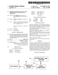
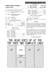
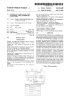
FIG. 1 illustrates a data processing unit 10 connected to
an external bus 12. Although the particular data processing
unit 10 illustrated in FIG. 1 has a RISC (Reduced Instruction
Set Computer) architecture, any architecture or type of data
to read a semaphore, see that the system resource is avail
able, and write back a value to the semaphore to indicate that
the resource is now busy. Thus, locking the bus guarantees
that only one processor at a time will actually use a system
processing unit 10 could be used. Data processing unit 10 is
capable of executing instructions designated by a user in a
software program.
An integer unit 14, a ?oating point unit 16, a graphic unit
18, a load/store execution unit 20, a register ?le 22, and a
superscalar instruction unit 24 are all bi-directionally con
resource. Collisions on the bus are therefore avoided.
However, locking the bus has a very signi?cant drawback.
It may cause communications between other microproces
sors and system resources to slow down considerably. And
as a result, the whole system may operate much more slowly. 15 nected to an internal bus 26. The load/store execution unit 20
is used to control the execution of instructions within the
As an example, a problem may arise when a hierarchical
data processing unit 10. In some embodiments of the present
bus structure utilizing multiple busses is used. If the bus
invention, load/store execution unit 20 may receive an input
master processor and the memory containing the semaphore
from a control pin 27. The register ?le 22 contains infor
are on buses that are very distant from one another, the bus
20 mation registers that can be used to store various types of
master must continuously lock all of the buses between itself
data, such as for example, numerical values and addresses.
and the distant memory during both the read and the
A target instruction cache 28 is connected to the superscalar
subsequent write to the semaphore. This is not a very
instruction unit 24 for transmitting information to the super
effective use of the bus time, especially considering that an
scalar instruction unit 24.
access to a semaphore is usually a very common access in
25
“Memory management unit” may be abbreviated as
a multi-processor system. Thus, locking the bus is not a very
“MMU”. A data cache MMU 30 has a memory management
satisfactory solution.
unit 32, tags 34, and a data cache 36. All of the blocks within
data cache MMU 30 can transfer information to any other
SUMMARY OF THE lNVEN'IION
block within data cache MMU 30. The tags 34 receive
The previously mentioned needs are ful?lled and other 30 information from the load/store execution unit 20. The data
advantages achieved with the present invention. In one form,
cache 36 is bi-directionally connected to the load/store
the present invention comprises an apparatus and method for
execution unit 20. An instruction cache MMU 38 has a
determining access ordering in a data processing system. A
data processing unit is capable of executing an instruction
which has a plurality of steps.
memory management unit 40, tags 42, and an instruction
cache 44. All of the blocks within instruction cache MMU
35
The data processing unit has a ?rst portion for controlling
execution of the instruction. The data processing unit also
has a second portion coupled to the ?rst portion. The second
38 can transfer information to any other block within
instruction cache MMU 38.
The tags 42 and the memory management unit 40 receive
information from the superscalar instruction unit 24. The
instruction cache 44 sends information to the superscalar
instruction unit 24. Memory management unit 32 includes a
control register ?le 46. Control register ?le 46 can be read,
written, and programmed by a user using internal bus 26.
portion has a ?rst logic state and a second logic state. The
second portion causes the ?rst portion to execute the plu
rality of steps in a ?rst order when the second portion is in
the ?rst logic state. And the second portion causes the ?rst
portion to execute the plurality of steps in a second order
The data path for reading and writing the control register ?le
when the second portion is in the second logic state.
46, using the internal bus 26, is through the load/store
The present invention will be understood by one skilled in 45 execution unit 20 and the data cache 36. Also, control
the art from the detailed description below in conjunction
register ?le 46 transmits control information to load/store
with the accompanying drawings.
execution unit 20.
A bus interface 48 is bi-directionally connected to data
BRIEF DESCRIPTION OF THE DRAWINGS
50 cache 36. Bus interface 48 receives information from
memory management unit 32 and memory management unit
FIG. 1 illustrates, in block diagram form, a data process
40. In addition, bus interface 48 send information to tags 34
ing system and a bus in accordance with one embodiment of
and instruction cache 44. Bus interface 48 is also bi
the present invention;
directionally connected to the external bus 12.
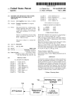
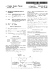
FIG. 2 illustrates, in block diagram form, a control
FIG. 2 illustrates one implementation of the control
register ?le of FIG. 1 in accordance with one embodiment of 55
the present invention; and
FIG. 3 illustrates, in block diagram form, a hierarchical
bus system in accordance with one embodiment of the
present invention.
DESCRIPTION OF THE PREFERRED
EMBODIMENT
Instead of locking the bus, the present invention utilizes
a diiferent approach to guarantee that only one processor at 65
a time will receive a semaphore value which indicates that
a resource is available. The present invention thus ensures
register ?le 46 of FIG. 1. Although the control register ?le
46 is shown to be thirty-two bits wide, other widths could be
used. Also, although this embodiment shows the control
register ?le 46 as part of the memory management unit 32,
the control register ?le 46 could actually be located any
where in data processing unit 10 having access to load/store
execution unit 20. Control register ?le 46 contains several
control registers of which only one, namely the data MMU/
cache control register 50, is illustrated.
The data MMU/cache control register 50 will be referred
to in this speci?cation as control register 50. Control register
50 could have been located anywhere within control register
5,594,880
5
6
?le 46. In fact, control register 50 does not even have to be
a part of control register ?le 46, but instead could be located
Data processing unit 54 must win ownership of all three
busses, 58, 64, and 70, before it can send an address and read
signal to memory 68 across the three busses. Once it
elsewhere in data processing unit 10.
Control register 50 contains an XMEM (exchange register
with memory) control bit 52 (not drawn to scale). In other
embodiments, the XMEM control bit 52 could be located
anywhere convenient in a storage device in data processing
receives an address and read signal, memory 68 internally
accesses the memory location pointed to by the address. The
ownership of all three busses is once again required in order
for memory 68 to send back the data contained in the
accessed memory location. All three busses, 58, 64, and 70,
unit 10. The XMEM control bit 52 would not have to be
located in a control register, although that is usually a
convenient location. Although the XMEM control bit 52 is
located at bit location thirteen of control register 50 in this
embodiment, the XMEM control bit 52 could be located
are involved in both the transfer of address information and
the subsequent transfer of data information.
The advantages of the present invention will be described
using the multi-processor system illustrated in FIG. 3. The
bene?ts of not locking busses is most apparent in a multi
processor system which uses split bus transactions and/or
pipelining. The busses 56, 64, and 70 will thus be considered
to be both split-transaction and pipelined buses in the
present embodiment.
A system which uses split bus transactions is one that
allows different processors to have ownership of the address
bus and data bus at the same time. This type of bus is called
a split-transaction bus. As an example, when a split-trans
action bus is used, microprocessor #1 can use the address
anywhere in control register 50. The other control bits
located in control register 50 are not shown,
The advantages of the present invention are obtained
primarily by the XMEM control bit 52 and the load/store
execution unit 20, along with the associated logic which may
be used in any data processing system. The operation of the
XMEM control bit 52 and its associated logic will be
discussed below.
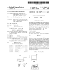
FIG. 3 illustrates a multi-processor system using a hier
archical bus structure. Data processing units 54, 60, and 66
bus at the same time that microprocessor #2 uses the data
can each be any type of data processing unit that has the
bus. In non-split-transaction buses, the same processor is the
XMEM control bit 52 and its associated logic. For the sake
of simplicity, it will be assumed that data processing units 25 bus master of both the address bus and the data bus. Thus
when non-split-transaction buses are used, ownership of the
54, 60, and 66 are all the same as data processing unit 10
address bus and data bus cannot be split. Split-transaction
from FIG. 1.
busses are often used in multi-processor systems in order to
Data processing unit 54 and memory 56 are bi-direction~
increase the bandwidth of the busses.
ally connected to bus 58. Data processing unit 60 and
A pipelined bus is a bus that allows the address phase of
memory 62 are bi-directionally connected to bus 64. Data 30
one transaction to overlap the data phase of another trans
processing unit 66 and memory 68 are bi-directionally
connected to bus 70. Bus 58 is bi-directionally coupled to
bus 64 through bus switch 72. Bus 64 is bi~directionally
coupled to bus 70 through bus switch 74. Bus 64 is bi~
directionally coupled to bus 78 through bus switch 76.
action. Many multi-processor busses combine split-transac
tions and pipelining in order to maximize information trans
fers on both the address bus and the data bus.
35
arrangement of multiple local busses that can communicate
with other busses through bus switches. The processors and
The XMEM control bit 52, illustrated in FIG. 2, is only
used during one particular instruction, an XMEM (exchange
register with memory) instruction. The XMEM instruction
exchanges the contents of memory for the contents of a
other devices on the same local bus can communicate with
register located in register ?le 22in FIG. 1. In other words,
each other using only their local bus. But if a processor
wants to communicate with a device that is on another local
the XMEM instruction swaps the contents of a memory
location with the contents of a register. If the memory
bus, the information must be transferred between the two
local busses by way of one or more bus switches and
location initially contains the value “X” and the register
initially contains the value “Y”, the XMEM instruction will
A hierarchical bus structure, as illustrated in FIG. 3, is an
location in memory 56, only the local bus, bus 58, is required
swap their contents. After execution of the XMEM instruc
tion, the memory location will contain the value “Y” and the
register will contain the value
The XMEM instruction
to carry out the transfer. Data processing unit 54 ?rst
is received and executed in a conventional manner by
arbitrates for bus mastership of bus 58. Note that being the
portions of circuitry illustrated in FIG. 1.
The XMEM instruction is particularly useful in multipro
possibly other intermediate busses.
45
For example, if data processing unit 54 wants to read a
present bus master on a bus is the same as having “owner
ship” of that bus. Once data processing unit 54 has owner
ship of bus 58, data processing unit 54 merely sends an
address to memory 56 across bus 58, along with a signal
indicating that a read is to be performed. After accessing the
appropriate memory location, memory 56 sends back the
data contained in that memory location across bus 58. Only
bus 58 is involved in this transfer of information.
But if data processing unit 54 wants to read a location in
a more distant memory, such as memory 68, then busses 58,
64, and 70 are all required to carry out the transfer. Data
cessor systems that use semaphores. A processor that wants
to use a particular system resource reads the resource’s
semaphore to see if the resource is available. If the resource
is not available, the processor continues to poll the sema
55
phore by periodically reading the semaphore. Once the
semaphore value indicates that the resource is available, the
processor executes an XMEM instruction which ?rst loads
the present value of the semaphore into a register, and then
writes a new value to the semaphore in order to indicate that
the resource is now busy.
The processor then looks at the value of the semaphore
that was loaded into the register in order to determine
whether the resource is busy or available. If the semaphore
indicates that the resource is available, the processor knows
ing unit 54 arbitrates for bus mastership of bus 70 through
bus switch 74. Note that data processing unit 54 is tying up 65 that the resource was available when it started its XMEM
instruction. And because prior art devices required the bus to
the busses it has ownership of while it continues to try to win
be locked during an XMEM instruction, the processor
ownership of the remaining busses.
processing unit 54 ?rst arbitrates for bus mastership of bus
58. Then data processing unit 54 arbitrates for bus master
ship of bus 64 through bus switch 72. Finally, data process
5,594,880
7
8
knows that no other processor has been able to access the
value into the same memory location. The memory also
stores the processor identi?cation value with the buffered
value of the semaphore so that the memory can return the
semaphore between the read and the write portions of the
XMEM instruction. The processor is therefore free to use the
resource with the knowledge that no collision will result.
But if the semaphore loaded into the register during the
XMEM instruction indicates that the resource is busy, the
processor knows that the resource has been taken by another
processor between the last polling read of the semaphore and
the execution of the XMEM instruction. The processor thus
knows not to use the resource, but to instead continue to poll 10
the semaphore until it again indicates that the resource is
available.
In prior art data processing units, an XMEM instruction
for exchanging memory and register contents was accom
panied by a bus lock signal on the bus that indicated when
an XMEM operation was occurring. The memory and the
bus arbitration logic used this bus lock signal to ensure that
the read and subsequent write of the XMEM instruction
were never interrupted by another processor obtaining own
ership of the bus. The bus had to be locked during the
XMEM instruction so that a processor could be guaranteed
that the read and subsequent write of the )MEM instruction
cates that the resource is available. Thus only one processor
at a time will ever receive a semaphore value indicating that
the resource is available.
were performed as an indivisible pair. If any other processor
was allowed to gain ownership of the bus between the read
and the write portions of the XMEM instruction, then the
XMEM would not be useful for semaphore transfers.
proper semaphore value to the proper processor.
At this point in time, any processor that reads the sema
phore will read a value that indicates that the resource is
busy. And any processor that tries to execute an XMEM
instruction will merely rewrite the same value into the
semaphore that indicates that the resource is busy.
The important thing to note is that the semaphore value
received by the second processor is the value previously
written by the ?rst processor: a value that indicates that the
resource is busy. So if the read portion of the XMEM
instruction for the second processor executes before that of
the ?rst processor, the memory will receive the second
processor’s identi?cation value and will return the sema
phore value for the second processor which indicates that the
resource is busy. And when the read portion of the XMEM
instruction for the ?rst processor ?nally executes, the
memory will receive the ?rst processor’ s identi?cation value
and will return the buffered semaphore value which indi
25
Again referring to FIG. 3, assume that data processing
unit 54 wants to access a semaphore located in memory 68.
Processor 54 executes a modi?ed XMEM instruction. The
The present invention, however, does not require busses
to be locked between the XMEM read bus cycle and the
XMEM write bus cycle. Thus, the potential throughput of
the busses in some bus environments is increased signi? 30
?rst bus cycle is a write from data processing unit 54 to
memory 68. Although data processing unit 54 must use all
three busses, 58, 64, and 70, for the write, no bus lock is
cantly. The XMEM instruction in prior art data processing
required. After the single bus cycle write, data processing
units utilized a read (also called a “load”) followed by a
unit 54 relinquishes ownership of the bus and other proces
write (also called a “store”). The present invention allows
the write portion of the XMEM instruction to be performed
sors are free to use the bus. When data processor 54
before the read portion. As a result, the bus does not need to
be locked.
arbitrates for the three busses and again regains ownership,
35
the read portion of the XMEM instruction can be executed
and the data processing unit receives back the proper value
of the semaphore.
Again, the critical coherency is maintained because only
For example, referring to FIG. 3, assume that data pro
cessing unit 54 wants to access a semaphore located in
memory 68. In prior art system, all three busses, 58, 64, and
70, had to be locked during both the read and subsequent
one processor at a time will ever receive back a semaphore
value that indicates that the resource is available. And this
write portion of an XMEM instruction. But the present
coherency is provided without the necessity, required by
invention allows the same XMEM instruction to be per
prior art systems, of locking the bus between the read
portion and the write portion of the XMEM instruction.
Note that the modi?ed XMEM instruction also requires
formed without the necessity of locking all three busses
continuously for both the read and write portions of the
XMEM instruction.
By performing the write portion of the XMEM instruction
?rst, the busses do not have to be locked between the write
and the read portions of the XMEM instruction. The bus
signal that was used to lock the bus in prior art systems can
instead be used merely to indicate that an XMEM instruction
45
50
is currently being performed.
The new way of executing the XMEM instruction that
performs the write before the read will be called the modi
?ed XMEM instruction. The use of the modi?ed XMEM
instruction in semaphore applications will now be described.
55
that the write and read cycles be tagged in some manner to
indicate which processor is executing the modi?ed XMEM
instruction. If this tagging is not done, then the system must
ensure coherency by guaranteeing that the ?rst processor
that writes to the memory during an XMEM transfer is the
only processor that reads and receives the initial semaphore
value indicating that the resource was available. An XMEM
transfer involves the steps occuring during an XMEM
instruction, namely a read bus cycle and a write bus cycle in
some order.
In addition, the present invention allows the user to
determine whether the execution of the XMEM instruction
When the processor executes a modi?ed XMEM instruc
tion, the ?rst bus cycle that occurs is a write to the memory
will be performed as a standard XMEM instruction or as a
location containing the semaphore. The processor always
modi?ed XMEM instruction. The standard XMEM instruc
writes a value that indicates that the resource is busy. During
the same write bus cycle, the processor also sends along a
processor identi?cation value so the memory knows which
tion, which is still required for many existing bus environ
ments, executes a read cycle followed by a write cycle. The
modi?ed XMEM instruction, which is needed to improve
bandwidth in split-transaction bus systems, executes a buff
processor has begun the XMEM instruction. A bus signal
ered write cycle followed by a read cycle.
can be used to indicate that an XMEM instruction is cur
rently being performed. When the memory receives the
write from the processor, the memory ?rst loads the existing
value of the semaphore into a buffer, and then writes the new
65
In the present embodiment, the user uses a control register
bit to determine whether the XMEM instruction will be
performed as a standard )GVIEM instruction or as a modi?ed
5,594,880
9
10
XMEM instruction. The control bit used is the XMEM
control bit 52 illustrated in FIG. 2. In the present embodi
ment, if the XMEM control bit 52 is a binary zero value,
which corresponds to a digital logic state “zero”, a standard
XMEM instruction is performed. If the XMEM control bit
52 is a binary one value, which corresponds to a digital logic
state “one”, a modi?ed XMEM instruction is performed.
required to carry out the XMEM instruction. The same steps
or tasks are always performed when the XMEM instruction
is executed, regardless of the logic state of the XMEM
control bit 52. Only the ordering of the steps or tasks is
changed. Thus the result or outcome of the instruction is
identical to the user. The outcome or result of both the
standard and the modi?ed XMEM instruction is the
exchanging or swapping of the values in a register and a
Alternatively, in other embodiments of the present inven
tion, control pin 27 can be used instead of XMEM control
memory location. But the fact that the user can choose the
bit 52 as an alternate way to allow the user to select the type 10 ordering of the steps used to execute this instruction can
result in a signi?cant improvement in bus bandwidth in
certain bus environments.
Although the present invention has been described in the
context of a speci?c instruction, the XMEM instruction, the
present invention could be used with any instruction that has
of XMEM instruction to be performed. By placing on
control pin 27 either a voltage corresponding to a digital
logic state “one” or a voltage corresponding to a digital logic
state “zero”, the user can select the type of XMEM instruc
tion to be performed. As is shown in FIG. 1, the control pin
27 can be connected directly to the load/store execution unit
20. The pin may or may not be coupled to the external bus
12. Alternatively, the pin can be connected to the external
bus 12 and the bus interface 48. In this alternate case, the
more than one step or task. The present invention allows the
user to change the ordering of the steps or tasks of an
instruction. Although the XMEM instruction as presently
discussed only has two possible orderings, other embodi
load/store execution unit 20 can receive the control infor
mation from the pin by way of instruction cache 44, super
scalar instruction unit 24, and internal bus 26.
Alternatively, in yet other embodiments of the present
ments of the present invention may use multiple control bits
20
in order to choose between multiple possible orderings of
the steps or tasks of the chosen instruction.
While the present invention has been illustrated and
invention, a bit ?eld of one or more bits within the binary
described with reference to speci?c embodiments, further
encoding of the instruction itself can be used, instead of a
modi?cations and improvements will occur to those skilled
control register bit, as an alternate way to allow the user to 25 in the art.
select the type of XMEM instruction to be performed. The
instruction in one embodiment of the present embodiment
It is to be understood, therefore, that this invention is not
limited to the particular forms illustrated and that it is
intended in the appended claims to cover all modi?cations
that do not depart from the spirit and scope of this invention.
What is claimed is:
1. A data processing unit for executing a software instruc
tion, the software instruction having a multi-bit binary
consists of thirty-two bits arranged in a plurality of bit ?elds.
In other embodiments, more or less than thirty-two total bits
may be used. By placing the proper binary value in the
proper bit ?eld of the XMEM instruction, the user can select
the type of XMEM instruction to be performed. For
example, a bit ?eld of one bit could be used with a binary
zero value to represent a standard XMEM instruction, and a
representation, the software instruction including a plurality
binary one value to represent a modi?ed XMEM instruction. 35 of tasks, the data processing unit comprising:
Referring to FIG. 1, if a bit ?eld within the XMEM
instruction is used to select the ordering of the steps or tasks
of the XMEM instruction, the XMEM instruction is still
received by the data processing unit 10 in the same manner
as other instructions. Like other instructions, the XMEM
instruction is received by bus interface 48 from external bus
12. The various bit ?elds of the XMEM instruction are used
in the same manner as the bit ?elds of other instructions,
with the exception of the bit ?eld used to select the ordering
of the steps or tasks of the XMEM instruction. This task 45
ordering bit ?eld is transferred to the load/store execution
unit 20 which is used to control the execution of instructions.
In the present embodiment, the task ordering bit ?eld is
transferred to the load/store execution unit 20 by way of
instruction cache 44, superscalar instruction unit 24, and
internal bus 26.
In summation, the modi?ed XMEM instruction allows the
bandwidth of split-transaction busses to be potentially
50
increased by doing away with the requirement of locking the
a bus interface circuit for receiving the multi-bit binary
representation of the software instruction from a bus;
an instruction storage circuit having a plurality of storage
elements, a ?rst one of the plurality of storage elements
storing the multi-bit binary representation of the soft
ware instruction, said instruction storage circuit being
coupled to said bus interface circuit;
control means for providing a control value; and
execution means for controlling execution of the software
instruction, during execution of the software instruction
said execution means receives the multi-bit binary
representation from said instruction storage circuit and
receives the control value from said control means and,
in response thereto, executes said plurality of tasks of
the software instruction in a ?rst order if the control
value has a ?rst value, and executes said plurality of
tasks of the software instruction in a second order if the
control value has a second value, said execution means
being coupled to said instruction storage circuit and to
busses during an XMEM transfer. The XMEM control bit 52 55
said control means.
allows users to choose the XMEM instruction that is optimal
2. A data processing unit according to claim 1, wherein
for their system. Users that have systems with standard bus
said control means comprises:
environments can choose the standard XMEM instruction.
at least a portion of a user programmable control register.
And users with split-transaction busses and more complex
3. A data processing unit according to claim 1, wherein
bus environments can choose the modi?ed XMEM instruc
said control means is a portion of the multi-bit binary
tion. This software control allows the same data processing
representation of the software instruction.
unit 10 to supply the needs of users utilizing very different
4. A data processing unit according to claim 1, wherein
bus environments. This software control also allows users to
said control means comprises:
optimize the data processing unit 10 for their particular
system.
It is important to note that the )QVIEM control bit 52
merely changes the ordering of the steps or tasks that are
65
an integrated circuit pin.
5. A method according to claim 1, wherein the software
instruction has a nmemonic form of “XMEM”.
5,594,880
11
12
6. A data processing unit according to claim 1, wherein the
16. A method for determining an ordering of a plurality of
plurality of tasks includes a read task and a write task.
tasks required to execute an instruction in a data processing
7. A data processing unit according to claim 6, wherein the
unit, the method comprising the steps of:
representing the instruction by way of a plurality of bit
data processing unit further comprises:
a data register coupled to the bus interface circuit; and
wherein the read task includes a read bus cycle which
transfers a ?rst data value from the bus to said data
register, and wherein the write task includes a write bus
cycle which transfers a second data value from said
data register to the bus.
?eld values, a ?rst one of the plurality of bit ?eld values
having a predetermined ?xed value, a second one of the
plurality of bit ?eld values having a user determinable
control value;
10
8. A data processing unit according to claim 7, wherein the
?rst and second data values are semaphore values.
-
selecting the user determinable control value for the
second one of the plurality of bit ?eld values;
providing the plurality of bits ?eld values to the data
processing unit;
9. A data processing unit according to claim 7, wherein the
binary representation, the ?rst software instruction having at
if the control value has a ?rst value, executing said
plurality of tasks in a ?rst order; and
if the control value has a second value, executing said
plurality of tasks in a second order.
17. The method according to claim 16 wherein the plu
rality of tasks includes a read bus cycle and a write bus
least one task, the second software instruction having a 20
cycle.
plurality of tasks, the data processing unit comprising:
18. A method according to claim 16, wherein said step of
executing said plurality of tasks in a ?rst order comprises the
step of:
read bus cycle and the write bus cycle each access a same
memory location.
10. A data processing unit for executing a ?rst software
instruction having a ?rst multi-bit binary representation and
a second software instruction having a second multi-bit
a bus interface circuit for receiving, from a bus, the ?rst
multi-bit binary representation of the ?rst software
instruction and the second multi-bit binary representa
tion of the second software instruction;
25
an instruction storage circuit having a ?rst element for
storing the ?rst multi-bit binary representation of the
?rst software instruction and for simultaneously storing
the second multi-bit binary representation of the second
software instruction, said instruction storage circuit
being coupled to said bus interface circuit;
a control register, said control register having a register
portion for storing a control value;
a data register, coupled to said bus interface circuit; and
30
exchanging a ?rst data value stored in a register with a
second data value stored in a memory location; and
wherein said step of executing said plurality of tasks in a
second order comprises the step of:
exchanging the ?rst data value stored in the register with
the second data value stored in the memory location.
19. A method according to claim 18, wherein each of said
steps of exchanging comprises the steps of:
thereto causes the control value to be provided to and
transferring the ?rst data value by way of a split transac
tion bus; and
transferring the second data value by way of the split
transaction bus.
20. A method according to claim 19, wherein the split
transaction bus is pipelineable.
21. A method according to claim 16, wherein said step of
executing said plurality of tasks in a ?rst order comprises the
step of:
stored in the register portion, during execution of the
performing a read access to a selected address before
35
execution means for controlling execution of the ?rst
software instruction and the second software instruc
tion, during execution of the at least one task of the ?rst
software instruction said execution means decodes the
?rst multi-bit binary representation and in response
second software instruction said execution means
performing a write access to the selected address; and
decodes the second multi-bit binary representation and
receives the control value from the register portion and,
in response thereto, executes said plurality of tasks in
wherein said step of executing said plurality of tasks in a
second order comprises the step of:
performing the write access to the selected address before
45
a ?rst order if the control value has a ?rst value and
executes said plurality of tasks in a second order if the
control value has a second value, said execution means
being coupled to said instruction storage circuit and to
said control register.
11. A method according to claim 10, wherein the second
performing the read access to the selected address.
22. A method according to claim 21, wherein each of said
steps of performing comprises the step of:
50
software instruction has a mnemonic form of “XMEM”.
12. A data processing unit according to claim 10 wherein
transferring data by Way of a split transaction bus.
23. A method according to claim 21, further comprising
the step of:
storing a semaphore at the selected address.
24. A method according to claim 21, wherein the instruc
the ?rst order of the plurality of tasks includes a read task 55
tion has a mnemonic form of “XME ”.
followed by a write task, and wherein the second order of the
25. A method for operating a data processing system, the
plurality of tasks includes the write task followed by the read
data
processing system having a ?rst processor, a second
task.
processor, and a memory coupled to both the ?rst and second
13. A data processing unit according to claim 10, wherein
processors by way of a bus, the memory having a memory
the ?rst value of the control value is a binary zero and the
storage circuit, the method comprising the steps of:
second value of the control value is a binary one.
14. A data processing unit according to claim 10, wherein
the software instruction exchanges a ?rst data value stored
in said data register with a second data value stored in a
memory location.
65
15. A data processing unit according to claim 14, wherein
the ?rst and second data values are semaphore values.
determining a control value, the control value correspond
ing to an instruction;
initiating execution of the instruction in the ?rst proces
sor;
'
using the control value to select, as a selected ordering,
one of a ?rst ordering of a plurality of tasks for the
5,594,880
14
13
instruction and a second ordering of the plurality of
tasks for the instruction;
if the ?rst ordering is selected, performing the following
steps:
transferring the old data value from the temporary
storage circuit to the ?rst processor by way of the bus
during the read bus cycle; and
initiating a write bus cycle on the bus from the ?rst 5
processor to the memory;
if the second ordering is selected, initiating the read bus
cycle before initiating the write bus cycle.
transferring a new data value from the ?rst processor to
26. A method according to claim 25, wherein the bus is a
the memory by way of the bus during the write bus
cycle;
split transaction bus.
transferring a ?rst processor identi?cation value from 10
27. A method according to claim 25, wherein the instruc~
the ?rst processor to the memory by way of the bus
tion has a mnemonic form of “XME ”.
during the write bus cycle;
28. A method according to claim 25 wherein the old data
transferring an old data value from the memory storage
value
is an old semaphore value, and the new data value is
circuit to a temporary storage circuit;
storing the ?rst processor identi?cation value so that it
a new semaphore value.
is associated with the old data value;
29. A method according to claim 25, wherein if the ?rst
overwriting the old data value with the new data value
so that the new data value is stored in the memory
storage circuit;
ordering is selected, performing the following step:
after initiating the write bus cycle, but before initiating the
after initiating the write bus cycle, initiating a read bus
read bus cycle, transferring the new data value from the
cycle on the bus from the memory to the ?rst
processor;
transferring the ?rst processor identi?cation value from
the ?rst processor to the memory by way of the bus
request by the second processor.
during the read bus cycle; and
memory to the second processor in response to a


