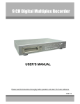
1
TQMa335x
Preliminary User's Manual
TQMa335x UM 002
26.11.2013
Preliminary User's Manual l TQMa335x UM 002 l © 2013 TQ-Group
Page i
TABLE OF CONTENTS
1.
1.1
1.2
1.3
1.4
1.5
1.6
1.7
1.8
1.9
2.
2.1
3.
3.1
3.1.1
3.1.2
3.2
3.2.1
3.2.2
3.2.2.1
3.2.2.2
3.2.2.3
3.2.2.4
3.2.2.5
3.2.3
3.2.3.1
3.2.3.2
3.2.3.3
3.2.3.4
3.2.4
3.2.5
3.2.6
3.2.7
3.2.8
3.2.9
3.2.10
3.2.11
3.2.12
3.2.13
3.2.14
3.2.15
3.2.16
3.2.17
3.2.18
3.2.18.1
3.2.18.2
3.2.18.3
3.2.19
3.2.20
3.2.21
3.2.21.1
3.2.21.2
3.2.22
3.2.22.1
3.2.22.2
3.2.22.3
3.2.22.4
3.2.22.5
3.2.22.6
ABOUT THIS MANUAL ........................................................................................................................................................................1
Copyright and licence expenses.....................................................................................................................................................1
Registered trademarks.......................................................................................................................................................................1
Disclaimer ..............................................................................................................................................................................................1
Imprint ....................................................................................................................................................................................................1
Tips on safety ........................................................................................................................................................................................2
Symbols and typographic conventions........................................................................................................................................2
Handling and ESD tips........................................................................................................................................................................2
Naming of signals................................................................................................................................................................................3
Further applicable documents / presumed knowledge..........................................................................................................3
BRIEF DESCRIPTION.............................................................................................................................................................................4
Key functions and characteristics ...................................................................................................................................................4
ELECTRONICS SPECIFICATION .........................................................................................................................................................5
System overview..................................................................................................................................................................................5
System architecture / block diagram.............................................................................................................................................5
Functionality .........................................................................................................................................................................................5
System components...........................................................................................................................................................................6
AM335xprocessor................................................................................................................................................................................6
AM335x processor versions..............................................................................................................................................................6
Boot configuration ..............................................................................................................................................................................7
Boot interfaces......................................................................................................................................................................................7
Boot device SD card............................................................................................................................................................................7
Boot device eMMC ..............................................................................................................................................................................8
Boot device SPI NOR flash.................................................................................................................................................................8
Memory...................................................................................................................................................................................................9
DDR3L SDRAM......................................................................................................................................................................................9
eMMC NAND flash...............................................................................................................................................................................9
Serial NOR ........................................................................................................................................................................................... 10
EEPROM ............................................................................................................................................................................................... 10
Temperature sensor......................................................................................................................................................................... 11
RTC ........................................................................................................................................................................................................ 11
Ethernet ............................................................................................................................................................................................... 12
SD card................................................................................................................................................................................................. 13
GPIO ...................................................................................................................................................................................................... 13
JTAG...................................................................................................................................................................................................... 13
Touch and Analog Inputs............................................................................................................................................................... 14
External Memory Bus....................................................................................................................................................................... 14
LCD-Controller................................................................................................................................................................................... 15
Serial interfaces ................................................................................................................................................................................. 16
CAN ....................................................................................................................................................................................................... 16
I2C.......................................................................................................................................................................................................... 16
I2S .......................................................................................................................................................................................................... 17
SPI.......................................................................................................................................................................................................... 17
UART ..................................................................................................................................................................................................... 18
UART0................................................................................................................................................................................................... 18
UART3................................................................................................................................................................................................... 18
UART4................................................................................................................................................................................................... 19
USB........................................................................................................................................................................................................ 19
Reset ..................................................................................................................................................................................................... 20
Power supply ..................................................................................................................................................................................... 21
Main power supply........................................................................................................................................................................... 21
Overview module supply ............................................................................................................................................................... 21
Power Modes ..................................................................................................................................................................................... 21
RTC Backup......................................................................................................................................................................................... 21
AM335x RTC-Only............................................................................................................................................................................. 22
AM335x DEEP-SLEEP0-2, Standby ............................................................................................................................................... 22
AM335x Active Mode ...................................................................................................................................................................... 22
Module / carrier board Power-Up sequence............................................................................................................................ 23
Battery input VBACKUP................................................................................................................................................................... 23
Preliminary User's Manual l TQMa335x UM 002 l © 2013 TQ-Group
Page ii
TABLE OF CONTENTS (continued)
3.3
3.3.1
3.3.2
3.3.3
4.
4.1
4.2
4.3
4.4
4.5
4.6
4.7
4.8
5.
6.
6.1
6.2
6.3
6.4
6.5
6.6
6.6.1
6.6.2
6.7
6.8
7.
7.1
7.2
Module interface............................................................................................................................................................................... 23
Pin assignment.................................................................................................................................................................................. 23
Pinout connector X1........................................................................................................................................................................ 24
Pinout connector X2........................................................................................................................................................................ 25
MECHANICS........................................................................................................................................................................................ 26
Module connectors.......................................................................................................................................................................... 26
Dimensions......................................................................................................................................................................................... 27
Component placement .................................................................................................................................................................. 28
Adaptation to the environment................................................................................................................................................... 29
Protection against external effects ............................................................................................................................................. 29
Thermal management .................................................................................................................................................................... 29
Structural requirements ................................................................................................................................................................. 29
Notes of treatment........................................................................................................................................................................... 29
SOFTWARE .......................................................................................................................................................................................... 29
SAFETY REQUIREMENTS AND PROTECTIVE REGULATIONS ................................................................................................. 30
EMC ....................................................................................................................................................................................................... 30
ESD ........................................................................................................................................................................................................ 30
Operational safety and personal security ................................................................................................................................. 30
Climatic and operational conditions .......................................................................................................................................... 30
Reliability and service life............................................................................................................................................................... 31
Environment protection................................................................................................................................................................. 31
RoHS compliance.............................................................................................................................................................................. 31
WEEE regulation................................................................................................................................................................................ 31
Batteries............................................................................................................................................................................................... 31
Other entries ...................................................................................................................................................................................... 31
APPENDIX............................................................................................................................................................................................ 32
Acronyms and definitions.............................................................................................................................................................. 32
References........................................................................................................................................................................................... 34
Preliminary User's Manual l TQMa335x UM 002 l © 2013 TQ-Group
Page iii
TABLE DIRECTORY
Table 1:
Table 2:
Table 3:
Table 4:
Table 5:
Table 6:
Table 7:
Table 8:
Table 9:
Table 10:
Table 11:
Table 12:
Table 13:
Table 14:
Table 15:
Table 16:
Table 17:
Table 18:
Table 19:
Table 20:
Table 21:
Table 22:
Table 23:
Table 24:
Table 25:
Table 26:
Table 27:
Table 28:
Table 29:
Table 30:
Table 31:
Table 32:
Table 33:
Table 34:
Table 35:
Table 36:
Table 37:
Table 38:
Table 39:
Table 40:
Table 41:
Terms and Conventions.....................................................................................................................................................................2
Processor versions...............................................................................................................................................................................6
Boot device selection .........................................................................................................................................................................7
Oscillator frequency............................................................................................................................................................................7
Pins used for SD card boot................................................................................................................................................................7
Pins used for eMMC boot..................................................................................................................................................................8
Pins used for SPI NOR flash boot.....................................................................................................................................................8
DDR3 SDRAM ........................................................................................................................................................................................9
DDR3-SDRAM address range ...........................................................................................................................................................9
EEPROM ............................................................................................................................................................................................... 10
Temperature sensor......................................................................................................................................................................... 11
Current consumption RTC ............................................................................................................................................................. 11
RGMII1 .................................................................................................................................................................................................. 12
RGMII2 .................................................................................................................................................................................................. 12
SD card signals................................................................................................................................................................................... 13
GPIO signals........................................................................................................................................................................................ 13
JTAG signals........................................................................................................................................................................................ 13
Touch signals ..................................................................................................................................................................................... 14
LCD signals ......................................................................................................................................................................................... 15
CAN1 / CAN2 signals........................................................................................................................................................................ 16
I2C2 signals......................................................................................................................................................................................... 16
I2C2 address distribution ............................................................................................................................................................... 16
I2S signals............................................................................................................................................................................................ 17
SPI signals............................................................................................................................................................................................ 17
UART0 signals .................................................................................................................................................................................... 18
UART3 signals .................................................................................................................................................................................... 18
UART4 signals .................................................................................................................................................................................... 19
USB_H1 signals.................................................................................................................................................................................. 19
Reset signals....................................................................................................................................................................................... 20
Parameter module supply ............................................................................................................................................................. 21
External RTC ....................................................................................................................................................................................... 21
PMIC RTC ............................................................................................................................................................................................. 21
AM335x RTC-Only............................................................................................................................................................................. 22
AM335x DEEP-SLEEP0-2, Standby ............................................................................................................................................... 22
AM335x Active Mode ...................................................................................................................................................................... 22
Pinout connector X1........................................................................................................................................................................ 24
Pinout connector X2........................................................................................................................................................................ 25
Plug connector (receptacle) used on the TQMa335x ............................................................................................................ 26
Suitable carrier board mating plug connectors...................................................................................................................... 26
Acronyms ............................................................................................................................................................................................ 32
Further applicable documents..................................................................................................................................................... 34
Preliminary User's Manual l TQMa335x UM 002 l © 2013 TQ-Group
Page iv
ILLUSTRATION DIRECTORY
Illustration 1:
Illustration 2:
Illustration 3:
Illustration 4:
Illustration 5:
Illustration 6:
Illustration 7:
Illustration 8:
Illustration 9:
Illustration 10:
Illustration 11:
Illustration 12:
Illustration 13:
Illustration 14:
Illustration 15:
Illustration 16:
Illustration 17:
Block diagram TQMa335x (simplified)...................................................................................................................................4
Block diagram TQMa335x..........................................................................................................................................................5
Block diagram AM335x...............................................................................................................................................................6
Block diagram DDR3L SDRAM connection...........................................................................................................................9
Block diagram eMMC flash connection.................................................................................................................................9
Block diagram SPI NOR flash connection........................................................................................................................... 10
Block diagram EEPROM connection.................................................................................................................................... 10
Block diagram temperature sensor connection .............................................................................................................. 11
Block diagram UART0 interface ............................................................................................................................................ 18
Block diagram UART3 interface ............................................................................................................................................ 18
Block diagram UART4 interface ............................................................................................................................................ 19
Block diagram Reset ................................................................................................................................................................. 20
Block diagram power supply ................................................................................................................................................. 21
Block diagram power supply carrier board....................................................................................................................... 23
Overall dimensions (top view)............................................................................................................................................... 27
Component placement top ................................................................................................................................................... 28
Component placement bottom ........................................................................................................................................... 28
Preliminary User's Manual l TQMa335x UM 002 l © 2013 TQ-Group
REVISION HISTORY
Rev.
Date
Name
001
09.09.2013
Petz
002
26.11.2013
Petz
Pos.
Modification
Preliminary document created
All
Complete rework
Page v
Preliminary User's Manual l TQMa335x UM 002 l © 2013 TQ-Group
1.
ABOUT THIS MANUAL
1.1
Copyright and licence expenses
Page 1
Copyright protected © 2013 by TQ-Systems GmbH.
This Preliminary User's Manual may not be copied, reproduced, translated, changed or distributed, completely or partially in
electronic, machine readable, or in any other form without the written consent of TQ-Systems GmbH.
The drivers and utilities for the used components as well as the BIOS are subject to the copyrights of the respective
manufacturers. The licence conditions of the respective manufacturer are to be adhered to.
Bootloader-licence expenses are paid by TQ-Systems GmbH and are included in the price.
Licence expenses for the operating system and applications are not taken into consideration and must be separately calculated /
declared.
1.2
Registered trademarks
TQ-Systems GmbH aims to adhere to the copyrights of all the graphics and texts used in all publications, and strives to use
original or license-free graphics and texts.
All the brand names and trademarks mentioned in the publication, including those protected by a third party, unless specified
otherwise in writing, are subjected to the specifications of the current copyright laws and the proprietary laws of the present
registered proprietor without any limitation. One should conclude that brand and trademarks are rightly protected by of a third
party.
1.3
Disclaimer
TQ-Systems GmbH does not guarantee that the information in this Preliminary User's Manual is up-to-date, correct, complete or
of good quality. Nor does TQ-Systems GmbH assume guarantee for further usage of the information. Liability claims against TQSystems GmbH, referring to material or non-material related damages caused, due to usage or non-usage of the information
given in the Preliminary User's Manual, or due to usage of erroneous or incomplete information, are exempted, as long as there is
no proven intentional or negligent fault of TQ-Systems GmbH.
TQ-Systems GmbH explicitly reserves the rights to change or add to the contents of this Preliminary User's Manual or parts of it
without special notification.
1.4
Imprint
TQ-Systems GmbH
Gut Delling, Mühlstraße 2
82229 Seefeld
Tel:
+49 (0) 8153 9308–0
Fax:
+49 (0) 8153 9308–134
Email: info@tqs.de
http://www.tq-group.com/
Web:
Preliminary User's Manual l TQMa335x UM 002 l © 2013 TQ-Group
1.5
Page 2
Tips on safety
Improper or incorrect handling of the product can substantially reduce its life span.
1.6
Symbols and typographic conventions
Table 1:
Symbol
Terms and Conventions
Meaning
This symbol represents the handling of electrostatic-sensitive modules and / or components. These
components are often damaged / destroyed by the transmission of a voltage higher than about 50 V.
A human body usually only experiences electrostatic discharges above approximately 3,000 V.
This symbol indicates the possible use of voltages higher than 24 V.
Please note the relevant statutory regulations in this regard.
Non-compliance with these regulations can lead to serious damage to your health and also cause
damage / destruction of the component.
This symbol indicates a possible source of danger. Acting against the procedure described can lead to
possible damage to your health and / or cause damage / destruction of the material used.
This symbol represents important details or aspects for working with TQ-products.
Command
1.7
A font with fixed-width is used to denote commands, file names, or menu items.
Handling and ESD tips
General handling of your TQ-products
The TQ-product may only be used and serviced by certified personnel who have taken note of the
information, the safety regulations in this document and all related rules and regulations.
A general rule is: do not touch the TQ-product during operation. This is especially important when
switching on, changing jumper settings or connecting other devices without ensuring beforehand
that the power supply of the system has been switched off.
Violation of this guideline may result in damage / destruction of the TQMa335x and be dangerous
to your health.
Improper handling of your TQ-product would render the guarantee invalid.
Proper ESD handling
The electronic components of your TQ-product are sensitive to electrostatic discharge (ESD).
Always wear antistatic clothing, use ESD-safe tools, packing materials etc., and operate your TQproduct in an ESD-safe environment. Especially when you switch modules on, change jumper settings,
or connect other devices.
Preliminary User's Manual l TQMa335x UM 002 l © 2013 TQ-Group
1.8
Page 3
Naming of signals
A hash mark (#) at the end of the signal name indicates a low-active signal.
Example: RESET#
If a signal can switch between two functions and if this is noted in the name of the signal, the low-active function is marked with
a hash mark and shown at the end.
Example: C / D#
If a signal has multiple functions, the individual functions are separated by slashes when they are important for the wiring.
The identification of the individual functions follows the above conventions.
Example: WE2# / OE#
1.9
Further applicable documents / presumed knowledge
•
•
•
•
•
Specifications and manual of the used modules:
These documents describe the service, functionality and special characteristics of the used module (incl. BIOS).
Specifications of the used components:
The manufacturer's specifications of the used components, for example CompactFlash cards, are to be taken note of.
They contain, if applicable, additional information that must be taken note of for safe and reliable operation.
These documents are stored at TQ-Systems GmbH.
Chip errata:
It is the user's responsibility to make sure all errata published by the manufacturer of each component are taken note of.
The manufacturer’s advice should be followed.
Software behaviour:
No warranty can be given, nor responsibility taken for any unexpected software behaviour due to deficient components.
General expertise:
Expertise in electrical engineering / computer engineering is required for the installation and the use of the device.
The following documents are required to fully comprehend the following contents:
•
•
•
•
•
Circuit diagram MBa335x
CPU Reference Manual SPRS717F
Preliminary User's Manual STK-MBa335x
Documentation of boot loader U-Boot
Documentation of PTXdist
(http://www.denx.de/wiki/U-Boot/Documentation)
(http://www.ptxdist.de)
Preliminary User's Manual l TQMa335x UM 002 l © 2013 TQ-Group
2.
Page 4
BRIEF DESCRIPTION
This Preliminary User's Manual describes the hardware of the TQMa335x, and refers to some software settings.
It does not replace the Reference Manual of the CPU. The TQMa335x is a universal Minimodule based on the Texas Instruments
AM335x. The Cortex A8 core of this CPU works with up to 800 MHz. The TQMa335x extends the TQC product range and offers an
outstanding computing performance.
Illustration 1:
Block diagram TQMa335x (simplified)
The TQMa335x provides the following key functions and characteristics:
2.1
Key functions and characteristics
•
•
•
•
•
•
•
•
•
•
•
•
•
•
•
•
DDR3L SDRAM
SPI NOR flash
eMMC flash
Up to 2 × Ethernet 10/100/1000 Mbit (L2 Switch)
Up to 2 × CAN 2.0B
Up to 6 × UART
2 × USB 2.0 High-Speed interface with PHY
Up to 2 × SDIO/MMC
Up to 3 × I2C
Up to 2 × McASP (4-ch)
Up to 2 × SPI
GPIOs
Up to 8 × 12 bit ADC channels
Up to 3 × PWM
24 bit graphics for displays incl. backlight control (PWM), BKL on/off
Touch (4-wire resistive)
All useful signals of the microprocessor are routed to the connectors.
There are no restrictions for customers using the TQMa335x with respect to an integrated customised design.
Please take note of that not all listed interfaces can be used simultaneously.
Preliminary User's Manual l TQMa335x UM 002 l © 2013 TQ-Group
3.
ELECTRONICS SPECIFICATION
3.1
System overview
3.1.1
System architecture / block diagram
Illustration 2:
3.1.2
Block diagram TQMa335x
Functionality
The following key functions are implemented on the TQMa335x:
•
•
•
•
•
•
•
•
AM335x CPU (-2, -4, -8, -9) other on request
DDR3L SDRAM, up to 512 Mbyte
eMMC NAND flash, up to 16 Gbyte
SPI NOR flash, up to 128 Mbyte
EEPROM, 0 or 64 Kbyte (assembly option)
Temperature sensor
PMIC
RTC
Page 5
Preliminary User's Manual l TQMa335x UM 002 l © 2013 TQ-Group
3.2
System components
3.2.1
AM335xprocessor
Page 6
The following illustration shows the block diagram of the AM335x processor family:
Illustration 3:
3.2.2
Block diagram AM335x
(Source: Texas Instruments)
AM335x processor versions
Depending on the version of the TQMa335x one of the following versions of the CPU is assembled:
Table 2:
Processor versions
Manufacturer
Part number
Temperature range
Package
Texas Instruments
AM3352BZCZD80
–40 °C to +90 °C
PBGA324 (ZCZ)
Texas Instruments
AM3354BZCZD80
–40 °C to +90 °C
PBGA324 (ZCZ)
Texas Instruments
AM3359BZCZA80
–40 °C to +105 °C
PBGA324 (ZCZ)
Attention: Malfunction
Please take note of the current errata of the AM335x (7).
Preliminary User's Manual l TQMa335x UM 002 l © 2013 TQ-Group
3.2.2.1
Page 7
Boot configuration
The boot configuration of the TQMa335x is defined through 16 GPIO pins. None of these 16 boot configuration pins are
connected on the TQMa335x, which means, the TQMa335x is delivered with no preset boot configuration.
The boot-configuration is read from register sysboot[15:0]. Register sysboot is read from pins LCD_DATA[15:0].
It is recommended to connect 10 kΩ pull-up or pull-down resistors.
The settings for other boot devices are to be taken from the data sheet of the AM335x CPU (1).
The following tables shows the configuration which can be used with the BSP and the MBA335x of TQ-Systems GmbH.
Table 3:
Boot device selection
SYSBOOT[4:0]
Boot Sequence
1st
2nd
3rd
4th
10111b
MMC0 / SD
MCSPI0 / NOR
UART0 / n.a.
USB0 / n.a.
11100b
MMC1/ eMMC
MMC0 / SD
UART0 / n.a.
USB0 / n.a.
11000b
MCSPI0 / NOR
MMC0 / SD
USB0 / n.a.
UART0 / n.a.
The bits SYSBOOT[15:14] set the frequency of the oscillator.
The values in the following table printed in bold are used on account of the 24 MHz oscillator assembled on the TQMa335x.
Table 4:
Oscillator frequency
SYSBOOT[15:14]
Oscillator frequency / MHz
Remark
00b
19.2
–
01b
24
Default
10b
25
–
11b
26
–
Bit SYSBOOT[5] indicates whether CLKOUT1is configured as an output after a reset. This can be set accordingly.
The remaining values of SYSBOOT[13:6] have to be set to “0”.
These settings exclusively support the above described boot sequences.
3.2.2.2
Boot interfaces
The configuration of the following boot devices is described in the next sections:
• MMC0 (external SD card)
• MCSPI0 (internal NOR flash)
• MMC1 (internal eMMC)
3.2.2.3
Boot device SD card
The SD card boots from MMC0. The boot ROM does not support card_detect.
Booting from SD card supports the binary raw mode and FAT.
The following pins must be used for the boot process.
Table 5:
Pins used for SD card boot
Signal name
Pin used in device
CLK
CMD
DAT0
DAT1
DAT2
DAT3
MMC0_CLK
MMC0_CMD
MMC0_DAT0
MMC0_DAT1
MMC0_DAT2
MMC0_DAT3
Preliminary User's Manual l TQMa335x UM 002 l © 2013 TQ-Group
3.2.2.4
Page 8
Boot device eMMC
The eMMC boots from MMC1. MMC1supports eMMCs with a memory size of 4 Gbyte or greater.
Booting from eMMC supports the binary raw mode and FAT.
The maximum bus width to boot from is 4 bits, initially it is 1 bit.
The following pins have to be used for the boot process.
Table 6:
Pins used for eMMC boot
Signal name
Pin used in device
Remark
CLK
GPMC_CSN1
–
CMD
GPMC_CSN2
–
DAT0
GPMC_AD0
4-bit boot
DAT1
GPMC_AD1
4-bit boot
DAT2
GPMC_AD2
4-bit boot
DAT3
GPMC_AD3
4-bit boot
DAT4
GPMC_AD4
Not for booting
DAT5
GPMC_AD5
Not for booting
DAT6
GPMC_AD6
Not for booting
DAT7
GPMC_AD7
Not for booting
3.2.2.5
Boot device SPI NOR flash
The SPI flash has to be connected to SPI0 / CS0. 12 MHz (50% duty cycle) are supported.
Only SPI mode 3 is supported (SPICLK active low, sampling with rising edge).
The SPI-FLASH has to be 24 bits addressable and has to support the command “read 03h“.
The following pins have to be used for the boot process.
Table 7:
Pins used for SPI NOR flash boot
Signal name
Pin used in device
CS
SPI0_CS0
MISO
SPI0_D0
MOSI
SPI0_D1
CLK
SPI0_SCLK
HOLD#
WARMRST#
For other boot-configurations please refer to the data sheet of the AM335x CPU (1).
Attention: Destruction or malfunction
Many of the CPU pins permit the usage of several different configurations.
Please pay attention to the notes in the data sheet of the AM335x CPU (1) concerning the wiring of
these pins before integration / start-up of your carrier board / Starterkit.
Preliminary User's Manual l TQMa335x UM 002 l © 2013 TQ-Group
3.2.3
3.2.3.1
Memory
DDR3L SDRAM
The TQMa335x is equipped with one DDR3L SDRAM chip with a data bus width of 16 bits.
The following block diagram shows how the DDR3L SDRAM is connected to the processor.
Illustration 4:
Block diagram DDR3L SDRAM connection
The TQMa335x can be equipped with 256 Mibyte or 512 Mibyte of DDR3L SDRAM:
Table 8:
DDR3 SDRAM
Placement option
Size
Remark
1 × DDR3L 128M16
256 Mibyte
–
1 × DDR3L 256M16
512 Mibyte
–
The SDRAM is mapped to the following address:
Table 9:
DDR3-SDRAM address range
Start address
Range
Chip Select
Remark
0x8000_0000
0x4000_0000
CS0#
–
3.2.3.2
eMMC NAND flash
The eMMC NAND flash on the TQMa335x contains the boot loader and the application software.
The BSP provided by TQ-Systems GmbH supports a clock rate of 48 MHz.
The following block diagram shows how the eMMC flash is connected to the processor.
Illustration 5:
Block diagram eMMC flash connection
Page 9
Preliminary User's Manual l TQMa335x UM 002 l © 2013 TQ-Group
3.2.3.3
Serial NOR
Optionally the TQMa335x can be equipped with an SPI NOR flash. It can, e.g., be used as a recovery device.
The following block diagram shows how the SPI NOR flash is connected to the processor.
Illustration 6:
Block diagram SPI NOR flash connection
The write protection pin of the SPI NOR flash is not routed to the connector.
3.2.3.4
EEPROM
For permanent storage of e.g. module characteristics or customers parameters a serial EEPROM is available.
The EEPROM is controlled via I2C bus 0 of the processor. The write protection pin (WP) of the EEPROM is not available.
The following block diagram shows how the EEPROM is connected to the processor.
Illustration 7:
Block diagram EEPROM connection
The following table shows the EEPROM used.
Table 10:
EEPROM
Manufacturer
Part number
Size
Temperature range
STM
M24C64-WDW6TP
64 kbit
–40 °C to +85 °C
The I2C address of the EEPROM is 0x50 / 0b101 0000.
Page 10
Preliminary User's Manual l TQMa335x UM 002 l © 2013 TQ-Group
3.2.4
Page 11
Temperature sensor
A temperature sensor for supervision of the module temperature is provided on the TQMa335x.
The sensor is placed on the bottom side of the module (D8 in Illustration 17).
The temperature sensor is connected to the I2C bus 0 of the processor.
The overtemperature detection output of the sensor is not connected to the CPU.
The following block diagram shows how the temperature sensor is connected to the processor.
Illustration 8:
Block diagram temperature sensor connection
The following table shows the temperature sensor used.
Table 11:
Temperature sensor
Manufacturer
NXP
Part number
SE97BTP
Remark
11 bit ADC
Error
Max. ±1 °C
Temperature range
–40 °C to +125 °C
The I2C address of the temperature sensor is 0x1F / 0b001 1111.
3.2.5
RTC
Both the AM335x and the PMIC on the TQMa335x provide an RTC. The RTC pins of the PMIC are routed to the module connector
(VBACKUP_PMIC) to connect a backup supply. For the RTC to work reliably the voltage at pin “VBACKUP_PMIC” has to be in the
range of 2.3 V to 3.0 V.
The RTC used depends on the software implementation. More details are to be taken from the Texas Instruments Reference
Manual of the CPU and the PMIC. The accuracy of the RTC is mainly determined by the characteristics of the quartz used.
The type FC-135 used on the TQMa335x has a standard frequency tolerance of ±20 ppm @ 25 °C.
(Parabolic coefficient: max. –0.04 × 10⁻⁶ / °C2).
An optional RTC DS1339U-33 is also available. This optional RTC is supplied through pin VBACKUP_RTC.
The PMIC on the TQMa335x provides a backup supply voltage. It supports coin cells, Lithium coin cells or Supercapacitors.
Charging methods and electrical characteristics of the pin VBACKUP_RTC of the PMIC are to be taken from the User’s Guide of
the PMIC TPS65910 (6).
The typical current consumption of the different RTCs is shown in the following table:
Table 12:
Current consumption RTC
RTC
Typical current consumption
Remark
PMIC RTC
Approximately 6.0 µA
–
CPU RTC
>5 mA
Supply has to be configured in PMIC
DS1339U-33
400 nA to 700 nA
–
Preliminary User's Manual l TQMa335x UM 002 l © 2013 TQ-Group
3.2.6
Page 12
Ethernet
The AM335x provides two 10/100/1000 Mbit Fast Ethernet Controller using the RGMII.
The following table shows the signals used by the Fast Ethernet Controllers.
Table 13:
RGMII1
Pin
Signal
Pad
Dir.
Ball
Remark
X2_23
RGMII1_TCLK
MMI1_TX_CLK
I/O
K18
–
X2_24
RGMII1_RCLK
MMI1_RX_CLK
I/O
L18
–
X2_27
RGMII1_TCTL
MMI1_TX_EN
I/O
J16
–
X2_28
RGMII1_RCTL
MMI1_RX_DV
I/O
J17
–
X2_29
RGMII1_TD0
MMI1_TXD0
I/O
K17
–
X2_30
RGMII1_RD0
MMI1_RXD0
I/O
M16
–
X2_31
RGMII1_TD1
MMI1_TXD1
I/O
K16
–
X2_32
RGMII1_RD1
MMI1_RXD1
I/O
L15
–
X2_33
RGMII1_TD2
MMI1_TXD2
I/O
K15
–
X2_34
RGMII1_RD2
MMI1_RXD2
I/O
L16
–
X2_35
RGMII1_TD3
MMI1_TXD3
I/O
J18
–
X2_36
RGMII1_RD3
MMI1_RXD3
I/O
L17
–
Table 14:
RGMII2
Pin
Signal
Pad
Dir.
Ball
Remark
X2_45
RGMII2_TCLK
GPMC_A6
I/O
U15
–
X2_46
RGMII2_RCLK
GPMC_A7
I/O
T15
–
X2_49
RGMII2_TCTL
GPMC_A0
I/O
R13
–
X2_50
RGMII2_RCTL
GPMC_A1
I/O
V14
–
X2_51
RGMII2_TD0
GPMC_A5
I/O
V15
–
X2_52
RGMII2_RD0
GPMC_A11
I/O
V17
–
X2_53
RGMII2_TD1
GPMC_A4
I/O
R14
–
X2_54
RGMII2_RD1
GPMC_A10
I/O
T16
–
X2_55
RGMII2_TD2
GPMC_A3
I/O
T14
–
X2_56
RGMII2_RD2
GPMC_A9
I/O
U16
–
X2_57
RGMII2_TD3
GPMC_A2
I/O
U14
–
X2_58
RGMII2_RD3
GPMC_A8
I/O
V16
–
Preliminary User's Manual l TQMa335x UM 002 l © 2013 TQ-Group
3.2.7
Page 13
SD card
An SD card can be connected to the TQMa335x. The MMC controller is routed to the module connectors for this purpose.
The MMC interface supports SD and SDIO as well.
The following table shows the signals used by the SD card interface.
Table 15:
SD card signals
Pin
Signal
Pad
Dir.
Ball
Remark
X1_35
MMC0_DAT0
MMC0_DAT0
I/O
G16
–
X1_36
MMC0_DAT2
MMC0_DAT2
I/O
F18
–
X1_37
MMC0_DAT1
MMC0_DAT1
I/O
G15
–
X1_38
MMC0_DAT3
MMC0_DAT3
I/O
F17
–
X1_41
MMC0_CLK
MMC0_CLK
I/O
G17
–
X1_42
MMC0_CMD
MMC0_CMD
I/O
G18
–
The supported modes of operation, as well as MMC specifications are to be taken from the data sheet of the AM335x CPU (1).
If desired port MMC0 can be configured as a boot device.
The control signals MMC0_CD# and MMC0_WP# are multiplexed with UART3 signal RxD and TxD.
3.2.8
GPIO
Besides their interface function most of the pins of the AM335x can also be used as GPIOs. All these GPIOs are interrupt
and therefore wake-up capable. Details are to be taken from the data sheet of the AM335x CPU (1).
Moreover several pins marked as GPIO are already routed to the module connectors.
The following table shows the signals which can be used as GPIOs.
Table 16:
GPIO signals
Pin
Signal
Pad
Dir.
Ball
Remark
X1_7
GPIO1_28
GPMC_BE#1
I/O
U18
–
X1_9
GPIO1_29
GPMC_CS#0
I/O
V6
–
X1_11
GPIO2_0
GPMC_CS#3
I/O
T13
–
The electrical characteristics of the GPIOs are to be taken from the respective data sheets provided by Texas Instruments (2) / (3).
3.2.9
JTAG
The JTAG interface of the AM335x is routed to the module connectors.
The following table shows the signals used by the JTAG interface.
Table 17:
JTAG signals
Pin
Signal
Pad
Dir.
Ball
Remark
X1_99
TDO
TDO
O
A11
–
X1_101
TDI
TDI
I
B11
–
X1_103
TMS
TMS
I
C11
–
X1_106
TCK
TCK
I
A12
–
X1_98
TRST#
TRST#
I
B10
–
X1_100
EMU1
EMU1
I/O
B14
–
X1_102
EMU0
EMU0
I/O
C14
–
Preliminary User's Manual l TQMa335x UM 002 l © 2013 TQ-Group
3.2.10
Page 14
Touch and Analog Inputs
The AM335x provides several analog inputs including a touch interface. These inputs are routed to the module connectors.
A resistive 4-wire touch can be connected for instance.
The following table shows the signals used by the analog interface.
Table 18:
Touch signals
Pin
Signal
Pad
Dir.
Ball
Remark
X1_71
AIN7
AIN7
A
C9
–
X1_72
AIN3
AIN3
A
A7
Y–
X1_73
AIN6
AIN6
A
A8
–
X1_74
AIN2
AIN2
A
B7
Y+
X1_77
AIN5
AIN5
A
B8
–
X1_78
AIN1
AIN1
A
C7
X–
X1_79
AIN4
AIN4
A
C8
–
X1_80
AIN0
AIN0
A
B6
X+
Wake-up by touch is possible. The implementation and the selection of a certain power mode depends on the respective
software.
3.2.11
External Memory Bus
Address and data bus, as well as control signals of the external memory interface of the AM335x are routed to the module
connectors. The interface is multiplexed with internal boot medium eMMC, LCD, RGMII2 and UART4.
However these pins are routed to the module connectors.
Preliminary User's Manual l TQMa335x UM 002 l © 2013 TQ-Group
3.2.12
Page 15
LCD-Controller
The LCD-Controller of the AM335x supports up to 24-bit (RGB) and a resolution of up to WXGA (1366 × 768).
All necessary pins are routed to the module connectors.
The following table shows the signals used, as well as their characteristics.
Table 19:
LCD signals
Pin
Signal
Pad
Dir.
Ball
Remark
X2_75
LCD_MCLK
GPMC_CLK
I/O
V12
–
X2_76
LCD_HSYNC
LCD_HSYNC
I/O
R5
–
X2_78
LCD_VSYNC
LCD_VSYNC
I/O
U5
–
X2_79
LCD_PCLK
LCD_PCLK
I/O
V5
–
X2_80
LCD_AC_BIAS_EN
LCD_AC_BIAS_EN
I/O
R6
–
X2_83
LCD_DATA23
GPMC_AD8
I/O
U10
–
X2_84
LCD_DATA22
GPMC_AD9
I/O
T10
–
X2_85
LCD_DATA21
GPMC_AD10
I/O
T11
–
X2_86
LCD_DATA20
GPMC_AD11
I/O
U12
–
X2_87
LCD_DATA19
GPMC_AD12
I/O
T12
–
X2_88
LCD_DATA18
GPMC_AD13
I/O
R12
–
X2_89
LCD_DATA17
GPMC_AD14
I/O
V13
–
X2_90
LCD_DATA16
GPMC_AD15
I/O
U13
–
X2_93
LCD_DATA15
LCD_DATA15
I/O
T5
–
X2_94
LCD_DATA14
LCD_DATA14
I/O
V4
–
X2_95
LCD_DATA13
LCD_DATA13
I/O
V3
–
X2_96
LCD_DATA12
LCD_DATA12
I/O
V2
–
X2_97
LCD_DATA11
LCD_DATA11
I/O
U4
–
X2_98
LCD_DATA10
LCD_DATA10
I/O
U3
–
X2_99
LCD_DATA9
LCD_DATA9
I/O
U2
–
X2_100
LCD_DATA8
LCD_DATA8
I/O
U1
–
X2_103
LCD_DATA7
LCD_DATA7
I/O
T4
–
X2_104
LCD_DATA6
LCD_DATA6
I/O
T3
–
X2_105
LCD_DATA5
LCD_DATA5
I/O
T2
–
X2_106
LCD_DATA4
LCD_DATA4
I/O
T1
–
X2_107
LCD_DATA3
LCD_DATA3
I/O
R4
–
X2_108
LCD_DATA2
LCD_DATA2
I/O
R3
–
X2_109
LCD_DATA1
LCD_DATA1
I/O
R2
–
X2_110
LCD_DATA0
LCD_DATA0
I/O
R1
–
Preliminary User's Manual l TQMa335x UM 002 l © 2013 TQ-Group
3.2.13
Page 16
Serial interfaces
The supported standards, transfer modes and rates of the following interfaces are to be taken from the data sheet of the AM335x
CPU (1).
3.2.14
CAN
The AM335x provides two integrated CAN controller. The signals of both CAN controllers are routed to the module connectors.
The drivers have to be integrated on the carrier board.
The following table shows the signals used, as well as their characteristics.
Table 20:
CAN1 / CAN2 signals
Pin
Signal
Pad
Dir.
Ball
Remark
X1_51
DCAN0_TX
UART1_CTS#
I/O
D18
–
X1_53
DCAN0_RX
UART1_RTS#
I/O
D17
–
X1_52
DCAN1_TX
UART0_CTS#
I/O
E18
–
X1_54
DCAN1_RX
UART0_RTS#
I/O
E17
–
3.2.15
I2C
The AM335x provides three I2C interfaces. The I2C interfaces I2C0 and I2C1 are routed to the module connectors.
The following table shows the signals used, as well as their characteristics.
Table 21:
I2C2 signals
Pin
Signal
Pad
Dir.
Ball
Remark
X2_17
I2C0_SDA
I2C0_SDA
I/O
C17
–
X2_19
I2C0_SCL
I2C0_SCL
I/O
C16
–
X1_91
I2C1_SDA
UART1_RXD
I/O
D16
–
X1_92
I2C1_SCL
UART1_TXD
I/O
D15
–
The following devices are connected to the I2C0 bus on the TQMa335x:
Table 22:
I2C2 address distribution
Device
Chosen address
RTC (DS1339, optional)
0x68 / 0b110 1000
EEPROM (M24C64)
0x50 / 0b101 0000
EEPROM SW PROTECT (SE97BTP)
EEPROM (SE97BTP)
Temperature sensor (SE97BTP)
0x37 / 0b011 0111
0x57 / 0b101 0111
0x1F / 0b001 1111
PMIC (TPS65910)
0x12 / 0b001 0010
0x2D / 0b010 1101
In case more devices have to be connected to the I2C2 bus on the carrier board, the maximum capacitive bus load accordingly to
the I2C standard has to be adhered to. If required additional pull-ups should be provided on the carrier board at the bus.
Preliminary User's Manual l TQMa335x UM 002 l © 2013 TQ-Group
3.2.16
Page 17
I2S
To connect an audio-codec via I2S signals of the Multichannel Audio Serial Port (MCASP) are routed to the module connectors.
The following table shows the signals used by the I2S interface.
Table 23:
3.2.17
I2S signals
Pin
Signal
Pad
Dir.
Ball
Remark
X1_61
MCASP0_AXR0
MCASP0_AXR0
I/O
D12
–
X1_62
MCASP0_FSR
MCASP0_FSR
I/O
C13
–
X1_63
MCASP0_AXR1
MCASP0_AXR1
I/O
D13
–
X1_64
MCASP0_FSX
MCASP0_FSX
I/O
B13
–
X1_65
MCASP0_AXR2
MCASP0_AXR2
I/O
C12
–
X1_66
MCASP0 ACLKR
MCASP0 ACLKR
I/O
B12
–
X1_67
MCASP0_AXR3
MCASP0_AXR3
I/O
A14
–
X1_68
MCASP0 ACLKX
MCASP0 ACLKX
I/O
A13
–
SPI
The AM335x provides two MCSPIs (Multichannel Serial Port Interface). Both interfaces are routed to the module connectors.
MCSPI0 is connected to the optional boot medium SPI-NOR Flash on the TQMa335x.
Table 24:
SPI signals
Pin
Signal
Pad
Dir.
Ball
Remark
X1_45
SPI1_D0
MII1_CRS
I/O
H17
–
X1_46
SPI1_D1
MII1_RX_ER
I/O
J15
–
X1_47
SPI1_SCLK
MII1_COL
I/O
H16
–
X1_48
SPI1_CS0
RMII1_REF_CLK
I/O
H18
–
X1_83
SPI0_D0
SPI0_D0
I/O
B17
–
X1_84
SPI0_D1
SPI0_D1
I/O
B16
–
X1_85
SPI0_SCLK
SPI0_SCLK
I/O
A17
–
X1_86
SPI0_CS0
SPI0_CS0
I/O
A16
–
Port MCSPI0 can be configured as boot device. In this case signal CS0# has to be used as slave select.
Preliminary User's Manual l TQMa335x UM 002 l © 2013 TQ-Group
3.2.18
Page 18
UART
The AM335x provides five UART interfaces. UART0 and UART4 are routed to the module connectors.
3.2.18.1
UART0
The UART0 interface also provides handshake signals.
AM335x
Module plug connector
UART0_TX
UART0_RX
UART0_RTS#
UART0_CTS#
Illustration 9:
UART0_TX
UART0_RX
UART0_RTS#
UART0_CTS#
Block diagram UART0 interface
The following table shows the signals used by the UART0 interface.
Table 25:
UART0 signals
Pin
Signal
Pad
Dir.
Ball
Remark
X1_93
UART0_RXD
UART0_RXD
I/O
E15
–
X1_94
UART0_TXD
UART0_TXD
I/O
E16
–
X1_52
DCAN1_TX
UART0_CTS#
I/O
E18
–
X1_54
DCAN1_RX
UART0_RTS#
I/O
E17
–
UART0_CTS# and RTS# are only available if DCAN1 not used.
3.2.18.2
UART3
The UART3 interface does not provide handshake signals. The UART3 signals are multiplexed with MMC0_CD# and MMC0_WP#.
AM335x
Module plug connector
UART3_TX
UART3_RX
Illustration 10:
UART3_TX
UART3_RX
Block diagram UART3 interface
The following table shows the signals used by the UART3 interface.
Table 26:
UART3 signals
Pin
Signal
Pad
Dir.
Ball
Remark
X1_33
UART3_RXD
SPI0_CS1
I/O
C15
MMC0_CD#
X1_34
UART3_TXD
ECAP0_IN_PWM0_OUT
I/O
C18
MMC0_WP#
Preliminary User's Manual l TQMa335x UM 002 l © 2013 TQ-Group
3.2.18.3
Page 19
UART4
The UART4 interface does not provides handshake signals.
AM335x
Module plug connector
UART4_TX
UART4_RX
Illustration 11:
UART4_TX
UART4_RX
Block diagram UART4 interface
The following table shows the signals used by the UART4 interface.
Table 27:
3.2.19
UART4 signals
Pin
Signal
Pad
Dir.
Ball
Remark
X2_41
UART4_RXD
GPMC_WAIT0
I/O
T17
–
X2_42
UART4_TXD
GPMC_WP#
I/O
U17
–
USB
The AM335x provides two USB OTG cores with integrated High Speed PHYs. All signals are routed to the module connectors.
The following table shows the signals used by the USB interfaces.
Table 28:
Pin
USB_H1 signals
Signal
Pad
Dir.
Ball
Remark
X1_18
USB0_DP
USB0_DP
A
N17
–
X1_20
USB0_DM
USB0_DM
A
N18
–
X1_24
USB0_CE
USB0_CE
A
M15
–
X1_26
USB0_ID
USB0_ID
A
P16
–
X1_28
USB0_VBUS
USB0_VBUS
A
P15
–
X1_30
USB0_DRVBUS
USB0_DRVBUS
I/O
F16
–
X1_17
USB1_DP
USB1_DP
A
R17
–
X1_19
USB1_DM
USB1_DM
A
R18
–
X1_23
USB1_CE
USB1_CE
A
P18
–
X1_25
USB1_ID
USB1_ID
A
P17
–
X1_27
USB1_VBUS
USB1_VBUS
A
T18
–
X1_29
USB1_DRVBUS
USB1_DRVBUS
I/O
F15
–
Preliminary User's Manual l TQMa335x UM 002 l © 2013 TQ-Group
3.2.20
Page 20
Reset
The following block diagram shows the wiring of the reset signals.
PMIC
Module plug TQMA335x
PMIC_PWRON
PWRON
NRESPWRON
&
PWRONRST_IN#
Supervisor
AM335x
PWRONRST_OUT#
PWRONRST#
WARMRST#
WARMRST#
Illustration 12:
Block diagram Reset
The following table describes the reset signals which are routed to the module connectors.
Table 29:
Signal name
Reset signals
Direction
Remark
• Reset input of the AM335x System Reset Controller
PWRONRST_IN#
IPU
• Generates Cold-Reset
• PU 10 kΩ to 3.3 V on the TQMa335x
• Low-active signal
• Reset output of the PMIC and the supervisor
PWRONRST_OUT#
O
• Can be used for reset inputs of external periphery
• Low-active signal
WARMRST#
O
PMIC_PWRON
IPU
• Reset output of the AM335x
• Low-active signal
• PWRON input of the PMIC TPS65910A31A1
• PU 10 kΩ to 3.3 V on the TQMa335x
Preliminary User's Manual l TQMa335x UM 002 l © 2013 TQ-Group
3.2.21
Page 21
Power supply
3.2.21.1
Main power supply
The input voltage of the TQMa335x is 3.3 V ±3 %. This results in an input voltage range of 3.2 V to 3.4 V.
Illustration 13:
3.2.21.2
Block diagram power supply
Overview module supply
The given current consumption has to be seen as an approximate value.
To estimate the power consumption of the system the Texas Instruments Application Note AM335x Power Consumption
Summary should be taken note of as the current consumption of the TQMa335x strongly depends on the application, the mode
of operation and the operating system.
The following table shows some technical parameters of the module supply.
Table 30:
Parameter module supply
Parameter
Value typ.
Remark
Supply voltage VIN
3.3 V
±3 %
Current consumption Linux (idle)
TBD
CPU 800 MHz / BSP without power management
Current consumption Linux (100 %)
TBD
CPU 800 MHz / BSP without power management
3.2.22
Power Modes
Besides the Dynamic Voltage Scaling the AM335x supports the following Power Modes:
3.2.22.1 RTC Backup
In this mode the controller is switched off. Only the RTC is buffered by the battery. Wakeup features are not available.
Depending on the placement option “external RTC” this results in the following conditions:
Table 31:
External RTC
External RTC
Remark
PMIC
Is in OFF mode
Supply
VCC_MAIN <2.5 V; VBACKUP_RTC = 1.3 V to 3.7 V
Expected current consumption
Approximately 400 nA
Table 32:
PMIC RTC
RTC in PMIC
Remark
PMIC
Is in backup mode
BBCHEN=0
Battery charging has to be deactivated
Supply
VCC_MAIN <2.5 V; VBACKUP_PMIC = 2.3 V to 3.0 V
Expected current consumption
Approximately 6 µA
Preliminary User's Manual l TQMa335x UM 002 l © 2013 TQ-Group
Page 22
3.2.22.2 AM335x RTC-Only
In this mode the following wakeup source of the AM335x is supported.
•
PMIC_POWER_EN
To use the wakeup events the signal PMIC_POWER_EN has to be connected to the respective PMIC pin and VDDS_RTC has to be
supplied with 1.8 V DC.
Table 33:
Conditions
AM335x RTC-Only
Remark
•
•
•
PMIC
Is in SLEEP MODE
Switch off voltages (SLEEP_KEEP_LDO_ON, SLEEP_KEEP_RES_ON)
CLKOUT has to be activated (SLEEP_KEEP_RES:ON)
External RTC
The oscillator in the PMIC has to be active, if external RTC is assembled
Supply
VCC_MAIN >3.0 V
3.2.22.3 AM335x DEEP-SLEEP0-2, Standby
In this mode the following wakeup sources of the AM335x are supported.
•
GPIO0
•
Dmtimer1_1ms
•
Both USB
•
Touchscreen and ADC monitor functions
•
UART0
•
I2C0
Table 34:
Conditions
AM335x DEEP-SLEEP0-2, Standby
Remark
•
•
•
PMIC
Is in SLEEP MODE
Switch on voltages (SLEEP_KEEP_LDO_ON, SLEEP_KEEP_RES_ON)
CLKOUT has to be activated (SLEEP_KEEP_RES:ON)
External RTC
The oscillator in the PMIC has to be active, if external RTC is assembled
Supply
VCC_MAIN = 3.3 V
3.2.22.4 AM335x Active Mode
The default mode of operation is the Active Mode.
Table 35:
AM335x Active Mode
Conditions
Remark
PMIC
Is in Active Mode
External RTC
The oscillator in the PMIC has to be activated, if external RTC is assembled
Supply
VCC_MAIN = 3.3 V
The implementation of the modes depends on the BSP and is not considered here.
The PMIC itself has different power modes whose implementation depends on the software.
The voltages generated by the PMIC and the DC/DC converters on the TQMa335x are not monitored.
Preliminary User's Manual l TQMa335x UM 002 l © 2013 TQ-Group
Page 23
3.2.22.5 Module / carrier board Power-Up sequence
To meet the power-sequencing of the AM335x the carrier board must not supply the 3.3 V of the carrier board before the module
pin VDDSHV is high. This can be achieved by using a switch as shown in the following diagram.
After activation the voltage must be stable within 5 ms.
Carrier board
Plug Connector
Switch
3V3 parts at
carrier board
3,3V DCDC
TQMA335x
VCC3V3
VDDSHV
Illustration 14:
Block diagram power supply carrier board
With the procedure described above it is certified that the pull-ups on the carrier board are already supplied with voltage when
the boot-configuration pins are read.
Attention: Power-Up sequence
No I/O pins of external components may be driven during the boot-process to avoid crosssupply and errors in the power-up sequence.
3.2.22.6 Battery input VBACKUP
An additional VBACKUP pin is provided. The valid input voltage range is 2.3 to 3 V DC.
3.3
Module interface
3.3.1
Pin assignment
When using the processor signals the multiple pin configurations by different processor-internal function units must be taken
note of. The pins assignment listed in Table 36 and Table 37 refer to the corresponding standard BSP of TQ-Systems GmbH.
The electrical and pin characteristics are to be taken from the data sheet of the AM335x CPU (1), (3) and the PMIC (2).
Preliminary User's Manual l TQMa335x UM 002 l © 2013 TQ-Group
3.3.2
Pinout connector X1
Table 36:
Ball Dir.
–
U18
V6
T13
C5
–
R17
R18
–
P18
P17
T18
F15
–
C15
G16
G15
–
G17
–
H17
H16
–
D18
D17
–
D14
–
D12
D13
C12
A14
–
C9
A8
–
B8
C8
–
B17
A17
–
D16
E15
–
A10
A11
B11
C11
–
–
Page 24
P
I
O
I/O
I/O
I/O
I
P
A
A
P
A
A
A
I/O
P
I/O
I/O
I/O
P
I/O
P
I/O
I/O
P
I/O
I/O
P
I/O
P
I/O
I/O
I/O
I/O
P
A
A
P
A
A
P
I/O
I/O
P
I/O
I/O
P
I/O
O
I
I
P
O
O
O
O
O
O
P
Pinout connector X1
Pad
TPS65910A31 pin SLEEP
DS1339u pin SQW/INT#
GPMC_BE#1
GPMC_CS#0
GPMC_CS#3
EXT_WAKEUP
USB1_DP
USB1_DM
USB1_CE
USB1_ID
USB1_VBUS
USB1_DRVBUS
SPI0_CS1
MMC0_DAT0
MMC0_DAT1
MMC0_CLK
MII1_CRS
MII1_COL
UART1_CTS#
UART1_RTS#
XDMA_EVENT_INTR1
MCASP0_AXR0
MCASP0_AXR1
MCASP0_AXR2
MCASP0_AXR3
AIN7
AIN6
AIN5
AIN4
SPI0_D0
SPI0_SCLK
UART1_RXD
UART0_RXD
WARMRST#
TDO
TDI
TMS
Test voltage
Test voltage
Test voltage
Test voltage
Test voltage
Test voltage
Group
Signal
Power
PMIC
CTRL
GPIO
GPIO
GPIO
CTRL
Power
USB1
USB1
Power
USB1
USB1
USB1
USB1
Power
UART
MMC
MMC
Power
MMC
Power
SPI
SPI
Power
UART
UART
Power
CLK
Power
MCASP0
MCASP0
MCASP0
MCASP0
Power
AIN
AIN
Power
AIN
AIN
Power
SPI
SPI
Power
RFU
I2C
UART
Power
CTRL
JTAG
JTAG
JTAG
Power
VDDS
VDDS
VDDS
VDDS
VDDS
VDDS
Power
DGND
PMIC_SLEEP
RTC_INT#
GPIO1_28
GPIO1_29
GPIO2_0
EXT_WAKEUP
DGND
USB1_DP
USB1_DM
DGND
USB1_CE
USB1_ID
USB1_VBUS
USB1_DRVBUS
DGND
UART3_RXD
MMC0_DAT0
MMC0_DAT1
DGND
MMC0_CLK
DGND
SPI1_D0
SPI1_SCLK
DGND
DCAN0_TX
DCAN0_RX
DGND
TCLKIN
DGND
MCASP0_AXR0
MCASP0_AXR1
MCASP0_AXR2
MCASP0_AXR3
DGND
AIN7
AIN6
DGND
AIN5
AIN4
DGND
SPI0_D0
SPI0_SCLK
DGND
RFU
I2C1_SDA
UART0_RXD
DGND
WARMRST#
TDO
TDI
TMS
DGND
VDDS-DDR_TEST
VDDS_TEST
VDD-PLL_TEST
VDD-USB_TEST
VDDA-ADC_TEST
VDDS-RTC_TEST
DGND
Pin
1
3
5
7
9
11
13
15
17
19
21
23
25
27
29
31
33
35
37
39
41
43
45
47
49
51
53
55
57
59
61
63
65
67
69
71
73
75
77
79
81
83
85
87
89
91
93
95
97
99
101
103
105
107
109
111
113
115
117
119
2
4
6
8
10
12
14
16
18
20
22
24
26
28
30
32
34
36
38
40
42
44
46
48
50
52
54
56
58
60
62
64
66
68
70
72
74
76
78
80
82
84
86
88
90
92
94
96
98
100
102
104
106
108
110
112
114
116
118
120
Signal
Group
DGND
PMIC_PWRON
PMIC_INT1
TEMP_OS#
PWRONRST_IN#
PWRONRST_OUT#
EXTINT# (NMI#)
DGND
USB0_DP
USB0_DM
DGND
USB0_CE
USB0_ID
USB0_VBUS
USB0_DRVBUS
DGND
UART3_TXD
MMC0_DAT2
MMC0_DAT3
DGND
MMC0_CMD
DGND
SPI1_D1
SPI1_CS0
DGND
DCAN1_TX
DCAN1_RX
DGND
CLKOUT1
DGND
MCASP0_FSR
MCASP0_FSX
MCASP0 ACLKR
MCASP0 ACLKX
DGND
AIN3
AIN2
DGND
AIN1
AIN0
DGND
SPI0_D1
SPI0_CS0
DGND
RFU
I2C1_SCL
UART0_TXD
DGND
TRST#
EMU1
EMU0
DGND
TCK
DGND
RFU
RFU
VDDS-CORE_TEST
VDDS-MPU_TEST
DGND
DGND
Power
PMIC
PMIC
TEMP
CTRL
CTRL
CTRL
Power
USB0
USB0
Power
USB0
USB0
USB0
USB0
Power
UART
MMC
MMC
Power
MMC
Power
SPI
SPI
Power
UART
UART
Power
CLK
Power
MCASP0
MCASP0
MCASP0
MCASP0
Power
AIN
AIN
Power
AIN
AIN
Power
SPI
SPI
Power
RFU
I2C
UART
Power
JTAG
EMU
EMU
Power
JTAG
Power
RFU
RFU
VDDS
VDDS
Power
Power
Pad
TPS65910A31 pin PWRON
TPS65910A31 pin INT1
SE97BTP pin EVENT#
PWRONRST# Input from module
PWRONRST# Output from module
EXTINT#
USB0_DP
USB0_DM
USB0_CE
USB0_ID
USB0_VBUS
USB0_DRVBUS
ECAP0_IN_PWM0_OUT
MMC0_DAT2
MMC0_DAT3
MMC0_CMD
MII1_RX_ER
RMII1_REF_CLK
UART0_CTS#
UART0_RTS#
XDMA_EVENT_INTR0
MCASP0_FSR
MCASP0_FSX
MCASP0 ACLKR
MCASP0 ACLKX
AIN3
AIN2
AIN1
AIN0
SPI0_D1
SPI0_CS0
UART1_TXD
UART0_TXD
TRST#
EMU1
EMU0
TCK
Test voltage
Test voltage
Dir. Ball
P
I
O
O
I
O
I
P
A
A
P
A
A
A
I/O
P
I/O
I/O
I/O
P
I/O
P
I/O
I/O
P
I/O
I/O
P
I/O
P
I/O
I/O
I/O
I/O
P
A
A
P
A
A
P
I/O
I/O
P
–
B18
–
N17
N18
–
M15
P16
P15
F16
–
C18
F18
F17
–
G18
–
J15
H18
–
E18
E17
–
A15
–
C13
B13
B12
A13
–
A7
B7
–
C7
B6
–
B16
A16
–
I/O
I/O
P
I
I/O
I/O
P
I
P
D15
E16
–
B10
B14
C14
–
A12
–
O
O
P
P
–
–
Preliminary User's Manual l TQMa335x UM 002 l © 2013 TQ-Group
3.3.3
Page 25
Pinout connector X2
Table 37:
Ball
Dir.
–
–
–
–
–
–
–
–
C17
C16
–
K18
–
J16
K17
K16
K15
J18
–
M18
T17
–
U15
–
R13
V15
R14
T14
U14
–
U7
V7
R8
T8
–
V9
–
V12
–
V5
–
U10
T11
T12
V13
–
T5
V3
U4
U2
–
T4
T2
R4
R2
–
P
P
P
P
P
P
P
P
I/O
I/O
P
I/O
P
I/O
I/O
I/O
I/O
I/O
P
I/O
I/O
P
I/O
P
I/O
I/O
I/O
I/O
I/O
P
I/O
I/O
I/O
I/O
P
I/O
P
I/O
P
I/O
P
I/O
I/O
I/O
I/O
P
I/O
I/O
I/O
I/O
P
I/O
I/O
I/O
I/O
P
R7
T6
–
I/O
I/O
P
Pinout connector X2
Pad
Backup voltage for RTC
I2C0_SDA
I2C0_SCL
MMI1_TX_CLK
MMI1_TX_EN
MMI1_TXD0
MMI1_TXD1
MMI1_TXD2
MMI1_TXD3
MDC
GPMC_WAIT0
GPMC_A6
GPMC_A0
GPMC_A5
GPMC_A4
GPMC_A3
GPMC_A2
GPMC_AD0
GPMC_AD1
GPMC_AD2
GPMC_AD3
GPMC_CS#2
GPMC_CLK
LCD_PCLK
GPMC_AD8
GPMC_AD10
GPMC_AD12
GPMC_AD14
LCD_DATA15
LCD_DATA13
LCD_DATA11
LCD_DATA9
LCD_DATA7
LCD_DATA5
LCD_DATA3
LCD_DATA1
GPMC_ADV#_ALE
GPMC_BE#0_CLE
Group
Signal
Power
Power
Power
Power
Power
Power
VBACKUP
Power
I2C
I2C
Power
RGMII
Power
RGMII
RGMII
RGMII
RGMII
RGMII
Power
MD
UART
Power
RGMII
Power
RGMII
RGMII
RGMII
RGMII
RGMII
Power
MMC
MMC
MMC
MMC
Power
MMC
Power
LCD
Power
LCD
Power
LCD
LCD
LCD
LCD
Power
LCD
LCD
LCD
LCD
Power
LCD
LCD
LCD
LCD
Power
RFU
Timer
Timer
Power
VCC3V3
VCC3V3
VCC3V3
DGND
DGND
DGND
VBACKUP_RTC
DGND
I2C0_SDA
I2C0_SCL
DGND
RGMII1_TCLK
DGND
RGMII1_TCTL
RGMII1_TD0
RGMII1_TD1
RGMII1_TD2
RGMII1_TD3
DGND
MDC
UART4_RXD
DGND
RGMII2_TCLK
DGND
RGMII2_TCTL
RGMII2_TD0
RGMII2_TD1
RGMII2_TD2
RGMII2_TD3
DGND
MMC1_DAT0
MMC1_DAT1
MMC1_DAT2
MMC1_DAT3
DGND
MMC1_CMD
DGND
LCD_MCLK
DGND
LCD_PCLK
DGND
LCD_DATA23
LCD_DATA21
LCD_DATA19
LCD_DATA17
DGND
LCD_DATA15
LCD_DATA13
LCD_DATA11
LCD_DATA9
DGND
LCD_DATA7
LCD_DATA5
LCD_DATA3
LCD_DATA1
DGND
RFU
TIMER4
TIMER5
DGND
Pin
1
3
5
7
9
11
13
15
17
19
21
23
25
27
29
31
33
35
37
39
41
43
45
47
49
51
53
55
57
59
61
63
65
67
69
71
73
75
77
79
81
83
85
87
89
91
93
95
97
99
101
103
105
107
109
111
113
115
117
119
Signal
2
4
6
8
10
12
14
16
18
20
22
24
26
28
30
32
34
36
38
40
42
44
46
48
50
52
54
56
58
60
62
64
66
68
70
72
74
76
78
80
82
84
86
88
90
92
94
96
98
100
102
104
106
108
110
112
114
116
118
120
VCC3V3
VCC3V3
VCC3V3
DGND
DGND
DGND
VBACKUP_PMIC
DGND
VDDSHV3V3
RFU
DGND
RGMII1_RCLK
DGND
RGMII1_RCTL
RGMII1_RD0
RGMII1_RD1
RGMII1_RD2
RGMII1_RD3
DGND
MDIO
UART4_TXD
DGND
RGMII2_RCLK
DGND
RGMII2_RCTL
RGMII2_RD0
RGMII2_RD1
RGMII2_RD2
RGMII2_RD3
DGND
MMC1_DAT4
MMC1_DAT5
MMC1_DAT6
MMC1_DAT7
DGND
MMC1_CLK
DGND
LCD_HSYNC
LCD_VSYNC
LCD_AC_BIAS_EN
DGND
LCD_DATA22
LCD_DATA20
LCD_DATA18
LCD_DATA16
DGND
LCD_DATA14
LCD_DATA12
LCD_DATA10
LCD_DATA8
DGND
LCD_DATA6
LCD_DATA4
LCD_DATA2
LCD_DATA0
DGND
RFU
TIMER6
TIMER7
DGND
Group
Power
Power
Power
Power
Power
Power
VBACKUP
Power
VDDS
RFU
Power
RGMII
Power
RGMII
RGMII
RGMII
RGMII
RGMII
Power
MD
UART
Power
RGMII
Power
RGMII
RGMII
RGMII
RGMII
RGMII
Power
MMC
MMC
MMC
MMC
Power
MMC
Power
LCD
LCD
LCD
Power
LCD
LCD
LCD
LCD
Power
LCD
LCD
LCD
LCD
Power
LCD
LCD
LCD
LCD
Power
RFU
Timer
Timer
Power
Pad
Backup voltage for PMIC
Test voltage
MMI1_RX_CLK
MMI1_RX_DV
MMI1_RXD0
MMI1_RXD1
MMI1_RXD2
MMI1_RXD3
MDIO
GPMC_WP#
GPMC_A7
GPMC_A1
GPMC_A11
GPMC_A10
GPMC_A9
GPMC_A8
GPMC_AD4
GPMC_AD5
GPMC_AD6
GPMC_AD7
GPMC_CS#1
LCD_HSYNC
LCD_VSYNC
LCD_AC_BIAS_EN
GPMC_AD9
GPMC_AD11
GPMC_AD13
GPMC_AD15
LCD_DATA14
LCD_DATA12
LCD_DATA10
LCD_DATA8
LCD_DATA6
LCD_DATA4
LCD_DATA2
LCD_DATA0
GPMC_WE#
GPMC_OE#_RE#
Dir.
Ball
P
P
P
P
P
P
P
P
O
–
–
–
–
–
–
–
–
P
I/O
P
I/O
I/O
I/O
I/O
I/O
P
I/O
I/O
P
I/O
P
I/O
I/O
I/O
I/O
I/O
P
I/O
I/O
I/O
I/O
P
I/O
P
I/O
I/O
I/O
P
I/O
I/O
I/O
I/O
P
I/O
I/O
I/O
I/O
P
I/O
I/O
I/O
I/O
P
–
L18
–
J17
M16
L15
L16
L17
–
M17
U17
–
T15
–
V14
V17
T16
U16
V16
–
U8
V8
R9
T9
–
U9
–
R5
U5
R6
–
T10
U12
R12
U13
–
V4
V2
U3
U1
–
T3
T1
R3
R1
–
I/O
I/O
P
U6
T7
–
Preliminary User's Manual l TQMa335x UM 002 l © 2013 TQ-Group
4.
MECHANICS
4.1
Module connectors
Page 26
The TQMa335x is connected to the carrier board with 240 pins on two module connectors.
The following table shows details of the plug connector used.
Table 38:
Plug connector (receptacle) used on the TQMa335x
Manufacturer / number
Description
Package
TE Connectivity / 5177985-5
•
•
•
•
SMD120
120-pin plug connector (receptacle)
0.8 mm pitch
Plating: Gold (8) 0.2 µm
–40 °C to 125 °C
The module is held in the plug connectors with a considerable retention force. To avoid damaging the modules’ plug connectors
as well as the carrier board plug connectors while removing the module the use of an extraction tool is strongly recommended.
The following table shows some suitable mating connectors for the carrier board.
Table 39:
Suitable carrier board mating plug connectors
Manufacturer / number
Contact Plating
Stack height (X)
TE Connectivity / 5177986-5
0.2 µm Gold
TE Connectivity / 5-5177986-5
0.76 µm Gold
5 mm
TE Connectivity / 1-5177986-5
0.2 µm Gold
6 mm
TE Connectivity / 6-5177986-5
0.76 µm Gold
6 mm
TE Connectivity / 2-5177986-5
0.2 µm Gold
7 mm
TE Connectivity / 1-5179030-5
0.76 µm Gold
7 mm
TE Connectivity / 3-5177986-5
0.2 µm Gold
8 mm
TE Connectivity / 6123001-5
0.76 µm Gold
8 mm
5 mm
Preliminary User's Manual l TQMa335x UM 002 l © 2013 TQ-Group
4.2
Dimensions
Illustration 15:
Overall dimensions (top view)
Page 27
Preliminary User's Manual l TQMa335x UM 002 l © 2013 TQ-Group
4.3
Page 28
Component placement
Illustration 16:
Component placement top
119
1
120
2
119
1
120
2
Illustration 17:
Component placement bottom
Preliminary User's Manual l TQMa335x UM 002 l © 2013 TQ-Group
4.4
Page 29
Adaptation to the environment
The overall dimensions (length × width × height) of the TQMa335x are 54 × 38 × 6.6 mm3.
The maximum height of the TQMa335x above the carrier board is approximately 8 mm.
4.5
Protection against external effects
As an embedded module the TQMa335x is not protected against dust, external impact and contact (IP00).
Adequate protection has to be guaranteed by the surrounding system.
4.6
Thermal management
The monitoring of critical temperatures is recommended. In such cases the software should take suitable measures.
The CPU provides an integrated temperature sensor, which monitors the die-temperature.
The TQMa335x has an additional temperature sensor, which can also be read out.
The PMIC can also heat up considerably. It also has an internal temperature sensor. This temperature sensor generates four
different interrupts, which trigger at 117, 121, 125 and 130 °C. This enables the software to react suitably. If the temperature
exceeds 148 °C, an automatic shutdown is carried out.
To cool the TQMa335x, a maximum of (TBD) W have to be dissipated.
The power dissipation originates primarily in the processor, the DDR3L SDRAM and the PMIC.
The power dissipation mainly depends on the software used and can vary according to the application.
For further information see Texas Instruments Application Notes (4) / (5).
4.7
Structural requirements
The TQMa335x is held in the mating plug connectors by the retention force of the pins (a total of 240). For high requirements
with respect to vibration and shock firmness an additional holder has to be provided in the final product to hold the TQMa335x
in its position. For this purpose TQ-Systems GmbH can provide a suitable solution. As no heavy and big components are used, no
further requirements are given.
Attention: Destruction or malfunction
The CPU belongs to a performance category in which a cooling system may be essential in certain
applications. It is the responsibility of the customer to define a suitable cooling method depending on
the specific mode of operation (e.g., dependence on clock frequency, stack height, airflow, and
software).
4.8
Notes of treatment
To avoid damage caused by mechanical stress, the TQMa335x may only be extracted from the carrier board by using the
extraction tool MOZI335x that can also be obtained separately.
Attention: Note with respect to the component placement of the carrier board
2.5 mm should be kept free on the carrier board, along the longitudinal edges on both sides of the
TQMa335x for the extraction tool.
5.
SOFTWARE
The TQMa335x comes with a preinstalled boot loader and a BSP for the Starterkit STK-MBa335x.
More information can be found in the Support Wiki for the TQMa335x.
Preliminary User's Manual l TQMa335x UM 002 l © 2013 TQ-Group
Page 30
6. SAFETY REQUIREMENTS AND PROTECTIVE REGULATIONS
6.1
EMC
The TQMa335x was developed according to the requirements of electromagnetic compatibility (EMC). Depending on the target
system, anti-interference measures may still be necessary to guarantee the adherence to the limits for the overall system.
Following measures are recommended:
•
•
•
•
Robust ground planes (adequate ground planes) on the printed circuit board
A sufficient number of blocking capacitors in all supply voltages
Fast or permanent clocked lines (e.g., clock) should be kept short;
avoid interference of other signals by distance and/or shielding besides,
take note of not only the frequency, but also the signal rise times
Filtering of all signals, which can be connected externally
(also "slow signals" and DC can radiate RF indirectly)
Because the TQMa335x is used on an application-specific carrier board, EMC or ESD tests only make sense for the whole device.
The TQMa335x it designed to pass the following test:
•
6.2
EMC-Interference radiation:
Measurement of the electrically radiated emission for standard, residential, commercial and light industrial
environments in the range of 30 MHz to 1 GHz according to DIN EN 61000-6-3 respective DIN EN 55022.
ESD
In order to avoid interspersion on the signal path from the input to the protection circuit in the system, the protection against
electrostatic discharge should be arranged directly at the inputs of a system. As these measures always have to be implemented
on the carrier board, no special preventive measures were planned on the TQMa335x.
Following measures are recommended for a carrier board:
•
Generally applicable:
•
•
•
Supply voltages:
Slow signal lines:
Fast signal lines:
6.3
Shielding of the inputs
(shielding connected well to ground / housing on both ends)
Protection by suppressor diode(s)
RC filtering, perhaps Zener diode(s)
Integrated protective devices (e.g., suppressor diode arrays)
Operational safety and personal security
Due to the occurring voltages (≤30 V DC), tests with respect to the operational and personal safety haven’t been carried out.
6.4
Climatic and operational conditions
•
•
•
•
•
Permitted environmental temperature:
On request:
Permitted storage temperature:
Relative air humidity (operation / storing):
Protection class:
–25 °C to +85 °C
–40 °C to +85 °C
–45 °C to +100 °C
10 % to 90 % (not condensing)
IP00
Preliminary User's Manual l TQMa335x UM 002 l © 2013 TQ-Group
6.5
Page 31
Reliability and service life
An MTBF of 200,000 hours with a typical operation situation of approximately 14 hours per day at 25 °C was taken into account
when designing the TQMa335x.
The TQMa335x is designed to be insensitive to vibration and impact.
Middle grade connectors, which guarantee at least 100 mating cycles, were used for the TQMa335x.
6.6
Environment protection
6.6.1
RoHS compliance
The TQMa335x is manufactured RoHS compliant.
•
•
6.6.2
All used components and assemblies are RoHS compliant
RoHS compliant soldering processes are used
WEEE regulation
The company placing the product on the market is responsible for the observance of the WEEE regulation.
To be able to reuse the product, it is produced in such a way (a modular construction) that it can be easily repaired and
disassembled.
6.7
Batteries
No batteries are used on the TQMa335x.
6.8
Other entries
By environmentally friendly processes, production equipment and products, we contribute to the protection of our
environment.
The energy consumption of this subassembly is minimised by suitable measures.
Printed pc-boards are delivered in reusable packaging.
Modules and devices are delivered in an outer packaging of paper, cardboard or other recyclable material.
Due to the fact that at the moment there is still no technical equivalent alternative for printed circuit boards with brominecontaining flame protection (FR4 material), such printed circuit boards are still used.
No use of PCB containing capacitors and transformers (polychlorinated biphenyls).
These points are an essential part of the following laws:
•
•
•
•
The law to encourage the circular flow economy and assurance of the environmentally
acceptable removal of waste as at 27.9.94
(source of information: BGBl I 1994, 2705)
Regulation with respect to the utilization and proof of removal as at 1.9.96
(source of information: BGBl I 1996, 1382, (1997, 2860)
Regulation with respect to the avoidance and utilization of packaging waste as at 21.8.98
(source of information: BGBl I 1998, 2379)
Regulation with respect to the European Waste Directory as at 1.12.01
(source of information: BGBl I 2001, 3379)
This information is to be seen as notes. Tests or certifications were not carried out in this respect.
Preliminary User's Manual l TQMa335x UM 002 l © 2013 TQ-Group
7.
APPENDIX
7.1
Acronyms and definitions
The following acronyms and abbreviations are used in this document:
Table 40:
Acronym
Acronyms
Meaning
ADC
Analog/Digital Converter
AIN
Analog In
BIOS
Basic Input/Output System
BKL
Backlight
BSP
Board Support Package
CAN
Controller Area Network
CPU
Central Processing Unit
DC
Direct Current
DDR
Double Data Rate
DDR3L
Double Data Rate Type three Low voltage
DIN
Deutsche Industrie Norm
EEPROM
Electrically Erasable Programmable Read-only Memory
EMC
Electro-Magnetic Compatibility
eMMC
embedded Multi-Media Card
EMU
Emulation
EN
Europäische Norm
ESD
Electro-Static Discharge
FAT
FR4
File Allocation Table
Flame Retardant 4
GMII
Gigabit Media Independent Interface
GPIO
General Purpose Input/Output
I
Input
I/O
Input/Output
IP
Ingress Protection
I2C
Inter-Integrated Circuit
I2S
Inter-Integrated Sound
JTAG
Joint Test Action Group
LCD
Liquid Crystal Display
MCASP
Multichannel Audio Serial Port
MCSPI
Multichannel Serial Port Interface
MD
Management Data
MII
Media-Independent Interface
MISO
Master In, Slave Out
MMC
Multi-Media Card
MOSI
Master Out, Slave In
MOZI
Module extractor (Modulzieher)
MTBF
Mean operating Time Between Failures
n.a.
Not Assembled
NAND
Not-And
NMI
Non-Maskable Interrupt
NOR
Not-Or
O
Output
OTG
On-The-Go
Page 32
Preliminary User's Manual l TQMa335x UM 002 l © 2013 TQ-Group
Table 40:
Acronyms (continued)
Acronym
Meaning
P
Power
PCB
Printed Circuit Board
PD
Pull-down
PHY
PMIC
Physical (layer of the OSI model)
Power Management Integrated Circuit
PU
Pull-up
PWM
Pulse Width Modulation
RC
Resistor-Capacitor
RF
Radio Frequency
RFU
Reserved for Future Usage
RGB
Red Green Blue
RGMII
Reduced Gigabit Media Independent Interface
RMII
Reduced Media Independent Interface
RoHS
Restriction of (the use of certain) Hazardous Substances
ROM
Read-Only Memory
RTC
Real-Time Clock
SD
Secure Digital
SDIO
Secure Digital Input Output
SDRAM
Synchronous Dynamic Random Access Memory
SMD
Surface-Mounted Device
SPI
Serial Peripheral Interface
TBD
To Be Defined
UART
Universal Asynchronous Receiver/Transmitter
UM
User's Manual
USB
Universal Serial Bus
WEEE
Waste Electrical and Electronic Equipment
WP
Write-Protection
WXGA
Wide Extended Graphics Array
Page 33
Preliminary User's Manual l TQMa335x UM 002 l © 2013 TQ-Group
7.2
References
Table 41:
No.
Page 34
Further applicable documents
Name
Date
Company
(1)
Sitara™ AM335x ARM® Cortex™-A8 Microprocessors (MPUs) (Rev. F)
Apr. 2013
Texas Instruments
(2)
Pinmux Utility for ARM® MPU Processors
Feb. 2013
Texas Instruments
(3)
AM335x ARM® Cortex™-A8 Microprocessors Technical Reference Manual (Rev. I)
Aug. 2013
Texas Instruments
(4)
AM335x Power Consumption Summary
Jan. 2013
Texas Instruments
(5)
AM335x Thermal Considerations
Apr. 2013
Texas Instruments
(6)
TPS65910Ax User's Guide For AM335x Processors (Rev. C)
May 2013
Texas Instruments
(7)
Sitara™ AM335x ARM® Cortex™-A8 Silicon Errata
Apr. 2013
Texas Instruments
TQ-Systems GmbH
Mühlstraße 2 l Gut Delling l 82229 Seefeld
info@tq-group.com l www.tq-group.com