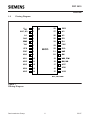
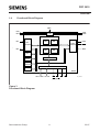
1
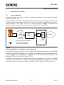
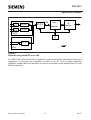
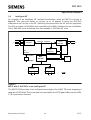
ICs for Communications Mini IOM-2 Controller MICO PEF 2015 Version 1.1 Product Overview 03.97 T2015-XV11-O4-7600 PEF 2015 Revision History: Current Version: Product Overview 03.97 Previous Version:Product Overview 03.96 Page Page (in previous (in new Version) Version) Subjects (major changes since last revision) 5 5 IOM-2 interface supporting 8 IOM-2 channels (old version: 4) - 6 Pinning diagram 10 11 µP interface description updated 10 11 Special functions extendend Edition 03.97 This edition was realized using the software system FrameMaker. Published by Siemens AG, HLSW SYS PD © Siemens AG 1997. All Rights Reserved. Attention please! As far as patents or other rights of third parties are concerned, liability is only assumed for components, not for applications, processes and circuits implemented within components or assemblies. The information describes the type of component and shall not be considered as assured characteristics. Terms of delivery and rights to change design reserved. For questions on technology, delivery and prices please contact the Semiconductor Group Offices in Germany or the Siemens Companies and Representatives worldwide (see address list). Due to technical requirements components may contain dangerous substances. For information on the types in question please contact your nearest Siemens Office, Semiconductor Group. Siemens AG is an approved CECC manufacturer. Packing Please use the recycling operators known to you. We can also help you – get in touch with your nearest sales office. By agreement we will take packing material back, if it is sorted. You must bear the costs of transport. For packing material that is returned to us unsorted or which we are not obliged to accept, we shall have to invoice you for any costs incurred. Components used in life-support devices or systems must be expressly authorized for such purpose! Critical components1 of the Semiconductor Group of Siemens AG, may only be used in life-support devices or systems2 with the express written approval of the Semiconductor Group of Siemens AG. 1 A critical component is a component used in a life-support device or system whose failure can reasonably be expected to cause the failure of that life-support device or system, or to affect its safety or effectiveness of that device or system. 2 Life support devices or systems are intended (a) to be implanted in the human body, or (b) to support and/or PEF 2015 Table of Contents Page 1 1.1 1.2 1.3 1.4 Overview . . . . . . . . . . . . . . . . . . . . . . . . . . . . . . . . . . . . . . . . . . . . . . . . . . . . .4 Features . . . . . . . . . . . . . . . . . . . . . . . . . . . . . . . . . . . . . . . . . . . . . . . . . . . . . .5 Pinning Diagram . . . . . . . . . . . . . . . . . . . . . . . . . . . . . . . . . . . . . . . . . . . . . . . .6 Logic Symbol . . . . . . . . . . . . . . . . . . . . . . . . . . . . . . . . . . . . . . . . . . . . . . . . . .7 Functional Block Diagram . . . . . . . . . . . . . . . . . . . . . . . . . . . . . . . . . . . . . . . .8 2 2.1 2.2 2.3 2.4 Functional Description . . . . . . . . . . . . . . . . . . . . . . . . . . . . . . . . . . . . . . . . .9 IOM-2 Interface . . . . . . . . . . . . . . . . . . . . . . . . . . . . . . . . . . . . . . . . . . . . . . . .9 Serial PCM Interface . . . . . . . . . . . . . . . . . . . . . . . . . . . . . . . . . . . . . . . . . . .10 Microprocessor Interface . . . . . . . . . . . . . . . . . . . . . . . . . . . . . . . . . . . . . . . .11 Special Functions . . . . . . . . . . . . . . . . . . . . . . . . . . . . . . . . . . . . . . . . . . . . . .11 3 3.1 3.2 Application Examples . . . . . . . . . . . . . . . . . . . . . . . . . . . . . . . . . . . . . . . . .12 Access Network . . . . . . . . . . . . . . . . . . . . . . . . . . . . . . . . . . . . . . . . . . . . . . .12 Intelligent NT . . . . . . . . . . . . . . . . . . . . . . . . . . . . . . . . . . . . . . . . . . . . . . . . .14 4 Package Outlines . . . . . . . . . . . . . . . . . . . . . . . . . . . . . . . . . . . . . . . . . . . . .16 Semiconductor Group 3 03.97 PEF 2015 Overview 1 Overview The Mini IOM-2 Controller MICO (PEF 2015) is an interface controller optimized for small line card applications or Intelligent NTs. It is derived from the EPIC core. The MICO supports up to 16 analog subscribers (up to 8 using the SLICOFI) or up to 8 ISDN-BA subscribers. The MICO is used as an interface device on linecards between the subscriber circuits and the network. Therefore it provides one IOM-2 interface for connection of up to 8 ISDN-BA subscribers or up to 16 analog subscribers (up to 8 using the SLICOFI).The MICO also provides one PCM interface for connection to the main system. Additionally the MICO is used to control the subscriber circuits via the C/I and monitor channel as specified in the IOM-2 specification. A parallel µP interface is provided for device programming. Furthermore the MICO contains a nonblocking switching unit with a flexible time slot assignment between the IOM-2 and the PCM interface. The MICO may substitute the EPIC (PEB 2055) or EPIC-S (PEB 2054) in applications that deal with a maximum number of 8 ISDN or 16 analog (8 using the SLICOFI) subscribers connected via one IOM-2 port. The MICO will be fabricated using SIEMENS advanced CMOS technology and will be available in a P-DSO-28 package. Semiconductor Group 4 03.97 Mini IOM-2 Controller MICO PEF 2015 Product Overview for the Version 1.1 1.1 CMOS Features Functions • Interface controller between IOM-2 and PCM for up to 8 ISDN-BA or 16 analog subscribers (up to 8 analog subscribers using the SLICOFI) • B-channel (64 kbit/s) and D-channel (16 kbit/s) switching P-DSO-28 • Configurable Interface (1 port) - Configurable for IOM-, SLD- and PCM-applications - Programmable clock shift - Single or double data clock • PCM interface (1 port) - Freely programmable time slot assignment to up to 128 PCM time slots - Tristate control signal for external driver - Single or double data clock • C/I-channel Handler with a 9-Byte FIFO • Buffered Monitor Handler with a 16-Byte FIFO • Data rate adaption by a programmable PCM clock rate up to 8.192 MHz (single or double data rate) • 7-bit hardware timer General • • • • Siemens/Intel or Motorola type µP interface Supply Voltage: 5 V Extended temperature range -40°C to +85°C P-DSO-28 package Type Ordering Code PEF 2015 Semiconductor Group Package P-DSO-28 5 03.97 PEF 2015 Overview 1.2 Pinning Diagram V DD ALE, A0 1 28 RES 2 27 A3 A1 3 26 A2 RxD 4 25 DD TSC 5 24 DU TxD 6 23 FSC PFS 7 22 DCL PDC 8 21 INT AD0 9 20 CS AD1 10 19 WR, R/W AD2 11 18 RD, DS AD3 12 17 AD7 AD4 13 16 AD6 AD5 14 15 V SS MICO MIC_PINN.DRW Figure 1 Pinning Diagram Semiconductor Group 6 03.97 PEF 2015 Overview 1.3 Logic Symbol V V DD SS FSC PFS DCL PDC DU TxD MICO PEF 2015 DD TSC RxD AD7..AD0 A3..A0 RD (DS) CS WR (R/W) INT RES par_log1.drw Figure 2 Logic Symbol Semiconductor Group 7 03.97 PEF 2015 Overview 1.4 Functional Block Diagram RES FSC DCL PFS PDC Timing upstream (TRANSMIT) DU CM CFI Interface TxD DM downstream (RECEIVE) PCM Interface TSC RxD DD CM DM C/I Monitor access control Sync. Transfer µP interface Timer MICO AD7..AD0 A3..A0 RD WR CS INT (DS) (R/W) mic_blk3.drw Figure 3 Functional Block Diagram Semiconductor Group 8 03.97 PEF 2015 Functional Description 2 Functional Description 2.1 IOM-2 Interface The integrated CFI is a one port serial interface. It comprises two serial data lines (upstream DU and downstream DD), a data clock input or output DCL and a frame sync input or output FSC in IOM-applications. The clock frequency is either equal to the data rate or twice the data rate. The CFI can be configured to data rates up to 8.192 Mbit/s. The CFI is typically used in IOM-2 or SLD configuration to connect layer-1 devices. Figure 4 shows the IOM-2 Interface structure in Line Card Mode: Figure 4 IOM-2 Frame Structure with 2.048 Mbit/s Data Rate The MICO allows the access to all 32 time slots, i.e. 8 IOM-channels, within a frame. The device therefore can handle up to 8 ISDN subscribers or up to 16 analog subscribers (8 using the SLICOFI). Additionally the MICO contains a C/I- and MONITOR-handler to process the C/I- and MONITOR-channels of the IOM-2 protocol. Semiconductor Group 9 03.97 PEF 2015 Functional Description 2.2 Serial PCM Interface The PCM interface formats the data transmitted or received at the PCM-highways. It consists of one port comprising a data receive (RxD), a data transmit (TxD) and an output tristate indication line (TSC). The PCM interface is supplied with a frame signal (PFS) and a PCM clock (PDC). Data rates up to 8.192 Mbit/s are supported. To properly clock the PCM interface a PDC signal with a frequency equal or twice the data rate has to be applied to the MICO. The IOM-2 time slots can be assigned to any of the PCM time slots and vice versa. Any PCM sub time slot can be switched to any of the 4 possible D-channel positions at the IOM-2 interface. In that way up to the 4 D-channels can be handled within one PCM time slot. Figure 5 shows an example of switching 8 B-channels from the IOM-2 interface to 8 consecutive PCM time slots. Furthermore the 4 D-channels are concatenated and switched to the next PCM time slot after the B-channels. IOM-2 8 kHz ch 3 ch 4 ch 5 ch 6 2.048 Mbit/s PCM 8 kHz ts 127 ts 0 8.192 Mbit/s 9 time slots Figure 5 Example of Switching IOM-2 channels to consecutive PCM Time Slots In principle every B-channel may be assigned to any PCM time slot. One D-channel may occupy a single PCM time slot as well. Note: Frame delay is controlled by appropriate programming of switching paths (refer to EPIC User’s Manual). Semiconductor Group 10 03.97 PEF 2015 Functional Description 2.3 Microprocessor Interface The MICO supports Siemens/Intel and Motorola type microprocessors. In the Siemens/ Intel type µP interface either a multiplexed or a demultiplexed bus structure may be chosen. The interface type is selected by pulling up or down two address pins (A1, A0) during the reset state. Pulling-up the appropriate pins selects the Motorola type µP interface, fixing them to ground chooses the Siemens/Intel type µP interface mode. In case of a multiplexed Siemens/Intel bus structure address pin A0 takes over the ALE functionality. The microprocessor interface consists of the following lines: • • • • • • Data Bus, 8-bit wide, D7..D0 Address bus, 4-bit wide, A3..A0 Chip select, CS Two read/write control lines: RD and WR (Intel mode) or DS and R/W (Motorola mode) Interrupt, INT Reset, RES D0-7 A 0-3 DS R/W CS MICO with Motorola Type Interface D 0-7 MICO A 0-3 RD WR CS with Siemens/Intel Type Interface, Demultiplexed Address/Data Bus ALE MICO AD0-7 RD WR CS with Siemens/Intel Type Interface, Multiplexed Address/Data Bus BUS_INTF.DRW Figure 6 Selectable Bus Interface Structures 2.4 Special Functions – Synchronous transfer. This utility allows the synchronous µP-access to two independent channels on the PCM- or CFI-interface. Interrupts are generated to indicate the appropriate access windows. – 7-bit hardware timer. The MICO offers one hardware timer. It can be used to cyclically interrupt the CPU, to determine the double last look period or to generate a proper CFI-multiframe synchronization signal. – Frame length checking. The PFS-period is internally checked against the programmed frame length. Semiconductor Group 11 03.97 PEF 2015 Application Examples 3 Application Examples 3.1 Access Network Access Networks are used in order to connect subscribers to the telecom network quickly and at low cost. One possibility is to use the existing cable TV network to provide telephony services. An existing hybrid fiber-coaxial network (HFCN) that has been upgraded for upstream communication is the basis for such an Access Network. Figure 7 illustrates the functional model of an optical access network (Fiber In The Loop FITL). Master Headend HFCN UIE HFCN Main Distribution Frame HFCN Core Network OLT Digital Local Exchange HFCN: Hybrid Fiber-Coaxial Network OLT: Optical Line Termination UIE: User Interface Equipment Figure 7 Functional Model of an Optical Access Network The master headend will serve one or multiple main distribution frames. Via the HFCN the UIE is provided. Depending on the number of supported user ports and how far the fiber is available, the configuration is called Fiber To The Home (FTTH), Fiber To The Building (FTTB) or Fiber To The Curb (FTTC). The MICO can be used in a configuration where a maximum of 16 POTS or 8ISDN subscribers are needed, e.g. FTTH or FTTB applications. Figure 8 shows an example of an user interface equipment (UIE) providing two POTS and one ISDN subscriber. Semiconductor Group 12 03.97 PEF 2015 Application Examples HV SLIC SLICOFI HV SLIC SLICOFI IOM-2 PCM MICO Tuner Modulation RF Interface 2 POTS mC IEC-Q ISDN Figure 8 Example using the MICO in an UIE The MICO will replace the EPIC in applications where only a few subscribers have to be supported. It connects the subscriber circuits to the HF unit providing switching capability. Additionally the subscriber circuits are controlled via the implemented C/I- and Monitor-Handlers. Semiconductor Group 13 03.97 PEF 2015 Application Examples 3.2 Intelligent NT An example of an Intelligent NT (network termination) using the MICO is shown in figure 9. This gives the ability to connect up to 16 analog (8 using the SLICOFI) subscribers via a t/r line to the NT. Switching functions within the NT are not supported. The PLL provides a 4.096 MHz clock required by the IOM-2 interface in Line Card Mode. This 4.096 MHz clock is derived from the available 1.536 MHz NT clock. SBCX PEB 2081 S IOM-2 TE, 1.536 MHz IEC-Q PEB 2091 U ICC PEB 2070 INTC PEB 8191 1.536 MHz MICO PLL mC PEF 2015 4.096 MHz IOM-2, 4.096 MHz SLICOFI SLICOFI HV-SLIC HV-SLIC t/r t/r Figure 9 MICO with 2 SLICOFIs in an Intelligent NT The MICO PCM port has to be configured according to the IOM-2 TE mode supplying a data rate of 768 kbit/s.This is the data rate used within the NT. Figure 10 shows the IOM2 TE mode frame structure. Semiconductor Group 14 03.97 PEF 2015 Application Examples Figure 10 IOM-2 Terminal Mode Frame Structure As the SLICOFIs are tied to the B1-channels two IOM-2 channels are needed on the IOM port. These have to be switched to the B1- or B2-channel at the PCM port configured as IOM TE mode. The possible time slot assignments are depicted in figure 11. m IOM B1 B2 Channel 0 MON0 IOM D C/I0 MR IC1 IC2 MX Channel 1 MON1 IOM C/I1 MR Channel 2 C/I2 MX Figure 11 Time Slot Assignment in the Intelligent NT using the MICO with 2 SLICOFIs Semiconductor Group 15 03.97 PEF 2015 Package Outlines 4 Package Outlines P-DSO-28 (Plastic Dual Small Outline) Sorts of Packing Package outlines for tubes, trays etc. are contained in our Data Book “Package Information”. SMD = Surface Mounted Device Semiconductor Group 16 Dimensions in mm 03.97