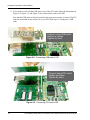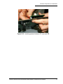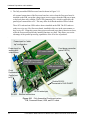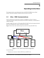
1
PowerQUICC MDS Platform I/O
Board
User Manual
Document Number: Order# (no /D)
Rev. #
09/08/2005
How to Reach Us:
Home Page:
www.freescale.com
E-mail:
support@freescale.com
USA/Europe or Locations Not Listed:
Freescale Semiconductor
Technical Information Center, CH370
1300 N. Alma School Road
Chandler, Arizona 85224
+1-800-521-6274 or +1-480-768-2130
support@freescale.com
Europe, Middle East, and Africa:
Freescale Halbleiter Deutschland GmbH
Technical Information Center
Schatzbogen 7
81829 Muenchen, Germany
+44 1296 380 456 (English)
+46 8 52200080 (English)
+49 89 92103 559 (German)
+33 1 69 35 48 48 (French)
support@freescale.com
Japan:
Freescale Semiconductor Japan Ltd.
Headquarters
ARCO Tower 15F
1-8-1, Shimo-Meguro, Meguro-ku,
Tokyo 153-0064, Japan
0120 191014 or +81 3 5437 9125
support.japan@freescale.com
Asia/Pacific:
Freescale Semiconductor Hong Kong Ltd.
Technical Information Center
2 Dai King Street
Tai Po Industrial Estate
Tai Po, N.T., Hong Kong
+800 2666 8080
support.asia@freescale.com
For Literature Requests Only:
Freescale Semiconductor Literature Distribution Center
P.O. Box 5405
Denver, Colorado 80217
1-800-521-6274 or 303-675-2140
Fax: 303-675-2150
LDCForFreescaleSemiconductor@hibbertgroup.com
Information in this document is provided solely to enable system and software implementers to use
Freescale Semiconductor products. There are no express or implied copyright licenses granted
hereunder to design or fabricate any integrated circuits or integrated circuits based on the information
in this document.
Freescale Semiconductor reserves the right to make changes without further notice to any products
herein. Freescale Semiconductor makes no warranty, representation or guarantee regarding the
suitability of its products for any particular purpose, nor does Freescale Semiconductor assume any
liability arising out of the application or use of any product or circuit, and specifically disclaims any
and all liability, including without limitation consequential or incidental damages. “Typical” parameters
that may be provided in Freescale Semiconductor data sheets and/or specifications can and do vary
in different applications and actual performance may vary over time. All operating parameters,
including “Typicals”, must be validated for each customer application by customer’s technical experts.
Freescale Semiconductor does not convey any license under its patent rights nor the rights of others.
Freescale Semiconductor products are not designed, intended, or authorized for use as components
in systems intended for surgical implant into the body, or other applications intended to support or
sustain life, or for any other application in which the failure of the Freescale Semiconductor product
could create a situation where personal injury or death may occur. Should Buyer purchase or use
Freescale Semiconductor products for any such unintended or unauthorized application, Buyer shall
indemnify and hold Freescale Semiconductor and its officers, employees, subsidiaries, affiliates, and
distributors harmless against all claims, costs, damages, and expenses, and reasonable attorney
fees arising out of, directly or indirectly, any claim of personal injury or death associated with such
unintended or unauthorized use, even if such claim alleges that Freescale Semiconductor was
negligent regarding the design or manufacture of the part.
Freescale™ and the Freescale logo are trademarks of Freescale Semiconductor, Inc. All other
product or service names are the property of their respective owners.
© Freescale Semiconductor, Inc. 2005. All rights reserved.
Section 1
General Information
1.1
1.2
1.3
1.4
1.5
1.6
1.7
Introduction . . . . . . . . . . . . . . . . . . . . . . . . . . . . . . . . . . . . . . . . . . . . . . . . . . . . . . . . . . . . 3
Definitions, Acronyms, and Abbreviations . . . . . . . . . . . . . . . . . . . . . . . . . . . . . . . . . . . . 4
Related Documentation . . . . . . . . . . . . . . . . . . . . . . . . . . . . . . . . . . . . . . . . . . . . . . . . . . . 4
1.3.1 Freescale Documentation . . . . . . . . . . . . . . . . . . . . . . . . . . . . . . . . . . . . . . . . . . . . 4
1.3.2 Third Party Documentation . . . . . . . . . . . . . . . . . . . . . . . . . . . . . . . . . . . . . . . . . . 4
Specifications . . . . . . . . . . . . . . . . . . . . . . . . . . . . . . . . . . . . . . . . . . . . . . . . . . . . . . . . . . . 4
PowerQUICC MDS Platform I/O Board Features . . . . . . . . . . . . . . . . . . . . . . . . . . . . . . 5
PIB General Views . . . . . . . . . . . . . . . . . . . . . . . . . . . . . . . . . . . . . . . . . . . . . . . . . . . . . . 6
Block Diagram . . . . . . . . . . . . . . . . . . . . . . . . . . . . . . . . . . . . . . . . . . . . . . . . . . . . . . . . . . 8
Section 2
Hardware Preparation and Installation
2.1
2.2
Unpacking Instructions . . . . . . . . . . . . . . . . . . . . . . . . . . . . . . . . . . . . . . . . . . . . . . . . . . 11
Installation Instructions . . . . . . . . . . . . . . . . . . . . . . . . . . . . . . . . . . . . . . . . . . . . . . . . . . 11
2.2.1 Preparing the 8Xxx Processor Board: . . . . . . . . . . . . . . . . . . . . . . . . . . . . . . . . . 12
Section 3
Operating Instructions
3.1
3.2
3.3
3.4
83xx - PMC Communications . . . . . . . . . . . . . . . . . . . . . . . . . . . . . . . . . . . . . . . . . . . . . 19
I/O Expander . . . . . . . . . . . . . . . . . . . . . . . . . . . . . . . . . . . . . . . . . . . . . . . . . . . . . . . . . . 20
3.2.1 Register Descriptions . . . . . . . . . . . . . . . . . . . . . . . . . . . . . . . . . . . . . . . . . . . . . . 20
3.2.2 Command Flow . . . . . . . . . . . . . . . . . . . . . . . . . . . . . . . . . . . . . . . . . . . . . . . . . . 21
PCI Logic for PCB Connections . . . . . . . . . . . . . . . . . . . . . . . . . . . . . . . . . . . . . . . . . . . 21
JTAG Connection . . . . . . . . . . . . . . . . . . . . . . . . . . . . . . . . . . . . . . . . . . . . . . . . . . . . . . 22
Section 4
Memory Map
4.1
4.2
Functional Blocks Overview . . . . . . . . . . . . . . . . . . . . . . . . . . . . . . . . . . . . . . . . . . . . . . 25
Functional Blocks Listing . . . . . . . . . . . . . . . . . . . . . . . . . . . . . . . . . . . . . . . . . . . . . . . . 26
Freescale Semiconductor PowerQUICC MDS Platform I/O Board User’s Manual
1
2
PowerQUICC MDS Platform I/O Board User’s Manual Freescale Semiconductor
1
General Information
1.1
Introduction
This document describes the PowerQUICC MDS Platform I/O Board (the PIB).
The PowerQUICC MDS Platform I/O Board, together with the MPC8349E MDS Processor
Board, form the MPC8349E Modular Development System (MDS). The MDS enables
software programmers to develop software for the 8Xxx architecture.
The PIB provides more capabilities for developing 8Xxx software than the MPC83xx Processor
Board alone by allowing an MPC83xx MDS Processor Board to be configured as a Host, with up
to three 8Xxx Processor Boards as Agents, connected to PCI slots on the PIB motherboard.
The PIB also allows an MPC83xx MDS Processor Board to be used in a back plane configuration,
and provides room and connections for an additional USB board.
Power is provided by the PIB, which also provides additional signal connections via the back
plane (if used), and optical GETH connectors on the front plane side of the PIB. The
PowerQUICC MDS Platform I/O Board can be connected to a PC in this configuration (via a
parallel port connector), without the need for an external command converter.
Freescale Semiconductor PowerQUICC MDS Platform I/O Board User’s Manual
3
General Information
1.2
Definitions, Acronyms, and Abbreviations
MDS
Modular Development System
PIB
Platform I/O Board
USB
Universal Serial Bus
GETH
Gigabit Ethernet
PC
IBM-compatible Personal Computer
TCA
PCI
PMC
XMC
ATM
Asynchronous Transfer Mode
BCSR
PHY
Physical Layer
RMII
1.3
Related Documentation
1.3.1
Freescale Documentation
•
•
•
MPC83xx HW Specification
MPC83xx User’s Manual
900 MHz Low Voltage LVPECL Clock Synthesizer (Mar, 2003, Ver. 3)
1.3.2
•
1.4
Third Party Documentation
PCA9555 Data Sheet (2002 Jul. 26) by Philips
Specifications
The PowerQUICC MDS Platform I/O Board specifications are given in Table 1-1.
4
PowerQUICC MDS Platform I/O Board User’s Manual Freescale Semiconductor
General Information
Table 1-1. PowerQUICC MDS Platform I/O Board specifications
CHARACTERISTICS
Power requirements
SPECIFICATIONS
5V @ 3A external DC power supply
No extra power supply for PCI Add-in-Card & PIB
combined modes.
Processor capability
All processors in the 8Xxx line:
• One as host (Processor Board)
• One USB card (optional)
• Up to three 8Xxx cards as agents (optional),
four if using the PIB Expansion Board
Operating temperature
0OC - 70OC
Storage temperature
-25OC to 85OC
Relative humidity
5% to 90% (non-condensing)
Dimensions (nominal, without additional cards):
Length
Width
Height
315 mm
290mm
23mm
1.5
•
•
•
•
•
•
•
PowerQUICC MDS Platform I/O Board Features
Advanced TCA form factor
Operates from a TCA chassis (back plane), or standalone
Four sets of PMC connectors (between PIB and Processor Board) for PCI and QE
functions:
- Each PMC connector set contains an XMC connector for high frequency signals
- Three sets contain PCI signals
- QE signals are split between two sets of PMC connectors
- Two of the four sets of PMC connectors can run simultaneous signals to two ATM
modules; one of the ATM modules has ADTEC connectors
Two PCI buses--PCI1 and PCI2:
- PCI1 operates as a 32bit PCI (on three PMC slots) or as a 64bit PCI (on one PMC slot
- if using the 8349 as agent, this must be slot #2)
- PCI2 operates as 32bit PCI (on two PMC slots)
RS422 port
Eight octal 10/100 Ethernet PHYs with RMII interface
Two 10/100/1000 Ethernet PHYs ports with fiber connectors (copper options are connected
only to the backplane)
Freescale Semiconductor PowerQUICC MDS Platform I/O Board User’s Manual
5
General Information
•
•
•
•
•
•
•
•
1.6
I2C for BCSR read and write
USB1.1 port
8Xxx clock synthesizer
Logic analyzer connectors for all QE signals
Expansion connector for micro-TCOM. This enables a connection to the TCOM
Parallel port interface to host computer; convert to JTAG
Single 48V input power supply (TCA input connector (ZONE-1))
Backplane connectors (ZD Zone-2) for high-speed signals (e.g., 10/100/1000 Base-T)
PIB General Views
Figure 1-1 below presents a general view of the PIB, without any additional cards. The
connections to the back plane are on the bottom, and note the optical GETH connections on the
top right.
Figure 1-1 The PowerQUICC MDS Platform I/O Board with no other boards installed
6
PowerQUICC MDS Platform I/O Board User’s Manual Freescale Semiconductor
General Information
Figure 1-2 below shows a different view of the PIB, this time with a Processor Board, a USB card,
and three PCI cards installed. The agent 8Xxx cards, which can be inserted into the slot on a PCI
card, are not shown.
Power input for “tabletop” configuration
Power input for
working with
a back plane
PCI cards installed
Front plane connection
(optical GETH)
Back plane connection
(incl GETH and voltage)
USB card installed
Clock
Synthesizer
(SW1)
Parallel port
to PC
Double RS-232
connected to RJ45 DUART
RS-422
GETH twisted pair
Ethernet connections
Figure 1-2 PowerQUICC MDS Platform I/O Board External Connections
(Agent 8Xxx boards not installed)
Freescale Semiconductor PowerQUICC MDS Platform I/O Board User’s Manual
7
General Information
1.7
Block Diagram
A schematic block diagram of the PowerQUICC MDS Platform I/O Board is shown in the figure
below. Note that an 8Xxx Processor Board is shown in the shaded area, but this is not an integral
part of the PIB.
8x10/100
RMII
26Pin Header
Parallel Port
10Pin Header
RS422
ZD
Connector
JB22
RS422
Buffer
ZD
Connector
JB23
-48V Input
ZD
Connector
JB24
From
Backplane
RS422
MDC&MDIO
ENET1,2,3,8
ENET6,7
I2C
ENET5
8PinHeader
TSEC1
8PinHeader
TSEC1
IO Expander
ENET4
8xRMII PHY
System Board
I2C
Parallel Port
to JTAG
PCI2/PCI1H
QE Signals
UTOPIA
PCI1L/UPC2
2x OPTIC
USB2
QE Signals
UPC1
MDC,MDIO,SPI,I2C
Bus
Switch
USB1.1
48V to
+3.3V
48V to
+12V
26[0,1]
-48V Input From
External Power Supply
Local Bus
SPARE
Clock
ENET6,7
48V to
+12V
IO Expander
Clock
Synthesizer
RISER CONNECROTS
48V to
+5V
JTAG PMC
BUS SWITCH
26[0,3] 26[0,2]
BUS SWITCH
26[0,0]
J02
J04
J12
J14
J22
J24
J32
J34
J01
J03
J11
J13
J21
J23
J31
J33
J05
J06
J15
J16
J25
J26
J35
J36
PMC1
PMC0
PMC2
PMC3
2xGETH OPTIC
USB1.1
CONN
MINI AB
Figure 1-3 PowerQUICC MDS Platform I/O Board Block Diagram
8
PowerQUICC MDS Platform I/O Board User’s Manual Freescale Semiconductor
General Information
Freescale Semiconductor PowerQUICC MDS Platform I/O Board User’s Manual
9
General Information
10
PowerQUICC MDS Platform I/O Board User’s Manual Freescale Semiconductor
Hardware Preparation and Installation
2
Hardware Preparation and Installation
This chapter provides unpacking instructions, hardware preparation, and installation instructions
for the PowerQUICC MDS Platform I/O Board. For more details on hardware preparation, see the
“Getting Started” document for the PowerQUICC MDS Platform I/O Board.
2.1
Unpacking Instructions
NOTE
If the shipping carton is damaged upon receipt,
request carrier’s agent to be present during
unpacking and inspection of equipment.
CAUTION
AVOID
TOUCHING
AREAS
OF
INTEGRATED
CIRCUITRY;
STATIC
DISCHARGE CAN DAMAGE CIRCUITS.
1. Unpack equipment from shipping carton.
2. Refer to packing list and verify that all items are present.
3. Save packing material for storing and reshipping of equipment.
2.2
Installation Instructions
Do the following in order to install the PowerQUICC MDS Platform I/O Board properly:
•
Verify that Jumpers and Switches are in default positions. For default positions, see the
“Getting Started” document for the PowerQUICC MDS Platform I/O Board.
Freescale Semiconductor PowerQUICC MDS Platform I/O Board User’s Manual
11
Hardware Preparation and Installation
2.2.1
Preparing the 8Xxx Processor Board:
1. Remove protective covers from the 300-pin connectors on the bottom side of the processor board (See Figure 2-1).
2. Remove protective covers from the 300-pin connectors on the PIB board (see Figure 2-2).
Underside of
system board
Remove protective
cover by hand
Figure 2-1 Remove Protective Covers from 300-pin connectors
(underside of 8Xxx Processor Board shown)
Protective Covers
Figure 2-2 Remove Protective Covers from 300-pin connectors
12
PowerQUICC MDS Platform I/O Board User’s Manual Freescale Semiconductor
Hardware Preparation and Installation
Press down to fasten
Figure 2-3 Connect 8Xxx Processor Board to PIB and press down with fingers
3. Connect processor board to PIB board as shown in Figure 2-3.
4. Ensure a tight fit by pressing down on the processor board by hand only until the pins
engage (see Figure 2-3 )
5. Manually fasten the four screws as shown in Figure 2-4.
Figure 2-4 Fasten the four tightening screws
Freescale Semiconductor PowerQUICC MDS Platform I/O Board User’s Manual
13
Hardware Preparation and Installation
6. If you will be working with a back plane, and wish GETH signals to traverse either the
back plane connection, or the front plane optical connection, connect the two GETH
sockets on the Processor Board with sockets on the PIB board as shown in Figure 2-5 and
Figure 2-6.
Note that if you do not do this, you can still connect GETH cables directly to the Processor
board’s sockets, if they are accessible in your laboratory configuration.
Processor Board on PIB
GETH Sockets
GETH Interconnecting
Cables
Figure 2-5 Insert GETH interconnecting cables to GETH sockets on Processor board
14
PowerQUICC MDS Platform I/O Board User’s Manual Freescale Semiconductor
Hardware Preparation and Installation
GETH Interconnecting
Cable connected
Figure 2-6 Connect GETH interconnecting cables to sockets on PIB
7. If you are not working with either the USB or the PCI cards, and you will be working with
the PIB in a “table-top” configuration (as opposed to inserting it in a rack to use its back
plane connections), you can at this point connect the power supply to the voltage input as
shown in Figure 2-7.
Power
Figure 2-7 Connecting Power input to the PIB
Freescale Semiconductor PowerQUICC MDS Platform I/O Board User’s Manual
15
Hardware Preparation and Installation
8. If you wish to work with the USB card, or any of the PCI cards, follow the illustrations in
Figure 2-8, Figure 2-9, and Figure 2-10 to connect these cards to the PIB.
Note that the USB card can only be inserted in the upper-most section, as shown. The PCI
card can be inserted in any section, for up to 4 PCI cards (up to 3 if using also a USB
card).
Connect using USB card’s
latches as shown
Tighten by hand
Figure 2-8 Connecting USB card to PIB
Connect using PCI card’s
latches as shown
Tighten by hand
Figure 2-9 Connecting PCI card to PIB
16
PowerQUICC MDS Platform I/O Board User’s Manual Freescale Semiconductor
Hardware Preparation and Installation
Figure 2-10 Inserting spacers between PCI card and PIB
Freescale Semiconductor PowerQUICC MDS Platform I/O Board User’s Manual
17
Hardware Preparation and Installation
9. The fully assembled PIB-Processor board is shown in Figure 2-11.
All external connections of the Processor board are active when the Processor board is
installed on the PIB, except the voltage input (receives power from the PIB power input,
or the back plane only), and the JTAG/COP connection (P9), which is replaced by the
parallel port connection to a PC. This may differ for different models of 8Xxx boards.
Three PCI cards and one USB card are shown installed on the PIB. The PCI cards are
ready to receive any 83xx Processor board, installed in this case in the same manner as
they are in a PC. Using this system, these processor boards (up to three) function as slaves,
while the Processor board already installed functions as a host. This allows you to take
advantage of the parallel processing capabilities of the 83xx line of products.
.
Power input for “tabletop” configuration
Power input for
working with
a back plane
PCI cards installed
Front plane connection
(optical GETH)
Back plane connection
(incl GETH and voltage)
USB card installed
Clock
Synthesizer
Parallel port
to PC
Double RS-232
connected to RJ45 DUART
RS-422
GETH twisted pair
Ethernet connections
Figure 2-11 Fully Assembled Combined system:
PIB, Processor Board, USB, and PCI cards
18
PowerQUICC MDS Platform I/O Board User’s Manual Freescale Semiconductor
Operating Instructions
3
Operating Instructions
This chapter describes some fundamentals of how the MPC8349E MDS Processor Board
operates. Information regarding communications and controls is provided.
3.1
83xx - PMC Communications
The 83xx chip has two PCI ports (PCI1 and PCI2), in addition to a QE port. In order to
communicate properly with four cards connected to four PMC connections, a certain amount of
control is necessary.
In order to enable this control, an I/O Expander (Philip PCA9555) has been incorporated onto the
PIB. This I/O Expander also controls various blocks on the PIB.
Figure 3-1 below shows the connection logic between the 83xx chip and the PMC slots:
83xx
QE port
PCI-1 port
PCI-2 port
Communications Logic
I/O
Expander
PMC-0
PMC-1
PMC-2
PMC-3
Figure 3-1 83xx - PMC Communication Configurations
Note the following:
•
The QE port can connect to either the PMC0 slot or the PMC1 slot.
Freescale Semiconductor
MPC8349E MDS Processor Board User’s Manual
19
Operating Instructions
•
•
•
•
The PCI1 port can connect to either the PMC1, PMC2, or PMC3 slots. This port can connect
to PMC1, or PMC1/2, or PMC 1/2/3 simultaneously, depending on user configuration, at the
32 bit rate. However, if using a 64 bit rate, the PCI1 port can only connect to the PMC2 slot.
The PCI2 port can connect to either the PMC2 or PMC3 slots. This port can connect to either
PMC2, or PMC 2/3 simultaneously, depending on user configuration, at the 32 bit rate.
A PMCx slot cannot have two different ports connecting to it at the same.
A single JTAG chain is always maintained no matter how many PCB cards are inserted into
the PIB.
Each PMC slot (IDSEL pin) connects to addresses for the 83xx as follows:
•
•
•
PMC1 to AD17,
PMC2 to AD18, and
PMC3 to AD19.
3.2
I/O Expander
The PCA95555PW I/O expander allows the 83xx to communicate and control more PMC
cards than there are ports available on the 83xx chip. In order to work with the PIB, users
must control this multi-register I/O expander device. A short description of the
PCA9555PW follows (For full details on how the I/O Expander works (Philips PCA9555), see
Philips documentation, listed in Section 1.3.2.)
3.2.1
Register Descriptions
The PCA9555PW device is split to two identical parts: 1 and 0. Each part has four 8-bit
registers: input, output, polarity inversion, and configuration.
•
•
•
•
20
Input Port:: (Reg. 0 and 1) Input only; reflects the incoming logic level of a pin, regardless of
whether the pin is defined as an input or an output by Register 3.
Output Port: (Reg. 2 and 3) Output only; reflects the outgoing logic levels of the pins defined
as outputs by Registers 6 and 7.
Polarity Inversion: (Reg. 4 and 5) Allows the user to invert the polarity of the Input Port
register data. If a bit in this register is set (written with “1”), the Input Port data polarity is
inverted.
Configuration Port: (Reg. 6 and 7) Configures the directions of the I/O pins. If a bit in this
register is set, the corresponding port pin is enabled as an input with a high impedance output
driver. If a bit in this register is cleared, the corresponding port pin is enabled as an output. At
reset the device’s ports are inputs. Note that there is a 100KOhm pull-up resister at each pin.
MPC8349E MDS Processor Board User’s Manual
Freescale Semiconductor
Operating Instructions
3.2.2
Command Flow
Figure 3-2 below shows the timing of the command flow of the I/O Expander. Note that
the command byte comes immediately after the address byte during a write transmission.
This byte is used as a pointer to determine which of the registers (Reg. No.0-7 as described
above) will be written or read.
1
S
0
2
1
3
0
4
0
5
6
7
8
A2 A1 A0 0
9
1
2
3
4
5
6
7
8
9
1
2
3
4
5
6
7
8
9
A
0
0
0
0
0
0
1
0
A
0.7 0.6 0.5 0.4 0.3 0.2 0.1 0.0 A
1
2
3
4
5
6
7
8
1.7 1.6 1.5 1.4 1.3 1.2 1.1 1.0
R/W
Agent Address
Command Byte
acknowledgment
from agent
Data Port-0
acknowledgment
from agent
Data Port-1
acknowledgment
from agent
Figure 3-2 Command Flow Timing in I/O Expander
Table 3-1. below shows the relationship between the value of the command byte and the
register to which it is pointing.
.
Table 3-1. PCA9555PW Registers
Command Byte Value
3.3
Register
0
Input Port - 0
1
Input Port - 1
2
Output port - 0
3
Output port - 1
4
Polarity Inversion - 0
5
Polarity Inversion - 1
6
Configuration Port - 0
7
Configuration Port - 1
PCI Logic for PCB Connections
In order to connect properly to the PCB boards, the user must configure the I/O Expander in
accordance with the configurations as listed below.
Freescale Semiconductor
MPC8349E MDS Processor Board User’s Manual
21
9
Operating Instructions
Bits on the I/O expander device’s output port register, that are not directly
mentioned, must be given a “1” value.
Note:
— I2C addr 23 configuration register bit 0,6 = bit must be “1” for PCI host
(See Section 4.1 for an explanation of this bit numbering method)
— I2C addr 27 configuration register bit 1,4 = bit must be “0” for PCI host
— I2C addr 26 configuration register bit 0,0 = "0" enables PCI1 64bits
— I2C addr 26 configuration register bit 0,1 = "0" enables PCI2 to PMC
connectors (for PCI2[L] or PCI1[H])
— I2C addr 26 configuration register bit 0,2 = "0" PCI2 to PMC2
— I2C addr 26 configuration register bit 0,3 = "0" PCI1 to PMC2
Set the bits in according with the desired PCI configuration as follow:
•
PCI1 32bits on PMC1:
— I2C addr 27 bit 1,4 = "0"
— I2C addr 23 bit 0,6 = "1"
Note:The two bits must have opposite values at all times.
•
PCI1 32bits on PMC1 and PMC2:
— I2C addr 26 bit 0,0 = "1"
— I2C addr 26 bit 0,2 = "1"
— I2C addr 26 bit 0,3 = "0"
•
PCI1 32bits on PMC1, PMC2 and PMC3:
—
—
—
—
•
I2C addr 26 bit 0,0 = "1"
I2C addr 26 bit 0,1 = "1"
I2C addr 26 bit 0,2 = "0"
I2C addr 26 bit 0,3 = "0"
PCI1 64bit on PMC2 ONLY:
— I2C addr 26 bit 0,0 = "0"
— I2C addr 26 bit 0,1 = "0"
— I2C addr 26 bit 0,3 = "0"
•
PCI2 32bit on PMC3
— I2C addr 26 bit 0,1 = "0"
•
PCI2 32bit on PMC2 and PMC3:
— I2C addr 26 bit 0,1 = "0"
— I2C addr 26 bit 0,2 = "0"
3.4
JTAG Connection
Figure 3-3 below shows the JTAG connection scheme. The logic is controlled by the JTAG2
22
MPC8349E MDS Processor Board User’s Manual
Freescale Semiconductor
Operating Instructions
block (see Chapter 4 for more details on this block). Note that no matter how many boards are
connected to the PMC slots, a single JTAG chain is maintained at all times.
RISER
CONN
PMC0
PMC1
TDI
TDI
TDO
TDO
X2JTAG_TDI0
X2JTAG_TDI0
X2JTAG_TDI
X2JTAG0_EN
X2JTAG1_EN
X2JTAG_TDO0
X2JTAG_TDO1
X2JTAG_TDI1
CONT
PMC3
PMC2
TDI
TDI
TDO
X2JTAG_TDI1
X2JTAG_TDI2
TDO
X2JTAG_TDI2
X2JTAG2_EN
X2JTAG3_EN
X2JTAG_TDO2
X2JTAG_TDO3
X2JTAG_TDIO
Figure 3-3 JTAG Connection Scheme
Freescale Semiconductor
MPC8349E MDS Processor Board User’s Manual
23
Operating Instructions
24
MPC8349E MDS Processor Board User’s Manual
Freescale Semiconductor
Memory Map
4
Memory Map
4.1
Functional Blocks Overview
The functional blocks on the PIB are listed in the table below. These are all controlled by
any one of the four I/O Expanders. Their addresses are indicated in the column labeled
I2C Bus Address. Details on each block can be found in Section 4.2.
The “Sub Address” nomenclature can be explained using this example:
Sub Address: 0,(0:7) & 1,(0:3)
This means that the sub address is referring to Part 0 of the specific I/O Expander, bits 0-7,
and Part 1, bits 0-3. .
Table 4-1. Blocks and Addresses
Block
I2C Bus Address
Sub Address
TCOM
24H
USB1.1
24H, 26H
RS422
27H
1,(5:6)
Clock Synthesizer
27H
0,(0:7) & 1,(0:3)
OC12 (ATM
622Mbps)
27H
1,7
PCI Host
0,(0:7) &1,(0:3)
1,(4:7) &1,1
23H, 27H
1,4 & 0,6
PCI1
26H
0,0 & 0,3
PCI2
26H
0,2
PMC
23H
1,(0:7)
PCI Expander
Control
23H
0,4 & 0,5
JTAG2
23H
0,(0:3)
ETH 10/100
26H
0,(4:7) & 1,0
M66EN
26H
1,2 & 1,(4:6)
ATM
26H
1,3
Freescale Semiconductor
MPC8349E MDS Processor Board User’s Manual
25
Memory Map
4.2
Functional Blocks Listing
Table 4-2. TCOM Address 24H
SUB ADDRESS
FUNCTION
DESCRIPTION
0,0
TCOM_EN_DS3_2
must be “1” to disable the DS3 or enable the T1/E1
0,1
TCOM_EN_DS3_1
0,2
TCOM_EN_TDM8
"0" to enable QE TDMH of the TCOM
0,3
TCOM_EN_TDM7
"0" to enable QE TDMG of the TCOM
0,4
TCOM_EN_TDM1
"0" to enable QE TDMA of the TCOM
0,5
TCOM_EN_TDM2
"0" to enable QE TDMB of the TCOM
0,6
TCOM_EN_TDM3
"0" to enable QE TDMC of the TCOM
0,7
TCOM_EN_TDM4
"0" to enable QE TDMD of the TCOM
1,0
TCOM_EN_TDM5
"0" to enable QE TDME of the TCOM
1,1
TCOM_EN_TDM6
"0" to enable QE TDMF of the TCOM
1,2
ATMEN
bit value is “Don’t care”
1,3
FETHRST
bit value is “Don’t care”
Table 4-3. USB1.1 24H, 26H
SUB ADDRESS
FUNCTION
DESCRIPTION
24H - 1,4
USB_MODE
Select USB host or agent; for agent this bit must be “1".
24H - 1,5
USBVCC-
For USB host (USB_MODE = "0") this bit must be “"0" . If
USB_mode is “1”, this must be “1”.
24H - 1,6
USBLOWSPD-
Logic 1 operates edge rates for full speed. Logic 0 operates edge
rates for low speed.
24H - 1,7
USBEN-
If the USB bus is inactive then the suspended state enables a low
power state. When the suspend pin is active it drives the RCV pin
to a logic 0 state. Both D+ and D– are tri-stated.
26H - 1,1
USB_EN-
"0" enables the USB function on the I/O Board. "1" disables the
USB1.1 and enables ENET4.
Table 4-4. RS422 27H
SUB ADDRESS
FUNCTION
DESCRIPTION
27H - 1,5
RS_422EN
The bit must be "1" for RS422
27H - 1,6
RS_422EN-
The bit must be "0" for RS422
26
MPC8349E MDS Processor Board User’s Manual
Freescale Semiconductor
Memory Map
The Clock Synthesize can also be manually set via SW1 (after reset).
Table 4-5. Clock Synthesizer Control by SW1
Switch #
FUNCTION
8
M0
7
M1
6
M2
5
M3
4
M4
3
M5
2
M6
1
N0
9
N1
10
OE-
Freescale Semiconductor
DESCRIPTION
Select output frequency according to Table 4-6., “Fout = M/N * Fin.
OE =L low stops FOUT in the logic low state (FOUT =L, FOUT =H).
MPC8349E MDS Processor Board User’s Manual
27
Memory Map
Table 4-6. Fout = M/N * Fin
VCO Frequency for a Crystal Interface Frequency of
M
20
21
22
23
24
25
26
27
28
29
30
31
32
33
34
35
36
37
38
39
40
41
42
43
44
45
46
47
48
49
50
51
52
53
54
55
56
57
58
59
60
61
62
28
M[6:0]
0010100
0010101
0010110
0010111
0011000
0011001
0011010
0011011
0011100
0011101
0011110
0011111
0100000
0100001
0100010
0100011
0100011
0100101
0100110
0100111
0101000
0101001
0101010
0101011
0101100
0101101
0101110
0101111
0110000
0110001
0110010
0110011
0110100
0110101
0110110
0110111
0111000
0111001
0111010
0111011
0111100
0111101
0111110
10
12
14
16
18
20
800
Output Frequency for f XTAL =16 MHz and for
N=
1
2
4
8
828
800
400
200
100
896
448
224
812
816
800
1800
1800
1792
MPC8349E MDS Processor Board User’s Manual
50 Mhz
52 Mhz
54Mhz
56 Mhz
58 Mhz
60 Mhz
62 Mhz
64 Mhz
66 Mhz
68 Mhz
70 Mhz
72 Mhz
74 Mhz
76 Mhz
78 Mhz
80 Mhz
82 Mhz
84 Mhz
86 Mhz
88 Mhz
90 Mhz
92 Mhz
94 Mhz
96 Mhz
98 Mhz
100 Mhz
102 Mhz
104 Mhz
106 Mhz
108 Mhz
110 Mhz
112
Freescale Semiconductor
Memory Map
Table 4-6. Fout = M/N * Fin
VCO Frequency for a Crystal Interface Frequency of
M
63
64
M[6:0]
0111111
1000000
10
12
14
1280
1536
1792
16
18
20
Output Frequency for f XTAL =16 MHz and for
N=
1
2
4
8
Table 4-7. OC12 (ATM622) 27H
SUB ADDRESS
27H - 1,7
FUNCTION
ATM622_RESET-
DESCRIPTION
Reset the OC12 ATM module on connectors P20 & P21.
Table 4-8. PCI HOST 23H, 27H
SUB ADDRESS
FUNCTION
DESCRIPTION
27H - 1,4
83XXPCI_HOST-
When PCI1 is the host the bit should be "0" to drive AD17 to the
PMC1 IDSEL pin, and M66EN to the host. When PCI1 is in ATM
mode then IDSEL is in UPC2-ATMRXD12 and M66EN is in UPC2ATMRXD6.
23H - 0,6
83XXPCI_HOST
Must be "1" if PCI1 is in PCI mode. Should always be the opposite
of 27H-1, 4.
Table 4-9. PCI1 26H
SUB ADDRESS
FUNCTION
DESCRIPTION
26H - 0,0
PCI1_64-
To operate PCI1 in 64 bit mode, this bit must be "0"
26H - 0,3
PCI1_PMC2_EN-
To operate PCI1 in 32 bit mode on PMC2, 3, this bit must be "0".
Note: In this case bit 26H-0, 2 should be "1".
Table 4-10. PCI2 26H
SUB ADDRESS
26H - 0,2
FUNCTION
PCI2_PMC2_EN-
Freescale Semiconductor
DESCRIPTION
To operate the PCI2 bit on PMC2-3 the bit must be "0".
Note: In this case bit 26H-0,0 & 0,3 should be "1".
MPC8349E MDS Processor Board User’s Manual
29
Memory Map
Table 4-11. PMC Control 23H
SUB ADDRESS
FUNCTION
DESCRIPTION
23H - 0,0
PMC0_PRESENT00-
23H - 0,1
PMC0_PRESENT01-
23H - 0,2
PMC0_PRESENT10-
23H - 0,3
PMC0_PRESENT11-
23H - 0,4
PMC0_PRESENT20-
23H - 0,5
PMC0_PRESENT21-
23H - 0,6
PMC0_PRESENT30-
23H - 0,7
PMC0_PRESENT31-
PMC card types, according to specific card used.
Table 4-12. PCI Expander Control 23H
SUB ADDRESS
FUNCTION
DESCRIPTION
23H - 0,4
CONTROL_OUT
Controls 83xx PCI expander board power.
23H - 0,5
CONTROL_IN
Reads the power status of the 83xx PCI expander board.
Table 4-13. JTAG2 23H
SUB ADDRESS
FUNCTION
DESCRIPTION
23H - 0,0
X2JTAG0_EN
If the bit is set to "1" then PMC1 is connected to the JTAG chain; if
the bit is "0" then the PMC1 JTAG is bypassed.
23H - 0,1
X2JTAG1_EN
If the bit is set to "0" then PMC0 is connected to the JTAG chain; if
the bit is "0" then the PMC0 JTAG is bypassed.
23H - 0,2
X2JTAG2_EN
If the bit is set to "0" then PMC2 is connected to the JTAG chain; if
the bit is "0" then the PMC2 JTAG is bypassed.
23H - 0,3
X2JTAG3_EN
If the bit is set to "0" then PMC3 is connected to the JTAG chain; if
the bit is "0" then the PMC3 JTAG is bypassed.
Table 4-14. Ethernet 10/100 26H
SUB ADDRESS
FUNCTION
DESCRIPTION
26H - 0,4
EN_RMIICLKEVEN
The bit must be 1” to enable clock to UCC(2,4,6,8) for Fast Ethernet
RMII.
26H - 0,5
EN_RMIICLKODD
The bit must be 1” to enable clock to UCC (1,3,5,7) for Fast
Ethernet RMII.
26H - 0,6
EN_RMIICLK
OE to the clock oscillator of the 10/100RMII to enable external clock
from PMC0.
30
MPC8349E MDS Processor Board User’s Manual
Freescale Semiconductor
Memory Map
Table 4-14. Ethernet 10/100 26H
SUB ADDRESS
FUNCTION
DESCRIPTION
26H - 0,7
ENET7_EN-
The bit as 0 enables ENET7 for RMII.
Note: Enet7 signals muxed with ATMUPC1 ADDRESS & TDMH.
For ENET7 to enable UPC1 it won’t be able to operate in multi-phy;
TDMH should be disabled.
26H - 1,0
ENET6_EN-
The bit as 0 enables ENET6 for RMII.
Note: ENET6 signals muxed with ATMUPC1.
27H - 1,6
RS_422EN-
The bit as 0 enables RS422. For ENET5 RMII the bit should be "1".
24H - 1,7
USB_EN-
The bit as 0 enables USB1.1. For ENET4 RMII the bit should be
"1".
Table 4-15. M66EN 26H
SUB ADDRESS
26H - 1,2
FUNCTION
PLD_M66EN0
DESCRIPTION
This is the I/O Expander input from PMC1 through the bus switch.
If PCI is not muxed with UPC2 then the I/O Expander reads the bit
as 1--meaning PMC1 has a card with PCI 66Mhz.
When PCI is muxed with UPC2 then there should be a decision
based on processor board mode: if in PCI mode, the ATM_M66EN
signal should be taken; if in ATM mode, the XUPC2_RXD6_M66EN
should be taken.
26H - 1,4
PLD_M66EN2
If the I/O Expander reads the bit as 1 then the PMC2 has a card with
PCI 66Mhz.
26H - 1,5
PLD_M66EN3
If the I/OI/O Expander reads the bit as 1 then the PMC3 has a card
with PCI 66Mhz.
26H - 1,6
XME66
The SW should read PLD_M66EN0, PLD_M66EN2, PLD_M66EN3
and then, by setting the bit, drive the bit to the PCI M66EN signals.
SW should make the decision (0 or 1).
26H - 1,3
ATM_M66EN
If PCI/ATM and ATM are selected then the bit must be "0".
Freescale Semiconductor
MPC8349E MDS Processor Board User’s Manual
31
Memory Map
32
MPC8349E MDS Processor Board User’s Manual
Freescale Semiconductor