1
PCI-1002 Series
Includes PCI-1002L/1002H/1002LU/1002HU
and PEX-1002L/1002H
User Manual
Version 2.8
Oct. 2011
Warranty
All products manufactured by ICP DAS are warranted against defective
materials for a period of one year from the date of delivery to the original
purchaser.
Warning
ICP DAS assumes no liability for damages consequent to the use of this product.
ICP DAS reserves the right to change this manual at any time without notice.
The information furnished by ICP DAS is believed to be accurate and reliable.
However, no responsibility is assumed by ICP DAS for its use, nor for any
infringements of patents or other rights of third parties resulting from its use.
Copyright
Copyright © 2011 by ICP DAS. All rights are reserved.
Trademark
Names are used for identification only and may be registered trademarks of their
respective companies.
PCI-1002 Series User Manual (Ver.2.8, Oct. 2011, PMH-015-28)
1
Tables of Contents
1.
INTRODUCTION................................................................................................................................ 4
1.1
THE BLOCK DIAGRAMS ...................................................................................................... 5
1.2
FEATURES......................................................................................................................... 6
1.3
SPECIFICATIONS ................................................................................................................ 7
1.3.1
PCI-1002L/H and PCI-1002LU/HU..................................................................................... 7
1.3.2
PEX-1002L/H......................................................................................................................... 8
1.3.3
Analog Input Range .............................................................................................................. 9
1.3.4
A/D Trigger Methods............................................................................................................. 9
1.3.5
Interrupt Channel ................................................................................................................ 10
1.3.6
Programmable Timer/Counter........................................................................................... 10
1.4
APPLICATIONS ................................................................................................................. 11
1.5
PRODUCT CHECK LIST ..................................................................................................... 12
2.
3.
HARDWARE CONFIGURATION .................................................................................................. 13
2.1
BOARD LAYOUT ............................................................................................................... 13
2.2
JUMPER SETTINGS .......................................................................................................... 15
2.3
A/D CALIBRATION ............................................................................................................ 16
2.4
CARD ID SWITCH............................................................................................................. 17
2.5
SYSTEM BLOCK ............................................................................................................... 18
2.6
DAUGHTER BOARDS ........................................................................................................ 19
2.6.1
DB-1825 ............................................................................................................................... 19
2.6.2
DB-8225 ............................................................................................................................... 19
2.6.3
DB-37 .................................................................................................................................... 19
2.6.4
DN-37.................................................................................................................................... 20
2.6.5
DB-16P Isolated Input Board............................................................................................. 20
2.6.6
DB-16R Relay Board ......................................................................................................... 21
2.7
ANALOG INPUT SIGNAL CONNECTIONS .............................................................................. 22
2.8
PIN ASSIGNMENTS ........................................................................................................... 26
SOFTWARE INSTALLATION ....................................................................................................... 28
3.1 SOFTWARE INSTALLING PROCEDURE...................................................................................... 28
3.2 PNP DRIVER INSTALLATION ................................................................................................... 29
3.3 CONFIRM THE SUCCESSFUL INSTALLATION ............................................................................. 30
4. I/O REGISTER ADDRESS .................................................................................................................. 31
PCI-1002 Series User Manual (Ver.2.8, Oct. 2011, PMH-015-28)
2
4.1 HOW TO FIND THE I/O ADDRESS............................................................................................. 31
4.2 THE I/O ADDRESS MAP ......................................................................................................... 33
4.2.1
Section 1............................................................................................................................... 34
4.2.3
Section 2.............................................................................................................................. 35
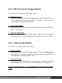
5. FUNCTION OPERATIONS.................................................................................................................. 40
5.1 DIGITAL I/O........................................................................................................................... 40
5.2 THE 8254 TIMER ................................................................................................................... 41
5.3 THE A/D TRIGGER................................................................................................................. 41
5.4 A/D CONVERSION ................................................................................................................. 43
5.4.1
A/D Conversion Trigger Modes......................................................................................... 45
5.4.2
A/D Transfer Modes............................................................................................................ 45
5.4.3
Software Triggers and Polling Techniques ..................................................................... 46
6. SOFTWARE AND DEMO PROGRAM .............................................................................................. 49
6.1
DEMO PROGRAMS FOR WINDOWS .................................................................................... 49
6.2
DEMO PROGRAMS FOR DOS............................................................................................ 50
6.3
DIAGNOSTIC PROGRAM .................................................................................................... 51
6.3.1 Power-ON Plug & Play Test................................................................................................... 51
6.3.2 Driver Plug & Play Test .......................................................................................................... 51
6.3.3 DIO Test.................................................................................................................................... 52
6.3.4 A/D Test .................................................................................................................................... 52
6.4
PIO_PISO.EXE FOR WINDOWS ...................................................................................... 53
PCI-1002 Series User Manual (Ver.2.8, Oct. 2011, PMH-015-28)
3
1. Introduction
The PCI-1002LU/HU and PEX-1002LU/HU cards are the new generation product
that ICP DAS provides to meet RoHS compliance requirement and is designed as
completely compatible with the PCI-1002L/H. Users can replace the PCI-1002L/H
by the PCI-1002LU/HU and PEX-1002LU/HU directly without software/driver
modification.
The PCI-1002L/H supports 5 V PCI bus and PCI-1002LU/HU supports 3.3 V/5 V
PCI bus, while the PEX-1002L/H supports PCI Express bus. The PCI-1002 series
is a family of AD board and features low-gain 110 kS/s or high-gain 44 kS/s
analog input. It provides 12-bit 32 single-ended analog input channels or 16
differential analog input channels, 16 digital input channel and 16 digital output
channel.
The PCI-1002LU/HU and PEX-1002L/U provide pull-high/low jumpers allow user
to predefine the DI status instead of floating when the DI channels are
unconnected or broken. The PEX-1002L/H adds a Card ID switch for users to
recognize the board by the ID via software when using two or more PEX-1002L/H
cards in one computer.
PCI-1002LU/HU (Universal PCI version) and PEX-1002L/H (PCI Express) is fully
compatible with the PCI-1002L/H (PCI version). PCI-1002LU/HU and PEX1002L/H (new version) sell now; PCI-1002L/H (old version) will be phase out.
These cards support various OS such as Linux, DOS, Windows 98/NT/2000 and
32/64-bit Windows 7/Vista/XP. DLL and Active X control together with various
language sample program base on Turbo C++, Borland c++, Microsoft C++,
Visual C++, Borland Delphi, Borland C++ Builder, Visual Basic, C#.NET, Visual
Basic.NET and LabVIEW are provided in order to help users to quickly and easily
develop their own applications.
PCI-1002 Series User Manual (Ver.2.8, Oct. 2011, PMH-015-28)
4
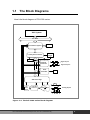
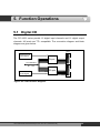
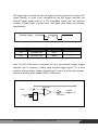
1.1
The Block Diagrams
Here’s the block diagram of PCI-1002 series:
X86 System
PCI BUS
PCI Interface System
EPROM
Status
Control
Local System Controller
Interrupt
Digital Inputs
16 bits DI
16 bits DO
Pacer
Generator
Digital Outputs
4MHz
A/D control logic
A/D
Data
Buffer
12-bit A/D
Converter
Gain
Mux
Analog Inputs
Figure 1-1: The PCI-1002 series block diagram.
PCI-1002 Series User Manual (Ver.2.8, Oct. 2011, PMH-015-28)
5
1.2
Features
The following is a list of general features for the PCI-1002 series. Check section
1.3 for more details.
Bus: 5 V PCI (Peripherals Component Interface) bus for PCI-1002L/H
Universal PCI card, supports both 5 V and 3.3 V PCI bus for PCI-1002LU/HU
PCI Express card, supports PCI Express x1 for PEX-1002L/H
Card ID function for PEX-1002L/H
1. A/D:
The sampling rate of single channel or multiple channels is 110 kS/s. for low
gain model and 44 kS/s. for high gain model.
32 single-ended / 16 differential programmable inputs.
Provides three different A/D trigger methods.
Provides three different external trigger methods.
Programmable gain control, programmable offset control.
2. DIO:
16 digital inputs and 16 digital outputs (TTL compatible).
High speed data transfer rate: 2.7 M word/sec (non-burst mode).
Digital input port can be set to pull-high or pull-low (PCI-1002 LU/HU and
PEX-1002L/H only).
3. Timer:
One 16-bit machine independent timer for software (Timer 2).
Two 16-bit pacer timers for A/D converter and interrupt (Timer0, Timer1).
PCI-1002 Series User Manual (Ver.2.8, Oct. 2011, PMH-015-28)
6
1.3
1.3.1
Specifications
PCI-1002L/H and PCI-1002LU/HU
Model Name
Analog Input
Channels
A/D Converter
Sampling Rate (max.)
FIFO Size
Over voltage Protection
Input Impedance
Trigger Modes
Data Transfer
Accuracy
Zero Drift
Digital Input
Channels
Compatibility
Input Voltage
Response Speed
Digital Output
Channels
Compatibility
Output Voltage
Output Capability
Response Speed
Timer/Counter
Channels
Resolution
Compatibility
Input Frequency
Reference Clock
General
Bus Type
Data Bus
Card ID
I/O Connector
Dimensions(L x W x D)
Power Consumption
Operating Temperature
Storage Temperature
Humidity
PCI-1002L
PCI-1002H
PCI-1002LU
PCI-1002HU
32 single-ended/16 differential
12-bit, 8 µs Conversion time
110 kS/s.
44 kS/s.
110 kS/s.
44 kS/s.
N/A
Continuous +/-35 Vp-p
10 MΩ/6 pF
Software, Internal programmable pacer,
External (5 V/TTL compatible)
Polling, Interrupt
0.01 % of FSR ±1 LSB @ 25 °C, ± 10 V
+/-4 ppm/°C of FSR
16
5 V/TTL
Logic 0: 0.8 V max. ; Logic 1: 2.0 V min.
1.0 MHz (Typical)
16
5 V/TTL
Logic 0: 0.4 V max. ; Logic 1: 2.4 V min.
Sink: 2.4 mA @ 0.8 V ; Source: 0.8 mA @ 2.0 V
1.0 MHz (Typical)
3(Independent x 1/Internal pacer x 1/External pacer x 1)
16-bit
5 V/TTL
10 MHz max.
Internal: 4 MHz
5 V PCI, 32-bit, 33 MHz
3.3 V / 5 V Universal PCI, 32-bit
16-bit
No
Female DB37 x 1 ; 20-pin box header x 2
175 mm x 105 mm x 22 mm
188 mm x 105 mm x 22 mm
960 mA @ +5 V
0 ~ 60 °C
-20 ~ 70 °C
5 ~ 85% RH, non-condensing
PCI-1002 Series User Manual (Ver.2.8, Oct. 2011, PMH-015-28)
7
1.3.2
PEX-1002L/H
Model Name
Analog Input
Channels
A/D Converter
Sampling Rate (max.)
FIFO Size
Over voltage Protection
Input Impedance
Trigger Modes
Data Transfer
Accuracy
Zero Drift
Digital Input
Channels
Compatibility
Input Voltage
Response Speed
Digital Output
Channels
Compatibility
Output Voltage
Output Capability
Response Speed
Timer/Counter
Channels
Resolution
Compatibility
Input Frequency
Reference Clock
General
Bus Type
Data Bus
Card ID
I/O Connector
Dimensions(L x W x D)
Power Consumption
Operating Temperature
Storage Temperature
Humidity
PEX-1002L
PEX-1002H
32 single-ended/16 differential
12-bit, 8 µs Conversion time
110 kS/s.
44 kS/s.
N/A
Continuous +/-35 Vp-p
10 MΩ/6 pF
Software, Internal programmable pacer,
External (5 V/TTL compatible)
Polling, Interrupt
0.01 % of FSR ±1 LSB @ 25 °C, ± 10 V
+/-4 ppm/°C of FSR
16
5 V/TTL
Logic 0: 0.8 V max. ; Logic 1: 2.0 V min.
500 kHz
16
5 V/TTL
Logic 0: 0.4 V max. ; Logic 1: 2.4 V min.
Sink: 2.4 mA @ 0.8 V ; Source: 0.8 mA @ 2.0 V
500 kHz
3(Independent x 1/Internal pacer x 1/External pacer x 1)
16-bit
5 V/TTL
10 MHz max.
Internal: 4 MHz
PCI Express x 1
16-bit
Yes (4-bit)
Female DB37 x 1 ; 20-pin box header x 2
188 mm x 105 mm x 22 mm
800 mA @ +5 V
0 ~ 60 °C
-20 ~ 70 °C
5 ~ 85% RH, non-condensing
PCI-1002 Series User Manual (Ver.2.8, Oct. 2011, PMH-015-28)
8
1.3.3
Analog Input Range
Analog Input Range:
Model
PCI-1002 L/LU and PEX-1002L (Low-Gain)
Gain
Bipolar
Sampling Rate
(Max.)
Model
1
2
4
8
+/- 10
+/- 5
+/- 2.5
+/- 1.25
110 kS/s.
110 kS/s.
110 kS/s.
110 kS/s.
PCI-1002 H/HU and PEX-1002H (High-Gain)
Gain
Bipolar
Sampling Rate
(Max.)
1.3.4
1
10
100
1000
+/-10
+/- 1
+/- 0.1
+/- 0.01
44 kS/s.
36 kS/s.
7 kS/s.
0.8 kS/s.
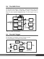
A/D Trigger Methods
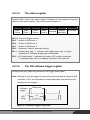
Trigger methods:
Software trigger.
Pacer trigger: 16-bit programmable timer/counter.
External trigger: Pre-trigger, Post-trigger, external Pacer trigger.
Pacer or software trigger
External trigger
CHn
CHn
t
Start
End
Normal trigger mode
Start
End
t
Post-trigger mode
External trigger
External trigger
CHn
CHn
Start
End
External pacer trigger mode
t
Start
End
t
Pre-trigger mode
Figure 1-2: Trigger methods of PCI-1002 series.
PCI-1002 Series User Manual (Ver.2.8, Oct. 2011, PMH-015-28)
9
1.3.5
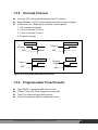
Interrupt Channel
Interrupt: INTA (Automatically assigned by PCI-initiator).
Enable/Disable: Via PCI control register and add-on control register.
Interrupt source: (Selected by on-board control register)
1. A/D conversion interrupt.
2. Pacer 0 interrupt (Timer 0).
3. Pacer 1 interrupt (Timer 1).
4. External interrupt.
1.
End of Conversion
2.
Pacer 0
A/D busy
IRQ
IRQ
3.
Falling edge of Pacer 0
Falling edge of Pacer 1
Falling edge of
4.
External trigger
Pacer 1
External
Trigger
IRQ
IRQ
Figure 1-3: Programmable interrupt source.
1.3.6
Programmable Timer/Counter
Type: 82C54 -8 programmable timer/counter.
Timers: Timer 0 for Pacer triggers and interrupts.
Timer 1 for External trigger and interrupt.
Timer 2 for software machine independent timer.
PCI-1002 Series User Manual (Ver.2.8, Oct. 2011, PMH-015-28)
10
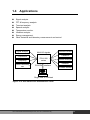
1.4
Applications
Signal analysis.
FFT & frequency analysis.
Transient analysis.
Speech analysis.
Temperature monitor.
Vibration analysis.
Energy management.
Other industrial and laboratory measurement and control.
Signal Analysis
Multi-I/O signals
Transition
Temperature
Frequency
Other Laboratory
use
Process Control
PCI-1002
series
Speech Analysis
Vibration
PCI/PEX Interface
Process Monitor
Single-task or multitask
Figure 1-4: PCI-1002 series multifunction cards.
PCI-1002 Series User Manual (Ver.2.8, Oct. 2011, PMH-015-28)
11
1.5
Product Check List
The shipping package includes the following items:
One PCI-1002 series card as follows:
•
PCI-1002L/PCI-1002H
•
PCI-1002LU/PCI1002HU
•
PEX-1002L/PEX-1002H
One software utility PCI CD.
One Quick Start Guide
It is recommended that you read the Quick Start Guide first. All the
necessary and essential information is given in the Quick Start Guide, including:
Where to get the software driver, demo programs and other resources.
How to install the software.
How to test the card.
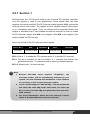
Attention!
If any of these items is missing or damaged, contact the dealer from whom
you purchased the product. Please save the shipping materials and carton
in case you need to ship or store the product in the future.
PCI-1002 Series User Manual (Ver.2.8, Oct. 2011, PMH-015-28)
12
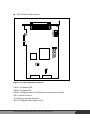
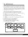
2. Hardware Configuration
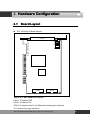
2.1
Board Layout
PCI-1002LU/HU Board Layout:
CON3
VR2
JP1 VR1 VR3
PCI-1002LU/HU REV:B
CON1
CON2
Figure 2-1: PCI-1002 board layout.
CON1: 16-channel D/O
CON2: 16-channel D/I
CON3: 32 single-ended or 16 differential analog input channels
JP1: Analog input type selection
PCI-1002 Series User Manual (Ver.2.8, Oct. 2011, PMH-015-28)
13
PEX-1002L/H Board Layout:
Figure 2-2: PEX-1002 board layout.
CON1: 16-channel D/O
CON2: 16-channel D/I
CON3: 32 single-ended or 16 differential analog input channels
SW1: Card ID function.
JP1: Analog input type selection
JP2: Pull-high/pull-low jumper for D/I
PCI-1002 Series User Manual (Ver.2.8, Oct. 2011, PMH-015-28)
14
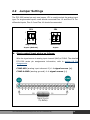
2.2
Jumper Settings
The PCI-1002 series has only one jumper. JP1 is used to select the analog input
type. For single-ended inputs, users should connected Pins 1-3 and Pins 2-4. For
differential inputs, Pins 3-5 and Pins 4-6 should be connected.
JP1
JP1
1
2
1
2
5
6
5
6
Single-ended
Differential
Inputs (Default)
Inputs
Single-ended Input wiring as follows:
Wire the signal source to analog input channel 0(AI0) of CON3. The detailed
PCI-1002 series pin assignments information, refer to section 2.8 Pin
Assignments.
CON3.AI0 (analog input channel 0) ÅÆ signal source (+)
CON3.A.GND (analog ground) ÅÆ signal source (-)
PCI-1002 Series User Manual (Ver.2.8, Oct. 2011, PMH-015-28)
15
Differential Input wiring as follows:
Wire the signal source to analog input channel 0(AI0) of CON3. The detailed
PCI-1002 series pin assignments information, refer to section 2.8 Pin
Assignments.
CON3.AI0+ (analog input channel 0+) ÅÆ signal source (+)
CON3.AI0- (analog input channel 0-) ÅÆ signal source (-)
2.3
A/D Calibration
AD Calibration for PCI-1002 series card:
Step 1: Apply +10 V to channel 0.
Step 2: Apply +0 V to channel 1.
Step 3: Apply -10 V to channel 2.
Step 4: Run DEMO6.EXE of DOS.
VR1, VR2, VR3
Step 5: Adjust VR1 until channel 0 = fff or ffe
Step 6: Adjust VR2 until channel 1 = 800 or 801
Step 7: Adjust VR3 until channel 2 = 000 or 001
Step 8: Repeat Step 4, Step 5 and Step 6 until all are OK.
PCI-1002 Series User Manual (Ver.2.8, Oct. 2011, PMH-015-28)
16
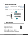
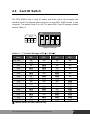
2.4
Card ID Switch
The PEX-1002L/H has a Card ID switch with which users can recognize the
board by the ID via software when using two or more PEX-1002L/H cards in one
computer. The default Card ID is 0x0. For detail SW1 Card ID settings, please
refer to Table 2.1.
NO
ID 2
ID 3
ID 1
ID 0
SW1
1
2
3
4
(Default Settings)
Table 2.1 (*) Default Settings; OFF Æ 1; ON Æ 0
Card ID
1
2
3
(Hex)
ID0
ID1
ID2
(*) 0x0
ON
ON
ON
4
ID3
ON
0x1
OFF
ON
ON
ON
0x2
ON
OFF
ON
ON
0x3
OFF
OFF
ON
ON
0x4
ON
ON
OFF
ON
0x5
OFF
ON
OFF
ON
0x6
ON
OFF
OFF
ON
0x7
OFF
OFF
OFF
ON
0x8
ON
ON
ON
OFF
0x9
OFF
ON
ON
OFF
0xA
ON
OFF
ON
OFF
0xB
OFF
OFF
ON
OFF
0xC
ON
ON
OFF
OFF
0xD
OFF
ON
OFF
OFF
0xE
ON
OFF
OFF
OFF
0xF
OFF
OFF
OFF
OFF
※ Card ID Switch for PEX-1002L/H only
PCI-1002 Series User Manual (Ver.2.8, Oct. 2011, PMH-015-28)
17
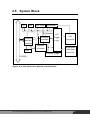
2.5
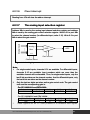
System Block
D/I
8254 Timer
D/O
A/D Buffer
Data
PCI/PEX
Interface
Controller
Adr
Interrupt
controller
A/D
Trigger
Logic
Dispatch
controller
NVRA
External Trigger
A/D
Converter
Multiplexers
, Gain Amp.
Scale Adj.
PCI/PEX
Figure 2-2: PCI-1002 series System Function Block.
PCI-1002 Series User Manual (Ver.2.8, Oct. 2011, PMH-015-28)
18
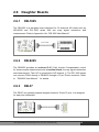
2.6
2.6.1
Daughter Boards
DB-1825
The DB-1825 is a daughter board designed for 32 channels AD cards such as
ISO-AD32 and PCI-1002 series that can easy signal connection and
measurement. Refer to Appendix A for “DB-1825 User Manual”.
37pin cable
2.6.2
DB-8225
The DB-8225 provides an on-board CJC (Cold Junction Compensation) circuit
for thermocouple measurement and a terminal block for easy signal connection
and measurement. The CJC is connected to A/D channel_0. The PCI-1002 series
can connect CON3 directly to DB-8225 through a 37-pin D-sub connector. Refer
to “DB-8225 User Manual" for details.
2.6.3
DB-37
The DB-37 is a general purpose daughter board for D-sub 37 pins. It is designed
for easy wire connection.
PCI-1002 Series User Manual (Ver.2.8, Oct. 2011, PMH-015-28)
19
2.6.4
DN-37
The DN-37 is a general purpose daughter board for DIN Rail Mounting. It is
designed for easy wire connection. It is Din-Rail mounted.
37pin cable
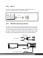
2.6.5
DB-16P Isolated Input Board
The DB-16P is a 16-channel isolated digital input daughter board. The optically
isolated input of the DB-16P consists of a bi-directional optocoupler with a resistor
for current sensing. You can use the DB-16P to sense DC signal from TTL levels
up to 24 V, or use the DB-16P to sense a wide range of AC signals. You can use
this board to isolate the computer from large common-mode voltage, ground
loops and transient voltage spikes that often occur in industrial environments.
Opto-Isolated
R
V+
PCI-1002(H/L) D/I
D/I
V-
20-Pin cable
DB-16P
PCI-1002(H/L)
AC or DC Signal 0V to 24V
PCI-1002 Series User Manual (Ver.2.8, Oct. 2011, PMH-015-28)
20
2.6.6
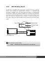
DB-16R Relay Board
The DB-16R, a 16-channel relay output board, consists of 16 Form C relays for
efficient load switching via programmable controls. It is connected and
functionally compatible with 785 series board but feature an industrial-type
terminal block. Relays are energized by applying 5-volt signal to the appropriate
relay channel on the 20-pin flat connector. There are 16 enunciator LEDs for each
relay, light when their associated relay is activated. To avoid overloading your
PC’s power supply, this board provides a screw terminal for an external power
supply.
Normally Open
Form C Relay
Normally Closed
Com.
D/O
20-Pin cable
PCI-1002(H/L) Series
!
DB-16R
Note: Channel: 16 Form C Relay
Relay:
Switching up to 0.5 A at 110 VAC or 1 A at 24 VDC
PCI-1002 Series User Manual (Ver.2.8, Oct. 2011, PMH-015-28)
21
2.7
Analog Input Signal Connections
The PCI-1002 series can measure single-ended or differential-type analog input
signal. Some analog signals can be measured in both modes. However, some
analog signals only can be measured in one or the other. The user must decide
which mode is suitable for measurement.
In general, there are 4 different analog signal connection methods (shown from
Figure 2-3 to Figure 2-6). The connection in Figure 2-3 is suitable for ground
analog input signals. The Figure 2-4 connection is used to measure more
channels than in Figure 2-3, but it is only suitable for analog input signals that
large than 1 V. The connection in Figure 2-5 is suitable for thermocouple and the
Figure 2-6 connection is suitable for floating source analog input signals.
Note: In Figure 2-5, the maximum common mode voltage between the
analog input source and the AGND is 70 Vp-p, so the user must take care
that the input signal is under this specification first. If the common mode
voltage is over 70 Vp-p, the input multiplexer will be permanently damaged!
The simple way to select your input signal connection configuration is listed below.
1. Grounding source input signal Æ select Figure 2-3
2. Thermocouple input signal
Æ select Figure 2-5
3. Floating source input signal
Æ select Figure 2-6
4. If Vin > 0.1 V, the gain<=10 and more channels are
needed
Æ select Figure 2-4
If you are unsure of the characteristics of your input signal, follow these test step:
1. Step1 : Try Figure 2-3 and record the measurement result
2. Step2 : Try Figure 2-6 and record the measurement result
3. Step3 : Try Figure 2-4 and record the measurement result
4. Compare the three results and select the best one
PCI-1002 Series User Manual (Ver.2.8, Oct. 2011, PMH-015-28)
22
Figure 2-3. Connecting to grounding source input (Right way)
A/D CH0 HI
Es 1
A/D CH 0 LO
A.GND 1
A/D CH n HI
Es n
A/D CHn LO
A.GND n
Figure 2-3. Wrong way
A/D CH0HI
Es1
A/D CH0LO
GND1
AGND
A/D CHnHI
Esn
A/D CHnLO
GNDn
AGND
PCI-1002 Series User Manual (Ver.2.8, Oct. 2011, PMH-015-28)
23
Figure 2-4. Connecting to single-ended input configuration
PCI-1002
A/D CH0
A/D CH1
A/D CH n
Es
AGND
Figure 2-5. Connecting to thermocouple configuration
PCI-1002
A/D CH 0 HI
A/D CH 0 LO
A/D CH n HI
A/D CH n LO
A. GND
Do not join LO to A.GND at the computer
Note: If the input signal is not thermocouple, the user should use an oscilloscope
to measure common mode voltage of Vin before connecting to PCI-1002 series.
Don’t use a voltage meter or multimeter.
CAUTION: In Figure 2-5, the maximum common mode voltage
between the analog input source and the AGND is 70 Vp-p. Make sure that the
input signal is under specification first! If the common mode voltage is over
70 Vp-p, the input multiplexer will be permanently damaged.
PCI-1002 Series User Manual (Ver.2.8, Oct. 2011, PMH-015-28)
24
Figure 2-6. Connecting to floating source configuration
PCI-1002
A/D CH 0 HI
Es 1
A/D CH 0 LO
A.GND
A/D CH n HI
Es n
A/D CH n LO
A.GND
Signal Shielding
Signal shielding connections in Figure 2-3 to Figure 2-6 are all the same
Use a single-point connection to frame ground (not A.GND or D.GND)
PCI-1002 series
A.GND
D.GND
Vin
Frame Ground
PCI-1002 Series User Manual (Ver.2.8, Oct. 2011, PMH-015-28)
25
2.8
Pin Assignments
CON1: Digital output connector pin assignments.
CON1
1
3
5
7
9
11
13
15
17
19
DO 0
DO 2
DO 4
DO 6
DO 8
DO 10
DO 12
DO 14
GND
+5V
2
4
6
8
10
12
14
16
18
20
DO 1
DO 3
DO 5
DO 7
DO 9
DO11
DO13
DO15
GND
+12V
Name
Pin
Name
1
Digital output 0
2
Digital output 1
3
Digital output 2
4
Digital output 3
5
Digital output 4
6
Digital output 5
7
Digital output 6
8
Digital output 7
9
Digital output 8 10
Digital output 9
11
Digital output 10 12
Digital output 11
13
Digital output 12 14
Digital output 13
15
Digital output 14 16
Digital output 15
17
PCB ground
18
PCB ground
19
PCB +5 V
20
PCB +12 V
CON2: Digital input connector pin assignments.
CON2
DI 0
DI 2
DI 4
DI 6
DI 8
DI 10
DI 12
DI 14
GND
+5V
Pin
1
3
5
7
9
11
13
15
17
19
2
4
6
8
10
12
14
16
18
20
DI 1
DI 3
DI 5
DI 7
DI 9
DI 11
DI 13
DI 15
GND
+12V
Pin
Name
Pin
Name
1
Digital input 0
2
Digital input 1
3
Digital input 2
4
Digital input 3
5
Digital input 4
6
Digital input 5
17
Digital input 6
8
Digital input 7
9
Digital input 8
10
Digital input 9
11
Digital input 10
12
Digital input 11
13
Digital input 12
14
Digital input 13
15
Digital input 14
16
Digital input 15
17
PCB ground
18
PCB ground
19
PCB +5 V
20
PCB +12 V
PCI-1002 Series User Manual (Ver.2.8, Oct. 2011, PMH-015-28)
26
CON3: Analog input/output connector pin assignment.
CON3
AI 0/0+
AI 1/1+
AI 2/2+
AI 3/3+
AI 4/4+
AI 5/5+
AI 6/6+
AI 7/7+
AI 8/8+
AI 9/9+
AI 10/10+
AI 11/11+
AI 12/12+
AI 13/13+
AI 14/14+
AI 15/15+
A.GND
N.C .
Ext_Trg
!
1
2
3
4
5
6
7
8
9
10
11
12
13
14
15
16
17
18
19
20
21
22
23
24
25
26
27
28
29
30
31
32
33
34
35
36
37
Pin
AI 16/0AI 17/1AI 18/2AI 19/3AI 20/4AI 21/5AI 22/6AI 23/7AI 24/8AI 25/9AI 26/10AI 27/11AI 28/12AI 29/13AI 30/14AI 31/15N.C.
D.GND
Name
S.E.
Diff.
1
AI 0
AI 0+
2
AI 1
3
Pin
Name
S.E.
Diff.
20
AI 16
AI 0-
AI 1+
21
AI 17
AI 1-
AI 2
AI 2+
22
AI 18
AI 2-
4
AI 3
AI 3+
23
AI 19
AI 3-
5
AI 4
AI 4+
24
AI 20
AI 4-
6
AI 5
AI 5+
25
AI 21
AI 5-
7
AI 6
AI 6+
26
AI 22
AI 6-
8
AI 7
AI 7+
27
AI 23
AI 7-
9
AI 8
AI 8+
28
AI 24
AI 8-
10
AI 9
AI 9+
29
AI 25
AI 9-
11
AI 10
AI 10+
30
AI 26
AI 10-
12
AI 11
AI 11+
31
AI 27
AI 11-
13
AI 12
AI 12+
32
AI 28
AI 12-
14
AI 13
AI 13+
33
AI 29
AI 13-
15
AI 14
AI 14+
34
AI 30
AI 14-
16
AI 15
AI 15+
35
AI 31
AI 15-
17
A.GND
36
N.C.
18
N.C.
37
D.GND
19
External trigger
Note:
1. Once differential analog input is selected (JP1 3-5, 4-6), Pins 1-16 will
be assign as the positive inputs while Pins 20-35 will act as the negative
inputs of the channel.
2. ‘ N.C. ’ is short for “Not Connected”.
PCI-1002 Series User Manual (Ver.2.8, Oct. 2011, PMH-015-28)
27
3. Software Installation
The PCI-1002 series can be used in DOS and Windows 98/NT/2K and 32-bit/64bit Windows XP/2003/Vista/7. The recommended installation procedure for
windows is given in Sec. 3.1 ~ 3.3. Or refer to Quick Start Guide
(CD:\NAPDOS\PCI\PCI-1002\ Manual\QuickStart\).
http://ftp.icpdas.com/pub/cd/iocard/pci/napdos/pci/pci-1002/manual/QuickStart/
3.1 Software Installing Procedure
UniDAQ SDK driver (32-bit/64-bit Windows XP/2003/Vista/7):
Step 1: Insert the companion CD into the CD-ROM drive and after a few
seconds the installation program should start automatically. If it
doesn’t start automatically for some reason, double-click the
AUTO32.EXE file in the NAPDOS folder on this CD.
Step 2: Click the item: “PCI Bus DAQ Card”.
Step 3: Click the item: “UniDAQ”.
Step 4: Click the item: “DLL for Windows 2000 and XP/2003/Vista 32-bit”.
Step 5: Double-Click “UniDAQ_Win_Setup_x.x.x.x_xxxx.exe” file in the
Driver folder.
Windows driver (Windows 98/NT/2K and 32-bit Windows XP/2003/Vista/7):
Step 1: Insert the companion CD into the CD-ROM drive and after a few
seconds the installation program should start automatically. If it
doesn’t start automatically for some reason, double-click the
AUTO32.EXE file in the NAPDOS folder on this CD.
Step 2: Click the item: “PCI Bus DAQ Card”.
Step 3: Click the item: “PCI-1002L/H”.
Step 4: Click the item “DLL and OCX for Win95/98/2000/NT”.
Step 5: Choose the Win2K_XP, Win98 or WinNT folders for setup according
to your PC platform and then double-Click “.exe” to install driver.
PCI-1002 Series User Manual (Ver.2.8, Oct. 2011, PMH-015-28)
28
The setup program will then start the driver installation and copy the relevant
files to the specified directory and register the driver on your computer. The
directory where the drive is stoned is different for different windows versions, as
shown below.
Windows 64-bit Windows XP/2003/Vista/7:
The UniDAQ.DLL file will be copied into the C:\WINNT\SYSTEM32 folder
The NAPWNT.SYS and UniDAQ.SYS files will be copied into the
C:\WINNT\SYSTEM32\DRIVERS folder
!
For more detailed UniDAQ.DLL function information, please refer to
UniDAQ SDK user manual (CD:\NAPDOS\PCI\UniDAQ\Manual\).
http://ftp.icpdas.com/pub/cd/iocard/pci/napdos/pci/unidaq/maunal/
Windows NT/2K and 32-bit Windows XP/2003/Vista/7:
The P100X.DLL file will be copied into the C:\WINNT\SYSTEM32 folder
The NAPWNT.SYS and PCI1002.SYS files will be copied into the
C:\WINNT\SYSTEM32\DRIVERS folder
Windows 95/98/ME:
The P100X.DLL and P100X.Vxd files will be copied into the
C:\Windows\SYSTEM folder
!
For more detailed P100X.DLL function information, please refer to
“PCI-1002 Series Software Manual.pdf” (CD:\NAPDOS\PCI\PCI1002\Manual\). http://ftp.icpdas.com/pub/cd/iocard/pci/napdos/pci/pci1002/manual/
3.2 PnP Driver Installation
Power off the computer and install the PCI-1002 series card. Turn on the
computer and Windows 98/ME/2K and 32-bit/64-bit Windows XP/2003/Vista/7
should automatically defect the new PCI device(s) and then ask for the location
of the driver files for the hardware. If a problem is encountered during
installation, refer to the PCI_ISA_PnP_Driver_Installation_in_Win9x_2x_xp.pdf
(CD:\NAPDOS\PCI\Manual\) for more information.
PCI-1002 Series User Manual (Ver.2.8, Oct. 2011, PMH-015-28)
29
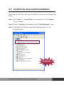
3.3 Confirm the Successful Installation
Make sure the PCI-1002 series cards installed are correct on the computer as
follows:
Step 1: Select “Start” Æ “Control Panel” and then double click the “System”
icon on Windows.
Step 2: Click the “Hardware” tab and then click the “Device Manager” button.
Step 3: Check the PCI-1002 series cards which listed correctly or not, as
illustrated below.
Successful
PCI-1002 Series User Manual (Ver.2.8, Oct. 2011, PMH-015-28)
30
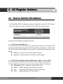
4. I/O Register Address
4.1 How to find the I/O Address
The Plug&Play BIOS will assign a proper I/O address to every PCI-1002 series
cards in the power-on stage. The IDs of PCI-1002 series are as follows:
Model Name
PCI-1002 L/H
PCI-1002 LU/HU
PEX-1002 L/H
Vendor ID
0x1234
Device ID
0x1002
We provide the following necessary functions:
1. P1002_DriverInit(&wBoard)
This function can detect how many PCI-1002 series cards are in the system. The
function is implemented based on the PCI Plug & Play mechanism-1. It will find all
PCI-1002 series cards installed in this system & save all their resources in the
library.
wBoard=1 Æ only one PCI-1002 in this PC system.
wBoard=2 Æ there are two PCI-1002 in this PC system.
2. P1002_GetConfigAddressSpace(wBoardNo, *wBase, *wIrq, *wPLX)
Use this function to save resources of all PCI-1002 installed in this system.
Then the application program can control all functions of PCI-1002 directly.
wBoardNo=0 to N Æ totally N+1 cards of PCI-1002
wBase Æ base address of the board control word
wIrq
Æ allocated IRQ channel number of this board
wPLX Æ base address of PCI-interface-IC
PCI-1002 Series User Manual (Ver.2.8, Oct. 2011, PMH-015-28)
31
Here’s the sample program source code:
/* Step1: Detect all PCI-1002 cards first */
wRetVal=P1002_DriverInit(&wBoards);
printf("Threr are %d PCI-1002 Cards in this PC\n",wBoards);
/* Step2: Save resources of all PCI-1002 cards installed in this PC */
for (i=0; i<wBoards; i++)
{
P1002_GetConfigAddressSpace(i,&wBase,&wIrq,&wPLX);
printf("\nCard_%d: wBase=%x, wIrq=%x, wPLX=%x", i,wBase,wIrq,wPLX);
wConfigSpace[i][0]=wBaseAddress;
/* save all resource of this card */
wConfigSpace[i][1]=wIrq;
/* save all resource of this card */
wConfigSpace[i][2]=wPLX;
/* save all resource of this card */
}
/* Step3: Control the PCI-1002 directly */
wBase=wConfigSpace[0][0];
/* get base address the card_0 */
outpw(wBase+0x20,wDoValue);
/* control the D/O states of card_0 */
wDiValue=inpw(wBase+0x20);
/* read the D/I states of card_0 */
wBase=wConfigSpace[1][0];
/* get base address of card_1 */
outpw(wBase+0x20,wDoValue);
/* control the D/O states of card_1 */
wDiValue=inpw(wBase+0x20);
/* read the D/I states of card_1 */
wPLX=wConfigSpace[2][2];
_outpd(wPLX+0x4c,0x41);
…
…
…
_outpd(wPLX+0x4c,0);
/* get PCI-interface base address of card-2 */
/* channel_1, interrupt active_Low */
/* disable all interrupt
PCI-1002 Series User Manual (Ver.2.8, Oct. 2011, PMH-015-28)
*/
32
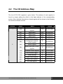
4.2 The I/O Address Map
The list of PCI-1002 registers is given below. The address of each register is
found by simply adding the offset to the base address of the corresponding
section. More detailed descriptions of each register will be shown in the following
text and the software manual.
Section
Offset
Name
Access
Length
1
4ch
PCI interrupt control
register
R/W
8/16/32 bits
00h
8254 timer1
R/W
8/16/32 bits
04h
8254 timer2
R/W
8/16/32 bits
08h
8254 timer3
R/W
8/16/32 bits
0Ch
8254 control register
W
8/16/32 bits
10h
Analog input channel
control register
W
10h
Status register
R
8/16/32 bits
14h
Analog input gain control
register
W
8/16/32 bits
18h
General control register
W
8/16/32 bits
1Ch
A/D software trigger
W
8/16/32 bits
1Ch
Clear Interrupt
R
8/16/32 bits
20h
Digital output register
W
16/32 bits
20h
Digital input register
R
16/32 bits
30h
A/D data register
R
16/32 bits
2
PCI-1002 Series User Manual (Ver.2.8, Oct. 2011, PMH-015-28)
8/16/32 bits
33
4.2.1 Section 1
Although there are 128 I/O ports used by the on-board PCI interface controller,
only one register is used in real applications!! Users should keep the other
registers from being modified! The PCI interrupt control register (4Ch) controls the
interrupt sent to your system. The register is set to “disable interrupt” after poweron or a hardware reset signal. Thus, no interrupt will be generated before this
register is activated even if user enables the add-on interrupt! In order to enable
the PCI-interrupt, always write 43h to this register. Write 03h to this register if you
want to disable the PCI interrupt.
Here’s the format of the PCI interrupt control register:
Bit 31-Bit 7
Bit6
Bit5-Bit3
Bit2
Bit1-Bit0
Not used
Interrupt Enable
Not used
Interrupt Flag
Interrupt Select
Bit 6: Write a ‘1’ to enable the PCI-interrupt and a ‘0’ to disable PCI interrupt.
Bit 2: This bit is readable but can’t be written. A ‘1’ indicates that Add-on has
generated interrupt, ‘0’ means that add-on hasn’t generated interrupt.
Bit 1-0: Always write 1 to these two bits.
!
Note:
1.
Because
PCI-1002
series
supports
“Plug&Play”,
the
interrupt number will be automatically assigned by your
system. Use the standard PCI mechanism or the software
in our library to find out the interrupt number.
2.
If your system supports “Shared IRQ”, several peripherals
will share the same IRQ at the same time. You must use
Bit-2 to find out if this IRQ was generated from your PCI1002 series!!!
3.
For more information about the PCI interrupt control,
refers to the PLX-9050 user reference manual.
PCI-1002 Series User Manual (Ver.2.8, Oct. 2011, PMH-015-28)
34
4.2.3 Section 2
This section is used by the add-on control logic. 64 bytes of I/O locations are
used. Detailed descriptions are shown below.
4.2.3.1
The 8254 registers
The 8254, programmable timer/counter is used to generate periodic A/D trigger
signals, periodic interrupt signals and the machine- independent timer for PCI1002. Addresses 00h, 04h, 08h and 0Ch are used to control the 8254.
Timer 0 is used as Pacer 0. Timer 1 is used as Pacer 1. Timer 2 is used as a
machine-independent timer, P1002_Dealy(). For more details about the
programming information, please refer to Intel’s “Microsystem Components
Handbook”.
4.2.3.2
The DI / DO register
Address 20h is used for DI / DO ports. Writing to this port will write data to DO
register. Reading from this port will read the data from DI.
4.2.3.3
The A/D buffer
Address 30h is used for A/D buffer. Only read operations are available at this
address. Reading from this port will read the data from A/D buffer. The format of
A/D buffer is:
Bit15-12
Analog input channel
Bit11-0
A/D data
Bit 15-12: The channel number of analog input. Only the lower 4 bits of the
channel number are shown in this register.
Bit 11-0: The A/D data.
PCI-1002 Series User Manual (Ver.2.8, Oct. 2011, PMH-015-28)
35
4.2.3.4
The status register
Address 10h is used by the status register. Reading from this address will get the
data from the status register. The format of status register is:
Bit7-6
Bit5
Bit4
Gain
Control
8245
Timer 1
8245
Timer 0
Bit3
Bit2
Bit1
8245
Analog
Reserved
Timer 2
input type
Bit0
A/D ready
Bit 7-6: Current A/D gain control.
Bit 5 : Output of 8254 timer 1.
Bit 4 : Output of 8254 timer 0.
Bit 3 : Output of 8254 timer 2.
Bit 2 : Reserved. Used for hardware testing.
Bit 1 : Analog input type, ‘1’ indicates that analog input type is singleended and ‘0’ indicates analog input is differential.
Bit 0 : A/D ready signal. ‘0’ indicates not ready, A/D is under conversion.
‘1’ indicates ready, A/D is completely converted and is idle now.
4.2.3.5
The A/D software trigger register
Writing to this port (1Ch) will generate an A/D trigger pulse signal.
Note: Although a very fast trigger can be performed (more than the speed of A/D
controller, 110 K) via this method, a reasonable delay time should be left
between the two triggers.
Software
trigger
A/D
Busy
Delay time
8 μs
Conversion Time
Figure 4-1: Software trigger delay time.
PCI-1002 Series User Manual (Ver.2.8, Oct. 2011, PMH-015-28)
36
4.2.3.6
Clear interrupt
Reading from 1Ch will clear the add-on interrupt.
4.2.3.7
The analog input selection register
Address 10h is used by the analog input channel selection register and address
…
Analog inputs
14h is used by the analog gain control selection register. Write 0-31 to port 10h
to select the channel number (for differential input, write 0-15). Write 0-3 to port
14h to select the gain control.
Analog
Mux.
ADC
AMP
Select
Gain control
…
Channel select
Figure 4-2: Analog input control.
Note:
1. For single ended inputs, channels 0-31 are available. For differential inputs,
channels 0-15 are available. Input numbers which are more than the
available channel will be discarded. Thus, for single-ended inputs, only the
last 5 bits are taken as the channel number. And for differential inputs, only
the last 4 bits are taken as the channel number.
2. Only the last two digits are taken as the gain control code. The gain control
code and the corresponding gain is:
For PCI-1002L/LU and PEX-1002L:
Gain code
Gain
[0 0]
1
[0 1]
2
[1 0]
4
[1 1]
8
For PCI-1002H/HU and PEX-1002H:
3.
[Bit1, Bit 0]
[0 0]
[0 1]
[1 0]
[1 1]
Gain
1
10
100
1000
These registers are set to 0 after powered-on or hardware reset signals.
PCI-1002 Series User Manual (Ver.2.8, Oct. 2011, PMH-015-28)
37
4.2.3.8
The general control register
A general control register (18h) is used to control the add-on interrupt signal
source and the A/D trigger method. The format of this register is:
Bit4-2
Bit 1-0
Interrupt source selection
register
A/D trigger method selection register
Interrupt source selection
There are four interrupts selectable for PCI-1002 (refer to section 1.3.5).
[Bit4,Bit3,Bit2]
Descriptions
[ 0, 0, 0 ]
No interrupt source, disable all interrupts.
[ 0, 0, 1 ]
Interrupt after A/D completes conversion.
[ 0, 1, 0 ]
Interrupt after 8254 timer 0 falls.
[ 0, 1, 1 ]
Interrupt after external trigger falls.
[ 1, 0, 0 ]
Interrupt after 8254 timer 1 falls.
Others
No interrupt source, Disable all interrupts.
Note: Bit 2-4 of general control register is set to 0 after hardware reset.
PCI-1002 Series User Manual (Ver.2.8, Oct. 2011, PMH-015-28)
38
Trigger method selection
Here’s a list of our trigger options (refer to section 1.3.4):
[Bit1,Bit0 ]
Descriptions
[ 0, 0 ]
General trigger mode.
8254 timer 0 trigger (internal pacer trigger) or software
trigger.
[ 0, 1 ]
External clock trigger mode.
[ 1, 0 ]
Pre-trigger mode.
[ 1, 1 ]
Post-trigger mode.
Note:
1. In general trigger mode, both 8254 timer 0 and software triggers are treated
as A/D trigger signals. In this mode, 8254 timer 0 and software trigger
should not work at the same time!! This means users should not generate
the software trigger while 8254 timer 0 is activated!!
2.
In external clock trigger mode, external trigger input is taken as the A/D
trigger signal. An event of the external trigger input fall (falling edge) will
generate one A/D trigger.
3.
The pre-trigger mode is used for pre-trigger method. The mode is
incorporated with the 8254 timer 1. First, setup 8254 timer 1 properly. Then
set the trigger mode to pre-trigger. Once pre-trigger mode has been
activated, the 8254 timer 1 will automatically turn on and start to perform
A/D triggers. It will continue until the A/D trigger logic receives a falling
external trigger signal. Any change to the trigger mode selection will turn off
the pre-trigger mode.
4.
The post-trigger mode is used for post-trigger method. The mode working
incorporated with the 8254 timer 1. First, setup 8254 timer 1 properly. Then
set the trigger mode to post-trigger. Once post-trigger mode has been
activated, the 8254 timer 1 will automatically turn off until it receives a falling
external trigger signal. Any change to the trigger mode selection will turn off
the post-trigger mode.
5.
The A/D trigger is set to 0 after either power-on or hardware reset.
PCI-1002 Series User Manual (Ver.2.8, Oct. 2011, PMH-015-28)
39
5. Function Operations
5.1 Digital I/O
The PCI-1002 series provide 16 digital input channels and 16 digital output
channels. All levels are TTL compatible. The connection diagram and block
diagram are given below:
CN2
BaseAddr+20h
read signal.
DI port
Local Data Bus
D0 ... D15
BaseAddr+20h
write signal
DO port
CN1
Figure 5.1: DIO function diagram.
PCI-1002 Series User Manual (Ver.2.8, Oct. 2011, PMH-015-28)
40
5.2 The 8254 Timer
The PCI-1002 series provide 3 independent, 16-bit timer/counters. Each timer
has different functions. Timer 0 is uses Pacer 0. Timer 1 is uses Pacer 1.
Timer 2 is uses a machine independent timer. The block diagram is given as
follows:
VCC
4 M Hz
EN
CLK
Timer0
OUT0
Pacer 0
Local Data
CLK
Bus
Timer1
User
EN
CLK
Timer2
EN
8254
Pacer 1
OUT1
Status
OUT2
Figure 5-2: 8254 control diagram.
5.3 The A/D Trigger
The A/D trigger is controlled by on-board A/D trigger controller.
The function diagram of A/D trigger is shown below:
8254
Timer 0
Software Trigger
0
1
External
Trigger.
PR
D
To A/D
External Trigger
Q
RS
Mux
EN
CLK
8254
Timer 1
4 MHz
Select
Trigger Select
Figure 5-3: A/D trigger controller.
PCI-1002 Series User Manual (Ver.2.8, Oct. 2011, PMH-015-28)
41
A/D trigger logic receives the external trigger and then performs the correct A/D
trigger function. In order to be recognized by the A/D trigger controller, the
external trigger signal must be a TTL compatible signal, with the minimum
duration of pulse width to avoid noise. This signal must satisfy the following
specifications:
External trigger
tdu
tre
Symbol
Name
Minimum
Maximum
Tdu
Duration time
40ns
∞
Tre
Recover time
100ns
∞
Note: The PCI-1002 series is designed only as a time sensitive trigger (trigger
depends only on receiving a falling edge external trigger signal). For a level
sensitive external trigger (trigger depends only on the level of the input signals),
make the following circuit outside the PCI-1002 series:
Comparator
Input
PCI-1002
D/O
External
Trigger
DAC
PCI-1002 Series User Manual (Ver.2.8, Oct. 2011, PMH-015-28)
TTL buffer
42
5.4 A/D Conversion
An A/D conversion can be initiated in one of three ways: software command,
internal programmable interval timer, or by external trigger to the A/D. At the end
of the A/D conversion, it is possible to transfer the data in two ways: by polling a
status register and reading data when ready, or by generating a hardware
interrupt signal to call service routine. All operating modes are selected by a
control register on the PCI-1002 series.
Before using the A/D conversion function, please follow this checklist:
A/D data register (BASE+30h) Æ store the A/D conversion data.
A/D data conversion ready register (BASE +10h) Æ Check A/D conversion
ready.
A/D gain control register (BASE+14h) Æ Select gain.
A/D multiplex control register (BASE+10h) Æ Select analog input
channel.
A/D mode control register (BASE+18h) Æ Select trigger mode and interrupt
source.
A/D software trigger control register (BASE+1Ch).
JP1 to select single-ended or differential input.
3 Trigger logic: Software, Pacer or External trigger.
2 Transfer logic: Polling or Interrupt.
Here’s the block diagram:
16/8 to 1
Multiplexer
Gain
Control
BASE+10h
BASE+14h
CN3
12 bits
A/D
Trigger
Logic
Buffer
BASE+30h
Memory
CPU
BASE+1Ch
Software Trigger
PCI-1002
PCI-1002 Series User Manual (Ver.2.8, Oct. 2011, PMH-015-28)
43
A/D conversion flow:
Before using the A/D converter, please select either single-ended or differential
input (JP1).
The software driver supports two different modes: polling and interrupt. The
user can control the A/D conversion by polling mode very easy. Using the
software driver is recommended if using interrupt.
The multiplexer can select 32 single-ended or 16 differential signals into the gain
control module. The settling time of multiplexer depends on the impedance
of the signal source. Because the software doesn’t control the settling time,
please make sure to leave enough settling time if switching from one
channel to the next channel.
The gain control module also needs settling time if gain control code changed.
Again, because the software doesn’t control settling time, please delay
enough settling time if the gain control code is changed.
Remember to delay the extra setting time when gain of channel is changed.
The software driver provides a machine independent timer, P1002_Delay(), for
settling time delays. This subroutine assumes a machine independent timer will
be implemented. However, if using call P1002_Delay(), the counter 0 will be
reserved and can’t be used as a user programmable timer/counter.
The gain control module’s output feeds into the A/D converter. The A/D
converter needs a trigger signal to start an A/D conversion cycle. The PCI1002 series supports three trigger modes: software, pacer, and external trigger.
PCI-1002 Series User Manual (Ver.2.8, Oct. 2011, PMH-015-28)
44
5.4.1 A/D Conversion Trigger Modes
The PCI-1002 series supports three trigger modes.
1 : Software Trigger :
Write any value to the A/D software trigger control register, BASE+1Ch, and
it will initiate an A/D conversion cycle. This mode is very simple but
controlling the sampling rate very difficult.
2 : Pacer Trigger Mode :
See section 4.2 for a block diagram for this pacer timer. The sample rate of
pacer is very precise.
3 : External Trigger Mode :
When a rising edge of external trigger signal is applied, an A/D conversion
will be performed. The external trigger source comes from Pin-19 of CON3.
5.4.2 A/D Transfer Modes
PCI-1002 series supports two transfer modes.
1 : Polling transfer :
This mode can be used with all trigger modes. You have to disable timer 0
before polling. The software reads the A/D data register from [BASE+30h]
when READY bit of Register [BASE +10h] =1.
2 : Interrupt transfer:
This mode can be used with either a pacer trigger or external. A hardware
interrupt signal is sent to the PC when an A/D conversion is completed.
If using interrupt transfer, it is recommended to use PCI-1002 software
driver.
PCI-1002 Series User Manual (Ver.2.8, Oct. 2011, PMH-015-28)
45
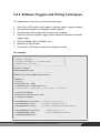
5.4.3 Software Triggers and Polling Techniques
The easiest way to control is by following these steps:
1.
2.
3.
4.
Send 00h to A/D mode control register (software trigger + polling transfer)
Send channel number to multiplexer control register.
Send the gain control code value to gain control register.
Send any value to software trigger control register to generate a software
trigger signal.
5. Scan the READY bit until READY bit =1
6. Read the 12-bit A/D data.
7. Convert this 12-bit binary data to the floating point value.
For example:
/* -------------------------------------------------------------- */
/* DEMO 3: AdPolling
*/
/* Compiler: Borland C++ 3.1, Mode Large
*/
/* Output Code: HEX code
*/
/* -------------------------------------------------------------- */
#include "P1002.H"
WORD wBaseAddr,wIrq;
//------------------------------------------------------WORD P1002_Delay(WORD wDownCount)
{
WORD h,l;
int count;
wDownCount &= 0x7fff;
if (wDownCount<1) wDownCount=1;
/* Clock in=4M --> count 4000 = 1 ms, count 1 = 0.25 us */
l=wDownCount&0xff;
wDownCount=wDownCount / 256;
h=wDownCount&0xff;
outp(wBaseAddr+3*4,0xB0); /* mode_0, counter_2 */
outp(wBaseAddr+2*4,l);
/* counter_2 low byte first */
outp(wBaseAddr+2*4,h);
/* counter_2 high byte ,0x07D0=2000 */
outp(wBaseAddr+3*4,0x80);
l=inp(wBaseAddr+2*4);
h=inp(wBaseAddr+2*4);
/* latch counter_2 */
/* delay starting two CLKs */
PCI-1002 Series User Manual (Ver.2.8, Oct. 2011, PMH-015-28)
46
for (count=32767;count>0;count--)
{
outp(wBaseAddr+12,0x80);
/* latch counter_2 */
l=inp(wBaseAddr+8);
h=inp(wBaseAddr+8);
if (h>=0x80) return NoError;
}
return TimeOut;
}
//-------------------------------------------------------void AdPolling(UCHAR channel, UCHAR gain, WORD delay)
{
outp(wBaseAddr+0x18,0);
// Select Mode 0
outp(wBaseAddr+0x10,channel);
outp(wBaseAddr+0x14,gain);
P1002_Delay(delay);
outp(wBaseAddr+0x1c,01);
// A/D software trigger
}
void SetupTimer(WORD wChannel, WORD wCoef)
{
WORD cmd;
wChannel=wChannel&0x03;
cmd=0x34+(wChannel<<6);
outpw(wBaseAddr+3*4, cmd);
outp(wBaseAddr+wChannel*4, (UCHAR)(wCoef&0xff));
outp(wBaseAddr+wChannel*4, (UCHAR)(wCoef>>8));
}
//===================================================
void main()
{
int i,j;
WORD wBoards,wRetVal,wPLX;
WORD Drdy,wAdData=0;
char c;
clrscr();
P1002_DriverInit(&wBoards);
printf("\n(1) Threr are %d PCI-1002 Cards in this PC",wBoards);
if ( wBoards==0 )
{
putch(0x07); putch(0x07); putch(0x07);
printf("(1) There are no PCI-1002 card in this PC !!!\n"); exit(0);
}
printf("\n(2) Show the Configuration Space of all PCI-1002:");
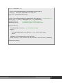
PCI-1002 Series User Manual (Ver.2.8, Oct. 2011, PMH-015-28)
47
for(i=0; i<wBoards; i++)
{
P1002_GetConfigAddressSpace(i,&wBaseAddr,&wIrq,&wPLX);
printf("\n Card_%d: wBaseAddr=%x, wIrq=%x,
wPLX=%x",i,wBaseAddr,wIrq,wPLX);
}
P1002_GetConfigAddressSpace(0,&wBaseAddr,&wIrq,&wPLX); /* select card_0 */
printf("\n(3) *** Card_0, wBaseAddr=%x ***\n",wBaseAddr);
SetupTimer(0,1);
// AdPolling have to disable timer 0
AdPolling(0,0,23);
// channel=0, gain=+/-10, delay=23us
for(i=0;i<10;i++)
{
outp(wBaseAddr+0x1c,01); // A/D software trigger
while(1)
{
if( ((inpw(wBaseAddr+0x10))&0x01)==1) // check if A/D ready?
break;
}
wAdData=((inpw(wBaseAddr+0x30))&0x0fff);
printf("\nRang:+/-10V, Counter %d ,ADC channel 0 value: 0x%xH",i,wAdData);
}
P1002_DriverClose();
}
PCI-1002 Series User Manual (Ver.2.8, Oct. 2011, PMH-015-28)
48
6. Software and Demo Program
6.1
Demo Programs for Windows
Please note that none of the demo programs will work normally if the DLL driver
has not been installed correctly. During the DLL driver installation process, the
install shield will register the correct kernel driver to the operating system and
copy the DLL driver and demo programs to the correct location depending on the
driver software package you have selected (Win98/Me/NT/2000 and 32-bit Win
XP/2003/Visa/7). After installing the driver, the related demo programs,
development library and declaration header files for the different development
environments will be available in the following folders.
The demo program is contained in:
CD:\NAPDOS\PCI\PCI-1002\DLL_OCX\Demo\
http://ftp.icpdas.com/pub/cd/iocard/pci/napdos/pci/pci-1002/dll_ocx/demo/
BCB 4 Æ For Borland C++ Builder4
P100X.H Æ Header files
P1100xbc.LIB Æ Linkage library for
Delphi4 Æ For Delphi 4
P100X.PAS Æ Declaration files
VB6 Æ For Visual Basic 6
P100x.BAS Æ Declaration files
VC6 Æ For Visual C++ 6
P100x.H Æ Header files
P100x.LIB Æ Linkage library for VC6
A list of available demo
programs is as follows:
ChScan_Interrupt demo
ChScan_Pacer demo
ChScan_polling demo
Config demo
DIO demo
Interrupt demo
Pacer demo
Polling demo
VB.NET2005 Æ For VB.NET2005
P100x.vb Æ Declaration files
CSharp2005 Æ For C#.NET2005
P100x.cs Æ Declaration files
PCI-1002 Series User Manual (Ver.2.8, Oct. 2011, PMH-015-28)
49
6.2
Demo Programs for DOS
The related DOS software and demos are located on the CD as below:
CD:\NAPDOS\PCI\PCI-1002\dos\
http://ftp.icpdas.com/pub/cd/iocard/pci/napdos/pci/pci-1002/dos/
After installing the software, the following drivers will be installed onto your hard
disk:
…\1002\BC\LARGE\DEMO>
…\1002\BC\LARGE\LIB>
← demo program
← library and driver
A list of available demo programs is as follows:
DEMO1: Digital output.
DEMO2: Digital output and Digital input test by itself.
DEMO3: ADC Polling for channel 0.
DEMO4: ADC Polling for channel 0,1,2,3 using different gains-1,2,4 or 8.
DEMO5: ADC Pacer trigger.
DEMO6: AD Calibration.
DEMO7: Find card number.
PCI-1002 Series User Manual (Ver.2.8, Oct. 2011, PMH-015-28)
50
6.3
Diagnostic Program
6.3.1 Power-ON Plug & Play Test
The operation steps for a power-on Plug & Play test are as follows:
Step 1: Power-off PC
Step 2: Install PCI-1002 without any extra external connector
Step 3: Power-on PC and check the PC screen very carefully
Step 4: The PC will perform a self-test first
Step 5: Detect the non-PCI physical devices installed in the system
Step 6: Show the information of these device in screen
Step 7: Detect the PCI Plug & Play devices installed in the system
Show all PCI-device information Æ check here carefully
Æ There will be a PCI device with vendor_ID=1234, device_ID=1002 (PCI1002 series)
If the Plug & Play ROM-BIOS detects the PCI-1002 series card during the poweron time, the software driver of DOS, and Windows 95/NT/2000/XP will function
well later. If the Plug & Play ROM-BIOS can’t find the PCI-1002 series, all
software drivers will not function. Therefore the user must make sure that the
power-on procedure is correct.
6.3.2 Driver Plug & Play Test
Step 1: Power-off PC.
Step 2: Install PCI-1002 without any extra external connectors.
Step 3: Power-on PC. Run DEMO7.EXE of DOS.
Step 4: The I/O base address of all PCI-1002 installed in the system will be
shown in screen.
Step 5: Is the total number of boards correct?
Step 6: Install a 20-pin flat cable into one of these PCI-1002 cards.
Step 7: One card’s D/O=D/I Æ This is the physical card number. Remember this
number.
Step 8: Repeat the previous two steps to find the physical card number for each
board.
PCI-1002 Series User Manual (Ver.2.8, Oct. 2011, PMH-015-28)
51
6.3.3 DIO Test
Step 1: Power-off PC.
Step 2: Install one PCI-1002 card with a 20-pin flat cable between CON1 and
CON2.
Step 3: Power-on PC, Then run DEMO2.EXE of DOS.
Step 4: The DO and DI will show either TEST OK or TEST ERROR.
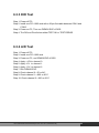
6.3.4 A/D Test
Step 1: Power-off PC.
Step 2: Install one PCI-1002 card.
Step 3: Power-on PC, run DEMO6.EXE of DOS
Step 4: Apply +10V to channel 0.
Step 5: Apply +0V to channel 1.
Step 6: Apply -10V to channel 2.
Step 7: Run DEMO6.EXE.
Step 8: Check channel 0 = fff or ffe?
Step 9: Check channel 1 = 800 or 801?
Step 10: Check channel 2 = 000 or 001?
PCI-1002 Series User Manual (Ver.2.8, Oct. 2011, PMH-015-28)
52
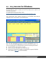
6.4
PIO_PISO.EXE for
Windows
The PIO_PISO.exe utility is located on the CD as below and is useful for all
PIO/PISO series cards.
CD:\NAPDOS\PCI\Utility\Win32\PIO_PISO\
http://ftp.icpdas.com/pub/cd/iocard/pci/napdos/pci/utility/win32/pio_piso/
After executing the utility, detailed information for all PIO/PISO cards that are
installed in the PC will be shown, as illustrated below:
Note: The PIO_PISO.EXE application is valid for all PIO/PISO cards. The
user can execute the PIO_PISO.EXE file to retrieve the following information:
List all PIO/PISO cards installed in the PC
List the resources allocated to each PIO/PISO card
List the Ven_ID and Dev_ID details for identification of specific PIO/PISO
cards. (Refer to Sec. 4.1 for more information)
PCI-1002 Series User Manual (Ver.2.8, Oct. 2011, PMH-015-28)
53