1
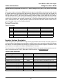
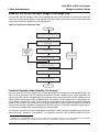
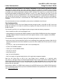
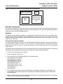
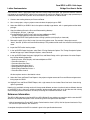
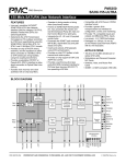
ispLever
CORE
TM
Quad SPI-3 to SPI-4 Link Layer Bridge Core
User’s Guide
October 2005
ipug29_02.0
Quad SPI-3 to SPI-4 Link Layer
Bridge Core User’s Guide
Lattice Semiconductor
Introduction
Lattice’s Quad SPI-3 (System Packet Interface Level 3) to SPI-4 (System Packet Interface Level 4) Bridge is an IP
core which serves as a bridge between one SPI-4 and one to four SPI-3 links.
Lattice’s Quad SPI-3 to SPI-4 Bridge core is a core developed in conjunction with the Lattice ORCA® ORSPI4
FPSC to provide a full solution. For more information on these and other Lattice products, refer to the Lattice web
site at www.latticesemi.com.
This user’s guide explains the functionality of the Quad SPI-3 to SPI-4 Bridge core and how it can be implemented
to provide a full SPI-3 to SPI-4 bridging solution. It also explains how to achieve the maximum level of performance.
The Quad SPI-3 to SPI-4 Bridge core comes with the documentation and the files listed below:
• Data sheet
• Lattice gate level netlist
• ModelSim simulation models and test benches available for free evaluation
• Core instantiation template
Features
• Quad full-featured SPI-3 LINK Interfaces as defined by the OIF specifications
• Supports full clock rates for SPI-3 core: 104MHz
• Each SPI-3 LINK can support up to eight ports
• Seamless integration with the SPI-4.2 Embedded core in the ORSPI4 FPSC
• 10Gbps aggregate throughput
• Parameterizable number of SPI-3 LINK interfaces (1 to 4)
• Parameterizable SPI-3 BYTE_MODE or PKT_MODE selection
• Configurable through MicroProcessor Interface (MPI) ORCA4 System Bus
• Programmable parity type on SPI-3 bus. Default is ODD.
General Description
The Quad SPI-3 to SPI-4 Bridge Intellectual Property (IP) Core targets the programmable array section of the
ORCA ORSPI4 FPSC and provides a bridging function between one to four SPI-3 links and a SPI-4 link.
The ORSPI4 is an FPSC built on the Series 4 re-configurable embedded System-on-a-Chip (SoC) architecture and
intended for high-speed data transmission. The SPI-4.2 interface block provides a 10Gbps physical to Link Layer
interfaces in conformance to the OIF-SPI4-02.0 specification and bi-directional interfaces with an aggregate bandwidth of 13.6Gbps.
SPI-4 is an interface for packet and cell transfer between a Physical Layer (PHY) device and a Link Layer device,
for applications such as OC-192 ATM and Packet over SONET/SDH (POS), as well as 10Gbps Ethernet applications.
The SPI-3 interface defines the interface between Physical Layer and Link Layer devices, and can be used to
implement several packet-based protocols. The SPI-3 interface supports clock transfer rates of 104MHz and an
aggregate bit rate of 2.5Gbps with a 32-bit wide bus.
The Quad SPI-3 to SPI-4 Bridge IP core is provided with implementation scripts, test benches and documentation
to allow designers to bridge multiple 2.5Gbps ports (SPI-3) to a 10Gbps (SPI-4) pipe.
2
Quad SPI-3 to SPI-4 Link Layer
Bridge Core User’s Guide
Lattice Semiconductor
Quad SPI-3 to SPI-4 Bridge Application Overview
The SPI-3 interface (referred to interchangeably as PL-3 or POS-PHY Level 3) is designed to comply with the OIF
implementation agreement (OIF-SPI3-01.0). The bridge design implements an SPI-3 LINK layer. The primary application is to bridge a network processor with an SPI-4 interface to multiple 2.5Gb framers, each with an SPI-3 interface as shown in Figure 1.
Figure 1. Application of Quad SPI-3 to SPI-4 Bridge
ORSPI4
2.5G Optical
I/F
2.5G
Framer
SPI-3
Link Layer
0
2.5G Optical
I/F
2.5G
Framer
SPI-3
Link Layer
1
2.5G Optical
I/F
2.5G
Framer
SPI-3
Link Layer
2
2.5G Optical
I/F
2.5G
Framer
SPI-3
Link Layer
3
SPI-4 I/F
Line Card
SPI-4
Network
Processor
Element
(NPE)
Functional Description
Figure 2. SPI-3 to SPI-4 Link Layer Bridge Solution Simplified Block Diagram
Embedded ASB Section
IP in FPGA Section
SPI-3
Receive
Interface
and
DPRAM
Write
Control
RFCLK
RVAL
RENB
RDAT[31:0]
RMOD[1:0]
RPRTY
REOP
RSOP
RERR
RSX
Polling
Sequence
Controller
TADR[2:0]
Polling
Satus
Table
PTPA
DTPA[7:0]
STPA
SPIA_TX32CLKx
Tx
DPRAM
Tx_D[38:0]
WD_CNT_RST
Tx_WE
Tx_Port[7:0]
Tx_A[2:0]
FIFO_FULL
ATREF_CLK
Port
Write
Sequence
Logic
Tx_PortID[7:0]
Tx_Bkp
Tx_Stat[1:0]
No connect
SPIA_RX32_CLKx
Rx
DPRAM
Rx_D[39:0]
Rx_FIFO_Empty
Rx_A[2:0]
Rx_RE
0
Rx
Port
Status
Sequencer
Rx_Ext_Status_enable
Rx_Port_Status[1:0]
Rx_FPGA_Port_ID[7:0]
Rx_PSS_WE
SPI-3
Transmit
Interface
and
DPRAM
Read
Control
No connect
Note: SPI-3 interface logic can be replicated up to 4x (quad) for 10G applications.
3
TFCLK
TENB
TDAT[31:0]
TMOD[1:0]
TPRTY
TSOP
TEOP
TERR
TSX
Quad SPI-3 to SPI-4 Link Layer
Bridge Core User’s Guide
Lattice Semiconductor
The major blocks in the Quad SPI-3 to SPI-4 Bridge core are shown in Figure 2. Detailed descriptions of these
blocks follow.
Transmit Section
The transmit section can be divided into the following functional blocks:
• TX SPI-3 Interface
• Polling Sequence Controller and Polling Status Table
TX SPI-3 Interface
This block is controlled by a state machine which reads the virtual FIFOs within the DPRAMs based on the settings
in the “DPRAM Read Provisioning Registers.” The circuit operates differently based on the polling method selected,
so the two possible modes of operation will be discussed separately.
If STPA (selected-PHY transmit packet available) polling has been configured, then the TX block is controlled by a
state machine which alternates between two high level states. The first is a polling state which checks to see if any
virtual FIFOs are empty. Also during this state it polls all PHY Layer FIFOs to determine which are below the programmed threshold. The second high level state is a read state where the circuit reads data from each virtual FIFO
in the DPRAM and transmits it to the PHY Layer device. Whenever a DPRAM FIFO contains data, it is read until a
pre-selected (programmable) number of bytes have been read or until the FIFO is empty. The “DPRAM Read Provisioning Registers” have no effect when STPA has been selected.
If either DTPA or PTPA (direct transmit packet available or polled-PHY transmit packet available) are selected, then
the state machine in the TX interface circuit continuously cycles through the DPRAM virtual FIFOs, reading each
one in turn to determine if DTPA or PTPA indicate that the present port can accept data on the SPI-3. Once the
state machine begins reading a virtual FIFO, it continues reading until the virtual FIFO either goes empty or until a
pre-selected (programmable) number of bytes have been read. The order in which the virtual FIFOs are selected to
be read by the state machine is user programmable via the “DPRAM Read Provisioning Registers.” The provisioning registers will reset on power-up to sequentially read all virtual FIFOs which have been configured. If the user
wishes to turn off particular ports, then the eight registers should be written with a pattern which allocates read
cycles to the remaining ports only. For example, if four FIFOs have been configured, and only ports 0 and 1 are to
be enabled, then the eight registers should be programmed with a pattern of 0, 1, 0, 1, 0, 1, 0, 1 (0x00 written to
register 0x8003, 0x01 written to register 0x8004, 0x00 written to register 0x8005, etc.).
When DTPA or PTPA have been selected, then data throughput efficiency for a particular port is determined mainly
by the SPI-3 burst size, since a virtual FIFO will be read until it either goes empty, or until the SPI-3 burst size is
reached. The state machine will allocate a minimum of five clock cycles to each port as it sequentially reads each
virtual FIFO. Therefore any ports which have no data will “waste” five clock cycles each time through the rotation.
However, for the maximum burst size of 256 bytes, each FIFO containing data may be read for up to 64 clock
cycles, so ports containing data are automatically allotted more bandwidth. By setting the provisioning registers to
disable unused ports, the five clock cycles which would be wasted are allocated back to the ports in use.
For both modes of operation (STPA and DTPA/PTPA) when an in-band port number is read from the DPRAM (indicated by Rx_D[39] being high), then the TX SPI-3 Interface circuit will transmit the port number on the SPI-3 interface and set the TSX signal. In addition, before transmitting the port number on the SPI-3 interface, the circuit will
force the next two most significant bits above the port number to zeros. For example, if the core is configured for
eight ports per SPI-3 interface, then the port number which is transmitted on the SPI-3 in TDAT will use bits[2:0] to
identify one of eight ports, and the circuit will force bits [4:3] to zeros.
Parity is calculated and set on the TPRTY output during each word of the burst. Parity type may be set to either
even or odd and is programmable. This circuit does not use the external access to the RX Port Status Sequencer
logic which resides within the FPSC so the Rx_Ext_Status_enable signal is hardwired to 0 to disable the external
status interface.
4
Quad SPI-3 to SPI-4 Link Layer
Bridge Core User’s Guide
Lattice Semiconductor
Polling Sequence Controller and Polling Status Table Block
Byte-Level Mode: Either the DTPA (direct transmit packet available) or STPA (selected-PHY transmit packet available) signals may be used to obtain FIFO status information from the PHY device when performing byte-level transfers between the PHY and Link layers. The DTPA bus provides direct status indications for the ports in the PHY
device. There is one signal on the DTPA bus for each FIFO in the PHY. Each DTPA signal transitions high when a
predefined minimum number of bytes are available in the corresponding PHY Layer FIFO. The threshold at which
DTPA transitions high must be set in the PHY Layer device.
STPA may also be used to obtain FIFO status from the PHY device in byte-level transfers. STPA transitions high
when a predefined minimum number of bytes are available in the transmit PHY Layer FIFO specified by the in-band
address on TDAT. Once high, STPA indicates the transmit FIFO is not full. When STPA transitions low, it indicates
that the transmit FIFO is full or near full. The STPA signal is used to populate the Polling Status Table which keeps
track of the latest status of each port which has been received from the PHY device.
When STPA is implemented, the Link Layer device will poll the PHY Layer FIFO before it can send data to that
FIFO. The Link Layer device will send a port number to the PHY device on TDAT, and then wait for the status of the
FIFO to be returned on STPA. Also, the Link Layer TX Interface circuit will poll the corresponding virtual FIFO in the
DPRAM to see if it contains data. When there is data in the DPRAM for a particular port number and the corresponding PHY Layer FIFO has available space, then the TX Interface circuit will send a burst of data to the PHY
Layer. The TX Interface circuit will use a round-robin scheme to cycle through all ports.
If DTPA has been implemented, then polling of PHY Layer FIFOs using in-band port numbers is not needed, and
therefore the polling actions described in the previous paragraph will not be implemented. In this case the Link
device will continuously read the DPRAM FIFOs and send data in direct response to the status received on the
DTPA signals.
Packet Level Mode: The PTPA (Polled-PHY Transmit Packet Available) signal transitions high when a predefined
minimum number of bytes are available in the polled transmit FIFO in the PHY device. Once high, PTPA indicates
that the transmit FIFO is not full. When PTPA transitions low, it indicates that the transmit FIFO is full or near full.
PTPA allows the polling of the PHY selected by the TADR address bus. The port that PTPA reports is updated on
the following rising edge of TFCLK after the PHY address on TADR is sampled by the PHY device. The address is
driven from a counter in the Polling Sequence Controller block. This counter sequences through all of the PHY port
numbers. The Link Layer Bridge device will automatically update its internal Polling Status Table using PTPA in
response to the PHY numbers sent to the PHY on TADR.
The number of PHYs must be assigned using the NUM_PORTS parameter. Any data received from the SPI-4 that
does not have a valid PHY number will be read from the Link device’s FIFO and transmitted on the SPI-3. This prevents errors in the port or PHY numbers from the SPI-4 from causing a blocking condition in the Link device
Receive Section
The receive section bridges up to four SPI-3 links to a single SPI-4. As shown in Figure 2, the receive section consists of one block, the RX SPI-3 Interface. This block interfaces one SPI-3 link to as many as eight RX direction virtual FIFOs within a DPRAM. There may be from one to four RX SPI-3 Interface blocks provisioned depending on
the desired number of SPI-3 links. This block receives data (32-bit bus) from the PHY device along with RSX,
REOP, RSOP, RERR and RMOD bits. All bits except RSX are written into the DPRAM. It supports either even or
odd parity checking (user programmable) over the RX data. It extracts the port address on RDAT[7:0] when indicated by the RSX input being active and uses the port number to select from up to eight virtual FIFOs. The interface conforms to the OIF-SPI3-01.0 specification.
The port number will be indicated by the RSX signal at the beginning of a burst of data from the PHY Layer device.
For the duration of the burst, the RX SPI-3 Interface circuit writes the data into the virtual FIFO, selected by the port
number, by setting the Tx_Port[7:0] value, and it holds the RENB signal low as long as the amount of data in the
selected virtual FIFO does not exceed the threshold. For the interface to work correctly, the threshold on the
5
Quad SPI-3 to SPI-4 Link Layer
Bridge Core User’s Guide
Lattice Semiconductor
DPRAM should be programmed to the 3/4 full + 1 level by setting the FIFO_FULL_TYPE_SEL bit in the FPSC
high.
When a burst of data is written into a DPRAM, the Tx_Port signals into the ASB are set to the port number. In order
to uniquely identify data associated with different SPI-3 interfaces which may have the same port number (for
example, if port 1 is used on interface 0 and port 1 is also used on interface 1), the RX Interface circuit will set at
most up to two bits of the Tx_Port value to indicate the SPI-3 interface number. The bits which the circuit automatically sets will always be the next most significant bits following the port number. For example, if the core is configured for 4 SPI-3 interfaces and 4 ports per interface, then Tx_Port[1:0] will identify which of four port numbers the
data is associated with, and Tx_Port[3:2] will be set by the circuit to indicate the SPI-3 interface number. This feature is hardcoded in the circuit and cannot be disabled.
Design Parameters
Table 1. Parameters
No.
Parameter
Choice
Default
1, 2, 3, 4
4
32, 64, 128, 256
32
1, 2, 4, 8
4
DTPA Selected
Yes/No
Yes
PTPA Selected
Yes/No
No
STPA Selected
Yes/No
No
1
Number of SPI-3 Interfaces
2
Burst Size
3
Number of Ports per Interface
4
5
6
Note: Only one of the polling methods (DTPA, STPA, or PTPA) may be selected at one time.
Register Interface Description
A bank of registers are implemented to manage various programmable control functions and store various error
and status signals. These registers are controlled by a register interface that is compatible with the ORCA System
Bus interface. The ORCA SYSBUS slave interface is instantiated to control the core registers. The external FPGA
control interface is compatible with a Motorola MPC860 Power PC interface.
The core maintains an 8-bit implementation of the system bus. Details of the operation of the system bus are available in Lattice technical note TN1017, ORCA Series 4 MPI/System Bus, at www.latticesemi.com.
Table 2. Register Descriptions
Register Name
Register Address
Description
ID/Version Register
0x8000
ID/Version Number of Core
Parity Control Register
0x8001
Selects Odd or Even parity on SPI-3 interface
Transmit Parity Error Register
0x8002
Indicates parity error on a SPI-3 interface
DPRAM Read Provisioning Register 0
0x8003
Selects Virtual FIFO to be read during cycle 1 of 8
DPRAM Read Provisioning Register 1
0x8004
Selects Virtual FIFO to be read during cycle 2 of 8
DPRAM Read Provisioning Register 2
0x8005
Selects Virtual FIFO to be read during cycle 3 of 8
DPRAM Read Provisioning Register 3
0x8006
Selects Virtual FIFO to be read during cycle 4 of 8
DPRAM Read Provisioning Register 4
0x8007
Selects Virtual FIFO to be read during cycle 5 of 8
DPRAM Read Provisioning Register 5
0x8008
Selects Virtual FIFO to be read during cycle 6 of 8
DPRAM Read Provisioning Register 6
0x8009
Selects Virtual FIFO to be read during cycle 7 of 8
DPRAM Read Provisioning Register 7
0x800A
Selects Virtual FIFO to be read during cycle 8 of 8
6
Quad SPI-3 to SPI-4 Link Layer
Bridge Core User’s Guide
Lattice Semiconductor
Table 3. Register Map for Quad SPI-3 to SPI-4 LINK Layer Bridge Core
Address: 0x8000
D7
Name: ID/Version Register
D6
D5
D4
D3
D2
D1
D0
ID/VER
Default value: 0x01
Mode: Read Only
Description:
ID/VER
The ID and version number of this core.
Address: 0x8001
Name: Parity Control Register
D7
D6
—
D5
D4
D3
—
Default value: 0x03
D2
D1
D0
—
RX_PAR
TX_PAR
Mode: Read/Write
Description:
TX_PAR
When high, odd parity is supported on the SPI-3 transmit interfaces.
RX_PAR
When high, odd parity is supported on the SPI-3 receive interfaces.
Address: 0x8002
Name: Transmit Parity Error Register
D7
D6
—
D5
D4
—
Default value: n/a
D3
D2
D1
D0
PERR_3
PERR_2
PERR_1
PERR_0
Mode: Clear on Read
Description:
PERR_N
Detection of a parity error on any port on interface N sets this bit. This bit clears upon reading.
Address: 0x8003
D7
Name: DPRAM Read Provisioning Register 0
D6
—
D5
D4
D3
D2
—
D1
D0
RSEL_0
Default value: Depends on configuration. See Functional
Description section.
Mode: Read/Write
Description:
RSEL_0
Selects virtual FIFO to be read during cycle 1 of 8.
Address: 0x8004
D7
—
Name: DPRAM Read Provisioning Register 1
D6
D5
D4
D3
—
Default value: Depends on configuration. See Functional
Description section.
D1
RSEL_1
Mode: Read/Write
Description:
RSEL_1
D2
Selects virtual FIFO to be read during cycle 2 of 8.
7
D0
Quad SPI-3 to SPI-4 Link Layer
Bridge Core User’s Guide
Lattice Semiconductor
Table 3. Register Map for Quad SPI-3 to SPI-4 LINK Layer Bridge Core (Continued)
Address: 0x8005
D7
Name: DPRAM Read Provisioning Register 2
D6
—
D5
D4
D3
D2
—
D1
D0
RSEL_2
Default value: Depends on configuration. See Functional
Description section.
Mode: Read/Write
Description:
RSEL_2
Selects virtual FIFO to be read during cycle 3 of 8.
Address: 0x8006
Name: DPRAM Read Provisioning Register 3
D7
D6
—
D5
D4
D3
D2
—
D1
D0
RSEL_3
Default value: Depends on configuration. See Functional
Description section.
Description:
RSEL_3
Selects virtual FIFO to be read during cycle 4 of 8.
Address: 0x8007
Name: DPRAM Read Provisioning Register 4
D7
D6
—
D5
D4
D3
D2
—
D1
D0
RSEL_4
Default value: Depends on configuration. See Functional
Description section.
Mode: Read/Write
Description:
RSEL_4
Selects virtual FIFO to be read during cycle 5 of 8.
Address: 0x8008
Name: DPRAM Read Provisioning Register 5
D7
D6
—
D5
D4
D3
D2
—
D1
D0
RSEL_5
Default value: Depends on configuration. See Functional
Description section.
Mode: Read/Write
Description:
RSEL_5
Selects virtual FIFO to be read during cycle 6 of 8.
Address: 0x8009
Name: DPRAM Read Provisioning Register 6
D7
—
D6
D5
D4
D3
—
Default value: Depends on configuration. See Functional
Description section.
D1
RSEL_6
Mode: Read/Write
Description:
RSEL_6
D2
Selects virtual FIFO to be read during cycle 7 of 8.
8
D0
Quad SPI-3 to SPI-4 Link Layer
Bridge Core User’s Guide
Lattice Semiconductor
Table 3. Register Map for Quad SPI-3 to SPI-4 LINK Layer Bridge Core (Continued)
Address: 0x800A
D7
—
Name: DPRAM Read Provisioning Register 7
D6
D5
D4
D3
—
Default value: Depends on configuration. See Functional
Description section.
D1
RSEL_7
Mode: Read/Write
Description:
RSEL_7
D2
Selects virtual FIFO to be read during cycle 8 of 8.
9
D0
Quad SPI-3 to SPI-4 Link Layer
Bridge Core User’s Guide
Lattice Semiconductor
Signal Descriptions
Table 4. Signal Definitions for Quad SPI-3 to SPI-4 Link Bridge Solution I/O
Signal Name
Direction
Description
SPI-3 Signals1
RFCLK
Input
SPI-3 Interface Clock
TFCLK
Input
SPI-3 Interface Clock (from Transmit FIFO)
RERR
Input
Receive Error Indicator
RENB
Output
Receive Read Enable
RVAL
Input
Receive Data Valid
RDAT [31:0]
Input
Receive Packet Data Bus
RMOD [1:0]
Input
Receive Word Modulo
RPRTY
Input
Receive Bus Parity
RSX
Input
Receive Start of Transfer
RSOP
Input
Receive Start of Packet
Input
Receive End of Packet
REOP
TSX
Output
Transmit Start of Transfer
TENB
Output
Transmit Write Enable
TERR
Output
Transmit Error Indicator
TSOP
Output
Transmit Start of Packet
TEOP
Output
Transmit End of Packet
TDAT [31:0]
Output
Transmit Packet Data Bus
TMOD [1:0]
Output
Transmit Word Modulo
TPRTY
Output
Transmit Bus Parity
TADR [2:0]
Output
Transmit PHY Address Bus
DTPA [7:0]
Input
Direct Transmit Packet Available
STPA
Input
Selected PHY Transmit Packet Available
PTPA
Input
Polled PHY Transmit Packet Available
Input
LVDS signals for SPI-4.2 RXA
Input
LVDS signal for RXA Control
Input
Differential RXA Data clock signal
SPI-4 Signals2
ARDAT[15:0]P
ARDAT[15:0]N
ARCTLP
ARCTLN
ARDCLKP
ARDCLKN
ARSTAT[1:0]P
ARSTAT[1:0]N
ARSCLKP
ARSCLKN
Output
LVDS Status Output
Output
LVDS Status Output Clock
RSTAT[1:0]A
Output
LVTTL Status Output
RSCLKA
Output
LVTTL Status Clock Output
Output
LVDS signals for SPI-4.2 TXA
Output
Transmit Control for SpiSPI-4.2 TXA
ATDAT[15:0]P
ATDAT[15:0]N
ATCTLP
ATCTLN
10
Quad SPI-3 to SPI-4 Link Layer
Bridge Core User’s Guide
Lattice Semiconductor
Table 4. Signal Definitions for Quad SPI-3 to SPI-4 Link Bridge Solution I/O (Continued)
Signal Name
ATDCLKP
Direction
Output
ATDCLKN
ATSTAT[1:0]P
Description
Differential TXA clock signal
Input
LVDS Status Input
Input
LVDS Status Input clock
TSTAT[1:0]A
Input
LVTTL Status Input
TSCLKA
Input
LVTTL Status Clock Input
ATSTAT[1:0]N
ATSCLKP
ATSCLKN
ORSPI4 Embedded Core Control, Global I/O and FPGA Configuration I/O3
1. The signals listed here are required for a single SPI-3 interface. The signals should be replicated for each additional SPI-3 Interface instantiation.
2. The signals listed here are required for the SPI-4 interface A (signal names are prefaced with the letter “A”). Please refer to the ORSPI4
Data Sheet for additional information on configuring the SPI-4 interface for specific applications.
3. Please refer to the ORCA Series 4 FPGA Data Sheet and the ORSPI4 Data Sheet for information on the various configuration options.
Table 5. Signal Definitions for Quad SPI-3 to SPI-4 Link Bridge Solution - FPGA/Embedded ASB Interface
(Internal to ORSPI4 Device)
Signal Name
FPGA Direction
Description
Transmit Interface Signals
SPIA_RX32_CLKx
Output
Read Clock to DPRAM Bank 0
RX_D[31:0]
Input
Read Data from DPRAM Bank 0
RX_D[32]
Input
SOP Indicator from DPRAM Bank 0
RX_D[33]
Input
EOP Indicator from DPRAM Bank 0
RX_D[37:34]
Input
Byte Valid Indicator from DPRAM Bank 0
RX_D[38]
Input
Error Indication for Read Data
RX_D[39]
Input
Port ID Indicator (RSX in SPI-3)
RX_FIFO_EMPTY
Input
FIFO Empty Flag from DPRAM Bank 0
RX_A[2:0]
Output
Read Address to DRPAM Bank 0
RX_RE
Output
Read Enable to DPRAM Bank 0
RX_PSS_CLK
Output
Write Clock to PSS Memory
RX_EXT_STATUS_EN
Output
Indicates Valid Status
RX_PORT_STATUS[1:0]
Output
2-bit status for Port specified by TX_Port_ID
RX_FPGA_PORTID[7:0]
Output
Address of Port for which Status is provided
RX_PSS_WE
Output
Write Enable to PSS Memory
Transmit Status Signals
Receive Status Signals
ATREFCLK
TX_SPI_CLK
Input
Output
SPI-4 Transmit Reference Clock
SPI-3 Transmit Clock
TX_PORT_ID[7:0]
Input
Address of Port for which Status is provided
TX_BKP
Input
SPI-4 Backpressure to FPGA
TX_STAT[1:0]
Input
Status of Port specified by TX_PORT_ID
Receive Interface Signals
SPIA_TX32_CLKx
Output
Write Clock to DPRAM Bank 0
TX_D[31:0]
Output
Write Data to DPRAM Bank 0
11
Quad SPI-3 to SPI-4 Link Layer
Bridge Core User’s Guide
Lattice Semiconductor
Table 5. Signal Definitions for Quad SPI-3 to SPI-4 Link Bridge Solution - FPGA/Embedded ASB Interface
(Internal to ORSPI4 Device) (Continued)
Signal Name
FPGA Direction
Description
TX_D[32]
Output
SOP Indicator to DPRAM Bank 0
TX_D[33]
Output
EOP Indicator to DPRAM Bank 0
TX_D[37:34]
Output
Byte Valid Indicator to DPRAM Bank 0
TX_D[38]
Output
Error Indication for Write Data
WD_CNT_RST
Output
WCL Word Count Reset 0
TX_WE
Output
Write Enable for DPRAM Bank 0
TX_A[2:0]
Output
Write Address for DPRAM Bank 0
TX_PORT[7:0]
Output
FIFO_FULL
Input
Port ID for DPRAM Bank 0
FIFO Full Flag from DPRAM Bank 0
1. The signals listed here are required for a single SPI-3 interface. The signals should be replicated for each additional SPI-3 Interface instantiation. The status signals in both receive and transmit directions between the FPGA and the embedded Application Specific Block (ASB)
are not replicated when the core has multiple SPI-3 interfaces.
SPI-3 I/O Timing and Electrical Specifications
The examples in the following sections are provided to aid in the visualization of the interface operation.
Transmit Logical Timing
Figure 3 shows transactions on a SPI-3 Transmit interface with two ports. The SPI-3 transmit interface is controlled
by the Link Layer device using the TENB signal. All signals must be updated and sampled using the rising edge of
the transmit FIFO clock, TFCLK. The PHY Layer device indicates that a FIFO is not full by asserting the appropriate
transmit packet available signal DTPA. DTPA remains asserted until the transmit FIFO is almost full. “Almost full”
implies that the PHY Layer device can accept, at most, a predefined number of writes after the current write.
If DTPA is asserted and the Link Layer device is ready to write a word, it should assert TSX, de-assert TENB and
present the port address on the TDAT bus if required. Subsequent data transfers with TENB low are treated as
packet data, which is written to the selected FIFO. At any time, if the Link Layer device does not have data to write,
it can de-assert TENB. The TSOP and TEOP signals must be appropriately marked at the start and end of packets
on the TDAT bus.
When DTPA transitions low and it has been sampled, the Link Layer device can write no more than a predefined
number of bytes to the selected FIFO. In this particular example, the predefined value is two double-words or eight
bytes. In the IP core implementation, if DTPA is high the PHY Layer can accept a complete burst. When the DTPA
is deasserted the PHY Layer can accept the burst being transferred but no more. If the Link Layer writes more than
that predefined number of words and DTPA remains deasserted throughout, the PHY Layer device should indicate
an error condition and ignore additional writes until it asserts DTPA again.
12
Quad SPI-3 to SPI-4 Link Layer
Bridge Core User’s Guide
Lattice Semiconductor
Figure 3. Transactions on the SPI-3 Transmit Interface
TFCLK
TENB
TSOP
TEOP
TMOD[1:0]
TERR
TSX
TDAT[31:0]
0000
B1-B4
B5-B8
B41-B44 B45-B48 B49-B52
B53-B56
B57
0001
B1-B4
TPRTY
STPA
DTPA[0]
DTPA[1]
Figure 4 shows the use of the polling feature of the transmit interface. For comparison purposes, the “direct transmit packet available” signals for the example ports are provided in the diagram. The status of a given PHY port may
be determined by setting the polling address TADR bus to the port address. The “polled transmit packet available”
signal PTPA is updated with the transmit FIFO status in a pipelined manner. The Link Layer device is not restricted
in its polling order. The “selected transmit packet available” STPA signal allows monitoring of the selected PHY status and halting of the data transfer once the FIFO is full. The PTPA signal allows polling other PHY’s at any time,
including while a data transfer is in progress.
Figure 4. Packet Level Transmit Polling
TFCLK
TADR[n:0]
PTPA
P0
P1
P2
P0
P3
P1
P2
P0
P3
P1
P3
P2
P0
P0
P1
P1
P2
P2
P0
P3
P1
P2
P3
DTPA[0]
DTPA[1]
DTPA[2]
DTPA[3]
Transmit Interface AC Timing
Table 6. Transmit Interface Timing
Symbol
Description
Min.
Max.
Units
TFCLK Frequency
—
104
MHz
TFCLK Duty Cycle
40
60
%
tStenb
TENB Set-up time to TFCLK
tHtenb
TENB Hold time to TFCLK
tStdat
TDAT[15:0] Set-up time to TFCLK
tHtdat
TDAT[15:0] Hold time to TFCLK
tStprty
TDPRTY Set-up time to TFCLK
tHtprty
TDPRTY Hold time to TFCLK
tStsop
TSOP Set-up time to TFCLK
tHtsop
TSOP Hold time to TFCLK
tSteop
TEOP Set-up time to TFCLK
tHteop
TEOP Hold time to TFCLK
tStmod
TMOD Set-up time to TFCLK
tHtmod
TMOD Hold time to TFCLK
13
2
—
ns
0.5
—
ns
2
—
ns
0.5
—
ns
2
—
ns
0.5
—
ns
2
—
ns
0.5
—
ns
2
—
ns
0.5
—
ns
2
—
ns
0.5
—
ns
Quad SPI-3 to SPI-4 Link Layer
Bridge Core User’s Guide
Lattice Semiconductor
Table 6. Transmit Interface Timing (Continued)
Symbol
Description
Min.
Max.
Units
2
—
ns
tSterr
TERR Set-up time to TFCLK
tHterr
TERR Hold time to TFCLK
0.5
—
ns
tStsx
TSX Set-up time to TFCLK
2
—
ns
tHtsx
TSX Hold time to TFCLK
0.5
—
ns
tStadr
TADR[4:0] Set-up time to TFCLK
2
—
ns
tHtadr
TADR[4:0] Hold time to TFCLK
0.5
—
ns
tPdtpa
TFCLK High to DTPA Valid
1.5
6
ns
tPstpa
TFCLK High to STPA Valid
1.5
6
ns
tPptpa
TFCLK High to PTPA Valid
1.5
6
ns
Figure 5. Transmit Physical Timing
TFCLK
tStenb
tHtenb
tStdat
tHtdat
tStprty
tHtprty
tStsop
tHtsop
tSteop
tHteop
tStmod
tHtmod
tSterr
tHterr
tStsx
tHtsx
tStadr
tHtadr
TENB
TDAT[31:0]
TPRTY
TSOP
TEOP
TMOD[1:0]
TERR
TSX
TADR[]
tPdtpa
DTPA[]
tPstpa
STPA
tPptpa
PTPA
Notes on Transmit Interface I/O Timing:
1. When a set-up time is specified between an input and a clock, the set-up time is the time in nanoseconds from
the 1.4V point of the input to the 1.4V point of the clock.
2. When a hold time is specified between an input and a clock, the hold time is the time in nanoseconds from the
1.4V point of the clock to the 1.4V point of the input.
3. Output propagation delay time is the time in nanoseconds from the 1.4V point of the reference signal to the
1.4V point of the output.
4. Maximum output propagation delays are measured with a 30pF load on the outputs.
14
Quad SPI-3 to SPI-4 Link Layer
Bridge Core User’s Guide
Lattice Semiconductor
Receive Logical Timing
Figure 6 shows transactions on a SPI-3 Receive interface with two ports. The SPI-3 Receive Interface is controlled
by the Link Layer device using the RENB signal. All signals must be updated and sampled using the rising edge of
the receive FIFO clock. The RDAT bus, RPRTY, RMOD, RSOP, REOP and RERR signals are valid in cycles for
which RVAL is high and RENB was low in the previous cycle. When transferring data, RVAL is asserted and
remains high until the internal FIFO of the PHY Layer device is empty or an end of packet is transferred. The RSX
signal is valid in the cycle for which RVAL is low and RENB was low in the previous cycle.
The PHY informs the Link Layer device of the port address of the selected FIFO by asserting RSX with the port
address on the RDAT bus. The Link Layer may pause the Receive Interface at any time by de-asserting the RENB
signal. When the selected FIFO is empty, RVAL is de-asserted. In this example, the RVAL is re-asserted, without
changing the selected FIFO, transferring the last section of the packet. The end of the packet is indicated with the
REOP signal. Thus, the next subsequent FIFO transfer for this port would be the start of the next packet. If an error
occurred during the reception of the packet, the RERR would be asserted with REOP. Since another port’s FIFO
has sufficient data to initiate a bus transfer, RSX is again asserted with the port address. In this case, an intermediate section of the packet is being transferred.
Figure 6. Transactions on the SPI-3 Receive Interface
RFCLK
RENB
RSX
RSOP
REOP
RERR
RMOD[1:0]
RDAT[31:0]
0000
B1-B4
B5-B8
B9-B12
B41-B44 B45-B48
B52-B55 B56-B57
0001
B21-B25
RPRTY
RVAL
Figure 7 shows the use of the pause feature of the receive interface. The first transfer is a complete 3-byte packet
and the second transfer is the end of a 36-byte packet. The pause allows the Link Layer device to halt data between
transfers. In order to handle an end of packet, the Link Layer device may de-assert the RENB signal when it samples REOP active. As shown in the diagram, the Link Layer device pauses the PHY device on the in-band address
for two clock cycles.
Figure 7. Receive Interface Transactions with Pausing
RFCLK
RENB
RSX
RSOP
REOP
RERR
RDAT[7:0]
03
B1
B2
B3
01
RPRTY
RVAL
15
B33
B34
B35
B36
Quad SPI-3 to SPI-4 Link Layer
Bridge Core User’s Guide
Lattice Semiconductor
Receive Interface AC Timing
Table 7. Receive Interface Timing
Min.
Max.
Units
RFCLK Frequency
Description
—
104
MHz
Symbol
RFCLK Duty Cycle
40
60
%
tSrenb
RENB Set-up time to RFCLK
2
—
ns
tHrenb
RENB Hold time to RFCLK
0.5
—
ns
tPrdat
RFCLK High to RDAT Valid
1.5
6
ns
tPrprty
RFCLK High to RPRTY Valid
1.5
6
ns
tPrsop
RFCLK High to RSOP Valid
1.5
6
ns
tPreop
RFCLK High to REOP Valid
1.5
6
ns
tPrmod
RFCLK High to RMOD Valid
1.5
6
ns
tPrerr
RFCLK High to RERR Valid
1.5
6
ns
tPrval
RFCLK High to RVAL Valid
1.5
6
ns
tPrsx
RFCLK High to RSX Valid
1.5
6
ns
Figure 8. Receive Physical Timing
RFCLK
tSrenb
tHrenb
RENB
tPrdat
RDAT[31:0]
tPrprty
RPRTY
tPrmod
RMOD
tPrsop
RSOP
tPreop
REOP
tPrerr
RERR
tPrval
RVAL
tPrsx
RSX
Notes on Receive I/O Timing:
1. When a set-up time is specified between an input and a clock, the set-up time is the time in nanoseconds from
the 1.4V point of the input to the 1.4V point of the clock.
2. When a hold time is specified between an input and a clock, the hold time is the time in nanoseconds from the
1.4V point of the clock to the 1.4V point of the input.
3. Output propagation delay time is the time in nanoseconds from the 1.4V point of the reference signal to the
1.4V point of the output.
4. Maximum output propagation delays are measured with a 30pF load on the outputs.
16
Quad SPI-3 to SPI-4 Link Layer
Bridge Core User’s Guide
Lattice Semiconductor
Quad SPI-3 to SPI-4 LINK Layer Bridge Core Design Flow
The Quad SPI-3 to SPI-4 Bridge IP Core can be implemented using various methods. The scope of this document
covers only the push-button Graphical User Interface (GUI) flow. Figure 9 illustrates the software flow model used
when evaluating with the Quad SPI-3 to SPI-4 Bridge core.
Figure 9. Lattice IP Core Evaluation Flow
Start
Install and launch ispLEVER software
Obtain desired IP package (download
Core Evaluation package or purchase
IP package)
Protected
Simulation
Model
Install IP package
IP Core Netlist
Perform functional simulation with
the provided core model
Synthesize top-level design with the
IP black box declaration
Place and route the design
Run static timing analysis
Done
Functional Simulation Under ModelSim (PC Platform)1
Once the Quad SPI-3 to SPI-4 Bridge core has been downloaded and unzipped to the designated directory, the
core is ready for evaluation. The RTL simulation environment contains a testbench and a simple application that
uses the Quad SPI-3 to SPI-4 Bridge design. The application instantiates the Quad SPI-3 to SPI-4 Bridge core, an
ORCA ORSPI4 module and an ORCA SYSBUS module. The module name of the application is called “qspi3_link”.
The testbench includes a SPI-4 driver, a SPI-4 monitor, an instantiation of the user application and SPI-3 loopback
models. In the simulation many packets of varying length generated by the SPI-4 driver are applied to the receive
side of the SPI-4 bridge. A loopback is implemented at the SPI-3 interface. The packets received at the SPI-4 transmit interface are checked against the packets sent by the SPI-4 driver.
The Quad SPI-3 to SPI-4 Link Layer Bridge design and testbench models have been compiled into the work directories “source\top”, source\sim”, and “eval\test\*”. The Quad SPI-3 to SPI-4 LINK IP, ORCA4, ORSPI4 and SYS1. Note that the pre-compiled ORSPI4 simulation models provided in this IP evaluation package do not work with the OEM version of ModelSim
embedded in the ispLEVER® v.3.0 software. The full, licensed version of ModelSim is required to run this simulation.
17
Quad SPI-3 to SPI-4 Link Layer
Bridge Core User’s Guide
Lattice Semiconductor
BUS models have been provided in the directory “lib\modelsim” as zip archives (spi_324l_o4_1_001.zip,
orca4_work.zip, orspi4_work.zip and sysbus_work.zip). These files should be unarchived into the directory
“lib\modelsim. All these work directories have to be refreshed before simulation can be run. A simulation script file
is provided in the “eval\simulation\scripts” directory for RTL simulation. The script file run_vsim.bat (for PC) uses
the precompiled models provided with this package. It calls the “run_qspi3_nocore.plx” perl script in the same
“scripts” directory. The paths to “MODELTECH” in the script file should be set to the appropriate MTI Modelsim version value for the local system. The simulation is run by executing “scripts\run_vsim.bat” from the “eval\modelsim”
directory. A successful simulation is achieved when the “TEST PASSED” message is displayed at the end of the
simulation.
For more information on how to use ModelSim, please refer to the ModelSim User’s Manual.
Core Implementation
Lattice’s Quad SPI-3 to SPI-4 Link Layer Bridge evaluation package includes a Quad SPI-3 to SPI-4 Link Layer
Bridge user application and scripts for synthesizing, mapping and routing the Quad SPI-3 to SPI-4 Link Layer
Bridge IP solution.
The Quad SPI-3 to SPI-4 Link Layer Bridge evaluation package includes the following components:
• Basic Quad SPI-3 to SPI-4 Link Layer Bridge IP core;
• Verilog module that instantiates the ORSPI4 component and the ORCA4 SYSBUS with User Slave component,
providing a Motorola Power PC interface to the IP core’s register interface, as well as registers in the ORSPI4
embedded core;
This evaluation package is illustrated in Figure 10. The following Verilog files are provided:
• qspi3_link_params.v for the Quad SPI-3 to SPI-4 Link Layer Bridge core and top level parameters (Note: this file
and all IP parameter files must not be modified in any way. If this file is modified, this IP core may not run at specification);
• spi_324l_o4_1_001.v for the Quad SPI-3 to SPI-4 Link Layer Bridge core;
• mycore.v for the ORSPI4 module;
• sysbus_fpsc.v for the SYSBUS module;
• rfclk_hpll_bo.v for PLL;
• rfclk_pll_bo.v for PLL;
• fpga_io.v for IO SPI3 buffers;
• orspi.v for “qspi3_link” top-level module that ties all the application components together.
Note that the Quad SPI-3 to SPI-4 Link Layer Bridge Core is delivered as a gate-level netlist
(spi_324l_o4_1_001.ngo). Users can compile the entire design shown in Figure 10 to realize a turnkey solution, or
instantiate the Quad SPI-3 to SPI-4 Link Layer Bridge Core as a block box together with any of the other blocks
shown and/or their own designs, to realize a unique system-level project solution. Users may use orspi.v as a template for their own application.
Implementing a design in an ORSPI4 device requires the ispLEVER software and an ORSPI4 FPSC Design Kit.
For more information, please contact your local Lattice Semiconductor sales representative or visit the Lattice website at www.latticesemi.com.
18
Quad SPI-3 to SPI-4 Link Layer
Bridge Core User’s Guide
Lattice Semiconductor
Figure 10. Quad SPI-3 to SPI-4 Link Layer Bridge Top-Level Application
ORCA 4 sysBUS Model
PLL
Quad SPI-3 to SPI-4
Link Layer Bridge
Core
ORSPI4
Model
Black Box Consideration
Since the core is delivered as a gate-level netlist, the synthesis software will not re-synthesize the internal nets of
the core. For more information regarding Synplify’s black box declaration, refer to the Instantiating Black Boxes in
Verilog section of the Synplify Reference Manual.
Synthesis
The following sections provide procedures for synthesizing the Quad SPI-3 to SPI-4 Link Layer Bridge Core IP
solution with the Synplicity Synplify and LeonardoSpectrum synthesis tools, which are included in the Lattice
ispLEVER software. These procedures generate an EDIF netlist containing the Quad SPI-3 to SPI-4 Link Layer
Bridge core as a black box.
Synthesis Using Synplicity’s Synplify
To synthesize the Quad SPI-3 to SPI-4 Link Layer Bridge solution Synplicity’s Synplify in one step, go to the directory “eval\synthesis\synplicity” and enter “run_syn.bat” (for PC). A top-level EDIF for the application will be produced. Users may use run_syn.bat as a guide and template if they are creating their own unique system-level
project solution.
The following step-by-step procedure may also be executed. Note that the step-by-step flow results vary from those
obtained with the scripted flow due to possible small differences in options between both flows.
1. Create a new working directory for synthesis.
2. Launch the Synplify synthesis tool.
3. Start a new project and add the specified files in the following order:
source/synplicity /orca4_synplify.v
source/top/qspi3_link_params.v
source/synplicity/rfclk_pll_bo.v
source/synplicity/rfclk_hpll_bo.v
source/synplicity/mycore.v
source/synplicity/sysbus_fpsc.v
source/top/spi_324l_o4_1_001.v
source/top/fpga_io.v
source/top/orspi.v
4. In the Implementation Options select the ORCA Series 4 technology, the O4E06 part, speed grade -2 and
package BA352. Note that these options are acceptable since synthesis targets the Series 4-based FPGA
array of the device.
5. Specify an EDIF netlist filename and EDIF netlist output location in the Implementation Options. This top-level
EDIF netlist will be used during Place and Route.
19
Quad SPI-3 to SPI-4 Link Layer
Bridge Core User’s Guide
Lattice Semiconductor
6. In the Implementation Options, set the following:
– Fanout guide: 1000
– Enable FSM Compiler
– Enable Resource Sharing
– Set the global frequency constraint to 104MHz.
7. Select run.
Synthesis Using LeonardoSpectrum
To synthesize the Quad SPI-3 to SPI-4 Link Layer Bridge solution LeonardoSpectrum in one step, go to the directory “eval\synthesis\ exemplar” and enter “run_syn.bat” (for PC). A top-level EDIF for the application will be produced. Users may use run_syn.bat as a guide and template if they are creating their own unique system-level
project solution.
The following step-by-step procedure may also be executed. Note that the step-by step flow results vary from those
obtained with the scripted flow due to possible small differences in options between both flows.
The step-by-step procedure provided below describes how to run synthesis using LeonardoSpectrum.
1. Create a new working directory for synthesis.
2. Launch the LeonardoSpectrum synthesis tool.
3. Start a new project and select Lattice device technology ORCA-4E.
4. Select Input tab, set the Working Directory path pointed to the source directory.
5. Open the specified files in the following order:
source/ exemplar/orca4_leonardo.v
source/top/qspi3_link_params.v
source/ exemplar/rfclk_pll_bo.v
source/ exemplar/rfclk_hpll_bo.v
source/ exemplar/mycore.v
source/ exemplar/sysbus_fpsc.v
source/top/spi_324l_o4_1_001.v
source/top/fpga_io.v
source/top/orspi.v
6. Select orspi.v, use the right click button on your mouse, and choose from the list “Make orspi.v Top of the
Design”
7. In the Constraints tab, set Clock Frequency as 104MHz.
8. Set the Synthesis Directory, created in step 1, as the path where you would like to save the output netlist.
9. Specify an EDIF netlist filename for the output file. This top-level EDIF netlist will be used during Place and
Route.
10. Select Run Flow
Place and Route
Once the EDIF netlist is generated, the next step is to map, place and route the design.
The step-by-step procedure provided below explains how to run an EDIF based flow through place and route using
ispLEVER Project Navigator.
20
Quad SPI-3 to SPI-4 Link Layer
Bridge Core User’s Guide
Lattice Semiconductor
Once the EDIF netlist is generated, import the EDIF into the Project Navigator. The ispLEVER software automatically detects the provided EDIF netlist of the instantiated IP core in the design. The step-by-step procedure provided below describes how to perform Place and Route in ispLEVER for an ORCA device:
1. Create a new working directory for Place and Route.
2. Start a new project, assign a project name and select the project type as EDIF.
3. Select the ORSPI4 (or ORSPII if that is the option available) target device, with -2 speed grade and the 1036
package.
4. Copy the following files to the Place and Route working directory:
a) eval\ngo\spi_324l_o4_1_001.ngo
b) eval\prf\exemplar\ qspi3_link.prf (with the LeonardoSpectrum EDIF)
eval\prf \synplicity\qspi3_link.prf (with the Synplify EDIF)
c) The top-level EDIF netlist generated from running synthesis (with Synplify or Leonardo)
5. Rename the qspi3_link.prf file (in step 4) to match the project name. For example, if the project name is
“demo”, then the .prf file must be renamed to demo.prf. The preference file name must match that of the project
name.
6. Import the EDIF netlist into the project.
7. In the ispLEVER Project Navigator, select Tools->Timing Checkpoint Options. The Timing Checkpoint Options
window will pop-up. In both Checkpoint Options, select Continue.
8. In the ispLEVER Project Navigator, highlight Place and Route Design, with a right mouse click select Properties. Set the following properties:
– Routing Passes: 10 for Synplify and LeonardoSpectrum EDIF
– Placement Iterations: 1
– Placement Save Best Run: 1
– Placement Iteration Start Point: 1
– Routing Resource Optimization: 0
– Routing Delay Reduction Passes: 1
– Placement Effort Level: 5
All other options remain at their default values.
9. Select the Place and Route Trace Report in the project navigator to execute Place and Route and generate a
timing report for ORCA.
10. Highlight Place and Route TRACE Report, with a right mouse click and select Force One Level. A new timing
report is generated.
Note that it is possible that timing results will change under different versions of synthesis tools or different releases
of ispLEVER. If this is the case, multiple placement iteration would need to be run to find the one with 0 timing
errors. Multiple placement iterations are run by increasing the “Placement Iterations” value.
Reference Information
The SPI-3 LINK interfaces in the Quad SPI-3 to SPI-4 Bridge IP core solution are compliant with the standard OIFSPI3-01.0. A complete description of this standard is given in the specification document.
• Optical Internetworking Forum (OIF). System Packet Interface Level 3 (SPI-3): OC-48 System Interface for Physical and Link Layer Devices. OIF-SPI3-01.0.
A complete description of the SPI-4 standard is given in the specification document
21
Quad SPI-3 to SPI-4 Link Layer
Bridge Core User’s Guide
Lattice Semiconductor
• Optical Internetworking Forum (OIF). System Packet Interface Level 4 (SPI-4) Phase 2: OC-192 System Interface for Physical and Link Layer Devices. OIF-SPI4-02.0
Additional information on implementing this solution is contained in the following documents:
• ORCA ORSPI4 FPSC Data Sheet
• ORCA Series 4 FPGAs Data Sheet
• Lattice technical note number TN1017, ORCA Series 4 MPI/System Bus
These documents are available on the Lattice web site at www.latticesemi.com.
Technical Support Assistance
Hotline: 1-800-LATTICE (North America)
+1-408-826-6002 (Outside North America)
e-mail: techsupport@latticesemi.com
Internet: www.latticesemi.com
22
Quad SPI-3 to SPI-4 Link Layer
Bridge Core User’s Guide
Lattice Semiconductor
Appendix for ORCA Series 4 ORSPI4 FPSC
Table 8. Programmable Core Performance and Utilization1
Parameters
Configuration
PFUs
Block
RAM
PLL
LUTs
fMAX
Interfaces
Ports
Burst Size
Polling
001
222
0
4
754
104MHz
SPI-3 ref clk
4
4
256
DTPA
1. Results are generated with ispLEVER® v.4.0 targeting ORSPI4, BS-2FE1036C. When using this IP core in a different density, package,
speed or grade within the ORCA 4 family, performance may vary.
Supplied Netlist Configurations
The Ordering Part Number (OPN) for all configurations of this core is SPI-324L-O4-N1.
You can use the IPexpress™ software tool to help generate new configurations of this IP core. IPexpress is the Lattice IP configuration utility, and is included as a standard feature of the ispLEVER® design tools. Details regarding
the usage of IPexpress can be found in the IPexpress and ispLEVER help system. For more information on the
ispLEVER design tools, visit the Lattice web site at: www.latticesemi.com/software.
23
Mouser Electronics
Authorized Distributor
Click to View Pricing, Inventory, Delivery & Lifecycle Information:
Lattice:
SPI-324L-O4-N1 SPI-324P-O4-N1