1
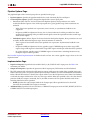
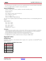
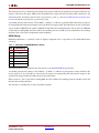
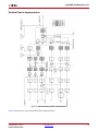
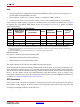
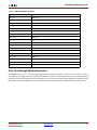
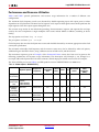
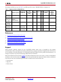
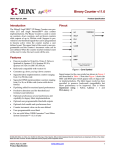
LogiCORE IP DSP48 Macro v2.1 DS754 March 1, 2011 Product Specification Introduction LogiCORE IP Facts Table The Xilinx LogiCORE™ DSP48 Macro provides an easy-to-use interface that abstracts the XtremeDSP™ slice and simplifies its dynamic operation by enabling the specification of multiple operations via a set of userdefined arithmetic expressions. The specified operations are enumerated and can be selected by the user via a single port on the generated core. Features Core Specifics Supported Device Family (1) Virtex-7 and Kintex-7 Virtex-6, Virtex-5, Virtex-4, Spartan-6, Spartan-3/XA, Spartan-3E/XA, Spartan-3A/3AN/3ADSP/XA Supported User Interfaces Not Applicable Resources (2) Configuration LUTs FFs DSP Slices Block RAMs Max. Freq. Accumulator 50 102 1 0 472 MHz Virtex®-7 Drop-in module for and Kintex™-7, Virtex-6, Virtex-5, Virtex-4, Spartan®-6/XA, Spartan-3/XA, Spartan-3E/XA, Spartan-3A/3AN/3A DSP/XA FPGAs Frequency Provided with Core Documentation Product Specification Design Files Simplified and abstracted interface to XtremeDSP slice enhances ease of use, code readability and portability Define XtremeDSP slice operation via a list of userdefined arithmetic expressions Support for up to 64 instructions Supports the XtremeDSP slice pre-adder Configurable latency Choose between XtremeDSP Slice or fabric implementation Netlist Example Design Not Provided Test Bench Not Provided Constraints File Simulation Model Not Applicable VHDL behavioral model in the xilinxcorelib library VHDL UniSim structural model Verilog UniSim structural model Tested Design Tools Design Entry Tools Simulation Support of signed, two’s complement input data For use with Xilinx CORE Generator™ and Xilinx System Generator for DSP 13.1 CORE Generator tool 13.1 System Generator for DSP 13.1 Mentor Graphics ModelSim v6.6d Cadence Incisive Enterprise Simulator v10.2 Synopsys VCS and VCS MX 2010.06 ISIM13.1 Synthesis Tools N/A Support Provided by Xilinx, Inc. 1. For a complete listing of supported devices, see the release notes for this core. 2. Resources listed here are for Virtex-6 devices. For more complete device performance numbers, see Performance and Resource Utilization, page 15. © Copyright 2009-2011, Xilinx, Inc. XILINX, the Xilinx logo, ISE, Kintex, Spartan, Virtex, and other designated brands included herein are trademarks of Xilinx in the United States and other countries. MATLAB and Simulink are registered trademarks of The MathWorks, Inc. All other trademarks are the property of their respective owners. DS754 March 1, 2011 Product Specification www.xilinx.com 1 LogiCORE IP DSP48 Macro v2.1 Pinout X-Ref Target - Figure 1 #,+ 0 3#,2 #!229/54 #% $ !#/54 ! "#/54 0#/54 " #/.#!4 #!229#!3#/54 # #!229). !#). "#). 0#). #!229#!3#). 3%, #%$ #%$ #%3%, #%3%, 3#,2$ 3#,23%, Figure 1: Core Schematic Symbol Figure 1 and Table 1 illustrate and define the schematic symbol signal names. All control inputs are active high. Should an active low input be required for a specific control pin, an inverter must be placed in the path to the pin and will be absorbed appropriately during synthesis and/or mapping. Table 1: Core Signal Pinout Signal Direction Optional CLK Input No Clock – active rising edge. CE Input Yes Clock Enable – core clock enable (active High). SCLR Input Yes Synchronous Clear – synchronous reset (active High). Asserting SCLR synchronously with CLK resets all registers. SCLR has priority over CE. D [d_width-1:0] Input Yes D port – primary input to XtremeDSP slice pre-adder. Pre-adder supported only on Virtex-7, Kintex-7, Virtex-6, Spartan-6 and Spartan-3ADSP. Maximum d_width: Virtex-5/6/7, Kintex-7 – 25 bits Other families – 18 bits A [a_width-1:0] Input Yes A port – input to XtremeDSP slice multiplier and secondary input (subtrahend) to pre-adder (supported families only). Maximum a_width: Virtex-5/6/7, Kintex-7 – 25 bits Other families – 18 bits ACIN [ac_width:0] Input Yes Cascaded A port – used as per the A port but must be driven by the ACOUT of the previous XtremeDSP slice, avoids fabric routing and logic. Static selection between A and ACIN is made by the specified DSP Macro instructions. Fixed ac_width: Virtex-5/6/7, Kintex-7 – 25 bits sign extended to 30 Other families – 18 bits DS754 March 1, 2011 Product Specification Description www.xilinx.com 2 LogiCORE IP DSP48 Macro v2.1 Table 1: Core Signal Pinout (Cont’d) Signal Direction Optional B [b_width-1:0] Input Yes B port – second input to multiplier. Maximum b_width: 18 bits BCIN [bc_width-1:0] Input Yes Cascaded B port. Must be driven by the BCOUT of the previous XtremeDSP slice. Static selection between B and BCIN. Available only on Virtex-5/6/7 and Kintex-7. Fixed bc_width: 18 bits CONCAT [concat_width-1:0] Input Yes CONCAT port – concatenation of the A and B XtremeDSP slice inputs. The D input is included in the concatenation for all devices except Virtex-4/5. Input to second stage add/sub. Mutually exclusive to the A,B and D ports. Maximum concat_width: Virtex-4 – 36 bits Other families – 48 bits Note: The A port, when specified, can be passed directly to the add/sub. C [c_wdth-1:0] Input Yes C port – input to XtremeDSP slice add/sub. Maximum c_width: 48 bits PCIN [pc_width-1:0] Input Yes PCIN port – cascaded P input from the previous XtremeDSP slice. Input to add/sub. Avoids fabric routing and provides a low latency path. Fixed pc_width: 48 bits CARRYIN Input Yes CARRYIN port – carry input from fabric, single bit. CARRYCASCIN Input Yes CARRYCASCIN port - cascaded carry input from the previous XtremeDSP slice. Can be used to construct large adders. SEL [sel_width-1:0] Input Yes SEL port - selects from the enumerated list of instructions specified in the core GUI. Unsigned. Fixed sel_width: ceil(log2(num_instructions)) CED1..3 Input Yes Clock enables for D path registers (active High) (1) CEA1..4 Input Yes Clock enables for A path registers (active High)(1) CEB1..4 Input Yes Clock enables for B path registers (active High)(1) CECONCAT3..5 Input Yes Clock enables for CONCAT path registers (active High)(1) CEC1..5 Input Yes Clock enables for C path registers (active High)(1) CEM Input Yes Clock enables for M path registers (active High)(1) CEP Input Yes Clock enables for P path registers (active High)(1) CESEL1..5 Input Yes Clock enables for SEL path registers (active High)(1) SCLRD Input Yes Synchronous reset for D path registers (active High) SCLRA Input Yes Synchronous reset for A path registers (active High) SCLRB Input Yes Synchronous reset for B path registers (active High) SCLRCONCAT Input Yes Synchronous reset for CONCAT path registers (active High) SCLRC Input Yes Synchronous reset for C path registers (active High) SCLRM Input Yes Synchronous reset for M path registers (active High) SCLRP Input Yes Synchronous reset for P path registers (active High) SCLRSEL Input Yes Synchronous reset for SEL path registers (active High) DS754 March 1, 2011 Product Specification Description www.xilinx.com 3 LogiCORE IP DSP48 Macro v2.1 Table 1: Core Signal Pinout (Cont’d) Signal P [p_msb-p_lsb:0] Direction Optional Output No Description P port - output from XtremeDSP slice add/sub, provides the selected instruction’s result. Maximum p_msb: 47 bits Note: p_msb and p_lsb are derived from the Output Port Properties; Full Precision Width and Width. See CORE Generator Graphical User Interface for more details. CARRYOUT Output Yes CARRYOUT port - carryout to fabric from add/sub. ACOUT [ac_width-1:0] Output Yes ACOUT port - optional cascade A output, ac_width defined for ACIN. BCOUT [bc_width-1:0] Output Yes BCOUT port - optional cascade B output, bc_width defined for BCIN. PCOUT [pc_width-1:0] Output Yes PCOUT port - optional cascade P output, pc_width defined for PCIN. CARRYCASCOUT Output Yes CARRYCASCOUT port - optional cascade carryout output. 1. For Virtex and Kintex devices, separate clock enable pins are available for each register stage on a path. For Spartan-6 and Spartan-3ADSP devices, the clock enables are ganged on a per-path basis. CORE Generator Graphical User Interface The DSP48 Macro core GUI has three pages used to configure the core plus two informational tabs. Tab 1: IP Symbol The IP Symbol tab illustrates the core pinout. Tab 2: Instruction Summary The Instruction Summary tab displays the complete list of specified instructions and the SEL value that is required to select each instruction. Instructions Page This page is used to specify the instructions that the core is to implement. • Component Name: The name of the core component to be instantiated. The name must begin with a letter and be composed of the following characters: a to z, 0 to 9, and “_”. • Available instructions: Informational parameter. The parameter displays all the available instructions that the core supports given the CORE Generator project family. When the “Show Filtered” check-box is ticked, the available instruction list dynamically updates to show the remaining valid instructions given the instruction that is currently being entered into the GUI. Instructions can be selected in the Available instruction panel and “drag and dropped” into an Instruction parameter. • Instructions 0 to 7: Specifies the operations the core is to implement. Text entry of the desired arithmetic operation to be generated on the P output port. The left side of the expression, P=, is implicitly declared and should not be specified. Instructions are case insensitive. Valid operands: D, A, ACIN, B, BCIN, CONCAT, C, PCIN, CARRYIN, CARRYCASCIN, 0 Valid operators: +, -, *, >>17, (, ) Valid functions: rndsimple, rndsym Example instructions: A*B+C, (D+A)*B+PCIN, P-CONCAT-C, rndsym(PCIN) See Instruction Format for further details on the instruction format and supported operations. • Instructions 8 to 63: Specifies instructions 8 to 63 using a comma-delimited list of instructions. DS754 March 1, 2011 Product Specification www.xilinx.com 4 LogiCORE IP DSP48 Macro v2.1 Pipeline Options Page The pipeline depths of the various input paths are specified on this page. • Pipeline Options: Specifies the pipeline method to be used: Automatic, By Tier and Expert. • Custom Pipeline options: Specifies the pipeline depth of the various input paths. • • Tier 1 to 6: When “By Tier” has been selected for Pipeline Options, these parameters are used to enable/disable the registers across all the input paths for a given pipeline stage. Some restrictions are enforced. - When P has been specified in an expression, tier 6 is forced, as asynchronous feedback is not supported. - In Spartan-3ADSP and Spartan-6 devices, tier 3 is forced when tier 5 and the pre-adder have been specified. The registering of the pre-adder control signals cannot be separated from the second stage adder control signals. Individual registers: When “Expert” has been selected for the Pipeline Options, these parameters are used to enable/disable individual register stages. Some restrictions are enforced. - The P register is forced when P has been specified in an expression. Asynchronous feedback is not supported. - In Spartan-3ADSP and Spartan-6 devices, pipeline stage 5 CARRYIN register is tied to stage 5 SEL register. Stage 3 SEL register is forced when stage 5 SEL register and the pre-adder have been specified. - In a Virtex-4 device, pipeline stage 5 CARRYIN register is forced when a rounding function on any multiplier input has been specified. See Detailed Pipeline Implementation for further details on how the various pipeline stages relate to the core implementation. Implementation Page • Input Port Properties: Specifies the bit-width of the D, A, B, CONCAT and C input ports. See Table 1 for maximum port widths. • Output Port Properties: Specifies the precision of the P output port; Full Precision and User Defined. • The GUI automatically calculates the full precision output width given the width of the specified input ports. When P has been used as an operand, the full precision output width is set to the full XtremeDSP slice width of 48 bits. When Full Precision is selected, the output width is set to the full precision value. When User Defined is selected, the output width can be set to any value up to 48 bits. When the specified value is less than the full precision width, the output is truncated, that is, the LSBs are removed. This option should be used when a rounding function has been specified. • • Width: Specifies the actual output width of the P output port. When specified to be less than Full Precision, the XtremeDSP slice output is truncated. Additional Ports: Specifies if the core will have a CARRYOUT output port or the ACOUT, BCOUT, PCOUT or CARRYCASCOUT cascaded output ports. DS754 March 1, 2011 Product Specification www.xilinx.com 5 LogiCORE IP DSP48 Macro v2.1 • Control Ports: • • • CE - Global checkbox: enables a single CE pin for all registers in the core. - D, A, B, CONCAT, C, M, P, SEL/CARRYIN checkboxes: enable individual CE pins for all enabled registers in the core. For Virtex and Kintex devices, a CE pin for each register will be enabled. For Spartan-6 and Spartan-3ADSP devices, a single CE pin for each datapath will be enabled. SCLR - Global checkbox: enables a single SCLR pin for all registers in the core. - D, A, B, CONCAT, C, M, P, SEL/CARRYIN checkboxes: enable an individual SCLR pin for each datapath. Use XtremeDSP Slice: Specifies if the core implementation uses an XtremeDSP slice or fabric equivalent. When a fabric implementation is specified, the core is unlikely to achieve the same Fmax as an XtremeDSP slice. Using the DSP48 Macro IP Core The CORE Generator GUI performs error-checking on all input parameters. Several files are produced when a core is generated, and customized instantiation templates for Verilog and VHDL design flows are provided in the .veo and .vho files, respectively. For detailed instructions, see the CORE Generator software documentation. Instruction Format The instructions are case insensitive and ignore spaces between operands. The left side of the arithmetic expression, P=, is implicitly declared and should not be specified Valid operands: D, A, ACIN, B, BCIN, CONCAT, C, PCIN, CARRYIN, CARRYCASCIN, 0. Valid operators: +, -, *, >>17, (, ). - The >>17 operator targets the XtremeDSP slice 17-bit wire shift; this is available only on Virtex and Kintex families. Valid only for P and PCIN operators. Valid functions: rndsimple, rndsym - Rounding functions require that the P output width is less than full precision. - See Supported Functions for further details. Examples Accumulator 1. C : Load 2. C+P : Accumulate (add) 3. P-C : Accumulate (subtract) Three input add: 1. C+CONCAT+P Multiply Accumulate 1. A*B : Load 2. P+A*B: Multiply accumulate 15-tap symmetric filter, where data is provided sequentially on the A,D and B inputs. A and D are used for the data values and B is used for the filter coefficients. DS754 March 1, 2011 Product Specification www.xilinx.com 6 LogiCORE IP DSP48 Macro v2.1 1. (A+D)*B : Taps 1 & 15 2. (A+D)*B+P : Taps 2...7 & 14...9 3. A*B+P : Tap 8 4. rndsym(P) : Round result Construction of Supported instructions The following two sections illustrate how the list of supported instructions are constructed for the main FPGA device variants: Virtex, Kintex, and Spartan. Notation varname = [ l1,l2,....] The above indicates varname supports the list of operator/operand combinations l1, l2, .... Virtex-4/-5/-6/-7 and Kintex-7 preadder = [ (A+D) , (D+A) , (D-A), D, -A , A, (ACIN+D) , (D+ACIN) , (D-ACIN), -ACIN , ACIN ] Pre-adder supported only on Virtex-6/-7 and Kintex-7. mult_ip1 = [ ACIN , A , preadder ] mult_ip2 = [ BCIN , B , 1 ] mult = [ mult_ip1 * mult_ip2 , mult_ip2 * mult_ip1 ] The 1 is not explicitly required when defining an instruction; the 1 and corresponding * operator are ignored. ACIN is not supported for Virtex-4. xmux = [ CONCAT , P , 0 ] ymux = [ C , 0 ] zmux = [ C , PCIN , P , P>>17 , PCIN>>17, 0 ] cinmux = [ CARRYIN , CARRYCASCIN , 0 ] Similarly, 0 is not explicitly required when defining an instruction. The 0 and corresponding operator are ignored. CARRYCASCIN is not supported on Virtex-4. xycomb = [ xmux + ymux , ymux + xmux , mult ] valid instructions = [ xycomb + zmux + cinmux , zmux + xycomb + cinmux , zmuz - ( xycomb + cinmux ) , zmux - xmux - ymux - cinmux , zmux - ymux - xmux - cinmux , rndsimple( zmux + xmux + cinmux ) rndsym( [ P , PCIN ] ) ] Note that for the rndsimple functions, operand C is not supported for zmux. Restrictions • CONCAT operand is mutually exclusive to mult operands. When any input to the multiplier is specified, the CONCAT operand is restricted for all instructions, or vice versa. The inclusion of 1 in mult_ip2 enables all mult_ip1 combinations to be used as direct inputs to the second stage add/sub. DS754 March 1, 2011 Product Specification www.xilinx.com 7 LogiCORE IP DSP48 Macro v2.1 • The choice between A and ACIN is static; once one is specified the other is restricted. Similarly for B and BCIN. • The use of CARRYCASCIN is restricted to a subset of instructions. Spartan-3ADSP/Spartan-6 preadder = [ (A+D) , (D+A) , (D-A), A, (ACIN+D) , (D+ACIN) , (D-ACIN), ACIN ] mult_ip1 = [ preadder ] mult_ip2 = [ B , 1 ] mult = [ mult_ip1 * mult_ip2 , mult_ip2 * mult_ip1 ] xmux = [ CONCAT , P , mult , 0 ] zmux = [ C , PCIN , P , 0 ] cinmux = [ CARRYIN , CARRYCASCIN , 0 ] The 0 and 1 are not explicitly required when defining an instruction. The 0, or 1, and corresponding operator are ignored. valid instructions = [ zmux + xmux + cinmux , xmux + zmuz + cinmux , zmux - ( xmux + cinmux ) , zmux - xmux - cinmux , rndsimple( xmux + cinmux ) ] Restrictions • CONCAT operand is mutually exclusive to mult operands. When any input to the multiplier is specified, the CONCAT operand is restricted for all instructions, or vice versa. The inclusion of 1 in mult_ip2 enables all mult_ip1 combinations to be used as direct inputs to the second stage add/sub. • The choice between A and ACIN is static; once one is specified the other is restricted. • If CARRYCASCIN is specified, all further instructions will require CARRYCASCIN. Supported Functions RNDSIMPLE(arg) RNDSIMPLE implements a non-symmetric round to negative; this is equivalent to the MATLAB® software function ceil(arg-0.5). Table 2: Illustration of RNDSIMPLE Return Values arg RNDSIMPLE(arg) <x.5 x x.5 x >x.5 x+1 >-x.5 -x -x.5 -x-1 <-x.5 -x-1 DS754 March 1, 2011 Product Specification www.xilinx.com 8 LogiCORE IP DSP48 Macro v2.1 The binary point of arg is defined by the full precision output width and the specified core output width; the core output is taken from the upper MSBs of the XtremeDSP slice output with the remaining LSBs considered as the fractional portion. The binary point is taken as full precision p_width - p_width. See CORE Generator Graphical User Interface for details on full precision p_width and p_width. A rounding constant with a binary value of 0.0111...(or 0.499...) is added to arg and the LSBs removed by the process of reinterpreting the full precision output to the specified core output width. The LSBs remain on the accumulator. Arg can include CARRYIN. This enables CARRYIN to determine the rounding direction. The assertion of CARRYIN is equivalent to adding 0.00...01. This modifies the rounding constant to 0.100.. (or 0.5) and therefore the rounding direction. This can be used to implement random rounding. RNDSYM(arg) RNDSYM implements a symmetric round to highest magnitude; this is equivalent to the MATLAB function round(arg). Table 3: Illustration of RNDSYM Return Values arg RNDSYM(arg) <x.5 x x.5 x+1 >x.5 x+1 >-x.5 -x -x.5 -x-1 <-x.5 -x-1 The binary point of arg is defined in the same manner as for the RNDSIMPLE(arg) function. A rounding constant with a binary value of 0.0111.... (or 0.499...) is added to arg along with a carryin, defined as the inverse sign bit of arg. The LSBs are removed by the process of reinterpreting the full precision output to the specified core output width. The LSBs remain on the accumulator. When carryin is 1, this is equivalent to adding 0.00....01. This modifies the rounding constant to 0.100.. (or 0.5) and therefore the rounding direction. This function is available only on Virtex and Kintex families. DS754 March 1, 2011 Product Specification www.xilinx.com 9 LogiCORE IP DSP48 Macro v2.1 Detailed Pipeline Implementation X-Ref Target - Figure 2 Figure 2: DSP48 Macro Detailed Implementation Figure 2 illustrates the generalized DSP48 Macro implementation. DS754 March 1, 2011 Product Specification www.xilinx.com 10 LogiCORE IP DSP48 Macro v2.1 Note: • The second stage add/sub input mux implementations vary depending on the selected device. • Generally register CC4 is implemented using only XtremeDSP slice resources, but for some target devices it uses both fabric and XtremeDSP slice resources. • The pre-adder is available only on Virtex-6/-7, Kintex-7, and Spartan-3ADSP/-6 FPGAs. • A static mux is resolved at core generation, whereas a dynamic mux is implemented in the generated core. Users requiring a specific mapping to registers in the DSP48 primitive of a particular device family can use Table 4 to determine the corresponding DSP48 Macro registers. See References for a list of user guides with DSP48 primitive information. Table 4: Register Mapping for DSP48 Macro DSP48 Macro Virtex-6/Virtex-7/ Kintex-7 (using pre-adder)[1] D3 D N/A N/A A3 A1 A1 A4 AD B3 B4 Virtex-6/Virtex-7/Kintex-7 Spartan-6 / Virtex-5 Spartan-3ADSP (no pre-adder) Virtex-4[2] Spartan-3 Variants[3] D N/A N/A A1 B0 A (stage 1) CLB logic A2 A2 B1 A (stage 2) CLB logic B1 B1 B1 A0 B (stage 1) CLB logic B2 B2 B2 A1 B (stage 2) CLB logic [1] The mapping of A4 changes on Virtex-6/Virtex-7/Kintex-7 depending on whether the pre-adder is used so the tiered latency model is maintained. [2] Virtex-4 2-deep A and B registers cannot be separately controlled. If separate clock enables are specified in the GUI, the stage 1 registers will be implemented in CLB logic. [3] Spartan-3/A/E FPGA devices do not have an XtremeDSP slice. Input registers are implemented in CLB logic. Simulation Models The core has a number of options for simulation models: • VHDL behavioral model in the xilinxcorelib library • VHDL UniSim-based structural simulation model • Verilog UniSim-based structural simulation model The models required may be selected in the CORE Generator project options. Xilinx recommends that simulations utilizing UniSim-based structural models are run using a resolution of 1 ps. Some Xilinx library components require a 1 ps resolution to work properly in either functional or timing simulation. The UniSim-based structural simulation models may produce incorrect results if simulated with a resolution other than 1 ps. See the “Register Transfer Level (RTL) Simulation Using Xilinx Libraries” section in Chapter 6 of the Synthesis and Simulation Design Guide for more information. This document is part of the ISE® Software Manuals set available at ww.xilinx.com/support/software_manuals.htm. XCO Parameters Table 5 defines valid entries for the XCO parameters. Parameters are not case sensitive. Default values are displayed in bold. Xilinx strongly suggests that XCO parameters are not manually edited in the XCO file; instead, use the CORE Generator GUI to configure the core and perform range and parameter value checking. The XCO parameters are helpful in defining the interface to other Xilinx tools. DS754 March 1, 2011 Product Specification www.xilinx.com 11 LogiCORE IP DSP48 Macro v2.1 Table 5: XCO Parameters XCO Parameter Valid Values component_name ASCII text using characters: a..z, 0..9 and ‘_’ ; starting with a letter instruction1 ASCII text; see Instructions Page and Instruction Format for details on valid instruction format. Default: A*B+C instruction2 ASCII text instruction3 ASCII text instruction4 ASCII text instruction5 ASCII text instruction6 ASCII text instruction7 ASCII text instruction8 ASCII text instruction_list ASCII text, comma delimited list of instructions 8 to 64. pipeline_options Automatic, By_Tier, Expert tier_1 ... _6 false, true dreg_1 ... _3 false, true areg_1 ... _4 false, true breg_1 ... _4 false, true creg_1 ... _5 false, true concatreg_3 ... _5 false, true opreg_1 ... _5 false, true cinreg_1 ... _5 false, true mreg_5 false, true preg_6 true, false d_width 2 - 18, Default is 18 a_width 2 - 18/25, Default is 18 b_width 2 - 18, Default is 18 concat_width 2 - 36/48, Default is 36/48 (depends on target FPGA device) c_width 2 - 48, Default is 48 output_properties Full_Precision, User_Defined p_width 2 - 48, Default is set to p_full_width p_full_width 2 - 48, Default is 48 has_carryout false, true has_acout false, true has_bcout false, true has_carrycascout false, true has_pcout false, true DS754 March 1, 2011 Product Specification www.xilinx.com 12 LogiCORE IP DSP48 Macro v2.1 Table 5: XCO Parameters (Cont’d) has_ce false, true has_d_ce false, true has_a_ce false, true has_b_ce false, true has_c_ce false, true has_concat_ce false, true has_m_ce false, true has_p_ce false, true has_sel_ce false, true has_sclr false, true has_d_sclr false, true has_a_sclr false, true has_b_sclr false, true has_c_sclr false, true has_concat_sclr false, true has_m_sclr false, true has_p_sclr false, true has_sel_sclr false, true use_dsp48 true, false Core Use through System Generator The DSP48 Macro core is available through Xilinx System Generator for DSP, a design tool that enables the use of the model-based design environment Simulink® for FPGA design. The DSP48 Macro core is one of the DSP building blocks provided in the Xilinx blockset for Simulink. The core can be found in the Xilinx Blockset in the DSP section. The block is called “DSP48 Macro v2.1.” See the System Generator for DSP User Manual for more information. DS754 March 1, 2011 Product Specification www.xilinx.com 13 LogiCORE IP DSP48 Macro v2.1 System Generator for DSP Graphical User Interface This section describes each tab of the System Generator for DSP GUI and details the parameters that differ from the CORE Generator GUI. Tab 1: Instructions The Instruction tab is used to define the operations that the core is to implement. Each instruction can be entered on a new line, or in a comma delimited list, and are enumerated from the top down. A maximum of 64 instructions can be specified. See Instructions Page of CORE Generator Graphical User Interface and Instruction Format of Using the DSP48 Macro IP Core for details on supported instructions and their format. Tab 2: Pipeline Options The Pipeline Options tab is used to define the pipeline depth of the various input paths. Refer to the Pipeline Options Page of CORE Generator Graphical User Interface for details of all the core parameters on this tab. Tab 3: Implementation The Implementation tab is used to define implementation options. Refer to the Implementation Page of CORE Generator Graphical User Interface for details of all the core parameters on this tab. • Output Port Properties: Specifies the precision of the P output port; Full Precision and User Defined. • The core automatically calculates the full precision output width and binary point position given the width and binary point of the specified input ports. When P has been used as an operand, the full precision output width is set to the full XtremeDSP slice width of 48 bits. • When Full Precision is selected, the output is set to full precision width and binary point. • When User Defined is selected, the output width can be set to any value up to 48 bits. The output formatting has two modes of operation: Full precision binary point is calculated to be zero. - When the output width is specified to be less than the full precision width, the output will be truncated, that is, the LSBs will be removed. Full precision binary point is calculated to be greater than zero. - The binary point is anchored. The output of the core behaves in the same manner as a System Generator Convert block with the following settings: Quantization -> Truncate and Overflow -> Wrap. Some restrictions on the binary point values will be enforced; it cannot be greater than the full precision binary point value and its permitted minimum value will be modified to ensure that when the binary point value and output width are combined, the resulting MSB value does not exceed 48 bits. • Width: Specifies the user-defined output width of the P output port. • Binary Point: Specifies the user-defined binary point of the P output port. • ce: Selects either a global clock enable pin, or separate clock enable pins for each register (Virtex/Kintex devices) or datapath (Spartan devices). When separate clock enable pins are selected, these are managed within System Generator to correctly handle multi-rate constraints. • rst: Selects either a global reset pin, or separate reset pins for each datapath. In a similar way to the separate clock enable pins, System Generator manages the situation where datapaths with separate reset controls have different rates. • FPGA Area Estimation: See the System Generator for DSP documentation for detailed information about this section. DS754 March 1, 2011 Product Specification www.xilinx.com 14 LogiCORE IP DSP48 Macro v2.1 Performance and Resource Utilization Table 6 and Table 7 provide performance and resource usage information for a number of different core configurations. The maximum clock frequency results were obtained by double-registering input and output ports to reduce dependence on I/O placement. The inner level of registers used a separate clock signal to measure the path from the input registers to the first output register through the core. The resource usage results do not include the preceding “characterization” registers and represent the true logic used by the core to implement a single multiplier. LUT counts include SRL16s or SRL32s (according to device family). The map options used were: “map -ol high“ The par options used were: “par -ol high” Clock frequency does not take clock jitter into account and should be derated by an amount appropriate to the clock source jitter specification. The maximum achievable clock frequency and the resource counts may also be affected by other tool options, additional logic in the FPGA device, using a different version of Xilinx tools, and other factors. The instruction sequences given in Examples of the Instruction Format section have been used to generate the following performance and resource usage information. The three-input add, Example 2, was changed to a two-input add for the Spartan FPGA resource estimates. Default input port widths were used for all examples. The Virtex-6 FPGA test cases in Table 6 used ISE speed file version "PRODUCTION 1.13a 2010-12-13." Table 6: Virtex-6 (Part = XC6VLX75T-1) Pipeline Options Example 1 Automatic (Accumulator) Maximum Clock Frequency (MHz) Output Port Properties Use XtremeDSP Slice Full Precision Yes 52 50 102 1 472 LUT/FF LUT6s FFs XtremeDSP Pairs Slices Example 2 (Three-input add) Expert (PREG6, CREG5, CONCATREG3, CONCATREG4) Full Precision Yes 0 0 0 1 472 Example 3 (Multiply Accumulate) Automatic Full Precision Yes 2 2 4 1 472 Example 4 (FIR Filter) Automatic User Defined 18-bit output Yes 6 2 8 1 472 Example 5 (FIR Filter) Automatic User Defined 18-bit output No 784 741 239 0 147 DS754 March 1, 2011 Product Specification www.xilinx.com 15 LogiCORE IP DSP48 Macro v2.1 The Spartan-6 FPGA test cases in Table 7 used ISE speed file version "PRODUCTION 1.15 2010-12-13." Table 7: Spartan-6 (Part = XC6SLX75-2) Maximum Clock Frequency (MHz) Output Port Properties Use XtremeDSP Slice Full Precision Yes 53 50 102 1 298 Expert (PREG6, CREG5, CONCATREG5) Full Precision Yes 0 0 0 1 319 Example 3 (Multiply Accumulate) Automatic Full Precision Yes 2 2 4 1 298 Example 4 (FIR Filter) Automatic User Defined 18-bit output Yes 5 2 6 1 298 Example 5 (FIR Filter) Automatic User Defined 18-bit output No 668 627 289 0 81 Pipeline Options Example 1 Automatic (Accumulator) Example 2 (Two-input add) LUT/FF LUT6s FFs XtremeDSP Pairs Slices References 1. XtremeDSP for Virtex-4 FPGAs User Guide 2. Virtex-5 FPGA XtremeDSP Design Considerations User Guide 3. Virtex-6 FPGA DSP48E1 Slice User Guide 4. XtremeDSP DSP48A for Spartan-3A DSP FPGAs User Guide 5. Spartan-6 FPGA DSP48A1 Slice User Guide 6. 7 Series FPGA DSP48E1 Slice User Guide Support Xilinx provides technical support for this LogiCORE product when used as described in the product documentation. Xilinx cannot guarantee timing, functionality, or support of product if implemented in devices that are not defined in the documentation, if customized beyond that allowed in the product documentation, or if changes are made to any section of the design labeled DO NOT MODIFY. Refer to the IP Release Notes Guide (XTP025) for further information on this core. There is a link to all the DSP IP and then to each core. For each core, there is a master Answer Record that contains the Release Notes and Known Issues list for each core. The following information is listed for each version of the core: • New Features • Bug Fixes • Known Issues DS754 March 1, 2011 Product Specification www.xilinx.com 16 LogiCORE IP DSP48 Macro v2.1 Ordering Information This LogiCORE IP module is included at no additional cost with the Xilinx ISE Design Suite software and is provided under the terms of the Xilinx End User License Agreement. Use the CORE Generator software included with the ISE Design Suite to generate the core. For more information, please visit the core page. Please contact your local Xilinx sales representative for pricing and availability of additional Xilinx LogiCORE modules and software. Information about additional Xilinx LogiCORE modules is available on the Xilinx IP Center. Revision History The following table shows the revision history for this document: Date Version Description of Revisions 12/02/09 1.0 Initial Xilinx release. 03/01/11 2.0 Support added for Virtex-7, Kintex-7, and ISE Design Suite 13.1. Added details of separate CE and SCLR controls. Notice of Disclaimer Xilinx is providing this product documentation, hereinafter “Information,” to you “AS IS” with no warranty of any kind, express or implied. Xilinx makes no representation that the Information, or any particular implementation thereof, is free from any claims of infringement. You are responsible for obtaining any rights you may require for any implementation based on the Information. All specifications are subject to change without notice. XILINX EXPRESSLY DISCLAIMS ANY WARRANTY WHATSOEVER WITH RESPECT TO THE ADEQUACY OF THE INFORMATION OR ANY IMPLEMENTATION BASED THEREON, INCLUDING BUT NOT LIMITED TO ANY WARRANTIES OR REPRESENTATIONS THAT THIS IMPLEMENTATION IS FREE FROM CLAIMS OF INFRINGEMENT AND ANY IMPLIED WARRANTIES OF MERCHANTABILITY OR FITNESS FOR A PARTICULAR PURPOSE. Except as stated herein, none of the Information may be copied, reproduced, distributed, republished, downloaded, displayed, posted, or transmitted in any form or by any means including, but not limited to, electronic, mechanical, photocopying, recording, or otherwise, without the prior written consent of Xilinx. DS754 March 1, 2011 Product Specification www.xilinx.com 17