1
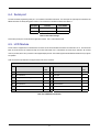
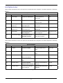
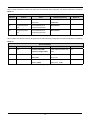
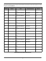
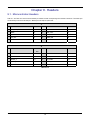
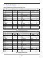
REJ10J1303-0200
Renesas Starter Kit for R8C/1B
User’s Manual
RENESAS 16-BIT SINGLE-CHIP MICROCOMPUTER
M16C FAMILY / R8C/Tiny SERIES
Rev.2.00
Revision date: Aug.31,.2007
Renesas Solutions Corp.
www.renesas.com
i
Table of Contents
Chapter 1. Preface .................................................................................................................................................. 1
Chapter 2. Purpose ................................................................................................................................................. 2
Chapter 3. Power Supply ........................................................................................................................................ 3
3.1. Requirements ............................................................................................................................................... 3
3.2. Power – Up Behaviour ................................................................................................................................. 3
Chapter 4. Board Layout ......................................................................................................................................... 4
4.1. Component Layout ....................................................................................................................................... 4
4.2. Board Dimensions ........................................................................................................................................ 5
Chapter 5. Block Diagram ....................................................................................................................................... 6
Chapter 6. User Circuitry......................................................................................................................................... 7
6.1. Switches ....................................................................................................................................................... 7
6.2. LEDs ............................................................................................................................................................. 7
6.3. Potentiometer ............................................................................................................................................... 7
6.4. Serial port ..................................................................................................................................................... 8
6.5. LCD Module.................................................................................................................................................. 8
6.6. Option Links.................................................................................................................................................. 9
6.7. Oscillator Sources ...................................................................................................................................... 12
6.8. Reset Circuit ............................................................................................................................................... 12
Chapter 7. Modes.................................................................................................................................................. 13
7.1. Boot mode .................................................................................................................................................. 13
7.2. Single chip mode ........................................................................................................................................ 13
Chapter 8. Programming Methods........................................................................................................................ 14
Chapter 9. Headers............................................................................................................................................... 15
9.1. Microcontroller Headers ............................................................................................................................. 15
9.2. Application Headers ................................................................................................................................... 16
Chapter 10. Code Development ........................................................................................................................... 17
10.1. Overview................................................................................................................................................... 17
10.2. Mode Support ........................................................................................................................................... 17
10.3. Breakpoint Support................................................................................................................................... 17
10.4. Memory Map............................................................................................................................................. 18
Chapter 11. Component Placement...................................................................................................................... 19
Chapter 12. Additional Information ....................................................................................................................... 20
ii
Chapter 1. Preface
Cautions
This document may be, wholly or partially, subject to change without notice.
All rights reserved. Duplication of this document, either in whole or part is prohibited without the written permission of Renesas
Solutions Corp.
Trademarks
All brand or product names used in this manual are trademarks or registered trademarks of their respective companies or
organisations.
Copyright
© Renesas Solutions Corp. 2007. All rights reserved.
© Renesas Technology Europe Ltd. 2007. All rights reserved.
© Renesas Technology Corp. 2007. All rights reserved.
Website:
http://www.eu.renesas.com/
(Europe)
http://www.america.renesas.com/
(America)
Glossary
ADC
Analog Digital Converter
IRQ
Interrupt ReQuest
CPU
Central Processing Unit
LCD
Liquid Crystal Display
DAC
Digital Analog Converter
LED
Light Emitting Diode
E8a
E8a On-chip debugger module
LSI
Large Scale Integration
HEW
High-performance Embedded Workshop
MCU
Microcontroller
1
Chapter 2. Purpose
This Renesas Starter Kit is an evaluation tool for Renesas microcontrollers.
Features include:
•
Renesas Microcontroller Programming.
•
User Code Debugging.
•
User Circuitry such as Switches, LEDs and potentiometer(s).
•
User or Example Application.
•
Sample peripheral device initialisation code.
The Renesas Starter Kit board contains all the circuitry required for microcontroller operation.
NOTE: This manual describes the technical details of the Renesas Starter Kit for R8C/1B hardware. The Quick Start Guide and
Tutorial Manual provide details of the software installation and debugging environment.
2
Chapter 3. Power Supply
3.1. Requirements
This Renesas Starter Kit operates from a 3V to 5V power supply.
A diode provides reverse polarity protection only if a current limiting power supply is used.
All Renesas Starter Kit boards are supplied with an E8a debugger. This product is able to power the Renesas Starter Kit board with up to
300mA. When the Renesas Starter Kit is connected to another system then that system should supply power to the Renesas Starter Kit.
All Renesas Starter Kit boards have an optional centre positive supply connector using a 2.1mm barrel power jack.
Warning
The Renesas Starter Kit is neither under nor over voltage protected. Use a centre positive supply for this board.
3.2. Power – Up Behaviour
When the Renesas Starter Kit is purchased the Renesas Starter Kit board has the ‘Release’ or stand alone code from the example tutorial
code pre-programmed into the Renesas microcontroller. On powering up the board the user LEDs will start to flash. After 200 flashes, or
after pressing a switch the LEDs will flash at a rate controlled by the potentiometer.
3
Chapter 4. Board Layout
4.1. Component Layout
The following diagram shows the top layer component layout of the board.
Figure 4-1: Board Layout
4
4.2. Board Dimensions
The following diagram gives the board dimensions and connector positions. All through hole connectors are on a common 0.1” grid for easy
interfacing.
Figure 4-2 : Board Dimensions
5
Chapter 5. Block Diagram
Figure 5-1 is representative of the CPU board components and their connectivity.
Figure 5-1: Block Diagram
Figure 5-2 is representative of the connections required to the Renesas Starter Kit.
Figure 5-2 : Renesas Starter Kit Connections
6
Chapter 6. User Circuitry
6.1. Switches
There are four switches located on the Renesas Starter Kit. The function of each switch and its connection are shown in Table 6-1.
Switch
Function
Microcontroller
RES
When pressed, the Renesas Starter Kit microcontroller is reset.
RESSET Pin3
SW1/BOOT*
Connects to an IRQ input for user controls.
INT0 Pin9
The switch is also used in conjunction with the RES switch to place
(Port 4, pin 5)
the device in BOOT mode when not using the E8a debugger.
SW2*
Connects to an IRQ Interrupt input line for user controls.
INT3 Pin19
(Port 3, pin 3)
SW3*
Connects to a Key In Interrupt input line for user controls
KI1 Pin17
(Port 1, pin 1)
Table 6-1: Switch Functions
*Refer to schematic for detailed connectivity information.
6.2. LEDs
There are six LEDs on the Renesas Starter Kit board. The green ‘POWER’ LED lights when the board is powered. The orange ‘BOOT’ LED
indicates the device is in BOOT mode when lit. The four user LEDs are connected to an IO port and will light when their corresponding port
pin is set low.
Table 6-2, below, shows the LED pin references and their corresponding microcontroller port pin connections.
LED Reference
Colour
Microcontroller Port Pin function
Microcontroller Pin
(As shown on silkscreen)
Number
LED0
Green
Port 1.4
13
LED1
Orange
Port 1.5
12
LED2
Red
Port 1.6
11
LED3
Red
Port 1.7
10
Table 6-2: LED Port
6.3. Potentiometer
A single turn potentiometer is connected to AN8 (P1.0) of the microcontroller. This may be used to vary the input analog voltage value to
this pin between VREF and Ground.
7
6.4. Serial port
The microcontroller programming serial port 1 is connected to the RS232 transceiver. This serial port can optionally be connected to the
RS232 transceiver as well by fitting option resistors. The connections to be fitted are listed in the table 6-3.
Description
Function
Fit for RS232
TxD1
Programming Serial Port
R62
RxD1
Programming Serial Port
R63
Table 6-3: Serial Port settings
A Secondary serial port is connected to the application headers. This is shared with the SW1.
6.5. LCD Module
A LCD module is supplied to be connected to the connector J8. This should be fitted so that the LCD module lies over J1. Care should be
taken to ensure the pins are inserted correctly into J8.The LCD module uses a 4 bit interface to reduce the pin allocation. No contrast
control is provided; this is set by a resistor on the supplied display module. The module supplied with the Renesas Starter Kit only supports
5V operation.
Table 6-4 shows the pin allocation and signal names used on this connector.
J8
Pin
Circuit Net Name
Device
Pin
Circuit Net Name
Device
Pin
Pin
1
Ground
-
2
5V Only
-
3
No Connection
-
4
LCD_RS
20
5
R/W (Wired to Write only)
-
6
LCD_E
1
7
No Connection
-
8
No Connection
-
9
No Connection
-
10
No Connection
-
11
LCD_D4
13
12
LCD_D5
12
13
LCD_D6
11
14
LCD_D7
10
Table 6-4: LCD Module Connections
8
6.6.Option Links
Table 6-5 below describes the function of the option links associated with Power configuration. The default configuration is indicated by
BOLD text.
Option Link Settings
Reference
R8
Function
Power Supply
Fitted
Alternative (Removed)
Connects J5 to Board_VCC
J5 disconnected from
Related To
R13
Board_VCC
R10
MCU Power Supply
Supply to MCU
Fit Low ohm resistor to
R11, R12, R13
measure current
R11
R12
R13
R15
Power Supply
Connects CON_5V (external
CON_5V disconnected from
(External 5V)
5V) to Board_VCC
Board_VCC
Power Supply
Connects CON_3V3 (external
CON_3V disconnected from
(External 3.3V)
3.3V) to Board_VCC
Board_VCC
Power Supply
Connects Board_VCC to
Board_VCC disconnected from
R8, R10, R11, R12,
board voltage line
board voltage line
R14
Connects Board_VCC to
Board_VCC disconnected from
SW2, SW3 and LED0-3
SW2, SW3 and LED0-3
User I/O Power Supply
R10, R12, R13
R10, R11, R13
Table 6-5: Power Configuration Links
Table 6-6 below describes the function of the option links associated with Clock configuration. The default configuration is indicated by
BOLD text.
Option Link Settings
Reference
R1
Function
Oscillator
Fitted
Alternative (Removed)
Connects X1 to MCU
Connects external clock to
Related To
R2, R3, R4
MCU
R2
Oscillator
Connects X1 to MCU
Connects external clock to
R1, R3, R4
MCU
R3
Oscillator
Connects external clock to
Connects X1 to MCU
MCU (or use input port)
R4
Oscillator
Connects external clock to
R1, R2, R4, R54,
R55
Connects X1 to MCU
R1, R2, R3
Connects CON_XIN1
CON_XIN1 disconnected from
R3, R55
(external clock) to CON_XIN
CON_XIN
Connects CON_XIN2 (input
CON_XIN2 disconnected from
port) to CON_XIN
CON_XIN
MUC
R54
R55
Clock/Port Select
Clock/Port Select
Table 6-6: Clock Configuration Links
9
R3, R54
Table 6-7 below describes the function of the option links associated with Serial configuration. The default configuration is indicated by
BOLD text.
Option Link Settings
Reference
R30
R62
R63
Function
RS232 Serial
Fitted
Alternative (Removed)
Disables RS232 Serial
Enables RS232 Serial
Transceiver
Transceiver
Programming Serial
Connects RS232 port to
Disconnected
Port
Programming Serial Port
Programming Serial
Connects RS232 Port to
Port
Programming Serial Port
Related To
R62, R63
Disconnected
Table 6-7: Serial Configuration Links
Table 6-8 below describes the function of the option links associated with Analog configuration. The default configuration is indicated by
BOLD text.
Option Link Settings
Reference
R5
R14
R60
Function
ADC
ADC
ADC
Fitted
Alternative (Removed)
Connects CON_VREF
CON_VREF disconnected from
(reference voltage) to MCU
MCU
Connects CON_VREF to
CON_VREF disconnected from
Board_VCC
Board_VCC
Connects AD_POT to MCU
Disconnects AD_POT from
port P1_0(AN8)
MCU port P1_0(AN8)
Table 6-8: Analog Configuration Links
10
Related To
R14
R5
R38, R39
Table 6-9 below describes the function of the option links associated with microcontroller pin function select configuration. The default
configuration is indicated by BOLD text.
Option Link Settings
Reference
R38
Function
Fitted
MCU Pin Function Select
Alternative (Removed)
Connects AD0 to MCU port
Related To
Disconnected
R39, R60
Disconnected
R38, R60
Disconnected
R41
Disconnected
R40
Disconnected
R43
Disconnected
R42
Disconnected
R45
Disconnected
R44
Disconnected
R47
Disconnected
R46
Disconnected
R49
Disconnected
R48
Disconnected
R51
Disconnected
R50
Disconnected
R53
Disconnected
R52
P1_0
R39
MCU Pin Function Select
Connects IO_0 to MCU port
P1_0
R40
MCU Pin Function Select
Connects AD1 to MCU port
P1_1
R41
MCU Pin Function Select
Connects IO_1 to MCU port
P1_1
R42
MCU Pin Function Select
Connects AD2 to MCU port
P1_2
R43
MCU Pin Function Select
Connects IO_2 to MCU port
P1_2
R44
MCU Pin Function Select
Connects AD3 to MCU port
P1_3
R45
MCU Pin Function Select
Connects IO_3 to MCU port
P1_3
R46
MCU Pin Function Select
Connects SCIaRX to MCU
port P1_5
R47
MCU Pin Function Select
Connects IRQ1 to MCU port
P1_5
R48
MCU Pin Function Select
Connects TRIGb to MCU port
P3_3
R49
MCU Pin Function Select
Connects IRQ2 to MCU port
P3_3
R50
MCU Pin Function Select
Connects IIC_SDA to MCU port
P3_4
R51
MCU Pin Function Select
Connects TMR1 to MCU port
P3_4
R52
MCU Pin Function Select
Connects IIC_SCL to MCU port
P3_5
R53
MCU Pin Function Select
Connects LCD_E to MCU port
P3_5
Table 6-9: MCU Pin Function Select Configuration Links
11
Table 6-10 below describes the function of the option links associated with other options. The default configuration is indicated by BOLD
text.
Option Link Settings
Reference
Function
Fitted
Alternative (Removed)
R32
E8a
Enables E8a
Do not connect option resistor
R61
SW1
Connects SW1 to MCU port
Disconnected
Related To
P4_5
Table 6-10: Other Option Links
6.7.Oscillator Sources
A crystal oscillator is fitted on the Renesas Starter Kit and used to supply the main clock input to the Renesas microcontroller.
Table 6-11 details the oscillator that is fitted and alternative footprints provided on this Renesas Starter Kit:
Component
Crystal (X1)
Fitted
20 MHz (HC/49U package)
Table 6-11: Oscillator
6.8.Reset Circuit
The CPU Board includes a simple latch circuit that links the mode selection and reset circuit. This provides an easy method for swapping
the device between Boot Mode and Single Chip Mode. This circuit is not required on customers’ boards as it is intended for providing
easy evaluation of the operating modes of the device on the Renesas Starter Kit. Please refer to the hardware manual for more
information on the requirements of the reset circuit.
The Reset circuit operates by latching the state of the boot switch on pressing the reset button. This control is subsequently used to
modify the mode pin states as required.
The MODE pin should change state only while the reset signal is active to avoid possible device damage.
The reset is held in the active state for a fixed period by a pair of resistors and a capacitor. Please check the reset requirements carefully
to ensure the reset circuit on the user’s board meets all the reset timing requirements.
12
Chapter 7. Modes
The Renesas Starter Kit supports Boot mode and Single Chip mode.
Details of programming the FLASH memory is described in the R8C/1B Group Hardware Manual.
7.1. Boot mode
The boot mode settings for this Renesas Starter Kit are shown in Table 7-1: Boot Mode pin settings below:
MODE
LSI State after Reset End
Low
Boot Mode
Table 7-1: Boot Mode pin settings
The software supplied with this Renesas Starter Kit supports Boot mode using an E8a and High-performance Embedded Workshop only.
However, hardware exists to enter boot mode manually, do not connect the E8a in this case. Press and hold the SW1/BOOT. The MODE
pin is held in its boot state while reset is pressed and released. Release the boot button. The BOOT LED will be illuminated to indicate that
the microcontroller is in boot mode.
When neither the E8a is connected nor the board is placed in boot mode as above, the MODE pin is pulled high by a 4.7k resistor.
When an E8a is used the MODE pin is controlled by the E8a.
7.2. Single chip mode
Because the MODE pin is pulled high, this Renesas Starter Kit will always boot in Single Chip mode when the E8a is not connected and the
boot switch is not depressed. Refer to R8C/1B Group Hardware Manual for details of Single chip mode.
MODE
LSI State after Reset End
High
Single Chip Mode
Table 7-2: Single Chip Mode pin settings
13
Chapter 8. Programming Methods
The board is intended for use with High-performance Embedded Workshop and the supplied E8a debugger. Refer to R8C/1B Group
Hardware Manual for details of programming the microcontroller without using these tools.
14
Chapter 9. Headers
9.1. Microcontroller Headers
Table 9-1 and Table 9-2 show the microcontroller pin headers and their corresponding microcontroller connections. The header pins
connect directly to the microcontroller pins. * Marked pins are subject to option links.
J1
Pin
Circuit Net Name
Device Pin
Pin
Circuit Net Name
Device Pin
1
LCD_E/IIC_SCL*
1
2
TMR0
2
3
RESn
3
4
CON_XOUT
4
5
VSS
5
6
CON_XIN*
6
7
UC_VCC
7
8
MODE_E8B
8
9
IRQ0
9
10
TRIGb
10
Table 9-1: J1
J2
Pin
Circuit Net Name
Device
Pin
Circuit Net Name
Device Pin
Pin
1
SCIaCK
11
2
SCIaRX/IRQ1*
12
3
SCIaTX
13
4
AD3/IO_3*
14
5
AD2/IO_2*
15
6
P4_2/VREF
16
7
AD1/IO_1*
17
8
AD0/IO_0*
18
9
TRIGb/IRQ2*
19
10
TMR1/IIC_SDA*
20
Table 9-2: J2
15
9.2. Application Headers
Table 9-3 and Table 9-4 below show the standard application header connections.
JA1
Pin
Header Name
Circuit Net
Device
Name
Pin
Pin
Header Name
Circuit Net
Device
Name
Pin
1
Regulated Supply 1
CON_5V
-
2
Regulated Supply 1
Ground
-
3
Regulated Supply 2
CON_3V3
-
4
Regulated Supply 2
Ground
-
5
Analogue Supply
NC
-
6
Analogue Supply
NC
-
7
Analogue Reference
CON_VREF
16
8
ADTRG
NC
-
9
ADC0
AD0*
18
10
ADC1
AD1*
17
11
ADC2
AD2*
15
12
ADC3
AD3*
14
13
DAC0
NC
-
14
DAC1
NC
-
15
IOPort0
IO_0*
18
16
IOPort1
IO_1*
17
17
IOPort2
IO_2*
15
18
IOPort3
IO_3*
14
19
IOPort4
NC
-
20
IOPort5
NC
-
21
IOPort6
NC
-
22
IOPort7
NC
-
23
IRQ3
NC
-
24
I2C Bus (3rd pin)
NC
-
25
I²C Bus
IIC_SDA*
20
26
I²C Bus
IIC_SCL*
1
Table 9-3: JA1 Standard Generic Header
JA2
Pin
Header Name
Circuit Net
Device
Name
Pin
Pin
Header Name
Circuit Net
Device
Name
Pin
1
Reset
RESn
3
2
External Clock Input
CON_XIN1*
6
3
Interrupt
NC
-
4
Regulated Supply 1
Ground
-
5
SPARE
NC
-
6
Serial Port
SCIaTX
13
7
Interrupt
IRQ0
9
8
Serial Port
SCIaRX*
12
9
Interrupt
IRQ1*
12
10
Serial Port
SCIaCK
11
11
Motor up/down
NC
-
12
Serial Port Handshake
NC
-
13
Motor control
NC
-
14
Motor control
NC
-
15
Motor control
NC
-
16
Motor control
NC
-
17
Motor control
NC
-
18
Motor control
NC
-
19
Timer Output
TMR0
2
20
Timer Output
TMR1*
20
21
Timer Input
TRIGa
10
22
Timer Input
TRIGb*
19
23
Interrupt
IRQ2*
19
24
Tristate Control
NC
-
25
SPARE
CON_XIN2*
6
26
SPARE
CON_XOUT
4
Table 9-4: JA2 Standard Generic Header
16
Chapter 10.Code Development
10.1. Overview
Note: For all code debugging using Renesas software tools, the Renesas Starter Kit board must be connected to a Personal Computer
USB port via an E8a. An E8a is supplied with the Renesas Starter Kit product.
10.2. Mode Support
High-performance Embedded Workshop connects to the Microcontroller and programs it via the E8a. Mode support is handled
transparently to the user.
10.3. Breakpoint Support
High-performance Embedded Workshop supports breakpoints on the user code, both in RAM and ROM.
Double clicking in the breakpoint column in the code sets the breakpoint. Breakpoints will remain unless they are double clicked to remove
them.
17
10.4. Memory Map
Figure 10-1: Memory Map
18
Chapter 11. Component Placement
Figure 11-1: Component Placement
19
Chapter 12. Additional Information
For details on how to use High-performance Embedded Workshop, refer to the High-performance Embedded Workshop manual available
on the CD or from the web site.
For information about the R8C/1B group microcontrollers refer to the R8C/1B Group Hardware Manual
For information about the R8C/1B assembly language, refer to the R8C/Tiny Series Software Programming Manual.
Online technical support and information is available at: http://www.renesas.com/renesas_starter_kits
Technical Contact Details
America:
techsupport.rta@renesas.com
Europe:
tools.support.eu@renesas.com
Japan:
csc@renesas.com
General information on Renesas Microcontrollers can be found on the Renesas website at: http://www.renesas.com/.
20
Renesas Starter Kit for R8C/1B
User's Manual
Publication Date
Rev.2.00
Aug.31,2007
Published by:
Renesas Solutions Corp.
4-1-6, Miyahara, Yodogawa-ku, Osaka City, 532-0003, Japan
©2007 Renesas Solutions Corp., Renesas Technology Europe Ltd. and Renesas Technology Corp.,
All Rights Reserved.
Renesas Starter Kit for R8C/1B
User's Manual
Renesas Solutions Corp.
4-1-6, Miyahara, Yodogawa-ku, Osaka City, 532-0003, Japan