1
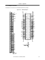
User’s Manual startWARE-GHS-Ravin-E Ravin-E Add-on Board for startWARE-GHS-VR4131 and startWARE-GHS-VR4133 Document No. U17316EE1V0UM00 Date Published September 2004 NEC Corporation 2004 Printed in Germany NOTES FOR CMOS DEVICES 1 PRECAUTION AGAINST ESD FOR SEMICONDUCTORS Note: Strong electric field, when exposed to a MOS device, can cause destruction of the gate oxide and ultimately degrade the device operation. Steps must be taken to stop generation of static electricity as much as possible, and quickly dissipate it once, when it has occurred. Environmental control must be adequate. When it is dry, humidifier should be used. It is recommended to avoid using insulators that easily build static electricity. Semiconductor devices must be stored and transported in an anti-static container, static shielding bag or conductive material. All test and measurement tools including work bench and floor should be grounded. The operator should be grounded using wrist strap. Semiconductor devices must not be touched with bare hands. Similar precautions need to be taken for PW boards with semiconductor devices on it. 2 HANDLING OF UNUSED INPUT PINS FOR CMOS Note: No connection for CMOS device inputs can be cause of malfunction. If no connection is provided to the input pins, it is possible that an internal input level may be generated due to noise, etc., hence causing malfunction. CMOS devices behave differently than Bipolar or NMOS devices. Input levels of CMOS devices must be fixed high or low by using a pull-up or pull-down circuitry. Each unused pin should be connected to V DD or GND with a resistor, if it is considered to have a possibility of being an output pin. All handling related to the unused pins must be judged device by device and related specifications governing the devices. 3 STATUS BEFORE INITIALIZATION OF MOS DEVICES Note: Power-on does not necessarily define initial status of MOS device. Production process of MOS does not define the initial operation status of the device. Immediately after the power source is turned ON, the devices with reset function have not yet been initialized. Hence, power-on does not guarantee out-pin levels, I/O settings or contents of registers. Device is not initialized until the reset signal is received. Reset operation must be executed immediately after power-on for devices having reset function. 2 Preliminary User’s Manual U17316EE1V0UM00 • The information in this document is current as of 14.09.2004. The information is subject to change without notice. For actual design-in, refer to the latest publications of NEC Electronics data sheets or data books, etc., for the most up-to-date specifications of NEC Electronics products. Not all products and/or types are available in every country. Please check with an NEC sales representative for availability and additional information. • No part of this document may be copied or reproduced in any form or by any means without prior written consent of NEC Electronics. NEC Electronics assumes no responsibility for any errors that may appear in this document. • NEC Electronics does not assume any liability for infringement of patents, copyrights or other intellectual property rights of third parties by or arising from the use of NEC Electronics products listed in this document or any other liability arising from the use of such NEC Electronics products. No license, express, implied or otherwise, is granted under any patents, copyrights or other intellectual property rights of NEC Electronics or others. • Descriptions of circuits, software and other related information in this document are provided for illustrative purposes in semiconductor product operation and application examples. The incorporation of these circuits, software and information in the design of customer's equipment shall be done under the full responsibility of customer. NEC Electronics no responsibility for any losses incurred by customers or third parties arising from the use of these circuits, software and information. • While NEC Electronics endeavors to enhance the quality, reliability and safety of NEC Electronics products, customers agree and acknowledge that the possibility of defects thereof cannot be eliminated entirely. To minimize risks of damage to property or injury (including death) to persons arising from defects in NEC Electronics products, customers must incorporate sufficient safety measures in their design, such as redundancy, fire-containment and anti-failure features. • NEC Electronics products are classified into the following three quality grades: “Standard”, “Special” and “Specific”. The "Specific" quality grade applies only to NEC Electronics products developed based on a customerdesignated “quality assurance program” for a specific application. The recommended applications of NEC Electronics product depend on its quality grade, as indicated below. Customers must check the quality grade of each NEC Electronics product before using it in a particular application. "Standard": Computers, office equipment, communications equipment, test and measurement equipment, audio and visual equipment, home electronic appliances, machine tools, personal electronic equipment and industrial robots. "Special": Transportation equipment (automobiles, trains, ships, etc.), traffic control systems, anti-disaster systems, anti-crime systems, safety equipment and medical equipment (not specifically designed for life support). "Specific": Aircraft, aerospace equipment, submersible repeaters, nuclear reactor control systems, life support systems and medical equipment for life support, etc. The quality grade of NEC Electronics products is “Standard” unless otherwise expressly specified in NEC Electronics data sheets or data books, etc. If customers wish to use NEC Electronics products in applications not intended by NEC Electronics, they must contact NEC Electronics sales representative in advance to determine NEC Electronics 's willingness to support a given application. Notes: 1. " NEC Electronics" as used in this statement means NEC Electronics Corporation and also includes its majority-owned subsidiaries. 2. " NEC Electronics products" means any product developed or manufactured by or for NEC Electronics (as defined above). M8E 02.10 Preliminary User’s Manual U17316EE1V0UM00 3 Regional Information Some information contained in this document may vary from country to country. Before using any NEC product in your application, please contact the NEC office in your country to obtain a list of authorized representatives and distributors. They will verify: • Device availability • Ordering information • Product release schedule • Availability of related technical literature • Development environment specifications (for example, specifications for third-party tools and components, host computers, power plugs, AC supply voltages, and so forth) • Network requirements In addition, trademarks, registered trademarks, export restrictions, and other legal issues may also vary from country to country. NEC Electronics America Inc. Santa Clara, California Tel: 408-588-6000 800-366-9782 Fax: 408-588-6130 800-729-9288 NEC Electronics (Europe) GmbH Duesseldorf, Germany Tel: 0211-65 03 1101 Fax: 0211-65 03 1327 Sucursal en España Madrid, Spain Tel: 091- 504 27 87 Fax: 091- 504 28 60 Succursale Française Vélizy-Villacoublay, France Tel: 01-30-67 58 00 Fax: 01-30-67 58 99 4 Filiale Italiana Milano, Italy Tel: 02-66 75 41 Fax: 02-66 75 42 99 NEC Electronics Hong Kong Ltd. Hong Kong Tel: 2886-9318 Fax: 2886-9022/9044 Branch The Netherlands Eindhoven, The Netherlands Tel: 040-244 58 45 Fax: 040-244 45 80 NEC Electronics Hong Kong Ltd. Seoul Branch Seoul, Korea Tel: 02-528-0303 Fax: 02-528-4411 Branch Sweden Taeby, Sweden Tel: 08-63 80 820 Fax: 08-63 80 388 United Kingdom Branch Milton Keynes, UK Tel: 01908-691-133 Fax: 01908-670-290 NEC Electronics Singapore Pte. Ltd. Singapore Tel: 65-6253-8311 Fax: 65-6250-3583 NEC Electronics Taiwan Ltd. Taipei, Taiwan Tel: 02-2719-2377 Fax: 02-2719-5951 Preliminary User’s Manual U17316EE1V0UM00 Preface Readers This manual is intented for users who want to understand the functions of the startWARE-GHS-Ravin-E. Purpose This manual presents the hardware manual of startWARE-GHS-Ravin-E. Organization This system specification describes the following sections: Legend • Pin function • CPU function • Internal peripheral function • Flash memory Symbols and notation are used as follows: Weight in data notation : Left is high-order column, right is low order column Active low notation : xxx (pin or signal name is over-scored) or /xxx (slash before signal name) Memory map address: : High order at high stage and low order at low stage Note : Explanation of (Note) in the text Caution : Item deserving extra attention Remark : Supplementary explanation to the text Numeric notation : Binary . . . XXXX or XXXB Decimal . . . XXXX Hexadecimal . . . XXXXH or 0x XXXX Prefixes representing powers of 2 (address space, memory capacity) K (kilo) : 210 = 1024 M (mega) : 220 = 10242 = 1,048,576 G (giga) : 230 = 10243 = 1,073,741,824 User’s Manual U17316EE1V0UM00 5 6 User’s Manual U17316EE1V0UM00 Table of Contents Preface . . . . . . . . . . . . . . . . . . . . . . . . . . . . . . . . . . . . . . . . . . . . . . . . . . . . . . . 5 Chapter 1 1.1 1.2 1.3 Chapter 2 2.1 2.2 Board Features . . . . . . . . . . . . . . . . . . . . . . . . . . . . . . . . . . . . . . . . . . . . . . . . 15 Summary of Features . . . . . . . . . . . . . . . . . . . . . . . . . . . . . . . . . . . . . . . . . . . . . . . . . . 15 Picture of startWARE-GHS-Ravin-E Board . . . . . . . . . . . . . . . . . . . . . . . . . . . . . . . . . 16 Chapter 3 3.1 Functional Description. . . . . . . . . . . . . . . . . . . . . . . . . . . . . . . . . . . . . . . . . . 17 Power Consumption . . . . . . . . . . . . . . . . . . . . . . . . . . . . . . . . . . . . . . . . . . . . . . . . . . . 18 Chapter 4 4.1 4.2 4.3 4.4 Introduction. . . . . . . . . . . . . . . . . . . . . . . . . . . . . . . . . . . . . . . . . . . . . . . . . . . 13 System Requirements . . . . . . . . . . . . . . . . . . . . . . . . . . . . . . . . . . . . . . . . . . . . . . . . . . 13 Package Contents . . . . . . . . . . . . . . . . . . . . . . . . . . . . . . . . . . . . . . . . . . . . . . . . . . . . . 13 Related Documents . . . . . . . . . . . . . . . . . . . . . . . . . . . . . . . . . . . . . . . . . . . . . . . . . . . . 13 Software Description . . . . . . . . . . . . . . . . . . . . . . . . . . . . . . . . . . . . . . . . . . . 19 Ravin-E Graphics Library . . . . . . . . . . . . . . . . . . . . . . . . . . . . . . . . . . . . . . . . . . . . . . . 19 Display of PNG Files . . . . . . . . . . . . . . . . . . . . . . . . . . . . . . . . . . . . . . . . . . . . . . . . . . . 20 Bin2C: Converting Binary Files to C-Source Code. . . . . . . . . . . . . . . . . . . . . . . . . . . 20 Demonstration Programs . . . . . . . . . . . . . . . . . . . . . . . . . . . . . . . . . . . . . . . . . . . . . . . 21 4.4.1 Animation . . . . . . . . . . . . . . . . . . . . . . . . . . . . . . . . . . . . . . . . . . . . . . . . . . . . . . 21 4.4.2 Benchmarks . . . . . . . . . . . . . . . . . . . . . . . . . . . . . . . . . . . . . . . . . . . . . . . . . . . . 22 4.4.3 Datalogger . . . . . . . . . . . . . . . . . . . . . . . . . . . . . . . . . . . . . . . . . . . . . . . . . . . . . 22 4.4.4 HW-Test . . . . . . . . . . . . . . . . . . . . . . . . . . . . . . . . . . . . . . . . . . . . . . . . . . . . . . . 22 Chapter 5 Appendix . . . . . . . . . . . . . . . . . . . . . . . . . . . . . . . . . . . . . . . . . . . . . . . . . . . . . 23 5.1 Description of Connectors and Jumpers. . . . . . . . . . . . . . . . . . . . . . . . . . . . . . . . . . . 24 5.1.1 Host Connector CN1. . . . . . . . . . . . . . . . . . . . . . . . . . . . . . . . . . . . . . . . . . . . . . 24 5.1.2 Video Connectors CN8 and CN9 . . . . . . . . . . . . . . . . . . . . . . . . . . . . . . . . . . . . 27 5.1.3 VGA Connector CN12 . . . . . . . . . . . . . . . . . . . . . . . . . . . . . . . . . . . . . . . . . . . . 28 5.1.4 Digital video output connector CN13 . . . . . . . . . . . . . . . . . . . . . . . . . . . . . . . . . 29 5.1.5 JTAG interface connector CN14. . . . . . . . . . . . . . . . . . . . . . . . . . . . . . . . . . . . . 31 5.1.6 Disable Video Processor with JP1 . . . . . . . . . . . . . . . . . . . . . . . . . . . . . . . . . . . 32 5.1.7 Select CS input with JP2 . . . . . . . . . . . . . . . . . . . . . . . . . . . . . . . . . . . . . . . . . . 32 5.1.8 Select digital video signal voltage with JP3 . . . . . . . . . . . . . . . . . . . . . . . . . . . . 33 5.1.9 Enable DOTCLK for VGA interface with JP4 . . . . . . . . . . . . . . . . . . . . . . . . . . . 33 5.2 Address Map . . . . . . . . . . . . . . . . . . . . . . . . . . . . . . . . . . . . . . . . . . . . . . . . . . . . . . . . . 34 5.3 startWARE-GHS-Ravin-E Schematics . . . . . . . . . . . . . . . . . . . . . . . . . . . . . . . . . . . . . 35 5.4 PCI Adapter Schematics . . . . . . . . . . . . . . . . . . . . . . . . . . . . . . . . . . . . . . . . . . . . . . . . 37 User’s Manual U17316EE1V0UM00 7 8 User’s Manual U17316EE1V0UM00 List of Figures Figure 2-1: Figure 3-1: Figure 5-1: Figure 5-2: Figure 5-3: Figure 5-4: Figure 5-5: Figure 5-6: Figure 5-7: Figure 5-8: Figure 5-9: Figure 5-10: Figure 5-11: Figure 5-12: Figure 5-13: startWARE-GHS-Ravin-E Board ................................................................................. 16 startWARE-GHS-Ravin-E Block Diagram ................................................................... 17 Board Outline and Component Placement .................................................................. 23 Host Connector CN1 ................................................................................................... 24 Video Connectors CN8 and CN9 ................................................................................ 27 VGA Connector CN12 ................................................................................................. 28 Digital video output connector CN13 ........................................................................... 29 JTAG interface connector CN14 ................................................................................. 31 Jumper JP1 ................................................................................................................. 32 Jumper JP2 ................................................................................................................. 32 Jumper JP3 ................................................................................................................. 33 Jumper JP4 ................................................................................................................. 33 Ravin-E........................................................................................................................ 35 Connectors .................................................................................................................. 36 VME-PCI Adapter ........................................................................................................ 37 User’s Manual U17316EE1V0UM00 9 10 User’s Manual U17316EE1V0UM00 List of Tables Table 3-1: Table 5-1: Table 5-2: Table 5-3: Table 5-4: Table 5-5: Table 5-6: Table 5-7: Operating Currents under typical operating conditions .................................................. 18 Technical Data of the Ravin-E Board ............................................................................. 23 Host Connector CN1 ...................................................................................................... 24 VGA Connector CN12 .................................................................................................... 28 Digital video output connector CN13 .............................................................................. 30 JTAG interface connector CN14..................................................................................... 31 Jumper Settings with JP2 ............................................................................................... 32 Jumper Settings with JP3 ............................................................................................... 33 User’s Manual U17316EE1V0UM00 11 12 User’s Manual U17316EE1V0UM00 Chapter 1 Introduction 1.1 System Requirements Motherboard: startWARE-GHS-Ravin-E is an add-on board designed for the startWARE-GHSVR4131/33 boards. Running the startWARE-GHS-Ravin-E board with other motherboards will require a suitable adapter, which is not part of this package. Such adapters are not available from NEC and therefore have to be provided by the user. Alternatively the startWARE-GHS-Ravin-E board can be operated via its PCI interface. That will require a suitable adapter whose schematics are included in chapter 5.4 of this document. Note that the PCI interface uses 3 V signaling only and it can therefore not be operated in a normal PC. 1.2 Package Contents Please verify that you have received all parts listed in the package contents list attached to the startWARE-GHS-Ravin-E package. If any part is missing or seems to be damaged, please contact the dealer from whom you purchased your startWARE-GHS-Ravin-E. Note: Updates to this User Manual, additional documentation and/or utilities for startWARE-GHS-Ravin-E, if available, may be downloaded from the NEC WEB page(s): http://www.nec.de/support. 1.3 Related Documents Ravin-E Preliminary Data Sheet, NEC Doc. Number S15521EJ1V0DS00 startWARE-GHS-VR4131 User’s Manual, NEC Doc. Number U16417EE1V0UM00 startWARE-GHS-VR4133 User’s Manual, NEC Doc. Number U16916EE2V0UM00 Application Note: Operation of Ravin-E with V850 Devices NEC Doc. Number S17194EE1V0AN00 User’s Manual U17316EE1V0UM00 13 [MEMO] 14 User’s Manual U17316EE1V0UM00 Chapter 2 Board Features As the name implies, the startWARE-GHS-Ravin-E board employs the Ravin-E display controller (µPD72255) as its centrepiece. Also implemented is an SAA7113H or SAF7113H video processor, which is used to digitize a PAL or NTSC standard video signal and optionally overlay it on the graphics. An analogue display can be connected via a standard 15-pin high density DSUB connector, while a digital display connects through a 30-pin row connector. The startWARE-GHS-Ravin-E board has been designed as an add-on board for the startWARE-GHS-VR4131 or startWARE-GHS-VR4133 boards. It connects to these boards through a 96-pin male DIN connector CN1, which also carries the 5 V DC power supply. 2.1 Summary of Features • Ravin-E (µPD72255) graphics display controller • 64 MB on board SDRAM frame buffer • Enhanced SAA7113 video processor for video capture • Analogue (0.7 VPP) and digital (3.3 V or 5 V) video outputs • All Ravin-E signals available on standard logic analyzer connectors • Single 5 V power supply (provided from main board) • JTAG boundary scan implemented User’s Manual U17316EE1V0UM00 15 Chapter 2 Board Features 2.2 Picture of startWARE-GHS-Ravin-E Board Figure 2-1: 16 startWARE-GHS-Ravin-E Board User’s Manual U17316EE1V0UM00 Chapter 3 Functional Description Ravin-E (µPD72255Y) is the successor of the Ravin (µPD72254Y) display controller, designed for use in car navigation, multimedia and passenger entertainment systems. In addition to the original display control and drawing functions of µPD72254Y, Ravin-E supports high quality alpha blending for all window layers. This alpha blending feature is also employed for anti-aliased line drawing. Ravin-E also provides a function for capturing and displaying external video signals as well as a built-in D/A converter for analogue CRT or TFT displays. Ravin-E can be connected to virtually any 32-bit host CPU with an asynchronous SRAM-like bus interface. A second 32-bit wide data bus connects to standard SDRAMs which serve as the frame buffer for the graphics and the video. startWARE-GHS-Ravin-E Block Diagram SAA7113H 96-pin DIN to host CPU board Figure 3-1: 8-bit 256 Mb x 16 Ravin-E µPD72255 digital 3 V / 5 V buffers digital RGB 256 Mb x 16 analogue video drivers analogue RGB As shown in the above block diagram, Ravin-E connects through a 96-pin DIN connector to the host CPU platform. This platform will be typically equipped with a VR41xx MIPS-RISC CPU, but it may be adapted to any other CPU with a suitable SRAM-like interface. The signal levels are 3.3 V LVTTL and the pinout is defined in “Host Connector CN1” on page 24 of the appendix. Ravin-E is connected to two 256 Mbit SDRAMs, each one of them being 16-bit wide. These SDRAMs are primarily employed as frame buffer for the graphics, as video buffer for the overlaid video and also to store bitmaps, which can then be transferred quickly to the active screen location. The SDRAM also holds the alpha values when alpha blending is used and the z-values in case of 3-D applications. Even though the interface is not bandwidth optimized, the CPU has direct access to all locations in the SDRAM and therefore it might make use of any otherwise unused memory locations. The SAA7113H or SAF7113H enhanced video processor digitizes one of two incoming analogue composite video signals (PAL or NTSC standard) and converts it to a standard 8-bit wide ITU 656 compliant YUV 4:2:2 signal. That signal can be captured by Ravin-E, optionally scaled up or down and then stored in the SDRAM. In the video output path, the format can be converted on the fly from YUV to RGB. See the SAA7113H Product Specification from Philips and the Ravin-E Data Sheet for details. User’s Manual U17316EE1V0UM00 17 Chapter 3 Functional Description The startWARE-GHS-Ravin-E board provides two display outputs, each of which conveys the same display contents. 75 Ω RGB video drivers are provided on board, so that a 0.7 VPP monitor can be directly connected to CN12. 5 V TTL compatible sync signals are provided as well on this connector. The dot clock can optionally be enabled on this connector via jumper JP4. Note that this connection is not required for standard VGA monitors and it might even cause problems. Therefore JP4 is normally unconnected. Check your monitor specification before setting JP4. JP4 may be useful when connecting an analog TFT display to this connector. CN13 connects to a digital display, usually a TFT. Along with the digital colour, CN13 provides the sync and the dot clock signals, as well as a few control signals for the TFT display. JP3 switches the interface voltage between 3.3 V LVTTL and 5.0 V TTL. CN13 also provides the 5 V and 3.3 V operating voltages. See the chapter on power consumption below for details on the current ratings. Three LEDs are provided to quickly check the operating voltages. D1 connects to the externally supplied 5 V, D2 to the 3.3 V and D3 to the 2.5 V. The 3.3 V and the 2.5 V are locally generated on the startWARE-GHS-Ravin-E board. When power is supplied, then all these LEDs should light up with about the same intensity. CN14 is a connector for JTAG boundary scan equipment. The SAF7113H is the first device in the scan chain, while Ravin-E is the second one. 3.1 Power Consumption The startWARE-GHS-Ravin-E board is supplied with a single +5 V DC operating voltage from the main board. The internally required 3.3 V and 2.5 V are generated by linear voltage regulators on the Ravin-E board. The following table shows the operating currents that have been measured under typical operating conditions (capturing video input and displaying it along with graphics). Note that these are reference values of just one board and that other boards may show slightly different current consumption, even if the conditions are the same. Table 3-1: Operating Currents under typical operating conditions Voltage Measured current Design limitNote 2 5V 500 mANote 1 1000 mA VCC3.3 160 mA 400 mA VCC2.5 230 mA 300 mA AVDD2 36 mA 100 mA Notes: 1. Estimated, not measured (includes current for VCC3.3, VCC2.5 and AVDD2) 2. Do not permanently exceed these limits (e.g. by external loads) The measured values include the power consumption of the respective voltage regulator, which is negligible. The voltage regulators have shunt resistors at their input voltage pin. These resistors can serve well for current consumption measurements, but their other purpose is to burn away some of the power, so that only part of it is dissipated in the regulator itself. The VCC3.3 voltage regulator (IC8) along with its shunt resistors and its heat sink on the PCB is designed to source up to 400 mA. Therefore it can supply external circuits (e.g. a suitable TFT Display) as long as they do not draw more than about 250 mA. Take care not to couple external noise onto this supply rail. 18 User’s Manual U17316EE1V0UM00 Chapter 4 Software Description We have written a few demo programs, which can be found in the “Software\Ravin-E” directory of the startWARE-GHS-Ravin-E CD. The programs can be compiled for MIPS RISC devices or for V850E devices. Build files for each of these environments are supplied. We have used Green Hills version 3.5.1 for V850 and version 3.6.1 for MIPS. Make sure to issue a “build all” command, if you change between these tool chains. Otherwise the tools may mix modules of different architectures, which may lead to some weird error messages. Here is the directory structure of Software\Ravin-E: Animation Benchmarks Bin2C Datalogger HW-Test Include LibV850 LibVR MyLib png rgl StartupVR The individual demo programs and their build files are found in Animation, Benchmarks, Datalogger and HW-Test. Bin2C contains a Windows application program, which converts a file to C-Source code. These programs are described later in this chapter. The Include directory contains a few include files, which are required by the demo programs and the libraries. LibV850 and LibVR contain the compiled libraries for the respective tool chain. MyLib holds the sources of the CPU initialization code and the interface code for the PNG library. png contains the sources of the png library (libpng) and the zlib, which is required for libpng. Both are third party software packages. See http://www.libpng.org/ for the latest sources. rgl contains the Ravin Graphics Library and StartupVR contains startup code for MIPS devices and defines for the VR4131. All libraries can be built automatically by the build files in LibVR or LibV850. The libraries are supplied on the CD and ready to use, but it may be useful to download the latest libpng and zlib sources from the internet and recompile them. All temporary files during the build process are stored in the Tmp subdirectories of the respective module. The files in this path can be deleted after the build process. 4.1 Ravin-E Graphics Library The Ravin-E graphics library (RGL) provides higher level functions to initialize and operate Ravin-E. Only the function ghs\rgl_custom.c needs to be adapted, when rgl is ported to another target. It defines the addresses of the Ravin-E registers (PhysReg) and of the Ravin-E frame buffer (PhysFB). An os_sleep(n) function is required for delays and timeouts, which delays by roughly n milliseconds. It needs not be very precise. For the V850E/ME2, we have implemented a simple active delay, which delays roundabout 1 ms for a 150 MHz device. If the CPU core frequency differs much from that, it should be adapted accordingly. A built-in timer is used for the VR4131, which generates 1 ms interrupts. The respective code is located in StartupVR\iqueue.c, start.mip and isr.mip. A detailed description of the RGL can be found in the “Ravin-E Graphics Library Manual” in the rgl\doc directory. User’s Manual U17316EE1V0UM00 19 Chapter 4 Software Description 4.2 Display of PNG Files In order to display png files (Portable Network Graphics), we have ported the free PNG Reference Library libpng (www.libpng.org) to the V850. This library requires the zlib compression library (www.gzip.org), which has also been ported. These two libraries are documented on their respective websites. Calls to zlib functions are transparent and the libpng user need not bother too much about that zlib library. It should be noted, however, that a certain amount of heap space is required for both libpng and zlib. Also the stack size should not be too small, as these functions seem to use it extensively. They have clearly been written with personal computers in mind and are not optimized for the limited memory resources of embedded applications. Nevertheless there is a limited number of tuning possibilities by defining certain variables that control compilation of the libraries. See the respective documentation for details. 4.3 Bin2C: Converting Binary Files to C-Source Code A binary file cannot be directly copied to an embedded system. At least it must be converted to a downloadable ASCII file of Intel-Hex or Motorola S-Record format. A slightly more complicated conversion seems to offer the best possible flexibility: converting the binary file to C-Source code. That is exactly what the bin2c utility was made for. The generated C-Source code can be embedded into any project and be located to any required address. bin2c was written for the conversion of .png files, but it does not perform any structural analysis and so it may be used with any file, not just with binary png-files. bin2c inserts a pragma for the Green Hills compiler to emit the subsequent data into the segment .images. That allows for relocation of that data to any target address. bin2c defines an array of unsigned char and names the array with the file name of the input file. A few characters are converted if they are incompatible with the C naming conventions. The best idea is probably to avoid file names, which do not comply with C variable names. bin2c can convert multiple files at once. For each input file it creates its own array with a name as described before. When the “Generate table of contents” checkbox is enabled, then an array of pointers to unsigned char is allocated and that array is initialized with pointers to the individual arrays. The name of this table is toc and the variable toc_size is initialized with the number of arrays (=number of files). Animated sequences are usually created with index numbers in their file names. When the “Sort Input Files” checkbox is enabled, then the files are automatically sorted in ascending file name order. bin2c was compiled with the free OpenWatcom tool chain, which is downloadable from http://www.openwatcom.org/. The sources of bin2c are provided on the CD and may be modified as required. 20 User’s Manual U17316EE1V0UM00 Chapter 4 Software Description 4.4 Demonstration Programs Four rather simple demo programs are supplied on the startWARE-GHS-Ravin-E CD. They are described in this paragraph. 4.4.1 Animation Animation is a demo program which displays a rotating image on the screen. This endless movie is simply made by displaying a sequence of 60 PNG images cyclically, so that the impression of a movie is generated. The images were produced by POVRay (www.povray.org) and ThumbsPlus (www.thumbsplus.com) was used to generate a common palette for all of them. A common palette is required to eliminate the temporal noise, which would otherwise occur due to the asynchronous update of the palette and the display data. One of two implementations can be selected at compile time. If REALTIME_DECODE is defined, then each individual frame is decoded and the result is directly copied to the Ravin-E frame buffer. That saves RAM space, but the decoding has to be repeated as often as the image is to be displayed. Decoding a png file is rather time consuming. With this option enabled, the rotation of the image is rather slow and not at all smooth. If the option PRE_DECODE is enabled, then all frames are decompressed before the animation starts. The decompressed data is stored in the heap space, which must therefore be sufficiently large to hold all decoded files. Each image of this example has a size of 240x240 pixels and the images use a colour palette, which means that they use 8 bits per pixel. The required heap space for a single frame is thus 57600 bytes which sums up to almost 3.5 MB for all frames. Therefore the total heap space should be at least 4 MB. Pre-decoding takes a few seconds and when it is done, the animation starts. It merely copies the individual decompressed frames from the heap to the frame buffer, which is very quick. Therefore this version needs a delay after each frame is sent to the frame buffer. We have decided for 15 ms, which makes the rotation rather smooth. The performance and the required CPU time could be further improved by copying the decompressed individual images into Ravin-E's frame buffer instead of the heap. The total size of the frame buffer on the startWARE-GHS-Ravin-E board is 64 MB which is plenty of space outside the current display area. Transfer of the image to the screen location would then be accomplished by a BITBLT command to Ravin-E. For the CPU that is a simple sequence of a few register write operations and as such it would virtually cost no CPU time at all. User’s Manual U17316EE1V0UM00 21 Chapter 4 Software Description 4.4.2 Benchmarks Benchmarks is a program to test the performance of Ravin-E and the bus interface. It tests the speed of vector and filled rectangle drawing as well as the data transfer between the host and Ravin-E. Benchmarks measures certain key performance values under real-life rather than optimized idealistic conditions. The selected screen resolution is 800 x 600 pixel at 60 Hz frame rate and two display layers are enabled, one with 16 bit per pixel and the other one with 8 bit per pixel. In this configuration, the screen refresh uses approximately 25% of the available bandwidth between Ravin-E and its SDRAMs. This is an average bus load calculated for a whole frame and it includes the sync pulses, during which no data transfer takes place at all. The average data rate during the display of a scan line is about twice as high with short periods of essentially 100% bus load when a burst read is issued to fill the video output pipeline. The times are measured with built-in timers on the V850E/ME2 and on the VR4131. The VR4131 timer does not detect overflows and the arithmetic has been chosen to make a compromise between precision and integer overflow in intermediate results. Therefore when changing the code, especially the number of loops, note that overflows on the VR4131 are not detected and they may return invalid results. Also the timers are configured for the documented operating speeds. Make sure to adapt the initialization, if the clock speed deviates from the reference clock speed. Note that the results of the timing measurements vary in a certain range due to the statistical nature of the accesses on the Ravin-E frame buffer. The effect of write combining can be tested by defining NO_WC at compile time. Write combining is enabled by default. It enables Ravin-E to combine write transfers to subsequent memory addresses and to make burst accesses instead of single writes. That has a very noticeable effect if data is usually written to subsequent addresses. Writes to random addresses are slowed down, however, because every individual write access is delayed, as it might have to be combined with the next write. 4.4.3 Datalogger Datalogger is an application, which displays a simple four channel datalogger grid on the foreground layer. This is a pre-defined image that is stored in a PNG-file and extracted once at initialization time into the frame buffer. Four traces are displayed on the background layer, which move from the right side to the left, so that the older values appear on the left and the newer values on the right side. The displayed values are generated from pseudo random numbers which are low pass filtered to make them look like real analogue input data. Display of the trace lines makes use of Ravin-E's feature to move the viewport freely over the virtual display area. When the display line wraps over, Ravin-E does not actually display the image data from the subsequent line, but the data from the beginning of the current line. This feature permits the impression of a moving image, without actually copying data within the frame buffer. Only the start address of the viewport is constantly updated. In the case of the datalogger demo program, the right most column is updated in addition to the viewport address, as always new data shall be displayed. The display data is erased on the left side of the screen, before it enters the outside of the grid. The datalogger demo program requires very little CPU performance. Almost all CPU time is spent in the “os_sleep(20)” delay at the end of function main. 4.4.4 HW-Test HW-Test is a program, which is used by NEC in the startWARE-GHS-Ravin-E production test. It performs an initial test of the Ravin-E frame buffer memory, displays some vectors with colour shading on the screen and captures a video via the cinch connectors. 22 User’s Manual U17316EE1V0UM00 Chapter 5 Appendix This chapter collects the technical data of the board. Detailed explanations are therefore reduced to a minimum. Figure 5-1: Board Outline and Component Placement JP1 D1/2/3 deselect video processor LEDs for 5.0 V/3.3 V/2.5 V CN13 digital Video output CN8 Video in 1 CN14 JTAG interface CN9 Video in 2 JP4 JP3 enable DOTCLK 3.3 V/ 5 V select for digital out CN12 JP2 analogue VGA monitor CS select CN1 Host connector Table 5-1: Technical Data of the Ravin-E Board Component See page Type CN1 page 24 DIN41612, male, 3 × 32 pins Connector to host CPU board CN8 page 27 Cinch Video 1 input CN9 page 27 Cinch Video 2 input CN12 page 28 DSUB15, female, high-density VGA monitor, analogue video output CN13 page 29 Row connector, male, 2 × 15 pins Digital video output CN14 page 31 Row connector, male, 2 × 5 pins JTAG interface JP1 page 32 Row connector, male, 2 pins De-select video processor JP2 page 32 Row connector, male, 3 pins Select one of two chip select inputs JP3 page 33 Row connector, male, 3 pins Select digital video interface voltage JP4 page 33 Row connector, male, 2 pins Enable DOTCLK output on CN12 D1/D2/D3 - LED 5.0 V, 3.3 V, 2.5 V operating voltages User’s Manual U17316EE1V0UM00 Purpose 23 Chapter 5 Appendix 5.1 Description of Connectors and Jumpers 5.1.1 Host Connector CN1 The a- and c-rows of the connector are exchanged against each other in the schematics and on the silk screen of the board. Unlike the schematics, the following table lists the real connection of the signals with the pin numbers according to common practice and according to the pin number imprint on the connector. Figure 5-2: Table 5-2: Host Connector CN1 Host Connector CN1 (1/4) Number Name DirectionNote a1 VCC50 in +5 V DC +/-10% power supply from motherboard b1 VCC50 in +5 V DC +/-10% power supply from motherboard c1 VCC50 in +5 V DC +/-10% power supply from motherboard a2 DATA30 in/out data bus signal 30 b2 DATA31 in/out data bus signal 31 c2 GND in a3 DATA27 in/out data bus signal 27 b3 DATA28 in/out data bus signal 28 c3 DATA29 in/out data bus signal 29 a4 DATA24 in/out data bus signal 24 b4 DATA25 in/out data bus signal 25 c4 DATA26 in/out data bus signal 26 a5 DATA22 in/out data bus signal 22 b5 DATA23 in/out data bus signal 23 c5 GND in a6 DATA19 in/out Description ground ground data bus signal 19 Note: Signal direction as seen from startWARE-GHS-Ravin-E board (e.g. “in” is an input on this board and must be driven by the main board) 24 User’s Manual U17316EE1V0UM00 Chapter 5 Table 5-2: Appendix Host Connector CN1 (2/4) Number Name DirectionNote b6 DATA20 in/out data bus signal 20 c6 DATA21 in/out data bus signal 21 a7 DATA16 in/out data bus signal 16 b7 DATA17 in/out data bus signal 17 c7 DATA18 in/out data bus signal 18 a8 DATA14 in/out data bus signal 14 b8 DATA15 in/out data bus signal 15 c8 GND in a9 DATA11 in/out data bus signal 11 b9 DATA12 in/out data bus signal 12 c9 DATA13 in/out data bus signal 13 a10 DATA8 in/out data bus signal 8 b10 DATA9 in/out data bus signal 9 c10 DATA10 in/out data bus signal 10 a11 DATA6 in/out data bus signal 6 b11 DATA7 in/out data bus signal 7 c11 GND in a12 DATA3 in/out data bus signal 3 b12 DATA4 in/out data bus signal 4 c12 DATA5 in/out data bus signal 5 a13 DATA0 in/out data bus signal 0 b13 DATA1 in/out data bus signal 1 c13 DATA2 in/out data bus signal 2 a14 BEB1 in Byte Enable 1 (active low) b14 BEB0 in Byte Enable 0 (active low) c14 GND in ground a15 GND in ground b15 BEB3 in Byte Enable 3 (active low) c15 BEB2 in Byte Enable 2 (active low) a16 n.c. - unconnected b16 n.c. - unconnected c16 RESET in Reset signal (active high) a17 ADD22 in address bus signal 22 b17 ADD23 in address bus signal 23 c17 GND in ground a18 ADD19 in address bus signal 19 b18 ADD20 in address bus signal 20 c18 ADD21 in address bus signal 21 a19 ADD16 in address bus signal 16 b19 ADD17 in address bus signal 17 Description ground ground Note: Signal direction as seen from startWARE-GHS-Ravin-E board (e.g. “in” is an input on this board and must be driven by the main board) User’s Manual U17316EE1V0UM00 25 Chapter 5 Table 5-2: Appendix Host Connector CN1 (3/4) Number Name DirectionNote c19 ADD18 in address bus signal 18 a20 ADD14 in address bus signal 14 b20 ADD15 in address bus signal 15 c20 GND in ground a21 ADD11 in address bus signal 11 b21 ADD12 in address bus signal 12 c21 ADD13 in address bus signal 13 a22 ADD8 in address bus signal 8 b22 ADD9 in address bus signal 9 c22 ADD10 in address bus signal 10 a23 ADD6 in address bus signal 6 b23 ADD7 in address bus signal 7 c23 GND in ground a24 ADD3 in address bus signal 3 b24 ADD4 in address bus signal 4 c24 ADD5 in address bus signal 5 a25 n.c. - unconnected b25 RDY out CPU Ready signal (active high, i.e. low=wait, high=ready); high impedance while Ravin-E is not selected. c25 ADD2 in address bus signal 2 a26 LCS1B in Chip select 1 (active low) b26 LCS0B in Chip select 0 (active low) c26 GND in ground a27 RDB in CPU read signal (active low) b27 WRB in CPU write signal (active low) c27 GND in ground a28 n.c. - unconnected b28 n.c. - unconnected c28 n.c. - unconnected a29 DAKB in Data acknowledge b29 DRQB out Data request c29 RDSTSB out Read status a30 n.c. - unconnected b30 CPUSEL in Select CPU interface (0=PCI, 1=asynchronous) c30 n.c. - unconnected a31 GND in ground b31 PCICLK in PCI clock (connect to GND if asynchronous interface) c31 GND in ground a32 n.c. - unconnected Description Note: Signal direction as seen from startWARE-GHS-Ravin-E board (e.g. “in” is an input on this board and must be driven by the main board) 26 User’s Manual U17316EE1V0UM00 Chapter 5 Table 5-2: Appendix Host Connector CN1 (4/4) Number Name DirectionNote b32 IDSEL/ VSSEL in Initialization device select (in PCI mode) CPU interface select (in asynchronous bus mode) 0: VR41xx mode; 1: BEBn inputs are write strobe signals c32 n.c. - unconnected Description Note: Signal direction as seen from startWARE-GHS-Ravin-E board (e.g. “in” is an input on this board and must be driven by the main board) 5.1.2 Video Connectors CN8 and CN9 Standard Cinch connectors are used to input the composite video signals for the two video channels 1 and 2. The nominal impedance for each video input is 75 Ω. The signals are AC coupled to the video processor via 47 nF capacitors. The nominal video signal voltage level is 1 VPP, but due to the automatic gain adjustment within the video processor, signal levels between 0.5 VPP and 1.4 VPP are acceptable. Figure 5-3: Video Connectors CN8 and CN9 User’s Manual U17316EE1V0UM00 27 Chapter 5 Appendix 5.1.3 VGA Connector CN12 CN12 is a 15-pin female high density Sub-D connector. It has a pin configuration so that a standard VGA monitor can be connected. The RGB signal voltages have levels between 0 and 0.7 VPP, while the synchronization signals are 5 V TTL compatible. 28 Figure 5-4: VGA Connector CN12 Table 5-3: VGA Connector CN12 Number Name Direction Description 1 Red out Red colour component; 0 to 0.7 VPP 2 Green out Green colour component; 0 to 0.7 VPP 3 Blue out Blue colour component; 0 to 0.7 VPP 4 n.c. - unconnected 5 GND - Signal ground 6 n.c. - unconnected 7 n.c. - unconnected 8 n.c. - unconnected 9 DOTCLK out 10 n.c. - unconnected 11 n.c. - unconnected 12 n.c. - unconnected 13 HSYNC out Active low horizontal sync 14 VSYNC out Active low vertical sync 15 n.c. - DOTCLK if JP4 is set, otherwise unconnected unconnected User’s Manual U17316EE1V0UM00 Chapter 5 Appendix 5.1.4 Digital video output connector CN13 CN13 carries the signals for a digital TFT display. Its signal output voltages are selectable by JP3 to 3.3 V or 5 V. Figure 5-5: Digital video output connector CN13 User’s Manual U17316EE1V0UM00 29 Chapter 5 Table 5-4: Appendix Digital video output connector CN13 Number Name Direction Description 1 FSC out Ravin-E FSC outputNote 2 PLLREF out Ravin-E PLLREF outputNote 3 VCC33 - 3.3 V power supply 4 VCC50 - 5.0 V power supply 5 VO0 out Blue 1 6 VO1 out Blue 2 7 VO2 out Blue 3 8 VO3 out Blue 4 9 VO4 out Blue 5 10 GND - Ground 11 VO5 out Green 0 12 VO6 out Green 1 13 VO7 out Green 2 14 VO8 out Green 3 15 VO9 out Green 4 16 VO10 out Green 5 17 GND - Ground 18 VO11 out Red 1 19 VO12 out Red 2 20 VO13 out Red 3 21 VO14 out Red 4 22 VO15 out Red 5 23 VCC33 - 24 CSYNC out Ravin-E CSYNC# output (Note) 25 HSYNC out Ravin-E HSYNC# output (Note) 26 VSYNC out Ravin-E VSYNC# output (Note) 27 DOTCLK out Ravin-E DCLK output (Note) 28 ENABLE out Ravin-E ENABLE output (Note) 29 GND - Ground 30 GND - Ground 3.3 V power supply Note: These output pins are disabled after reset. The meaning of the output pins can be defined in the Ravin-E register VoSyncSelect at address 0x01FF FB4Ch. 30 User’s Manual U17316EE1V0UM00 Chapter 5 Appendix 5.1.5 JTAG interface connector CN14 CN14 is the JTAG interface connector. The scan chains of the SAA7113 and Ravin-E are linked, with the SAA7113 being the first in the chain and Ravin-E the second. Figure 5-6: JTAG interface connector CN14 Table 5-5: JTAG interface connector CN14 Number Name Direction Description 1 TCK in JTAG clock 2 GND - Signal ground 3 TDO out 4 VCC33 - 3.3 V power supply 5 TMS in JTAG scan chain mode select 6 n.c. - Not connected 7 TRST in JTAG scan chain tri-state 8 n.c. - Not connected 9 TDI in JTAG scan chain input 10 GND - Signal ground JTAG scan chain output User’s Manual U17316EE1V0UM00 31 Chapter 5 Appendix 5.1.6 Disable Video Processor with JP1 When a jumper is plugged onto JP1, then the video processor is de-selected. This feature has been implemented so that an external video processor can access the video input port of Ravin-E. JP1 is normally not used. Therefore the board is shipped without this jumper and thus the video processor is enabled by default. Figure 5-7: Jumper JP1 5.1.7 Select CS input with JP2 The host connector CN1 carries two chip select signals, which can be alternatively used to select Ravin-E. JP2 selects the active CS signal. Figure 5-8: Table 5-6: Jumper JP2 Jumper Settings with JP2 Jumper setting Function 1-2 (leftNote) CS0 input used 2-3 (rightNote) CS1 input used Note: Board orientation as depicted in Figure 5-1. 32 User’s Manual U17316EE1V0UM00 Chapter 5 Appendix 5.1.8 Select digital video signal voltage with JP3 The digital video output signals on CN13 can drive either 3.3 V LVTTL or 5 V TTL compatible devices. JP3 selects between these two voltages. Figure 5-9: Table 5-7: Jumper JP3 Jumper Settings with JP3 Jumper setting Function 1-2 (topNote) 3.3 V signal output level 2-3 (bottomNote) 5.0 V signal output level Note: Board orientation as depicted in Figure 5-1. 5.1.9 Enable DOTCLK for VGA interface with JP4 When a jumper is plugged onto JP4, then the 5 V TTL DOTCLK is connected to pin 9 of CN12. This signal is normally not used and therefore the board is shipped without JP4. Before plugging JP4, please make sure that your monitor can tolerate that signal. There is probably no standard monitor, which can use the DOTCLK. We have implemented it primarily for experimenting with analogue TFT displays. Figure 5-10: Jumper JP4 User’s Manual U17316EE1V0UM00 33 Chapter 5 Appendix 5.2 Address Map Ravin-E occupies 16 MB (when using the SRAM-like bus interface) or 32 MB (when using the PCI-interface) in the address space of the host CPU. In both cases, the upper 8 kB of this range are reserved for the on-chip status and command registers, while the rest of these address spaces is directly mapped to access the frame buffer. Even though the host interface is limited to 16 or 32 MB access size at a time, Ravin-E can access a total frame buffer of up to 64 MB. The window that is visible from the host CPU can be moved over the total frame buffer by specifying the frame buffer start address in the HostCpuBaseAddr. The start address is aligned to a 2 kB base address. When the startWARE-GHS-Ravin-E board is used together with the startWARE-GHS-VR4131 board, then the following address mapping in the VR4131 I/O address space applies: JP2 selects CS0: JP2 selects CS1: 0x0A00 0000 ~ 0x0AFF FFFF 0x0C00 0000 ~ 0x0CFF FFFF See page 32 for JP2 settings. Note that the sizes of the VR4131 I/O address spaces are 32 MB each, and therefore the above 16 MB address spaces are mirrored at 0x0B00 0000 ~ 0x0BFF FFFF and 0x0D00 0000 ~ 0x0DFF FFFF respectively. 34 User’s Manual U17316EE1V0UM00 FC1 2 24.576MHz X1 OUT 3 GND 1 VCC R9 R6 1 2 2200pF/25VDC/6A 10uH/180mA l1 CN9 Signal 2 3 Signal1 1 R7 R8 4.7k R38 R39 C3 47 47nf/50V/eia0603 15 C2 47nf/50V/eia0603 47 15 3.3 VCC3.3S 0 R4 AOUT AI11 AI12 AI21 AI22 32 XTALI 31 XTAL 5 AI1D 44 AI2D 9 4 7 43 1 IC1 JP1 AGND VSSA0 VSSA1 VSSA2 VSSDE1 VSSDE2 VSSDI SAF7113H 6 11 2 41 16 35 28 TDI1 38 TDI TCK 37 TCK TMS 39 TMS 8 TRST_n TDO1 36 TDO 0 R5 TP/smd TP11 C56 PCICLK 2pins 100nf/16V/eia0603 AVDD 10 3 42 18 34 33 29 R14 LLC 17 RTS1 27 33 RTS0 26 SCL 24 SDA 23 RTCO RTCO 25 VDDA0 VDDA1 VDDA2 VDDDE1 VDDDE2 VDDDA VDDDI C23 100nf/16V/eia0603 C24 RTS1 RTS0 2-D5 2-D6 2-D6 2-D6 2-D5 R10 1k 1k R11 4.7k R12 4.7k VCC3.3 R13 2-D5 R20 R19 10k R18 10k R17 10k R16 10k 10k VID(8) 22 VID(15:0) 21 VID(9) 2-D6 20 VID(10) VID(11) 19 15 VID(12) 14 VID(13) 13 VID(14) 12 VID(15) CE 40 VPO0 VPO1 VPO2 VPO3 VPO4 VPO5 VPO6 VPO7 R61 NOT ass 75 4.7k R40 100nf/16V/eia0603 GND C65 33pf/50V/eia0603 75 C6 GND 1nf/50V/eia0603 C59 VCC3.3 C4 100nf/16V/eia0603 C5 R62 33pf/50V/eia0603 C7 C9 100nf/16V/eia0603 C49 100nf/16V/eia0603 2 C57 100nf/16V/eia0603 33pf/50V/eia0603 C19 100nf/16V/eia0603 47nf/50V/eia0603 CN8 Signal 2 3 Signal1 1 C66 1 C58 VCC3.3 2-D5>2 AVDD2 N1 F3 F2 E1 F1 E4 SCL VID0 VID1 VID2 VID3 VID4 VID5 VID6 VID7 VID8 VID9 VID10 VID11 VID12 VID13 VID14 VID15 RESETB TDI TDO TCK TMS TRST AVDD1 D2 AVDD2 E17 AVDD3 R5 AVDD4 V6 DVDD2 IC4 Ravin-E/uPD72255 WRB RDB CSB RDY RDSTSB DRQB DACKB PCICLK IDSEL CPUSEL BEB0 BEB1 BEB2 BEB3 A2 A3 A4 A5 A6 A7 A8 A9 A10 A11 A12 A13 A14 A15 A16 A17 A18 A19 A20 A21 A22 A23 AD0 AD1 AD2 AD3 AD4 AD5 AD6 AD7 AD8 AD9 AD10 AD11 AD12 AD13 AD14 AD15 AD16 AD17 AD18 AD19 AD20 AD21 AD22 AD23 AD24 AD25 AD26 AD27 AD28 AD29 AD30 AD31 SCL L5 SDA L4 VCLK L3 VCSYNC M1 VID(0) G1 VID(1) H5 VID(2) H2 VID(3) H3 VID(4) H1 VID(5) H4 VID(6) J2 VID(7) J3 VID(8) J1 VID(9) J5 VID(10) J4 VID(11) K1 VID(12) K4 VID(13) K5 VID(14) l1 VID(15) L2 RESETB SDA VCLK VCSYNC 1-B3 TDO1 TDO2 TCK TMS TRST VCC3.3R DATA(31:0) DATA(0) B11 2-A3 DATA(1) C11 DATA(2) A11 DATA(3) D11 1 VCC 2 OUT DATA(4) B10 GND DATA(5) C10 DATA(6) D10 3 DATA(7) A9 DATA(8) B9 DATA(9) C9 DATA(10)D9 VCC3.3 DATA(11)E9 IC12 DATA(12)A8 X2 HSYNCB 1 1A DATA(13)B8 1 14 14 VCC 2-D6,1-D1>3 OE_NC VCC HSYNCB_out DATA(14)C8 4 11 13 RESET 2 1Y 6A 2-C4 GND1 OUT2 DATA(15)D8 8 7 3 2A 6Y 12 RESETB 1-E4 GND2 OUT1 PCLK DATA(16)B7 R33 4 2Y 5A 11 1-E5 DATA(17)C7 33 socket_for_osz/14.318MHz 5 3A 5Y 10 R34 PCLK1 DATA(18)A6 6 3Y 4A 9 2-C6 DATA(19)D7 7 GND 33 4Y 8 DATA(20)B6 DATA(21)C6 SN74LVC04AD TP/LC-3-G/yellow R35 RED C20 DATA(22)A5 TP10 1-E5 DATA(23)D6 2k 1uf/63V/eia2220 DATA(24)B5 DATA(25)A4 D IC5 DATA(26)A3 q1 DATA(27)B4 3 1 R41 75 ORED S G INAp OUTA 2-D6 DATA(28)C4 5 7 R42 75 OGREEN C21 INBp OUTB 2-D6 R36 GREEN R43 75 OBLUE DATA(29)A2 10 8 2-E6 INCp OUTC 1-F5 DATA(30)C3 14 12 2k OUTD INDp VCC5.0 1uf/63V/eia2220 DATA(31)B3 FC5 2 2200pF/25VDC/6A D INAm 6 4 2 VCC 1 q2 INBm VCC OUT ADD(2) H18 9 S G INCm GND ADD(3) H17 11 13 INDm GND ADD(4) H16 C22 3 R37 BLUE ADD(5) H15 MAX4222ESD/5V 1-F5 ADD(6) G18 2k 1uf/63V/eia2220 ADD(7) H14 ADD(8) F18 D ADD(9) G15 q3 ADD(10) F17 S G ADD(11) F16 ADD(23:0) ADD(12) E18 2-A3 HSYNCB_out ADD(13) F15 ADD(14) E16 ADD(15) E15 VCC5.0 ADD(16) C18 ADD(17) D17 IC11 ADD(18) D16 DOTCLK 1 1A ADD(19) B18 14 VCC 2-D5,1-E6 JP2 ADD(20) C16 2 1Y 6A 13 VSYNCB 2-D6,1-E6>2 1 LCS0B ADD(21) C17 3 2A 6Y 12 2-C5 DOTCLK5 R30 ADD(22) D15 4 2Y 5A 11 75 2-E6 R32 2 HSYNCB 5 3A VSYNCB5 ADD(23) A16 5Y 10 2-F6 2-D6,1-A2>3 6 3Y 4A 9 75 R31 3 HSYNCB5 BEB0 LCS1B 7 GND A15 4Y 8 2-C5 2-C4>2 2-F6 BEB1 C14 75 2-C4>2 3pins BEB2 B14 SN74ALS04BD 2-C4>2 BEB3 D13 2-C4>2 2-C6 VCC3.3 WRB C13 2-C4>2 RDB DAKB A14 2-C4>2 2-C5>2 DROB CSB VCSYNC D14 2-C5>2 RDY D12 R22 2-C5 VCC3.3 10k RDSTSB C12 R21 2-C5 10k DROB B12 TRST 2-F4 DAKB A12 TMS 2-F4 R15 PCICLK A13 TCK 2-F4 2-C5 IDSEL E11 TDO2 10k 2-F4 2-D5 CPUSEL B13 TDO1 2-C5 20 21 16 17 18 19 38 37 15 39 MA(13) MA(14) MWEB CASB RASB MCSB VCC3.3 C18 R26 AGND1 AGND2 AGND3 AGND4 IC1 IC2 IC3 IC4 R G B PLLI PLLREF FSC ENABL DCLK PCLK VSYNCB HSYNCB CSYNCB VO0 VO1 VO2 VO3 VO4 VO5 VO6 VO7 VO8 VO9 VO10 VO11 VO12 VO13 VO14 VO15 D1 V7 D18 P8 E2 E3 F4 G4 R7 U7 T7 M2 M3 T6 U6 V5 D3 U5 T5 R6 N3 P1 N4 P2 R1 P3 P4 T1 R2 R3 U1 T3 T2 R4 V3 U4 U14 U13 T13 VO(15:0) R27 R28 1-C6 RED GREEN BLUE 1-B2 2-D5,1-E5 2-D6,1-D1>3 PCLK 2-D5,1-C1 2-D6,1-E5 1-B1 1-B1 1-C1 2-D5,1-E5 2-D6,1-E6 2-D5,1-E6 2-D6,1-E5 2-D6,1-C2>2 2-D5,1-F6 PLLIN PLLREF FSC ENABLE TP9 DOTCLK PCLK 3 GND VO(15:0) VSYNCB 2-D6,1-C2>2 HSYNCB 2-D6,1-D1>3 CSYNCB VCC3.3 2-D6,1-E6 TP/smd VO(0) VO(1) VO(2) VO(3) VO(4) VO(5) VO(6) VO(7) VO(8) VO(9) VO(10) VO(11) VO(12) VO(13) VO(14) VO(15) 33 33 DQM0 DQM1 DQM2 DQM3 1-E5 MMCK T12DQM0 2-C7,1-B5 U12DQM1 2-C7,1-B52-C7>3 N18DQM2 2-C7,1-B6 N17DQM3 2-C7,1-B6 WEB CASB RASB MCSB CKE MCLK MCLKB FC2 VCC3.3 2200pF/25VDC/6A 1 VCC 2 OUT 75 NOT ass CKE DQM0 2-C7,1-D5 DQM1 2-C7,1-D5 2-C7,1-B6>2 2-C7,1-B6>2 2-C7,1-B6>2 2-C7,1-B6>2 23 24 25 26 29 30 31 32 33 34 22 35 36 DVDD1 DGND1 5 VCC5.0 ENABLE CSYNCB VSYNCB DOTCLK PLLREF FSC HSYNCB RESET VO(14) VO(15) VO(12) VO(13) VO(10) VO(11) VO(6) VO(7) VO(8) VO(9) VO(4) VO(5) VO(2) VO(3) VO(0) VO(1) MA(13)20 MA(14)21 MWEB CASB RASB MCSB 48 47 46 45 44 43 42 41 40 39 38 37 36 35 34 33 32 31 30 29 28 27 26 25 48 47 46 45 44 43 42 41 40 39 38 37 36 35 34 33 32 31 30 29 28 27 26 25 1OE 1A1 1A2 GND8 1A3 1A4 VCC4 1A5 1A6 GND7 1A7 1A8 2A1 2A2 GND6 2A3 2A4 VCC3 2A5 2A6 GND5 2A7 2A8 2OE 1OE 1A1 1A2 GND8 1A3 1A4 VCC4 1A5 1A6 GND7 1A7 1A8 2A1 2A2 GND6 2A3 2A4 VCC3 2A5 2A6 GND5 2A7 2A8 2OE IC6 2 1DIR 1B1 1B2 GND1 1B3 1B4 VCC1 1B5 1B6 GND2 1B7 1B8 2B1 2B2 GND3 2B3 2B4 VCC2 2B5 2B6 GND4 2B7 2B8 2DIR IC7 1DIR 1B1 1B2 GND1 1B3 1B4 VCC1 1B5 1B6 GND2 1B7 1B8 2B1 2B2 GND3 2B3 2B4 VCC2 2B5 2B6 GND4 2B7 2B8 2DIR OUT 3 GND 1 VCC FC6 2200pF/25VDC/6A 1 2 3 4 5 6 7 8 9 10 11 12 13 14 15 16 17 18 19 20 21 22 23 24 1 2 3 4 5 6 7 8 9 10 11 12 13 14 15 16 17 18 19 20 21 22 23 24 IC3 2-A3 MA(0) 23 MA(1) 24 MA(2) 25 MA(3) 26 MA(4) 29 MA(5) 30 MA(6) 31 MA(7) 32 MA(8) 33 MA(9) 34 MA(10)22 MA(11)35 MA(12)36 16 17 18 19 MCLKT 38 37 CKE DQM2 15 DQM3 39 MD(31:0) MA(14:0) 2 MD(0) 4 MD(1) 5 MD(2) 7 MD(3) 8 MD(4) 10 MD(5) 11 MD(6) 13 MD(7) 42 MD(8) 44 MD(9) 45MD(10) 47MD(11) 48MD(12) 50MD(13) 51MD(14) 53MD(15) 2-C7,1-B5>2 2-C7,1-B5>2 1 2-C7,1-B5>2 14 2-C7,1-B5>2 27 3 9 2-C7,1-D5 43 2-C7,1-D5 49 VCC3.3 C11 MA(0) MA(1) MA(2) MA(3) MA(4) MA(5) MA(6) MA(7) MA(8) MA(9) MA(10) MA(11) MA(12) IC2 100nf/16V/eia0603 MA(14:0) NOT ass VCC2.5R MA(0) MA(1) MA(2) MA(3) MA(4) MA(5) MA(6) MA(7) U16 MA(8) T16 MA(9) V17 MA(10) T15 MA(11) U15 MA(12) V16 MA(13) R14 MA(14) N15 P17 P16 R18 R16 R17 T18 R15 R11MD(0) T11MD(1) U11MD(2) V11MD(3) P10MD(4) R10MD(5) T10MD(6) U10MD(7) P9 MD(8) V9 MD(9) T9MD(10) U9MD(11) R8MD(12) V8MD(13) T8MD(14) U8MD(15) MD(16) J16 MD(17) J17 MD(18) J18 MD(19) K15 MD(20) K14 MD(21) K18 MD(22) K16 MD(23) K17 MD(24) L16 MD(25) L17 MD(26) L14 MD(27) M18 MD(28) M16 MD(29) M17 MD(30) M15 MD(31) P15 V13MWEB 2-C7,1-B6>2 R12CASB 2-C7,1-B6>2 R13RASB 2-C7,1-B6>2 V14MCSB 2-C7,1-B6>2 MA0 MA1 MA2 MA3 MA4 MA5 MA6 MA7 MA8 MA9 MA10 MA11 MA12 MA13 MA14 MD0 MD1 MD2 MD3 MD4 MD5 MD6 MD7 MD8 MD9 MD10 MD11 MD12 MD13 MD14 MD15 MD16 MD17 MD18 MD19 MD20 MD21 MD22 MD23 MD24 MD25 MD26 MD27 MD28 MD29 MD30 MD31 JP3 C50 100nf/16V/eia0603 100nf/16V/eia0603 10k 10k 10k 10k 10k 10k 10k 10k VID(0) R57 VID(1) R58 VID(2) R59 VID(3) R52 VID(4) R53 VID(5) R54 VID(6) R55 VID(7) R56 C15 100nf/16V/eia0603 4.7k 47nf/50V/eia0603 C8 C10 R23 100nf/16V/eia0603 FC4 2200pF/25VDC/6A 100nf/16V/eia0603 ENABLEX CSYNCBX VSYNCBX DOTCLKX PLLREFX FSCX HSYNCBX VOX(14) VOX(15) VOX(12) VOX(13) VOX(10) VOX(11) VOX(6) VOX(7) VOX(8) VOX(9) VOX(4) VOX(5) VOX(2) VOX(3) VOX(0) VOX(1) 1 14 27 3 9 43 49 2 MD(16) 4 MD(17) 5 MD(18) 7 MD(19) 8 MD(20) 10MD(21) 11MD(22) 13MD(23) 42MD(24) 44MD(25) 45MD(26) 47MD(27) 48MD(28) 50MD(29) 51MD(30) 53MD(31) 2-A3 MD(31:0) VOX(15:0) 2-E6 2-F6 2-F6 2-F6 2-F5 2-E6 2-E5 2-F5 C53 100nf/16V/eia0603 256Mbit/4Mx16x4/3.3V/uPD45256163G5-A80L C52 100nf/16V/eia0603 1 100nf/16V/eia0603 C12 3pins C51 4.7k C14 VCC5.0 100nf/16V/eia0603 C67 C16 NOT ass C13 100nf/16V/eia0603 B1 V2 U18 P18 A17 A7 R9 J15 K2 A1 V1 V12 V15 V18 L18 A18 A10 G2 G17 B15 T4 C5 D4 M4 C1 V4 V10 B2 C2 N2 U2 U3 U17 T17 B17 B16 G3 K3 T14 N16 G16 C15 L15 D5 P11 J14 E10 E8 75 R24 2 75 R25 256Mbit/4Mx16x4/3.3V/uPD45256163G5-A80L 54 41 28 6 12 52 46 C26 100nf/16V/eia0603 54 41 28 6 12 52 46 3 C17 3.3V/SN74ALVC164245PA 100nf/16V/eia0603 R29 33 C55 100nf/16V/eia0603 C54 100nf/16V/eia0603 User’s Manual U17316EE1V0UM00 3.3V/SN74ALVC164245PA Figure 5-11: C48 Chapter 5 Appendix 5.3 startWARE-GHS-Ravin-E Schematics Ravin-E 35 VCC5.0 VCC3.3 C60 C61 VCC2.5 100nf/16V/eia0603 100nf/16V/eia0603 R66 4.7 C68 3 FC9 2 3 GND 2200pF/25VDC/6A 1 VCC 2 OUT 3 GND OUT FC8 2200pF/25VDC/6A 1 VCC C29 vin vout 2 VCC3.3 4 tab_gndgnd 1 LT1118CST-2.5V IC10 R48 18 R47 18 R46 18 R45 18 R65 4.7 R64 4.7 C27 VCC2.5 C31 VCC5.0 100nf/16V/eia0603 100nf/16V/eia0603 TP8 TP6 TP/LC-3-G/red TP/LC-3-G/red TP12 TP7 TP/LC-3-G/red TP/LC-3-G/red VCC5.0 C32 C34 C69 100nf/16V/eia0603 100nf/16V/eia0603 R49 D1 R50 D2 330 SMD-LED/green/If=10mA 10u/10V/taj_c IC8 4 IC9 1 tab_gndgnd vin vout 2 vin vout 4 2 tab_gndgnd 1 AVDD2 3 GND VCC3.3 FC7 2200pF/25VDC/6A 1 VCC 2 OUT 3 LT1118CST-2.5V 10u/10V/taj_c 75 100nf/16V/eia0603 C37 100nf/16V/eia0603 C45 150 SMD-LED/green/If=10mA 10u/10V/taj_c R51 100nf/16V/eia0603 C38 100nf/16V/eia0603 C46 D3 100nf/16V/eia0603 C39 100nf/16V/eia0603 C47 SMD-LED/green/If=10mA C30 C33 C64 3 TP2 OUT 3 GND 1 VCC 2 TP3 VCC3.3R VCC2.5R TP4 TP/Ground-Testpoint FC3 2200pF/25VDC/6A TP1 AVDD2 VCC2.5 VCC3.3 100nf/16V/eia0603 C43 100u/10V/taj_d 100nf/16V/eia0603 C35 100nf/16V/eia0603 100u/10V/taj_d 100nf/16V/eia0603 C41 1nf/50V/eia0603 100nf/16V/eia0603 C42 C28 100nf/16V/eia0603 C62 LT1117CST-3.3V 100nf/16V/eia0603 1-A6 TP5 AVDD 1-A3 1-C3 1-A3 1-D4,2-C6 1-D4,2-C5 1-D4,2-C6 1-D4,2-C5 DATA(31:0) ADD(23:0) MD(31:0) MA(14:0) a1 a17 b1 b17 c1 c17 a2 a18 b2 b18 c2 c18 a3 a19 b3 b19 c3 c19 a4 a20 b4 b20 c4 c20 a5 a21 b5 b21 c5 c21 a6 a22 b6 b22 c6 c22 a7 a23 b7 b23 c7 c23 a8 a24 b8 b24 c8 c24 a9 a25 b9 b25 c9 c25 a10a26 b10b26 c10c26 a11a27 b11b27 c11c27 a12a28 b12b28 c12c28 a13a29 b13b29 c13c29 a14a30 b14b30 c14c30 a15a31 b15b31 c15c31 a16a32 b16b32 c16c32 CN1 1-E2 1-D3 1-D3 1-D3 1-D3 TDI1 TRST TMS TDO2 TCK 9 7 5 3 1 10pins CN14 10 8 6 4 2 470 1-C3 1-D3 R3 VCC3.3 1 ADD(14)3 ADD(12)5 ADD(10)7 ADD(8) 9 ADD(6)11 ADD(4)13 ADD(2)15 17 19 VCC CLK2 CLK1 D15 D14 D13 D12 D11 D9 D10 D8 D7 D6 D5 D4 D3 D1 D2 GND D0 VCC CLK2 1 CLK1 D15 3 DATA(30) D14 D13 5 DATA(28) D12 D11 7 DATA(26) D10 D9 9 DATA(24) D7 D8 11 DATA(22) D6 D5 13 DATA(20) D4 D3 15 DATA(18) D1 D2 17 DATA(16) D0 GND 19 20pins/straight/male/HP_probe VCC CLK2 1 CLK1 D15 3 DATA(14) D14 D13 5 DATA(12) D12 D11 7 DATA(10) D9 D10 9 DATA(8) D8 D7 11 DATA(6) D6 D5 13 DATA(4) D4 D3 15 DATA(2) D1 D2 17 DATA(0) GND D0 19 20pins/straight/male/HP_probe 2 4 6 8 10 12 14 16 18 20 CN3 ADD(15) ADD(13) ADD(11) ADD(9) ADD(7) ADD(5) ADD(3) CN7 2 DATA(31) 4 DATA(29) 6 DATA(27) 8 DATA(25) 10 DATA(23) 12 DATA(21) 14 DATA(19) 16 DATA(17) 18 20 2 DATA(15) 4 DATA(13) 6 DATA(11) 8 DATA(9) 10 DATA(7) 12 DATA(5) 14 DATA(3) 16 DATA(1) 18 20 CN2 VCC3.3 IDSEL PCICLK CPUSEL DROB DAKB 4.7k RDSTSB HSYNCBX 1-E7 DOTCLKX 1-E7 VOX(12) VOX(14) VOX(0) VOX(2) VOX(4) VOX(5) VOX(7) VOX(9) FSCX 1-E7 30pins CN13 CN6 VCC CLK2 CLK1 D15 D14 D13 D12 D11 D10 D9 D8 D7 D5 D6 D4 D3 D2 D1 D0 GND 1 3 5 7 9 11 13 15 17 19 21 23 25 27 29 VCC3.3 VCSYNC 1 1-F4 VID(14)3 VID(12)5 VID(10)7 VID(8) 9 VID(6)11 VID(4)13 VID(2)15 VID(0)17 19 20pins/straight/male/HP_probe CN5 VCC CLK2 1 CLK1 D15 1-D4 3 RDB D14 D13 1-D3,2-D7 1-D4,2-C4 5 RDY 1-D4 D12 D11 1-D3,2-D7 7 BEB1 1-D4,2-C4 D9 D10 9 BEB3 1-D3 D8 D7 1-D4,2-C4 11 ADD(22) D6 D5 13 ADD(20) D4 D3 15 ADD(18) 1-D3 D2 D1 17 ADD(16) D0 GND 19 20pins/straight/male/HP_probe CN4 1-D4 VCC CLK2 1 CLK1 D15 VCSYNC 3 D14 D13 1-F4 DOTCLK 5 1-E6>2 D11 D12 SCL 7 D9 D10 1-F3 RTS0 9 1-F3 D7 D8 PLLIN 11 1-E5 D6 D5 FSC 13 1-E5>2 D4 D3 ENABLE 15 1-E5>2 D1 D2 17 RTCO 1-E3 D0 GND 19 VSYNCB HSYNCB CSYNCB SDA RTS1 PLLREF VCLK 2 4 6 8 10 12 14 16 18 20 22 24 26 28 30 1-B3 1-B3 1-B3 5VDC GND_DC CLKe D15e D14e D13e D12e D11e D10e D9e D8e D7e D6e D5e D4e D3e D2e D1e D0e CN11 2 1 OBLUE OGREEN 10 9 8 7 6 5 4 3 2 1 1-D2 1-D2 VSYNCB5 HSYNCB5 17 16 15 14 13 12 DOTCLK5 2pins 11 JP4 5VDC GND_DC CLKe D15e D14e D13e D12e D11e D10e D9e D8e D7e D6e D5e D4e D3e D2e D1e D0e ORED 1 3 5 7 9 MA(14) MA(13)11 13 MA(12) MA(11)15 MA(10)17 MA(9) 19 MA(8) 21 MA(7) 23 MA(6) 25 MA(5) 27 MA(4) 29 MA(3) 31 MA(2) 33 MA(1) 35 MA(0) 37 VOX(15:0) 1-D7 VOX(6) VOX(8) VOX(10) VOX(11) VOX(13) VOX(15) CSYNCBX 1-E7 VSYNCBX 1-E7 ENABLEX 1-F7 VOX(1) VOX(3) 1 CN10 1-D5,2-A7>2 3 5 MMCK MD(15) 7 MD(14) 9 MD(13)11 MD(12)13 MD(11)15 MD(10)17 MD(9) 19 MD(8) 21 MD(7) 23 MD(6) 25 MD(5) 27 MD(4) 29 MD(3) 31 MD(2) 33 MD(1) 35 MD(0) 37 VID(15:0) 1-E3 1-E5>3 1-E5>4 1-E5>2 1-F3 1-F3 1-E5>2 1-F3 PLLREFX 1-E7 VCC5.0 VCLK 2 VID(15) 4 VID(13) 6 VID(11) 8 VID(9) 10 VID(7) 12 VID(5) 14 VID(3) 16 VID(1) 18 20 2 4 6 8 10 12 14 16 18 20 2 WRB 1-D4,2-C4 4 CSB 1-D3 6 BEB0 1-D4,2-C4 8 BEB2 1-D4,2-C4 10 ADD(23) 12 ADD(21) 14 ADD(19) 16 ADD(17) 18 20 1-D4,2-C6VCC3.3 R2 C1 NOT ass PCLK1 1-D4,2-C5 75 R60 20pins/straight/male/HP_probe LCS0B LCS1B RDY ADD(7) ADD(6) ADD(5) ADD(4) ADD(3) ADD(2) ADD(15) ADD(14) ADD(13) ADD(12) ADD(11) ADD(10) ADD(9) ADD(8) ADD(23) ADD(22) ADD(21) ADD(20) ADD(19) ADD(18) ADD(17) ADD(16) WRB RDB 96pins/rectangle/male Erni/STV-C-96-M-abc/434325 RESET BEB0 BEB1 BEB2 BEB3 DATA(7) DATA(6) DATA(5) DATA(4) DATA(3) DATA(2) DATA(1) DATA(0) DATA(15) DATA(14) DATA(13) DATA(12) DATA(11) DATA(10) DATA(9) DATA(8) DATA(23) DATA(22) DATA(21) DATA(20) DATA(19) DATA(18) DATA(17) DATA(16) DATA(31) DATA(30) DATA(29) DATA(28) DATA(27) DATA(26) DATA(25) DATA(24) VCC5.0 20pins/straight/male/HP_probe 38pins/smd/HP_probe SCL SDA CLKo D15o D14o D13o D12o D11o D10o D9o D8o D7o D6o D5o D4o D3o D2o D1o D0o GND_1 GND_2 GND_3 GND_4 GND_5 SCL SDA CLKo D15o D14o D13o D12o D11o D10o D9o D8o D7o D6o D5o D4o D3o D2o D1o D0o 39 40 41 42 43 38pins/smd/HP_probe 1-A7 1nf/50V/eia0603 gnd2 gnd1 CN12 2 4 6 8 10 12 14 16 18 20 22 24 26 28 30 32 34 36 38 2 4 1-D5,2-A6>2 6 MMCK 8 MD(31) 10MD(30) 12MD(29) 14MD(28) 16MD(27) 18MD(26) 20MD(25) 22MD(24) 24MD(23) 26MD(22) 28MD(21) 30MD(20) 32MD(19) 34MD(18) 36MD(17) 38MD(16) C25 DROB DAKB MMCK MWEB CASB RASB MCSB DQM3 DQM2 DQM1 DQM0 R44 R63 4.7 100nf/16V/eia0603 C63 1-D3,2-C5 1-D3,2-C5 1-D5,2-A7>2 1-C5>3 1-C5>3 1-C5>3 1-C5>3 1-D5>2 1-D5>2 1-D5>2 1-D5>2 NOT ass VCC5.0 C36 C44 R1 User’s Manual U17316EE1V0UM00 100nf/16V/eia0603 C40 10k 75 36 GND_1 GND_2 GND_3 GND_4 GND_5 Figure 5-12: 39 40 41 42 43 Chapter 5 Appendix Connectors Chapter 5 Appendix 5.4 PCI Adapter Schematics This adapter is not included in the startWARE-GHS-Ravin-E package. VME-PCI Adapter IDSEL R1 CON2 n.c. n.c. CLK 30 n.c. PAR INTA# DEVSEL# n.c. n.c. n.c. n.c. n.c. n.c. B14 FRAME# STOP# CLK n.c. n.c. IRDY# TRDY# AD31 AD29 AD27 AD25 n.c. CBE3 AD23 AD21 AD19 n.c. AD17 CBE2 IRDY# n.c. DEVSEL# n.c. n.c. n.c. n.c. n.c. CBE1 AD14 AD12 AD10 RST CBE3 CBE2 CBE1 CBE0 AD8 AD7 n.c. AD5 AD3 AD0 AD1 AD2 AD3 AD4 AD5 AD6 AD7 B1 B2 B3 B4 B5 B6 B7 B8 B9 B10 B11 AD1 n.c. n.c. B15 B16 B17 B18 B19 B20 B21 B22 B23 B24 B25 B26 B27 B28 B29 B30 B31 B32 B33 B34 B35 B36 B37 B38 B39 B40 B41 B42 B43 B44 B45 B46 B47 B48 B49 B50 B51 B52 B53 B54 B55 B56 B57 B58 B59 B60 B61 B62 -12V TCK GND TDO +5V +5V INTB# INTD# PRSNT1# RES5 PRSNT2# TRST# +12V TMS TDI +5V INTA# INTC# +5V RES1 +3.3V RES2 RES6 GND CLK GND REQ# +3.3V AD[31] AD[29] GND AD[27] AD[25] +3.3V C/BE#[3] AD[23] GND AD[21] AD[19] +3.3V AD[17] C/BE#[2] GND IRDY# +3.3V DEVSEL# GND LOCK# PERR# +3.3V SERR# +3.3V C/BE#[1] AD[14] GND AD[12] AD[10] GND GND GND AD[08] AD[07] +3.3V AD[05] AD[03] GND AD[01] +3.3V ACK64# +5V +5V 3.3VAUX RST# +3.3V GNT# GND PME# AD[30] +3.3V AD[28] AD[26] GND AD[24] IDSEL +3.3V AD[22] AD[20] GND AD[18] AD[16] +3.3V FRAME# GND TRDY# GND STOP# +3.3V RES3 RES4 GND PAR AD[15] +3.3V AD[13] AD[11] GND AD[09] GND GND C/BE#[0] +3.3V AD[06] AD[04] GND AD[02] AD[00] +3.3V REQ64# +5V +5V A1 n.c. A2 n.c. A3 n.c. A4 n.c. A5 A6 A7 n.c. A8 A9 n.c. A10 n.c. A11 n.c. A14 A15 A16 A17 A18 A19 A20 A21 A22 A23 A24 A25 A26 A27 A28 A29 A30 A31 A32 A33 A34 A35 A36 A37 A38 A39 A40 A41 A42 A43 A44 A45 A46 A47 A48 A49 A50 A51 A52 A53 A54 A55 A56 A57 A58 A59 A60 A61 A62 INTA# n.c. n.c. n.c. RST# +3.3V n.c. AD30 n.c. AD28 AD26 AD24 IDSEL n.c. AD22 AD20 AD18 AD16 n.c. FRAME# TRDY# STOP# n.c. n.c. n.c. PAR AD15 n.c. AD13 AD11 AD9 CBE0 n.c. AD6 AD4 AD2 AD0 n.c. n.c. T1 BC847 AD16 AD17 AD18 AD19 AD20 AD21 AD22 AD23 RST# GND 5k GND R3 +3.3V PCI_3-3V_32BIT_CARDCON AD8 AD9 AD10 AD11 AD12 AD13 AD14 AD15 RST R2 5k GND AD24 AD25 AD26 AD27 AD28 AD29 AD30 AD31 FABC96R_RIGHT_ANGLE +5V A32 n.c. B32 C32n.c. A31 B31 C31 A30 n.c. B30 C30n.c. A29 B29 C29 A28 n.c. B28 n.c. C28n.c. A27 B27 C27 A26 n.c. B26 C26 A25 n.c. B25 C25 A24 B24 C24 A23 B23 C23 A22 B22 C22 A21 B21 C21 A20 B20 C20 A19 B19 C19 A18 B18 C18 A17 B17 C17 A16 n.c. B16 n.c. C16 A15 B15 C15 A14 B14 C14 A13 B13 C13 A12 B12 C12 A11 B11 C11 A10 B10 C10 A9 B9 C9 A8 B8 C8 A7 B7 C7 A6 B6 C6 A5 B5 C5 A4 B4 C4 A3 B3 C3 A2 B2 C2 A1 B1 C1 +5V CON1 +5V Figure 5-13: GND User’s Manual U17316EE1V0UM00 37 [MEMO] 38 User’s Manual U17316EE1V0UM00 Facsimile Message From: Name Company Tel. Although NEC has taken all possible steps to ensure that the documentation supplied to our customers is complete, bug free and up-to-date, we readily accept that errors may occur. Despite all the care and precautions we've taken, you may encounter problems in the documentation. Please complete this form whenever you'd like to report errors or suggest improvements to us. FAX Address Thank you for your kind support. North America Hong Kong, Philippines, Oceania NEC Electronics America Inc. NEC Electronics Hong Kong Ltd. Corporate Communications Dept. Fax: +852-2886-9022/9044 Fax: 1-800-729-9288 1-408-588-6130 Korea Europe NEC Electronics Hong Kong Ltd. NEC Electronics (Europe) GmbH Seoul Branch Market Communication Dept. Fax: 02-528-4411 Fax: +49(0)-211-6503-1344 Asian Nations except Philippines NEC Electronics Singapore Pte. Ltd. Fax: +65-6250-3583 Japan NEC Semiconductor Technical Hotline Fax: +81- 44-435-9608 Taiwan NEC Electronics Taiwan Ltd. Fax: 02-2719-5951 I would like to report the following error/make the following suggestion: Document title: Document number: Page number: If possible, please fax the referenced page or drawing. Document Rating Excellent Good Acceptable Poor Clarity Technical Accuracy Organization CS 99.1