Download nimrod - High Energy Physics


Transcript
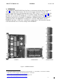
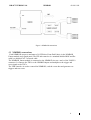
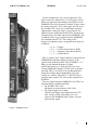
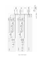
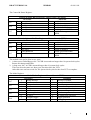
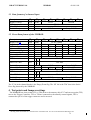
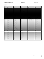
NIK HEF
NATIONAL INSTITUTE FOR NUCLEAR AND HIGH ENERGY PHYSICS
ETR 99-06
NIMROD,
16 channel read out
driver for the Drift
Chambers used in the
L3+Cosmics project.
September 1999
Project no.: 32010
H.L.Groenstege
P.A.M. Rewiersma
T.A.M. Wijnen
A.N.M. Zwart
email: albert@nikhef.nl
The NIKHEF MDT read out driver is
a VME module that collects data from
the TDCs, connected to the Drift
Chambers. The data from several MDT
chambers is merged and can be read by
a VME master
Check for most recent version:
http://www.nikhef.nl/pub/departments/et/L3/cosmics
NIKHEF, DEPARTMENT OF
ELECTRONIC TECHNOLOGY
P.O.box 41882, NL 1009 DB AMSTERDAM
DRAFT VERSION 1.0
NIMROD
09-09-1999
Table of contents
1.
1.1
NIMROD
NIMROD connections
3
4
2.1
2.2
2.3
2.4
General description
Block diagram
Frontend FIFO
Event memory
VME Interface
7
7
7
8
8
3.1
3.2
Data format
Data format of a channel input
Event Data format of the NIMROD
10
11
11
4.
Connector pinout
11
5.
Abbreviations
15
2.
3.
Figures
Figure 1: NIMROD modules
Figure 2: NIMROD connections
Figure 3: NIMROD front
Figure 4: Block Diagram
Figure 5: Base address
3
4
5
6
8
2
DRAFT VERSION 1.0
NIMROD
09-09-1999
1. NIMROD
The NIMROD (NIKHEF MDT Read Out Driver) concentrates the data from a number of
TDCs1 into a single output register. The unit receives trigger and clock from the CTP
(Central Trigger Processor) and distributes this to the TDCs. In the L3 + Cosmics project the
function of the CTP is fulfilled by the CTT-V2 (Cosmics Trigger and Timing module)2 and
the TDCs are interfaced to the NIMROD on a CPC (Cosmics Personality Card)3. A complete
NIMROD consists of a set of modules; a NIMROD, a NIMROD_fanout module and four
patchpanel boards. The NIMROD is a standard 6U * 160 mm VME module. Several
NIMRODs may share a VME crate, controlled by a single master. This controller reads the
event data and takes care of various settings in the NIMRODs.
Figure 1: NIMROD modules
1
A 24 channel TDC for the ATLAS precision muon chambers, Y. Arai (KEK) J. Christiansen (CERN).
ETR 99-01: Cosmics Trigger and Timing Module, H. Verkooyen
//www.nikhef.nl/pub/departments/et/L3/cosmics/.
3
ETR 99-02: Cosmics Personality Card, H Groenstege et all
//www.nikhef.nl/pub/departments/et/L3/cosmics/
2
3
DRAFT VERSION 1.0
NIMROD
09-09-1999
Figure 2: NIMROD connections
1.1 NIMROD connections
Each NIMROD accepts a maximum of 16 FELinks (Front-End Links) via the NIMROD_
Fanout module and a patch panel. The FELink connector is a standard shielded RJ45 and the
cable is a shielded CAT 5 network cable.
The NIMROD_fanout module is connected to the NIMROD via row a and c of the VME P2
connector. It connects the TDCs to the NIMROD inputs and multiplexes the trigger and
reset signals to the TDCs.
The VME interface is used to control the NIMROD, read the event data and generate test
triggers and test resets.
4
DRAFT VERSION 1.0
NIMROD
09-09-1999
On the frontpanel are two 10-pin connectors. The
upper connector, labeled Test, is a JTAG port used to
perform in system programming of the FPGAs on the
NIMROD. The lower connector, labeled Trigger, must
be connected to the CTP via the trigger bus to receive
the 40 MHz TDC clock, the coded trigger and reset
signals and to return the inhibit trigger signal. The
signal levels are differential Positive ECL and must be
terminated with 100 Ohm after the last NIMROD. The
combined inhibit trigger signals from the NIMRODs
are terminated in the CTP. The coding of the
trigger/reset signals on three sequential clock pulses is
as follows:
1, 0, 0 = >Trigger
1, 0, 1 = > Event Counter Reset (ECR)
1, 1, 0 = > Bunch Counter Reset (BCR)
1, 1, 1 = > Global Reset
Due to coding of the Trigger and Reset internal in the
NIMROD the maximum trigger frequency is the
system clock divided by three. This is 20MHz/3 = 6.7
MHz (so the minimal deadtime is 150ns) .
All FELink signals to or from the TDCs are Low
Voltage Differential Signals (LVDS). The serial data
from the TDCs is received via two differential lines
using DS coding without handshaking. The data
consist of a startbit, followed by 32 bit TDC data, a
paritybit and a stopbit. The rate on this connection is
40 Mbit/s.
The two signals from the NIMROD to the TDCs are
also distributed via differential lines:
• The 40 MHz TDC clock.
All signals are synchronous to this clock.
• The coded trigger/reset signal.
Which is the trigger/reset signal from the CTP
after a delay of four clock pulses. For test
purposes the NIMROD mode register can also
generate this signal.
Figure 3: NIMROD front
5
Figure 4: Block Diagram
DRAFT VERSION 1.0
NIMROD
09-09-1999
2. General description
2.1 Block diagram
The trigger and reset from the CTP is decoded in the Trigger and Reset Decoder. The coded signals
are distributed to the TDCs via the FELinks. The Global Reset is used internally to reset all counters
and FIFOs in the NIMROD; the Event Counter Reset only clears the Event Counter in the Header
block and the Bunch Counter Reset is not used in the NIMROD.
On a trigger, the Event Counter in the Header block is incremented and the data is stored in a circular
buffer in the Event Memory. The address is stored in the Look Up Table (LUT) to be used for read out.
Then, if the header enable bit is set, a flag header word (0x18100000) is stored, hereafter the flags are
read and stored on the next addresses. When the circular buffer or the LUT is full, writing is inhibited
and the triggers are stored in the Frontend FIFO.
Simultaneously the TDCs will sent data via the FELinks to the NIMROD. This data is converted from
serial to parallel (32 bit) and stored into a FIFO. The data is read from the FIFO. If it is a leader of an
event (Begin Of Group), the start address of the event is stored in the LUT. On the next address the
Begin Of Group word is stored in the memory, followed by the next word from the FIFO until the
trailer of the event (End Of Group) is detected. Then the Channel Header word is stored in the memory
on the begin address of the event. When there is no data between the Begin Of Group (BOG) and End
Of Group (EOG), the Event Empty bit is set in the Channel Header. After the writing of the Channel
Header the event-present counter is incremented. If the event-present counter is not equal to zero, the
event present flag of this channel is asserted.
When all channels have an event present, the Read-Out block starts a read-out cycle. At this point the
Header block and the enabled channels get the read addresses from the LUTs, the Header block reads
the Begin Of Event from the memory and puts it in the Output Register in the VME interface. Then
Read-Out waits for the VME Master to read the output register before it enables the Header block to
get the next word. If the Header block has read the data of the event it decrements its event-present
counter and enables the first enabled channel to read the data until the read address is equal to the next
address in the LUT or equal to the write address. Then the channel decrements its event counter and
enables the next channel to send its data. This continues until all channels have read the event data from
the memory. The Read-Out now terminates the read-out cycle and writes the End Of Event in the
Output Register. If the Read-Out detects an Empty Event bit in a Channel Header, it will skip this
channel, thus performing a zero-suppressed read-out. This zero-suppress is bypassed on event 1
modulo 0x1000 events. The data rate of the Read-Out via VME is 6 MB/sec (670 ns/word).
2.2 Shift Register
The serial data from the TDCs with LSB first is shifted in this register, if the last bit (MSB) is shifted
in, the parity is checked. When the parity is not correct, the Serial Error Flag is asserted and the Serial
Error bit (bit 26) is set in the TDC data. Then the data is loaded in the Frontend FIFO.
The serial error flag will be cleared when the flag word is written in the Event memory.
2.3 Frontend FIFO
The data in the event memory is written by 18 sources (16 Channels, the Header and the VME
interface). These sources are scheduled with the system clock. Therefore a 64 words deep Frontend
FIFO is implemented for every channel to store the data which is not yet written in the Event Memory.
To prevent the FIFO to overrun an inhibit trigger is generated when the FIFO is half full (32 words).
The inhibit trigger is released when the FIFO is empty. The input rate of the shift register is 35 bits @
40 MHz. This results in an input rate of the FIFO of 1.14 MHz (875 ns) per word. With a system clock
of 20 MHz the output rate is1.11 MHz (20 divided by 18), which is almost the same as the input rate.
7
DRAFT VERSION 1.0
NIMROD
09-09-1999
So the FIFO will only be filled when the write to memory is inhibited by a memory full or a LUT full
condition.
The system clock of the first version NIMROD was 7.5 MHz., So the output rate of the FIFO was 0.41 MHz. (2.44 µs)
which is much lower than the input rate. Therefor a mechanism is built in that when the FIFO is almost full (56 words)
only the Begin Of Group and End Of Group words are stored in the FIFO. This to prevent corruption of the bookkeeping
of the event fragments.
2.4 Event memory
The event memory is a synchronous ZBT RAM that does not need the deselect cycle between a write
and a read cycle. The memory clock is 40MHz; this enables a write and a read during one system clock
cycle.
The memory has 17 circular buffers of 2K 32-bit words, one for every Channel plus the Header. For
debugging purposes the memory is accessible from VME, the address map is given in the next chapter.
2.5 VME Interface
The VME Interface is compliant to VME64x and all devices can be accessed in the A24D32 and
A32D32 addressing modes. The base address is defined by the Geographical Address pins on the
backplane connector. In case the backplane does not support geographical addressing, jumpers J54 (=
Ga0) to J50 (= Ga4) should be installed to define the base address of the NIMROD. If no jumpers are
installed and no geographical addressing is supported, the default value of Ga(4:0) = 0x4.
Figure 5: Base address
Valid Address Modifier codes are 0x09 and 0x0D for A24D32 transfers, 0x39 and 0x3D for A24D32
transfers and 0x2F for accessing of the Configuration ROM (CR) and Control & Status Register
(CSR).
The Configuration ROM is a 64 x 8 bit ROM that contains module identification data. The ROM
addresses are mapped in the VME address space from address offset 0x03 to 0xFF on every fourth
byte.
8
DRAFT VERSION 1.0
NIMROD
09-09-1999
The Control & Status Register:
Bit 7
Bit 4
Bit 3
Bit 7
Bit 4
Bit 3
1
0
1
0
1
0
Control & Status Bit Set Register, address offset = 0x7FFFB
On Writes
On Reads
put module in reset mode
1
module is in reset mode
no effect
0
module is not in reset mode
enable module
1
module is enabled
no effect
0
module is disabled
no effect
1
module generated BERR
no effect
0
module did not generate
BERR
Control & Status Bit Clear Register, address offset = 0x7FFFC
On Writes
On Reads
1
remove module from reset mode
1
module is in reset mode
0
no effect
0
module is not in reset mode
1
disable module
1
module is enabled
0
no effect
0
module is disabled
1
clear BERR bit
1
module generated BERR
0
no effect
0
module did not generate
BERR
The module reset can be done in two ways:
1. A short reset; Global Reset or bit 7 in CSR is asserted not longer then 16 system clock cycles.
Resets all counters and FIFOs
2. A long reset; bit 7 in CSR is asserted longer then 16 system clock cycles.
This reset does the same as a short reset, but also clears the LUTs.
After this reset one has to wait for 786 system clock cycles for the clear LUT to complete.
The Mode Register:
Bit 7
Bit 3
Bit 2
Bit 1
Bit 0
1
0
1
0
1
0
1
0
1
0
Mode Bit Set Register address offset = 0x7FFF3
On Writes
On Reads
enable interrupt
1
interrupt is enabled
no effect
0
interrupt is disabled
Generate bunch reset
1
bunch reset generated
no effect
0
no bunch reset generated
Generate event reset
1
event reset generated
no effect
0
no event reset generated
Generate global reset
1
global reset generated
no effect
0
no global reset generated
Generate trigger
1
trigger generated
no effect
0
no trigger generated
9
DRAFT VERSION 1.0
1
0
1
0
1
0
1
0
1
0
Bit 7
Bit 3
Bit 2
Bit 1
Bit 0
NIMROD
09-09-1999
Mode Bit Clear Register address offset = 0x7FFEF
On Writes
On Reads
Disable interrupt
1
interrupt is enabled
no effect
0
interrupt is disabled
clear bunch reset bit
1
bunch reset generated
no effect
0
no bunch reset generated
clear event reset bit
1
event reset generated
no effect
0
no event reset generated
clear global reset bit
1
global reset generated
no effect
0
no global reset generated
clear trigger bit
1
trigger generated
no effect
0
no trigger generated
The Event Memory has an address offset of 0x40000. On this address the 8KB cyclic buffer of
channel 0 starts, channel 1 starts at 0x42000 etc… until the buffer of the header that starts at 0x60000.
The Flags words are read-only and the address offsets are:
0x200
0x204
0x208
0x20C
event present
inhibit
LUT full
memory full
0x210
0x214
0x218
0x21C
FIFO empty
FIFO half full
channel enable
serial error
Except for the channel enable, the flags are read-only. Bit 16 of the flag words is the header flag, bit
15 to 0 are the flags of channel 15 to 0. Reading of the flags should not be done when the trigger is
enabled, this corrupts the flag words in the event data.
The readout register is mapped to multiple addresses to enable block- or DMA transfers; the address
offset is 0x300 to 0x1000. Reading the readout register when there is no event present will return 0x0.
The interrupter is of a single level type. An interrupt is generated when the interrupt enable is set in
the mode register and the event present flags of all enabled channels are set. The interrupt request level
is set in the interrupt request register at address offset 0x110. If bit 1 is set, the interrupt level is 1, if bit
2 is set, the interrupt level is 2, and so on until bit 7 then the interrupt level is 7 (bit 0 is not used). Only
one bit must be set in the interrupt request level register. After reset the default interrupt request level is
2. The interrupt vector is set in the interrupt vector register at address offset 0x114.
3. Data format
The description below gives a summary of the data format that the NIMROD uses. The data format is
compliant to the L3 Cosmics data format4. It should be noted that the NIMROD only tests on BOG and
EOG for administration purposes and that all incoming data appears in the event data.
4
KUN internal note, HEN425, The L3+Cosmics Data format, Thei Wijnen et all
//www.hef.kun.nl/l3c/
10
DRAFT VERSION 1.0
NIMROD
09-09-1999
3.1 Data format of a channel input
Description
Bit
31 - 28
Bit
27 - 24
Begin Of Group
TDC data
More TDC data
End Of Group
1010
0011
0011
1101
0100
Bit
23 - 20
Bit
19 - 16
Bit
15 - 12
Bit
11 - 8
ECNT
Bit
7 - 4
Bit
3 - 0
Card ID
TDC data
TDC data
0101
ECNT
Group WCNT
3.2 Event Data format of the NIMROD
Description
Bit
31 - 28
Bit
27 - 24
Begin Of Event
Flag Header*
LUT full flags*
Memory full flags*
FIFO half full flags*
Serial error flags*
Channel Header
Begin Of Group
TDC data
1000
0001
0001
0001
0001
0001
0001
1010
0011
0000
1000
1001
1001
1001
1001
1000
0100
More TDC data
0011
End Of Group
Channel Header
Begin Of Group
TDC data
1101
0001
1010
0011
More TDC data
0011
End Of Group
End Of Event
1101
1111
Bit
23 - 20
0000
0000
0001
0010
0011
0001
S
E
S
E
0101
1000
0100
Bit
19 - 16
Bit
15 - 12
Bit
11 - 8
Bit
7 - 4
ECNT (24bits)
0000
0000
0000
0000
000x
xxxx
xxxx
xxxx
000x
xxxx
xxxx
xxxx
000x
xxxx
xxxx
xxxx
000x
xxxx
xxxx
xxxx
000E
0000
Channel ID
ECNT
Card ID
TDC data
Bit
3 - 0
0000
xxxx
xxxx
xxxx
xxxx
TDC data
0000
S
E
S
E
0101
ECNT
000e
ECNT
0000
Group WCNT
Channel ID
Card ID
TDC data
TDC data
ECNT
Event WCNT
Group WCNT
The ‘E’ bit in the channel header is the Empty Event flag. The ‘SE’ bit in the TDC data is the Serial
Error flag detected by the NIMROD.
4. Test points and Jumpers settings
The NIMROD has 4 test points (TP1 to TP4) next to the memory chip IC17 and one test point (TP5)
next to the Trigger Connector. TP1 to TP4 are connected to the memory control signals, TP5 is
connected to pin 10 of the trigger connector and is not used.
*
The flag words and header are inserted in the event data if bit 16 is set in the channel enable flag word.
11
DRAFT VERSION 1.0
TP1
TP2
TP3
TP4
TP5
NIMROD
09-09-1999
Memory Chip Select
Memory Clock
Write Enable
Output Enable
not used
The user definable jumpers are the address jumpers (J50 to J55) and the 3V3 power select jumper
(J5). If J5 pos. 1 is connected, the 3V3 power is obtained from the backplane, if pos 2 is connected, the
3V3 is coming from the on board power regulator. When the NIMROD is connected to a VME64x
compatible backplane, all the address jumpers should be removed and J5 can be either in pos 1 or 2. In
all other cases the address jumpers should be installed and J5 pos. 2 connected.
5. Connector pinout
Trigger
Pin
10
8
6
4
2
Signal
NC
Trigger/Reset (-)
GND
Clock (-)
GND
Pin
9
7
5
3
1
Signal
GND
Trigger/Reset (+)
GND
Clock (+)
Trigger Disable
Test
Pin
10
8
6
4
2
Signal
NC
GND
+5V
GND
NC
Pin
9
7
5
3
1
Signal
NC
TDO
TDI
TMS
TCK
Channel input
Pin
Signal
1
Clock(+)
2
Clock(-)
3
Trigger/Reset(+)
4
Data(-)
5
Data(+)
6
Trigger/Reset(-)
7
Strobe(+)
8
Strobe(-)
9
GND
10
GND
12
DRAFT VERSION 1.0
VME P1
Pin
Row z
1
NC
2
GND
3
NC
4
GND
5
NC
6
GND
7
NC
8
GND
9
NC
10
GND
11
NC
12
GND
13
NC
14
GND
15
NC
16
GND
17
NC
18
GND
19
NC
20
GND
21
NC
22
GND
23
NC
24
GND
25
NC
26
GND
27
NC
28
GND
29
NC
30
GND
31
NC
32
GND
NIMROD
Row a
D0
D1
D2
D3
D4
D5
D6
D7
GND
NC
GND
DS1_N
DS0_N
WRITE_N
GND
DTACK_N
GND
AS_N
GND
IACK_N
IACKIN_N
IACKOUT_N
AM4
A7
A6
A5
A4
A3
A2
A1
NC
+5V
Row b
NC
NC
NC
BG0IN_N
BG0OUT_N
BG1IN_N
BG1OUT_N
BG2IN_N
BG2OUT_N
BG3IN_N
BG3OUT_N
NC
NC
NC
NC
AM0
AM1
AM2
AM3
GND
NC
NC
GND
IRQ7_N
IRQ6_N
IRQ5_N
IRQ4_N
IRQ3_N
IRQ2_N
IRQ1_N
NC
+5V
09-09-1999
Row c
D8
D9
D10
D11
D12
D13
D14
D15
GND
NC
BERR_N
SYS_RES_N
LWORD_N
AM5
A23
A22
A21
A20
A19
A18
A17
A16
A15
A14
A13
A12
A11
A10
A9
A8
NC
+5V
Row d
NC
NC
NC
NC
NC
NC
NC
NC
GAP_N
GA0_N
GA1_N
3V3
GA2_N
3V3
GA3_N
3V3
GA4_N
3V3
NC
3V3
NC
3V3
NC
3V3
NC
3V3
NC
3V3
NC
3V3
NC
NC
13
DRAFT VERSION 1.0
VME P2
Pin
Row z
1
NC
2
GND
3
NC
4
GND
5
NC
6
GND
7
NC
8
GND
9
NC
10
GND
11
NC
12
GND
13
NC
14
GND
15
NC
16
GND
17
NC
18
GND
19
NC
20
GND
21
NC
22
GND
23
NC
24
GND
25
NC
26
GND
27
NC
28
GND
29
NC
30
GND
31
NC
32
GND
NIMROD
Row a
GND
SER_DATA0
SER_DATA1
GND
SER_DATA2
SER_DATA3
GND
SER_DATA4
SER_DATA5
GND
SER_DATA6
SER_DATA7
GND
SER_DATA8
SER_DATA9
GND
SER_DATAA
SER_DATAB
GND
SER_DATAC
SER_DATAD
GND
SER_DATAE
SER_DATAF
GND
GND
GND
GND
GND
CPCTRST
NC
NC
Row b
+5V
GND
NC
A24
A25
A26
A27
A28
A29
A30
A31
GND
+5V
D16
D17
D18
D19
D20
D21
D22
D23
GND
D24
D25
D26
D27
D28
D29
D30
D31
GND
+5V
09-09-1999
Row c
GND
SER_STRB0
SER_STRB1
GND
SER_STRB2
SER_STRB3
GND
SER_STRB4
SER_STRB5
GND
SER_STRB6
SER_STRB7
GND
SER_STRB8
SER_STRB9
GND
SER_STRBA
SER_STRBB
GND
SER_STRBC
SER_STRBD
GND
SER_STRBE
SER_STRBF
GND
GND
GND
GND
GND
CPCTRCLK
NC
NC
Row d
NC
NC
NC
NC
NC
NC
NC
NC
NC
NC
NC
NC
NC
NC
NC
NC
NC
NC
NC
NC
NC
NC
NC
NC
NC
NC
NC
NC
NC
NV
NC
NC
14
DRAFT VERSION 1.0
NIMROD
09-09-1999
6. Abbreviations
Abbreviations and other less well known definitions used in this (and other) documents.
BCID
BCR
CPC
CTP
CTT
ECR
FELink
JTAG
LVDS
LUT
Bunch Crossing IDentifier. Reset by BCR.
Bunch Counter Reset, used to synchronize Front-End electronics.
Cosmics Personality Card. Contains TDCs and interface logic
Central Trigger Processor. Generates first level trigger.
Cosmics Trigger and Timing module.
Event Counter Reset.
Front-End Link. Carries the Reset/Trigger signals to the TDC and
transports the TDC data to the NIMROD.
Joint Test Action Group IEEE 1149.1. Functional test and
programming facility.
Low Voltage Differential Signaling. ±400 mV. Compatible with 3V
and 5V supply voltages.
Look Up Table, contains start addresses of events in memory.
15