1
INTERFACING TOUCH SCREEN
WITH FPGA
SUBMITTED TO:
INNOVATION CELL, INDIAN INSTITUTE OF
TECHNOLOGY, BOMBAY
SUBMITTED BY:
AEISHWARYA BAVISKAR
ELECTRICAL AND ELECTRONICS ENGINEERING, VNIT NAGPUR
JENIL SAVLA
ELECTRICAL AND ELECTRONICS ENGINEERING, VNIT NAGPUR
ACKNOWLEDGEMENT:
We would like to thanks Prof. R. K. Singh and Prof. S. N. Merchant
for giving us
opportunity for this project.
We would like to extend our sincere thanks to EbrahimAttarwala for
his
Guidance and support in completion of this project.
We would like to express my deepest appreciation to all those who
provided me the possibility to complete this project.
We are highly indebted to innovation cell IIT, Bombay for their
guidance and constant supervision as well as for providing necessary
information regarding the project & also for their support in
completing the project.
Index:
1.
2.
3.
4.
5.
6.
7.
8.
9.
INTRODUCTION
WHAT IS FPGA?
DE2I-150 BOARD
QUARTUS II
GETTING STARTED WITH FPGA
EXPERIMENTAL SETUP
TOUCH SCREEN
SPI SERIAL INTERFACE
CODE
INTRODUCTION
THE MAIN GOAL OF THIS PROJECT IS TO INTERFACE A TOUCH
SCREEN WITH THE FPGA. A RESISTIVE FOUR WIRE TOUCH
SCREEN IS USED FOR THE SAME. TEXAS INSTRUMENT’S ADS7843
SERVES AS A TOUCH SCREEN CONTROLLER WHICH CONVERTS
ANALOG SIGNALS FROM TOUCH SCREEN TO DIGITAL SIGNAL
THAT LATER IS PROVIDED AS AN INPUT TO THE FPGA.
PROGRAMMING OF THE FPGA IS DONE IN VERILOG HDL
LANGUAGE. THE BOARD IS PROVIDED WITH AN INDEPENDENT
PROGRAMMING PLATFORM QUARTUS II.
THE SERIAL COMMUNICATION IS ESTABLISHED BETWEEN THE
FPGA AND THE ADC USING SPI SERIAL BUS INTERFACE.
WHAT IS AN FPGA?
Field Programmable Gate Arrays (FPGAs) are semiconductor devices that are based around a matrix of
configurable logic blocks (CLBs) connected via programmable interconnects. FPGAs can be
reprogrammed to desired application or functionality requirements after manufacturing.
Basic elements of FPGA:
> Configurable logic blocks (CLBs)
> Configurable input output blocks
> Two layer metal network of vertical and horizontal lines for interconnecting the CLBs and FPGAs
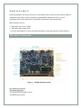
THE DE2I-150 BOARD:
FPGA SPECIFICATIONS:
FEATURED DEVICES
Cyclone IV EP4CGX150DF31 device
720 M9K memory blocks
6,480 Kbits embedded memory
FPGA CONFIGURATION
JTAG and AS mode configuration
EPCS64 serial configuration device
On-board USB Blaster circuitry
MEMORY DEVICES
128MB (32Mx32bit) SDRAM
4MB (1Mx32) SSRAM
64MB (4Mx16) Flash with 16-bit mode
CONNECTORS
Ethernet 10/100/1000 Mbps ports
High Speed Mezzanine Card (HSMC)
40-pin expansion port
VGA-out connector
VGA DAC (high speed triple DACs)
DB9 serial connector for RS-232 port with flow control
CLOCK
Three 50MHz oscillator clock inputs
DISPLAY
16x2 LCD module
18 slide switches and 4 push-buttons switches
18 red and 9 green LEDs
Eight 7-segment displays
QUARTUS II
Quartus II is a software tool produced by Altera for analysis and synthesis of HDL designs, which
enables the developer to compile their designs, perform timing analysis, examine RTL diagrams,
simulate a design's reaction to different stimuli, and configure the target device with the programmer.
Its features include:
An implementation of VHDL and Verilog for hardware description.
Visual edition of logic circuits.
Vector waveform simulation.
We have used Quartus II 12.1 and coding is done in Verilog. To start working on your fpga refer
the user manual and the getting started guide which helps through the initial steps in quartus II.
Verilog tutorials: www.hdlexpress.com- by Kirk Weedman.
Books referred: Verilog HDL programming by Samir
Palnitkar.http://d1.amobbs.com/bbs_upload782111/files_33/ourdev_585395BQ8J9A.pdf
You can start with some basic codes once a project is made in quartus.
http://www.terasic.com.tw/cgi-bin/page/archive.pl?Language=English&No=529
GETTING STARTED WITH THE FPGA
IMPLEMENTING LOGIC GATES ON FPGA(USING BLOCK DIAGRAM FILE):
A block diagram file is an easy way to get started. Various logic gates and simple ICs such as encoders, multiplexers
are available ready to use in the library. Here is an implementation of NAND gate:
https://www.youtube.com/watch?v=auQ7wpVH-0Q
BINARY UP-COUNTER USING ON BOARD LEDS AND PUSH BUTTONS:
There are 18 red and 7 green leds mounted on the board along with four push buttons and 18 slider switches. Here
is a code to access some of the leds and push buttons.
module countertest(KEY,LEDR);
input[1:0] KEY;
output[7:0] LEDR;
counter counter1(KEY[0],KEY[1],LEDR[7:0]);
endmodule
module counter (C,CLR,Q);
input C,CLR;
output [7:0] Q;
reg[7:0] tmp;
always @(posedge C or posedge CLR)
begin
if(CLR)
tmp = 8'b00000000;
else
tmp = tmp + 8'b00000001;
end
assign Q = tmp;
endmodule
ACCESSING INTERNAL CLOCK TO BLINK ONBOARD LEDS:
module clock_test (CLOCK_50, LEDR);
input CLOCK_50 ;
output [17:0] LEDR;
reg [17:0] tmp;
always @(posedge CLOCK_50)
begin
tmp <= tmp + 1'b1;// increment counter
end
assign LEDR = tmp;
endmodule
USING THE GPIO PINS TO MAKE AND GATE:
module andgate(input_1,input_2,GPIO);
input input_1;
input input_2;
output [0:0]GPIO;
wire and_temp;
assign and_temp = input_1 & input_2;
assign GPIO[0] = and_temp;
endmodule
SERIAL COMMUNICATION IN FPGA:
USART SERIAL receiver:
module async_receiver(
input clk,
input RxD,
output reg RxD_data_ready = 0,
output reg [7:0] RxD_data = 0,
// data received, valid only (for one clock cycle) when RxD_data_ready is asserted
// We also detect if a gap occurs in the received stream of characters
// That can be useful if multiple characters are sent in burst
// so that multiple characters can be treated as a "packet"output RxD_idle,
// asserted when no data has been received for a while output reg RxD_endofpacket = 0
// asserted for one clock cycle when a packet has been detected (i.e. RxD_idle is going high)
);
parameter ClkFrequency = 25000000; // 25MHz
parameter Baud = 115200;
parameter Oversampling = 8; // needs to be a power of 2
// we oversample the RxD line at a fixed rate to capture each RxD data bit at the "right" time
// 8 times oversampling by default, use 16 for higher quality reception generate
if(ClkFrequency<Baud*Oversampling) ASSERTION_ERROR PARAMETER_OUT_OF_RANGE("Frequency too
low for current Baud rate and oversampling");
if(Oversampling<8 || ((Oversampling & (Oversampling-1))!=0)) ASSERTION_ERROR
PARAMETER_OUT_OF_RANGE("Invalid oversampling value");
endgenerate
reg [3:0] RxD_state = 0;
`ifdef SIMULATION
wire RxD_bit = RxD;
wire sampleNow = 1'b1; // receive one bit per clock cycle
`else
wire OversamplingTick;
BaudTickGen #(ClkFrequency, Baud, Oversampling) tickgen(.clk(clk), .enable(1'b1), .tick(OversamplingTick));
// synchronize RxD to our clk domain
reg [1:0] RxD_sync = 2'b11;
always @(posedge clk) if(OversamplingTick) RxD_sync <= {RxD_sync[0], RxD};
// and filter it
reg [1:0] Filter_cnt = 2'b11;
reg RxD_bit = 1'b1;
always @(posedge clk)
if(OversamplingTick)
begin
if(RxD_sync[1]==1'b1 && Filter_cnt!=2'b11) Filter_cnt <= Filter_cnt + 1'd1;
else
if(RxD_sync[1]==1'b0 && Filter_cnt!=2'b00) Filter_cnt <= Filter_cnt - 1'd1;
if(Filter_cnt==2'b11) RxD_bit <= 1'b1;
else
if(Filter_cnt==2'b00) RxD_bit <= 1'b0;
end
// and decide when is the good time to sample the RxD line
function integer log2(input integer v); begin log2=0; while(v>>log2) log2=log2+1; end endfunction
localparam l2o = log2(Oversampling);
reg [l2o-2:0] OversamplingCnt = 0;
always @(posedge clk) if(OversamplingTick) OversamplingCnt <= (RxD_state==0) ? 1'd0 : OversamplingCnt + 1'd1;
wire sampleNow = OversamplingTick && (OversamplingCnt==Oversampling/2-1);
`endif
// now we can accumulate the RxD bits in a shift-register
always @(posedge clk)
case(RxD_state)
4'b0000: if(~RxD_bit) RxD_state <= `ifdef SIMULATION 4'b1000 `else 4'b0001 `endif; // start bit found?
4'b0001: if(sampleNow) RxD_state <= 4'b1000; // sync start bit to sampleNow
4'b1000: if(sampleNow) RxD_state <= 4'b1001; // bit 0
4'b1001: if(sampleNow) RxD_state <= 4'b1010; // bit 1
4'b1010: if(sampleNow) RxD_state <= 4'b1011; // bit 2
4'b1011: if(sampleNow) RxD_state <= 4'b1100; // bit 3
4'b1100: if(sampleNow) RxD_state <= 4'b1101; // bit 4
4'b1101: if(sampleNow) RxD_state <= 4'b1110; // bit 5
4'b1110: if(sampleNow) RxD_state <= 4'b1111; // bit 6
4'b1111: if(sampleNow) RxD_state <= 4'b0010; // bit 7
4'b0010: if(sampleNow) RxD_state <= 4'b0000; // stop bit
default: RxD_state <= 4'b0000;
endcase
always @(posedge clk)
if(sampleNow && RxD_state[3]) RxD_data <= {RxD_bit, RxD_data[7:1]};
//reg RxD_data_error = 0;
always @(posedge clk)
begin
RxD_data_ready <= (sampleNow && RxD_state==4'b0010 && RxD_bit); // make sure a stop bit is
received
//RxD_data_error <= (sampleNow && RxD_state==4'b0010 && ~RxD_bit); // error if a stop bit is not
received
end
reg [l2o+1:0] GapCnt = 0;
always @(posedge clk) if (RxD_state!=0) GapCnt<=0; else if(OversamplingTick & ~GapCnt[log2(Oversampling)+1])
GapCnt <= GapCnt + 1'h1;
assign RxD_idle = GapCnt[l2o+1];
always @(posedge clk) RxD_endofpacket <= OversamplingTick & ~GapCnt[l2o+1] &&GapCnt[l2o:0];
endmodule
USART SERIAL TRANSMITTER:
// Serial port demo program
// Assumptions: 50Mhz clock rate
module serial( data, clk, ser,start);
input clk;
output ser;
input [7:0]data;
// Start signal tells it to start sending bits
input start;
//The bits of data to send
//reg [7:0] data;
/////////////////////////////////////////////////////////////////////////////
// Serial port clock generator
// Generate a 9600 baud clock signal for the serial port by dividing the
// 50Mhz clock by 5208
reg [14:0] clockdiv;
// Count from 0..5207 then reset back to zero
always @(posedge clk)
begin
if (clockdiv == 434)
clockdiv <= 0;
else
clockdiv <= clockdiv + 1;
end
// The serclock is a short pulse each time we are reset
wire serclock = (clockdiv == 0);
/////////////////////////////////////////////////////////////////////////////
// Serial port state machine
// Only start the state machine when "start" is set. Only advance to the
// next state when serclock is set.
reg [3:0] state;
always @(posedge clk)
begin
case (state)
4'b0000: if (start) state <= 4'b0001;
4'b0001: if (serclock) state <= 4'b0010; // Start bit
4'b0010: if (serclock) state <= 4'b0011; // Bit 0
4'b0011: if (serclock) state <= 4'b0100; // Bit 1
4'b0100: if (serclock) state <= 4'b0101; // Bit 2
4'b0101: if (serclock) state <= 4'b0110; // Bit 3
4'b0110: if (serclock) state <= 4'b0111; // Bit 4
4'b0111: if (serclock) state <= 4'b1000; // Bit 5
4'b1000: if (serclock) state <= 4'b1001; // Bit 6
4'b1001: if (serclock) state <= 4'b1010; // Bit 7
4'b1010: if (serclock) state <= 4'b1111; // Stop bit
default: state <= 4'b0000;
// Undefined, skip to stop
endcase
end
///////////////////////////////////////////////////////////////////////////////
// Serial port data
// Ensure that the serial port has the correct data on it in each state
reg outbit;
always @(posedge clk)
begin
case (state)
4'b0000: outbit <= 1;
// idle
4'b0001: outbit <= 0;
// Start bit
4'b0010: outbit <= data[0];
// Bit 0
4'b0011: outbit <= data[1];
// Bit 1
4'b0100: outbit <= data[2];
// Bit 2
4'b0101: outbit <= data[3];
// Bit 3
4'b0110: outbit <= data[4];
// Bit 4
4'b0111: outbit <= data[5];
// Bit 5
4'b1000: outbit <= data[6];
// Bit 6
4'b1001: outbit <= data[7];
// Bit 7
4'b1010: outbit <= 1;
// Stop bit
default: outbit <= 1;
// Bad state output idle
endcase
end
// Output register to pin
assign ser = outbit;
///////////////////////////////////////////////////////////////////////////////
// Test by outputting a letter 'd'
always @(posedge clk)
begin
start = 1;
end
endmodule
UART BAUD RATE GENERATOR
module BaudTickGen(input clk, enable,output tick ); // generate a tick at the specified baud rate * oversampling
parameter ClkFrequency = 25000000;
parameter Baud = 115200;
parameter Oversampling = 1;
function integer log2(input integer v); begin log2=0; while(v>>log2) log2=log2+1; end endfunction
localparam AccWidth = log2(ClkFrequency/Baud)+8; // +/- 2% max timing error over a byte
reg [AccWidth:0] Acc = 0;
localparam ShiftLimiter = log2(Baud*Oversampling >> (31-AccWidth)); // this makes sure Inc calculation doesn't
overflow
localparam Inc = ((Baud*Oversampling << (AccWidthShiftLimiter))+(ClkFrequency>>(ShiftLimiter+1)))/(ClkFrequency>>ShiftLimiter);
always @(posedge clk) if(enable) Acc <= Acc[AccWidth-1:0] + Inc[AccWidth:0]; else Acc <= Inc[AccWidth:0];
assign tick = Acc[AccWidth];
endmodule
The above three modules are basic modules for serial communication. Then you can write your own code to
perform serial communication as you want. For example for swapping the given stream of serial bytes, below is a
code:
module processor(clk, rxReady, rxData, txBusy, txStart, txData);
input clk;
input[7:0] rxData;
input rxReady;
input txBusy;
output reg txStart;
output reg[7:0] txData;
localparam READ=0, SOLVING=1, WRITE1=2, WRITE2=3;
localparam LEN = 10;
localparam LENMAX = LEN - 1;
integer ioCount;
reg[7:0] data[0:LENMAX];
integer state;
initial begin
txStart = 0;
state = READ;
end
always @(posedge clk) begin
case (state)
READ: begin
if (rxReady) begin
data[ioCount] = rxData;
if (ioCount == LENMAX) begin
ioCount = 0;
state = SOLVING;
end else begin
ioCount = ioCount + 1;
end
end
end
SOLVING: begin
integer i;
for (i = 0; i < LEN/2; i = i + 1) begin
reg[7:0] swap;
swap = data[i];
data[i] = data[LENMAX-i];
data[LENMAX-i] = swap;
end
state = WRITE1;
end
WRITE1: begin
if (!txBusy) begin
txData = data[ioCount];
txStart = 1;
state = WRITE2;
end
end
WRITE2: begin
txStart = 0;
if (ioCount != LENMAX) begin
ioCount = ioCount + 1;
state = WRITE1;
end else begin
ioCount = 0;
state = READ;
end
end
endcase
end
endmodule
For more reference:
- http://www.fpga4fun.com/SerialInterface.html
- http://www.sparxeng.com/blog/software/talking-rs-232-with-cyclone-ii-fpga-part-1
- http://www.sparxeng.com/blog/software/talking-rs-232-with-cyclone-ii-fpga-part-2
- http://www.sparxeng.com/blog/software/communicating-with-your-cyclone-ii-fpga-over-serial-port-part-3-numbercrunching
EXPERIMENTAL SETUP
RESISTIVE TOUCH SCREEN
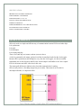
A touch screen is a 2-dimensional sensing device that is constructed of 2 sheets of material
separated slightly by spacers. A common construction is a sheet of glass providing a stable bottom
layer and a sheet of Polyethylene (PET) as a flexible top layer. The 2 sheets are coated with a
resistive substance, usually a metal compound called Indium Tin Oxide (ITO). The ITO is thinly
and uniformly sputtered onto both the glass and the PET layer. Tiny bumps called spacer dots are
then added to the glass side, on top of the resistive ITO coating, to keep the PET film from sagging,
causing an accidental or false touch.
When the PET film is pressed down, the two resistive surfaces meet. The position of this meeting
(a touch) can be read by a touch screen controller circuit
TOUCH SCREEN CONTROLLER (ADS7843):
FPGA is a digital device hence it can process only digital input and gives digital output. The output
of a Resistive touchscreen is analog. Hence to convert the analog output to digital an analog to
digital converter touch screen controller is used. Texas instrument’s ADS7843 touch screen
controller is used for this.
SPECIFICATION:
●4-WIRE TOUCH SCREEN INTERFACE
● RATIOMETRIC CONVERSION
● SINGLE SUPPLY: 2.7V to 5V
● UP TO 125kHz CONVERSION RATE
● SERIAL INTERFACE
● PROGRAMMABLE 8- OR 12-BIT RESOLUTION
● 2 AUXILIARY ANALOG INPUTS
● FULL POWER-DOWN CONTROL
SPI BUS INTERFACE
SPI can be used as a simple and efficient way of communication between FPGAs and other chips.
It is synchronous.
It is serial.
It is full-duplex.
It is not plug-and-play.
There is one (and only one) master, and one (or more) slaves.
A clock is generated by the master, and one bit of data is transferred each time the clock toggles.
Because SPI is synchronous and full-duplex, every time the clock toggles, two bits are actually
transmitted (one in each direction). MOSI is the "master output" while MISO is the "slave output".
FPGA is the master and ADC is the slave in this case.
The master pulls SS down to indicate to the slave that communication is starting .
SPI can easily achieve a few Mbps (mega-bits-per-seconds). That means it can be used for
uncompressed audio, or compressed video.
CODE
module spi(
CLK, RSTn,
TOUCH_CS,
TOUCH_IRQ,
TOUCH_BY,
TOUCH_CLK,
TOUCH_MISO,
TOUCH_MOSI,
test
);
input CLK; //50 Mhz
input RSTn; //assign switch
input TOUCH_BY;
output TOUCH_CS ; //make gnd
// input TOUCH_IRQ;
inout TOUCH_IRQ; //penirq
output TOUCH_CLK; // ads clock
input TOUCH_MISO; //from ads data
output TOUCH_MOSI; // to ads control register
output [3:0] test;
reg TOUCH_CSr;
reg TOUCH_CLKr;
reg TOUCH_MOSIr; // check
// Check the errer
reg [7:0] count_irq;
reg IRQ_FLAG;
always @(posedge CLK or negedge RSTn)
if (!RSTn) begin
count_irq <= 8'd0;
IRQ_FLAG <= 1'b0;
end
else if (count_irq == 8'd20)
begin
count_irq <= 8'd0;
IRQ_FLAG <= 1'b1;
end
else
count_irq <= count_irq + 1'b1;
assign TOUCH_IRQ = (IRQ_FLAG)?1'BZ:1'b0;
//
reg [7:0] count_500ns;
parameter T500ns = 8'd24 ;// 25 * 20ns = 500ns = 0.5us
reg spi_clk_flag;
// *** ************************************************
`define spi_clk_open 1'b1 ;
`define spi_clk_close 1'b0 ;
// *********************************** ****************
always @( posedge CLK or negedge RSTn)
if (! RSTn)
count_500ns <= 8'd0;
else if (count_500ns == T500ns || (!spi_clk_flag))
count_500ns <= 8'd0;
else if (spi_clk_flag)
count_500ns <= count_500ns + 1'b1;
reg [7:0] count_2us;
reg count_2us_flag;
// **** *********************************************
`define count_2us_open 1'd1
`define count_2us_close 1'd0
// ************************************** ***********
always @ ( posedge CLK or negedge RSTn)
if (!RSTn)
count_2us <= 8'd0;
else if (count_2us == 8'd99||(!count_2us_flag ))
count_2us <= 8'd0;
else if (count_2us_flag)
count_2us <= count_2us + 1'b1;
else
count_2us <= count_2us;
// ****** **************************************************
`define touch_clk_pos 8'd2
`define touch_clk_neg T500ns / 2
`define High
1'b1
`define low
1'b0
// ******************* *******************************************
parameter touch_cmd_x = 8'b1001_0000 ;// x_pos
parameter touch_cmd_y = 8'b1101_0000 ;// Y_POS
reg [15:0] state_touch;
reg [7:0] count_cmd_bit;
reg [7:0] count_dat_bit; // check
reg [11:0] touch_x1data;
reg [11:0] touch_x2data;
reg [7:0] count_sample;
always @(posedge CLK or negedge RSTn)
if (!RSTn)
begin
state_touch <= 8'D0;
spi_clk_flag <= `spi_clk_close;
count_cmd_bit <= 8'd0;
count_sample <= 8'd0;
end
else
case (state_touch)
8'd0:
if (!TOUCH_IRQ) //PENIRQ pulls low when a touch event occurs
begin
state_touch <= 8'd1;
count_sample <= 8'd0;
TOUCH_CSr <=`low;
spi_clk_flag <= `spi_clk_close;
count_2us_flag <= `count_2us_close;
TOUCH_CLKr <= `low;
end
else
begin
state_touch <= 8'd0;
TOUCH_CSr <= `High;
TOUCH_CLKr <= `low;
end
8'd1:
begin
state_touch <= 8'd2;
spi_clk_flag <= `spi_clk_open; //start spi clk 50ns or 2Mhz frequency
TOUCH_CSr <= `low; //slave select
count_cmd_bit <= 8'd9; //to count MOSI control register bits
count_dat_bit <= 8'd12;
end
8'd2 :
// Write control bits
if (count_500ns == `touch_clk_pos) // wait posedge clk
begin
state_touch <= 8'd3;
TOUCH_CLKr <= `low;
TOUCH_MOSIr <= touch_cmd_x [count_cmd_bit-2'b10];
count_cmd_bit <= count_cmd_bit-1'b1;
end
else
state_touch <= 8'd2;
8'd3:
if (count_cmd_bit == 8'D0) // count cmd bit =0 indicates that all the control bits are transfered now
conversion can be achievec
begin
TOUCH_MOSIr <= 1'd0;
TOUCH_CLKr <= `low;
if (count_2us == 8'd99)
begin
state_touch <= 8'd4;
count_2us_flag <= `count_2us_close;
count_dat_bit <= 8'd12;
spi_clk_flag <=`spi_clk_open;
end
else
begin
state_touch <= 8'd3;
count_2us_flag <= `count_2us_open;
spi_clk_flag <= `spi_clk_close;
end
end
else if (count_500ns == `touch_clk_neg)
begin
state_touch <= 8'd2; // to run the loop till all the control bits are transfered
TOUCH_CLKr <= `High;
end
else
state_touch <= 8'd3;
8'd4:
// Read Data
if (count_500ns == `touch_clk_neg)
// wait negedge clk
begin
state_touch <= 8'd5;
TOUCH_CLKr <= `High;
touch_x1data [count_dat_bit-1'b1] <= TOUCH_MISO;
end
else
state_touch <= 8'd4;
8'd5:
begin
state_touch <= 8'd6;
count_dat_bit <= count_dat_bit - 1'b1;
end
8'd6:
if (count_dat_bit == 8'D0)
begin
state_touch <= 8'd7;
TOUCH_CLKr <= `low;
end
else if (count_500ns == `touch_clk_pos)
begin
TOUCH_CLKr <= `low;
state_touch <= 8'd4;
end
else
state_touch <= 8'd6;
8'd7:
begin
state_touch <= 8'd8;
spi_clk_flag <= `spi_clk_close;
TOUCH_CSr <= `High;
end
// Close the spi Clock
8'd8:
if (count_2us == 8'd99)
begin
state_touch <= 8'd9;
count_2us_flag <= `count_2us_close;
end
else
begin
state_touch <= 8'd8;
count_2us_flag <= `count_2us_open;
end
8'd9:
begin
state_touch <= 8'd10;
spi_clk_flag <= `spi_clk_open; //start spi clk 50ns or 2Mhz frequency
TOUCH_CSr <= `low;
count_cmd_bit <= 8'd9; //to count MOSI control register bits
count_dat_bit <= 8'd12;
end
8'd10 :
// Write control bits
if (count_500ns == `touch_clk_pos) // wait posedge clk
begin
state_touch <= 8'd11;
TOUCH_CLKr <= `low;
TOUCH_MOSIr <= touch_cmd_y [count_cmd_bit-2'b10];
count_cmd_bit <= count_cmd_bit-1'b1;
end
else
state_touch <= 8'd10;
8'd11:
if (count_cmd_bit == 8'D0) // count cmd bit =0 indicates that all the control bits are transfered now
conversion can be achievec
begin
TOUCH_MOSIr <= 1'd0;
TOUCH_CLKr <= `low;
if (count_2us == 8'd99)
begin
state_touch <= 8'd12;
count_2us_flag <= `count_2us_close;
count_dat_bit <= 8'd12;
spi_clk_flag <=`spi_clk_open;
end
else
begin
state_touch <= 8'd11;
count_2us_flag <= `count_2us_open;
spi_clk_flag <= `spi_clk_close;
end
end
else if (count_500ns == `touch_clk_neg)
begin
state_touch <= 8'd10; // to run the loop till all the control bits are transfered
TOUCH_CLKr <= `High;
end
else state_touch <= 8'd11;
8'd12:
// Read Data
if (count_500ns == `touch_clk_neg)
// wait negedge clk
begin
state_touch <= 8'd13;
TOUCH_CLKr <= `High;
touch_x2data [count_dat_bit-1'b1] <= TOUCH_MISO;
end
else
state_touch <= 8'd12;
8'd13:
begin
state_touch <= 8'd14;
count_dat_bit <= count_dat_bit - 1'b1;
end
8'd14:
if (count_dat_bit == 8'D0)
begin
state_touch <= 8'd15;
TOUCH_CLKr <= `low;
end
else if (count_500ns == `touch_clk_pos)
begin
TOUCH_CLKr <= `low;
state_touch <= 8'd12;
end
else
state_touch <= 8'd14;
8'd15:
begin
state_touch <= 8'd16;
spi_clk_flag <= `spi_clk_close; // Close the spi Clock
TOUCH_CSr <= `High;
end
8'd16:
if (count_2us == 8'd99)
begin
state_touch <= 8'd0;
count_2us_flag <= `count_2us_close;
end
else
begin
state_touch <= 8'd16;
count_2us_flag <= `count_2us_open;
end
endcase
assign TOUCH_CLK = TOUCH_CLKr;
assign TOUCH_CS = TOUCH_CSr;
assign TOUCH_MOSI = TOUCH_MOSIr;
assign test = touch_x1data [ 3 : 0 ]; // display the data collected fourth place
endmodule
FUTURE IMPROVEMENTS
The touch screen can be mounted on a LCD module. Thus, the LCD Touch screen module can be used
to develop further applications such as drawing pad.