1
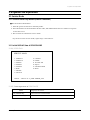
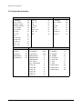
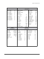
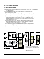
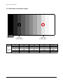
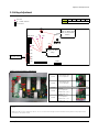
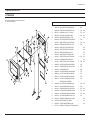
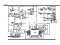
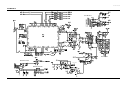
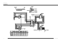
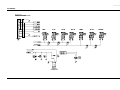
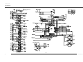
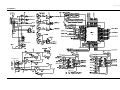
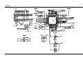
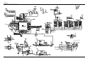
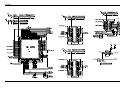
PLASMA DISPLAY TV
Chassis :
Model:
SERVICE
D62B
PPM50H3QX/EDC
Manual
PLASMA DISPLAY TV
CONTENTS
1.
Specifications
2.
Alignment and Adjustments
3.
Exploded View and Parts List
4.
Service Item
5.
Schematic Diagrams
Specifications
1. Specifications
MODEL
PPM50H3Q
Dimensions
Display
1204.6(W) x 79(D) x 7245(H) mm / 47.43(W) x 3.11(D) x 28.5(H) inches
Weight
Display
43 Kg (without stand)
Screen Size
Voltage
Power Consumption
50 Inches
AC 120V, 60Hz / AC 100-250V, 50/60Hz
490 Watts
Number of Pixels
1366(H) X 768(V)
External Control
RS-232C IN(Mini jack), RS-232C OUT(D-SUB 9P)
AUDIO Input
VIDEO / S-VIDEO
COMPONENT 1
COMPONENT 2
RGB(PC) 1/2
DVI
External Speaker (10W+10W)
AUDIO Output
Audio Output (L/R RCA)
VIDEO
VIDEO Input
VIDEO Output
Samsung Electronics
S-VIDEO
COMPONENT 1 - 480i / 480p / 720p / 1080i
COMPONENT 2/RGB2(PC) IN (BNC, 5P, 480i~1080i, VGA~XGA)
RGB1(PC1) - D-SUB 15P
DVI
Monitor Output (RCA)
1-1
MEMO
1-2
Samsung Electronics
Alignment and Adjustments
2. Alignment and Adjustments
2-1 Service Mode
2-1-1 SERVICE MODE Entry Method (General Transmitter)
■ For the General Transmitter
1. Turn the power off and set to stand-by mode.
2. Press the buttons of the transmitter in this order; Info-Menu-Mute-Power or Mute-1-8-2-power
to turn the set on.
3. The set turns on and enters service mode.
* If you fail to enter service mode, repeat steps 1 and 2 above.
2-1-2 Initial DISPLAY State of SERVICE MODE
2-1-2(A) OSD DISPLAY
SERVICE MAIN
1. VSP9437-1
2. VSP9437-2
3. FLI2300
4. ASI500-1
5. ASI500-2
6. DNIe
7. AD9888
8. CXA2151
9. CXA2101
10. LOGIC
11. TP LOG-ASI
12. Option
13. CheckSum 0000
14. Reset
Release : 2003-07-12 T_NEW 50MWW_1001
2-1-2(B) Button Operations in SERVICE MODE
Menu
Displays all menus
UP/DOWN Key
Cursor move to select items
LEFT/RIGHT Key
Enable to increase and decrease the data of the selected items
Samsung Electronics
2-1
Alignment and Adjustments
2-1-3 Factory Data Initial Value
VSP9437-1(Video)
V PEAKING
16
PAL 60
HPLL SPEED
00
PAL
RGB/YUV CONT
36
PAL
RGB/YUV BRIGHT
00
SECAM
YUV SATCB
26
NTSC
YUV SATCR
26
PAL B/G
01
PAL D/K
01
NR
PAL I
01
SECAM B/G
27
SECAM D/K
27
SECAM L’/L
27
NTSC
01
M
NTSC 4.43
27
V PEAKING
01
HPLL SPEED
00
01
PAL
01
27
SECAM
27
01
NTSC
01
NTSC 4.43
27
PAL AV
01
PAL
27
SECAM AV
27
01
NTSC AV
01
M
60
16
27
FLI2300
2-2
VSP9437-2(Video)
ASI500
(Video/PC,DVI)
Y DELAY
05
R CONTRAST
32/30
FILTER YPASS
0
C DELAY
12
G CONTRAST
32/30
R GAMMA
32
CONTRAST
95
B CONTRAST
32/30
G GAMMA
32
BRIGHTNESS
185
R BRIGHTNESS
0
B GAMMA
32
SATURATION
110
G BRIGHTNESS
0
H POSITION
0
B BRIGHTNESS
0
V POSITION
0
TEXT ALPHA
1
H SIZE
0
TEXT THRESHOLD
7
V SIZE
0
FILTER ML
0
OVERSCAN R
50
FILTER MR
0
OVERSCAN G
50
FILTER FR
0
OVERSCAN B
50
FILTER MC
16
FILTER UC
0
FILTER LC
0
Samsung Electronics
Alignment and Adjustments
ASI500
DNIe
(Video/PC,DVI)
PIP R CONT
32
BRIGHT OFFSET
TH CORING
02
PIP G CONT
32
Attachment
PATT SEL
00
PIP B CONT
32
CONTRA OFFSET
NOISE TH3
100
PIP R BRIGHT
0
Attachment
H CONT
32
PIP G BRIGHT
0
SCALE MAX Y
48
V CONT
32
PIP B BRIGHT
0
SCALE MIN Y
16
BLACK GAIN
375
PIP FILTER IC
0
TH HPF
00
WHITE GAIN
375
PIP FILTER ML
0
TH EDGE
04/05
WTE GAIN
300
PIP FILTER MR
0
NR SEL
02
CTE GAIN
PIP FILTER UC
0
CE UPPER
176
220/240
H SHARP GAIN
127/48
45
V SHARP GAIN
127/48
CE CUTOFF
CE GAIN
64/75
SHARPNESS
DCE GAIN
190/96
CLK DLY
07
H POSI
12
SKIN ON
00
CTI GAIN
08
DE NOISE GAIN
100
08/10
AD9888
CXA2101
Video/Comp/PC
(Video,COMP)
R GAIN
71/128/83
PICTURE
16
SUB BRIGHT
35
G GAIN
77/122/81
HUE
31
CR OFFSET1
07
B GAIN
95/128/81
COLOR
16
CB OFFSET1
07
R OFFSET
63/79/64
BRIGHT
61
SUB CONT
12
G OFFSET
66/53/70
SHARPNESS
28
SUB COL
08
B OFFSET
64/82/68
R DRIVE
4
SUB HUE
08
G DRIVE
4
R-Y/R
13
V-PATH
PC
AUTO COLOR
B DRIVE
4
R-Y/B
15
OFF
R CUTOFF
32
G-Y/R
12
G CUTOFF
32
G-Y/B
04
B CUTOFF
32
Samsung Electronics
2-3
Alignment and Adjustments
LOGIC
TP LOG-ASI
(PDP DRIVER)
(TEST PAT LOGIC/SCALER)
R DRIVE
Attachment
ACTIVE VPOS
12
LOG PATTERN
0
G DRIVE
Attachment
ACTIVE HPOS
19
LOG HIGH LEVEL
0
B DRIVE
Attachment
VSYNC POS
3
LOG LOW LEVEL
0
R CUTOFF
Attachment
HSYNC POS
32
ASI COLORBAR
0
G CUTOFF
Attachment
VSYNC WIDTH
2
B CUTOFF
Attachment
HSYNC WIDTH
12
GAMMA
1
GTS SET
1
ERD MODE
2
RANDOM NOISE
1
DIFF FILTER
1
APC
1
APC SET
0
APC VALUE
127
*CXA2151 Data
00. Gam Sel 01
01. CB Gain 07
02. CR Gain 07
03. Y Gain
01
04. V TC
01
IC
SNI
Logic
2-4
Item
W/B Data
Video,S-VHS
Component
PC
DVI
Bright
41
44
39
39
Contrast
58
57
67
49
R Gain
140
139
132
134
G Gain
128
130
130
130
B Gain
122
119
125
120
R Cutoff
07
244
03
02
G Cutoff
0
0
0
0
B Cutoff
17
248
247
251
Samsung Electronics
Alignment and Adjustments
Alignment and Adjustments
2-2 WHITE Balance Coordinates
2-2-1 White Balance Adjustment
1. W/B Adjustment is required for the following four modes: DVI → DTV → PC → CVBS(VIDEO)
→ CVBS(VIDEO PIP)
2. Adjustment Method (DVI, DTV, PC : VG828, CVBS : Adjust RF signals to match the
Toshiba pattern (in-house signal)
! Adjust the target set by adjusting the panel logic and the video DNIe adjustment register in
register in order to determine the referential W/B of the panel with a DVI input, which
is the full digital path.
@ For DTV adjustment, adjust the adjustment register of ad9888 to align the DTV signal
to the DNIe and logic panel value which was fixed with a DVI adjustment so that they are
in effect considered to be the same signals. (At this time, do not adjust the gain of
AD9888 → the Highlight W/B does not need to be adjusted since its deviation falls
within valid distribution range.)
# PC adjustment is same as DTV adjustment. (The offset can be applied to the values
obtained through DTV adjustment. However, additional adjustment is required for
Y, Cb, and Cr of DTV since PC processes R, G, and B signals.)
$ cvbs adjustment is performed with the Toshiba pattern (in-house signal) and differs
from the VG828 signals in the above three modes. Hence, it should be performed with
the same method of ! DVI adjustment.
% Finally, activate PIP in video mode, and repeat W/B adjustment.
❈ Thus, Micom saves the W/B data separately for each memory mode of the block
(See the block diagram given below) during W/B adjustment.
Micom can memorize the four modes
separately. However, under the current
adjustment guidelines, DTV and PC are
memorized with the same value during
DVI adjustment and CVBS is memorized
with a separate value.
Samsung Electronics
2-5
Alignment and Adjustments
2-2-2 White Balance Coordinates by Mode
Pedestal Level
H/L
L/L
2-6
Low Light
measure point
High Light
measure point
Video
Component
PC
DVI
x
278
280
280
280
y
285
287
295
295
Y(fL)
33
34
28
31
x
278
280
285
285
y
285
287
295
295
Y(fL)
1.3
0.6
1.2
1.0
Samsung Electronics
Alignment and Adjustments
2-3 Voltage Adjustment
Output
Test Point
Vo ltage
VR : Variable Resi sto r
Va
Vsc
Vs
Ve
Vse t
See t he labels attached on the base chassis
Pin Connector
VR2
Vs
Adjust the SMPS voltage
using the VR(Var iable
Resistor)
Vs
Vset
CN805 CN812
Ve
(
SMPS
Va
CN804
VR1
Vscan
Va
CN806
Validate the SMPS
voltage
CN807
Fan power sour ce.
CN808
CN809
CN810
CN803
CN802
CN801
SMPS Volume Resistor Adjustment
Point 1
Point 1
Volume Resistor VR2
VR2
for "Vs" Adjustment
Point 4
Point 2
Point 2
Point 3
VR1
Volume Resistor VR1
for "Va" Adjustment
Volume Resistor VR6 is a Factory Setting Point. Don’ t touch.
Test Point
Point 5
Point 3
for "Vs" Adjustment
Point 4
CN805
CN804
CN 805 Pin No. 9, 10 or
CN 804 Pin No. 8, 9
Test Point
for "Va" Adjustment
Point 5
CN 812 Pin No. 1, 2 or
CN 806 Pin No. 1, 2
CN812
CN806
☞ Notes
1. When the SMPS-PCB is replaced, the Va, Vsc, Vs, Ve and Vset voltages must be checked and adjusted to the proper levels
indicated on the panel sticker.
Samsung Electronics
2-7
MEMO
2-8
Samsung Electronics
Exploded View & Parts List
3. Exploded View & Parts List
3-1 PPM50H3QX/EDC
You can search for the updated part code through ITSELF web site.
URL : http://itself.sec.samsung.co.kr
No
Code No
1
BN96-00172Q
1-1
Q’ty
Remark
ASSY COVER P-FRONT;50P3H(VMB),ASIA,HIPS
1
M0003
BN64-00098N
CABINET-FRONT;50P3 VMB,HIPS,HB,HF-1690H,
1
T0003
S.N.A
1-2
BP64-00177A
BADGE-BRAND;ALL,AL,T1.5,70,11.3,BLK,SILI
1
T0057
S.N.A
1-3
BP64-00045B
KNOB CONTROL;P3,ABS,HB,GRY,SVM3012
1
T0022
S.N.A
1-4
BN64-00074B
WINDOW-REMOTE;42P3S,PMMA,,,,,,CLEAR
1
2
BN94-00494C
ASSY PCB MISC-CONTROL;SPD-50P3H,D56A/D59
1
T0098
3
6003-001026
SCREW-TAPTITE;RH,+,B,M4,L15,ZPC(BLK),SWR
3
T0081
4
BN64-00125A
SCREEN-EMI,FITER;FILTER,50P3,T47%,1155+6
1
T0055
5
BN61-00262D
BRACKET-FILTER TOP ASSY;50P3H,AL5052,T1.
1
S.N.A
6
BN61-00263D
BRACKET-FILTER SIDE LEFT;50P3H,AL5052,T1
1
S.N.A
7
BN61-00197A
BRACKET-FILTER,SIDE;50P3H,AL5052,T1.2
1
S.N.A
8
BN61-00264D
BRACKET-FILTER BOT ASSY;50P3H,AL5052,T1.
1
S.N.A
9
6003-001026
SCREW-TAPTITE;RH,+,B,M4,L15,ZPC(BLK),SWR
10
10
BN61-00967A
HOLDER-MODULE;50P3H,AL DIECASTING
4
11
6003-001026
SCREW-TAPTITE;RH,+,B,M4,L15,ZPC(BLK),SWR
8
T0081
12
BN96-00985A
ASSY PDP P-MODULE;M3,S50HW-XD03,D66A,D3.
1
T0044
13
6006-001126
SCREW-MACHINE;WSP,PH,+,M5,L12,NI PLT,SWR
4
CCM1
14
BN61-00674A
STAND-BASE;PPM42S3,PPS
2
M0412
15
BN94-00494U
ASSY PCB MISC-SMPS;SPD-50P4HD,D66A,DAVIN
1
T0124
16
BN96-00999A
ASSY PDP P-X MAIN BOARD;LJ92-00852A,S50H
1
T0073
17
BN96-01001A
ASSY PDP P-Y MAIN BOARD;LJ92-00853A,S50H
1
T0096
18
BN96-01012A
ASSY PDP P-LOGIC MAIN BOARD;LJ92-00949A,
1
T0037
GUIDE-STAND;50P3H,AL DIECASTING
2
19
Samsung Electronics
Description;Specification
S.N.A
T0081
S.N.A
S.N.A
S.N.A
S.N.A
20
BN96-00266D
ASSY COVER P-BACK SUB;PPM50H3,AL3032 T1.
1
T0008
S.N.A
21
BN31-00001A
FAN-ASSY;G4020S05B2-RS,PBTP,UL94-Vo,Brac
3
T0243
22
6006-001035
SCREW-ASS’Y MACH;WSP,PH,+,M3,L8,ZPC(YEL)
8
EL013
S.N.A
23
BN94-00559A
ASSY PCB MISC-DIGITAL;PPM50H3QX/XEU,D62B
1
T0132
S.N.A
24
BN94-00560A
ASSY PCB MISC-ANALOG;PPM50H3QX/XEU,D62B,
1
T0145
S.N.A
25
BN96-00173C
ASSY COVER P-BACK;PPM50H3,AL3032 T1.2,DG
1
T0001
25-1
BN63-00531B
COVER-BACK SUB;PPM50H3,AL3032,1.2,VMB,DG
1
S.N.A
25-2
BN61-00202B
BRACKET-HANDLE;42P3,T1.5,DGM5233
2
S.N.A
26
BN96-00286F
ASSY MISC P-BRACKET TERMINAL;P3,VMB
1
S.N.A
27
6006-001194
SCREW-ASSY TAPT;WP,BH,+,M4,L20,ZPC(BLK),SWRCH18A 4
3-1
Service Item
4. SERVICE ITEM
You can search for the updated part code through ITSELF web site.
URL : http://itself.sec.samsung.co.kr
Loc.
Code No
Description;Specification
Q’ty
D0254
AA32-00013B
MODULE REMOCON;346HF5,38KHz,940mm,MESH,H
1
T0074
BN59-00366A
REMOCON;TM76,D61A,42,G6148,PPM42S3,EX
1
T0055
BN64-00125A
SCREEN-EMI,FITER;FILTER,50P3,T47%,1155+6
1
T0098
BN94-00494C
ASSY PCB MISC-CONTROL;SPD-50P3H,D56A/D59
1
T0124
BN94-00494U
ASSY PCB MISC-SMPS;SPD-50P4HD,D66A,DAVIN
1
M0003
BN96-00172Q
ASSY COVER P-FRONT;50P3H(VMB),ASIA,HIPS
1
T0001
BN96-00173C
ASSY COVER P-BACK;PPM50H3,AL3032 T1.2,DG
1
M0764
BN96-00756A
ASSY STAND P-SCREW;PPM50H3,SCREW+PE-BAG,
1
T0044
BN96-00985A
ASSY PDP P-MODULE;M3,S50HW-XD03,D66A,D3.
1
T0073
BN96-00999A
ASSY PDP P-X MAIN BOARD;LJ92-00852A,S50H
1
T0096
BN96-01001A
ASSY PDP P-Y MAIN BOARD;LJ92-00853A,S50H
1
T0111
BN96-01002A
ASSY PDP P-Y BUFF UPPER BOARD;LJ92-00880
1
T0112
BN96-01003A
ASSY PDP P-Y BUFF DOWN BOARD;LJ92-00881A
1
T0113
BN96-01004A
ASSY PDP P-E BUFFER BOARD;LJ92-00917A,S5
1
T0114
BN96-01005A
ASSY PDP P-F BUFFER BOARD;LJ92-00918A,S5
1
T0115
BN96-01006A
ASSY PDP P-G BUFFER BOARD;LJ92-00919A,S5
1
T0116
BN96-01007A
ASSY PDP P-H BUFFER BOARD;LJ92-00920A,S5
1
T0117
BN96-01008A
ASSY PDP P-I BUFFER BOARD;LJ92-00921A,S5
1
T0118
BN96-01009A
ASSY PDP P-J BUFFER BOARD;LJ92-00922A,S5
1
BN96-01010A
ASSY PDP P;LJ92-00923A,S50HW-XD03,D66A,D
1
T0119
BN96-01011A
ASSY PDP P-LOGIC SUB(RIGHT)BD;LJ92-00959
1
T0037
BN96-01012A
ASSY PDP P-LOGIC MAIN BOARD;LJ92-00949A,
1
Samsung Electronics
S.N.A
4-1
Service Item
MEMO
4-2
Samsung Electronics
Schematic Diagrams
5. Schematic Diagrams
5-1 ANALOG 1
Analog - Digital Board
Connector
This Document can not be used without Samsung’s authorization.
S-Video
Video IN
Video/S-Video Sound
CXA2151Q
IC103
COMPONENT1
Samsung Electronics
5-1
Schematic Diagrams
5-2 ANALOG 2
This Document can not be used without Samsung’s authorization.
3D COMB FILTER
To DC FAN
R246
R247
TILT SENSOR
FAN PART
50"
5-2
Samsung Electronics
Schematic Diagrams
5-3 ANALOG 3
This Document can not be used without Samsung’s authorization.
From SMPS Board
External Speaker
BD701
MONITOR OUT VIDEO
1
2
+12V_AMP
MONITOR OUT SOUND
Samsung Electronics
5-3
Schematic Diagrams
5-4 ANALOG 4
This Document can not be used without Samsung’s authorization.
74HCT573
74HCT573
5-4
Samsung Electronics
Schematic Diagrams
5-5 CONTROL
This Document can not be used without Samsung’s authorization.
AA32-00013B
Samsung Electronics
5-5
Schematic Diagrams
5-6 DIGITAL 1
This Document can not be used without Samsung’s authorization.
Analog - Digital board
Connector
42 SD
42 HD
50,63 HD
PC(D-SUB&DVI) SOUND
5-6
Samsung Electronics
Schematic Diagrams
5-7 DIGITAL 2
This Document can not be used without Samsung’s authorization.
BNC Connector
PC D-SUB
ANALOG EDID EPROM
IC306
LF33CDT
1
IN
OUT
3
GND
2
From SMPS board
Samsung Electronics
5-7
Schematic Diagrams
5-8 DIGITAL 3
This Document can not be used without Samsung’s authorization.
5-8
Samsung Electronics
Schematic Diagrams
5-9 DIGITAL 4
This Document can not be used without Samsung’s authorization.
DVI Connector
DIGITAL EDID EPROM
Samsung Electronics
5-9
Schematic Diagrams
5-10 DIGITAL 5
This Document can not be used without Samsung’s authorization.
Samsung Electronics
5-10
Schematic Diagrams
5-11 DIGITAL 6
This Document can not be used without Samsung’s authorization.
USER EPROM (256K)
Flash Memory
B12 : 1204-002105
From Remote Control board
RS232C OUT
RS232C IN
5-11
Samsung Electronics
Schematic Diagrams
5-12 DIGITAL 7
This Document can not be used without Samsung’s authorization.
Samsung Electronics
5-12
Schematic Diagrams
5-13 DIGITAL 8
This Document can not be used without Samsung’s authorization.
LVDS Connector
5-13
Samsung Electronics
ELECTRONICS
This Service Manual is a property of Samsung Electronics Co.,Ltd.
Any unauthorized use of Manual can be punished under applicable
International and/or domestic law.
© Samsung Electronics Co., Ltd. May. 2004
Printed in Korea
AA82-01607A