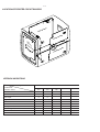
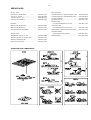
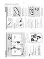
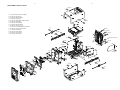
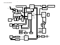
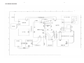
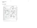
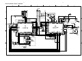
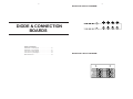
1
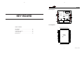
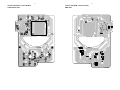
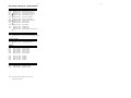
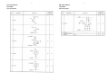
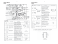
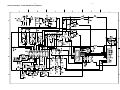
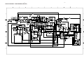
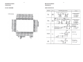
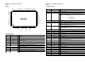
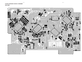
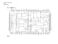
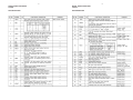
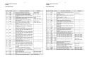
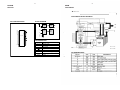
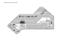
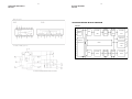
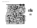
Micro System
MC-M350/21/22/25
Service
Service
Service
Service Manual
TABLE OF CONTENTS
Page
Location of PCBs & Version Variations ...................... 1-2
Technical Specifications ............................................. 1-3
Measurement setup .................................................... 1-4
Service Aids, Safety Instruction, etc. .......................... 1-5
Preparations & Controls ............................................. 1-7
Disassembly Instructions ............................................... 2
Set Block diagram ......................................................... 3
Set Wiring diagram ........................................................ 4
Key Board ...................................................................... 5
Power Board .................................................................. 6
Tuner Board ................................................................... 7
MCU & CD Board .......................................................... 8
Diode & Connection Boards........................................... 9
Main Board .................................................................. 10
Set Mechanical Exploded View & Parts List ............... 11
©
Copyright 2002 Philips Consumer Electronics B.V. Eindhoven, The Netherlands
CLASS 1
LASER PRODUCT
All rights reserved. No part of this publication may be reproduced, stored in a retrieval system
or transmitted, in any form or by any means, electronic, mechanical, photocopying, or otherwise
without the prior permission of Philips.
Published by SL 0325 Service Audio
Version 1.0
Printed in The Netherlands
Subject to modification
GB
3140 785 32550
1-2
LOCATION OF PRINTED CIRCUIT BOARDS
IN
MA
AR
BO
D
I
B OD
O E
A
R
D
D
M
C
B U
O &
A C
R D
D
K
E
B Y
O
A
R
R
OA
RB
D
NE
TU
D
D
AR
BO
R
WE
PO
VERSION VARIATIONS
Type/Versions
MC-M350
Features &
Board in used
RDS function
ECO Standby
Aux Input
/21
/22
/25
x
x
x
x
x
x
x
x
x
x
x
x
Digital Coaxial Out
Line Out
Subwoofer Out
Headphone Out
AC Voltage Selector
Non-Cenelec Tuner
Cenelec Tuner
x
x
1-3
SPECIFICATIONS
GENERAL:
Mains voltage
/21 : 120V / 230V ±15%
Switchable
/22/25 : 230V ±10%
Maximum Sensitivity
Sensitivity at 26dB S/N
: < 1.5mV/M
: < 6.0mV/M
Selectivity at S9/300kHz
: > 24dB
IF rejection
: > 26dB
Image rejection
Distortion I/P:5~50mV
: > 20dB
: < 5%
/22/25 : 50Hz
Modulation Hum with REC on
: > 40dB
/22/25 : < 1W at ECO Standby
: < 9W at Standby
AMPLIFIER:
Mains frequency
/21 : 50/60Hz
Power consumption
(DEMO mode off)
: 53W at Active
Clock accuracy
: < 4 seconds per day
Dimension centre unit
: 155 x 220 x 270mm
TUNER:
Output power (6Ω, 1kHz, 10% THD) : 30W
Frequency response within -3dB
: 60Hz-14kHz
Digital Sound Control (DSC)
: Optimal,Classic,Jazz,
DBB
Incredible Surround (IS)
: ON/OFF
: ON/OFF
Rock
Input sensitivity (±3dB) for Rated Output Power at 1kHz
FM
Aux in
Tuning range
IF frequency
: 87.5-108MHz
: 10.7MHz ± 20kHz
Aerial input
: 75Ω Coaxial
Sensitivity at 26dB S/N
: < 22dBf
Tuner in
CD in
Tape in
: 500mV; Rs=600Ω
: FM67.5kHz, AM80%Modulation
: -6dB track
: 250nWb/m
Output sensitivity
Selectivity at S9/300kHz
IF Rejection
: > 33dB
: > 60dB
Image Rejection
: > 20dB
CASSETTE RECORDER:
Distortion at RF=1mV, dev. 75kHz
: < 3%
Number of track
: 2 Tracks (Stereo)
-3dB Limiting point
: < 23.5dB
Tape speed
: 4.76 cm/sec ± 2%
Crosstalk at RF=1mV, dev. 40kHz
Modulation Hum
: > 26dB
: > 45dB
Wow and flutter
Fast-wind/Rewind time C60
: < 0.4% DIN
: 130 sec
AM Suppression I/P: 48~82dBf
: > 25dB
Bias system
: 78kHz ± 10kHz
Rec/Pb freq. response within 8dB
: 80Hz - 10kHz
AM (MW)
Tuning range
Headphone output at 32Ω : 15mW ± 2dB
Signal to Noise Ratio (A-weighted) : ≥ 48dBA
/21/22/25 : 531-1602kHz
Distortion 250nWb/m
Channel Difference at overall
: < 5%
: < 4dB
/21 : 530-1700kHz
Grid
IF frequency
/21 : 9kHz / 10kHz
/22/25 : 9kHz
: 450kHz ± 1kHz
Aerial input
: Frame aerial 18.1µH
COMPACT DISC:
Frequency response within ± 3dB : 63Hz - 14kHz
Output level (in Vrms)
: 500mV, Zout = 100Ω
Signal/Noise ratio (A-weighted) : > 62dBA
Sensitivity at 26dB S/N
: < 3.25mV/M
Distortion at 1kHz
: < 0.02%
Selectivity at S9/300kHz
AGC Figure of Merit
: > 15dB
: > 25dB
Channel unbalance at 1kHz
: ≤ 2dB
IF rejection
: > 24dB
Channel separation at 1kHz
Emphasis
: > 30dB
: 15/50 µS (switched
Image rejection
: > 20dB
Distortion at RF=50mV, m=80%
Mudulation Hum with REC or
: < 5%
: > 40dB
Spurious Response Rejection
: > 28dB
automatically)
THD Noise(1kHz)
: 1.00%
Outband Attenuation
: > 20dB for Freq. > 40kHz
MP3 - CD :
LW (Only for /22/25 )
Tuning range
Grid
: 153-279kHz
: 3kHz
IF frequency
: 450kHz ± 1kHz
Aerial input
: Frame aerial 18.1µH
Bit rates
: 32K - 320Kps
Sampling rates
: 32KHz/44.1KHz/48KHz
1-4
MEASUREMENT SETUP
Tuner FM
DUT
RF Generator
Bandpass
250Hz-15kHz
LF Voltmeter
e.g. 7122 707 48001
e.g. PM2534
Ri=50Ω
e.g. PM5326
S/N and distortion meter
e.g. Sound Technology ST1700B
Use a bandpass filter to eliminate hum (50Hz, 100Hz) and disturbance from the pilottone (19kHz, 38kHz).
Tuner AM (MW,LW)
DUT
Bandpass
250Hz-15kHz
LF Voltmeter
e.g. 7122 707 48001
e.g. PM2534
RF Generator
e.g. PM5326
S/N and distortion meter
Ri=50Ω
e.g. Sound Technology ST1700B
Frame aerial
e.g. 7122 707 89001
To avoid atmospheric interference all AM-measurements have to be carried out in a Faraday´s cage.
Use a bandpass filter (or at least a high pass filter with 250Hz) to eliminate hum (50Hz, 100Hz).
Recorder
CD
Use Audio Signal Disc
(replaces test disc 3)
SBC429 4822 397 30184
Use Universal Test Cassette CrO2 SBC419 4822 397 30069
or Universal Test Cassette Fe
SBC420 4822 397 30071
LF Generator
DUT
e.g. PM5110
L
DUT
L
R
R
S/N and distortion meter
S/N and distortion meter
e.g. Sound Technology ST1700B
e.g. Sound Technology ST1700B
LEVEL METER
e.g. Sennheiser UPM550
with FF-filter
LEVEL METER
e.g. Sennheiser UPM550
with FF-filter
1-5
SERVICE AIDS
Service Tools:
ESD Equipment:
Universal Torx driver holder .................................. 4822 395 91019
Anti-static table mat - large 1200x650x1.25mm ... 4822 466 10953
Torx bit T10 150mm ............................................. 4822 395 50456
Anti-static table mat - small 600x650x1.25mm ..... 4822 466 10958
Torx driver set T6 - T20 ......................................... 4822 395 50145
Anti-static wristband .............................................. 4822 395 10223
Torx driver T10 extended ...................................... 4822 395 50423
Connector box (1MΩ) ............................................ 4822 320 11307
Extension cable
Cassette:
SBC419 Test cassette CrO2 ................................. 4822 397 30069
(to connect wristband to conn. box) .................. 4822 320 11305
Connecting cable
SBC420 Test cassette Fe ..................................... 4822 397 30071
(to connect table mat to conn. box) .................. 4822 320 11306
MTT150 Dolby level 200nWb/M ............................ 4822 397 30271
Earth cable (to connect product to mat or box) .... 4822 320 11308
Complete kit ESD3
Compact Disc:
SBC426/426A Test disc 5 + 5A ............................ 4822 397 30096
SBC442 Audio Burn-in Test disc 1kHz ................. 4822 397 30155
SBC429 Audio Signals disc .................................. 4822 397 30184
Dolby Pro-logic Test Disc ...................................... 4822 395 10216
HANDLING CHIP COMPONENTS
(combining all above products) ......................... 4822 320 10671
Wristband tester .................................................... 4822 344 13999
1-6
GB
NL
ESD
WARNING
Alle IC’s en vele andere halfgeleiders zijn
gevoelig voor electrostatische ontladingen
(ESD).
Onzorgvuldig behandelen tijdens reparatie kan
de levensduur drastisch doen verminderen.
Zorg ervoor dat u tijdens reparatie via een
polsband met weerstand verbonden bent met
hetzelfde potentiaal als de massa van het
apparaat.
Houd componenten en hulpmiddelen ook op
ditzelfde potentiaal.
All ICs and many other semi-conductors are
susceptible to electrostatic discharges (ESD).
Careless handling during repair can reduce life
drastically.
When repairing, make sure that you are
connected with the same potential as the mass
of the set via a wrist wrap with resistance.
Keep components and tools also at this
potential.
F
WAARSCHUWING
ATTENTION
I
Tous les IC et beaucoup d’autres
semi-conducteurs sont sensibles aux
décharges statiques (ESD).
Leur longévité pourrait être considérablement
écourtée par le fait qu’aucune précaution n’est
prise à leur manipulation.
Lors de réparations, s’assurer de bien être relié
au même potentiel que la masse de l’appareil et
enfiler le bracelet serti d’une résistance de
sécurité.
Veiller à ce que les composants ainsi que les
outils que l’on utilise soient également à ce
potentiel.
D
AVVERTIMENTO
WARNUNG
Alle ICs und viele andere Halbleiter sind
empfindlich gegenüber elektrostatischen
Entladungen (ESD).
Unsorgfältige Behandlung im Reparaturfall kan
die Lebensdauer drastisch reduzieren.
Veranlassen Sie, dass Sie im Reparaturfall über
ein Pulsarmband mit Widerstand verbunden
sind mit dem gleichen Potential wie die Masse
des Gerätes.
Bauteile und Hilfsmittel auch auf dieses gleiche
Potential halten.
Tutti IC e parecchi semi-conduttori sono
sensibili alle scariche statiche (ESD).
La loro longevità potrebbe essere fortemente
ridatta in caso di non osservazione della più
grande cauzione alla loro manipolazione.
Durante le riparazioni occorre quindi essere
collegato allo stesso potenziale che quello della
massa dell’apparecchio tramite un braccialetto
a resistenza.
Assicurarsi che i componenti e anche gli utensili
con quali si lavora siano anche a questo
potenziale.
GB
Safety regulations require that the set be restored to its original
condition and that parts which are identical with those specified,
be used.
“Pour votre sécurité, ces documents
doivent être utilisés par des spécialistes agréés, seuls habilités à réparer
votre appareil en panne”.
NL
Veiligheidsbepalingen vereisen, dat het apparaat bij reparatie in
zijn oorspronkelijke toestand wordt teruggebracht en dat onderdelen,
identiek aan de gespecificeerde, worden toegepast.
CLASS 1
LASER PRODUCT
3122 110 03420
F
Les normes de sécurité exigent que l’appareil soit remis à l’état
d’origine et que soient utiliséés les piéces de rechange identiques
à celles spécifiées.
GB
Warning !
Invisible laser radiation when open.
Avoid direct exposure to beam.
D
Bei jeder Reparatur sind die geltenden Sicherheitsvorschriften zu
beachten. Der Original zustand des Geräts darf nicht verändert werden;
für Reparaturen sind Original-Ersatzteile zu verwenden.
S
Varning !
Osynlig laserstrålning när apparaten är öppnad och spärren
är urkopplad. Betrakta ej strålen.
SF Varoitus !
I
Le norme di sicurezza esigono che l’apparecchio venga rimesso
nelle condizioni originali e che siano utilizzati i pezzi di ricambio
identici a quelli specificati.
Avatussa laitteessa ja suojalukituksen ohitettaessa olet alttiina
näkymättömälle laserisäteilylle. Älä katso säteeseen!
DK Advarse !
"After servicing and before returning set to customer perform a
leakage current measurement test from all exposed metal parts to
earth ground to assure no shock hazard exist. The leakage current
must not exceed 0.5mA."
Usynlig laserstråling ved åbning når sikkerhedsafbrydere er
ude af funktion. Undgå udsaettelse for stråling.
To avoid overheating of the system, a safety
circuit has been built in. Therefore, your
system may switch to Standby mode
automatically under extreme conditions. If
this happens, let the system cool down
before reusing it (not available for all versions).
WARNING!
– For optimal performance, use only the
original power cable.
– Never make or change any connections
with the power switched on.
Before connecting the AC power cord to the
wall outlet, ensure that all other connections
have been made.
A Power
C
AM loop
antenna
speaker
(left)
Position the antenna as far as possible from a TV,
VCR or other radiation source.
AM Antenna
Connect the supplied AM loop antenna and FM
antenna to the respective terminals. Adjust the
position of the antenna for optimal reception.
B Antennas Connection
A
B
The type plate is located at the rear of the
system.
Rear connections
AC power cord
speaker
(right)
FM wire antenna
Preparations
plastic
protective
sheet
TH
LI
IUM
CR2
02
CAUTION!
Batteries contain chemical substances, so
they should be disposed off properly.
A
B
battery compartment back to the original
position.
Replacing battery (lithium
CR2025) into the remote control
1 Pull out the knob A slightly to the left.
2 Pull out the battery compartment B .
3 Replace a new battery and fully insert the
3
pressing one of the source select keys on the
remote control (for example CD, TUNER).
Then select the desired function (for example
,
, ).
Before using the remote control
1 Pull out the plastic protective sheet.
2 Select the source you wish to control by
5
Note:
– If you are connecting equipment with a mono
output (a single audio out terminal), connect it to
the AUX left terminal. Alternatively, you can use a
“single to double” cinch cable (the output sound still
remain mono).
Connecting other equipment to your
system
Connect the audio left and right OUT terminals
of a TV, VCR, Laser Disc player, DVD player or
CD Recorder to the AUX terminals.
The optional equipment and connecting cords
are not supplied. Refer to the operating
instructions of the connected equipment for
details.
Optional connection
Notes:
– For optimal sound performance, use the supplied
speakers.
– Do not connect more than one speaker to any
one pair of +/- speaker terminals.
– Do not connect speakers with an impedance
lower than the speakers supplied. Please refer to
the SPECIFICATIONS section of this manual.
Fully insert the stripped portion of the speaker
wire into the terminal as shown.
Front Speakers
Connect the speaker wires to the SPEAKERS
terminals, right speaker to "RIGHT" and left
speaker to "LEFT", colored (marked) wire to
"+" and black (unmarked) wire to "-".
C Speakers Connection
For better FM stereo reception, connect an
outdoor FM antenna to the FM AERIAL (FM
ANTENNA) terminal.
FM Antenna
Preparations
1-7
PREPARATIONS AND CONTROLS
0
4
6
5
7
8
9
@
!
6
2
#
$
5
4
3
2
1
3
*
&
^
%
9
shows the status of the system.
–
–
5
–
–
4
3
for CD/MP3-CD ...... programmes tracks and
reviews the programme.
for TUNER .................. programmes tuner stations
manually or automatically.
for TAPE ........................ sets tape reverse modes
CLOCK SET • RDS /
for CLOCK ................. set the clock function.
for CD/MP3-CD ...... starts or interrupts CD
playback
for TAPE ........................ starts the tape playback
for TUNER .................. displays RDS information
Mode Selection
VOLUME (-/+)
adjusts the volume level.
on the system only - adjusts the hour and minutes
for the clock/ timer functions.
PRESET/ TITLE/ TIMER SET
/
(on
the remote control ¡ / ™ )
for TUNER .................. selects a preset radio station.
for CD ........................... skips to the beginning of a
current track/previous/ later
track
for MP3-CD ............... to select previous/ next title
for Timer ( only) to set timer under standby
SEARCH/ ALBUM/ TUNE
/
(on the
remote control 11 / 22)
for TUNER .................. Tune to a station
for CD ........................... to search backward or
forward.
for MP3-CD ............... select previous/ next album.
for TAPE ........................ fast rewind/ wind tape
STOP 9
........................................... stops CD/ MP3-CD
playback or erase a CD
programme.
........................................... stops tape playback/
recording.
REC ......................... starts recording.
SOURCE
selects the respective sound source for CD/
TUNER/ TAPE /AUX.
switches on the system.
2 PROG/ REV
–
1 Display
Controls on the system and
remote control
Controls
7
–
Notes for remote control:
– First select the source you wish to control
by pressing one of the source select keys on
the remote control (for example CD,
TUNER).
– Then select the desired function (for
example
, , ).
*
–
&
–
^
–
%
–
$
#
–
0
!
@
–
8
9
–
DISPLAY A/B)
for TUNER .................. change the tuner radio
band.(FM/ MW/ LW)
for CD/MP3-CD ...... change the CD display
mode
for TAPE ........................ switches tape direction
iR SENSOR
infrared sensor for remote control.
ECO POWER indicator
STANDBY ON2
switches the system to standby.
PHONES – connects to headphone.
- open/ close the cassette door.
CD OPEN
open the CD door.
INTERACTIVE SOUND controls:
DBB .................... (Dynamic Bass Boost) enhances
the bass.
DSC ..................... (Digital Sound Control) selects
sound characteristics: CLASSIC/
JAZZ/ ROCK/ OPTIMAL.
INCREDIBLE SURR.
(IS) ....................... creates a super-enhanced stereo
effect.
REPEAT
repeats a track/ CD programme/ entire CD.
SHUFFLE
plays CD tracks in random order.
MUTE
interrupts and resumes sound reproduction.
SLEEP
activates/deactivates or selects the sleeper time.
TIMER ON / OFF
activates/deactivates the timer function.
6 DISPLAY-BAND (on the remote control
1-8
PREPARATIONS AND CONTROLS
For å redusere faren for brann eller elektrisk
støt, skal apparatet ikke utsettes for regn eller
fuktighet.
How to connect a plug
The wires in the mains lead are coloured with
the following code: blue = neutral (N),
brown = live (L).
Copyright in the U.K.
Recording and playback of material may
require consent. See Copyright Act 1956 and
The Performer’s Protection Acts 1958 to 1972.
Before replacing the plug cover, make certain
that the cord grip is clamped over the sheath
of the lead - not simply over the two wires.
Use of controls or adjustments or
performance of procedures other than
herein may result in hazardous
radiation exposure or other unsafe
operation.
CAUTION
Observer: Nettbryteren er sekundert
innkoplet. Den innebygde netdelen er
derfor ikke frakoplet nettet så lenge
apparatet er tilsluttet nettkontakten.
Typeskilt finnes på apparatens underside.
Norge
Philips Consumer Electronics
Philips, Glaslaan 2
5616 JB Eindhoven, The Netherlands
Fatto a Eindhoven
Si dichiara che l’apparecchio MC-M350 Philips
risponde alle prescrizioni dell’art. 2 comma 1 del
D.M. 28 Agosto 1995 n. 548.
DICHIARAZIONE DI CONFORMITA’
Italia
Note: The severed plug must be disposed of to
avoid a possible shock hazard should it be
inserted into a 13 Amp socket elsewhere.
If the fitted plug is not suitable for your socket
outlets, it should be cut off and an appropriate
plug fitted in its place.
If the mains plug contains a fuse, this should
have a value of 5 Amp. If a plug without a fuse
is used, the fuse at the distribution board
should not be greater than 5 Amp.
Refit the fuse cover.
Fix new fuse which should be a BS1362 5 Amp,
A.S.T.A. or BSI approved type.
Remove fuse cover and fuse.
¶ As these colours may not correspond with the
colour markings identifying the terminals in
your plug, proceed as follows:
– Connect the blue wire to the terminal
marked N or coloured black.
– Connect the brown wire to the terminal
marked L or coloured red.
– Do not connect either wire to the earth
terminal in the plug, marked E (or e) or
coloured green (or green and yellow).
3
1
2
Mains plug
This apparatus is fitted with an approved 13
Amp plug. To change a fuse in this type of plug
proceed as follows:
Important notes for users in the
U.K.
1-9
PREPARATIONS AND CONTROLS
Demagnetising the heads
Use a demagnetising tape available at your
dealer.
Cleaning the Heads and the Tape Paths
To ensure good recording and playback quality,
clean the heads A, the capstan(s) B, and
pressure roller(s) C after every 50 hours of
tape operation.
Caution: Do not rotate the heads during
cleaning.
Use a cotton swab slightly moistened with
cleaning fluid or alcohol.
You can also clean the heads by playing a
cleaning tape once.
CD OPERATION
“NO DISC” is displayed.
Problem
– Insert a disc.
– Check if the disc is inserted upside down.
– Wait until the moisture condensation at the lens
has cleared.
– Replace or clean the disc, see “Maintenance”.
– Use a finalised CD-RW or CD-R.
Solution
If a fault occurs, first check the points listed below before taking the system for repair. If you
are unable to remedy a problem by following these hints, consult your dealer or service center.
WARNING
Under no circumstances should you try to repair the system yourself, as this will invalidate the
warranty. Do not open the system as there is a risk of electric shock.
Troubleshooting
Cleaning the disc lens
After prolonged use, dirt or dust may
accumulate at the disc lens. To ensure good
playback quality, clean the disc lens with Philips
CD Lens Cleaner or any commercially available
cleaner. Follow the instructions supplied with
cleaner.
Cleaning Discs
When a disc becomes dirty,
clean it with a cleaning cloth.
Wipe the disc from the centre
out.
Do not use solvents such as
benzene, thinner, commercially
available cleaners, or antistatic
spray intended for analogue records.
Cleaning the Cabinet
Use a soft cloth slightly moistened with a mild
detergent solution. Do not use a solution
containing alcohol, spirits, ammonia or abrasives.
Maintenance
The Clock/Timer setting is erased.
The timer is not working.
The left and right sound outputs are
reversed.
The remote control does not function
properly.
GENERAL
The system does not react when buttons
are pressed.
Sound cannot be heard or is of poor
quality.
The tape deck door cannot open.
“CHECK TAPE” is displayed.
TAPE OPERATION / RECORDING
Recording or playback cannot be made.
RADIO RECEPTION
Radio reception is poor.
– Select the source (CD or TUNER, for example)
before pressing the function button ( ,
, ).
– Reduce the distance between the remote control
and the system.
– Insert the battery with its polarities
(+/– signs) aligned as indicated.
– Replace the battery.
– Point the remote control directly toward
IR sensor on the front of the system.
– Set the clock correctly.
– Press TIMER ON / OFF to switch on the timer.
– If a recording is in progress, stop the recording.
– Power has been interrupted or the power cord
has been disconnected. Reset the clock/timer.
– Remove and reconnect the AC power plug and
switch on the system again.
– Adjust the volume.
– Disconnect the headphones.
– Check that the speakers are connected correctly.
– Check if the stripped speaker wire is clamped.
– Check the speaker connections and location.
– Clean deck parts, see “Maintenance”.
– Use only normal (IEC I) tape for recording.
– Apply a piece of adhesive tape over the missing
tab space.
– Remove and reconnect the AC power plug and
switch on the system again.
– If the signal is too weak, adjust the antenna or
connect an external antenna for better reception.
– Increase the distance between the Micro HiFi
System and your TV or VCR.
Troubleshooting
1-10
TROUBLESHOOTING
2-1
2-1
DISASSEMBLY INSTRUCTIONS
B1 (x4)
A. To remove Brand Rim Left & Right
B. To remove Top Cabinet
C. To remove Bottom Cabinet
D. To remove Tape Deck
E. To remove Left & Right Metal Side Bars
F. To remove CD Bracket
G. To remove Rear Cabinet
H. To remove CD MCU Board
I . To remove CD Tray Cover
J. To remove Connection Board & CD Deck
K. To remove CD Door & Key Board
L. To remove Main Board
M. To remove Power Board
N. To remove Tuner Board
O. To remove Diode Board
B2 (x4)
D1 (x4)
A1
G2 (x2)
G3 (x2)
E1 (x2)
G4 (x2)
L2 (x1)
G5 (x2) Only for /21
L1 (x2)
F1 (x2)
G1 (x3)
H1 (x4)
O1 (x2)
M1 (x4)
I1 (x4)
N1 (x1)
F2 (x1)
K1 (x4)
J1 (x1)
E2 (x2)
C1 (x4)
A2
C1 (x4)
2-2
2-2
3-1
3-1
SET BLOCK DIAGRAM
L
AUX
MCU
TMP87EP26F
R
LCD DRIVE IC
HT1622
TO POWER
LCD
SUPPLY
HEADPHONE OUT
AM ANT
AM
RF
TO CASS DECK
AM IF
AM OSC
POWER
AMP
AN17830A
IC 101
TA2149BN
SPK
TU-L
TU-R
TDA T468D
FUNCTION IC
PRE-AMP
FM
IF
NJM4556AM
PLL
TC
9257F
VCC SW
FM RF
FM
OSC
STP16
N106
OSC
85KHZ
P/B-L
REC-L
REC-R
+6V L7806
+12V KA7812
EPROM
27C020
CD-R
DRAM
256Kx16
CD
DECK
MPEG
ES3210FP
DSP
TC9462F
DRIVE IC
TA2092N
POWER
SUPPLY
CD-L
+ CD 8V
VIDEO
ES3207FP
NTC
RES
RF
TA2153FN
V H:16V
TA 8142AP
V L:8V
BA316N
D602
CASSETT
DECK
D603
P/B-R
VOLTAGE
REGULATOR
FAN
4-1
SET WIRING DIAGRAM
4-1
5-1
5-1
HT1622
Block Diagram
D is p la y R A M
O S C I
C S
C o n
a n
T im
C ir c
R D
KEY BOARD
W R
tro l
d
in g
u it
C O M 0
C O M 7
L C D D r iv e r /
B ia s C ir c u it
D A T A
S E G 0
S E G 3 1
V D D
V L C D
V S S
B Z
W a tc h d o g T im e r
a n d
T im e B a s e G e n e r a to r
T o n e F re q u e n c y
G e n e ra to r
B Z
IR Q
Pin Assignment
S E
S E
S E
S E
5 7
5 6
N
G 2
G 2
G 2
G 2
S E G 2 4
C
3
5 5
5 4
5 3
5 2
0
1
2
5 8
5 9
6 0
6 2
6 1
2 5
2 6
2 7
2 8
2 9
6 3
5 1
5 0
N C
N C
3
4 9
4
4 8
5
4 7
6
4 6
7
4 5
1
2
1 2
4 0
1 3
3 9
1 4
3 8
1 5
3 7
1 6
3 6
1 7
3 5
N C
S E
S E
S E
S E
S E
S E
S E
S E
S E
S E
S E
S E
S E
N C
1 8
3 4
N C
1 9
3 3
N C
8
4 4
0 6 $
$ " 3 . 2
9
1 0
1 1
4 3
4 2
4 1
3 2
3 1
3 0
2 9
2 8
2 7
2 6
2 5
2 4
2 3
2 2
2 1
2 0
C O M 1
N C
6 4
C S
N C
R D
W R
D A T A
V S S
O S C I
V D D
V L C D
IR Q
B Z
N C
B Z
T 1
T 2
T 3
C O M 0
3 0
IC Block Diagram ........................................................................ 8-1
Circuit Diagram ........................................................................... 8-2
Layout Diagram-Component ...................................................... 8-3
Layout Diagram-SMD ................................................................. 8-3
Electrical parts list ...................................................................... 8-4
3 1
S E G
S E G
S E G
S E G
S E G
S E G
S E G
TABLE OF CONTENTS
G 1 9
G 1 8
G 1 7
G 1 6
G 1 5
G 1 4
G 1 3
G 1 2
G 1 1
G 1 0
G 9
G 8
G 7
S E G
S E G
S E G
S E G
S E G
S E G
S E G
C O M
C O M
C O M
6
5
4
3
2
1
0
7
6
5
C O M 4
C O M 3
C O M 2
2
January 10, 2001
5-2
CIRCUIT DIAGRAM - FRONT BOARD
5-2
5-3
LAYOUT DIAGRAM - FRONT BOARD
COMPONENT SIDE
5-3
LAYOUT DIAGRAM - FRONT BOARD
SMD SIDE
5-4
ELECTRICAL PARTSLIST - KEY BOARD
- MISCELLANEOUS CN901
LCD901
LED901
LED902
LED903
9965 000 18230
9965 000 18252
9965 000 18253
9965 000 18253
9965 000 18254
CONN 16P H P=1.0
LCD MC320
LED WHITE
LED WHITE
LED GREEN
LED904
LED905
LED906
LED907
SW901
9965 000 18254
9965 000 18254
9965 000 18254
9965 000 18304
4822 276 13775
LED GREEN
LED GREEN
LED GREEN
LED BT-H203D-31 RED
SWITCH
SW902
SW903
SW904
SW905
SW906
4822 276 13775
4822 276 13775
4822 276 13775
4822 276 13775
4822 276 13775
SWITCH
SWITCH
SWITCH
SWITCH
SWITCH
SW907
SW908
SW909
SW910
SW911
4822 276 13775
4822 276 13775
4822 276 13775
4822 276 13775
4822 276 13775
SWITCH
SWITCH
SWITCH
SWITCH
SWITCH
SW912
SW913
4822 276 13775 SWITCH
4822 276 13775 SWITCH
- DIODES D901
D903
D904
4822 130 30621 1N4148
4822 130 30621 1N4148
4822 130 30621 1N4148
- IC & TRANSISTORS IC901
IC902
Q905
9965 000 18251 IC HT1622-64-QFP
9965 000 14545 SENSOR RECEIVER
5322 130 60159 BC846B
Note:
Only these parts mentioned in the list are
normal service parts.
5-4
6-1
POWER BOARD
TABLE OF CONTENTS
CircuitDiagram .............................................................. 6-2
PCB Layout ....................................................................6-3
Electrical PartsList..........................................................6-4
6-1
6-2
CIRCUIT DIAGRAM
6-2
6-3
POWER PCB LAYOUT
6-3
6-4
ELECTRICAL PARTSLIST - POWER BOARD
- MISCELLANEOUS CN701
F701
F701
F703
F704
F705
PT701
RY701
T701
T702
9965 000 18244
9965 000 18245
9965 000 11351
9965 000 18246
9965 000 18247
CONN BASE 10P P=2.54
FUSE 1.25A TSD 250V /21
FUSE 800mA 250V /22/25
FUSE 125mA TAPPING
FUSE 6.3A TAPPING
!
9965 000 18248
9965 000 18302
9965 000 18303
9965 000 18249
9965 000 18249
FUSE 3.15A TAPPING
POWER TRANS. EI-28 /22
RELAY /22/25
FUSE CLAMP
FUSE CLAMP
!
9965 000 18250
9965 000 18250
9965 000 11348
CONNECTOR
CONNECTOR
VOLTAGE SELECTOR 2P 5A /21
!
!
!
!
!
!
!
T703
T704
- CAPACITORS C701
!
9965 000 18300
CAP CER. 0.01MF 250V 20% /22/25
- COILS & FILTERS L701
!
9965 000 11379
FILTER MAINS 400µH
- DIODES D701
D702
D703
D704
D705
4822 130 30621
4822 130 30621
4822 130 30621
4822 130 30621
4822 130 30621
1N4148
1N4148
1N4148
1N4148
1N4148
/22/25
/22/25
/22/25
/22/25
/22/25
D706
D707
D708
D709
4822 130 31878
4822 130 31878
4822 130 31878
4822 130 31878
1N4003G
1N4003G
1N4003G
1N4003G
- IC & TRANSISTORS IC701
Q701
9965 000 18301
4822 130 40981
TA78057S /22/25
BC337-25 /22/25
Note: Only these parts mentioned in the list are
normal service parts.
6-4
7-1
TUNER BOARD
TABLE OF CONTENTS
IC Block Diagram ............................................................. 7-2 to 7-9
Circuit Diagram_Non Cenelec .................................................. 7-10
Layout Diagram-Component_Non Cenelec ............................. 7-11
Layout Diagram-SMD_Non Cenelec ........................................ 7-11
Circuit Diagram_Cenelec ......................................................... 7-12
Layout Diagram-Component_Cenelec ..................................... 7-13
Layout Diagram-SMD_Cenelec ............................................... 7-13
Electrical parts list .................................................................... 7-14
7-1
7-2
7-2
AM / FM TUNER IC
TA2149BN
AM / FM TUNER IC
TA2149BN
BLOCK DIAGRAM
Pins Description
7-3
7-3
AM / FM TUNER IC
TA2149BN
AM / FM TUNER IC
TA2149BN
Pins Description
Pins Description
7-4
7-4
AM / FM TUNER IC
TA2149BN
AM / FM TUNER IC
TA2149BN
Pins Description
Pins Description
7-5
7-5
AM / FM IF + FM STEREO DETECTOR
TA2099N
AM / FM IF + FM STEREO DETECTOR
TA2099N
BLOCK DIAGRAM
Pins Description
7-6
7-6
AM / FM IF + FM STEREO DETECTOR
TA2099N
AM / FM IF + FM STEREO DETECTOR
TA2099N
Pins Description
Pins Description
7-7
7-7
AM / FM IF + FM STEREO DETECTOR
TA2099N
AM / FM IF + FM STEREO DETECTOR
TA2099N
Pins Description
Pins Description
7-8
7-8
RDS/RBDS DECODER
BU1924F
RDS/RBDS DECODER
BU1924F
BLOCK DIAGRAM
Pins Description
Pin No.
Symbol
1
QUAL
2
RDATA
Demodulator data
3
Vref
Reference voltage
4
MUX
Input
5
VDD1
6
VSS1
560p
VSS3
MUX
4
270p
Vref
120k
8
7
VSS3
100k
100k
CMP
8th Switched
capacitor filter
comparator
anti-aliasing
filter
3
RCLK
16
2.2µF
VDD1 5
1
Analog
Power supply
VSS1
1
VDD2
2
QUAL
1
6
PLL
57kHz
RDS
12
Digital
Power supply
VSS2 11
Reference
clock
13
14
XI
PLL
1187.5Hz
Bi-phase
decoder
T1
9
T2
Functions
VSS3
GND
8
CMP
Comparator input
9
T2
T1
11
VDD2
12
VSS2
13
XI
14
XO
15
(N.C.)
16
RCLK
1/2 VDD1 (refer to input/output circuits)
Type E
Composite signal input (refer to input/output circuits)
Type D
Test input
Digital power supply
Crystal oscillator
Demodulator clock
C-junction (refer to input/output circuits )
Type D
Open or connected to ground
Type B
4.5V to 5.5V
Connects to 4.332MHz oscillator
(refer to input/output circuits)
Type A
1187.5Hz clock (refer to the timing diagram)
Type C
Type A
Type B
BU1924/F/FS
10M
4.332MHz
33pF
33pF
3
3
Type C
Refer to output data timing
Analog power supply 4.5V to 5.5V
7
10
Input/Output type
RDATA
2
Measurement
circuit
10
XO
Differential
decoder
Pin name
Demodulator quality Good data: High, bad data : Low
1: VDD1 and VDD2 are separated within the IC.
2: Have VDD2(digital power supply) of a sufficiently low impedance.
3: Match the capacitor constants with the crystal manufacturer.
Type D
Type E
+
+
Type C
7-9
DIGITAL TUNING IC
TC9257F
7-9
DIGITAL TUNING IC
TC9257F
7-10
CIRCUIT DIAGRAM - TUNER BOARD (NON CENELEC)
7-10
7-11
LAYOUT DIAGRAM - TUNER BOARD (NON CENELEC)
COMPONENT SIDE
7-11
LAYOUT DIAGRAM - TUNER BOARD (NON CENELEC)
COPPER SIDE
7-12
CIRCUIT DIAGRAM - TUNER BOARD (CENELEC)
7-12
7-13
LAYOUT DIAGRAM - TUNER BOARD (CENELEC)
COMPONENT SIDE
7-13
LAYOUT DIAGRAM - TUNER BOARD (CENELEC)
COPPER SIDE
7-14
7-14
ELECTRICAL PARTSLIST - TUNER BOARD (NON CENENLEC)
ELECTRICAL PARTSLIST - TUNER BOARD (CENENLEC)
- MISCELLANEOUS -
- IC & TRANSISTORS -
- MISCELLANEOUS -
CN102
CN105
J101
Q120
Q121
Q122
CN102
CN105
J101
9965 000 18259 AM ANT TERMINAL 2P
9965 000 18233 CONN 13P P=1.25 V
9965 000 11365 FM ANTENNA SOCKET
4822 130 42804 BC817-25
4822 130 42804 BC817-25
4822 130 42804 BC817-25
4822 125 60101
4822 125 60101
9965 000 16264
9965 000 16264
AM ANT TERMINAL 2P
CONN 13P P=1.25
FM ANTENNA SOCKET
Q108
Q109
Q110
Q111
Q115
4822 130 42804
4822 130 42804
4822 130 42804
4822 130 42804
4822 130 42804
BC817-25
BC817-25
BC817-25
BC817-25
BC817-25
Q116
Q117
Q119
Q120
Q121
9965 000 18269
4822 130 40981
4822 130 42804
4822 130 42804
4822 130 42804
2SC2714O
BC337-25
BC817-25
BC817-25
BC817-25
Q122
Q123
4822 130 42804
4822 130 42804
BC817-25
BC817-25
- CAPACITORS -
- CAPACITORS C142
C145
C147
TC102
9965 000 18259
9965 000 18233
9965 000 11365
- IC & TRANSISTORS -
C109
C134
TC101
TC102
3P0-11P N450 100V
3P0-11P N450 100V
CER TRIMMER 20P 6.15X5.9
CER TRIMMER 20P 6.15X5.9
9965 000 16264
9965 000 16264
9965 000 18314
9965 000 16264
CER TRIMMER 20P 6.15X5.9
CER TRIMMER 20P 6.15X5.9
CER TRIMMER 50P
CER TRIMMER 20P 6.15X5.9
- COILS & FILTERS -
- COILS & FILTERS CF101
CF102
CF103
CF104
L101
9965 000 18257
4822 242 80989
9965 000 18258
9965 000 18257
9965 000 18262
FILTER SFE10.7MHZ
SFU450B
FILTER JT10.7MHZ
FILTER SFE10.7MHZ
FIXED IND 8MH
CF103
CF104
CF105
CF106
L101
9965 000 18257
9965 000 18257
4822 242 80989
9965 000 18258
9965 000 18268
FILTER SFE10.7MHZ
FILTER SFE10.7MHZ
SFU450B
FILTER JT10.7MHZ
AM RF IFT 2B/3B
L102
L103
L104
L105
L107
9965 000 18262
9965 000 18263
9965 000 18264
9965 000 18265
9965 000 18266
FIXED IND 8MH
IFT 2B
SPRING COIL 3.5XDIA5
FM BPF DIA2.2X6.5T
SPRING COIL 3T5
L102
L103
L108
L109
L110
9965 000 18309
9965 000 18310
9965 000 18267
9965 000 18267
9965 000 18267
LW RF IFT 3B
BEADS CORD
FIXED IND 100µH
FIXED IND 100µH
FIXED IND 100µH
L108
L111
T101
X101
9965 000 18267
9965 000 18268
9965 000 18270
9965 000 19728
9965 000 19729
FIXED IND 100µH
AM RF IFT 2B/3B
AM IFT 2B
XTAL 7.2MHZ
FERRITE BEAD 1KΩ 100MHZ
L111
L112
T101
T103
T105
9965 000 19758
9965 000 19758
9965 000 18311
9965 000 18312
9965 000 18313
COIL CB
COIL CB
LW OSC IFT 3B
AM OSC IFT 3B
AM IFT 3B
X101
X104
9965 000 19728
9965 000 19759
XTAL 7.2MHZ
XTAL 4.332MHZ
D101
D102
D103
D104
D107
4822 130 30621
4822 130 81673
4822 130 30621
4822 130 30621
4822 130 30621
1N4148
1SV149
1N4148
1N4148
1N4148
D108
D109
VD102
4822 130 81673
4822 130 80317
4822 130 81673
1SV149
MTZJ5.1B
1SV149
- DIODES D101
D102
D103
D104
D106
4822 130 30621
4822 130 30621
4822 130 70056
4822 130 70056
4822 130 81673
1N4148
1N4148
1SV101
1SV101
1SV149
D107
D108
D109
VD102
4822 130 30621
4822 130 30621
4822 130 80317
4822 130 81673
1N4148
1N4148
MTZJ5.1B
1SV149
Note: Only these parts mentioned in the list are
normal service parts.
- DIODES -
- IC & TRANSISTORS IC101
IC102
Q101
Q102
Q103
9965 000 18260
9965 000 18261
4822 130 42804
4822 130 63173
9965 000 18269
TUNER IC TA2149BN
IC TC9257F
BC817-25
2SK192AY
2SC2714O
Q104
Q108
Q114
Q115
Q117
4822 130 42804
4822 130 42804
4822 130 42804
4822 130 42804
4822 130 40981
BC817-25
BC817-25
BC817-25
BC817-25
BC337-25
Q119
4822 130 42804 BC817-25
- IC & TRANSISTORS IC101
IC102
IC103
IC104
Q101
9965 000 18307
9965 000 18261
9965 000 18308
2422 542 90071
9965 000 18269
TUNER IC TA2099N
IC TC9257F
CHIP IC
FM FRONTEND FE450-G01
2SC2714O
Q102
Q103
Q104
Q106
Q107
4822 130 63173
4822 130 42804
4822 130 42804
4822 130 42804
4822 130 42804
2SK192AY
BC817-25
BC817-25
BC817-25
BC817-25
Note: Only these parts mentioned in the list are
normal service parts.
8-1
MCU & CD BOARD
TABLE OF CONTENTS
IC Information ................................................................ 8-2 to 8-10
Circuit Diagram ......................................................................... 8-11
Layout Diagram-Component .................................................... 8-12
Layout Diagram-SMD ............................................................... 8-13
Electrical parts list .................................................................... 8-14
8-1
8-2
8-2
MICROPROCESSOR
TMP87EP26F
MICROPROCESSOR
TMP87EP26F
BLOCK DIAGRAM
PINS DESCRIPTION
8-3
8-3
MICROPROCESSOR
TMP87EP26F
PINS DESCRIPTION
POWER DRIVER IC
TA2092N
8-4
8-4
VIDEO CD/DVD COMPANION PROCESSOR
ES3207
PINOUT
PIN DESCRIPTION
PCLK2X
PCLK
VCC
VSS
NC
VSS
XIN
VCC
VSS
XOUT
AUX3
AUX4
AUX5
AUX6
VCC
NC
VDAC
VSSA
VSSA
YDAC
VCCA
VCCA
CDAC
VSSA
VSSA
COMP
RSET
VCM
VREF
VSSA
VIDEO CD/DVD COMPANION PROCESSOR
ES3207
81
50
82
49
83
48
84
47
85
46
86
45
87
44
88
43
89
42
90
41
ES3207
91
92
40
39
93
38
94
37
95
36
96
35
97
34
98
33
99
32
100
1
2
3
4
5
6
7
8
9
10 11 12 13 14 15 16 17 18 19 20 21 22 23 24 25 26 27 28 29 30
31
VSSA
MIC1
MIC2
AOL
AOR
VCCA
VCCA
VREFP
VREFM
VSSA
AUX15
AUX14
AUX13
RBCK / SER_IN
AUX12
AUX11
AUX10
RSD / SEL_PLL0
VCC
VSS
VSS
VSS
VCC
VCC
VCC
DSC_C
AUX0
DSC_D0
AUX1
DSC_S
AUX2
DCLK / EXT_CLK
RST#
AUX7
MUTE
VCC
MCLK
AUX8
TWS / SPLL_OUT
AUX9
TSD
TBCK
RWS / SEL_PLL1
RSTOUT#
VSS
VSS
NC
NC
VSS
VSS
DSC_D7
HSYNC#
DSC_D6
VSYNC#
DSC_D5
YUV7
YUV6
YUV5
YUV4
VCC
VSS
YUV3
DSC_D4
YUV2
DSC_D3
YUV1
DSC_D2
YUV0
DSC_D1
VSS
80 79 78 77 76 75 74 73 72 71 70 69 68 67 66 65 64 63 62 61 60 59 58 57 56 55 54 53 52 51
Name
PIN DESCRIPTION
Name
Number
I/O
VSS
1:2,25:26,29:31,72,75,
77,91,100
I
Ground.
VCC
3:5,16,32,66,73,78,90
I
Voltage supply, 5 V.
6
I
Clock for programming to access internal registers.
DSC_C
Definition
AUX[15:0]
40:38,36:34,20,18,14,
67:70,11,9,7
DSC_D[7:0]
81,83,85,93,95,97,99,8 I/O Data for programming to access internal registers.
DSC_S
DCLK
EXT_CLK
10
12
I/O Auxiliary control pins.
Number
I/O
TSD
21
I
Transmit audio data input.
TBCK
22
I
Transmit audio bit clock.
RWS
23
O
Dual-purpose pin. RWS is the receive audio frame sync.
I
Pins SEL_PLL[1:0] select the PLL clock frequency for the DCLK output.
SEL_PLL1
RSTOUT#
NC
24
O
27:28,65:76
RSD
Definition
SEL_PLL1
SEL_PLL0
DCLK
0
0
Bypass PLL (input mode)
0
1
27 MHz (output mode)
1
0
32.4 MHz (output mode)
1
1
40.5 MHz (output mode)
Reset output (active-low).
No connect. Do not connect to these pins.
O
Dual-purpose pin. RSD is the receive audio data input.
I
SEL_PLL0 along with SEL_PLL1 select the PLL clock frequency for the DCLK output. See the table for pin number 23.
O
Dual-purpose pin. RBCK is the receive audio bit clock.
37
I
SER_IN is the serial input DSC mode.
0 = Parallel DSC mode.
1 = Serial DSC mode.
41,50:51,56:57,62:63
I
Analog ground.
VREFM
42
I
DAC and ADC minimum reference. Bypass to VCMR with 10 mF in parallel with 0.1 mF.
VREFP
43
I
DAC and ADC maximum reference. Bypass to VCMR with 10 mF in parallel with 0.1 mF.
VCCA
44:45,59:60
I
Analog VCC, 5 V.
AOR
46
O
Right channel output.
AOL
47
O
Left channel output.
MIC2
48
I
Microphone input 2.
MIC1
49
I
Microphone input 1.
VREF
52
I
Internal resistor divider generates Common Mode Reference (CMR) voltage.
Bypass to analog ground with 0.1 mF.
VCM
53
I
ADC Common Mode Reference (CMR) buffer output. CMR is approximately 2.25 V.
Bypass to analog ground with 47 mF electrolytic in parallel with 0.1 mF.
RSET
54
I
Full scale DAC current adjustment.
SEL_PLL0
33
RBCK
SER_IN
VSSA
I
Strobe for programming to access internal registers.
COMP
55
I
Compensation pin.
O
Dual-purpose pin. DCLK is the MPEG decoder clock.
CDAC
58
O
Modulated chrominance output.
I
EXT_CLK is the external clock. EXT_CLK is an input during bypass PLL mode.
YDAC
61
O
Y luminance data bus for screen video port.
RST#
13
I
Video reset (active-low).
VDAC
64
O
Composite video output.
MUTE
15
O
Audio mute.
XOUT
71
O
Crystal output.
MCLK
17
I
Audio master clock.
XIN
74
I
27 MHz crystal input.
I
Dual-purpose pin. TWS is the transmit audio frame sync.
PCLK
79
I/O 13.5 MHz pixel clock.
O
SPLL_OUT is the select PLL output.
PCLK2X
80
I/O 27 MHz (2 times pixel clock).
HSYNC#
82
O
Horizontal sync (active-low).
VSYNC#
84
O
Vertical sync (active-low).
YUV[7:0]
86:89,92,94,96,98
I
YUV data bus for screen video port.
TWS
SPLL_OUT
19
8-5
8-5
VIDEO CD PROCESSOR
ES3210
VIDEO CD PROCESSOR
ES3210
ES3210 PINOUT
PIN DESCRIPTION (Continued)
Name
Number
I/O
PCLK
44
I/O
VDD
AUX6
AUX5
AUX7
LD0
LD1
LD2
LD3
LD4
LD6
LD5
LD7
LWR#
LOE#
LCS3#
LCS1#
LCS0#
LA0
LA1
LA2
LA3
LA4
LA5
LA6
LA7
LA8
LA9
LA10
LA11
VSS
AUX[7:0]
80 79 78 77 76 75 74 73 72 71 70 69 68 67 66 65 64 63 62 61 60 59 58 57 56 55 54 53 52 51
63
O
RISC interface write enable (active low).
64
O
RISC interface output enable (active low).
65:67
O
RISC interface chip select (active low).
87:82, 79:68
O
RISC interface address bus.
81
I
Digital supply voltage for 5V.
ACLK
88
I/O
AOUT/
89
O
Dual-purpose pin. AOUT is the audio interface serial data output
I
Select PLL[0] input. The matrix below lists the available clock frequencies and their
respective PLL bit settings.
AUX4
83
48
AUX3
VPP
LA13
LA14
84
47
AUX2
LA15
85
46
AUX1
LA16
86
45
AUX0
44
PCLK
88
43
PCLK2X
AOUT/SEL_PLL0
89
42
41
CPUCLK
40
VSYNC
39
YUV7
38
YUV6
ES3210
90
91
DOE#
92
AIN
93
ARCLK
94
37
YUV5
ARFS
95
36
YUV4
TDMCLK
96
YUV3
TDMDR
97
35
34
TDMFS
98
33
YUV1
CAS#
99
32
31
YUV0
100-pin PQFP
VDD
ES3210 PIN DESCRIPTION
Number
I/O
Definition
VDD
1, 31, 51
I
Voltage supply for 3.3V.
RAS#
2
O
DRAM row address strobe (active low).
DWE#
3
O
DRAM write enable (active low).
MA[8:0]
12:4
O
DRAM multiplexed row and column address bus.
DBUS[15:0]
28:13
I/O
DRAM data bus I/O [15:0].
29
I
System reset (active low).
30, 50, 80, 100
I
Ground.
39:32
O
YUV[7:0] pixel output data.
VSYNC
40
I/O
Vertical sync for screen video interface, programmable for rising or falling edge.
HSYNC
41
I/O
Horizontal sync for screen video interface, programmable for rising or falling edge.
CPUCLK
42
I
PCLK2X
43
I/O
RISC and system clock input. CPUCLK is used only if SEL_PLL[1:0] = 00.
Pixel clock; two times the actual pixel clock for screen video interface.
LA[17:0]
SEL_PLL0
Master clock for external audio DAC (8.192 MHz, 11.2896 MHz, 12.288 MHz, 16.9344
MHz, and 18.432 MHz).
SEL_PLL1 SEL_PLL0 Clock Output
0
0
Bypass PLL
0
1
54.0 MHz
1
0
67.5 MHz
1
1
81.0 MHz
YUV2
VSS
RESET#
DBUS15
DBUS14
DBUS13
DBUS12
DBUS11
DBUS9
DBUS10
DBUS8
DBUS7
DBUS6
DBUS5
DBUS4
DBUS3
DBUS2
DBUS1
DBUS0
MA8
MA7
MA6
MA5
MA4
MA3
MA2
MA1
MA0
DWE#
VDD
RAS#
100
1 2 3 4 5 6 7 8 9 10 11 12 13 14 15 16 17 18 19 20 21 22 23 24 25 26 27 28 29 30
LCS[3,1,0]#
HSYNC
ATCLK
ATFS/SEL_PLL1
YUV[7:0]
LWR#
49
87
VSS
RISC interface data bus.
82
LA12
LA17
RESET#
Auxiliary control pins (AUX0 and AUX1 are open collectors).
I/O
LOE#
ACLK
Name
I/O
62:55
VSS
81
VSS
54:52, 49:45
LD[7:0]
50
VPP
Definition
Pixel clock qualifier in for screen video interface.
ATCLK
90
I/O
ATFS
91
O
Audio transmit frame sync.
I
Refer to the description and matrix for SEL_PLL0 pin 89.
DRAM output enable (active low).
SEL_PLL1
Audio transmit bit clock.
DOE#
92
O
AIN
93
I
Audio serial data input.
ARCLK
94
I
Audio receive bit clock.
ARFS
95
I
Audio receive frame sync.
TDMCLK
96
I
TDM interface serial clock.
TDMDR
97
I
TDM interface serial data receive.
TDMFS
98
I
TDM interface frame sync.
CAS#
99
O
DRAM column address strobe bank 0 (active low).
8-13
LAYOUT DIAGRAM - MCU & CD BOARD
SMD SIDE
8-13
8-6
DIGITAL SERVO PROCESSOR
TC9462F
BLOCK DIAGRAM
8-6
8-7
8-7
DIGITAL SERVO PROCESSOR
TC9462F
DIGITAL SERVO PROCESSOR
TC9462F
PINS DESCRIPTION
PINS DESCRIPTION
8-8
8-8
DIGITAL SERVO PROCESSOR
TC9462F
DIGITAL SERVO PROCESSOR
TC9462F
PINS DESCRIPTION
PINS DESCRIPTION
8-9
8-9
E2PROM
W27C020
DRAM
T224162B28S
PIN CONFIGURATIONS
BLOCK DIAGRAM
Q0
PGM
CE
OUTPUT
BUFFER
CONTROL
.
Q7
OE
A0
Vpp
1
32
Vcc
A16
2
31
A15
3
30
PGM
A17
A12
4
29
A14
A7
5
28
A13
A6
6
27
A8
A5
A4
7 32-pin DIP 26
25
8
A3
9
24
OE
A2
10
23
A10
A9
A11
A1
11
22
A0
12
21
CE
Q7
Q0
13
20
Q6
Q1
14
19
Q5
Q2
15
18
Q4
GND
16
17
Q3
.
CORE
DECODER
ARRAY
A17
VCC
GND
VPP
PIN DESCRIPTION
SYMBOL
DESCRIPTION
A0−A17
Address Inputs
Q0−Q7
Data Inputs/Outputs
CE
Chip Enable
OE
Output Enable
Program Enable
PGM
VPP
Program/Erase Supply Voltage
VCC
Power Supply
GND
Ground
8-10
MICROPROCESSOR
TA2153FN
BLOCK DIAGRAM
8-10
8-11
CIRCUIT DIAGRAM - MCU & CD BOARD
8-11
8-12
LAYOUT DIAGRAM - MCU & CD BOARD
COMPONENT SIDE
8-12
8-14
8-14
ELECTRICAL PARTSLIST - CD MCU BOARD
- MISCELLANEOUS -
- DIODES -
CN301
CN302
CN303
CN401
PA7
9965 000 18230
9965 000 18232
9965 000 18273
9965 000 18274
9965 000 14709
CONN 16P H P=1.0
CONN 30P P=1.25 V
CONN 9P
CONN 22P
TERMINAL PIN
SW301
9965 000 18285 SWITCH SIDE SPVF130100
- RESISTORS RF301
!
D406
ZD401
4822 130 83883 FR202
4822 130 83206 BZX79-B5V6
- IC & TRANSISTORS IC1001
IC1002
IC1003
IC1004
IC301
9965 000 19731
9965 000 19732
9965 000 19734
9965 000 14729
9965 000 18275
IC ES320TFP
IC ES3210FM
IC T224162B-28S
E2PROM W27C020
IC MCU TMP87EP26F4K76
IC401
IC402
IC403
IC404
Q1001
9322 171 88668
9965 000 18276
9965 000 18277
4822 209 80817
5322 130 60159
IC SM TA2153FN
IC TC9462F
IC TA2092N
L7805CV
BC846B
Q1002
Q1003
Q1004
Q301
Q302
5322 130 60159
4822 130 40981
4822 130 40981
5322 130 60159
5322 130 60159
BC846B
BC337-25
BC337-25
BC846B
BC846B
Q303
Q304
Q305
Q306
Q401
5322 130 60159
5322 130 44593
5322 130 44593
4822 130 60373
4822 130 44568
BC846B
BC369
BC369
BC856B
BC557B
Q402
Q403
Q405
5322 130 44593 BC369
5322 130 60159 BC846B
4822 130 40981 BC337-25
9965 000 14537 1/2W 1Ω
- COILS & FILTERS L1001
L1002
L1003
L1004
L2
9965 000 19740
9965 000 19760
9965 000 19761
9965 000 19762
9965 000 14721
FIXED IND 100µH TP=52MM
FIXED IND 2.4µH (K)
FIXED IND 3.3µH CECS
FIXED IND 10µH
FILTER EMI BL01 RN1
L3
L301
L302
L303
L4
9965 000 14721
9965 000 19740
9965 000 19740
9965 000 19740
9965 000 14721
FILTER EMI BL01 RN1
FIXED IND 100µH TP=52MM
FIXED IND 100µH TP=52MM
FIXED IND 100µH TP=52MM
FILTER EMI BL01 RN1
L401
L402
L5
X1001
X301
9965 000 19762
9965 000 19763
9965 000 14721
9965 000 19764
9965 000 18282
FIXED IND 10µH
FIXED IND 47µH (K) T26
FILTER EMI BL01 RN1
XTAL 27MHZ
CRYSTAL 7.3728 MHZ
X302
X401
9965 000 18283 CRYSTAL 32.768KHZ
9965 000 19766 XTAL 16.93MHZ
- DIODES D1
D1001
D1002
D1003
D1004
4822 130 31878
4822 130 30621
4822 130 30621
4822 130 30621
4822 130 31554
1N4003G
1N4148
1N4148
1N4148
BZX79-B4V3
D2
D3
D301
D302
D303
4822 130 31878
4822 130 30621
4822 130 30621
4822 130 30621
4822 130 30621
1N4003G
1N4148
1N4148
1N4148
1N4148
D305
D4
D401
D402
D403
4822 130 30621
4822 130 30621
4822 130 30621
4822 130 30621
4822 130 83883
1N4148
1N4148
1N4148
1N4148
FR202
D404
D405
4822 130 83883 FR202
4822 130 83883 FR202
Note: Only these parts mentioned in the list are
normal service parts.
9-1
9-1
DIODE PCB CIRCUIT DIAGRAM
DIODE & CONNECTION
BOARDS
TABLE OF CONTENTS
Diode Board - Circuit Diagram ........................................ 9 - 1
Diode Board - Layout Diagram........................................ 9 - 1
Conn. Board - Circuit Diagram ........................................ 9 - 2
Conn. Board - Layout Diagram....................................... 9 - 3
Electrical Parts List ......................................................... 9 - 4
DIODE PCB LAYOUT DIAGRAM
9-2
CONNECTION PCB CIRCUIT DIAGRAM
9-2
9-3
CONNECTION PCB LAYOUT DIAGRAM
9-3
9-4
9-4
ELECTRICAL PARTSLIST - DIODE BOARD
ELECTRICAL PARTSLIST - CONNECTION BOARD
- DIODES -
- MISCELLANEOUS -
D1
D2
D3
D4
D5
9965 000 19770
9965 000 19770
9965 000 19770
9965 000 19770
9965 000 19770
DIODE 1N5402GW F20
DIODE 1N5402GW F20
DIODE 1N5402GW F20
DIODE 1N5402GW F20
DIODE 1N5402GW F20
D6
D7
D8
9965 000 19770 DIODE 1N5402GW F20
9965 000 19770 DIODE 1N5402GW F20
9965 000 19770 DIODE 1N5402GW F20
CN403
CN404
CN405
Note:
Note: Only these parts mentioned in the list are
normal service parts.
9965 000 18229 CONN P=1.5 H 6PIN
9965 000 18230 CONN 16P H P=1.0
9965 000 18231 CONN 22P P=1.0 H
Only these parts mentioned in the list are
normal service parts.
10-1
MAIN BOARD
TABLE OF CONTENTS
IC Block Diagram ......................................................... 10-2 to 10-3
Circuit Diagram - Main Part ...................................................... 10-4
Circuit Diagram - Tape Part ..................................................... 10-5
Component Layout - Main PCB ................................................. 10-6
SMD Layout - Main PCB .......................................................... 10-7
Electrical Parts List ................................................................... 10-8
10-1
10-2
TAPE HEAD SWITCHING IC
BA3126N
10-2
IC BLOCK DIAGRAM
TDA7468
Block diagram
TDA7468 INTERNAL BLOCK DIAGRAM
TDA7468
7
8
9
10 11
27
1
POWER
SUPPLY
VOLUME I
TREBLE
BASS
VOLUME II
LEFT
LEFT
LEFT
LEFT
SUR.
12
28
3
BASS ALC
16
4
5
Internal
circuit
configuration
SOURCE
SELECTOR
14
LOGIC
6
IIC BUS
15
2
REC
13
17
23
24
25
VOLUME I
TREBLE
BASS
VOLUME II
RIGHT
RIGHT
RIGHT
RIGHT
SUR.
26
22 21
20
19 18
10-3
10-3
IC BLOCK DIAGRAM
AN17830A
IC BLOCK DIAGRAM
TA8142AP
1
VCC
6 CH1-IN
CH1-O+ 2
TSD PROT
CIRCUIT
CH1-O- 4
8 CH2-IN
9 MUTE
5 STBY
CH2-O+ 12
MUTE
REF
CH2-O- 10
STBY
CIRC
GND
7
3
11
10-4
MAIN BOARD - CIRCUIT DIAGRAM
10-4
10-5
TAPE PART - CIRCUIT DIAGRAM
10-5
10-6
MAIN PCB - COMPONENT LAYOUT
10-6
10-7
MAIN PCB - SMD LAYOUT
10-7
10-8
10-8
ELECTRICAL PARTSLIST - MAIN BOARD
ELECTRICAL PARTSLIST - MAIN BOARD
- MISCELLANEOUS -
- IC & TRANSISTORS -
- DIODES -
CN201
CN403
CN404
CN405
CN501
9965 000 14509
9965 000 18229
9965 000 18230
9965 000 18231
9965 000 18232
CON BASE 6P
CONN P=1.5 H 6PIN
CONN 16P H P=1.0
CONN 22P P=1.0 H
CONN 30P P=1.25 V
D814
D815
D816
D817
DZ501
4822 130 31878
4822 130 31878
4822 130 31878
4822 130 31878
4822 130 61219
1N4003G
1N4003G
1N4003G
1N4003G
BZX79-B10
CN502
CN801
CN802
CN803
CN806
9965 000 18233
9965 000 18234
9965 000 19716
9965 000 19717
9965 000 19718
CONN 13P P=1.25 V
WIRE ASS'Y 10PL170MM
CONNECTOR BASE 2P
WIRE ASS'Y 2PIN L=250MM
CONNECTOR 2P PH-2A
DZ601
DZ602
4822 130 34441
4822 130 31981
BZX79-B22
BZX79-B3V9
J501
J601
J602
ZA1
9965 000 18238
9965 000 19719
9965 000 18239
9965 000 14709
JACK-AV 2 MC-320
HEAD PHONE JACKD3.5MM
SPK TERMINAL 4P 94V0
TERMINAL PIN
IC201
IC202
IC501
IC502
IC601
4822 209 30188
4822 209 32082
5322 209 15853
9322 150 74668
9322 174 32682
BA3126N
TA8142AP
NJM4556AM
IC SM TDA7468D (ST00) R
IC AN17830A (MATJ) B
IC801
IC802
IC803
IC804
Q201
9965 000 18236
4822 209 81726
4822 209 33083
4822 209 61533
4822 130 42804
IC GBU601
MC7812CT
L7808CV
NJM7806A
BC817-25
Q202
Q203
Q204
Q205
Q206
4822 130 42804
4822 130 42804
4822 130 42804
4822 130 40981
4822 130 40981
BC817-25
BC817-25
BC817-25
BC337-25
BC337-25
Q207
Q208
Q209
Q501
Q601
5322 130 60159
4822 130 60373
5322 130 60159
5322 130 60159
4822 130 42804
BC846B
BC856B
BC846B
BC846B
BC817-25
Q602
Q603
Q604
Q606
Q607
4822 130 42804
4822 130 42804
4822 130 42804
4822 130 60373
5322 130 60159
BC817-25
BC817-25
BC817-25
BC856B
BC846B
- RESISTORS R241
R548
RT801
!
!
!
9965 000 18241 FUSE RESISTOR 33Ω 1/2W
9965 000 18242 FUSE RES NFR 25 A 10Ω
9965 000 19722 NTC RES 10KΩ
- COILS & FILTERS L203
L501
L601
L602
L603
9965 000 18240
9965 000 19720
9965 000 19720
9965 000 19720
9965 000 19720
FIXED IND 10MH
FIXED IND 2.2µH K CECS
FIXED IND 2.2µH K CECS
FIXED IND 2.2µH K CECS
FIXED IND 2.2µH K CECS
L604
L605
L606
L607
T201
9965 000 19721
9965 000 19721
9965 000 19721
9965 000 19721
9965 000 18243
SPRING COIL 1.0µH K 4.0±1.0
SPRING COIL 1.0µH K 4.0±1.0
SPRING COIL 1.0µH K 4.0±1.0
SPRING COIL 1.0µH K 4.0±1.0
OSC 85KHZ COIL
- DIODES -
Q809
Q810
Q811
Q812
5322 130 60159
5322 130 44593
5322 130 60159
5322 130 44593
BC846B
BC369
BC846B
BC369
- IC & TRANSISTORS -
D601
D602
D603
D604
D605
4822 130 30621
4822 130 31878
4822 130 31878
4822 130 30621
4822 130 30621
1N4148
1N4003G
1N4003G
1N4148
1N4148
Q609
Q610
Q611
Q612
Q613
4822 130 42804
4822 130 42804
5322 130 60159
4822 130 60373
4822 130 11336
BC817-25
BC817-25
BC846B
BC856B
STP16NE06FP
D606
D607
D608
D609
D610
4822 130 30621
4822 130 31878
4822 130 31878
4822 130 31878
4822 130 31878
1N4148
1N4003G
1N4003G
1N4003G
1N4003G
Q614
Q615
Q699
Q801
Q802
5322 130 60159
4822 130 60373
5322 130 60159
5322 130 60159
4822 130 60373
BC846B
BC856B
BC846B
BC846B
BC856B
D801
D802
D809
D810
D811
4822 130 30621
4822 130 30621
4822 130 30621
4822 130 30621
4822 130 30621
1N4148
1N4148
1N4148
1N4148
1N4148
Q803
Q804
Q805
Q807
Q808
5322 130 60159
5322 130 60159
5322 130 60159
5322 130 60159
5322 130 44593
BC846B
BC846B
BC846B
BC846B
BC369
Note: Only these parts mentioned in the list are
normal service parts.
11-1
11-1
EXPLODED DRAWING
1 (8x)
453
451
452
4 (4x)
449
441
454
SCREW LIST :
1
2
3
4
5
6
428
KT2.6 x 6
448
KT2.6 x 8
447
5 (2x)
T3 x 8
439
446
3 (9x)
444
T3 x 10
3 (4x)
T3 x 12
443
T4 x 8
Only for /21
3 (2x)
3 (3x)
442
431
429
3 (1x)
432
5 (3x)
433
438
3 (4x)
423
421
427
422
5 (2x)
3 (4x)
412
3 (4x)
3 (1x)
428
416
417
411
6 (4x)
426
1 (2x)
424
407
406
414
413
437
2 (4x)
402
419
1 (2x)
401
418
409
408
404
403
436
434
11-2
11-2
MECHANICAL & ACCESSORIES PARTSLIST
401
401
402
402
403
9965 000 19710
9965 000 19752
9965 000 18185
9965 000 19702
9965 000 19751
CD DOOR LENS /21
CD DOOR LENS /22/25
CD CHROME RING
CD DOOR PANAL /21
CD DOOR PANEL /22/25
4822 303 50082
9965 000 11157
9965 000 19712
9965 000 19755
9965 000 19714
AM LOOP ANTENNA
FM ANTENNA WIRE
IFU MC-M350/21
IFU MC-M350/22/25
SPK BOX MC-350 30W
404
406
407
408
409
9965 000 19703
9965 000 18194
9965 000 18203
9965 000 18196
9965 000 18205
KEY SET FUNCTION
KEY DISPLAY CAP
KEY DISPLAY BRACKET
KEY REC CAP
KEY REC BRACKET
9965 000 19715
9965 000 18224
9965 000 18225
9965 000 18226
9965 000 18227
REMOTE CONTROL MC-M350
FFC 9P L=250MM P=1.25
FFC 13P L=200MM P=1.25
FFC P=1.0 L=115MM
FFC 22P L=90MM P=1.0
411
412
413
414
416
9965 000 19704
9965 000 18202
9965 000 19705
9965 000 18204
9965 000 18255
KEY POWER CAP
KEY POWER BRACKET
KEY IR CAP
KEY IR BRACKET
REFLECT LIGHT GUIDE
9965 000 18228
9965 000 18217
FFC 30P L=150MM P=1.25
AC CONVERSION /21
417
418
419
421
422
9965 000 18256
9965 000 18177
9965 000 18188
9965 000 18220
9965 000 18212
LCD LIGHT GUIDE
CD DOOR
CD TRAY
CD DECK DA23Z
DMPR MECHA (SP)
423
424
426
427
428
9965 000 18189
9965 000 18213
9965 000 18180
9965 000 18216
4822 529 10322
CD TRAY COVER
CD DOOR SHAFT
CD BRACKET
CD TRAY SPRING
DAMPER ASSY
429
431
432
433
434
9965 000 18198
9965 000 18214
9965 000 19706
9965 000 18206
9965 000 18208
CD DOOR LEVER
CD DOOR LEVER SPRING
CD DOOR KNOB CAP
CD DOOR KNOB BRACKET
FOOT RUBBER
436
437
438
438
439
9965 000 19622
9965 000 19708
9965 000 18223
9965 000 18319
9965 000 19713
CAB BOTTOM
BRAND RIM RIGHT
AC CORD E 1750MM /21/22
AC CORD 1750MM /25
DC FAN
441
441
442
443
444
9965 000 19699
9965 000 19750
9965 000 18181
9965 000 18211
9965 000 18192
CAB REAR /21
CAB REAR /22/25
BRACKET-LEFT
SPRING-C LOCK
PUSH CATCH LEFT
446
447
448
449
451
9965 000 18215
9965 000 18207
9965 000 18221
9965 000 19701
9965 000 19700
CASS DOOR SPRING
CASS SPRING BKT
CASS DECK CRM4304
CASS BKT
CASS DOOR
452
453
454
9965 000 19709
9965 000 19698
9965 000 19707
DECORATION TOP
CAB TOP
BRAND RIM LEFT
!
!
!
Note: Only these parts mentioned in the list are normal
normal service parts.