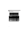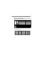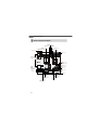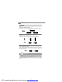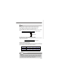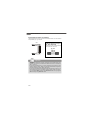
1
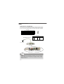
Fuzzy GM965/GME965
MS-9803 (V1.X) Mainboard
G52-98031X4
i
PDF created with pdfFactory Pro trial version www.pdffactory.com
Copyright Notice
Th e material in this d ocument is the in tellectual p rop erty of MICRO-STAR
INTERNATIONAL. We take every care in the preparation of this document, but no
guarantee is given as to the correctness of its contents. Our products are under
continual improvement and we reserve the right to make changes without notice.
Trademarks
All trademarks are the properties of their respective owners.
Intel® and Pentium® are registered trademarks of Intel Corporation.
AMD, Athlon™, Athlon™ XP, Thoroughbred™, and Duron™ are registered trademarks of AMD Corporation.
NVIDIA, the NVIDIA logo, DualNet, and nForce are registered trademarks or trademarks of NVIDIA Corporation in the United States and/or other countries.
PS/2 and OS ®/2 are registered trademarks of International Business Machines
Corporation.
Windows® 98/2000/NT/XP/Vista are registered trademarks of Microsoft Corporation.
Netware® is a registered trademark of Novell, Inc.
Award® is a registered trademark of Phoenix Technologies Ltd.
AMI® is a registered trademark of American Megatrends Inc.
Revision History
Revision
V1.3
Revision History
Updating the clear CMOS jumper
Date
December 2008
Technical Support
If a problem arises with your system and no solution can be obtained from the user’s
manual, please contact your place of purchase or local distributor. Alternatively,
please try the following help resources for further guidance.
Visit th e MSI web site at http://global.msi.com.tw/index.php?
func=service for FAQ, technical guide, BIOS updates, driver updates, and
other information.
Contact our technical staff at http://ocss.msi.com.tw.
ii
PDF created with pdfFactory Pro trial version www.pdffactory.com
Safety Instructions
1.
Always read the safety instructions carefully.
2.
Keep this User’s Manual for future reference.
3.
Keep this equipment away from humidity.
4.
Lay this equipment on a reliable flat surface before setting it up.
5.
The openings on the enclosure are for air convection hence protects the equipment from overheating. DO NOT COVER THE OPENINGS.
6.
Make sure the voltage of the power source and adjust properly 110/220V before connecting the equipment to the power inlet.
7.
Place the power cord such a way that people can not step on it. Do not place
anything over the power cord.
8.
Always Unplug the Power Cord before inserting any add-on card or module.
9.
All cautions and warnings on the equipment should be noted.
10. Never pour any liquid into the opening that could damage or cause electrical
shock.
11. If any of the following situations arises, get the equipment checked by service
personnel:
The power cord or plug is damaged.
Liquid has penetrated into the equipment.
The equipment has been exposed to moisture.
The equipment does not work well or you can not get it work according to
User’s Manual.
The equipment has dropped and damaged.
The equipment has obvious sign of breakage.
12. DO NOT LEAVE THIS EQUIPMENT IN AN ENVIRONMENT UNCONDITIONED, STORAGE TEMPERATURE ABOVE 600 C (1400F), IT MAY DAMAGE THE EQUIPMENT.
CAUTION: Danger of explosion if battery is incorrectly replaced.
Replace only with the same or equivalent type recommended by the
manufacturer.
iii
FCC-B Radio Frequency Interference Statement
Th is eq u ip men t h as been
tested and found to comply
with the limits for a Class B
digital device, pursuant to Part
15 of the FCC Rules. These limits are designed to provide reasonable protection
against harmful interference in a residential installation. This equipment generates,
uses and can radiate radio frequency energy and, if not installed and used in accordance with the instructions, may cause harmful interference to radio communications.
However, there is no guarantee that interference will not occur in a particular
installation. If this equipment does cause harmful interference to radio or television
reception, which can be determined by turning the equipment off and on, the user is
encouraged to try to correct the interference by one or more of the measures listed
bel ow.
Reorient or relocate the receiving antenna.
Increase the separation between the equipment and receiver.
Connect the equipment into an outlet on a circuit different from that to
which the receiver is connected.
Consult the dealer or an experienced radio/television technician for help.
Notice 1
The changes or modifications not expressly approved by the party responsible for
compliance could void the user’s authority to operate the equipment.
Notice 2
Shielded interface cables and A.C. power cord, if any, must be used in order to
comply with the emission limits.
VOIR LA NOTICE D’INSTALLATION AVANT DE RACCORDER AU RESEAU.
Micro-Star International
MS-9803
This device complies with Part 15 of the FCC Rules. Operation is subject to the
following two conditions:
(1) this device may not cause harmful interference, and
(2) this device must accept any interference received, including interference that
may cause undesired operation.
iv
WEEE (Waste Electrical and Electronic Equipment) Statement
v
vi
vii
CONTENTS
Copyright Notice .................................................................................................... ii
Trademarks ............................................................................................................ ii
Revision History .................................................................................................... ii
Technical Support ................................................................................................. ii
Safety Instructions ................................................................................................ iii
FCC-B Radio Frequency Interference Statement ................................................... iv
WEEE (Waste Electrical and Electronic Equipment) Statement ................................ v
Chapter 1 Product Overview .......................................................................... 1-1
Mainboard Specifications ............................................................................. 1-2
Block Diagram ............................................................................................... 1-4
Mainboard Layout ........................................................................................ 1-5
Board Dimension .......................................................................................... 1-6
Back Panel & I/O Shield Drawing .................................................................. 1-7
Power Consumption .................................................................................... 1-8
Safety Compliance & MTBF .......................................................................... 1-9
Chapter 2 Hardware Setup ............................................................................. 2-1
Quick Components Guide ............................................................................. 2-2
CPU (Central Processing Unit) ...................................................................... 2-3
Memory ....................................................................................................... 2-6
Power Supply .............................................................................................. 2-7
Back Panel ................................................................................................... 2-8
Connector .................................................................................................. 2-10
Jumper ...................................................................................................... 2-18
Slot ............................................................................................................ 2-19
Chapter 3 BIOS Setup ...................................................................................... 3-1
Entering Setup ............................................................................................. 3-2
The Menu Bar .............................................................................................. 3-4
Main ............................................................................................................. 3-5
Advanced .................................................................................................... 3-6
Boot ........................................................................................................... 3-17
Security ..................................................................................................... 3-21
Chipset ...................................................................................................... 3-22
Exit ............................................................................................................ 3-26
Chapter 4 System Resources ....................................................................... 4-1
Watch Dog Timer Setting .............................................................................. 4-2
AMI POST Code ........................................................................................... 4-3
Resource List .............................................................................................. 4-7
viii
Product Overview
Chapter 1
Product Overview
Thank you for choosing the Fuzzy GM965/GME965 (MS9803 v1.X) Mini ITX mainboard from MSI.
Based on the innovative Intel ® GM965/GME965 &
ICH8M controllers for optimal system efficiency, the
Fuzzy GM965/GME965 accommodates the latest Intel®
Core 2 Duo/Core Duo/Celeron M processors in
Socket P and supports two 240-pin 533/667MHz DDR2
DIMM slots to provide the maximum of 4GB memory
capacity.
In the entry-level and mid-range market segment, the
Fuzzy GM965/GME965 can provide a high-performance
solution for today’s front-end and general purpose
workstation, as well as in the future.
1-1
MS-9803 Mainboard
Mainboard Specifications
Processor
- Intel Core 2 Duo/Core Duo/Celeron M CPU in Socket P
- Supports 3-pin CPU fan pin-header with Fan Speed Control
- Supports Intel Dual Core Technology to 533/667/800MHz and up
Supported FSB
- 533/667/800MHz
Chipset
- North Bridge: Intel GM965/GME965 chipset
- South Bridge: Intel ICH8M chipset
M e mo ry
- DDR2 533/667 SDRAM (4GB Max)
- 2 DDR2 DIMM slots (240pin / 1.8V)
LAN
- Supports 2 Gb Ethernet by Intel 82573L & 82566DC
Audio
- HDA Codec by Realtek ALC888 7.1 channel
- Compliant with Azalia 1.0 specs
- 6 watt amplifier
IDE
- 1 IDE port by ICH8M
- Supports Ultra DMA 66/100 mode
- Supports PIO, Bus Master operation mode
SATA
- SATA II ports by ICH8M
- Supports two SATA II devices
- Supports storage and data transfers at up to 3Gb/s
Connectors
Back Panel
- 2 RJ-45 LAN jacks
- 4 USB 2.0 ports
- 1 D-Sub VGA connector
- 1 serial port
1-2
PDF created with pdfFactory Pro trial version www.pdffactory.com
Product Overview
- 1 PS2 keyboard/mouse port
- 6 audio jacks
Onboard Connectors
- 2 USB 2.0 connectors (4 ports)
- 1 parallel port connector
- 1 SPDIF connector
- 1 LVDS connector
- 1 TV-out connector
- 1 digital I/O connector (16GPIO)
- 1 serial port connector
- 1 front panel connector
- 1 amplifier connector (4-pin)
Slots
-
1 PCI Express x16 slot
1 Mini PCI-E slot
1 32-bit/33MHz PCI slot
1 CF socket (optional)
Form Factor
- M ini ITX: 170mm x 170mm
Mounting
- 4 mounting ho les
Environmental
Storage Environment
- Temperature: -20 oC ~ 80 o C
- Humidity: 0% RH ~ 95% RH
Operation Environment
- Temperature: 0 oC ~ 60 o C
- Humidity: 0% RH ~ 85% RH
1-3
PDF created with pdfFactory Pro trial version www.pdffactory.com
MS-9803 Mainboard
Block Diagram
1-4
Product Overview
Mainboard Layout
To p:
Mou se
Botto m:
Keyboa rd
J5
CPUFAN1
ATX1
SYSFAN1
Top: COM Port
Bottom: VGA Port
DIMM1
DIMM2
B ATT
+
JBAT1
Intel
GM965/GME965
IDE1
To p: LAN Jack
Bo ttom: USB Po rts
Inte l
T: Lin e-In
M: Lin e-Ou t 8256 6DC
B: Mi c
T: RS-Out
M: CS -Out
B: SPDIF Out
CON1
Intel
ICH8M
JCF_SEL1
( O p ti on a l)
JLPT1
JSPI2
JSPD 1
SATA1
JLVDS1
SATA2
JTV2
To p: L AN Jack
Bo tto m: USB Po rts
Inte l
8257 3L
PCI-E 1
F_U SB2
F_USB1
J7
COM2
JFP1
AL C888
J4
JLPC1
JAMP1
J6
JCASE1
PCI1
CF1
(O p ti o na l )
Fuzzy GM965/GME965 (MS-9803 v1.X) Mini ITX Mainboard
1-5
MS-9803 Mainboard
Board Dimension
1-6
Product Overview
Back Panel & I/O Shield Drawing
1-7
MS-9803 Mainboard
Power Consumption
Component
Description
CPU
Intel Core 2 Duo T7100 processor
Memory
Kingston 2G DDR2-667 x2
Add-On VGA
Nvidia FX1400 PCI-Express VGA Card x1
Hard Disk
Seagate 500G SATA2 7200rpm HDD x1
Operating system
Microsoft Windows XP Professional SP2
MS-9803
®
3.3V
5V
®
12V Main
5V Standby
Connector
12V
(-)12V
Current(A) Current(A) Current(A) Current(A) Current(A) Current(A)
Enter DOS(Stable)
Enter BIOS(Stable)
Idle
CPU Stress 100%
Windows stress(3dMARK2006)
Windows Desktop Standby S1
with/without two LANs connected
(stable)
Windows Desktop Standby S3
with/without two LANs connected
(stable)
Windows Desktop Hibernate S4
with/without two LANs connected
(stable)
Windows Desktop Soft Off S5
with/without two LANs connected
(stable)
1-8
2.45
2.42
1.64
1.66
1.66
1.08/1.07
2.75
2.74
2.37
2.7
3.22
1.78/1.76
2.97
2.97
1.92
3.5
4.5
1.58/1.56
0
0.05
0
0.05
0
0.05
0
0.05
0
0.05
0 0.08/0.080
0.02
0.02
0.01
0.02
0.02
0.02
0
0
0
0
0.45/0.44
0
0
0
0
0
0.25/0.24
0
0
0
0
0
0.25/0.24
0
Product Overview
Safety Compliance & MTBF
Standard number
Certification
CE
BSMI
CNS 13438 乙類(1997年版)
C-Tick
AS/NZS CISPR 22:2004
FCC
VCCI
Title of standard
EN 55022:1998+A1:2000+A2:2003 Class B Product family standard
Limits for harmonic current
EN 6100-3-2:2000 Class D
emission
RFI
Limitation of voltage
EN 6100-3-3:1995+A1:2001
fluctuation and flicker in lowvoltage supply system
Immunity EN 55024:1998+A1:2001+A2:2003
Product family standard
FCC CFR Title 47 Part 15 Subpart B: 2005 Class B
CISPR 22: 2005
VCCI V-3:2004, Class B
VCCI V-4:2004, Class B
MTBF - Reliability Prediction
Operation
Operating
temperature (℃)
Environment
Calculation Model
Duty Cycle
MTBF (hr.)
10,867.351095
92,019
117.312341
8,524
GF, GU - Ground Fixed,
Telcordia Issue 1
35
Uncontrolled
MIL-HDBK-217 FN2
55
GF, GU - Ground Fixed,
Uncontrolled
1-9
This page is intentionally left blank.
viii
Hardware Setup
Chapter 2
Hardware Setup
This chapter provides you with the information about
hardware setup procedures. While doing the installation,
be careful in holding the components and follow the
installation procedures. For some components, if you
install in the wrong orientation, the components will not
work properly.
Use a grounded wrist strap before handling computer
comp onen ts. Static el ectricity may damag e th e
components.
2-1
MS-9803 Mainboard
Quick Components Guide
CPUFAN1, p.2-13
JTV2, p.2-14
SYSFAN1,
p.2-13
JLVDS1, p.2-15
JBAT1,
p.2-18
DIMM Slots, p.2-6
CPU, p.2-3
J5, p.2-18
ATX1, p.2-7
Back Panel
I/O, p.2-8
IDE1, p.2-10
JCF_SEL1, p.2-20
SATA1/2, p.2-11
JLPT1, p.2-17
JSPI2, p.2-12
COM2, p.2-17
JSPD1, p.2-12
PCI-E Slot,
p.2-19
J4, p.2-11
JFP1, p.2-13
J6, p.2-18
F_USB1/2, p.2-16
PCI Slot, p.2-19
JCASE1, p.2-10
J7, p.2-18
JAMP1, p.2-12
2-2
Hardware Setup
CPU (Central Processing Unit)
The mainboard supports Intel ® Core 2 Duo/Core Duo/Celeron M processors in
Socket P. When you are installing the CPU, make sure the CPU has a heat sink
and a cooling fan attached on the top to prevent overheating. If you do not
have the heat sink and cooling fan, contact your dealer to purchase and install them
before turning on the computer.
Important
1. Overheating will seriously damage the CPU and system. Always make
sure the cooling fan can work properly to protect the CPU from overheating.
2. Make sure that you apply an even layer of heat sink paste (or thermal tape)
between the CPU and the heatsink to enhance heat dissipation.
3. While replacing the CPU, always turn off the power supply or unplug the
power supply’s power cord from the grounded outlet first to ensure the
safety of CPU.
2-3
MS-9803 Mainboard
CPU & Cooler Installation for Socket P
1. Lo cate th e C PU s ock et on t h e
mainboard.
2. Place the CPU on top of the socket. Make sure to align the gold arrow on the CPU
with the arrow key on the socket.
3. Push the CPU down until its pins securely fit into the socket.
4. On the front end of the CPU socket is a
locking mechanism designed into the
form of a screw head. Make sure that
you actuate or deactuate this mechanism with a screwdriver before and after installing the CPU.
Important
2-4
Hardware Setup
5. Flip over the mainboard and locate the position of the CPU socket.
6. Install the backplate to the back of the CPU socket with holes aligned.
CPU cooler backplate
7. The heatsink paste helps to enhance heat dissipation of the CPU. Before installing
the cooler set (fan & heatsink bundled), make sure that you detach the shield of
the heatsink paste under the cooler set.
8. Locate the four screw holes around the CPU socket where the CPU cooler
backplate was installed. Align the cooler set with the screw holes and mount it on
top of the CPU.
9. Screw to secure the cooler set to
the mainboard.
10. Connect the fan power cable to the
CPUFAN1 connector on the mainboard.
2-5
MS-9803 Mainboard
Memory
The DIMM slots are intended for system memory modules.
DDR2
240-pin, 1.8V
64x2=128 pin
56x2=112 pin
Installing DDR2 Modules
1. The memory module has only one notch on the center and will only fit in the right
orientation.
2. Insert the memory module vertically into the DIMM slot. Then push it in until the
golden finger on the memory module is deeply inserted in the DIMM slot.
Important
You can barely see the golden finger if the memory module is properly inserted
in the DIMM slot.
3. The plastic clip at each side of the DIMM slot will automatically close.
Volt
2-6
Notch
Hardware Setup
Power Supply
ATX 20-Pin System Power Connector: ATX1
This connector allows you to connect to an ATX power supply. To connect to the ATX
power supply, make sure the plug of the power supply is inserted in the proper
orientation and the pins are aligned. Then push down the power supply firmly into the
connector.
ATX1
20
10
11
1
ATX1 Pin Definition
PIN
SIGNAL
PIN
SIGNAL
1
2
3
4
5
6
7
8
9
3.3V
3.3V
GND
5V
GND
5V
GND
PW_OK
5V_SB
10
12V
11
12
13
14
15
16
17
18
19
20
3.3V
-12V
GND
PS_ON
GND
GND
GND
-5V
5V
5V
Important
Power supply of 350watts (and above) is highly recommended for system
stability.
2-7
MS-9803 Mainboard
Back Panel
Serial Port
LAN
LAN
M ouse
Line-In RS-Out
Line-Out CS-Out
VGA Port
Keyboard
USB Ports
USB Ports
MIC
Optical
SPDIF-Out
Mouse/Keyboard
The standard PS/2® mouse/keyboard DIN connector is for a PS/2® mouse/keyboard.
Serial Port
The serial port is a 16550A high speed communications port that sends/ receives 16
bytes FIFOs. You can attach a serial mouse or other serial devices directly to the
connector.
VGA Port
The DB15-pin female connector is provided for monitor.
USB Port
The USB (Universal Serial Bus) port is for attaching USB devices such as keyboard,
mouse, or other USB-compatible devices.
LAN
The standard RJ-45 LAN jack is for connection to the Local Area Network (LAN).
You can connect a network cable to it.
LED
Color
LED State
Off
Left
Green
On (steady state)
Activity Indicator
Link Indicator
Condition
LAN link is not established.
LAN link is established.
On (brighter & pulsing) The computer is communicating with another computer on the LAN.
Green
Off
10 Mbit/sec data rate is selected.
On
100 Mbit/sec data rate is selected.
Orange
On
1000 Mbit/sec data rate is selected.
Right
2-8
Hardware Setup
Audio Ports
These audio connectors are used for audio devices. You can differentiate the color
of the audio jacks for different audio sound effects.
Line-In (Blue) - Line In / Side-Surround Out in 7.1 channel mode, is used
for extern al CD player, tap epl ayer or oth er aud io
devices.
Line-Out (Green) - Line Out, is a connector for speakers or headphones.
Mic (Pink) - Mic, is a connector for microphones.
RS-Out (Black) - Rear-Surround Out in 4/ 5.1/ 7.1 channel mode.
CS-Out (Orange) - Center/ Subwoofer Out in 5.1/ 7.1 channel mode.
Optical S/PDIF-Out
This SPDIF (Sony & Philips Digital Interconnect Format) connector is provided for
digital audio transmission to external speakers through an optical fiber cable.
2-9
MS-9803 Mainboard
Connector
Chassis Intrusion Connector: JCASE1
This connector connects to the chassis intrusion switch cable. If the chassis is
opened, the chassis intrusion mechanism will be activated. The system will record
this status and show a warning message on the screen. To clear the warning, you
must enter the BIOS utility and clear the record.
GND
CINTRU
1
2
JCASE1
IDE Connector: IDE1
This connector supports IDE hard disk drives, optical disk drives and other IDE devices.
IDE1
Important
If you install two IDE devices on the same cable, you must configure the drives
separately to master / slave mode by setting jumpers. Refer to IDE device’s
documentation supplied by the vendors for jumper setting instructions.
2-10
Hardware Setup
Digital IO Connector: J4
The J4 is designed to connect the General-Purpose Input/Output (GPIO) peripheral
module.
Pin Definition
J4
19
20
1
2
PIN
SIGNAL
PIN
SIGNAL
1
3
5
7
9
11
13
15
17
19
VCC3
N_GPIO10
N_GPIO11
N_GPIO12
N_GPIO13
N_GPIO14
N_GPIO15
N_GPIO16
N_GPIO17
GND
2
4
6
8
10
12
14
16
18
20
VCC5
N_GPIO20
N_GPIO21
N_GPIO22
N_GPIO23
N_GPIO24
N_GPIO25
N_GPIO26
N_GPIO27
NC
Serial ATA II Connector: SATA1, SATA2
This connector is a high-speed Serial ATA II interface port. Each connector can
connect to one Serial ATA II device.
SATA2 SATA1
Important
Please do not fold the Serial ATA cable into 90-degree angle. Otherwise,
data loss may occur during transmission.
2-11
MS-9803 Mainboard
Audio Amplifier Connector: JAMP1
The JAMP1 is used to connect audio amplifiers to enhance audio performance.
Pin Definition
JAMP1
1
PIN
SIGNAL
1
AMP_L-
2
3
4
AMP_L+
AMP_RAMP_R+
S/PDIF-Out Connector: JSPD1 (Optional, for HDMI graphics card
only)
This connector is used to connect S/PDIF (Sony & Philips Digital Interconnect Format)
interface for digital audio transmission to the HDMI graphics card.
GND
SPDIF-Out
JSPD1
SPI Flash ROM Connector: JSPI2
This connector is used to flash SPI flash ROM.
JSPI2
9
10
1
2
Pin Definition
2-12
Pin
Description
Pin
Description
1
VCC3_SB
2
VCC3_SB
3
SPI_MISO_F
4
SPI_MOSI_F
5
SPI_CS0_F#
6
SPI_CLK_F
7
GND
8
GND
9
SPI_HOLD#
10
NC
Hardware Setup
Fan Power Connectors: CPUFAN1, SYSFAN1
The fan power connectors support system cooling fan with +12V. When connecting
the wire to the connectors, always note that the red wire is the positive and should
be connected to the +12V; the black wire is Ground and should be connected to GND.
If the mainboard has a System Hardware Monitor chipset on-board, you must use a
specially designed fan with speed sensor to take advantage of the CPU fan control.
SENSOR
GND
+1 2V
CPUFAN1,
SYSFAN1
Important
Please refer to the recommended CPU fans at Intel® official website or consult
the vendors for proper CPU cooling fan.
Front Panel Connector: JFP1
The mainboard provides one front panel connector for electrical connection to the
front panel switches and LEDs. The JFP1 is compliant with Intel® Front Panel I/O
Connectivity Design Guide.
JFP1
10
Power Switch +
Power
LED
2
9
1
+ Reset
- Switch
- HDD
+ LED
JFP1 Pin Definition
PIN
SIGNAL
DESCRIPTION
1
2
3
4
5
6
7
8
9
HD_LED +
FP PWR/SLP
HD_LED FP PWR/SLP
RST_SW PWR_SW +
RST_SW +
PWR_SW RSVD_DNU
Hard disk LED pull-up
MSG LED pull-up
Hard disk active LED
MSG LED pull-up
Reset Switch low reference pull-down to GND
Power Switch high reference pull-up
Reset Switch high reference pull-up
Power Switch low reference pull-down to GND
Reserved. Do not use.
2-13
MS-9803 Mainboard
TV-Out Connector: JTV2 (Optional)
This connector is for you to attach an optional TV-Out bracket that offers two types
of TV-Out connectors: S-Video and RCA Composite connectors. Select the appropriate one to connect the standard television or the HDTV (High-Definition TeleVision).
Display Matrix
CRT
CRT
LVDS
TV-OUT
SDVO
PCI-E x16 port
LVDS
TV-OUT SDVO
V
V
V
V
X
V
V
V
V
X
V
X
V : Support
V
V
V
PCI-E x16
port
X
X
X
X
3
2
1
5
4
JTV2
X
X : No Support
Pin Definition
TV-Out Bracket (Optional)
Pin
Description
Pin
Description
1
GND
4
GND
2
LCVBS
5
LC
3
LY
6
NC
Connect to JTV2
Standard TV-Out
HDTV-Out Connector
(RCA Composite) Connector (S-Video)
Important
Please note that the TV-Out bracket can connect to one TV only. Users have
to choose either the RCA Composite or the S-Video to connect. Simultaneously connecting two TVs to this bracket is prohibited and may lead to the
malfunction of the TVs.
2-14
Hardware Setup
LVDS Flat Panel Connector: JLVDS1
The LVDS (Low Voltage Differential Signal) connector provides a digital interface
typically used with flat panels. After connecting an LVDS interfaced flat panel to the
JLVDS1, be sure to check the panel datasheet and set the J7 LVDS Power Selection Jumper (p. 2-18) to a proper voltage.
Display Matrix
JLVDS1
CRT
1
39
2
40
CRT
LVDS
TV-OUT
SDVO
PCI-E x16 port
LVDS
TV-OUT SDVO
V
V
V
V
X
V
V
V
V
X
V
X
V : Support
SIGNAL
PIN
V
V
V
PCI-E x16
port
X
X
X
X
X
X : No Support
SIGNAL
+12V
2
1
+12V
+12V
4
3
+12V
GND
6
5
+12V
GND
8
7
VCC3/VCC5
LCD_VDD
10
9
LCD_VDD
LDDC_DATA
12
11
LDDC_CLK
LVDS_VDDEN
14
13
L_BKLTCTL
GND
16
15
L_BKLTEN
LA_DATA0
18
17
LA_DATA0#
LA_DATA1
20
19
LA_DATA1#
LA_DATA2
22
21
LA_DATA2#
LA_CLK
24
23
LA_CLK#
LA_DATA3
26
25
LA_DATA3#
GND
28
27
GND
LB_DATA0
30
29
LB_DATA0#
LB_DATA1
32
31
LB_DATA1#
LB_DATA2
34
33
LB_DATA2#
LB_CLK
36
35
LB_CLK#
LB_DATA3
38
37
LB_DATA3#
GND
40
39
GND
2-15
MS-9803 Mainboard
Front USB Connector: F_USB1, F_USB2
This connector, compliant with Intel® I/O Connectivity Design Guide, is ideal for connecting high-speed USB interface peripherals such as USB HDD, digital cameras,
MP3 players, printers, modems and the like.
Pin Definition
1
2
9
10
F_USB1/2
PIN
SIGNAL
PIN
SIGNAL
1
VCC
2
VCC
3
USB0-
4
USB1-
5
USB0+
6
USB1+
7
GND
8
GND
9
Key (no pin)
10
NC
USB 2.0 Bracket
(Optional)
Important
Note that the pins of VCC and GND must be connected correctly to avoid
possible damage.
2-16
Hardware Setup
Serial Port Connector: COM 2
This connector is a 16550A high speed communications port that sends/receives 16
bytes FIFOs. You can attach a serial device to it through the optional serial port
bracket.
Pin Definition
PIN
2
1
10
9
1
2
3
4
5
6
7
8
9
COM2
SIGNAL
DESCRIPTION
DCD
SIN
SOUT
DTR
GND
DSR
RTS
CTS
VCC_COM3
Data Carry Detect
Serial In or Receive Data
Serial Out or Transmit Data
Data Terminal Ready
Ground
Data Set Ready
Request To Send
Clear To Send
Power Source
Parallel Port Connector: JLPT1
The mainboard provides a 26-pin header for connection to an optional parallel port
bracket. The parallel port is a standard printer port that supports Enhanced Parallel
Port (EPP) and Extended Capabilities Parallel Port (ECP) mode.
JLPT1
25
26
1
2
Pin
Signal Name
Pin
Signal Name
1
RSTB#
2
AFD#
3
PRND0
4
ERR#
5
PRND1
6
PINIT#
7
PRND2
8
LPT_SLIN#
9
PRND3
10
GND
11
PRND4
12
GND
13
PRND5
14
GND
15
PRND6
16
GND
17
PRND7
18
GND
19
ACK#
20
GND
21
BUSY
22
GND
23
PE
24
GND
25
SLCT
26
GND
Parallel/Serial Port Bracket (Optional)
2-17
MS-9803 Mainboard
Jumper
LVDS Power Selection Jumper: J7
Use this jumper to specify the operation voltage of the LVDS interfaced flat panel.
1
1
+3V
J7
1
1
+5V
+12V
COM Port Power Jumpers: J5, J6
These jumpers specify the operation voltage of the onboard serial ports.
1
1
1
1
J5
+5V
+12V
1
1
J6
+12V
+5V
Clear CMOS Jumper: JBAT1
There is a CMOS RAM onboard that has a power supply from external battery to keep
the data of system configuration. With the CMOS RAM, the system can automatically
boot OS every time it is turned on. If you want to clear the system configuration, set
this jumper to clear data.
1
JBAT1
3
1
Keep Data
1
3
Clear Data
Important
You can clear CMOS by shorting 2-3 pin while the system is off. Then return
to 1-2 pin position. Avoid clearing the CMOS while the system is on; it will
damage the mainboard.
2-18
PDF created with pdfFactory Pro trial version www.pdffactory.com
Hardware Setup
Slot
PCI (Peripheral Component Interconnect) Express Slot
The PCI Express slot supports PCI Express interface expansion cards.
The PCI Express x 16 slot supports up to 4.0 GB/s transfer rate.
The CON1 is Mini PCI-E connector for wireless LAN, TV tuner, and Robson NAND
Flash.
PCI Express x16 Slot
Mini PCI-E Slot
PCI (Peripheral Component Interconnect) Slot
The PCI slot supports LAN card, SCSI card, USB card, and other add-on cards that
comply with PCI specifications.
32-bit PCI Slot
PCI Interrupt Request Routing
The IRQ, acronym of interrupt request line and pronounced I-R-Q, are hardware lines
over which devices can send interrupt signals to the microprocessor. The PCI IRQ
pins are typically connected to the PCI bus pins as follows:
DEVICE
INT Pin
IDSEL
CLOCK
REQ# / GNT#
32-bit PCI Slot
PIRQA
AD17
PCICLK 0
REQ#0 / GNT#0
32-bit PCI Riser
PIRQC
AD18
PCICLK 1
REQ#1 / GNT#1
32-bit PCI Riser
PIRQD
AD19
PCICLK 2
REQ#2 / GNT#2
Important
When adding or removing expansion cards, make sure that you unplug the
power supply first. Meanwhile, read the documentation for the expansion card
to configure any necessary hardware or software settings for the expansion
card, such as jumpers, switches or BIOS configuration.
2-19
MS-9803 Mainboard
CompactFlash Card Slot: CF1 (Optional)
This CompactFlash slot shares one channel of the IDE controller. You can install one
CompactFlash typeI / type II device.
CF1
CF Mode Selecting Jumper:
JCF_SEL1 (Optional)
This jumper is used to select Master/
Slave mode of the CF device.
JCF_SEL1
1
1
1
Master
Slave
Important
* The CF1 slot and the IDE1 connector shares and uses the same channel. CF1
and IDE1 can support up to 2 IDE devices without CF device or 1 IDE device
with 1 CF device.
* If you install two IDE devices, you must configure the second drive to Slave
mode by setting its jumper. Refer to the hard disk documentation supplied by
hard disk vendors for jumper setting instructions.
* If you install one IDE device with ATA133 IDE cable and one CF device, you
must configure the CF drive to Master mode by setting jumper JCF_SEL1.
CF only supports Master mode by using ATA133 IDE cable. CF only supports
Slave mode by using ATA33 IDE cable.
2-20
BIOS Setup
Chapter 3
BIOS Setup
This chapter provides information on the BIOS Setup
program and allows you to configure the system for
optimum use.
You may need to run the Setup program when:
² An error message appears on the screen during the
system booting up, and requests you to run SETUP.
² You want to change the default settings for customized features.
3-1
MS-9803 Mainboard
Entering Setup
Power on the computer and the system will start POST (Power On Self Test) process.
When the message below appears on the screen, press <Del> key to enter Setup.
Press Del to enter SETUP
If the message disappears before you respond and you still wish to enter Setup,
restart the system by turning it OFF and On or pressing the RESET button. You may
also restart the system by simultaneously pressing <Ctrl>, <Alt>, and <Delete> keys.
Important
1. The items under each BIOS category described in this chapter are under
continuous update for better system performance. Therefore, the description may be slightly different from the latest BIOS and should be held for
reference only.
2. Upon boot-up, the 1st line appearing after the memory count is the BIOS
version. It is usually in the format:
A9803IMS V1.0 041507 where:
1st digit refers to BIOS maker as A = AMI, W = AWARD, and P =
PHOENIX.
2nd - 5th digit refers to the model number.
6th digit refers to the chipset as I = Intel, N = nVidia, and V = VIA.
7th - 8th digit refers to the customer as MS = all standard customers.
V1.0 refers to the BIOS version.
041507 refers to the date this BIOS was released.
3-2
BIOS Setup
Control Keys
<↑>
<↓>
<←>
<→>
<Enter>
<Esc>
<+/PU>
<-/PD>
<F6>
<F7>
<F10>
Move to the previous item
Move to the next item
Move to the item in the left hand
Move to the item in the right hand
Select the item
Jumps to the Exit menu or returns to the main menu from a
submenu
Increase the numeric value or make changes
Decrease the numeric value or make changes
Load Optimized Defaults
Load Fail-Safe Defaults
Save all the CMOS changes and exit
Getting Help
After entering the Setup menu, the first menu you will see is the Main Menu.
Main Menu
The main menu lists the setup functions you can make changes to. You can use the
arrow keys ( ↑↓ ) to select the item. The on-line description of the highlighted setup
function is displayed at the bottom of the screen.
Sub-Menu
If you find a right pointer symbol (as shown in the right view) appears to the left of
certain fields that means a sub-menu can be launched from this
field. A sub-menu contains additional options for a field parameter.
You can use arrow keys ( ↑↓ ) to highlight the field and press
<Enter> to call up the sub-menu. Then you can use the control keys to enter values
and move from field to field within a sub-menu. If you want to return to the main
menu, just press the <Esc >.
General Help <F1>
The BIOS setup program provides a General Help screen. You can call up this screen
from any menu by simply pressing <F1>. The Help screen lists the appropriate keys
to use and the possible selections for the highlighted item. Press <Esc> to exit the
Help screen.
3-3
MS-9803 Mainboard
The Menu Bar
Main
Use this menu for basic system configurations, such as time, date etc.
Advanced
Use this menu to set up the items of special enhanced features.
Boot
Use this menu to specify the priority of boot devices.
Security
Use this menu to set supervisor and user passwords.
Chipset
This menu controls the advanced features of the onboard Northbridge and Southbridge.
Exit
This menu allows you to load the BIOS default values or factory default settings into
the BIOS and exit the BIOS setup utility with or without changes.
3-4
BIOS Setup
Main
AMI BIOS, Processor, System Memory
These items show the firmware and hardware specifications of your system. Read
only.
System Time
The time format is <Hour> <Minute> <Second>.
System Date
The date format is <Day>, <Month> <Date> <Year>.
3-5
MS-9803 Mainboard
Advanced
CPU Configuration
These items show the advanced specifications of your CPU. Read only.
3-6
BIOS Setup
IDE Configuration
ATA/IDE Configuration
This setting specifies the modes of the PATA & SATA ports.
Configure SATA as
s
This setting specifies the function of the on-chip SATA controller.
3-7
MS-9803 Mainboard
Primary/Secondary/Third/Fourth IDE Master/Slave
[Type]
Press PgUp/<+> or PgDn/<-> to select
[Manual], [None] or [Auto] type. Note that the
specifications of your drive must match with
the drive table. The hard disk will not work
properly if you enter improper information for
this category. If your hard disk drive type is
not matched or listed, you can use [Manual] to
define your own drive type manually.
[LBA/Large Mode]
Enabling LBA causes Logical Block Addressing to be used in place of Cylinders,
Heads and Sectors
[Block(Multi-Sector Transfer)] Any selection except Disabled determines
the number of sectors transferred per block
[PIO Mode]
Indicates the type of PIO (Programmed Input/
Output)
[DMA Mode]
Indicates the type of Ultra DMA
[S.M.A.R.T.]
This allows you to activate the S.M.A.R.T.
(Self-Monitoring Analysis & Reporting
Technology) capability for the hard disks. S.
M.A.R.T is a utility that monitors your disk sta
tus to predict hard disk failure. This gives you
an opportunity to move data from a hard disk
that is going to fail to a safe place before the
hard disk becomes offline.
[32 Bit Data Transfer]
Enables 32-bit communication between
CPU and IDE card
3-8
BIOS Setup
Super IO Configuration
Serial Port 1 / 2 Address
Select an address and a corresponding interrupt for the serial port 1/2.
Parallel Port Address
This setting specifies the I/O port address and IRQ of the onboard parallel port.
Chassis Intrusion
The field enables or disables the feature of recording the chassis intrusion
status and issuing a warning message if the chassis is once opened. To clear
the warning message, set the field to [Reset]. The setting of the field will
automatically return to [Enabled] later.
3-9
MS-9803 Mainboard
Hardware Health Configuration
System 1 / 2 Temperature, CPU Temperature, CPUFAN Speed, Vcore,
AVCC, 3VCC, +12V, 5V, VSB, VBAT
These items display the current status of all of the monitored hardware devices/components such as CPU voltage, temperatures and all fans’ speeds.
CPUFAN0 / CPUFAN1 Mode Setting
These settings specify the operation mode of the CPU fans.
CPUFAN0 / CPUFAN1 PWM Control
These settings control the PWM duty cycle of the CPU fans.
3-10
BIOS Setup
ACPI Configuration
Suspend Mode
This item specifies the power saving modes for ACPI function. If your operating
system supports ACPI, you can choose to enter the Standby mode in S1 (POS)
or S3 (STR) fashion through the setting of this field. Options are:
[S1 (POS)]
The S1 sleep mode is a low power state. In this state,
no system context is lost (CPU or chipset) and hardware maintains all system context.
[S3 (STR)]
The S3 sleep mode is a lower power state where the
information of system configuration and open applications/files is saved to main memory that remains
powered while most other hardware components turn
off to save energy. The information stored in memory
will be used to restore the system when a “wake up”
event occurs.
USB Device Wakeup from S3/S4
This setting allows the activity of the USB device to wake up the system from
S3/S4 sleep state.
3-11
MS-9803 Mainboard
APM Configuration
Power M anagement/APM
Setting to [Enabled] will activate an Advanced Power Management (APM) device to enhance Max Saving mode and stop CPU internal clock.
Power Button Mode
This setting controls the operation of the power button.
Resume On LAN
This field specifies whether the system will be awakened from power saving
modes when activity or input signal of onboard LAN is detected.
Resume On PME#
When setting to [Enabled], this setting allows your system to be awakened from
the power saving modes through any event on PME (Power Management Event).
Resume On RTC Alarm
When [Enabled], your can set the date and time at which the RTC (real-time
clock) alarm awakens the system from suspend mode.
3-12
BIOS Setup
Intel Robson Configuration
Intel Robson
Robson is the code name for a new Intel platform technology that uses nonvolatile memory (Flash memory) to increase system responsiveness, make
multi-tasking faster, and extend battery life. Intel Robson technology is poised
to eliminate many of the bottlenecks associated with HDD latency. By enabling
the majority of application workload to be written and read from a system cache
instead of the HDD, Robson will offer users of mobile computers built on the
Santa Rosa platform significantly increased performance -- particularly in application load and run time, the speed in which systems resume operation after
hibernation or boot, and in system-level power usage.
3-13
MS-9803 Mainboard
MPS Configuration
MPS Revision
This field allows you to select which MPS (Multi-Processor Specification) version to be used for the operating system. You need to select the MPS version
supported by your operating system. To find out which version to use, consult
the vendor of your operating system.
3-14
BIOS Setup
Trusted Computing
TCG/TPM Support
This setting controls the Trusted Platform Module (TPM) designed by the Trusted
Computing Group (TCG). TPMs are special-purpose integrated circuits (ICs)
built into a variety of platforms to enable strong user authentication and machine
attestation—essential to prevent inappropriate access to confidential and sensitive information and to protect against compromised networks.
3-15
MS-9803 Mainboard
USB Configuration
Legacy USB Support
Set to [Enabled] if you need to use any USB 1.1/2.0 device in the operating
system that does not support or have any USB 1.1/2.0 driver installed, such as
DOS and SCO Unix.
USB 2.0 Controller Mode
This setting specifies the operation mode of the onboard USB 2.0 controller.
Hotplug USB FDD Support
Set to [Enabled] if your need to use a hotplug USB-interfaced FDD in the operating system that does not support or have any USB driver installed, such as DOS
and SCO Unix.
3-16
BIOS Setup
Boot
Boot Settings Configuration
3-17
MS-9803 Mainboard
Quick Boot
Enabling this setting will cause the BIOS power-on self test routine to skip some
of its tests during bootup for faster system boot.
Quiet Boot
This BIOS feature determines if the BIOS should hide the normal POST messages with the motherboard or system manufacturer's full-screen logo.
When it is enabled, the BIOS will display the full-screen logo during the boot-up
sequence, hiding normal POST messages.
When it is disabled, the BIOS will display the normal POST messages, instead of
the full-screen logo.
Please note that enabling this BIOS feature often adds 2-3 seconds of delay to
the booting sequence. This delay ensures that the logo is displayed for a
sufficient amount of time. Therefore, it is recommended that you disable this
BIOS feature for a faster boot-up time.
AddOn ROM Display Mode
This item is used to determine the display mode when an optional ROM is
initialized during POST. When set to [Force BIOS], the display mode used by AMI
BIOS is used. Select [Keep Current] if you want to use the display mode of
optional ROM.
Bootup Num-Lock
This setting is to set the Num Lock status when the system is powered on.
Setting to [On] will turn on the Num Lock key when the system is powered on.
Setting to [Off] will allow users to use the arrow keys on the numeric keypad.
PS/2 Mouse Support
Select [Enabled] if you need to use a PS/2-interfaced mouse in the operating
system.
Wait For ‘F1’ If Error
When this setting is set to [Enabled] and the boot sequence encounters an
error, it asks you to press F1. If disabled, the system continues to boot without
waiting for you to press any keys.
Hit ‘DEL’ Message Display
Set this option to [Disabled] to prevent the message as follows:
Hit Del if you want to run setup
It will prevent the message from appearing on the first BIOS screen when the
computer boots. Set it to [Enabled] when you want to run the BIOS Setup Utility.
Interrupt 19 Capture
Interrupt 19 is the software interrupt that handles the boot disk function. When
enabled, this BIOS feature allows the ROM BIOS of these host adaptors to
"capture" Interrupt 19 during the boot process so that drives attached to these
adaptors can function as bootable disks. In addition, it allows you to gain access to the host adaptor's ROM setup utility, if one is available.
When disabled, the ROM BIOS of these host adaptors will not be able to "cap-
3-18
BIOS Setup
ture" Interrupt 19. Therefore, you will not be able to boot operating systems
from any bootable disks attached to these host adaptors. Nor will you be able to
gain access to their ROM setup utilities.
Boot Device Priority
1st Boot Device
The items allow you to set the sequence of boot devices where BIOS attempts
to load the disk operating system. First press <Enter> to enter the sub-menu.
Then you may use the arrow keys ( ↑↓ ) to select the desired device, then
press <+>, <-> or <PageUp>, <PageDown> key to move it up/down in the
priority list.
3-19
MS-9803 Mainboard
Removable Drives
1st Drive
This setting allows users to set the priority of the removable devices. First
press <Enter> to enter the sub-menu. Then you may use the arrow keys ( ↑↓ )
to select the desired device, then press <+>, <-> or <PageUp>, <PageDown>
key to move it up/down in the priority list.
3-20
BIOS Setup
Security
Supervisor Password / Change Supervisor Password
Supervisor Password controls access to the BIOS Setup utility. These settings allow
you to set or change the supervisor password.
User Password / Change User Password
User Password controls access to the system at boot. These settings allow you to
set or change the user password.
3-21
MS-9803 Mainboard
Chipset
3-22
BIOS Setup
North Bridge Configuration
Boot Graphics Adapter Priority
This item specifies which VGA card is your primary graphics adapter.
Internal Graphics Mode Select
The field specifies the size of system memory allocated for video memory.
PEG Port
This setting allows you to select whether to use the onchip graphics processor
or the PCI Express card. When set to [Auto], the BIOS checks to see if a PCI
Express graphics card is installed. If it detects that a PCI Express graphics card
is present, the motherboard boots up using that card. Otherwise, it defaults to
the onboard graphics processor.
PEG Force X1
This BIOS feature allows you to convert a PCI Express X16 slot into a PCI
Express X1 slot. When [Enabled], the PCI Express X16 slot will be forced to run
in the PCI Express X1 mode. When [Disabled], the PCI Express X16 slot will be
allowed to run in its normal PCI Express X16 mode.
If you have a PCI Express X16 graphics card installed in your system, you
should disable this BIOS feature. This allows for optimal performance of the
card by ensuring maximum transfer rates between the graphics card and the
motherboard.
But if you need to install a PCI Express X1 card into the PCI Express X16 slot,
you should enable this BIOS feature to ensure maximum compatibility.
3-23
MS-9803 Mainboard
Video Function Configuration
DVMT Mode Select
Intel's Dynamic Video Memory Technology (DVMT) allows the system to dynamically allocate memory resources according to the demands of the system at any point in time. The key idea in DVMT is to improve the efficiency of
the memory allocated to either system or graphics processor.
It is recommended that you set this BIOS feature to DVMT Mode for maximum
performance. Setting it to DVMT Mode ensures that system memory is dynamically allocated for optimal balance between graphics and system
performance.
DVMT/FIXED Memory
When set to DVMT/FIXED Mode, the graphics driver will allocate a fixed
amount of memory as dedicated graphics memory, as well as allow more
system memory to be dynamically allocated between the graphics processor and the operating system.
Boot Display Device
Use the field to select the type of device you want to use as the display(s)
of the system.
Boot Display Preferences
This setting allows you to set your preferences for the boot display device.
3-24
BIOS Setup
South Bridge Configuration
USB Functions
This setting specifies the function of the onboard USB controller.
USB 2.0 Controller
Set to [Enabled] if you need to use any USB 2.0 device in the operating system
that does not support or have any USB 2.0 driver installed, such as DOS and
SCO Unix.
GbE Controller
This setting disables/enables the onboard Gigabit Ethernet controller.
GbE LAN Boot
When [Enabled], the BIOS attempts to boot from a LAN boot image before it
attempts to boot from a local storage device.
GbE Wake Up From S5
This field specifies whether the system will be awakened from the S5 power
saving mode when activity or input signal of onboard LAN is detected.
HDA Controller
This setting controls the High Definition Audio interface integrated in the
Southbridge.
3-25
MS-9803 Mainboard
Exit
Save Changes and Exit
Save changes to CMOS and exit the Setup Utility.
Discard Changes and Exit
Abandon all changes and exit the Setup Utility.
Discard Changes
Abandon all changes and continue with the Setup Utility.
Load Optimal Defaults
Use this menu to load the default values set by the mainboard manufacturer specifically for optimal performance of the mainboard.
Load Failsafe Defaults
Use this menu to load the default values set by the BIOS vendor for stable system
performance.
3-26
System Resources
Chapter 4
System Resources
This chapter provides information on the following
system resources:
1. Watch Dog Timer Setting (p.4-2);
2. AMI POST Code (p.4-3);
3. Resource List (p.4-7).
4-1
MS-9803 Mainboard
Watch Dog Timer Setting
Software code
SIO_IDX equ 2EH
SIO_DTA equ 2FH
Timer equ 10; reset after 10 seconds
1. Enter configuration mode
mov dx,SIO_IDX
mov al,87h
out dx,al
out dx,al
2. Set to LDN 08
mov dx,SIO_IDX
mov al,07h
out dx,al
mov dx,SIO_DTA
mov al,08h
out dx,al
3. Set WatchDog Timer
mov dx,SIO_IDX
mov al,0f6h
out dx,al
mov dx,SIO_DTA
mov al,Timer
out dx,al
4. Exit configuration mode
mov dx,SIO_IDX
mov al,0AAh
out dx,al
4-2
System Resources
AMI POST Code
4-3
MS-9803 Mainboard
4-4
System Resources
4-5
MS-9803 Mainboard
4-6
System Resources
Resource List
Generic I/O Ports
(I) ICH8M GPIO
Pin
GPIO
Typ
Multi
Power
Connection.
AG12
0
I/O
BMBUSY#
3.3v
PM_BMBUSY#
AG22
11
I/O
SMBALERT#
3.3v
SMB_ALERT#
AE20
15
I/OD
STP_PCI#
3.3v
PM_STP_PCI#
AG18
3
I/OD
STP_CPU#
5v
PM_STP_CPU#
AH11
32
I/OD
CLKRUN#
3.3v
P_CLKRUN#
AJ8
1
I/OD
TACH1
3.3v
NC
AJ9
6
I/O
TACH2
3.3v
NC
AH9
7
I/O
TACH3
3.3v
NC
AE16
8
I/O
GPIO8
3.3v
SIO_PME#
AC19
12
I/O
GPIO12
3.3v
SPI_HOLD_GPO#
AG8
17
I/O
TACH0
3.3v
SPI_WP#
AH12
18
I/O
GPIO18
3.3v
SLPBTIN#
AE11
20
I/O
GPIO20
3.3v
ATADET0
AG10
22
I/O
SCLOCK
3.3v
NC
AH25
27
I/O
QRT_STATE0
3.3v
EL_STATE0
AD16
28
I/O
QRT_STATE1
3.3v
EL_STATE1
AG13
35
I/O
SATACLKREQ#
3.3v
CLK_SATA_OE#
AF9
38
I/O
SLOAD
3.3v
NC
AJ11
39
I/O
SDATAOUT0
3.3v
NC
AD10
48
I/O
SDATAOUT1
3.3v
NC
AJ12
21
I/O
SATA0GP
3.3v
RESISTOR
AJ10
19
I/O
SATA1GP
3.3v
RESISTOR
AF11
36
I/O
SATA2GP
3.3v
RESISTOR
AG11
37
I/O
SATA3GP
3.3v
RESISTOR
AH27
26
I/O
S4_STATE#
3.3v
NC
AJ27
24
I/O
NCMEM_LED
3.3v
LAN_EN
AJ24
10
I/O
ME_EC_ALERT
3.3v
PHY_DIS#
AF22
14
I/O
EC_ME_ALERT
3.3v
NC
AG19
9
I/O
WOL_EN
3.3v
NC
AG16
40
I/O
OC1#
3.3v
OC0#
AG15
41
I/O
OC2#
3.3v
OC0#
AE15
42
I/O
OC3#
3.3v
OC0#
AF15
43
I/O
OC4#
3.3v
OC1#
AG17
29
I/O
OC5#
3.3v
OC1#
AD12
30
I/O
OC6#
3.3v
OC1#
AJ18
31
I/O
OC7#
3.3v
OC1#
4-7
MS-9803 Mainboard
(Ⅱ) SIO GPIO
4-8
Pin
GPIO
Typ
Multi
Power
Connection.
121
17
I/O
VID7
VCC5
NC
122
16
I/O
VID6
VCC5
NC
123
15
I/O
VID5
VCC5
NC
124
14
I/O
VID4
VCC5
NC
125
13
I/O
VID3
VCC5
NC
126
12
I/O
VID2
VCC5
NC
127
11
I/O
VID1
VCC5
NC
128
10
I/O
VID0
VCC5
NC
120
20
O
CPUFANOUT1/GP20
VCC
CFAN_PWM
119
21
I/O
CPUFANN1/GP21
VCC
CPU_FAN
89
33
I/O
RSTOUT3#/GP33/SDA
VSB
NC
90
32
I/O
RSTOUT2#/GP32/SCL
VSB
NC
91
31
I/O
GP31
VSB
NC
92
30
I/O
GP30
VSB
NC
67
57
O
GP57/PSOUT#
VSB
PWRBTN#
68
56
I
GP56/PSIN#
VSB
IO_PWRBTN#
64
37
I/O
GP37
VSB
NC
72
53
I/O
GP53/PSON#
VSB
PS_ON#
73
52
I
GP52/SUSB#
VSB
SLP_S3#
77
50
I/O
WDTO#GP50
VSB
GP50
2
23
I/O
SCK/GP23
VCC
NC
88
34
O
RSTOUT4#GP34
VSB
NC
69
36
I/O
GP36
VSB
NC
87
35
I/O
GP35
VSB
NC
75
51
O
RSMRST#
VSB
VCC3
56
61
I
DCDA#
VCC
DCDA#
50
66
I
DDSRA#
VCC
DDSRA#
53
63
I
SINA
VCC
SINA
51
65
I/O
RTSA#
VCC
RTSA#
54
62
O
SOUTA
VCC
SOUTA
49
67
I
CTSA#
VCC
CTSA#
52
64
O
DTRA#
VCC
DTRA#
57
60
I
RIA#
VSB
RIA#
84
41
I
DCDB#
VSB
DCDB#
System Resources
79
46
I
DSRB#
VSB
DSRB#
82
43
I
SINB
VSB
SINB
80
45
O
RTSB#
VSB
RTSB#
83
42
O
SOUTB
VSB
SOUTB
78
47
I
CTSB#
VSB
CTSB#
81
44
O
DTRB#
VSB
DTRB#
85
40
I
RIB#
VSB
RIB#
63
26
I/O
KBDAT#
VSB
KBDAT#
62
27
I/O
KBCLK#
VSB
KBCLK#
66
24
I/O
MSDAT#
VSB
MSDAT#
65
25
I/O
MSCLK#
VSB
MSCLK#
70
55
I/O
SUSLED
VSB
GND
71
54
I/O
PWROK
VSB
NC
4-9
MS-9803 Mainboard
I/O Map
I /O P ort
0000-000F
0020-0021
002E-002F
0040-0043
004E-004F
0060, 0064
0070-0073
0080-0090
0092
00A0-00A1
00B2-00B3
00C0-00DF
00F0-00FF
01F0-01F7
02F8-02FF
0376
0378-037F
03F6
03F8-03FF
0400-045F
0500-050F
0CF8-0CFF
4-10
D es cription
DMA Controller 1
Interrupt Controller 1
SIO Port
System Timer
TPM Port
Keyboard Controller
RTC and CMOS
DMA Controller Page Registers
Port 92h
Interrupt Controller 2
APM Register
DMA Controller 2
Numeric Data Processor
Primary IDE Controller
COM2
Secondary IDE Controller
LPT1
Primary IDE Controller
COM1
ACPI I/O Space
SMBus I/O Space
PCI Configuration Port
System Resources
PCI Devices
PCI Device
Device
Host Bridge
VGA-compatible Controller
Other Display Controller
Ethernet Controller
UHCI USB Controller
UHCI USB Controller
Unknown Device
Unknown Device
PCI-to-PCI Bridge
UHCI USB Controller
UHCI USB Controller
UHCI USB Controller
Unknown Device
Subtractive Decode P2P Bridge
ISA Bridge
IDE Controller
IDE Controller
Smbus
Ven. ID Dev. ID
8086
2A00
8086
2A02
8086
2A03
8086
104B
8086
2834
8086
2835
8086
283A
8086
284B
8086
283F
8086
2830
8086
2831
8086
2832
8086
2836
8086
2448
8086
2815
8086
2850
8086
2828
8086
283E
Bus#
00
00
00
00
00
00
00
00
00
00
00
00
00
00
00
00
00
00
Dev#
00
02
02
19
1A
1A
1A
1B
1C
1D
1D
1D
1D
1E
1F
1F
1F
1F
Func#
00
00
01
00
00
01
07
00
00
00
01
02
07
00
00
01
02
03
4-11
MS-9803 Mainboard
SMBus Resource Allocation
SMBus Resource Allocation
Device
Address
Description
MS-7
0101 111X MSI ACPI Controller
DIMM Slot 1010 0000 SPD
ISA Interrupt Allocation
ISA Interrupt Allocation
IRQ
Description
IRQ0
System Timer
IRQ1
Keyboard Controller
IRQ2
Cascade Interrupt
IRQ3
COM2
IRQ4
COM1
IRQ5
PCI Device
IRQ6
PCI Device
IRQ7
LPT1
IRQ8
RTC
IRQ9
ACPI Controller Interrupt
IRQ10 PCI Device
IRQ11 PCI Device
IRQ12 PS/2 Mouse
IRQ13 Numeric Data Processor
IRQ14 Primary IDE Controller
IRQ15 Secondary IDE Controller
ISA DMA Channel Allocation
4-12