1
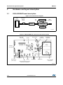
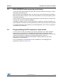
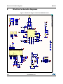
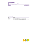
UM1678
User manual
Evaluation kit for RX95HF NFC transceiver
Introduction
The EVAL-RX95HF is an evaluation kit for RX95HF NFC transceiver. This component is a
13.56 MHz near field communication transceiver for NFC tag emulation. It can be used with
any NFC reader/writer (NFC smartphone, DEMO-CR95HF-A board) to exchange NDEF
messages (URI, VCARD, URL) or proprietary data. The firmware embeds two kinds of
applications:
•
NFC Type 4 tag emulation
•
IAP (In Application Programming) through the RF Field
The communication protocol is based on the NFC Forum digital protocol (part A) and Type 4.
The EVAL-RX95HF is powered through the USB bus. It includes an RX95HF transceiver for
tag emulation, a 47 x 34 mm 13.56 MHz inductive etched antenna and its associated tuning
components. The RX95HF communicates with the STM32F103RF 32-bit MCU via the SPI bus.
• Ready-to-use printed circuit board
– RX95HF-VMD5 13.56 MHz NFC transceiver for tag emulation (VFQFPN32 5x5 package)
– STM32F103RFT6 64LQFP 32-bit microcontroller, with 768 Kbytes of Flash memory
– 47 x 34 mm 13.56 MHz inductive antenna etched on PCB and associated circuitry
– USB miniB connector for board powering
– LED indicating the presence of an RF field
– Microcontroller reset button
– Joystick for menu selection
– JTAG connector for microcontroller firmware upgrade and debug
– LCD screen (MB895 board)
•
USB cable: Type A / mini B
•
Associated firmware and Android application
–
On-board firmware for the NFC 14443A Tag emulator (NDEF, URL)
–
Android application for "RX95HF Upgrade Firmware" smartphone
Figure 1. EVAL-RX95HF RF transceiver board with LCD screen plugged
October 2013
DocID025352 Rev 1
1/10
www.st.com
Contents
UM1678
Contents
1
Quick start . . . . . . . . . . . . . . . . . . . . . . . . . . . . . . . . . . . . . . . . . . . . . . . . . 4
2
Features . . . . . . . . . . . . . . . . . . . . . . . . . . . . . . . . . . . . . . . . . . . . . . . . . . . 5
3
Hardware and layout description . . . . . . . . . . . . . . . . . . . . . . . . . . . . . . . 6
3.1
EVAL-RX95HF board description . . . . . . . . . . . . . . . . . . . . . . . . . . . . . . . . 6
3.2
EVAL-RX95HF board powering and startup . . . . . . . . . . . . . . . . . . . . . . . . 7
3.3
Program/debug the RF transceiver demo board . . . . . . . . . . . . . . . . . . . . 7
4
Electrical schematic diagrams . . . . . . . . . . . . . . . . . . . . . . . . . . . . . . . . . 8
5
Revision history . . . . . . . . . . . . . . . . . . . . . . . . . . . . . . . . . . . . . . . . . . . . 9
2/10
DocID025352 Rev 1
UM1678
List of figures
List of figures
Figure 1.
Figure 2.
Figure 3.
Figure 4.
EVAL-RX95HF RF transceiver board with LCD screen plugged . . . . . . . . . . . . . . . . . . . . . 1
Functional block diagram . . . . . . . . . . . . . . . . . . . . . . . . . . . . . . . . . . . . . . . . . . . . . . . . . . . 6
EVAL-RX95HF RF transceiver board with callouts. . . . . . . . . . . . . . . . . . . . . . . . . . . . . . . . 6
Schematic diagram of the EVAL-RX95HF board . . . . . . . . . . . . . . . . . . . . . . . . . . . . . . . . . 8
DocID025352 Rev 1
3/10
3
Quick start
1
UM1678
Quick start
The EVAL-RX95HF kit is a ready-to-use development kit used to evaluate some functions
and performances of the RF transceiver RX95HF for NFC Tag emulation. The RF
communication supports ISO/IEC 14443 Type A communication in NFC Tag Emulation
mode.
The ST Android application "RX95HF Upgrade Firmware" shows a proprietary IAP
application. The user can upload from the NFC reader (NFC Phone or RFID reader) the
firmware of the STM32F103 of the EVAL-RX95HF board and boot on it.
For more information on the RX95HF evaluation kit and associated demonstration software,
please visit www.st.com/nfc-rfid.
4/10
DocID025352 Rev 1
UM1678
2
Features
Features
•
RX95HF, a 13.56-MHz multi-protocol contactless transceiver IC with SPI serial access
communication
•
2-turn, 13.56-MHz etched loop antenna (47 mm x 34 mm) with associated tuning circuit
•
STM32F103RFT6, a 32-bit microcontroller with 728 Kbytes of Flash memory and USB
interface in a 64-pin LQFP package
•
KF33BDT, a 3.3 V low dropout (LDO) voltage regulator
•
USB mini B connector
•
NX2016SA, a 27.12-MHz EXS00A-CS01188 crystal oscillator for RX95HF transceiver
•
HC-49SD 8.000MHz 20pF/80ppm for STM32
•
20-pin JTAG connector for STM32 programming and debugging
•
1 push-button (Reset)
•
1 joystick (4 directions + select)
DocID025352 Rev 1
5/10
9
Hardware and layout description
UM1678
3
Hardware and layout description
3.1
EVAL-RX95HF board description
Figure 2. Functional block diagram
Loop
antenna
Antenna
tuning
circuit
SPI
bus
RX95HF
LCD screen
USB
connector
STM32F103R
JTAG
connector
MS32393V1
Figure 3. EVAL-RX95HF RF transceiver board with callouts
20-pin JTAG
connector
STM32F1
Ground probe
RF field
detection LED
RF matching
components
LCD board
connectors
LCD regulator
USB connector
power supply
Joystick
Reset button
USB connect/disconnect jumper
(must be on 1-2 position)
RX95HF RF IC
2-turn, 13.56 MHz
loop antenna
MS32399V1
6/10
DocID025352 Rev 1
UM1678
3.2
Hardware and layout description
EVAL-RX95HF board powering and startup
The RF transceiver demonstration board is powered by the USB bus via a Type A / mini B
USB cable connected to a PC.
When powered up, the RX95HF starts in an autonomous mode called "NFC tag emulation".
When an NFC reader is present in front of the board antenna, the red LED1 lights up when
an RF field is detected.
The NFC reader, in tag hunting mode (native application of Android phone), will get the ST
web site URL: www.st.com from the RX95HF.
If "RX95HF Upgrade Firmware" Android application is installed on an NFC smartphone, an
EVAL-RX95HF new firmware can be uploaded and the MCU reboots with this new firmware.
A complete description of the firmware and Android application can be found in application
notes posted on ST web site.
3.3
Program/debug the RF transceiver demo board
In order to flash or debug an STM32 microcontroller application on the EVAL-RX95HF
board, simply connect the 20-pin JTAG/SWD flat ribbon of the STLINK/V2 in-circuit
debugger and programmer to the RF transceiver demonstration board JTAG connector (J3).
Launch STLink Utility PC software (can be downloaded from ST web site:
http://www.st.com/web/en/catalog/tools/PF258168. STM32F103RFT6 is part of the
STM32F10x XL-density family.
For more information or documentation on the STLINK/V2 in-circuit debugger and
programmer, please visit www.st.com.
DocID025352 Rev 1
7/10
9
R26
1M
6
6
SW1
4,7nF
C26
1
2
3
4
5
3.3V
R11
10k
20pF
C4
20pF
Mini USB
VDD
DD+
OTG
GND
J2
C7
100nF
6
6
C1
/RESET
R4
1M
L7
4
ST2
744232090
R36
10k
R41
10k
R42
10k
R39
10k
R40
10k
JTDO
/RESET
/JTRST
JTDI
JTMS
JTCK
R35
10k
R34
10k
1
3
5
7
9
11
13
15
17
19
J3
Q2
BC817
1
3
5
7
9
11
13
15
17
19
R25
47k
3.3V
U5V
R33
10k
3.3V
3
2
3.3V
2
4
6
8
10
12
14
16
18
20
100nF
100nF
2
4
6
8
10
12
14
16
18
20
R27
36k
R22
10k
U5V
C19
10uF
C15
C14
VDD1
10k
+
C20
USB_DM
USB_DP
JTMS
JTCK
JTDI
R7
41
42
43
44
45
46
49
50
1.5k
R28
Q1
BC817
R21 10
PC0
PC1
PC2
PC3
PC4
PC5
PC6
PC7
PB8
PB9
PB10
PB11
PB12
PB13
PB14
PB15
PB0
PB1
PB2/BOOT1
PB3/JTDO
PB4/JNTRST
PB5
PB6
PB7
VSSA
VSS_1
VSS_2
VSS_3
VSS_4
PC8
PC9
PC10
PC11
PC12
PC13-TAMPER-RTC
PC14-OSC32_IN
PC15-OSC32_OUT
USB_DM
USB_DP
STM32F103RFT6
VDDA
VDD_1
VDD_2
VDD_3
VDD_4
VBAT
NRST
BOOT0
OSC_IN/PD0
OSC_OUT/PD1
PD2
PA8
PA9
PA10
PA11
PA12
PA13/JTMS/SWDIO
PA14/JTCK/SWCLK
PA15/JTDI
PA0-WKUP
PA1
PA2
PA3
PA4
PA5
PA6
PA7
U2
R20 10
3.3V
100nF
13
32
48
64
19
1
7
60
5
6
54
14
15
16
17
20
21
22
23
BLM18AG601SN1D
L4
100nF
100nF
3.3V
C13
C12
3.3V
742792641
1 FL1
USB_Disconnect
VDD
C10
100nF
L1
742792042
3.3V
Y1
8MHz
1
2
3
1
2
3
MIRE2
MIRE
MIRE
LCD_RS
/LCD_WR
LCD_CLK
LCD_DO
LCD_DI
JOY_RIGHT
JOY_UP
1k
R2
USB_Disconnect
Interface_Pin
R1
/LCD_CS
JTDO
4.7k
/JTRST
JOY_LEFT
JOY_SEL
JOY_DOWN
MIRE1
12
31
47
63
18
39
40
51
52
53
2
3
4
8
9
10
11
24
25
37
38
61
62
29
30
33
34
35
36
26
27
28
55
56
57
58
59
MIRE
MIRE3
/IRQ_OUT
/IRQ_IN
LCD MIRE
MIRE4
R30
NC
R32
0
R29
NC
R31
0
3.3V
R23
3.3k
R24
3.3k
R17
3.3k
21
10pF
C27
14
12
16
17
18
15
R19
3.3k
3.3V
SPI_MISO
SPI_MOSI
SPI_CLK
/SPI_CS_NFC
R16
NC
R13
0
19
20
R18
3.3k
R15
0
R12
NC
3.3V
Interface_Pin
LED-1206
LED1
3.3V
U5V
1
2
ST1
3.3V
3.3V
1
Vin
U3
KF33BDT
27.12MHz
GND GND
XIN XOUT
Y2
C29
100nF
2
1
/IRQ_OUT
/IRQ_IN
SPI_MISO
SPI_MOSI
SPI_CLK
SPI_SS
SSI_0
SSI_1
ST_R1
1
2
LCD_DO
/RESET
/LCD_CS
LCD_CLK
LCD_DI
LCD_RS
/LCD_WR
XIN
29
9
1
2
3
4
5
6
7
8
1
2
3
4
5
6
7
8
4
3
ST_R0
XOUT
30
GND
DocID025352 Rev 1
3
Vout
C21
1nF
C28
2
10pF
C16
10nF
+
C30
2,2uF
NC
NC
NC
NC
NC
NC
NC
NC
NC
NC
NC
ST_R4
RX2
RX1
ST_R3
U1
RX95HF
C31
100nF
C11
1uF
C9
100nF
L2
742792042
3.3V
LCD Connector
VDD
VCI
GND
GND
BL_VDD
BL_Control
BL_GND
BL_GND
J1-2
LCD Connector
/CS
SCL
SDI
RS
/WR
/RD
SDO
/RESET
J1-1
BACK PLANE
33
+
13
32
31
VPS
ST_R5
GND_TX
8/10
GND_RX
GND
3
NC
2
744232222
NC
C24
C23
NC
10k
10k
R6
R8
R9
C25
NC
C22
NC
0
Date: 14/10/2013
Reference: MB1132
EVAL-RX95HF
R38
0
R37
742792042
0
RRX2
0
RRX1
R10 10k
10k
10k
R5
L9
742792042
L8
NC
C18
Size: C
Title:
C17
NC
+
NC
4
L6
L5
1 FL2
3
4
7
10
11
23
24
25
26
27
28
2
6
5
1
NC
R14
L3
NC
3.3V
3.3V
3.3V
56pF
Sheet: 1
of 1
Revision: B-02
220pF
Cb
JOY_SEL
JOY_RIGHT
JOY_DOWN
JOY_LEFT
JOY_UP
MT008-A
DOWN
LEFT
RIGHT
UP
Selection
COMMON
U4
Ca
3
1
4
6
JOY_DOWN
JOY_LEFT
JOY_RIGHT
JOY_UP
5
2
10
R3
JOY_SEL
Rq
4.7k
1
2
ANTENNA
ANTENNA
ant1
STMicroelectronics
MMY Division
190, avenue Célestin COQ
13106 ROUSSET Cedex
FRANCE
C2
100nF
C3
100nF
C5
100nF
C6
100nF
C8
100nF
4
8
22
/IRQ_IN
/IRQ_OUT
/SPI_CS_NFC
SPI_CLK
SPI_MISO
SPI_MOSI
Electrical schematic diagrams
UM1678
Electrical schematic diagrams
Figure 4. Schematic diagram of the EVAL-RX95HF board
UM1678
5
Revision history
Revision history
Table 1. Document revision history
Date
Revision
31-Oct-2013
1
Changes
Initial release.
DocID025352 Rev 1
9/10
9
UM1678
Please Read Carefully:
Information in this document is provided solely in connection with ST products. STMicroelectronics NV and its subsidiaries (“ST”) reserve the
right to make changes, corrections, modifications or improvements, to this document, and the products and services described herein at any
time, without notice.
All ST products are sold pursuant to ST’s terms and conditions of sale.
Purchasers are solely responsible for the choice, selection and use of the ST products and services described herein, and ST assumes no
liability whatsoever relating to the choice, selection or use of the ST products and services described herein.
No license, express or implied, by estoppel or otherwise, to any intellectual property rights is granted under this document. If any part of this
document refers to any third party products or services it shall not be deemed a license grant by ST for the use of such third party products
or services, or any intellectual property contained therein or considered as a warranty covering the use in any manner whatsoever of such
third party products or services or any intellectual property contained therein.
UNLESS OTHERWISE SET FORTH IN ST’S TERMS AND CONDITIONS OF SALE ST DISCLAIMS ANY EXPRESS OR IMPLIED
WARRANTY WITH RESPECT TO THE USE AND/OR SALE OF ST PRODUCTS INCLUDING WITHOUT LIMITATION IMPLIED
WARRANTIES OF MERCHANTABILITY, FITNESS FOR A PARTICULAR PURPOSE (AND THEIR EQUIVALENTS UNDER THE LAWS
OF ANY JURISDICTION), OR INFRINGEMENT OF ANY PATENT, COPYRIGHT OR OTHER INTELLECTUAL PROPERTY RIGHT.
ST PRODUCTS ARE NOT DESIGNED OR AUTHORIZED FOR USE IN: (A) SAFETY CRITICAL APPLICATIONS SUCH AS LIFE
SUPPORTING, ACTIVE IMPLANTED DEVICES OR SYSTEMS WITH PRODUCT FUNCTIONAL SAFETY REQUIREMENTS; (B)
AERONAUTIC APPLICATIONS; (C) AUTOMOTIVE APPLICATIONS OR ENVIRONMENTS, AND/OR (D) AEROSPACE APPLICATIONS
OR ENVIRONMENTS. WHERE ST PRODUCTS ARE NOT DESIGNED FOR SUCH USE, THE PURCHASER SHALL USE PRODUCTS AT
PURCHASER’S SOLE RISK, EVEN IF ST HAS BEEN INFORMED IN WRITING OF SUCH USAGE, UNLESS A PRODUCT IS
EXPRESSLY DESIGNATED BY ST AS BEING INTENDED FOR “AUTOMOTIVE, AUTOMOTIVE SAFETY OR MEDICAL” INDUSTRY
DOMAINS ACCORDING TO ST PRODUCT DESIGN SPECIFICATIONS. PRODUCTS FORMALLY ESCC, QML OR JAN QUALIFIED ARE
DEEMED SUITABLE FOR USE IN AEROSPACE BY THE CORRESPONDING GOVERNMENTAL AGENCY.
Resale of ST products with provisions different from the statements and/or technical features set forth in this document shall immediately void
any warranty granted by ST for the ST product or service described herein and shall not create or extend in any manner whatsoever, any
liability of ST.
ST and the ST logo are trademarks or registered trademarks of ST in various countries.
Information in this document supersedes and replaces all information previously supplied.
The ST logo is a registered trademark of STMicroelectronics. All other names are the property of their respective owners.
© 2013 STMicroelectronics - All rights reserved
STMicroelectronics group of companies
Australia - Belgium - Brazil - Canada - China - Czech Republic - Finland - France - Germany - Hong Kong - India - Israel - Italy - Japan Malaysia - Malta - Morocco - Philippines - Singapore - Spain - Sweden - Switzerland - United Kingdom - United States of America
www.st.com
10/10
DocID025352 Rev 1