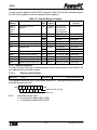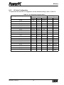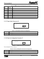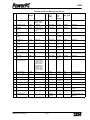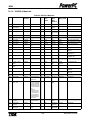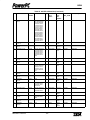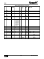
1
PowerPC 603/604 Reference Design Technical Specification Release 2.1 This document provides a detailed technical description of the PowerPC 603/604 Reference Design. It is intended as a first source of information for both hardware and software designers. Where appropriate, other documents are referenced. Document Number: MPRH01TSU-02 August, 9 1995 R International Business Machines Corporation, 1995. Printed in the United States of America 8/95. All Rights reserved. IBM Microelectronics, PowerPC, PowerPC 601, PowerPC 603, PowerPC 603e, PowerPC 604, RISCWatch, and AIX are trademarks of the IBM corporation. IBM and the IBM logo are registered trademarks of the IBM corporation. Other company names and product identifiers are trademarks of the respective companies. This document contains information which is subject to change by IBM without notice. IBM assumes no responsibility or liability for any use of the information contained herein. Nothing in this document shall operate as an express or implied license or indemnity under the intellectual property rights of IBM or third parties. The products described in this document are not intended for use in implantation or other direct life-support applications where malfunction may result in physical harm or injury to persons. NO WARRANTIES OF ANY KIND, INCLUDING BUT NOT LIMITED TO, THE IMPLIED WARRANTIES OF MERCHANTABILITY OR FITNESS FOR A PARTICULAR PURPOSE, ARE OFFERED IN THIS DOCUMENT. Contacts USA and Canada: IBM Microelectronics Division 1580 Route 52, Bldg. 504 Hopewell Junction, NY 12533-6531 Tel: (800) PowerPC Fax: (800) PowerFax Japan: IBM 800, Ichimiyake Yasu–cho, Yasu–gun Shiga–ken, Japan 520–23 Tel: (81) 775–87–4745 Fax: (81) 775–87–4735 Europe: IBM La Pompignane BP 1021 34006 Montpellier, France Tel: (33) 6713–5757 (Français) (33) 6713–5756 (Italiano) Fax: (33) 6713–5750 ( from Paris add 16) Europe: IBM Informations Systeme GmbH Laatzener Str. 1 30539 Hannover, Germany Tel: (49) 511–516–3444 (English) (49) 511–516–3555 (Deutsche) Fax: (49) 511–516–3888 ESD Warning The motherboard and memory cards contain CMOS devices which are very susceptible to ElectroStatic Discharge (ESD). DO NOT remove them from the antistatic bags until you have connected yourself to an acceptable ESD grounding strap. Work in a static free environment and be sure any person or equipment coming into contact with the cards do not have a static charge. The cards are particularly susceptible until they are placed in a properly designed enclosure. Bench work should be done by persons connected to ESD grounding straps. 2 MPRH08TSU-02 IBM POWERPCTM 603/604 REFERENCE DESIGN AGREEMENT BEFORE READING THE REST OF THE DOCUMENT, YOU SHOULD CAREFULLY READ THE FOLLOWING TERMS AND CONDITIONS. OPENING THE PACKAGE INDICATES YOUR ACCEPTANCE OF THESE TERMS AND CONDITIONS. IF YOU DO NOT AGREE WITH THEM, YOU SHOULD PROMPTLY RETURN THE PACKAGE UNOPENED TO YOUR IBM SALES OFFICE. International Business Machines Corporation (”IBM”) agrees to provide you a PowerPC 603/604 Reference Design (Reference Design) in return for your promise to use reasonable efforts to develop a system based on the technology in the Reference Design. The Reference Design contains documentation and software listed below: Documentation PowerPC 603e RISC Microprocessor Hardware Specification PowerPC 603e RISC Microprocessor Technical Summary PowerPC 603/604 RISC Microprocessor Hardware Specification PowerPC 603/604 Reference Design Technical Specification IBM PowerPC 603/604 Reference Board Design Files (on 8mm tape) IBM PowerPC 604 Reference Board Mfg. Data Files (in Gerber format) IBM14N1372 Data Sheet IBM11D4360B Data Sheet Motorola MPC970 Data Sheet Altera 5130 Data Sheet Integrated Device Technology IDT71216 Data Sheet LICENSE TO SOFTWARE The software is licensed not sold. IBM, or the applicable IBM country organization, grants you a license for the software only in the country where you received the software. Title to the physical software and documentation (not the information contained in such documentation) transfers to you upon your acceptance of these terms and conditions. The term ”software” means the original and all whole or partial copies of it, including modified copies or portions merged into other programs. IBM retains title to the software. IBM owns, or has licensed from the owner, copyrights to the software provided under this agreement. The terms of this Agreement apply to all of the hardware, software and documentation provided to you as part of the Reference Design. With regard to the software provided hereunder, it is understood and agreed that you intend to use the software solely for the purpose of designing PowerPC compatible products, testing your designs, and making your own independent determination of whether you wish to eventually manufacture PowerPC compatible products commercially. In accordance with this understanding, IBM hereby grants you the rights to: a) use, run, and copy the software, but only make such number of copies and run on such number of machines as are reasonably necessary for the purpose of designing PowerPC compatible products and testing such designs; and b) copy the software for the purpose of making one archival or backup copy. With regard to any copy made in accordance with the foregoing license, you must reproduce any copyright notice appearing thereon. With regard to the software provided hereunder, you may not: a) use, copy, modify or merge the software, except as provided in this license; b) reverse assemble or reverse compile it; or c) sell, sublicense, rent. lease, assign or otherwise transfer it. In the event that you no longer wish to use the software, you will return it to IBM. LICENSE TO DESIGN DOCUMENTATION With regard to the design documentation provided hereunder, it is understood that you intend to use such documentation solely for the purpose of designing your own PowerPC compatible products, testing your designs, and making your own independent determination of whether you wish to eventually manufacture PowerPC compatible products commercially. In accordance with this understanding, IBM hereby grants you the right to: a) use the design documentation for the purpose of designing PowerPC compatible products and testing such designs; b) make derivative works of the design documentation for the purpose of designing PowerPC compatible products, and testing such designs; and c) make copies of the design documentation and any such derivative works, but only such numbers as are reasonably necessary for designing PowerPC compatible products and testing such designs. With regard to any copy made in accordance with the forgoing license, you must reproduce any copyright notice appearing thereon. With regard to the design documentation provided hereunder, you may not: a) use, copy, modify, or merge the design documentation as provided in this license; or b) sell, sublicense, rent, lease, assign, or otherwise transfer it. In the event you no longer wish to use the design documentation or any derivative versions thereof, you must return them to IBM. DISCLAIMER OF WARRANTY IBM does not represent or warrant that the Reference Design (which may contain prototype items): a) meets any particular requirements; b) operates uninterrupted; c) is error free; or d) is non–infringing of any patent, copyright, or other intellectual property right of any third party. IBM makes no representation or warranty regarding the performance or compatibility that may be obtained from the use of the Reference Design or that the Reference Design is adequate for any use. The Reference Design may contain errors and may not provide the level of completeness, functionality, support, performance, reliability, or ease of use available with other products, whether or not similar to the Reference Design. IBM does not represent or warrant that errors or other defects will be identified or corrected. THE REFERENCE DESIGN IS PROVIDED ”AS IS” WITH ALL FAULTS, WITHOUT WARRANTY OF ANY KIND, EXPRESS OR IMPLIED, INCLUDING, BUT NOT LIMITED TO, THE IMPLIED WARRANTIES OF MERCHANTABILITY AND FITNESS FOR A PARTICULAR PURPOSE. THE ENTIRE RISK AS TO THE QUALITY AND PERFORMANCE OF THE REFERENCE DESIGN IS WITH YOU. Some jurisdictions do not allow exclusion of implied warranties, so the above exclusions may not apply to you. MPRH08TSU-02 3 LIMITATION OF REMEDIES IBM’s entire cumulative liability and your exclusive remedy for damages for all causes, claims or actions wherever and whenever asserted relating in any way to the subject matter of this agreement including the contents of the Reference Design and any components thereof, is limited to twenty five thousand dollars ($25,000.00) or its equivalent in your local currency and is without regard to the number of items in the Reference Design that caused the damage. This limitation will apply, except as otherwise stated in this Section, regardless of the form of the action, including negligence. This limitation will not apply to claims by you for bodily injury or damages to real property or tangible personal property. In no event will IBM be liable for any lost profits, lost savings, or any incidental damages or economic consequential damages, even if IBM has been advised of the possibility of such damages, or for any damages caused by your failure to perform your responsibilities. In addition, IBM will not be liable for any damages claimed by you based on any third party claim. Some jurisdictions do not allow these limitations or exclusions, so they may not apply to you. RISK OF LOSS You are responsible for all risk of loss or damage to the Reference Design upon its delivery to you. IBM TRADEMARKS AND TRADE NAMES This Agreement does not give you any rights to use any of IBM’s trade names or trademarks. You agree that should IBM determine that any of your advertising, promotional, or other materials are inaccurate or misleading with respect to IBM trademarks or trade names, that you will, upon written notice from IBM, change or correct such materials at your expense. NO IMPLIED LICENSE TO IBM INTELLECTUAL PROPERTY Notwithstanding the fact that IBM is hereby providing design information for your convenience, you expressly understand and agree that, except for the rights granted under sections 1 and 2 above, no right or license of any type is granted, expressly or impliedly, under any patents, copyrights, trade secrets, trademarks, or other intellectual property rights of IBM. Moreover, you understand and agree that in the event you wish to be granted any license beyond the scope of the expressly stated herein, you will contact IBM’s Intellectual Property Licensing and Services Office (currently located at 500 Columbus Avenue, Thornwood, N.Y.), or such other IBM offices responsible for the licensing of IBM intellectual property, when you seek the license. YOUR ASSUMPTION OF RISK You shall be solely responsible for your success in designing, developing, manufacturing, distributing, and marketing any product(s), or portion(s), where use of all or any part of the Reference Design is involved. You are solely responsible for any claims, warranties, representations, indemnities and liabilities you undertake with your customers, distributors, resellers or others, concerning any product(s) or portion(s) of product(s) where use of all or any part of the Reference Design is involved. You assume the risk that IBM may introduce other Reference Design that are somehow better than the Reference Design which is the subject of this Agreement. Furthermore, you accept sole responsibility for your decision to select and use the Reference Design; for attainment or non-attainment of any schedule, performance, cost, reliability, maintainability, quality, manufacturability or the like, requirements, or goals, self–imposed by you or accepted by you from others, concerning any product(s) or portion(s) of product(s), or for any delays, costs, penalties, charges, damages, expenses, claims or the like, resulting from such non-attainment, where use of all or any part of the Reference Design is involved. GENERAL In the event there is a conflict between the terms of this Agreement and the terms printed or stamped on any item or any ambiguities with respect thereto, including documentation, contained in the Reference Design, the terms of this Agreement control to the extent IBM is afforded greater protection thereby. IBM may terminate this Agreement if you fail to comply with the terms and conditions of this Agreement. Upon termination of this Agreement, you must destroy all copies of the software and documentation. You are responsible for payment of any taxes, including personal property taxes, resulting from this Agreement. Neither party may bring an action hereunder, regardless of form, more than one (1) year after the cause of the action arose. If you acquired the Reference Design in the United States, this Agreement is governed by the laws of the State of New York. In the event of litigations, trial shall be in New York without a jury. If you acquired the Reference Design in Canada, this Agreement is governed by the laws of the Province of Ontario; otherwise, this Agreement is governed by the laws of the country in which you acquired the Reference Design. All obligations and duties which, by their nature, survive termination or expiration of this Agreement, shall remain in effect beyond termination or expiration of this Agreement, and shall bind IBM, you and your successors and assigns. If any section or paragraph of this Agreement is found by competent authority to be invalid, illegal or unenforceable in any respect for any reason, the validity, legality, and enforceability of any such section or paragraph in every other respect, and the remainder of this Agreement, shall continue in effect so long as it still expresses the intent of the parties. If the intent of the parties cannot be preserved, the parties will attempt to renegotiate this Agreement and failing renegotiation, this Agreement will then be terminated. The headings in this Agreement shall not affect the meaning or interpretation of this Agreement in any way. No failure by IBM in exercising any right, power or remedy under this Agreement shall serve as a waiver of any such right, power or remedy. Neither this Agreement nor any activities hereunder will impair any right of IBM to develop, manufacture, use or market, directly or indirectly, alone or with others, any products or services competitive with those offered or to be offered by you; nor will this Agreement or any activities hereunder require IBM to disclose any business planning information to you. You agree to comply with all applicable government laws and regulations. Any changes to this Agreement must be in writing and signed by the parties. 4 MPRH08TSU-02 Table of Contents Section 1 Introduction . . . . . . . . . . . . . . . . . . . . . . . . . . . . . . . . . . . . . . . . . . . . . . . . . 1.1 IBM Reference Products . . . . . . . . . . . . . . . . . . . . . . . . . . . . . . . . . . . . . . . . 1.1.1 Reference Design . . . . . . . . . . . . . . . . . . . . . . . . . . . . . . . . . . . . . . . . . . . 1.1.2 Reference Board . . . . . . . . . . . . . . . . . . . . . . . . . . . . . . . . . . . . . . . . . . . . 1.1.3 Reference Firmware . . . . . . . . . . . . . . . . . . . . . . . . . . . . . . . . . . . . . . . . . 1.1.4 Reference System . . . . . . . . . . . . . . . . . . . . . . . . . . . . . . . . . . . . . . . . . . . 1.2 Purpose . . . . . . . . . . . . . . . . . . . . . . . . . . . . . . . . . . . . . . . . . . . . . . . . . . . . . . 1.3 Reference Design Overview . . . . . . . . . . . . . . . . . . . . . . . . . . . . . . . . . . . . . 1.3.1 The CPU . . . . . . . . . . . . . . . . . . . . . . . . . . . . . . . . . . . . . . . . . . . . . . . . . . . 1.3.2 IBM27-82660 Bridge . . . . . . . . . . . . . . . . . . . . . . . . . . . . . . . . . . . . . . . . . 1.3.3 L2 Cache . . . . . . . . . . . . . . . . . . . . . . . . . . . . . . . . . . . . . . . . . . . . . . . . . . . 1.3.4 System Memory . . . . . . . . . . . . . . . . . . . . . . . . . . . . . . . . . . . . . . . . . . . . . 1.3.5 PCI Bus . . . . . . . . . . . . . . . . . . . . . . . . . . . . . . . . . . . . . . . . . . . . . . . . . . . . 1.3.6 Flash ROM . . . . . . . . . . . . . . . . . . . . . . . . . . . . . . . . . . . . . . . . . . . . . . . . . 1.3.7 ISA Bus . . . . . . . . . . . . . . . . . . . . . . . . . . . . . . . . . . . . . . . . . . . . . . . . . . . . 1.3.8 Time of Day Clock . . . . . . . . . . . . . . . . . . . . . . . . . . . . . . . . . . . . . . . . . . . 1.3.9 PS/2t Compatible Keyboard/Mouse Controller . . . . . . . . . . . . . . . . . 1.3.10 System Clocks . . . . . . . . . . . . . . . . . . . . . . . . . . . . . . . . . . . . . . . . . . . . . . 1.3.11 System I/O EPLD . . . . . . . . . . . . . . . . . . . . . . . . . . . . . . . . . . . . . . . . . . . . 1.4 Quickstart Peripheral List . . . . . . . . . . . . . . . . . . . . . . . . . . . . . . . . . . . . . . . 1.5 Reference Design Level . . . . . . . . . . . . . . . . . . . . . . . . . . . . . . . . . . . . . . . . 17 17 17 17 17 18 18 19 19 19 19 20 21 21 21 21 21 21 21 22 22 Section 2 CPU and CPU Bus . . . . . . . . . . . . . . . . . . . . . . . . . . . . . . . . . . . . . . . . . . . 2.1 CPU Bus Masters . . . . . . . . . . . . . . . . . . . . . . . . . . . . . . . . . . . . . . . . . . . . . . 2.1.1 603e CPU . . . . . . . . . . . . . . . . . . . . . . . . . . . . . . . . . . . . . . . . . . . . . . . . . . 2.1.2 604 CPU . . . . . . . . . . . . . . . . . . . . . . . . . . . . . . . . . . . . . . . . . . . . . . . . . . . 2.2 System Response by CPU Bus Transfer Type . . . . . . . . . . . . . . . . . . . . . 2.3 System Response by CPU Bus Address Range . . . . . . . . . . . . . . . . . . . . 2.3.1 Address Mapping for Non-Contiguous I/O . . . . . . . . . . . . . . . . . . . . . . 2.3.2 Address Mapping for Contiguous I/O . . . . . . . . . . . . . . . . . . . . . . . . . . . 2.3.3 PCI Final Address Formation . . . . . . . . . . . . . . . . . . . . . . . . . . . . . . . . . 2.4 CPU to Memory Transfers . . . . . . . . . . . . . . . . . . . . . . . . . . . . . . . . . . . . . . 2.4.1 LE Mode . . . . . . . . . . . . . . . . . . . . . . . . . . . . . . . . . . . . . . . . . . . . . . . . . . . 2.5 CPU to PCI Transactions . . . . . . . . . . . . . . . . . . . . . . . . . . . . . . . . . . . . . . . 2.5.1 CPU to PCI Read . . . . . . . . . . . . . . . . . . . . . . . . . . . . . . . . . . . . . . . . . . . . 2.5.2 CPU to PCI Write . . . . . . . . . . . . . . . . . . . . . . . . . . . . . . . . . . . . . . . . . . . . 2.5.2.1 Eight-Byte Writes to the PCI (Memory and I/O) . . . . . . . . . . . . . . . . . 2.5.3 CPU to PCI Memory Transactions . . . . . . . . . . . . . . . . . . . . . . . . . . . . . 2.5.4 CPU to PCI I/O Transactions . . . . . . . . . . . . . . . . . . . . . . . . . . . . . . . . . . 2.5.5 CPU to PCI Configuration Transactions . . . . . . . . . . . . . . . . . . . . . . . . 2.5.5.1 Preferred Method of Generating PCI Configuration Transactions . 25 25 25 26 26 28 28 30 30 30 31 31 31 31 31 32 32 32 32 MPRH08TSU-02 5 2.5.5.2 650 Bridge compatible method . . . . . . . . . . . . . . . . . . . . . . . . . . . . . . . 2.5.6 CPU to PCI Interrupt Acknowledge Transaction . . . . . . . . . . . . . . . . . 2.5.7 PCI Lock . . . . . . . . . . . . . . . . . . . . . . . . . . . . . . . . . . . . . . . . . . . . . . . . . . . 2.6 CPU to ROM Transfers . . . . . . . . . . . . . . . . . . . . . . . . . . . . . . . . . . . . . . . . . 2.6.1 CPU to ROM Read . . . . . . . . . . . . . . . . . . . . . . . . . . . . . . . . . . . . . . . . . . 2.6.2 CPU to ROM Write . . . . . . . . . . . . . . . . . . . . . . . . . . . . . . . . . . . . . . . . . . 2.6.2.1 ROM Write Protection . . . . . . . . . . . . . . . . . . . . . . . . . . . . . . . . . . . . . . . 2.6.3 CPU to BCR Transfers . . . . . . . . . . . . . . . . . . . . . . . . . . . . . . . . . . . . . . . 32 33 33 33 34 34 34 34 Section 3 PCI Bus . . . . . . . . . . . . . . . . . . . . . . . . . . . . . . . . . . . . . . . . . . . . . . . . . . . . . 3.1 PCI Transaction Decoding . . . . . . . . . . . . . . . . . . . . . . . . . . . . . . . . . . . . . . 3.1.1 PCI Transaction Decoding By Bus Command . . . . . . . . . . . . . . . . . . . 3.1.2 PCI Memory Transaction Decoding By Address Range . . . . . . . . . . . 3.1.3 PCI I/O Transaction Decoding . . . . . . . . . . . . . . . . . . . . . . . . . . . . . . . . . 3.1.4 ISA Master Considerations . . . . . . . . . . . . . . . . . . . . . . . . . . . . . . . . . . . 3.2 PCI Transaction Details . . . . . . . . . . . . . . . . . . . . . . . . . . . . . . . . . . . . . . . . . 3.2.1 Bus Snooping on PCI to Memory Cycles . . . . . . . . . . . . . . . . . . . . . . . 3.2.2 PCI to PCI Peer Transactions . . . . . . . . . . . . . . . . . . . . . . . . . . . . . . . . . 3.2.3 PCI to System Memory Transactions . . . . . . . . . . . . . . . . . . . . . . . . . . . 3.3 Bus Arbitration Logic . . . . . . . . . . . . . . . . . . . . . . . . . . . . . . . . . . . . . . . . . . . 3.4 Other PCI Considerations . . . . . . . . . . . . . . . . . . . . . . . . . . . . . . . . . . . . . . . 35 35 36 36 38 38 38 39 39 39 41 41 Section 4 ISA Bus . . . . . . . . . . . . . . . . . . . . . . . . . . . . . . . . . . . . . . . . . . . . . . . . . . . . . 4.1 The ISA Bridge . . . . . . . . . . . . . . . . . . . . . . . . . . . . . . . . . . . . . . . . . . . . . . . . 4.2 Address Ranges . . . . . . . . . . . . . . . . . . . . . . . . . . . . . . . . . . . . . . . . . . . . . . . 4.3 ISA Bus Concurrency . . . . . . . . . . . . . . . . . . . . . . . . . . . . . . . . . . . . . . . . . . 4.4 ISA Bus Masters and IGN_PCI_AD31 . . . . . . . . . . . . . . . . . . . . . . . . . . . . 4.5 DMA . . . . . . . . . . . . . . . . . . . . . . . . . . . . . . . . . . . . . . . . . . . . . . . . . . . . . . . . . 4.5.1 Supported DMA Paths . . . . . . . . . . . . . . . . . . . . . . . . . . . . . . . . . . . . . . . 4.5.2 DMA Timing . . . . . . . . . . . . . . . . . . . . . . . . . . . . . . . . . . . . . . . . . . . . . . . . 4.5.3 Scatter-Gather . . . . . . . . . . . . . . . . . . . . . . . . . . . . . . . . . . . . . . . . . . . . . . 4.6 X-Bus . . . . . . . . . . . . . . . . . . . . . . . . . . . . . . . . . . . . . . . . . . . . . . . . . . . . . . . . 4.6.1 Control Signal Decodes . . . . . . . . . . . . . . . . . . . . . . . . . . . . . . . . . . . . . . 4.6.2 Keyboard/Mouse Controller . . . . . . . . . . . . . . . . . . . . . . . . . . . . . . . . . . . 4.6.3 Real Time Clock (RTC) . . . . . . . . . . . . . . . . . . . . . . . . . . . . . . . . . . . . . . . 4.6.4 PCI Adapter Card Presence Detect Register . . . . . . . . . . . . . . . . . . . . 4.6.5 L2 SRAM Identification Register . . . . . . . . . . . . . . . . . . . . . . . . . . . . . . . 4.6.6 Planar ID Detection Register . . . . . . . . . . . . . . . . . . . . . . . . . . . . . . . . . . 4.6.7 DRAM Presence Detection . . . . . . . . . . . . . . . . . . . . . . . . . . . . . . . . . . . 4.6.7.1 DRAM SIMM 1-2 Memory ID Register . . . . . . . . . . . . . . . . . . . . . . . . . 4.6.7.2 DRAM SIMM 3-4 Memory ID Register . . . . . . . . . . . . . . . . . . . . . . . . . 4.7 Miscellaneous . . . . . . . . . . . . . . . . . . . . . . . . . . . . . . . . . . . . . . . . . . . . . . . . . 4.7.1 Speaker Support . . . . . . . . . . . . . . . . . . . . . . . . . . . . . . . . . . . . . . . . . . . . 43 43 44 44 44 46 46 46 46 47 47 47 47 47 46 48 49 49 49 50 60 Section 5 System I/O EPLD . . . . . . . . . . . . . . . . . . . . . . . . . . . . . . . . . . . . . . . . . . . . 5.1 System Register Support . . . . . . . . . . . . . . . . . . . . . . . . . . . . . . . . . . . . . . . 51 51 6 MPRH08TSU-02 5.1.1 External Register Support . . . . . . . . . . . . . . . . . . . . . . . . . . . . . . . . . . . . 5.1.2 Internal Registers . . . . . . . . . . . . . . . . . . . . . . . . . . . . . . . . . . . . . . . . . . . . 5.1.2.1 Storage Light Register . . . . . . . . . . . . . . . . . . . . . . . . . . . . . . . . . . . . . . 5.1.2.2 Power Management Control Register 1 . . . . . . . . . . . . . . . . . . . . . . . 5.1.2.3 Power Management Control Register 2 . . . . . . . . . . . . . . . . . . . . . . . 5.1.2.4 Freeze Clock Register (FCR) Low . . . . . . . . . . . . . . . . . . . . . . . . . . . . 5.1.2.5 Freeze Clock Register (FCR) High . . . . . . . . . . . . . . . . . . . . . . . . . . . . 5.2 Signal Descriptions . . . . . . . . . . . . . . . . . . . . . . . . . . . . . . . . . . . . . . . . . . . . 5.3 EPLD Design Equations . . . . . . . . . . . . . . . . . . . . . . . . . . . . . . . . . . . . . . . . 5.3.1 Fit File . . . . . . . . . . . . . . . . . . . . . . . . . . . . . . . . . . . . . . . . . . . . . . . . . . . . . 5.3.2 TDF File . . . . . . . . . . . . . . . . . . . . . . . . . . . . . . . . . . . . . . . . . . . . . . . . . . . . 51 52 52 52 53 53 53 54 57 57 59 Section 6 Memory Systems . . . . . . . . . . . . . . . . . . . . . . . . . . . . . . . . . . . . . . . . . . . . 6.1 DRAM . . . . . . . . . . . . . . . . . . . . . . . . . . . . . . . . . . . . . . . . . . . . . . . . . . . . . . . . 6.1.1 Refresh . . . . . . . . . . . . . . . . . . . . . . . . . . . . . . . . . . . . . . . . . . . . . . . . . . . . 6.1.2 DRAM Presence Detection . . . . . . . . . . . . . . . . . . . . . . . . . . . . . . . . . . . 6.1.3 Organization . . . . . . . . . . . . . . . . . . . . . . . . . . . . . . . . . . . . . . . . . . . . . . . . 6.2 L2 Cache . . . . . . . . . . . . . . . . . . . . . . . . . . . . . . . . . . . . . . . . . . . . . . . . . . . . . 6.2.1 SRAM . . . . . . . . . . . . . . . . . . . . . . . . . . . . . . . . . . . . . . . . . . . . . . . . . . . . . 6.2.2 TagRAM . . . . . . . . . . . . . . . . . . . . . . . . . . . . . . . . . . . . . . . . . . . . . . . . . . . . 6.2.3 L2 Cache Configuration . . . . . . . . . . . . . . . . . . . . . . . . . . . . . . . . . . . . . . 6.3 ROM . . . . . . . . . . . . . . . . . . . . . . . . . . . . . . . . . . . . . . . . . . . . . . . . . . . . . . . . . 6.4 CPU to ROM Transfers . . . . . . . . . . . . . . . . . . . . . . . . . . . . . . . . . . . . . . . . . 6.4.1 CPU to ROM Read . . . . . . . . . . . . . . . . . . . . . . . . . . . . . . . . . . . . . . . . . . 6.4.2 CPU to ROM Write . . . . . . . . . . . . . . . . . . . . . . . . . . . . . . . . . . . . . . . . . . 6.4.2.1 ROM Write Protection . . . . . . . . . . . . . . . . . . . . . . . . . . . . . . . . . . . . . . . 67 67 67 67 68 69 69 72 73 74 74 74 74 75 Section 7.1 7.2 7.3 7.4 7.5 7.6 7.7 7.8 7.9 7.10 7.11 7.12 7 Endian Mode Considerations . . . . . . . . . . . . . . . . . . . . . . . . . . . . . . . . . What the 603/604 CPU Does . . . . . . . . . . . . . . . . . . . . . . . . . . . . . . . . . . . . What the 660 Bridge Does . . . . . . . . . . . . . . . . . . . . . . . . . . . . . . . . . . . . . . Bit Ordering Within Bytes . . . . . . . . . . . . . . . . . . . . . . . . . . . . . . . . . . . . . . . Byte Swap Instructions . . . . . . . . . . . . . . . . . . . . . . . . . . . . . . . . . . . . . . . . . 603/604 CPU Alignment Exceptions In LE Mode . . . . . . . . . . . . . . . . . . . Single–Byte Transfers . . . . . . . . . . . . . . . . . . . . . . . . . . . . . . . . . . . . . . . . . . Two–Byte Transfers . . . . . . . . . . . . . . . . . . . . . . . . . . . . . . . . . . . . . . . . . . . . Four–Byte Transfers . . . . . . . . . . . . . . . . . . . . . . . . . . . . . . . . . . . . . . . . . . . Three byte Transfers . . . . . . . . . . . . . . . . . . . . . . . . . . . . . . . . . . . . . . . . . . . Instruction Fetches and Endian Modes . . . . . . . . . . . . . . . . . . . . . . . . . . . Changing BE/LE Mode . . . . . . . . . . . . . . . . . . . . . . . . . . . . . . . . . . . . . . . . . Summary of Bi–Endian Operation and Notes . . . . . . . . . . . . . . . . . . . . . . 77 77 78 79 79 80 80 84 86 88 89 90 92 Section 8 Exceptions . . . . . . . . . . . . . . . . . . . . . . . . . . . . . . . . . . . . . . . . . . . . . . . . . . 8.1 Interrupts . . . . . . . . . . . . . . . . . . . . . . . . . . . . . . . . . . . . . . . . . . . . . . . . . . . . . 8.1.1 System Interrupt Handler . . . . . . . . . . . . . . . . . . . . . . . . . . . . . . . . . . . . . 8.1.2 Interrupt Handling . . . . . . . . . . . . . . . . . . . . . . . . . . . . . . . . . . . . . . . . . . . 93 93 93 94 MPRH08TSU-02 7 8.1.3 Interrupt Assignments . . . . . . . . . . . . . . . . . . . . . . . . . . . . . . . . . . . . . . . . 8.1.4 Scatter-Gather Interrupts . . . . . . . . . . . . . . . . . . . . . . . . . . . . . . . . . . . . . 8.2 Error Handling . . . . . . . . . . . . . . . . . . . . . . . . . . . . . . . . . . . . . . . . . . . . . . . . . 8.2.1 Data Error Checking . . . . . . . . . . . . . . . . . . . . . . . . . . . . . . . . . . . . . . . . . 8.2.1.1 CPU to Memory Writes . . . . . . . . . . . . . . . . . . . . . . . . . . . . . . . . . . . . . . 8.2.1.2 CPU to Memory Reads . . . . . . . . . . . . . . . . . . . . . . . . . . . . . . . . . . . . . 8.2.1.3 PCI to Memory Parity Errors . . . . . . . . . . . . . . . . . . . . . . . . . . . . . . . . . 8.2.1.4 CPU to PCI Transaction Data Parity Errors . . . . . . . . . . . . . . . . . . . . 8.2.2 Illegal CPU cycles . . . . . . . . . . . . . . . . . . . . . . . . . . . . . . . . . . . . . . . . . . . 8.2.3 SERR, I/O Channel Check, and NMI Logic . . . . . . . . . . . . . . . . . . . . . . 8.2.4 Out of Bounds PCI Memory Accesses . . . . . . . . . . . . . . . . . . . . . . . . . . 8.2.5 No Response on CPU to PCI Cycles – Master Abort . . . . . . . . . . . . . 8.2.6 CPU to PCI Cycles That Are Target Aborted . . . . . . . . . . . . . . . . . . . . 8.2.7 Error Status Registers . . . . . . . . . . . . . . . . . . . . . . . . . . . . . . . . . . . . . . . . 8.2.8 Reporting Error Addresses . . . . . . . . . . . . . . . . . . . . . . . . . . . . . . . . . . . . 8.2.9 Errant Masters . . . . . . . . . . . . . . . . . . . . . . . . . . . . . . . . . . . . . . . . . . . . . . 8.2.10 Special Events Not Reported as Errors . . . . . . . . . . . . . . . . . . . . . . . . . 95 95 96 96 96 96 97 97 97 97 97 98 98 98 98 98 99 Section 9 System Setup and Initialization . . . . . . . . . . . . . . . . . . . . . . . . . . . . . . . 9.1 CPU Initialization . . . . . . . . . . . . . . . . . . . . . . . . . . . . . . . . . . . . . . . . . . . . . . 9.2 660 Bridge Initialization . . . . . . . . . . . . . . . . . . . . . . . . . . . . . . . . . . . . . . . . . 9.3 ISA Bridge (SIO) Initialization . . . . . . . . . . . . . . . . . . . . . . . . . . . . . . . . . . . . 9.3.1 Summary of SIO Configuration Registers . . . . . . . . . . . . . . . . . . . . . . . 9.4 PCI Configuration Scan . . . . . . . . . . . . . . . . . . . . . . . . . . . . . . . . . . . . . . . . . 9.4.1 Multi-function Adaptors . . . . . . . . . . . . . . . . . . . . . . . . . . . . . . . . . . . . . . . 9.4.2 PCI to PCI Bridges . . . . . . . . . . . . . . . . . . . . . . . . . . . . . . . . . . . . . . . . . . 9.5 Reference Design Combined Register Listing . . . . . . . . . . . . . . . . . . . . . . 9.5.1 Direct Access Registers . . . . . . . . . . . . . . . . . . . . . . . . . . . . . . . . . . . . . . 9.5.2 Indexed BCR Summary . . . . . . . . . . . . . . . . . . . . . . . . . . . . . . . . . . . . . . 9.6 ISA Bus Register Suggestions . . . . . . . . . . . . . . . . . . . . . . . . . . . . . . . . . . . 101 101 102 103 106 107 107 107 108 108 114 116 Section 10 System Firmware . . . . . . . . . . . . . . . . . . . . . . . . . . . . . . . . . . . . . . . . . . . 10.1 Introduction . . . . . . . . . . . . . . . . . . . . . . . . . . . . . . . . . . . . . . . . . . . . . . . . . . . 10.2 Power On System Test . . . . . . . . . . . . . . . . . . . . . . . . . . . . . . . . . . . . . . . . . 10.2.1 Hardware Requirements . . . . . . . . . . . . . . . . . . . . . . . . . . . . . . . . . . . . . . 10.3 Boot Record Format . . . . . . . . . . . . . . . . . . . . . . . . . . . . . . . . . . . . . . . . . . . . . 10.3.1 Boot Record . . . . . . . . . . . . . . . . . . . . . . . . . . . . . . . . . . . . . . . . . . . . . . . . 10.3.1.1 PC Partition Table Entry . . . . . . . . . . . . . . . . . . . . . . . . . . . . . . . . . . . . . 10.3.1.2 Extended DOS Partition . . . . . . . . . . . . . . . . . . . . . . . . . . . . . . . . . . . . . 10.3.1.3 PowerPC Reference Platform Partition Table Entry . . . . . . . . . . . . . 10.3.2 Loading the Load Image . . . . . . . . . . . . . . . . . . . . . . . . . . . . . . . . . . . . . . 10.4 System Configuration . . . . . . . . . . . . . . . . . . . . . . . . . . . . . . . . . . . . . . . . . . 10.4.1 System Console . . . . . . . . . . . . . . . . . . . . . . . . . . . . . . . . . . . . . . . . . . . . . 10.4.2 System Initialization . . . . . . . . . . . . . . . . . . . . . . . . . . . . . . . . . . . . . . . . . . 10.4.3 Main Menu . . . . . . . . . . . . . . . . . . . . . . . . . . . . . . . . . . . . . . . . . . . . . . . . . 119 119 119 119 119 120 120 121 122 123 125 125 125 126 8 MPRH08TSU-02 10.4.3.1 System Configuration Menu . . . . . . . . . . . . . . . . . . . . . . . . . . . . . . . . . 10.4.3.2 Run a Program . . . . . . . . . . . . . . . . . . . . . . . . . . . . . . . . . . . . . . . . . . . . 10.4.3.3 Reprogram Flash Memory . . . . . . . . . . . . . . . . . . . . . . . . . . . . . . . . . . . 10.4.3.4 Exit Options . . . . . . . . . . . . . . . . . . . . . . . . . . . . . . . . . . . . . . . . . . . . . . . 10.4.4 Default Configuration Values . . . . . . . . . . . . . . . . . . . . . . . . . . . . . . . . . . 127 133 134 135 135 Section 11 Electromechanical . . . . . . . . . . . . . . . . . . . . . . . . . . . . . . . . . . . . . . . . . . 11.1 Electrical . . . . . . . . . . . . . . . . . . . . . . . . . . . . . . . . . . . . . . . . . . . . . . . . . . . . . 11.1.1 Power Requirements . . . . . . . . . . . . . . . . . . . . . . . . . . . . . . . . . . . . . . . . . 11.1.2 Onboard 3.3V Regulator . . . . . . . . . . . . . . . . . . . . . . . . . . . . . . . . . . . . . . 11.1.3 Onboard 2.5V Regulator . . . . . . . . . . . . . . . . . . . . . . . . . . . . . . . . . . . . . . 11.2 Thermal . . . . . . . . . . . . . . . . . . . . . . . . . . . . . . . . . . . . . . . . . . . . . . . . . . . . . . 11.2.1 Thermal Requirements for the 603/604 Processor . . . . . . . . . . . . . . . 11.2.1.1 604 Fan-Sink Installation . . . . . . . . . . . . . . . . . . . . . . . . . . . . . . . . . . . . 11.2.1.2 604 Fan-Sink Experimentation . . . . . . . . . . . . . . . . . . . . . . . . . . . . . . . 11.2.1.3 Thermal Requirements for the 3.3V Regulator . . . . . . . . . . . . . . . . . 11.3 Mechanical . . . . . . . . . . . . . . . . . . . . . . . . . . . . . . . . . . . . . . . . . . . . . . . . . . . 11.3.1 Reference Design Board Mechanical . . . . . . . . . . . . . . . . . . . . . . . . . . . 11.3.2 Connector Locations . . . . . . . . . . . . . . . . . . . . . . . . . . . . . . . . . . . . . . . . . 11.3.3 Connector Locator Diagram . . . . . . . . . . . . . . . . . . . . . . . . . . . . . . . . . . . 11.3.4 Keyboard Connector J14 . . . . . . . . . . . . . . . . . . . . . . . . . . . . . . . . . . . . . 11.3.5 Mouse Connector J15 . . . . . . . . . . . . . . . . . . . . . . . . . . . . . . . . . . . . . . . . 11.3.6 Speaker Connector J13 . . . . . . . . . . . . . . . . . . . . . . . . . . . . . . . . . . . . . . 11.3.7 Power Good LED/KEYLOCK# Connector J12 . . . . . . . . . . . . . . . . . . . 11.3.8 HDD LED Connector J11 (1 x 2 Berg) . . . . . . . . . . . . . . . . . . . . . . . . . . 11.3.9 Reset Switch Connector J10 (1 x 2 Berg) . . . . . . . . . . . . . . . . . . . . . . . 11.3.10 Fan Connector J9 . . . . . . . . . . . . . . . . . . . . . . . . . . . . . . . . . . . . . . . . . . . 11.3.11 3.3V Power Connector J5 . . . . . . . . . . . . . . . . . . . . . . . . . . . . . . . . . . . . 11.3.12 Power Connector J4 . . . . . . . . . . . . . . . . . . . . . . . . . . . . . . . . . . . . . . . . . 11.3.13 AUX5/ON-OFF Connector J6 . . . . . . . . . . . . . . . . . . . . . . . . . . . . . . . . . 11.3.14 PCI Connectors J25, J26, and J27 . . . . . . . . . . . . . . . . . . . . . . . . . . . . . 11.3.15 ISA Connectors J29, J30, J31, J32, and J33 . . . . . . . . . . . . . . . . . . . . 11.3.16 SIMM Connectors J21, J22, J23, and J24 . . . . . . . . . . . . . . . . . . . . . . 11.3.17 Power Switch Connector J8 . . . . . . . . . . . . . . . . . . . . . . . . . . . . . . . . . . . 11.3.18 Power Up Configuration Connector J7 . . . . . . . . . . . . . . . . . . . . . . . . . 11.3.19 L2 Cache Data SIMM Connector J3 . . . . . . . . . . . . . . . . . . . . . . . . . . . . 11.3.20 RISCWatch Connector J19 . . . . . . . . . . . . . . . . . . . . . . . . . . . . . . . . . . . 11.3.21 Battery Connector BT2 . . . . . . . . . . . . . . . . . . . . . . . . . . . . . . . . . . . . . . . 11.3.22 Reference Design Board Connector Footprint #1 . . . . . . . . . . . . . . . . 11.3.23 Reference Design Board Connector Footprint #2 . . . . . . . . . . . . . . . . 11.4 Enclosure . . . . . . . . . . . . . . . . . . . . . . . . . . . . . . . . . . . . . . . . . . . . . . . . . . . . . 137 137 137 138 138 139 139 139 140 140 141 141 142 143 144 144 145 145 145 146 146 147 147 148 148 150 152 154 154 155 157 157 158 159 160 Section 12 Physical Design Guidelines . . . . . . . . . . . . . . . . . . . . . . . . . . . . . . . . . 12.1 General Considerations . . . . . . . . . . . . . . . . . . . . . . . . . . . . . . . . . . . . . . . . . 12.1.1 Construction . . . . . . . . . . . . . . . . . . . . . . . . . . . . . . . . . . . . . . . . . . . . . . . . 161 161 161 MPRH08TSU-02 9 12.1.2 General Wiring Guidelines . . . . . . . . . . . . . . . . . . . . . . . . . . . . . . . . . . . . 12.2 Clock Nets . . . . . . . . . . . . . . . . . . . . . . . . . . . . . . . . . . . . . . . . . . . . . . . . . . . . 12.3 CPU Bus Nets . . . . . . . . . . . . . . . . . . . . . . . . . . . . . . . . . . . . . . . . . . . . . . . . . 12.4 Timing Critical Nets . . . . . . . . . . . . . . . . . . . . . . . . . . . . . . . . . . . . . . . . . . . . 12.5 PCI Bus Nets . . . . . . . . . . . . . . . . . . . . . . . . . . . . . . . . . . . . . . . . . . . . . . . . . . 12.6 Group 2A: Noise Sensitive Wires . . . . . . . . . . . . . . . . . . . . . . . . . . . . . . . . 12.7 8mm Tape Contents and Extract Instructions . . . . . . . . . . . . . . . . . . . . . . 12.7.1 Download Instructions . . . . . . . . . . . . . . . . . . . . . . . . . . . . . . . . . . . . . . . . 12.7.2 Cadence Version . . . . . . . . . . . . . . . . . . . . . . . . . . . . . . . . . . . . . . . . . . . . 12.7.3 Tape Contents . . . . . . . . . . . . . . . . . . . . . . . . . . . . . . . . . . . . . . . . . . . . . . 164 164 165 166 167 167 168 168 168 168 Section 13 Errata for Reference Design Release 2.1 . . . . . . . . . . . . . . . . . . . . . 13.1 PowerPC 603/604 Reference Design Roadmap . . . . . . . . . . . . . . . . . . . . 13.2 Release 2.1 Board Level Errata . . . . . . . . . . . . . . . . . . . . . . . . . . . . . . . . . . 13.2.1 Driving 32MB 72-pin DRAM SIMMs . . . . . . . . . . . . . . . . . . . . . . . . . . . . 13.2.2 CPU Data Bus 33 Ohm Series Resistors . . . . . . . . . . . . . . . . . . . . . . . 13.3 Reference Design Errata for Revision 1.1 of the 660 Bridge . . . . . . . . . 13.3.1 Workaround Implementation . . . . . . . . . . . . . . . . . . . . . . . . . . . . . . . . . . 13.3.2 HPP1 Reference Design Workaround PAL . . . . . . . . . . . . . . . . . . . . . . 13.3.3 HCn Reference Design Workaround PAL . . . . . . . . . . . . . . . . . . . . . . . 13.3.4 HBROOM Reference Design Workaround PAL . . . . . . . . . . . . . . . . . . 13.4 660 Bridge Revision 1.1 Errata, 8/9/95 Release . . . . . . . . . . . . . . . . . . . . 13.4.1 Individual 66 Bridge Errata . . . . . . . . . . . . . . . . . . . . . . . . . . . . . . . . . . . . 13.4.2 IPAL Design Files . . . . . . . . . . . . . . . . . . . . . . . . . . . . . . . . . . . . . . . . . . . 13.4.2.1 HPP1 Design File . . . . . . . . . . . . . . . . . . . . . . . . . . . . . . . . . . . . . . . . . . 13.4.2.2 C3 PAL Design File . . . . . . . . . . . . . . . . . . . . . . . . . . . . . . . . . . . . . . . . . 13.4.2.3 Broom PAL Design File . . . . . . . . . . . . . . . . . . . . . . . . . . . . . . . . . . . . . 13.4.3 Workaround PAL Installation . . . . . . . . . . . . . . . . . . . . . . . . . . . . . . . . . 169 169 171 171 171 172 172 172 173 175 177 177 182 182 184 186 188 Section 14 Bill of Materials . . . . . . . . . . . . . . . . . . . . . . . . . . . . . . . . . . . . . . . . . . . . . 14.1 603e/604 Reference Design Bill of Materials . . . . . . . . . . . . . . . . . . . . . . . 14.1.1 603e Bill of Materials . . . . . . . . . . . . . . . . . . . . . . . . . . . . . . . . . . . . . . . . . 14.1.2 604 Bill of Materials . . . . . . . . . . . . . . . . . . . . . . . . . . . . . . . . . . . . . . . . . . 189 189 189 194 Section 15 Schematics . . . . . . . . . . . . . . . . . . . . . . . . . . . . . . . . . . . . . . . . . . . . . . . . 15.1 Reference Board Component Placement . . . . . . . . . . . . . . . . . . . . . . . . . . 199 200 Section 16 Selected Component Data Sheets . . . . . . . . . . . . . . . . . . . . . . . . . . . 10 MPRH08TSU-02 Figures Figure 1. 603/604 Reference Design Block Diagram . . . . . . . . . . . . . . . . . . . Figure 2. Non-Contiguous PCI I/O Address Transformation . . . . . . . . . . . . . Figure 3. Non-Contiguous PCI I/O Address Translation . . . . . . . . . . . . . . . . . Figure 4. Contiguous PCI I/O Address Translation . . . . . . . . . . . . . . . . . . . . . Figure 5. Typical External Register . . . . . . . . . . . . . . . . . . . . . . . . . . . . . . . . . . . Figure 6. DRAM Bank Organization . . . . . . . . . . . . . . . . . . . . . . . . . . . . . . . . . . Figure 7. Synchronous SRAM, 256K L2 . . . . . . . . . . . . . . . . . . . . . . . . . . . . . . Figure 8. Synchronous SRAM, 512K L2 . . . . . . . . . . . . . . . . . . . . . . . . . . . . . . Figure 9. Synchronous SRAM, 1M L2 . . . . . . . . . . . . . . . . . . . . . . . . . . . . . . . . Figure 10. Asynchronous SRAM, 256K L2 . . . . . . . . . . . . . . . . . . . . . . . . . . . . . Figure 11. Asynchronous SRAM, 512K L2 . . . . . . . . . . . . . . . . . . . . . . . . . . . . . Figure 12. Asynchronous SRAM, 1M L2 . . . . . . . . . . . . . . . . . . . . . . . . . . . . . . . Figure 13. Synchronous TagRAM, 512K L2 . . . . . . . . . . . . . . . . . . . . . . . . . . . . Figure 14. Synchronous TagRAM, 1M L2 . . . . . . . . . . . . . . . . . . . . . . . . . . . . . . Figure 15. Endian Mode Block Diagram . . . . . . . . . . . . . . . . . . . . . . . . . . . . . . . Figure 16. Example at Address XXXX XXX0 . . . . . . . . . . . . . . . . . . . . . . . . . . . Figure 17. Example at Address XXXX XXX2 . . . . . . . . . . . . . . . . . . . . . . . . . . . Figure 18. Double Byte Write Data ab at Address XXXX XXX0 . . . . . . . . . . . Figure 19. Word (4-Byte) Write of 0a0b0c0dh at Address XXXX XXX4 . . . . . Figure 20. Instruction Alignment Example . . . . . . . . . . . . . . . . . . . . . . . . . . . . . . Figure 21. Wrong Instruction Read When Unmunger is used . . . . . . . . . . . . . Figure 22. Instruction Stream to Switch Endian Modes . . . . . . . . . . . . . . . . . . . Figure 23. Interrupt Handling . . . . . . . . . . . . . . . . . . . . . . . . . . . . . . . . . . . . . . . . . Figure 24. PCI Interrupt Connections . . . . . . . . . . . . . . . . . . . . . . . . . . . . . . . . . . Figure 25. Boot Record . . . . . . . . . . . . . . . . . . . . . . . . . . . . . . . . . . . . . . . . . . . . . . Figure 26. Partition Table Entry . . . . . . . . . . . . . . . . . . . . . . . . . . . . . . . . . . . . . . . Figure 27. Partition Table Entry Format for an Extended Partition . . . . . . . . . Figure 28. Partition Table Entry for PowerPC Reference Platform . . . . . . . . . Figure 29. PowerPC Reference Platform Partition . . . . . . . . . . . . . . . . . . . . . . . Figure 30. System Initialization Screen . . . . . . . . . . . . . . . . . . . . . . . . . . . . . . . . Figure 31.Configuration Utility Main Menu . . . . . . . . . . . . . . . . . . . . . . . . . . . . . . Figure 32. System Configuration Menu . . . . . . . . . . . . . . . . . . . . . . . . . . . . . . . . Figure 33. System Information Screen . . . . . . . . . . . . . . . . . . . . . . . . . . . . . . . . . Figure 34. Device Configuration Screen . . . . . . . . . . . . . . . . . . . . . . . . . . . . . . . Figure 35. SCSI Devices Screen . . . . . . . . . . . . . . . . . . . . . . . . . . . . . . . . . . . . . . Figure 36. Boot Devices Screen . . . . . . . . . . . . . . . . . . . . . . . . . . . . . . . . . . . . . . Figure 37. Set Date and Time Screen . . . . . . . . . . . . . . . . . . . . . . . . . . . . . . . . . Figure 38. Run a Program Screen . . . . . . . . . . . . . . . . . . . . . . . . . . . . . . . . . . . . Figure 39. Reprogram the Flash Memory Screen . . . . . . . . . . . . . . . . . . . . . . . Figure 40. 604 Heat Sink Assembly . . . . . . . . . . . . . . . . . . . . . . . . . . . . . . . . . . . Figure 41. Connector Location Diagram . . . . . . . . . . . . . . . . . . . . . . . . . . . . . . . MPRH08TSU-02 11 20 29 29 30 51 68 69 70 70 71 71 72 72 72 79 80 81 84 84 89 90 91 94 95 120 120 122 122 123 125 126 127 128 129 130 131 132 133 134 139 143 Figure 42. Figure 43. Figure 44. Figure 45. Figure 46. Figure 47. Figure 48. Figure 49. Figure 50. Figure 51. Figure 52. Figure 53. Figure 54. Figure 55. Figure 56. Figure 57. Figure 58. Figure 59. Figure 60. Figure 61. Figure 62. Figure 63. Figure 64. The Keyboard Connector . . . . . . . . . . . . . . . . . . . . . . . . . . . . . . . . . . The Mouse Connector . . . . . . . . . . . . . . . . . . . . . . . . . . . . . . . . . . . . 1x4 Speaker Connector . . . . . . . . . . . . . . . . . . . . . . . . . . . . . . . . . . . . 1x5 Power Good LED Connector . . . . . . . . . . . . . . . . . . . . . . . . . . . . 1x2 HDD LED Connector . . . . . . . . . . . . . . . . . . . . . . . . . . . . . . . . . . 1x2 Reset Switch Connector . . . . . . . . . . . . . . . . . . . . . . . . . . . . . . . . 1x2 Fan Connector . . . . . . . . . . . . . . . . . . . . . . . . . . . . . . . . . . . . . . . . 1x6 3.3V Power Connector J5 . . . . . . . . . . . . . . . . . . . . . . . . . . . . . . 1x12 Power Connector . . . . . . . . . . . . . . . . . . . . . . . . . . . . . . . . . . . . AUX5/ON-OFF Connector . . . . . . . . . . . . . . . . . . . . . . . . . . . . . . . . . . PCI Connector . . . . . . . . . . . . . . . . . . . . . . . . . . . . . . . . . . . . . . . . . . . . ISA Connector . . . . . . . . . . . . . . . . . . . . . . . . . . . . . . . . . . . . . . . . . . . . SIMM Connector . . . . . . . . . . . . . . . . . . . . . . . . . . . . . . . . . . . . . . . . . . 1x2 Power Switch Connector . . . . . . . . . . . . . . . . . . . . . . . . . . . . . . . 1x2 Power Up Configuration Connector . . . . . . . . . . . . . . . . . . . . . . L2 SRAM Module Connector . . . . . . . . . . . . . . . . . . . . . . . . . . . . . . . 2x8 RISCWatch Connector . . . . . . . . . . . . . . . . . . . . . . . . . . . . . . . . . Signal and Power Layers . . . . . . . . . . . . . . . . . . . . . . . . . . . . . . . . . . . Typical Wiring Channel Top View . . . . . . . . . . . . . . . . . . . . . . . . . . . . PowerPC 603/604 Board Fabrication . . . . . . . . . . . . . . . . . . . . . . . . Power Plane Split . . . . . . . . . . . . . . . . . . . . . . . . . . . . . . . . . . . . . . . . PCI Interrupt Slot 0 Connections . . . . . . . . . . . . . . . . . . . . . . . . . . . . Generic Implementation PAL Installation . . . . . . . . . . . . . . . . . . . . . 12 144 144 145 145 145 146 146 147 147 148 148 150 152 154 154 155 157 161 162 163 164 171 188 MPRH08TSU-02 Tables Table 1. Quickstart Peripheral List . . . . . . . . . . . . . . . . . . . . . . . . . . . . . . . . . . . . . Table 2. Example Clock Generator Frequencies . . . . . . . . . . . . . . . . . . . . . . . . Table 3. TT[0:3] (Transfer Type) Decoding by 660 Bridge . . . . . . . . . . . . . . . . Table 4. 660 Bridge Address Mapping of CPU Bus Transactions . . . . . . . . . . Table 5. 660 Bridge Address Mapping of CPU Bus Transactions . . . . . . . . . . Table 6. Reference Design Responses to PCI_C[3:0] Bus Commands . . . . . Table 7. Mapping of PCI Memory Space, Part 1 . . . . . . . . . . . . . . . . . . . . . . . . . Table 8. Mapping of PCI Memory Space, Part 2 . . . . . . . . . . . . . . . . . . . . . . . . . Table 9. Mapping of PCI Master I/O Transactions . . . . . . . . . . . . . . . . . . . . . . . Table 10. Active CAS# Lines – PCI to Memory Writes, BE or LE Mode . . . . . Table 11. DMA Assignments . . . . . . . . . . . . . . . . . . . . . . . . . . . . . . . . . . . . . . . . . Table 12. DRAM Module Presence Detect Bit Encoding . . . . . . . . . . . . . . . . . . Table 13. Planar ID Encoding . . . . . . . . . . . . . . . . . . . . . . . . . . . . . . . . . . . . . . . . . Table 14. DRAM Module Presence Detect Bit Encoding . . . . . . . . . . . . . . . . . . Table 15. External Register Support . . . . . . . . . . . . . . . . . . . . . . . . . . . . . . . . . . . Table 16. Signal Descriptions . . . . . . . . . . . . . . . . . . . . . . . . . . . . . . . . . . . . . . . . Table 17. Supported DRAM Modules . . . . . . . . . . . . . . . . . . . . . . . . . . . . . . . . . . Table 18. L2 Configuration Implementation . . . . . . . . . . . . . . . . . . . . . . . . . . . . . Table 19. Endian Mode Byte Lane Steering . . . . . . . . . . . . . . . . . . . . . . . . . . . . Table 20. Endian Mode 6–3/604 Address Translation . . . . . . . . . . . . . . . . . . . . Table 21. Memory in BE Mode . . . . . . . . . . . . . . . . . . . . . . . . . . . . . . . . . . . . . . . . Table 22. Memory in LE Mode . . . . . . . . . . . . . . . . . . . . . . . . . . . . . . . . . . . . . . . . Table 23. PCI in BE Mode . . . . . . . . . . . . . . . . . . . . . . . . . . . . . . . . . . . . . . . . . . . . Table 24. PCI in LE Mode . . . . . . . . . . . . . . . . . . . . . . . . . . . . . . . . . . . . . . . . . . . . Table 25. Two Byte Transfer Information . . . . . . . . . . . . . . . . . . . . . . . . . . . . . . . Table 26. Rearranged 2-Byte Transfer Information . . . . . . . . . . . . . . . . . . . . . . Table 27. 4-Byte Transfer Information . . . . . . . . . . . . . . . . . . . . . . . . . . . . . . . . . Table 28. Rearranged 4–Byte Transfer Information . . . . . . . . . . . . . . . . . . . . . . Table 29. Mapping of PCI Memory Space, Part 1 . . . . . . . . . . . . . . . . . . . . . . . Table 30. Summary of SIO Register Setup (Configuration Address = 8080 08xx) . . . . . . . . . . . . . . . . . . . . . . . . Table 31. Summary of SIO Configuration Registers . . . . . . . . . . . . . . . . . . . . . Table 32. Configuration Address Assignments . . . . . . . . . . . . . . . . . . . . . . . . . . Table 33. Combined Register Listing . . . . . . . . . . . . . . . . . . . . . . . . . . . . . . . . . . Table 34. 660 Bridge Indexed BCR Listing . . . . . . . . . . . . . . . . . . . . . . . . . . . . Table 35. Compatible ISA Ports (Not on Reference Board) . . . . . . . . . . . . . . Table 36. Power Supply Specification . . . . . . . . . . . . . . . . . . . . . . . . . . . . . . . . . . Table 37. Approximate Power Consumption . . . . . . . . . . . . . . . . . . . . . . . . . . . . Table 38. Specifications for 3.3V Regulator on the Motherboard . . . . . . . . . . . Table 39. Specifications for 2.5V Regulator on the Motherboard . . . . . . . . . . . Table 40. Keyboard Connector Pin Assignments . . . . . . . . . . . . . . . . . . . . . . . . Table 41. Mouse Connector Pin Assignments . . . . . . . . . . . . . . . . . . . . . . . . . . MPRH08TSU-02 13 23 26 27 28 33 36 36 37 38 40 46 48 48 49 51 54 67 73 78 78 81 82 82 83 85 85 87 88 95 104 106 107 108 114 116 137 137 138 138 144 144 Table 42. Table 43. Table 44. Table 45. Table 46. Table 47. Table 48. Table 49. Table 50. Table 51. Table 52. Table 53. Table 54. Table 55. Table 56. Table 57. Table 58. Table 59. Table 60. Table 61. Table 62. Table 63. Table 64. Table 65. Speaker Connector Pin Assignments . . . . . . . . . . . . . . . . . . . . . . . . . Power Good LED Connector . . . . . . . . . . . . . . . . . . . . . . . . . . . . . . . . HDD LED Connector . . . . . . . . . . . . . . . . . . . . . . . . . . . . . . . . . . . . . . . Reset Switch Connector . . . . . . . . . . . . . . . . . . . . . . . . . . . . . . . . . . . . Fan Connector Pin Assignments . . . . . . . . . . . . . . . . . . . . . . . . . . . . . 3.3V Power Connector J5 Pin Assignments . . . . . . . . . . . . . . . . . . . Power Connector J4 Pin Assignments . . . . . . . . . . . . . . . . . . . . . . . . AUX5/ON-OFF Connector Pin Assignments . . . . . . . . . . . . . . . . . . . PCI Connector Pin Assignments . . . . . . . . . . . . . . . . . . . . . . . . . . . . ISA Connector Pin Assignments . . . . . . . . . . . . . . . . . . . . . . . . . . . . SIMM Connector Pin Assignments . . . . . . . . . . . . . . . . . . . . . . . . . . Power Switch Connector Pin Assignments . . . . . . . . . . . . . . . . . . . . Power Up Configuration Connector Pin Assignments . . . . . . . . . . . L2 SRAM Module Connector Pin Assignments . . . . . . . . . . . . . . . . RISCWatch Connector Pin Assignments . . . . . . . . . . . . . . . . . . . . . . Height Considerations . . . . . . . . . . . . . . . . . . . . . . . . . . . . . . . . . . . . . . Clock Net Lengths ( 7 a 10 ) . . . . . . . . . . . . . . . . . . . . . . . . . . . . CPU Bus Nets . . . . . . . . . . . . . . . . . . . . . . . . . . . . . . . . . . . . . . . . . . . . . Timing Critical Nets . . . . . . . . . . . . . . . . . . . . . . . . . . . . . . . . . . . . . . . . PCI Bus Nets . . . . . . . . . . . . . . . . . . . . . . . . . . . . . . . . . . . . . . . . . . . . . . Noise Sensitive Nets . . . . . . . . . . . . . . . . . . . . . . . . . . . . . . . . . . . . . . . PowerPC 603/604 Reference Design Roadmap . . . . . . . . . . . . . . . . 603e Bill of Materials . . . . . . . . . . . . . . . . . . . . . . . . . . . . . . . . . . . . . . . 604 Bill of Materials . . . . . . . . . . . . . . . . . . . . . . . . . . . . . . . . . . . . . . . . 14 145 145 145 146 146 147 147 148 148 150 152 154 154 155 157 160 165 165 166 167 167 170 189 194 MPRH08TSU-02 About This Book Notice: The 603 version of the PowerPC 603/604 Reference Design is no longer supported. It is replaced by the 603e version of the 603/604 PowerPC Reference Design. In this document, the term 603 also refers to the PowerPC 603e RISC microprocessor unless otherwise specified. Power management is beyond the scope of this document. Audience: This reference design is designed for engineers and system designers who are interested in implementing PowerPC systems that are compliant with the PowerPC Reference Platform Specification. The material requires a detailed understanding of computer systems at the hardware and software level. Reference Material: Understanding of the relevant areas of the following documents is required for a good understanding of the reference design: PowerPC 604 User’s Manual, IBM document MPR604UMU-01 PowerPC 604 Hardware Specification, IBM document MPR604HSU-01 PowerPC 603 User’s Manual, IBM document MPR603UMU-01 PowerPC 603e Hardware Specification, IBM document MPR603EHS-01 PowerPC 603e Technical Summary, IBM document MPR603TSU-04 IBM27-82660 PowerPC to PCI Bridge User’s Manual, IBM document number MPR660UMU–01 PCI Local Bus Specification, Revision 2.1, available from the PCI SIG PowerPC Reference Platform Specification, Version 1.1, IBM document MPRPRPPKG The Power PC Architecture, second edition, Morgan Kaufmann Publishers (800) 745–7323, IBM document MPRPPCARC–02 S Intel 82378ZB System I/O (SIO) Data Book, Intel order number 290473-004. S S S S S S S S S The following documents are useful as sources of tutorial and supplementary information about the reference design. S PowerPC System Architecture, Tom Shanley, Mindshare Press (800) 420-2677. S IBM27-82650 PowerPC to PCI Bridge User’s Manual, IBM document number MPR650UMU–01 Document Conventions: Kilobytes, megabytes, and gigabytes are indicated by a single capital letter after the numeric value. For example, 4K means 4 kilobytes, 8M means 8 megabytes, and 4G means 4 gigabytes. The terms DIMM and SIMM are often used to mean DRAM module. Hexadecimal values are identified (where not clear from context) with a lower-case letter h at the end of the value. Binary values are identified (where not clear from context) with a lower-case letter b at the end of the value. In identifying ranges of values from and to are used whenever possible. The range statement from 0 to 2M means from and including zero up to (but not including) two megabytes. The hexadecimal value for the range from 0 to 64K is: 0000h to FFFFh. The terms asserted and negated are used extensively. The term asserted indicates that a signal is active (logically true), regardless of whether that level is represented by a high or low voltage. The term negated means that a signal is not asserted. The # symbol at the end of a signal name indicates that the active state of the signal occurs with a low voltage level. MPRH08TSU-02 15 16 MPRH08TSU-02 Introduction Section 1 Introduction This document provides a detailed technical description of the PowerPCt 603/604 Reference Design, and is intended to be used by hardware, software, test, simulation, and other engineers as a first source of information. Software developers should read through the entire document because pertinent facts may be located in hardware sections. The focus of this document is mainly the motherboard electronics and firmware. Where appropriate this document references detailed information in other documents. Consult other documents for information on specific I/O devices such as hard drives, CD–ROMs, L2 cache cards, video cards, etc. that comprise a total system. Recommendations for memory mappings, software implementations, and the like are only recommendations and may or may not represent the algorithms implemented in boot code or operating systems. Note: This document contains several references to the 603/604 Reference Design Power Management Specification; however, the specification was not yet available at the date of printing. 1.1 IBM Reference Products IBM offers several different PowerPC reference products for a given PowerPC system. 1.1.1 Reference Design The PowerPC 603/604 Reference Design (reference design) is composed of both the intangible design and the documentation describing that design. The reference design documentation addresses the motherboard electronics, firmware, and various system related issues. The reference design contains this reference design Technical Specification, Gerber format physical design files on an 8mm tape, electrical device model files in Cadencet format, system firmware guidelines, schematics, contact information for commented boot ROM source code, and such other device and system information as is deemed helpful. 1.1.2 Reference Board The PowerPC 603/604 Reference Board (reference board) is the physical implementation of the motherboard part of the reference design. It includes the reference design, the populated motherboard, the boot ROM, and other components as appropriate. 1.1.3 Reference Firmware The PowerPC 603/604 Reference Firmware (reference firmware) is described in the reference design, and consists of the commented source code of the software contained in the boot ROM. This is available from IBM as discussed in section 10.1. MPRH01TSU-02 17 Introduction 1.1.4 Reference System The PowerPC 603/604 Reference System (reference system) consists of a complete 603/604 PowerPC computer system, including the motherboard, enclosure, power supply, cooling devices, and such other adaptors and peripherals as are described in the detailed product offering. 1.2 Purpose The reference design is aimed at the market for low cost desk top PowerPC personal computers. The motherboard is sized to fit within a BabyAT form factor enclosure, although the enclosure may need to be modified to provide additional cooling and/or additional space for I/O cards. The reference design is intended to help companies develop their own products using the PowerPC architecture. The reference design may be used: S As a baseline system in order to gauge the effects of changes on the design S To test new boot code S To test operating systems and/or applications S For performance measuring. The reference design is: S A compliant implementation of the PowerPC Hardware Reference Platform Specification, version 1.1 S Tested for functionality to the level of software available at the time of shipping S A prototype of a system under development which may have prototype ASICs, errata, and/or wiring changes. The reference design is not: S A complete market ready design S Tested for compliance to FCC and other regulatory requirements. 18 MPRH01TSU-02 Introduction 1.3 Reference Design Overview This section contains an overview of the reference design. The block diagram of the reference design is shown in Figure 1. The reference design is compliant with the PowerPC Reference Platform Specification Version 1.1. The core of the system is the PowerPC 603et or PowerPC 604t RISC microprocessor. The IBM27-82660 Bridge chipset (660 Bridge) interfaces the CPU to the DRAM memory, and provides L2 cache control for the tagRAM and SRAM components that are located on the CPU bus. The 660 Bridge also interfaces the CPU to the PCI bus. On the motherboard, the ISA bus bridge is located on the PCI bus. The boot ROM is also physically located on the PCI bus, but is accessed using a special protocol. PCI devices are unable to activate the ROM, and ROM operations do not interfere with the PCI bus protocol. The reference design also provides three PCI slots, by which major I/O subsystems, such as SCSI and video adaptors, can be connected to the system. The reference design also provides five ISA slots. The motherboard is designed to an industry standard BabyAT (8.6 in. by 13 in.) form factor. It requires +5V to power most of the components. The motherboard also requires 12 V to support some of the peripheral features. Components that require +3.3V (such as the PCI bus agents) are supported using a regulator mounted on the motherboard to convert +5V to +3.3V. 1.3.1 The CPU The reference board can be configured with either the 603e, or the 604 implementation of the PowerPC architecture. Only one CPU may be installed at a time. These CPUs use a CPU bus clock, and are in general capable of running their internal clock at several different multiples of the bus clock frequency. The reference design runs the PCI bus clock at a fixed frequency multiple of one half of the CPU bus clock frequency. The CPU bus clock frequency is adjustable, and is nominally 66MHz. The reference design supports bi-endian operation, and is equipped with an ESP connector to support RISCWatch debugging and monitor systems. Consult your IBM representative for currently available choices of CPU type and operating frequency. 1.3.2 IBM27-82660 Bridge The IBM27-82660 Bridge (660 Bridge) chipset supplies many of the functions of the reference design. The 660 Bridge interfaces the CPU to the L2, system memory, the PCI bus, the ROM, and other reference design components. 1.3.3 L2 Cache The reference design supplies an L2 cache controller, located inside the 660 Bridge chipset. The motherboard provides a socket for an SRAM module, and the L2 tag RAM (16K x 15, synchronous) is supplied installed on the board. The L2 is a unified, write-thru, directMPRH01TSU-02 19 Introduction mapped, look-aside cache that supports 1M of SRAM to cache the low 1G of CPU memory space. The L2 supplies data to the CPU bus on write hits and snarfs the data (updates the SRAM data while the memory controller is accessing DRAM memory) on read/write misses. It snoops PCI to memory transactions. Typical read performance with 9ms SRAM is 3-1-1-1, followed by -2-1-1-1 on pipelined reads for sync. Clock Gen Power Mgt Cntrlr 87C750 MPC970 System I/O EPLD EPM5130C X-Bus Strobes RTC DC1385 ESP Connector PD KYBD Mouse Data Addr/Cntrl 603 604 Data Keyboard Mouse 8042 X-Bus Address X-Buffers L2 SRAM Module ISA Expansion Slots (5) PD Speaker TagRAM C 60X Bus ISA Bus Bridge C IBM27-82664 Controller Data Control Address SIO ISA Bus PCI Bus IBM27-82663 Buffer PCI Expansion Slots (3) PD Control DRAM Module Address/Data DRAM Module 5v to 3.3v Regulator PCI_AD DRAM Module Flash ROM 29F040 DRAM Module Figure 1. 603/604 Reference Design Block Diagram 1.3.4 System Memory The reference design memory subsystem can support up to 128M of 70ns DRAM memory on four 72 pin modules via sockets. Each SIMM socket can support an 8M or 32M 72 pin SIMM. The DRAM subsystem is 72 bits wide: 64 data bits and eight parity bits. One parity bit is generated for each byte of data written. The 660 Bridge can also be configured to per20 MPRH01TSU-02 Introduction form ECC memory data checking and correction using standard parity DRAM modules. Or it can be configured to disable DRAM parity checking for systems using non-parity DRAM. The 660 Bridge also provides DRAM refresh and supports EDO hyper-page mode DRAM. Memory access performance from the CPU bus at 66MHz with 70ns DRAM is typically: S Pipelined burst read: 4-4-4-4 CPU bus clocks—16 CPU clocks for 32 bytes of data S Pipelined burst write: 5-4-4-4 CPU bus clocks—17 CPU clocks for 32 bytes of data Memory access performance from the PCI bus at 33MHz with 70ns DRAM is typically: S Read bursts 5-1-1-1 -1-1-1-1 6-1-1-1 -1-1-1-1 6-1-1-1 -1-1-1-1 ... 6-1-1-1 -1-1-1-1, S Write bursts 5-1-1-1 -1-1-1-1 3-1-1-1 -1-1-1-1 3-1-1-1 -1-1-1-1 ... 3-1-1-1 -1-1-1-1. 1.3.5 PCI Bus The 660 Bridge includes the interface between the PCI bus and the rest of the system. The reference design allows CPU to PCI access and PCI bus master to memory access (with snooping), and handles all PCI related system memory cache coherency issues. Three PCI expansion slots are provided. The reference design also supports memory block locking, types 0 and 1 configuration cycles, and ISA master access to system memory thru the ISA bridge. 1.3.6 Flash ROM The reference design uses an AMD AM29F040-120 Flasht ROM to contain the POST and boot code. It is recommended that Vital Product Data (VPD) such as the motherboard speed and native I/O complement be programmed into in this device. It is possible to program the Flash before or during the manufacturing process. After power on, the initial code fetched is supplied from this device. The 660 Bridge manages ROM access and control. The reference design supports a 512K Flash. 1.3.7 ISA Bus The ISA bridge function is provided by an Intel 82378ZB chip (SIO). It provides a PCI to ISA bus bridge where the native I/O and the ISA slots reside, and it provides system services such as ISA bus DMA, PCI bus arbitration, and interrupt control. 1.3.8 Time of Day Clock The reference design uses a Dallas Semiconductort DS1385S to provide the real time clock (TOD or RTC) function. This device is PC compatible and resides on the X-bus. It features an additional 4K of NVRAM and a replaceable battery. 1.3.9 PS/2t Compatible Keyboard/Mouse Controller The reference design uses an Intel 8042AH as a keyboard and mouse controller. The code used is the same version as used in IBM Personal System/2 machines. This microcode may differ from other 8042 type keyboard controllers. 1.3.10 System Clocks The primary clock generation is accomplished with a Motorolat MPC970 PLL clock generator, which uses a seed oscillator to generate the CPU and PCI clocks needed by the system. MPRH01TSU-02 21 Introduction 1.3.11 System I/O EPLD The system I/O EPLD is a programmable logic device that uses the X-bus signals and the partial decode signals from the SIO to decode chip selects for various components. 1.3.12 Power Management Power management hardware is included on the board; however, power managenent capability will be implemented at a later date and will be described in a separate document. 1.4 Quickstart Peripheral List The reference design is intended for typical PC peripherals. Products from a large number of manufacturers should work satisfactorily (see Table 1 for a list of peripherals and materials). Reference boards do not come with the all of the required peripherals, cables, speaker, indicator LEDs, switches, and such that are needed to configure a properly working system. Table 1 outlines the generic requirements for peripherals and gives examples of some devices that have been used for testing. It is not a recommendation of any particular vendor. The purpose of this table is to outline at least one set of peripherals that may be used to begin testing. Table 1 does not include cables for a parallel port, indicators, a switch, or a speaker. An IBM 3101 asynchronous terminal or equivalent is required for testing with the bring up driver (BUD) code. Settings are 8-bit, no parity, one stop bit, and 9600 baud. VT100 or VT52 emulator terminals may be acceptable. It is desirable to also have a video monitor for BUD tests. The boot code will boot with either an async console, a video on motherboard, or both. 1.5 Reference Design Level This documentation supports the release 2.1 version of the 603/604 reference design and reference board. Except as noted, the information herein is believed to be correct for the release 3.0 version of the reference design, once all of the errata are cured (see section 13, Errata for the reference design roadmap). The reference board schematics are of the release 2.0 reference board, and correctly show the workarounds that are installed on that board in order to work around certain errata. 22 MPRH01TSU-02 Introduction Table 1. Quickstart Peripheral List Generic Description Example Device L2 SRAM card, 256KB Alliance Semiconductor AS7M64P3256–15C Loctite 384 adhesive, 300ml cartridge Loctite Corp. 17041 Loctite 384 activator, 10 liter can Loctite Corp. 17101 Video adapter card, PCI S3 Diamond Stealth (S3) 864 SCSI adaptor card, PCI NCR 8100S with 609–039–1635 controller Super I/O adaptor ( IDE, floppy, serial ports, parallel ports, etc.) Acculogic sIDE–4/HP (110–00139–00E00) Audio adaptor card Creative Labs Soundblaster 16 Floppy disk drive, 3.5”x1.44MB Alps DFR723F, IBM 73G4514, Mitsubishi MF355F–258UG Hard disk drive, SCSI–2, 8 bit Quantum LPS270/5405, Maxtor MXT–540SL, IBM WDS–3200 (79F4042) Hard disk drive, SCSI 1GB IBM 94G3187 Hard disk drive, IDE 1GB Maxtor HDMC71260AC CD_ROM drive, internal SCSI Toshiba XM–4101BMY CD_ROM drive, internal SCSI, 4x Toshiba 5301–4x CD_ROM drive, internal IDE, 4x Chinnon CDS5451 Chassis, Baby AT Olsen Metal Products CC300249–17 Power supply, 200W Energy Star API-3186S, IBM 06H2968 Box fan Panaflow FBA08T12M Box fan shock mounts IBM 81F7977 Internal cables, floppy, SCSI, and CD– Standard cables ROM Speaker, internal 8W .5W 2pin LED, 2.5 ma drive Asynchronous terminal IBM 3101 Super VGA monitor IBM 6324, 6325, 6327, 9524, 9525, 9527, 9521 Keyboard, PS/2 compatible Mouse, PS/2 compatible MPRH01TSU-02 23 Introduction 24 MPRH01TSU-02 CPU Section 2 CPU and CPU Bus This section discusses topics that are directly related to the CPU, including how the 660 bridge decodes CPU initiated transfers as a function of the transfer type and address range. For more information, refer to the 660 Bridge User’s Manual. The reference design supports CPU bus speeds up to 66MHz, and PCI bus speeds up to 33MHz. The reference design is initially configured with a CPU:PCI bus speed ratio of 2:1. The CPU:PCI clock ratio can be changed to 1:1 or 3:1 by reconfiguring the clock generator and the 660 bridge, as long as other system considerations are handled correctly. 2.1 CPU Bus Masters The reference design uses a single CPU, of either the PowerPC 603e or PowerPC 604 family, and an external L2 cache is not allowed. Thus there are only two bus masters on the CPU bus, the CPU and the 660 bridge. CPU bus arbitration is greatly simplified, and the multi-processor capabilities of the 660 bridge are not used. The remaining arbitration on the CPU bus is between the CPU and the snoop broadcasting logic in the 660 bridge. Since the 660 bridge parks the CPU bus on CPU1 whenever the bus is idle, CPU latency is minimized. One level of address bus pipelining is supported, and most data writes are posted. Precise exceptions are reported via TEA#, and imprecise exceptions are reported via MCP#. PIO, or programmed I/O transactions (XATS# type) are not supported. 2.1.1 603e CPU The 603e version of the reference design operates the 603e in 64 bit data bus mode. The reference design is initially configured for DRTRY# mode, and can be reconfigured to no-DRTRY# mode by populating R440 = 0 ohm. In DRTRY# mode, data is assumed to have been speculatively presented to the CPU, and so is held for one clock in an internal CPU latch before being presented to the CPU data consumers. In no-DRTRY# mode, the data is assumed to be good when TA# is sampled active, so it is immediately forwarded without the delay cycle. Use of this mode mainly speeds up reads from the L2. The 603e version of the reference design runs at 3:2 603e internal clock to bus clock ratio at 99MHz:66MHz. CPU PLL_CFG[0:3] is set to 1100. On the 603e version of the reference board, the following are populated: R425 and R426 with 1k ohm resistors, and R423 and R424 with with 10k ohm resistors. The following are not populated: R421, R422, R427, and R428, R377. MPRH01TSU-02 25 CPU 2.1.2 604 CPU The reference design is initially configured for DRTRY# mode, and can be reconfigured to no-DRTRY# mode by populating R440 = 0 ohm. The 604 version of the reference design is initially configured to run at 2:1 604 internal clock to bus clock ratio at 132MHz:66MHz. CPU PLL_CFG[0:3] is set to 0100. The 604 can be configured to run with different internal to bus clock ratios as described in the 604 User’s Manual. The clock generator can be configured to produce different frequencies. Some examples are shown in Table 2. Table 2. Example Clock Generator Frequencies CPU Internal Clock (MHz) CPU Bus Clock (MHz) PCI Bus Clock (MHz) Crystal Y2A (MHz) 100 50 25 12.5 66 33 16.5 120 60 30 15 132 66 33 16.5 On the 604 version of the reference board, the following are populated: R423 (10k) and R425, R426, and R428 with with 1k ohm resistors, and R377 with 0 ohm. The following are not populated: R421, R422, R424, and R427. 2.2 System Response by CPU Bus Transfer Type All access to the rest of the system is provided to the CPU by the 660 Bridge. Table 3 shows the 660 Bridge decoding of CPU bus transfer types. Based on TT[0:3], the 660 Bridge responds to CPU bus master cycles by generating a read transaction, a write transaction, or an address-only response. The 660 Bridge ignores TT[4] when it evaluates the transfer type. The bridge decodes the target of the transaction based on the address range of the transfer as shown in Table 4. The transfer type decoding shown in Table 3 combines with the target decoding to produce the following: S S S S S S S System memory reads and writes PCI I/O reads and writes PCI configuration reads and writes PCI interrupt acknowledge reads PCI memory reads and writes System ROM reads and writes Various bridge control register (BCR) reads and writes. 26 MPRH01TSU-02 CPU Table 3. TT[0:3] (Transfer Type) Decoding by 660 Bridge 60X Operation 60X Bus Transaction 0000 Clean block or lwarx Address only Asserts AACK#. No other response. No PCI transaction. 0001 Write with flush SBW(1) or burst 0010 Flush block or stwcx Address only Asserts AACK#. No other response. No PCI transaction. 0011 Write with kill SBW or burst Memory write operation. L2 invalidates PCI write transaction. addressed block. 0100 sync or tlbsync Address only Asserts AACK#. No other response. No PCI transaction. 0101 Read or read with no intent to cache SBR(1) or burst 0110 Kill block or icbi Address only Asserts AACK#. addressed block. 0111 Read with intent to modify Burst 1000 eieio Address only Asserts AACK#. No other response. No PCI transaction. 1001 Write with flush atomic, stwcx SBW Memory write operation. 1010 ecowx SBW Asserts AACK# and TA# if the transaction is not claimed by another 60X bus device. No PCI transaction. No other response. 1011 Reserved 1100 TLB invalidate Address only Asserts AACK#. No other response. No PCI transaction. 1101 Read atomic, lwarx SBR or burst 1110 External control in, eciwx Address only 660 asserts all ones on the CPU data bus. Asserts AACK# and TA# if the transaction is not claimed by another 60X bus device. No PCI transaction. No other response. 1111 Read with intent to modify atomic, stwcx Burst TT[0:3] 660 Bridge Operation For CPU to Memory Transfers Memory write operation. Memory read operation. L2 Memory read operation. 660 Bridge Operation For CPU to PCI Transactions PCI write transaction. PCI read transaction. invalidates Asserts AACK#. No other response. PCI read transaction. PCI write transaction. Asserts AACK#. No other response. No PCI transaction. Memory read operation. Memory read operation. PCI read transaction. PCI read transaction. Note: (1)As used in this table, SBR means Single-Beat Read, and SBW means Single-Beat Write. Transfer types in Table 3 that have the same response are handled identically by the bridge. For example, if the address is the same, the bridge generates the same memory read transaction for transfer types 0101, 0111, 1101, and 1111. The 660 Bridge does not generate PCI or system memory transactions in response to address only transfers. The bridge does drive all-ones onto the CPU bus and signals TA# during an eciwx if no other CPU bus agent claims the transfer. References in the remainder of this document to a CPU read, assume one of the transfer types in Table 3 that produce the read response from the 660 bridge. Likewise, references to a CPU write refer to those transfer type that produce the write response. MPRH01TSU-02 27 CPU 2.3 System Response by CPU Bus Address Range The 660 Bridge determines the target of a CPU bus master transaction based on the CPU bus address range as shown in Table 4. The acronym BCR means bridge control register. Table 4. 660 Bridge Address Mapping of CPU Bus Transactions CPU Bus Address Other Conditions Target Transaction Target Bus Address Notes System Memory 0 to 2G 0000 0000h to 7FFF FFFFh (1)(2) PCI I/O Transaction, BCR Transaction, or PCI Configuration (Type 1) Transaction 0 to 8M 0000 0000h to 007F FFFFh (3) 0 to 64K 0000 0000h to 0000 FFFFh (4) 2G + 8M to 2G + 16M 8080 0000h to 80FF FFFFh PCI Configuration (Type 0) Transaction PCI Configuration Space 0080 0000h to 00FF FFFFh 2G + 16M to 3G – 8M 8100 0000h to BF7F FFFFh PCI I/O Transaction 16M to 1G – 8M 0100 0000h to 3F7F FFFFh 3G – 8M to 3G BF80 0000h to BFFF FFFFh BCR Transactions and PCI Interrupt Ack. Transactions 1G – 8M to 1G 3F80 0000h – 3FFF FFFFh 3G to 4G – 2M C000 0000h to FFDF FFFFh PCI Memory Transaction 0 to 1G – 2M 0000 0000h to 3FDF FFFFh Direct Attach ROM Read, Write, or Write Lockout BCR Transaction 0 to 2M 0000 0000h to 001F FFFFh (ROM Address Space) (2) Remote ROM PCI Memory Transaction to I/O Bus Bridge 1G – 2M to 1G 3FE0 0000h to 3FFF FFFFh (2) 0 to 2G 0000 0000h to 7FFF FFFFh 2G to 2G + 8M 8000 0000h to 807F FFFFh Contiguous Mode Non-Contiguous Mode 4G – 2M to 4G FFE0 0000h to FFFF FFFFh (3)(6) Notes for Table 4: 1. 2. 3. 4. System memory can be cached. Addresses from 2G to 4G are not cacheable. Memory does not occupy the entire address space. Registers do not occupy the entire address space. Each 4K page in the 8M CPU bus address range maps to 32 bytes in PCI I/O space. 5. Registers and memory do not occupy the entire address space. Accesses to unoccupied addresses result in all one-bits on reads and no-ops on writes. 6. A memory read of BFFF FFF0h generates an interrupt acknowledge transaction on the PCI bus. 2.3.1 Address Mapping for Non-Contiguous I/O Figure 2 shows the address mapping that the 660 Bridge performs in non-contiguous mode. The I/O map type register (address 8000 0850h) and the bridge chip set options 1 register (index BAh) control the selection of contiguous and non-contiguous I/O. In noncontiguous mode, the 8M address space of the 60X bus is compressed into 64K of PCI address space, and the 60X CPU cannot create PCI I/O addresses from 64K to 8M. In non-contiguous I/O mode, the 660 Bridge partitions the address space so that each 4K page is remapped into a 32-byte section of the 0 to 64K ISA port address space, so that 60X CPU protection attributes can be assigned to any of the 4K pages. This provides a flex28 MPRH01TSU-02 CPU ible mechanism to lock the I/O address space from change by user-state code. This partitioning spreads the ISA I/O address locations over 8M of CPU address space. In non-contiguous mode, the first 32 bytes of a 4K page are mapped to a 32-byte space in the PCI address space. The remainder of the addresses in the 4K page are mirrors into the the same 32-byte PCI space. Each of the 32 contiguous port addresses in each 4K page has the same protection attributes in the CPU. MSB 00 = 01 = 02 = 03 = 04 = 05 = 06 = 07 = 08 = 09 10 11 12 13 14 15 16 17 18 19 20 21 22 23 24 25 26 27 28 29 30 31 6 0 X C P U A d d r e s s B u s LSB 1 0 0 0 0 0 0 0 0 Forced to zero Discarded 31 30 29 28 27 26 25 24 23 22 21 20 19 18 17 16 15 14 13 12 11 10 09 08 07 06 05 04 03 02 01 00 MSB P C I I / O A d d r e s s LSB The three least-significant address bits are unmunged during the transformation if little-endian mode is selected. Figure 2. Non-Contiguous PCI I/O Address Transformation For example in Figure 3, 60X CPU addresses 8000 0000h to 8000 001Fh are converted to PCI I/O port 0000h through 001Fh. PCI I/O port 0020h starts in the next 4K page at 60X CPU address 8000 1000h. ISA I/O 4K Page 4K Page 0000 0001 0002 . . 60X Address 001E 001F 8000 0000 8000 0001 8000 0002 . . . 8000 001E 8000 001F 0020 0021 . . 8000 1000 8000 1001 . . 60X Addresses 8000 0020 to 8000 0FFF Are Wrapped and Should Not Be Used. Figure 3. Non-Contiguous PCI I/O Address Translation MPRH01TSU-02 29 CPU 2.3.2 Address Mapping for Contiguous I/O In contiguous I/O mode, CPU addresses from 2G to 2G + 8M generate a PCI I/O cycle on the PCI bus with PCI_AD[29:00] unchanged. The low 64K of PCI I/O addresses are forwarded to the ISA bus unless claimed by a PCI agent. Memory page protection attributes may only be assigned by 4K groups of ports, rather than by 32-port groups as in the non-contiguous mode. This is the power-on default mode. Figure 4 gives an example of contiguous I/O partitioning. ISA I/O 60X Address 0000 0001 0002 . . . 001E 001F 8000 0000 8000 0001 8000 0002 . . . 8000 001E 8000 001F Contiguous 603/604 addresses (No gaps) 0020 0021 . . 8000 0020 8000 0021 . . . . FFFE FFFF . . 8000 FFFE 8000 FFFF Figure 4. Contiguous PCI I/O Address Translation 2.3.3 PCI Final Address Formation The 660 Bridge maps 60X CPU bus addresses from 2G to 4G as PCI transactions, error address register reads, or ROM reads and writes. The 660 Bridge manipulates 60X bus addresses from 2G to 4G to generate PCI addresses as follows: S PCI_AD[31:30] are set to zero. S PCI_AD[2:0] are unmunged if little-endian mode is selected. S After unmunging, PCI_AD[1:0] are set to 00b except for PCI I/O cycles. 2.4 CPU to Memory Transfers The system memory address space is from 0 to 2G. Physical memory does not occupy the entire address space. When the CPU reads an unpopulated location, the 660 Bridge returns all-ones and completes the transfer normally. When the CPU writes to an unpopulated location, the Bridge signals normal transfer completion to the CPU but does not write the data to memory. The memory select error bit in the error status 1 register (bit 5 in index C1h) is set in both cases. All CPU to memory writes are posted and can be pipelined. The 660 Bridge supports all CPU to memory bursts, and all single-beat transfer sizes and alignments that do not cross an 8-byte boundary, which includes all memory transfers initiated by the 603/604 CPU. 30 MPRH01TSU-02 CPU 2.4.1 LE Mode The bridge supports all transfer sizes and alignments that the CPU can create in LE mode; however, all loads or stores must be at natural alignments in LE mode (or the CPU will take an alignment exception). Also, load/store multiple word and load/store string word instructions are not supported in the CPU in LE mode. 2.5 CPU to PCI Transactions Since all CPU to PCI transactions are CPU memory mapped, software must in general utilize the EIEIO instruction which enforces in-order execution, particularly on PCI I/O and configuration transactions. Some PCI memory operations can be sensitive to order of access also. See the 660 Bridge User’s Manual. All addresses from 2G to 4G (including ROM space) must be marked non-cacheable. See the PowerPC Reference Platform Specification. The reference design supports all PCI bus protocols during CPU to PCI transactions. The reference design supports all CPU to PCI transfer sizes that do not cross a 4-byte boundary, and, to support the 604 store multiple instruction, the reference design supports 8-byte CPU to PCI writes that are aligned on an 8-byte boundary. The bridge does not support CPU bursts to the PCI bus. When the 660 bridge decodes a CPU access as targeted for the PCI, the 660 bridge requests the PCI bus. Once the SIO grants the PCI bus to the 660 bridge, the bridge initiates the PCI cycle and releases the bus. CPU to PCI transactions that the PCI target retries, cause the 660 Bridge to deassert its PCI_REQ# (the Bridge follows the PCI retry protocol). The Bridge stays off of the PCI bus for two PCI clocks before reasserting PCI_REQ# (or FRAME#, if the PCI bus is idle and the PCI_GNT# to the Bridge is active). 2.5.1 CPU to PCI Read If the CPU to PCI cycle is a read, a PCI read cycle is run. If the PCI read cycle completes, the data is passed to the CPU and the CPU cycle is ended. If the PCI cycle is retried, the CPU cycle is retried. If a PCI master access to system memory is detected before the PCI read cycle is run then the CPU cycle is retried (and no PCI cycle is generated). 2.5.2 CPU to PCI Write If the CPU to PCI cycle is a write, a PCI write cycle is run. CPU to PCI I/O writes are not posted, as per the PCI Local Bus Specification version 2.1. If the PCI transaction is retried, the Bridge retries the CPU. CPU to PCI memory writes are posted, so the CPU write cycle is ended as soon as the data is latched. If the PCI cycle is retried, the Bridge retries the cycle until it completes. 2.5.2.1 Eight-Byte Writes to the PCI (Memory and I/O) The 660 Bridge supports 1-byte, 2-byte, 3-byte, and 4-byte transfers to and from the PCI. The 660 Bridge also supports 8-byte memory and I/O writes (writes only, not reads) to the PCI bus. This enables the use of the 604 store multiple instruction to PCI devices.When an 8-byte write to the PCI is detected, it is not posted initially. Instead the CPU waits until the first 4-byte write occurs, then the second 4-byte write is posted. If the PCI retries on MPRH01TSU-02 31 CPU the first four byte transfer or a PCI master access to system memory is detected before the first 4-byte transfer then the CPU is retried. If the PCI retries on the second 4-byte transfer then the 660 Bridge retries the PCI write. 2.5.3 CPU to PCI Memory Transactions CPU transfers from 3G to 4G–2M are mapped to the PCI bus as memory transactions. 2.5.4 CPU to PCI I/O Transactions CPU transfers from 2G+16M to 3G–8M are mapped to the PCI bus as I/O transactions. In compliance with the PCI specification, the 660 Bridge master aborts all I/O transactions that are not claimed by a PCI agent. 2.5.5 CPU to PCI Configuration Transactions The reference design allows the CPU to generate type 0 and type 1 PCI configuration cycles. The CPU initiates a transfer to the appropriate address, the 660 bridge decodes the cycle and generates a request to the PCI arbiter in the SIO. When the PCI bus is acquired, the 660 bridge enables its PCI_AD drivers and drives the address onto the PCI_AD lines for one PCI clock before it asserts PCI_FRAME#. Predriving the PCI_AD lines for one clock before asserting PCI_FRAME# allows the IDSELs to be resistively connected to the PCI_AD[31:0] bus at the system level. The transfer size must match the capabilities of the target PCI device for configuration cycles. The reference design supports 1-, 2-, 3-, and 4-byte transfers that do not cross a 4-byte boundary. Address unmunging and data byte swapping follows the same rules as for system memory with respect to BE and LE modes of operation. Address unmunging has no effect on the CPU address lines which correspond to the IDSEL inputs of the PCI devices. 2.5.5.1 Preferred Method of Generating PCI Configuration Transactions The preferred method for generating PCI configuration cycles is via the 660 Bridge indexed Bridge Control Registers (BCR). This configuration method is described in section 4 of the 660 User’s Manual. The IDSEL assignment and their respective PCI_AD lines are shown in Table 5. The addresses used for configuration are assigned as shown in Table 5. 2.5.5.2 650 Bridge compatible method If it is not possible to use indexed BCRs to generate PCI configuration cycles, they can be generated by an alternate method known as the 650 bridge compatible method. CPU accesses to the address range 2G+8M to 2G+16M cause the bridge to arbitrate for the PCI bus and then to execute a type 0 PCI configuration transaction as described in the PowerPC Reference Platform Specification and implemented by the IBM27–82650 PowerPC to PCI Bridge. This is referred to as the 650 compatible configuration method. This method of accessing PCI configuration space does not allow access to the PCI configuration registers in the bridge chip, and it should not be used unless required to maintain 650 compatibility. When using the 650 bridge compatible configuration method, use only the specified address. Using certain other addresses could cause bus contention because multiple PCI slots could be selected. For example, using any CPU address in the range 8080 0000 to 80FF FFFF with both AD11 = 1 and AD12 = 1 causes selection of both the SIO and any device in slot 1, possibly resulting in damage. 32 MPRH01TSU-02 CPU Device Table 5. 660 Bridge Address Mapping of CPU Bus Transactions IDSEL Line 60X Address* PCI Address Intel SIO 82378ZB A/D 11 8080 08XXh 080 08XX PCI slot 1 A/D 12 8080 10XXh 080 10XX PCI slot 2 A/D 13 8080 20XXh 080 20XX PCI slot 3 A/D 14 8080 40XXh 080 40XX Reserved config scan A/D 18 8084 00XXh 084 00XX Note: *This address is independent of contiguous I/O mode. 2.5.6 CPU to PCI Interrupt Acknowledge Transaction Reading the interrupt acknowledge address (BFFF FFF0h) causes the bridge to arbitrate for the PCI bus and then to execute a standard PCI interrupt acknowledge transaction. The system interrupt controller in the ISA bridge claims the transaction and supplies the 1-byte interrupt vector. There is no physical interrupt vector BCR in the bridge. Other PCI bus masters can initiate interrupt acknowledge transactions, but this may have unpredictable effects. 2.5.7 PCI Lock The 660 Bridge does not set PCI locks when acting as the PCI master. The PCI_LOCK# signal in the 660 Bridge supports resource locking of one 32-byte cache sector (block) of system memory. Once a PCI lock is established, the block address is saved. Subsequent accesses to that block from other PCI bus masters or from the CPU bus are retried until the lock is released. The bridge generates a flush-sector snoop cycle on the CPU bus when a PCI bus master sets the PCI lock. The flush-sector snoop cycle causes the L1 and L2 caches to invalidate the locked block, which prevents cache hits on accesses to locked blocks. If the L1 contains modified data, the PCI cycle is retried and the modified data is pushed out to memory. Note: The 60X processors do not have bus-locking functions. Instead, they use the load reserve and store conditional instructions (lwarx and stwcx) to implement exclusive access. To work with the lwarx and stwcx instructions, the 660 Bridge generates a flush-sector operation to the CPU in response to the PCI read that begins a PCI lock. 2.6 CPU to ROM Transfers The PowerPC Reference Platform Specification allocates the upper 8M of the 4G CPU address space as ROM space. The reference design implements a 2M ROM space from 4G–2M to 4G. The actual ROM is a 512K device located at 4G–2M. The ROM is attached to the 660 bridge via the PCI_AD lines. This mode is required when using the Intel SIO. ROM device writes and write-protect commands are supported. See the 660 Bridge User’s Manual for more information. The ROM device attaches to the 660 bridge by means of control lines and the PCI_AD[31:0] lines. When a CPU bus master reads from the ROM, the bridge masters a BCR transaction, during which it reads the ROM and returns the data to the CPU. CPU writes to the ROM and ROM write-protection operations are also forwarded to the ROM device. Although connected to the PCI_AD lines, the ROM is not a PCI agent. The ROM and the PCI agents do not interfere with each other because the ROM is under bridge control, and MPRH01TSU-02 33 CPU the bridge does not enable the ROM except during ROM cycles. The bridge accesses the ROM by means of BCR transactions. Other PCI devices cannot read or write the ROM because they cannot generate BCR transactions. 2.6.1 CPU to ROM Read At power-on, the 603/604 CPU comes up in BE Mode with the L1 cache disabled, and begins fetching instructions (using 8-byte single beat reads) at address FFF0 0100 (4G – 1M + 100h). The reference design logic also resets to BE mode. The system ROM address space is from 4G – 2M to 4G. Since the size of the installed ROM is less than 2M (512K), it is mirrored every 512K throughout the ROM space. Location 0 of the 512K ROM is mapped to CPU bus addresses 4G–2M, 4G–1.5M, 4G–1M, and 4G–.5M. The Flash is located on the PCI bus physically but not logically, and is 8 bits wide. This requires the 660 Bridge to decode Flash address, run 8 cycles to PCI bus without activating FRAME, accumulate the 8 single bytes of read data into an 8-byte group and generate a TA# and an AACK# to complete the cycle. The CPU can also read the ROM using bursts, but it receives the same 2 instructions from the ROM on each beat of the burst. For more information, see the 660 Bridge User’s Manual. Software can lock out the ROM using a 660 bridge BCR. When the CPU writes to any ROM location while the ROM is locked out, the bridge signals normal transfer completion to the CPU but does not write the data to the ROM. The CPU bus write to the locked flash bit in the 660 bridge error status 2 register (bit 0 in index C5h) is set. 2.6.2 CPU to ROM Write Writing to Flash is another very specialized cycle. Only one address (FFFF FFF0) is used for writing data to Flash. The Flash address and data are both encoded into four bytes and written using a 4-byte write transfer. Eight byte and burst transfers to the ROM are not supported. See the 660 Bridge User’s Manual. Writes to Flash may be performed in either BE or LE mode. The data byte swapper in the 660 Bridge is gated according to endian mode. Writes in BE mode occur in natural sequence. However, address unmunging in LE mode has no effect on the cycle because the addresses are ignored. Therefore, software must reverse the byte significance of the data and address encoded into the store instructions for LE mode writes to the ROM. 2.6.2.1 ROM Write Protection Flash write protection must be implemented within software. Port FFFF FFF1 can be used to lock out all Flash writes. Writing any data to this port address locks out all Flash writes until the 660 Bridge is hardware reset. In addition, the Flash itself has means to permanently lock out changing certain sectors by writing control sequences. Consult the Flash Specification for details. 2.6.3 CPU to BCR Transfers The 660 Bridge can be extensively programmed by means of the Bridge Control Registers (BCR). See the 660 Bridge User’s Manual for a description of the operation and programming of the 660 bridge BCRs. 34 MPRH01TSU-02 PCI Bus Section 3 PCI Bus The reference design includes a 32-bit PCI bus at frequencies up to 33MHz. The PCI bus is compatible with the PCI Specification, revisions 2.0 and 2.1. The power supply voltage is 3.3v, and the reference design components have 5v tolerant I/O. Up to three PCI cards may be added to the system, which provides full hardware and software support for PCI 2.0 and 2.1 compliant PCI agents. The PCI bus can be run an one-third, one-half, or the same frequency as the 60X CPU bus, and is initially configured to run at one half of the CPU bus speed. PCI bus activity initiated by the CPU is discussed in section 2. This section describes PCI bus transactions initiated by a (non-660-bridge) PCI bus master. 3.1 PCI Transaction Decoding When a PCI bus master initiates a transaction on the PCI bus, the transaction either misses and is master aborted, or it is claimed by a PCI target. The target can be either the 660 bridge or another PCI target. MPRH01TSU-02 35 PCI Bus 3.1.1 PCI Transaction Decoding By Bus Command Table 6 shows the responses of the 660 bridge and other agents to various PCI bus transactions initiated by a PCI bus master other than the 660 bridge. As shown in Table 6, the 660 bridge ignores (No response) all PCI bus transactions except PCI memory read and write transactions, which it decodes as possible system memory accesses. Table 6. Reference Design Responses to PCI_C[3:0] Bus Commands C[3:0] PCI Bus Command Can a PCI Bus Master Initiate this Transaction? 660 Bridge Response to the Transaction Can Another PCI Target Claim the Transaction? 0000 Interrupt Acknowledge No. Only the 660 Bridge is allowed to initiate. None Yes. The ISA bridge is intended to be the target. 0001 Special Cycle Yes None Yes 0010 I/O Read Yes None Yes 0011 I/O Write Yes None Yes 0100 Reserved No. Reserved None n/a 0101 Reserved No. Reserved None n/a 0110 Memory Read Yes System memory read Yes, if no address conflict. 0111 Memory Write Yes System memory write. Yes, if no address conflict. 1000 Reserved No. Reserved None n/a 1001 Reserved No. Reserved None n/a 1010 Configuration Read No. Only 660 Bridge. None Yes 1011 Configuration Write No. Only 660 Bridge. None Yes 1100 Memory Read Multiple Yes System memory read Yes, if no address conflict. 1101 Dual Address Cycle Yes None Yes 1110 Memory Read Line Yes System memory read Yes, if no address conflict. 1111 Memory Write and Invalidate Yes System memory write Yes, if no address conflict. 3.1.2 PCI Memory Transaction Decoding By Address Range When a PCI bus master transaction is decoded by bus command as a system memory read or write, the 660 bridge checks the address range. Table 7 shows the mapping of PCI bus master memory accesses to system memory. This is the mapping that the 660 bridge uses when it decodes the bus command to indicate a system memory access. Table 7. Mapping of PCI Memory Space, Part 1 PCI Bus Address Other Conditions Target Cycle Decoded Target Address Notes 0 to 2G IGN_PCI_AD31 Deasserted Not Decoded N/A No Response. IGN_PCI_AD31 Asserted System Memory * 0 to 2G Snooped by caches. System Memory * 0 to 2G Snooped by caches. 2G to 4G Note: *Memory does not occupy this entire address space. Accesses to unoccupied space are not decoded. Unless the IGN_PCI_AD31 signal is asserted, PCI memory accesses in the 0 to 2G address range are ignored by the 660 Bridge. There is no system memory access, no snoop 36 MPRH01TSU-02 PCI Bus cycle, and the 660 bridge does not claim the transaction. When the IGN_PCI_AD31 signal is asserted, the 660 Bridge maps PCI memory accesses from 0 to 2G directly to system memory at 0 to 2G. PCI memory accesses from 2G to 4G are mapped to system memory from 0 to 2G. PCI memory access that are mapped to system memory cause the 660 bridge to claim the transaction, access system memory, and arbitrate for the CPU bus and broadcast a snoop operation on the CPU bus. A detailed description of the snoop process is presented in the 660 Bridge User’s Manual. Table 8 gives a more detailed breakdown of the reference design response to PCI memory transactions in the 0 to 2G range. Note that the preferred mapping of PCI memory, so that it can be accessed both by the CPU and by PCI bus masters, is from 16M to 1G–2M. Table 8. Mapping of PCI Memory Space, Part 2 PCI Bus Address Target Resource System Memory Address Snoop Address 0 to 2G 2G to 4G System memory (1) 0 to 2G 1G–2M to 2G Reserved (2) 16M to 1G–2M PCI Memory 0 to 16M PCI/ISA Memory (3) No system memory access. No snoop. The 660 bridge ignores PCI memory transactions in this range. Notes: 1) The 660 bridge maps PCI bus master memory transactions in the 2G to 4G range to system memory, and the CPU is unable to initiate PCI memory transactions to this address range, so do not map devices to this PCI memory address range. 2) The CPU (thru the 660 bridge) can not access the 1G–2M to 2G address range, so do not map PCI devices herein unless the CPU will not access them. 3) Transactions initiated on the PCI bus by the ISA bridge on behalf of an ISA bus master only (IGN_PCI_AD31 asserted for an SIO), are forwarded to system memory and broadcast snooped to the CPU bus from 0 to 16M. If this is not an ISA bus master transaction, then the 660 bridge ignores it. Note that the 660 bridge will also forward PCI transactions from 16M to 2G if IGN_PCI_AD31 is asserted during an ISA-bridge-mastered transaction, and that this capability is not normally used. MPRH01TSU-02 37 PCI Bus 3.1.3 PCI I/O Transaction Decoding The 660 Bridge initiates PCI I/O transactions on behalf of the CPU. Other PCI bus masters are also allowed to initiate PCI I/O transactions. Table 9 shows the reference design mapping of PCI I/O transactions. The 660 bridge ignores PCI I/O transactions. PCI/ISA I/O is mapped to PCI I/O space from 0 to 64K. The ISA bridge subtractively decodes these transactions (and also PCI memory transactions from 0 to 16M). Other devices may actively decode and claim these transactions without contention. PCI I/O is assigned from 16M to 1G–8M. Table 9. Mapping of PCI Master I/O Transactions PCI Bus Address Target Resource 1G–8M to 4G Reserved (1) 16M to 1G–8M PCI I/O devices 8M to 16M Reserved (1) 64K to 8M Reserved (2) 0 to 64K PCI/ISA I/O Other System Activity The 660 Bridge ignores I/O transactions initiated by PCI bus masters. Notes: 1) The CPU (thru the 660 bridge) can not access this address range, so do not map PCI devices herein unless the CPU will not access them. 2) In contiguous mode, the CPU (thru the 660 bridge) can create PCI I/O addresses in the 64K to 8M range. In non–contiguous mode, the CPU can only access PCI addresses from 0 to 64K. 3.1.4 ISA Master Considerations Since the reference design implements IGN_PCI_AD31 and uses an Intel SIO, memory transactions produced on the PCI bus by the ISA bridge on behalf of an ISA master, are forwarded to system memory at the corresponding address (0 —16M). If ISA masters are utilized and the SIO is programmed to forward their cycles to the PCI bus, then no other PCI device (e.g. video) is allowed to be mapped at the same addresses because contention would result. The SIO chip contains registers to control which ranges of ISA addresses are forwarded to the PCI bus. ISA masters cannot access any PCI memory. For more information on the handling of ISA bus master operations, see the 660 Bridge User’s Manual and the SIO data book. 3.2 PCI Transaction Details Details of the reference design implementation of various PCI transactions, including sequencing, timing, and interactions with the CPU bus, are found in the 660 Bridge User’s Manual. 38 MPRH01TSU-02 PCI Bus PCI bus masters are not able to access the boot ROM, the BCRs in the 660 bridge, or the CPU bus. 3.2.1 Bus Snooping on PCI to Memory Cycles Each time a PCI (or ISA) bus master accesses memory, (and once again for each time a PCI burst crosses a cache block boundary) the 660 bridge broadcasts a snoop operation on the CPU bus. If the CPU signals an L1 snoop hit by asserting ARTRY#, the 660 bridge retries the PCI transaction. The ISA bridge then removes the grant from the PCI agent, who (according to PCI protocol) releases the bus for at least one cycle and then arbitrates again. Meanwhile, the 660 bridge grants the CPU bus to the CPU, allowing it to do a snoop push. Then the PCI agent again initiates the original transaction. During the transaction, the 660 bridge L2 cache is monitoring the memory addresses. The L2 takes no action on L2 misses and read hits. If there is an L2 write hit, the L2 marks that block as invalid, does not update the block in SRAM, and does not affect the PCI transaction. L2 operations have no effect on PCI to memory bursts. 3.2.2 PCI to PCI Peer Transactions Peer to peer PCI transactions are supported consistent with the memory maps of Table 6, Table 7, Table 8, and Table 9, which together show the ranges of different bus command transactions that are supported. 3.2.3 PCI to System Memory Transactions PCI to system memory transactions are described in detail in the 660 Bridge User’s Manual. Single and burst transfers are supported. Bursts are supported without special software restrictions. That is, bursts can start at any byte address and end on any byte address and can be of arbitrary length. Also, the arbitration logic insures that the PCI does not monopolize the PCI bus. As per the PCI specification, the byte enables are allowed to change on each data phase. This has no practical effect on reads, but is supported on writes. The memory addresses linearly increment by 4 on each beat of the PCI burst. All PCI devices must use only linear burst incrementing. Table 10 shows which CAS# lines are activated when a PCI master writes memory. Note that CAS[0]# refers to byte addresses 0 mod 8, CAS[1]# refers to byte addresses 1 mod 8, etc.. For read cycles, eight bytes of memory data are read on each access, but the master receives only the desired 4 bytes. The bytes are read or written to memory independently of BE or LE mode (the endian mode byte swappers are situated between the CPU and the rest of the system, not between the PCI and the rest of the system). In ECC mode, PCI to memory transactions that result in less than 8-byte writes, cause the memory controller in the 660 bridge to execute a read-modify-write operation, during which 8 bytes of memory data are read, the appropriate bytes are modified, the ECC byte is modified, and then the resulting 8 bytes are written to memory. MPRH01TSU-02 39 PCI Bus PCI_ AD[2] Table 10. Active CAS# Lines – PCI to Memory Writes, BE or LE Mode Byte Enables BE[ ]# Column Address Selects CAS[ ]# 3 2 1 0 0 1 1 1 1 0 1 1 1 0 0 1 1 0 1 0 1 1 0 0 0 1 0 1 1 0 1 0 1 0 0 1 0 0 1 0 1 0 0 0 0 0 1 1 1 0 0 1 1 0 0 0 1 0 1 0 0 1 0 0 0 0 0 1 1 0 0 0 1 0 0 0 0 0 1 0 0 0 0 0 1 1 1 1 1 1 1 1 1 0 1 1 1 0 1 1 1 1 0 0 1 1 0 1 1 1 1 0 1 0 1 1 0 0 1 1 1 0 0 0 1 0 1 1 1 1 0 1 1 0 1 0 1 0 1 1 0 1 0 0 1 0 0 1 1 1 0 0 1 0 1 0 0 0 1 1 0 0 0 0 0 1 2 3 4 5 6 7 X X X X X X X X X X X X X X X X X X X X X X X X X X X X X X X X X X X X X X X X X X X X X X X X X X X X X X X X X X X X X X X X Note: X = active. Blank = inactive. Byte enables would normally represent contiguous addresses. This table shows what would happen for all cases. 40 MPRH01TSU-02 PCI Bus 3.3 Bus Arbitration Logic The reference design uses the Intel SIO as the PCI bus arbiter. The PCI arbiter sees the 660 bridge as one of several PCI agents. The order of priority for PCI arbitration is programmable, and is initially set to be: 1. 660 bridge (the SIO normally parks the bus on the 660 bridge) 2. PCI slot 1 3. PCI slot 2 4. PCI slot 3 For more information on arbitration, see section 9 on reference design initialization, and see the PCI Arbitration Controller section of the SIO data book. See the reference design schematics for the connection of the various PCI requests and grants. There may be concurrency of cycles on the ISA bus (caused by DMA or ISA masters) with PCI or CPU transactions as long as the ISA bus operations are not forwarded to the PCI bus. Forwarding of ISA bus operations must wait for the ISA bridge to grant the PCI bus to its ISA interface. 3.4 Other PCI Considerations The reference design motherboard presents from 7 to 10 PCI loads to the bus, and at least three additional PCI compliant agents/loads can be added to the PCI bus without exceeding the loading parameters. MPRH01TSU-02 41 PCI Bus 42 MPRH01TSU-02 ISA Bus Section 4 ISA Bus The reference design includes an ISA bus that is interfaced to the PCI bus by the ISA bus bridge. Five ISA expansion slots are provided by the reference design. The reference design uses a buffered subset of the ISA bus, called the X-bus, to host onboard native I/O, such as the real time clock and the keyboard and mouse controller. 4.1 The ISA Bridge The ISA bridge function is provided by an Intel 82378ZB chip (SIO). It provides a PCI to ISA bus bridge, with the following major functions: S Bridge between PCI and ISA S 8/16 bit ISA devices S 24 bit addressing on ISA S Partially decodes native I/O addresses S Unclaimed PCI memory address below 16MB forwarded to the ISA bus S Unclaimed PCI I/O address below 64K forwarded to the ISA bus S Powers up to an open condition (i.e., cycles may be passed to the ISA bus) S Generates ISA clock, with a programmable divide ratio of three or four S Allows ISA mastering and has programmable decodes that map ISA memory cycles to the PCI bus S 32–bit posted memory write data buffer (no I/O buffering) S Seven channel ISA DMA controller S Function of two 83C37s with 32–bit extensions S Supports 8– bit or 16–bit devices on the ISA bus S Supports 32–bit addressing for ISA to PCI memory transfers S 8–byte bidirectional buffer for DMA data S Timer block (function of 82C54) S Interrupt Controller (function of two 8259s) S PCI bus arbiter. S Functions as PCI target during programming and ISA target cycles, and as bus master during DMA or ISA master cycles S Generates ISA_REFRESH# signal to refresh ISA bus DRAM. MPRH01TSU-02 43 ISA Bus 4.2 Address Ranges The ISA bus address ranges which may be separately enabled in the ISA bus bridge for forwarding to the PCI bus are: 0 - 512K 512K - 640K 640K - 768K 768K - 896K ( in 8 ranges of 16 K each) 896K - 960K 1M - xM (where x < or = 16) with the hole (see the SIO data book). The hole may be 64K or 8M. If an ISA DMA produces an address in the 0-16M range and this address is enabled in the ISA bridge for forwarding to the PCI, the ISA bridge will initiate a PCI transaction which the 660 bridge will forward to system memory. S S S S S S The 660 bridge uses medium timing when claiming ISA master originated cycles on the PCI. It does not use subtractive decoding. Hence, ISA masters can only communicate with other ISA devices or system memory. They may not communicate with PCI devices. Warning: The software should not map any PCI memory at PCI addresses which ISA masters can create (those addresses between 0-16M which are programmed for forwarding from ISA to PCI). This is because contention would result between the device mapped at that address and the 660 bridge. Alternatively stated, ISA masters should not be allowed to create accesses to system memory using any address between 0 and 16M that is mapped to a PCI device, such as video. 4.3 ISA Bus Concurrency ISA bus cycles which are not enabled for forwarding, including the hole, remain on the ISA bus. That is, DMA or ISA bus master cycles on the ISA bus can run concurrently with PCI or CPU cycles. 4.4 ISA Bus Masters and IGN_PCI_AD31 The ISA bridge supports ISA bus masters. System memory accesses from an ISA bus master are designed to be mapped to the 0 to 16M range, and the ISA bridge forwards them to the PCI bus at the same range, which is not compliant to the PowerPC Reference Platform specification. Other PCI to system memory accesses however, are correctly mapped to the 2G to 4G range (for system memory address range from 0 to 2G). In some architectures this problem is handled by using the ISA_MASTER# signal, which is active during the ISA bus master operation. However, the ISA bridge allows ISA masters to run posted writes to system memory, without latching in the accompanying ISA_MASTER# signal. In this situation, the ISA_MASTER# signal is no longer synchronized to the ISA bus master operation. To overcome this challenge, the reference design detects PCI memory transactions that are initiated by the SIO. The reference design ANDs together GNT0#, GNT1#, and GNT2#, 44 MPRH01TSU-02 ISA Bus to generate IGN_PCI_AD31, which is active high during the address phase of any PCI transaction that is not initiated by one of the three possible PCI agents (besides the 660 bridge and the SIO). If the PCI transaction was not initiated by the 660 bridge, and if it is a memory transaction, then the 660 bridge assumes that it is a system memory transaction initiated on the PCI bus by the SIO on behalf of an ISA bus master, and so forwards it to the correct system memory address in the 0 to 16M range. As a consequence of this design, the ISA bridge must be programmed to map ISA DMA (that is bound for system memory) to a PCI memory transaction using the 0 to 2G address range, rather than the apparently correct 2G to 4G range. Since the DMA sourced PCI transaction also causes IGN_PCI_AD31 to be asserted during the address phase of a PCI transaction initiated by the ISA bridge, the 660 bridge will not do the usual inversion of the highest order address bit, but will forward the transaction to system memory in the 0 to 2G range. Another consequence of the design is that the ISA bridge can not initiate peer to peer PCI memory transactions, because no matter what the PCI address is, it will be claimed by the 660 bridge (if the address is that of a populated memory location) and mapped to system memory, possibly causing various inappropriate results. These are the only limitations on the normal operation of the ISA bridge that are caused by the IGN_PCI_AD31 design, and there are no implications for other PCI or ISA agents, which are totally unaffected by the situation. MPRH01TSU-02 45 ISA Bus 4.5 DMA The DMA controller in the ISA bridge consists of the functionality of two 82C37A DMA controllers with 32-bit addressability extensions and enhanced functionality. The DMA request/ grant lines are connected on the reference design as shown in Table 11. Table 11. DMA Assignments DMA Channel Assignment or Connection 0 ISA connectors 1 ISA connectors 2 ISA connectors 3 ISA connectors 4 Cascade in 5 ISA connectors 6 ISA connectors 7 ISA connectors 4.5.1 Supported DMA Paths DMA operations can be performed only: S From ISA I/O mapped devices to ISA memory mapped devices, and S From ISA I/O mapped devices to system memory (via the PCI bus). In these transfers, the system memory address must be mapped to the PCI address range 0 to 2G (see section 4.4). The DMA source device can be located on the X-bus. If the DMA target is ISA memory mapped, it can also reside on the X-bus. S ISA DMA to PCI I/O devices is not allowed. S ISA DMA to PCI memory devices is not allowed. S ISA DMA from ISA memory mapped devices is not allowed. 4.5.2 DMA Timing The DMA controller runs compatible cycles for all ISA to ISA DMA transfers. Type A, type B and type F timing is available only for ISA I/O to system memory (via the PCI) DMA transfers. 4.5.3 Scatter-Gather The reference design permits the use of independent scatter-gather (SG) operations on DMA channels 0-3 and 5-7. This operation chains together a number of DMA transfers to different memory locations so that they appear as one DMA transfer. The SG command, descriptor table, and status registers are relocatable via a configuration register in the ISA bridge. The termination of an operation may be signaled to the software by configuring any (or all) of the SG channels to use IRQ13 or by configuring the channel to signal end of process (aka Terminal Count) to the DMA device. See the SIO data book for details. 46 MPRH01TSU-02 ISA Bus 4.6 X-Bus The X-bus is a utility bus, an 8 bit buffered version of the ISA bus, implemented on the reference board to support the native I/O devices that are located on the reference board. X-bus data transceiver U12 is controlled by the ISA bridge via XDIR (UBUSTR) and XDEN# (UBUSOE#). Various devices are located on the X–bus. 4.6.1 Control Signal Decodes The System I/O EPLD (Chandra) is a programmable logic device that uses the X-bus signals and the partial decode signals from the ISA bridge to decode chip selects for various components. For more information on the System I/O EPLD, see that data sheet. 4.6.2 Keyboard/Mouse Controller The reference design uses an Intel 8042AH as a keyboard and mouse controller, which resides on the X-bus. The code used is the same version as used in IBM Personal System/2 machines. This microcode may differ from other 8042 type keyboard controllers. These differences are usually only significant when porting AIX to the system (for more information contact your IBM representative. This device contains several registers. See the data sheet for more information. 4.6.3 Real Time Clock (RTC) The reference design uses a Dallas Semiconductort DS1385S to provide the real time clock (TOD or RTC) function. This device is PC compatible and resides on the X-bus. It features an additional 4K of NVRAM and a replaceable battery. This device contains several registers. See the data sheet for more information. 4.6.4 PCI Adapter Card Presence Detect Register The reference design uses U20 to buffer the PCI adaptor card presence detection bits onto the X-bus under control of the system I/O EPLD. These bits report in pairs, and do not contain any information about the identity of the card. They merely report on its presence. ISA Port 080C Read Only Reset n/a MSB D7 D6 D5 D4 D3 D2 D1 D0 LSB PCI Slot 0 Presence Detect PCI Slot 1 Presence Detect PCI Slot 2 Presence Detect Reserved Bits 7:6 Bits 5:4 Bits 3:2 Bits 1:0 Reserved PCI Slot 2 Presence Detect Bits. 00 = Present, 11 = No PCI card installed. PCI Slot 2 Presence Detect Bits. 00 = Present, 11 = No PCI card installed. PCI Slot 2 Presence Detect Bits. 00 = Present, 11 = No PCI card installed. MPRH01TSU-02 47 ISA Bus 4.6.5 L2 SRAM Identification Register The reference design uses U19 to buffer the SRAM identification/presence detect bits from the SRAM socket onto the X-bus under control of the system I/O EPLD. ISA Port 080D Read Only Reset n/a MSB D7 D6 D5 D4 D3 D2 D1 D0 LSB SRAM ID[2:0] Reserved Table 12. DRAM Module Presence Detect Bit Encoding SRAM Module Identification SRAM ID [2:0] ID3 ID2 ID1 0 0 0 512K Synchronous 0 0 1 256K Synchronous 0 1 0 Reserved 0 1 1 Reserved 1 0 0 512K Asynchronous 1 0 1 256K Asynchronous 1 1 0 1M Asynchronous 1 1 1 L2 SRAM module not present 4.6.6 Planar ID Detection Register Revision information on the planar (motherboard) is buffered onto the X-bus by U18, under control of the system I/O EPLD. ISA Port 0852 Read Only Reset n/a MSB D7 D6 D5 D4 D3 D2 D1 D0 LSB ID Bits[7:0] Table 13. Planar ID Encoding Planar ID[7:0] CPU CPU Internal Clock/ CPU Bus Clock/ PCI Bus Clock Schematic 0C 603 66/66/33 MPRH02SCU–01 0D 603e 99/66/33 MPRH02SCU–01 0E 604 132/66/33 MPRH02SCU–01 other — — Reserved 48 MPRH01TSU-02 ISA Bus 4.6.7 DRAM Presence Detection DRAM module presence and identification data is hard coded into the pinout of the SIMM (or DIMM) by shorting particular pins to ground or no-connecting them on the SIMM itself. The reference design uses U17 and U40 to buffer the presence detect bits from the DRAM sockets onto the X-bus under control of signals from the system I/O EPLD. This information appears as the DRAM SIMM 1-2 Memory ID Register and the DRAM SIMM 3-4 Memory ID Register. 4.6.7.1 DRAM SIMM 1-2 Memory ID Register ISA Port 0880 Read Only Reset n/a This register indicates the ID bits associated with SIMMs 1 and 2. MSB D7 D6 D5 D4 D3 D2 D1 D0 LSB ID Bits[7:0] Bits 7:4 Bits 3:0 SIMM 2 ID bits. See Table 14. SIMM 1 ID bits. See Table 14. 4.6.7.2 DRAM SIMM 3-4 Memory ID Register ISA Port 0881 Read Only This register indicates the ID bits associated with SIMMs 3 and 4. MSB D7 D6 D5 D4 D3 D2 D1 D0 LSB ID Bits[7:0] Bits 7:4 Bits 3:0 SIMM 4 ID bits. See Table 14. SIMM 3 ID bits. See Table 14. Table 14. DRAM Module Presence Detect Bit Encoding Presence Detect Bits DRAM Module Identification PD4 PD3 PD2 PD1 1 0 0 0 4 MB (1M x 36b) 70ns 1 0 1 1 8 MB (2M x 36b) 70ns 1 0 1 0 16 MB (4M x 36b) 70ns 1 1 0 1 32 MB (8M x 36b) 70ns 1 1 1 1 No DRAM module installed. Other encodings MPRH01TSU-02 Not currently defined. 49 Reset n/a ISA Bus 4.7 Miscellaneous 4.7.1 Speaker Support The reference design has a connector for a small speaker. The speaker output is driven by the timer 2 signal from the ISA bridge. The intended speaker is a typical PC type, 8 ohms and .5W. 50 MPRH01TSU-02 EPLD Section 5 System I/O EPLD Note: The System I/O EPLD generates system control register access signals from X-bus I/O port transactions, supports power management, and provides various other system functions. In this section, the system I/O EPLD is referred to as the EPLD. The EPLD is a programmed Alterat EPM5130QC100 electrically programmable logic device. For timing and electrical specifications, see that data sheet. 5.1 System Register Support The EPLD supports both internal and external registers. 5.1.1 External Register Support The EPLD supports a group of external registers, which are latches or other devices that are physically located in a device other than the EPLD. As shown in Figure 5, the EPLD supplies control signals to the external registers, based on a decode of the address and control lines of the X-bus (or ISA bus). In response to the signals from the EPLD, the external register either reads or writes data to the X-bus. X-bus or ISA A C D Address External Register or Device EPLD Strobes Control Figure 5. Typical External Register MPRH01TSU-02 51 Possible Other Circuitry EPLD For the external registers that the EPLD supports, Table 15 shows the external register, the ISA I/O port address, and the supplied control signal(s). Table 15. External Register Support Register ISA Port Address Read/ Write Register Location Signal Strobe or Function 0060 or 0062 or 0064 or 0066 Keyboard Controller Registers R/W Keyboard Controller KBD_CS# (asserted for an access to any of these addresses) Address Decode 0070 RTC Address Latch Enable W/O RTC RTC_ALE Write strobe 0071 RTC Data Write RTC RTCWR# Write strobe RTCDS# Read strobe Read 0074 NVRAM Address Low Byte W/O NVRAM AS0# Address Decode 0075 NVRAM Address High Byte W/O NVRAM AS1# Address Decode 0077 NVRAM Data Write NVRAM NVRAMWE# Write Strobe NVRAMOE# Read Strobe Read Strobe Read 080C Equipment Present R/O Board PRSNT_RD# 080D L2 Cache Status Register R/O Board L2_STATUS_RD# Read Strobe 0852 Planar ID R/O Board PLANAR_ID_RD# Read Strobe 0880 DRAM Presence Detect 1/2 R/O Board DRAM_PD_RD1# Read Strobe 0881 DRAM Presence Detect 3/4 R/O Board DRAM_PD_RD2# Read Strobe 5.1.2 Internal Registers The EPLD contains a group of internal registers, which are accessed via the ISA bus I/O port address shown for each register. 5.1.2.1 ISA Port Storage Light Register 0808 Read/Write Reset to xxxx xxx0 This register controls the HDD_LED# output of the EPLD. This signal normally controls the hard disc drive activity LED. MSB D7 D6 D5 D4 D3 D2 D1 D0 LSB Hard Disk Activity Light Reserved Bit 0 . . . Hard Disk Activity Light: 0 = Turn light off (negate HDD_LED#). 1 = Turn light on (assert HDD_LED#). 52 MPRH01TSU-02 EPLD 5.1.2.2 ISA Port Power Management Control Register 1 082A Read/Write Reset to xxxx xxxx MSB D7 D6 D5 D4 D3 D2 D1 D0 LSB Serial Data Bit Command to 87C750 I/O Strobe Key Reserved This register is part of the power management system. For a detailed functional description of the operation of this register, see the 603/604 Reference Design Power Management Specification. 5.1.2.3 ISA Port Power Management Control Register 2 082B Read/Write Reset to 0xxx 0xx0 MSB D7 D6 D5 D4 D3 D2 D1 D0 LSB Reset PM Controller/Status Reserved IRQ12 Mask Reserved Reserved Reserved CPU1 ROM Completed This register is part of the power management system. For a detailed functional description of the operation of this register, see The 603/604 Reference Design Power Management Specification. 5.1.2.4 ISA Port Freeze Clock Register (FCR) Low 0860 Read/Write Reset to 0000 0000 MSB D7 D6 D5 D4 D3 D2 D1 D0 LSB Freeze Clock Register[7:0] See section 5.1.2.5. 5.1.2.5 ISA Port Freeze Clock Register (FCR) High 0862 Read/Write Reset to xxx0 0000 MSB D7 D6 D5 D4 D3 D2 D1 D0 LSB Freeze Clock Register [12:8] Reserved MPRH01TSU-02 53 EPLD The freeze clock register (FCR) is a 13 bit register that is accessed by the system via the X-bus as two 8-bit registers, as shown in this and the previous sections. Once triggered, the FCR data is shifted out as serial data on FRZ_DATA_OUT. This function is intended for use with the MPC970 clock chip, as is done in the reference design. The MPC970 contains an input shift register, the input of which (Frz_Data) is connected to FRZ_DATA_OUT. ISA_CLK is used to clock the data from the EPLD to the MPC970. EPLD will shift the freeze clock data out of the FCR in response to either one of two triggers: 1. A write to ISA I/O port 862, or 2. A low to high transition on the UNFREEZE input iff bit 0 and bit 1 of the FCR are high. After triggering the data transfer, wait at least 2.3us for the transfer to complete before accessing the FCR or retriggering the data transfer. This is a one way serial data transfer between the two devices. Reading the FCR returns the contents of the FCR, and does not cause a read of the data in the MPC970 register. A 1 in a bit position freezes the corresponding clock output of the MPC970. For details of the data transfer operation and the meaning of the data, see the MPC970 data sheet. 5.2 Signal Descriptions Table 16 shows the active signals of the EPLD. Pins not shown should not be connected. Table 16. Signal Descriptions Signal Name Pin I/O Description ECS[2:0] 21, 22, 59 I ECSEN# 60 I Encoded Chip Select [2:0]. Encoded chip selects for peripheral devices supported by the ISA I/O Bridge. Used by EPLD X-bus I/O port address decoders. From SIO. Encoded Chip Select Enable. Asserted to enable the base decoder. Negated to select the option decoder. Used by EPLD X-bus I/O port address decoders. From SIO. X–address bus [7:0]. Used by EPLD X-bus I/O port address decoders. X-bus Interface Signals XA[7:0] 61 ,64, 65, I 66, 67, 70, 71, 72. XD[7:0] 31, 32, 33, I/O X-data bus [7:0]. Used by EPLD to transfer data. 92, 73, 74, 24mA 34, 95. XIOW# 16 I X-bus I/O Write. This signal indicates that the system is writing to an X-bus I/O device. Used by EPLD X-bus I/O port address decoders. XIOR# 9 I X-bus I/O Read. This signal indicates that the system is reading from an X-bus I/O device. Used by EPLD X-bus I/O port address decoders. External Register Support Signals AS0# 50 AS1# 49 O 6mA O 6mA NVRAM address register low byte write strobe. EPLD asserts this signal to write to X–bus port 0074. NVRAM address register high byte write strobe. EPLD asserts this signal to write to X–bus port 0075. 54 MPRH01TSU-02 EPLD Table 16. Signal Descriptions (Continued) Signal Name Pin I/O Description O 6mA O 6mA O 6mA O 6mA O 6mA DRAM SIMM presence detect read enable 1. EPLD asserts this signal to read X-bus port 0880. DRAM SIMM presence detect read enable 2. EPLD asserts this signal to read X-bus port 0881. Keyboard chip select. EPLD asserts this signal to read X-bus ports 0060, 0062, 0064, and 0066. L2 cache status register read strobe. EPLD asserts this signal to read X-bus port 080D. NVRAM output enable (read strobe). EPLD asserts this signal to read X–bus port 0076. This normally causes a read of the NVRAM data stored at the location contained in the NVRAM address register. NVRAM data write strobe. EPLD asserts this signal to write to X–bus port 0076. This normally causes the data associated with this write to be written into the NVRAM location contained in the NVRAM address register. Planar ID read. EPLD asserts this signal to read X-bus port 0852. Equipment present register read. EPLD asserts this signal to read X-bus port 080C. Real time clock address latch enable. EPLD asserts this signal to write X-bus port 0070. Real time clock read strobe. EPLD asserts this signal to read X–bus port 0071. Real time clock write strobe. EPLD asserts this signal to write to X–bus port 0071. External Register Support Signals DRAM_PD_RD1# 57 DRAM_PD_RD2# 56 KYBD_CS# 98 L2_STATUS_RD# 54 NVRAMOE# 1 NVRAMWE# 53 O 6mA PLANAR_ID_RD# 52 PRSNT_RD# 41 RTC_ALE 48 RTCDS# 51 RTCWR# 35 O 6mA O 6mA O 6mA O 6mA O 6mA Interrupt Signals IRQ1 86 O IRQ1_IN 89 I IRQ12 36 I Interrupt request 1. Latched active when IRQ1_IN is asserted. Negated when KYBD_CS# is asserted. Keyboard interrupt. EPLD is designed to intercept the keyboard interrupt between the keyboard and the ISA bus bridge. Either connect IRQ1 and IRQ1_IN as shown in the reference design, or disconnect both signals from the system (routing the keyboard interrupt to the ISA bus bridge), or see the 603/604 Reference Design Power Management Guide. Interrupt request 12 input. Connect to system IRQ12, the mouse interrupt. Also see the 603/604 Reference Design Power Management Guide. System Clock Interface Signals FRZ_DATA_OUT Freeze data out. Serial data stream to MPC970 clock chip. See the MPC970 data sheet. ISA_CLK 20 ISA clock. Used to clock the freeze serial data stream to the MPC970 clock chip. See the MPC970 data sheet. Also see the 603/604 Reference Design Power Management Guide. Power Management Signals (not used in release 2.0 or 2.1) MPRH01TSU-02 90 O 6mA I 55 EPLD Table 16. Signal Descriptions (Continued) Signal Name Pin I/O Description Power Management Signals (not used in release 2.0 or 2.1) 83CX_RESET ACTIVITY# CMD_STATE# EXT_ACTVTY# IO_STROBE# PROC_RDY RWD0 UNFREEZE 91 O 6mA Power management controller reset. No-connect or connect as shown in the 603/604 Reference Design Power Management Guide. 58 O Activity. No-connect or connect as shown in the 603/604 6mA Reference Design Power Management Guide. 8 I Power manangement controller command state. No-connect or connect as shown in the 603/604 Reference Design Power Management Guide. 3 I External activity. No-connect or pull low or connect as shown in the 603/604 Reference Design Power Management Guide. 99 O I/O strobe. No-connect or connect as shown in the 6mA 603/604 Reference Design Power Management Guide. 83 I Power management controller ready. No-connect or connect as shown in the 603/604 Reference Design Power Management Guide. 96 I/O Power management controller serial read/write data bit. 24mA No-connect or connect as shown in the 603/604 Reference Design Power Management Guide. 82 I Unfreeze. No-connect or connect as shown in the 603/604 Reference Design Power Management Guide. 100 O 6mA 10 I 18, 19, 43, 44, 68, 69, 93, 94 12, 13, 37, 38, 62, 63, 87, 88 I Hard disk drive activity light. EPLD asserts this signal while bit 0 of the storage light register (port 0808) is 1. This signal normally indicates hard disk drive activity. System reset. Used by EPLD to reset internal state machines and internal registers. +5V: I GROUND: Other Signals HDD_LED# RESET# VCC GND 56 MPRH01TSU-02 EPLD 5.3 5.3.1 EPLD Design Equations Fit File –– MAX+plus II Compiler Fit File –– Version 5.0 8/5/94 –– Compiled: 05/05/95 14:44:22 BEGIN DEVICE = ”EPM5130WC–1”; ”A0” ”A1” ”A2” ”A3” ”A4” ”A5” ”A6” ”A7” ”/CMD_STATE” ”/ECSEN” ”ECS0” ”ECS1” ”ECS2” ”/EXT_ACTVTY” ”IRQ1” ”IRQ12” ”ISA_CLK” ”PROC_RDY” ”/RESET” ”UNFREEZE” ”/XIOR” ”/XIOW” ”/ACTIVITY” ”/AS0” ”/AS1” ”/DRAM_PD_RD1” ”/DRAM_PD_RD2” ”FRZ_DATA_OUT” ”/HDD_LED” ”/IO_STROBE” ”IRQ1_OUT” ”/KYBD_CS” ”/L2_STATUS_RD” ”/NVRAMOE” ”/NVRAMWE” ”/PLANAR_ID_RD” ”/PRSNT_RD” : : : : : : : : : : : : : : : : : : : : : : : : : : : : : : : : : : : : : MPRH01TSU-02 57 INPUT_PIN INPUT_PIN INPUT_PIN INPUT_PIN INPUT_PIN INPUT_PIN INPUT_PIN INPUT_PIN INPUT_PIN INPUT_PIN INPUT_PIN INPUT_PIN INPUT_PIN INPUT_PIN INPUT_PIN INPUT_PIN INPUT_PIN INPUT_PIN INPUT_PIN INPUT_PIN INPUT_PIN INPUT_PIN OUTPUT_PIN OUTPUT_PIN OUTPUT_PIN OUTPUT_PIN OUTPUT_PIN OUTPUT_PIN OUTPUT_PIN OUTPUT_PIN OUTPUT_PIN OUTPUT_PIN OUTPUT_PIN OUTPUT_PIN OUTPUT_PIN OUTPUT_PIN OUTPUT_PIN = = = = = = = = = = = = = = = = = = = = = = = = = = = = = = = = = = = = = 72 71 70 67 66 65 64 61 8 60 59 22 21 3 89 36 20 83 10 82 9 16 58 50 49 57 56 90 100 99 86 98 54 1 53 52 41 ; ; ; ; ; ; ; ; ; ; ; ; ; ; ; ; ; ; ; ; ; ; ; ; ; ; ; ; ; ; ; ; ; ; ; ; ; –– LC8 –– LC3 –– LC103 –– LC38 –– LC99 –– LC98 –– –– –– –– –– –– –– –– –– –– –– –– –– –– –– LC72 LC56 LC55 LC71 LC70 LC104 LC120 LC119 LC102 LC118 LC68 LC1 LC67 LC66 LC49 EPLD ”RTC_ALE” ”/RTCDS” ”/RTCWR” ”83CX_RESET” ”RWD0” ”XD0” ”XD1” ”XD2” ”XD3” ”XD4” ”XD5” ”XD6” ”XD7” ”CLKFF0” ”CLKFF1” ”CLKFF2” ”CLKFF3” ”CLKFF4” ”CLKFF5” ”CLKFF6” ”CLKFF7” ”CLKFF8” ”CLKFF9” ”CLKFF10” ”CLKFF11” ”CLKFF12” ”CNTR0” ”CNTR1” ”CNTR2” ”CNTR3” ”DOUBLE_FRZ” ”DOUBLE_SNC” ”FREEZEFF” ”GEN_STOP_BITFF” ”GPCS0” ”PWR_REG21” ”PWR_REG22” ”SHIFT_ENFF” ”SNC_FREEZE” ”SNC_SHIFT_ENFF” ”SNC_UNFREEZE” ”START_SHIFTFF” ”UNFREEZEFF” END; : : : : : : : : : : : : : : : : : : : : : : : : : : : : : : : : : : : : : : : : : : : 58 OUTPUT_PIN OUTPUT_PIN OUTPUT_PIN OUTPUT_PIN BIDIR_PIN BIDIR_PIN BIDIR_PIN BIDIR_PIN BIDIR_PIN BIDIR_PIN BIDIR_PIN BIDIR_PIN BIDIR_PIN LOCATION LOCATION LOCATION LOCATION LOCATION LOCATION LOCATION LOCATION LOCATION LOCATION LOCATION LOCATION LOCATION LOCATION LOCATION LOCATION LOCATION LOCATION LOCATION LOCATION LOCATION LOCATION LOCATION LOCATION LOCATION LOCATION LOCATION LOCATION LOCATION LOCATION = = = = = = = = = = = = = = = = = = = = = = = = = = = = = = = = = = = = = = = = = = = 48 51 35 91 96 95 34 74 73 92 33 32 31 LC48 LC96 LC95 LC94 LC47 LC46 LC45 LC44 LC43 LC93 LC92 LC91 LC112 LC111 LC110 LC109 LC108 LC90 LC107 LC106 LC105 LC89 LC80; LC79 LC103 LC99 LC98 LC101 LC100 LC97 ; –– LC54 ; –– LC65 ; –– LC37 ; –– LC113 ; –– LC116 ; –– LC115 ; –– LC36 ; –– LC82 ; –– LC81 ; –– LC114 ; –– LC35 ; –– LC34 ; –– LC33 ; ; ; ; ; ; ; ; ; ; ; ; ; ; ; ; ; ; ; ; ; ; ––IRQ12_MASK ; ; –– PIN 89 ; –– PIN 83 ; –– PIN 82 ; –– PIN 85 ; –– PIN 84 ; –– PIN 81 MPRH01TSU-02 EPLD 5.3.2 TDF File %***************************************************************************% %****** AHDL SOURCE CODE FOR: SIO/XBUS INTERFACE CONTROL *****************% %***************************************************************************% SUBDESIGN chandra( %% % DEFINE PRIMARY INPUTS AND OUTPUTS %% A[7..0] :INPUT; % A7 is MSB and A0 is LSB % ECS[2..0] :INPUT; % ECS2 is MSB and ECS0 is LSB /ECSEN :INPUT; /XIOR :INPUT; /XIOW :INPUT; /RESET :INPUT; /CMD_STATE :INPUT; PROC_RDY :INPUT; /EXT_ACTVTY :INPUT; IRQ1 :INPUT; IRQ12 :INPUT;% Freeze Clock % ISA_CLK :INPUT; UNFREEZE :INPUT; /PLANAR_ID_RD /PRSNT_RD /L2_STATUS_RD /DRAM_PD_RD1 /DRAM_PD_RD2 /KYBD_CS IRQ1_OUT RTC_ALE /RTCDS /RTCWR /AS0 /AS1 /NVRAMWE /NVRAMOE /HDD_LED 83CX_RESET /ACTIVITY /IO_STROBE FRZ_DATA_OUT XD[7..0] RWD0 MPRH01TSU-02 % :OUTPUT; :OUTPUT; :OUTPUT; :OUTPUT; :OUTPUT; :OUTPUT; :OUTPUT; :OUTPUT; :OUTPUT; :OUTPUT; :OUTPUT; :OUTPUT; :OUTPUT; :OUTPUT; :OUTPUT; :OUTPUT; :OUTPUT; :OUTPUT; :OUTPUT; :BIDIR; :BIDIR; % XD7 is MSB and XD0 is LSB ) VARIABLE GPCS0 HDD_LEDFF D[7..0] XD_TRI_OE LIGHT_STRB INT1FF CLRINT1 % % Misc. Variables% :NODE; :SRFF; :NODE; :NODE; :NODE; :DFF; :NODE; % Keyboard interput latch % % Power Management Variables% 59 % EPLD PWR_REG1_STRB PWR_REG2_STRB PWR_REG2[2..0] 83CX_CS RWD0_STRB IRQ12_MASK CLKFF[12..0] SHIFT_ENFF CNTR[3..0] SNC_SHIFT_ENFF START_SHIFTFF CLKFF_WR CLKFF_STRB CLKFF_SELL CLKFF_SELH GEN_START_BIT GEN_STOP_BITFF STOP_SHIFT UNFREEZEFF SNC_UNFREEZE DOUBLE_SNC FREEZEFF SNC_FREEZE DOUBLE_FRZ :NODE; :NODE; :SRFF; :NODE; :NODE; :NODE; :DFFE; :SRFF; :DFF; :DFFE; :SRFF; :NODE; :NODE; :NODE; :NODE; :NODE; :DFF; :NODE; :DFFE; :DFF; :DFF; :DFFE; :DFF; :DFF; % Freeze Clock Variables % % % % % % % Unsynchronized UNFREEZE Synchronized UNFREEZE Double Synchronized UNFREEZE Unsynchronized FREEZE Synchronized FREEZE Double Synchronized FREEZE % % % % % % BEGIN%*****% % CHANDRA uses SIO’s General Purpose Register Decode 0 –– Software sets % to 800–8FF to enable the following decoded signals. % % GPCS0 = LCELL (!ECS[2] & ECS[1] & !ECS[0] & /ECSEN); % Hard Disk Light I/O address range : 0808 % LIGHT_STRB = !A[7] & !A[6] & !A[5] & !A[4] & A[3] & !A[2] & !A[1] & !A[0] & GPCS0; HDD_LEDFF.s = XD[0] & LIGHT_STRB; HDD_LEDFF.r = !XD[0] & LIGHT_STRB; HDD_LEDFF.clk= GLOBAL(/XIOW); HDD_LEDFF.clrn= (/RESET); /HDD_LED = !HDD_LEDFF.q; %% % Equipment present Read Command 1 (I/O address range: 080C) %% /PRSNT_RD = ! (!A[7] & !A[6] & !A[5] & !A[4] & A[3] & A[2] & !A[1] & !A[0] & GPCS0 & !/XIOR); %% % Equipment present Read Command 2 (I/O address range: 080D) %% /L2_STATUS_RD = !(!A[7] & !A[6] & !A[5] & !A[4] & A[3] & A[2] & !A[1] & A[0] & GPCS0 & !/XIOR); %% % External/Internal Planar ID I/O address range: 0852 %% /PLANAR_ID_RD = !(!A[7] & A[6] & !A[5] & A[4] & !A[3] & !A[2] & A[1] & !A[0] & GPCS0 & !/XIOR); %% 60 % % % MPRH01TSU-02 EPLD % Keyboard Chip Select I/O address range = 0060, 0062, 0064, 0066– %% /KYBD_CS = !(!ECS[2] & ECS[1] & !ECS[0] & !/ECSEN); % % Keyboard interupt (INT1) Clear = KBD_CS qualified with XIOR % CLRINT1 =!ECS[2] & ECS[1] & !ECS[0] & !/ECSEN & !/XIOR; INT1FF.d=VCC; INT1FF.clk = IRQ1; % Set Keyboard INT1 latch on rising edge of IN1 % INT1FF.clrn = /RESET & !CLRINT1; IRQ1_OUT = INT1FF.q; %% % RTC_ALE I/O address 0070 % %% RTC_ALE = (!A[2] & !A[1] & !A[0] & !ECS[2] & !ECS[1] & !/ECSEN & !/XIOW) ; %% % RTCWR I/O address 0071 %% /RTCWR = !(!A[2] & !A[1] & %% % RTCDS I/O address 0071 %% /RTCDS = !(!A[2] & !A[1] & %% % A[0] & !ECS[2] & !ECS[1] & !/ECSEN & !/XIOW); % A[0] & !ECS[2] & !ECS[1] & !/ECSEN & !/XIOR); % Nvram AS0 I/O address 0074 % %% /AS0 = !(A[2] & !A[1] & !A[0] & !ECS[2] & !ECS[1] & !/ECSEN & !/XIOW); %% % Nvram AS1 I/O address range: 0075 % %% /AS1 = !(A[2] & !A[1] & A[0] & !ECS[2] & !ECS[1] & !/ECSEN & !/XIOW); %% % Nvram RTC WER I/O address 0077 % %% /NVRAMWE = !(A[2] & A[1] & A[0] & !ECS[2] & !ECS[1] & !/ECSEN & !/XIOW); %% % Nvram RTC OER I/O address range: 0077 % %% /NVRAMOE = !(A[2] & A[1] & A[0] & !ECS[2] & !ECS[1] & !/ECSEN & !/XIOR) ; %% % DRAM_PD_RD1 enables Present Detect I/O address range: 0880 % %% /DRAM_PD_RD1 = !(A[7] & !A[6] & !A[5] & !A[4] & !A[3] & !A[2] & !A[1] & !A[0] & GPCS0 & !/XIOR); MPRH01TSU-02 61 EPLD %% % DRAM_PD_RD2 enables Present Detect I/O address range: 0881 % %% /DRAM_PD_RD2 = !(A[7] & !A[6] & !A[5] & !A[4] & !A[3] & !A[2] & !A[1] & A[0] & GPCS0 & !/XIOR); %% %*************************************************************************% % POWER MANAGEMENT % % % %*************************************************************************% % Write Power Control Register 1 I/O address: 082A % % % % (MSB) Bits 7–5 Reserved % % Bit 4 I/O Strobe Key (W/O) % % Bits 3–1 Data/Command B[3..1] to 83C750 (W/O) % % (LSB) Bit 0 83C750 D0 (R/W) % %*************************************************************************% 83CX_CS = (!A[7] & !A[6] & A[5] & !A[4] & A[3] & !A[2] & A[1] & GPCS0); PWR_REG1_STRB = 83CX_CS & !A0; %% % –Write ZERO to 83C750 %% RWD0_STRB = (PWR_REG1_STRB & !/XIOW & !XD[0]); RWD0 = TRI (GND, RWD0_STRB); % %% % 83C750 I/O Strobe Key %% /IO_STROBE = !(XD[4] & PWR_REG1_STRB & !/XIOW & PROC_RDY & !83CX_RESET); %IO_CHRDY % = TRI (GND, IO_STRB);% %*************************************************************************% % Write Power Control Register 2 I/O address: 082B % % % % (MSB) Bit 7 CPU1 ROM Completed (Reset by /RESET, W/R) % % Bit 6 Reserved % % Bit 5 Reserved % % Bit 4 Reserved % % Bit 3 IRQ12 Mask (Reset by /RESET) (W/R) % % Bits 2–1 Reserved % % (LSB) Bit 0 Reset 83C750 (W/O) % %*************************************************************************% PWR_REG2_STRB = 83CX_CS & A0; PWR_REG2[1].s = XD[3] & PWR_REG2_STRB; PWR_REG2[1].r = !XD[3] & PWR_REG2_STRB; PWR_REG2[1].clrn = (/RESET); PWR_REG2[2].s = XD[7] & PWR_REG2_STRB; PWR_REG2[2].r = !XD[7] & PWR_REG2_STRB; PWR_REG2[2].clrn = (/RESET); PWR_REG2[0].s = XD[0] & PWR_REG2_STRB; PWR_REG2[0].r = !XD[0] & PWR_REG2_STRB; 62 MPRH01TSU-02 EPLD PWR_REG2[0].clrn PWR_REG2[].clk 83CX_RESET IRQ12_MASK = = = = VCC; GLOBAL(/XIOW); PWR_REG2[0].q; PWR_REG2[1].q; %*************************************************************************% % This output should be NORed with IRQ1 and EXTACTIV signals externally to% % provide a real Activity Alert to the 87C350 (because of restriction of % % CHANDRA’s IO pins.) %********************% /ACTIVITY = !(IRQ1 # !IRQ12_MASK & IRQ12 # !/EXT_ACTVTY); % %*************************************************************************% % Freeze Clock Logic – Refer to the Motorola MC88LV970 PLL Clock Driver % % Specification for information on Freeze Data protocol. % % % % Freeze Clock Logic contains a 12 Bit serial shift register % % Decode the low order CLKFF[7..0] on addresses: 0860 –0861 % % Decode the high order CLKFF[12..8] on addresses: 0862 –0863 % %*************************************************************************%CLK FF_STRB = (!A[7] & A[6] & A[5] & !A[4] & !A[3] & !A[2] & GPCS0); CLKFF_WR = CLKFF_STRB & !/XIOW; CLKFF_SELL = CLKFF_STRB & !A[1]; CLKFF_SELH = CLKFF_STRB & A[1]; CLKFF[12..0].prn = VCC; CLKFF[12..0].clrn = /RESET; CLKFF[12..0].ena = START_SHIFTFF.q # CLKFF_WR; CLKFF[12..0].clk = ISA_CLK; if START_SHIFTFF.q then CLKFF[11..0].d = CLKFF[12..1].q; CLKFF[12].d = CLKFF[0].q; else if CLKFF_SELL then CLKFF[7..0].d = XD[7..0]; CLKFF[12..8].d = CLKFF[12..8].q; else if CLKFF_SELH then CLKFF[7..0].d = CLKFF[7..0].q; CLKFF[12..8].d = XD[4..0]; else CLKFF[12..0].d = CLKFF[12..0].q; end if; end if; end if; % Shift with wraparound % % Write to CLKFF[7..0] % % Write to CLKFF[12..8] % % Do nothing % %*************************************************************************% % UNFREEZE Flip Flop is cleared asynchronously when the UNFREEZE signal % % makes a low to high transition. It is set once shifting has been enabled% % The CHANDRA ignores the UNFREEZE signal if the 601 PCLK clocks are not % % frozen. % %*************************************************************************%UNFREEZEFF.prn = !SNC_SHIFT_ENFF.q & /RESET; UNFREEZEFF.clrn = VCC; UNFREEZEFF.ena = !SHIFT_ENFF.q ; UNFREEZEFF.d = !(CLKFF[0].q # CLKFF[1].q); UNFREEZEFF.clk = UNFREEZE ; MPRH01TSU-02 63 EPLD %*************************************************************************% % This signal is the UNFREEZE Flip Flop synchronized to the ISA clock. % %*************************************************************************% SNC_UNFREEZE.prn = /RESET; SNC_UNFREEZE.clrn = VCC; SNC_UNFREEZE.d = UNFREEZEFF.q; SNC_UNFREEZE.clk = ISA_CLK; %****************************************************************************% % This signal is the UNFREEZE Flip Flop double synchronized to the ISA clock.% %****************************************************************************% DOUBLE_SNC.prn = /RESET; DOUBLE_SNC.clrn = VCC; DOUBLE_SNC.d = SNC_UNFREEZE.q; DOUBLE_SNC.clk = ISA_CLK; %*************************************************************************% % FREEZE Flip Flop is cleared asynchronously when the UNFREEZE signal % % makes a high to low transition. It is set once shifting has been enabled% % The CHANDRA ignores the UNFREEZE signal if the 601 PCLK clocks are % % already frozen. % %*************************************************************************% FREEZEFF.prn = !SNC_SHIFT_ENFF.q & /RESET; FREEZEFF.clrn = VCC; FREEZEFF.ena = !SHIFT_ENFF.q ; FREEZEFF.d = CLKFF[0].q & CLKFF[1].q; FREEZEFF.clk = !UNFREEZE ; %*************************************************************************% % This signal is the FREEZE Flip Flop synchronized to the ISA clock. % %*************************************************************************% SNC_FREEZE.prn = /RESET; SNC_FREEZE.clrn = VCC; SNC_FREEZE.d = FREEZEFF.q; SNC_FREEZE.clk = ISA_CLK; %****************************************************************************% % This signal is the FREEZE Flip Flop double synchronized to the ISA clock.% %****************************************************************************% DOUBLE_FRZ.prn = /RESET; DOUBLE_FRZ.clrn = VCC; DOUBLE_FRZ.d = SNC_FREEZE.q; DOUBLE_FRZ.clk = ISA_CLK; SHIFT_ENFF.s = CLKFF_SELH; % Start shifting upon write to 862 % SHIFT_ENFF.r = GND; SHIFT_ENFF.prn = DOUBLE_SNC.q & DOUBLE_FRZ; SHIFT_ENFF.clrn = !GEN_STOP_BITFF.q & /RESET; %Clr when it reaches 15 & rst% SHIFT_ENFF.clk = /XIOW;SNC_SHIFT_ENFF.d = SHIFT_ENFF.q; % One clock after SHIFT_ENFF% SNC_SHIFT_ENFF.ena = /RESET; SNC_SHIFT_ENFF.clrn = /RESET; SNC_SHIFT_ENFF.clk = ISA_CLK; CNTR[].clk = ISA_CLK; CNTR[].clrn = /RESET; % Counter resets to zero % 64 MPRH01TSU-02 EPLD If SNC_SHIFT_ENFF.q Then CNTR[].d = CNTR[].q + 1; Else CNTR[].d = CNTR[].q; End If; % Count while SNC_SHIFT_ENFF is 1 GEN_START_BIT = !CNTR[3].q & !CNTR[2].q & !CNTR[1].q & CNTR[0].q; % 1 % STOP_SHIFT = CNTR[3].q & CNTR[2].q & CNTR[1].q & !CNTR[0].q; % 14 % GEN_STOP_BITFF.d = STOP_SHIFT; %Generate Stop Bit when counter is 15 % GEN_STOP_BITFF.prn = VCC; GEN_STOP_BITFF.clrn = /RESET; GEN_STOP_BITFF.clk = ISA_CLK; START_SHIFTFF.s = GEN_START_BIT; START_SHIFTFF.r = STOP_SHIFT; START_SHIFTFF.clrn = /RESET; START_SHIFTFF.clk = ISA_CLK; %*************************************************************************% % FRZ_DATA_OUT is a 1 when the counter = 0. It is also a 1 whenever % % START_SHIFTFF is 1 and CLKFF[0] is a 1 and then when the counter is % % Fifteen to leave it in the high state. % %*************************************************************************% FRZ_DATA_OUT = !CNTR[3].q & !CNTR[2].q & !CNTR[1].q & !CNTR[0].q # GEN_STOP_BITFF.q # START_SHIFTFF.q & !CLKFF[0].q; %*************************************************************************% % Read Storage Light Status Register I/O address: 0808 % % (MSB) Bits 7–1 Reserved % % (LSB) Bit 0 Hard Disk Active Light (W/R) % % % % Read Power Control Register 1 I/O address: 082A % % (MSB) Bits 7–1 Reserved % % (LSB) Bit 0 83C750 D0 (W/R) % % % % Read Power Control Register 2 I/O address: 082B % % (MSB) Bit 7 CPU1 ROM Completed (Reset by /RESET, R/W) % % Bit 6 Reserved % % Bit 5 Reserved % % Bit 4 Reserved % % Bit 3 IRQ12 Mask (Reset by /RESET, W/R) % % Bits 2–1 Reserved % % (LSB) Bit 0 83C750 Status (R/O) % % % %*************************************************************************% XD_TRI_OE = ((LIGHT_STRB # PWR_REG1_STRB # PWR_REG2_STRB # CLKFF_STRB) & !/XIOR); XD[0] = TRI (D[0], XD_TRI_OE); D[0] = HDD_LEDFF & LIGHT_STRB # RWD0 & PWR_REG1_STRB # PROC_RDY & /CMD_STATE & PWR_REG2_STRB # CLKFF[0].q & CLKFF_SELL # CLKFF[8].q & CLKFF_SELH; MPRH01TSU-02 65 % EPLD XD[1] D[1] XD[2] D[2] XD[3] D[3] XD[4] D[4] XD[5] D[5] XD[6] D[6] XD[7] D[7] = TRI (D[1], XD_TRI_OE); = CLKFF[1].q & CLKFF_SELL # CLKFF[9].q & CLKFF_SELH; = TRI (D[2], XD_TRI_OE); = CLKFF[2].q & CLKFF_SELL # CLKFF[10].q & CLKFF_SELH; = TRI (D[3], XD_TRI_OE); = PWR_REG2[1].q & PWR_REG2_STRB # CLKFF[3].q & CLKFF_SELL # CLKFF[11].q & CLKFF_SELH; = TRI (D[4], XD_TRI_OE); = CLKFF[4].q & CLKFF_SELL # CLKFF[12].q & CLKFF_SELH; = TRI (D[5], XD_TRI_OE); = CLKFF[5].q & CLKFF_SELL; = TRI (D[6], XD_TRI_OE); = CLKFF[6].q & CLKFF_SELL; = TRI (D[7], XD_TRI_OE); = PWR_REG2[2].q & PWR_REG2_STRB # CLKFF[7].q & CLKFF_SELL; END; 66 MPRH01TSU-02 Memory Section 6 Memory Systems The reference design contains four distinct memory systems: system memory (DRAM), L2 cache memory (SRAM and tagRAM), ROM for boot and POST code, and NVRAM. 6.1 DRAM The reference design has slots for up to 128M of system memory (DRAM), arranged as four industry standard 72-pin SIMMs (see Table 17). When using more than one pair of 32MB SIMMs however, it is necessary to insert a buffer on the WE[1:0] and MA[11:0] lines between the SIMMs and the 664, in order to drive the increased capacitive load presented by the 32MB SIMMs. The reference design does not buffer these signals, and does not provide circuit board patterns for such buffers. S 70ns S 4 data bytes plus 1 parity bit per byte, 72 pin SIMM S presence detect bits. Table 17. Supported DRAM Modules Size Organization IBM Part Number DRAM Data Sheet 4MB 1M x 36b IBM11E1360BA MMDS14DSU–00 8MB 2M x 36b IBM11E2360BA MMDS22DSU–00 16MB 4M x 36b IBM11E4360B MMDS26DSU–00 32MB 8M x 36b IBM11E8360B MMDS27DSU–00 6.1.1 Refresh The memory controller in the 660 bridge provides a flexible refresh capability for the reference design. The ISA bus bridge provides the ISA_REFRESH# signal to refresh ISA bus memory. Refer to the SIO data book for more information. 6.1.2 DRAM Presence Detection The reference design includes a method for software to detect and identify installed DRAM modules using the presence detect bits, PD[15:0]. See section 4.6.7. MPRH01TSU-02 67 Memory MRE3# MRE2# Memory Bank 1 MRE1# MRE0# Memory Bank 0 PD1 SIMM 1 PD2 PD3 PD4 CAS0 CAS1 CAS2 CAS3 WE PD3 PD4 MPD8 MPD9 MPD10 MPD11 Data & Par D[0:31] PD1 SIMM 3 PD2 CAS0 CAS1 CAS2 CAS3 WE SIMM 2 PD1 PD2 PD3 PD4 RAS0 RAS1 RAS2 RAS3 CASP RAS0 RAS1 RAS2 RAS3 Data & Par MCE4# MCE5# MCE6# MCE7# MWE1# CASP Presence Detect Bits MPD0 MPD1 MPD2 MPD3 MPD4 MPD5 MPD6 MPD7 CAS0 CAS1 CAS2 CAS3 WE SIMM 4 CASP MCE0# MCE1# MCE2# MCE3# MWE0# GND RAS0 RAS1 RAS2 RAS3 CASP RAS0 RAS1 RAS2 RAS3 GND PD1 PD2 PD3 PD4 MPD12 MPD13 MPD14 MPD15 CAS0 CAS1 CAS2 CAS3 WE Data & Par Data & Par D[32:64] Figure 6. DRAM Bank Organization 6.1.3 Organization The 4-byte DRAM modules (SIMMs) are arranged in pairs to form 8-byte memory banks, as shown in Figure 6. Each socket supports a 32-bit (non-parity) or a 36-bit (4 data bytes plus 4 parity bits) DRAM SIMM. Bank 0 is composed of SIMM 1 and SIMM 2. Bank 1 is composed of SIMM 3 and SIMM 4. The 2 SIMMs in each bank must be the same size. Combining the internal organization of the SIMMs (found in the respective data sheets) with the bank organization of Figure 6 shows that each parity bit is accessed with the associated data byte. The 660 bridge uses this standard organization for either parity or ECC mode operation. 68 MPRH01TSU-02 Memory 6.2 L2 Cache The reference design supplies an L2 cache controller, located inside the 660 Bridge chipset. The motherboard provides a socket for an SRAM module, and the L2 tag RAM (two 16K x 15 synchronous devices) is supplied installed on the board. The L2 is a unified, writethru, direct-mapped, look-aside level 2 cache that caches the low 1G of CPU memory space. The reference design is initially configured to use a 512K synchronous SRAM module, but can be configured to use 256K, 512K, or 1M module populated with either synchronous or asynchronous SRAM. The L2 supplies data to the CPU bus on write hits and snarfs the data (updates the SRAM data while the memory controller is accessing DRAM memory) on read/write misses. It snoops PCI to memory transactions. Typical synchronous SRAM read performance with 9ns SRAM is 3-1-1-1, followed by -2-1-1-1 on pipelined reads. Typical asynchronous SRAM read performance with 15ns SRAM is 3-2-2-2, followed by -3-2-2-2 on pipelined reads. For more information on the operation and capabilities of the L2, see the 660 Bridge User’s Manual. 6.2.1 SRAM As initially configured (Figure 8), the reference design features a 512K synchronous SRAM SIMM. A synchronous 256K SRAM module is shown in Figure 7. A synchronous 1M SRAM module is shown in Figure 9. It is also possible to use asynchronous SRAM modules with the reference design. Figure 10 shows a 256K asynchronous SRAM module. Figure 11 shows a 512K asynchronous SRAM module. Figure 12 shows a 1M asynchronous SRAM module. CPU_ADDR[14:28] 32k x 18 SRAM Address CPU_DATA[0:63] Data CPU_DPAR[0:7] Data CS CS CS CS Figure 7. Synchronous SRAM, 256K L2 MPRH01TSU-02 69 Memory 64k x 18 SRAM Address CPU_ADDR[13:28] CPU_DATA[0:63] Data CPU_DPAR[0:7] Data CS CS CS CS Figure 8. Synchronous SRAM, 512K L2 CPU_ADDR[13:28] CPU_DATA[0:63] CPU_DPAR[0:7] 64k x 18 SRAM Address 64k x 18 SRAM Address Data Data Data Data CS CS CS CS CS CPU_ADDR[12] CS CS CS Figure 9. Synchronous SRAM, 1M L2 70 MPRH01TSU-02 Memory CPU_ADDR[14:28] 32k x 9 SRAM Address CPU_DATA[0:63] Data CPU_DPAR[0:7] Data CS CS CS CS CS CS CS CS Figure 10. Asynchronous SRAM, 256K L2 CPU_ADDR[13:28] 64k x 18 SRAM Address CPU_DATA[0:63] Data CPU_DPAR[0:7] Data CS CS CS CS Figure 11. Asynchronous SRAM, 512K L2 MPRH01TSU-02 71 Memory CPU_ADDR[12:28] 128k x 9 SRAM Address CPU_DATA[0:63] Data CPU_DPAR[0:7] Data CS CS CS CS CS CS CS CS Figure 12. Asynchronous SRAM, 1M L2 6.2.2 TagRAM The tagRAM, a pair of IDT71216S10 devices, is installed on the reference board. The tagRAM configuration for a 512K L2 (initially supplied on the reference design) is shown in Figure 13. The tagRAM configuration for a 1M L2 is shown in Figure 14. CPU_ADDR[13:26] 16k x 15 TagRAM Address CPU_ADDR[2:12] Data TAG_VALID Valid Match VDD TAG_MATCH CS Figure 13. Synchronous TagRAM, 512K L2 CPU_ADDR[13:26] CPU_ADDR[2:11] TAG_VALID CPU_ADDR[12] 16k x 15 TagRAM Address VDD Data Valid CS Match CS TAG_MATCH Match Figure 14. Synchronous TagRAM, 1M L2 72 MPRH01TSU-02 Memory 6.2.3 L2 Cache Configuration To implement the desired L2 configuration on the reference design, refer to Table 18. Table 18. L2 Configuration Implementation Configuration Component Values MPRH01TSU-02 Cache Size SRAM Type 256K 512K 1M Burst Asynch R 463 0W 0W no-pop R 465 0W no-pop no-pop R 466 no-pop 10k 10k R 467 no-pop 0W 0W R 475 10k no-pop no-pop R 477 no-pop no-pop 10k R 478 no-pop no-pop 0W R 479 1k 1k no-pop U 37 populate populate populate U 38 nopop nopop populate R 168 0W no-pop R 169 no-pop 0W R 170 no-pop 0W R 171 0W no-pop R 172 0W no-pop R 474 no-pop 0W R 476 no-pop 0W 73 Memory 6.3 ROM The reference design uses an AMD AM29F040-120 Flasht ROM to contain the POST and boot code. It is recommended that Vital Product Data (VPD) such as the motherboard speed and native I/O complement be programmed into in this device. It is possible to program the Flash before or during the manufacturing process. 6.4 CPU to ROM Transfers The PowerPC Reference Platform Specification allocates the upper 8M of the 4G CPU address space as ROM space. The reference design implements a 2M ROM space from 4G–2M to 4G. The actual ROM is a 512K device located at 4G–2M. The ROM is attached to the 660 bridge via the PCI_AD lines. This mode is required when using the Intel SIO. ROM device writes and write-protect commands are supported. See the 660 Bridge User’s Manual for more information. The ROM device attaches to the 660 bridge by means of control lines and the PCI_AD[31:0] lines. When a CPU bus master reads from the ROM, the bridge masters a BCR transaction, during which it reads the ROM and returns the data to the CPU. CPU writes to the ROM and ROM write-protection operations are also forwarded to the ROM device. Although connected to the PCI_AD lines, the ROM is not a PCI agent. The ROM and the PCI agents do not interfere with each other because the ROM is under bridge control, and the bridge does not enable the ROM except during ROM cycles. The bridge accesses the ROM by means of BCR transactions. Other PCI devices cannot read or write the ROM because they cannot generate BCR transactions. 6.4.1 CPU to ROM Read At power-on, the 603/604 CPU comes up in BE Mode with the L1 cache disabled, and begins fetching instructions (using 8-byte single beat reads) at address FFF0 0100 (4G – 1M + 100h). The reference design logic also resets to BE mode. The system ROM address space is from 4G – 2M to 4G. Since the size of the installed ROM is less than 2M (512K), it is mirrored every 512K throughout the ROM space. Location 0 of the 512K ROM is mapped to CPU bus addresses 4G–2M, 4G–1.5M, 4G–1M, and 4G–.5M. The Flash is located on the PCI bus physically but not logically, and is 8 bits wide. This requires the 660 Bridge to decode Flash address, run 8 cycles to PCI bus without activating FRAME, accumulate the 8 single bytes of read data into an 8-byte group and generate a TA# and an AACK# to complete the cycle. The CPU can also read the ROM using bursts, but it receives the same 2 instructions from the ROM on each beat of the burst. For more information, see the 660 Bridge User’s Manual. Software can lock out the ROM using a 660 bridge BCR. When the CPU writes to any ROM location while the ROM is locked out, the bridge signals normal transfer completion to the CPU but does not write the data to the ROM. The CPU bus write to the locked flash bit in the 660 bridge error status 2 register (bit 0 in index C5h) is set. 6.4.2 CPU to ROM Write Writing to Flash is another very specialized cycle. Only one address (FFFF FFF0) is used for writing data to Flash. The Flash address and data are both encoded into four bytes and 74 MPRH01TSU-02 Memory written using a 4-byte write transfer. Eight byte and burst transfers to the ROM are not supported. See the 660 Bridge User’s Manual. Writes to Flash may be performed in either BE or LE mode. The data byte swapper in the 660 Bridge is gated according to endian mode. Writes in BE mode occur in natural sequence. However, address unmunging in LE mode has no effect on the cycle because the addresses are ignored. Therefore, software must reverse the byte significance of the data and address encoded into the store instructions for LE mode writes to the ROM. 6.4.2.1 ROM Write Protection Flash write protection must be implemented within software. Port FFFF FFF1 can be used to lock out all Flash writes. Writing any data to this port address locks out all Flash writes until the 660 Bridge is hardware reset. In addition, the Flash itself has means to permanently lock out changing certain sectors by writing control sequences. Consult the Flash Specification for details. MPRH01TSU-02 75 Memory 76 MPRH01TSU-02 Endian Modes Section 7 Endian Mode Considerations The 603 and 604 normally operate with big endian (BE) byte significance. They have a mode of operation designed to more efficiently process code written with little endian (LE) byte significance. The reference design supports this ability, and can operate with BE operating systems such as AIXt or LE operating systems such as WindowsNTt. When the system is in BE mode, data is stored in memory with BE ordering. When the system is in little endian mode, data is stored in memory with LE ordering. The 660 Bridge has hardware to select the proper bytes in the memory and on the PCI, and to steer the data to the correct CPU data lane. A number represented in storage is said to be in big endian (BE) order when the most significant part of the number is in the lowest numbered storage location and less significant parts are in successively higher numbered locations. AIX is an example of an operating system that stores data in memory and on media in BE order. A number is said to be in little endian (LE) order when it is stored with the order of bytes reversed from that of BE order. WindowsNT is an example of an operating system that uses LE order in memory and on media. The endian order of data never extends past an 8-byte group of storage. 7.1 What the 603/604 CPU Does The 603/604 CPU assumes that the significance of memory is BE. When it operates in internal LE mode, it internally generates an effective address the same as the LE code would generate. Since it assumes that the memory is stored with BE significance, it transforms (munges) the three low order addresses when it activates the address pins. For example, in the 1-byte transfer case, address 7 is munged to 0, 6 to 1, 5 to 2, and so on. The data transfer occurs on the byte lanes identified by the address pins and transfer size (TSIZ) pins in either BE or LE mode. The CPU ”shifts” the data to the correct byte lane(s). Note that if the TSIZ is 1 and the address pins are 000b, then byte lane 0 (cpu data lines 0:7) must be used for the data transfer in either mode. For a 4-byte transfer, to add 4 in LE mode, the CPU munges the add to 0 and drives the data onto byte lanes 0 through 7. The 603/604 performs the following munge operation in LE mode: S S S S TSIZ = 8(0)=> None TSIZ = 4 => 603 Internal Address 29:31 XOR with 100b => address at pins of CPU TSIZ = 2 => 603 Internal Address 29:31 XOR with 110b => address at pins of CPU TSIZ = 1 => 603 Internal Address 29:31 XOR with 111b => address at pins of CPU. MPRH01TSU-02 77 Endian Modes 7.2 What the 660 Bridge Does Data is stored in system memory in the same endian mode as the mode in which the CPU operates. That is, the byte significance in memory is BE in BE mode and it is LE in LE mode. Because of this, hardware is included in the 660 bridge to steer the data bytes to the correct byte lanes according to mode, and to unmunge the addresses coming from the 603/604 CPU in LE mode. This unmunge merely applies the same transformation to the three low– order address lines as the 603/604 CPU reversing the effect of the munge that occurs within the 603/604 CPU. The hardware cannot tell the endian mode of the CPU directly. There is a control bit located in ISA I/O space (port 0092) that the CPU can write to in order to set the endian mode of the motherboard. This signal is applied to the 660 Bridge, which performs the operations shown in Table 19. Table 19. Endian Mode Byte Lane Steering CPU Byte Lane BE Mode Connection LE Mode Connection CPU byte lane 0 (MSB) Memory byte lane 0, PCI lane 0 Memory byte lane 7, PCI lane 7* CPU byte lane 1 Memory byte lane 1, PCI lane 1 Memory Byte lane 6, PCI lane 6* CPU byte lane 2 Memory byte lane 2, PCI lane 2 Memory byte lane 5, PCI lane 5* CPU byte lane 3 Memory byte lane 3, PCI lane 3 Memory byte lane 4, PCI lane 4* CPU byte lane 4 Memory byte lane 4, PCI lane 4* Memory byte lane 3, PCI lane 3 CPU byte lane 5 Memory byte lane 5, PCI lane 5* Memory byte lane 2, PCI lane 2 CPU byte lane 6 Memory byte lane 6, PCI lane 6* Memory byte lane 1, PCI lane 1 CPU byte lane 7 (LSB) Memory byte lane 7, PCI lane 7* Memory byte lane 0, PCI lane 0 Note: * In this table, PCI byte lane 3:0 refers to the data associated with PCI C/BE# 3:0 when the third least significant bit of the target PCI address is 0b, as coded in the instruction. PCI byte lane 7:4 refers to the data associated with PCI c/BE# 3:0 when this bit is b1b. Since the reference design logic maintains the memory in BE mode during BE operation and in LE mode during LE mode operation, no address translations are necessary in BE mode. However, the CPU addresses must be unmunged in LE mode. This is accomplished in the 660 Bridge by applying the same XOR function mentioned above whenever the CPU accesses either PCI or memory. The munge effect nullifies the address translation that occurs within the CPU. For example, if the CPU executes a one-byte load coded to access byte 0 of memory in LE mode, it will emit address 7. The 660 Bridge will change the external address to 0. This is summarized in Table 20. Table 20. Endian Mode 6–3/604 Address Translation Mode Effective Address at Memory or PCI BE No change (Same address as coded) LE Unmunge Address emitted (Transform to same address as coded) When a PCI master accesses memory, the bridge chip set does not make any address translations (in the address fields affected by endian mode) in either endian mode. In other words, data is stored or fetched at the address presented on the PCI bus in either endian mode. 78 MPRH01TSU-02 Endian Modes The way the 660 Bridge implements the endian mode logic is conceptualized in Figure 15. Memory Address CPU Byte Swap and Unmunge Data 1=DO,0=PASS PCI Bus Port 92 LE Mode Bit Figure 15. Endian Mode Block Diagram 7.3 Bit Ordering Within Bytes The BE/LE discussion in this section applies only to the ordering of bytes. The LE convention of numbering bits (the least significant bit having the lowest number within that byte) is followed throughout the 603/604 Board schematics, including the PCI bit numbering. The only exception is the CPU data and address buses; these are numbered with BE nomenclature. The 603/604 CPU buses are connected to the 663 buffer buses with the significance of the bits maintained so that MSb connects to MSb and so on. Note that the pin numbering convention on the 660 Bridge chip is BE at the CPU side and LE at the memory and PCI sides. 7.4 Byte Swap Instructions The Power PC architecture defines both word and half–word load/store instructions that have byte swapping capability. Programmers will find these instructions valuable for dealing with the BE nature of this architecture. For example, if a 32–bit configuration register of a typical LE PCI device is read in BE mode, the bytes will appear out of order unless the ”load word with byte swap” instruction is used. The byte swap instructions are: S lhbrx (load half word byte–reverse indexed) S lwbrx (load word byte–reverse indexed) S sthbrx (store half word byte–reverse indexed) S stwbrx (store word byte–reverse indexed) The byte–reverse instructions should be used in BE mode to access LE devices and in LE mode to access BE devices. MPRH01TSU-02 79 Endian Modes 7.5 603/604 CPU Alignment Exceptions In LE Mode The CPU does not support a number of instructions and data alignments in the LE mode that it supports in BE mode. When it encounters an unsupportable situation, it takes an internal alignment exception (machine check) and does not produce an external bus cycle. See the latest 603/604 CPU documentation for details. Examples include: S LMW instruction S STMW instruction S Move assist instructions (LSWI, LSWX, STSWI, STWX) S Unaligned loads and stores. 7.6 Single–Byte Transfers Figure 16 is an example of byte write data a at address XXXX XXX0. 603/604 data lane 3 low addr bits T size 7 6 5 4 3 2 1 0 Big Endian Swap Off LSB 7 7 6 6 5 5 4 4 3 3 2 2 1 1 a 0++++++0 MSB 0 Memory 603/604 7 LSB 6 5 4 3 2 1 0 a MSB data lane 3 low addr bits T size addr 0 Unmunge Off OR 1 7 6 5 4 3 2 1 0 Little Endian Swap On LSB a 7 7 6 6 5 5 4 4 3 3 2 2 1 1 0 0 MSB 7 Memory 7 MSB 6 5 4 3 2 1 0 a LSB addr 0 Unmunge On OR 1 PCI A/D 2 PCI A/D 2 3210 0 a 3210 0 a Figure 16. Example at Address XXXX XXX0 80 MPRH01TSU-02 Endian Modes 603/604 7 6 5 4 3 2 1 0 data lane Big Endian Swap Off LSB 7 7 6 6 5 5 4 4 3 3 a 2++++++2 1 1 0 0 MSB 3 low addr bits T size 2 Memory 7 LSB 6 5 4 3 2a 1 0 MSB Off 7 6 5 4 3 2 1 0 data lane Little Endian Swap On LSB 7 7 6 6 a 5 5 4 4 3 3 2 2 1 1 0 0 MSB 3 low addr bits T size addr 2 Unmunge 1 603/604 OR 5 Memory MSB 7 6 5 4 3 2a 1 LSB 0 addr 2 Unmunge On OR 1 PCI A/D 2 PCI A/D 2 3210 a 0 3210 0 Figure 17. Example at Address XXXX XXX2 Figure 17 is an example of byte write data a at address XXXX XXX2. For single byte accesses to memory in BE mode, Table 21 applies. Table 21. Memory in BE Mode 603/ 603/ 603 663 604 604 BYTE BYTE MEM BYTE CAS add LANE LANE* LANE ACTIVE A31 30 29 0 0 0 0 0 1 0 0 1 0 1 0 1 1 0 MSB 0 0 0 1 1 1 1 2 2 2 2 2 0 3 3 3 3 3 0 1 4 4 4 4 4 1 0 1 5 5 5 5 5 0 1 1 6 6 6 6 6 1 1 1 7 7 7 7 7 LSB NOT MUNGED SWAP OFF Note: * – At the CPU side. MPRH01TSU-02 81 NOT UNMUNGED a Endian Modes For single byte accesses to memory in LE mode, Table 22 applies. Table 22. Memory in LE Mode 603/ 603/ 603 604 604 BYTE BYTE MEM BYTE add LANE LANE* LANE A31 30 29 663 CAS ACTIVE 0 0 0 0 0 MSB 0 7 7 1 0 0 1 1 1 6 6 0 1 0 2 2 2 5 5 1 1 0 3 3 3 4 4 0 0 1 4 4 4 3 3 1 0 1 5 5 5 2 2 0 1 1 6 6 6 1 1 1 1 1 7 7 LSB 7 0 0 MUNGED SWAP ON UNMUNGED Note: * – At the CPU side. For single byte accesses to PCI in BE mode, Table 23 applies. Table 23. PCI in BE Mode 603/ 603/ 603 604 604 BYTE BYTE add LANE LANE A31 30 29 663* PCI BYTE LANE A/D** BE# 2 1 0 3 2 1 0 (0=active byte enable) 0 0 0 0 0 MSB 0 0 0 0 0 1 1 1 0 1 0 0 1 1 1 1 0 0 1 1 1 0 1 0 1 0 2 2 2 2 0 1 0 1 0 1 1 1 1 0 3 3 3 3 0 1 1 0 1 1 1 0 0 1 4 4 4 0 1 0 0 1 1 1 0 1 0 1 5 5 5 1 1 0 1 1 1 0 1 0 1 1 6 6 6 2 1 1 0 1 0 1 1 1 1 1 7 7 LSB 7 3 1 1 1 0 1 1 1 NOT MUNGED SWAP OFF NOT UNMUNGED Note: * – At the CPU side. **– AD[0:1] set to 00 for all PCI transactions except I/O cycles. 82 MPRH01TSU-02 Endian Modes For single byte accesses to PCI in LE mode, Table 24 applies. Table 24. PCI in LE Mode 603/ 603/ 603 663* 604 604 BYTE BYTE add LANE LANE A31 30 29 PCI BYTE LANE A/D ** BE# 2 1 0 3 2 1 0 (0=active byte enable) 0 0 0 0 0 MSB 0 3 1 1 1 0 1 1 1 1 0 0 1 1 1 2 1 1 0 1 0 1 1 0 1 0 2 2 2 1 1 0 1 1 1 0 1 1 1 0 3 3 3 0 1 0 0 1 1 1 0 0 0 1 4 4 4 3 0 1 1 0 1 1 1 1 0 1 5 5 5 2 0 1 0 1 0 1 1 0 1 1 6 6 6 1 0 0 1 1 1 0 1 1 1 1 7 7 LSB 7 0 0 0 0 1 1 1 0 MUNGED SWAP ON UNMUNGED Notes: * – At the CPU side. **– AD[0:1] set to 00 for all PCI transactions except I/O cycles. MPRH01TSU-02 83 Endian Modes 7.7 Two–Byte Transfers Figure 18 gives an example of double byte write data ab at address XXXX XXX0. 603/604 data lane 3 low addr bits T size 7 6 5 4 3 2 1 0 Big Endian Swap Off LSB 7 7 6 6 5 5 4 4 3 3 2 2 b 1++++++1 a 0++++++0 MSB 0 2 Memory 603/604 7 LSB 6 5 4 3 2 1b 0 a MSB data lane 3 low addr bits T size addr 0,1 Unmunge Off OR 7 6 5 4 3 2 1 0 Little Endian Swap On LSB b 7 7 a 6 6 5 5 4 4 3 3 2 2 1 1 0 0 MSB 6 Memory 7 MSB 6 5 4 3 2 1a 0 b LSB addr 0,1 Unmunge On OR 2 PCI A/D 2 PCI A/D 2 3210 0 ba 3210 0 ab Figure 18. Double Byte Write Data ab at Address XXXX XXX0 Table 25 and Table 26 illustrate all cases that can occur. The columns of Table 25 have these meanings: S The first column indicates target address (e.g. the address of the byte coded into a store half–word instruction). S The next two columns show the state of the address pins for BE mode. S The next two columns show the state of the address pins for the same target data when the machine is in LE mode. S The remaining columns show the CASs and the PCI byte enables associated with the target data. S The notes indicate which combinations either do not occur at the 603 pins because of internal exceptions, or are not supported externally. 84 MPRH01TSU-02 Endian Modes For 2-byte transfers, Table 25 holds: Table 25. Two Byte Transfer Information PROG BE MODE LE MODE BE OR LE BE OR LE BE OR LE BE (X or w 110) Target CAS# 0:7 PCI CBE# Add a29:31 bytes 0 AD2 3210 TARG 603/604 ADDR add a29:31 0 0 000 6 110 0–1 0011 1111 1 1 001 7 E 111 1–2 E 1001 1111 2 2 010 4 100 2–3 1100 1111 3 3 011 5 E 101 3–4 E 1110 0111 4 4 100 2 010 4–5 1111 0011 5 5 101 3 E 011 5–6 E 1111 1001 6 6 110 0 000 6–7 1111 1100 7 N NNN 1 E 001 NNN E NNNN NNNN 7 0 1100 0 E 1001 0 0011 1 E PPPP 1 1100 1 E 1001 1 0011 N E NNNN Notes: N= not emitted by 60X because it crosses 8 bytes (transforms to 2 singles in BE, machine CH in LE) P= not allowed on PCI (crosses 4 bytes) E= causes exception (does not come out on 603/604 bus) in LE mode Table 26 contains the same information as found in Table 25, but it is arranged to show the CAS and PCI byte enables that activate as a function of the address presented at the pins of the 603/604 and as a function of BE/LE mode. Table 26. Rearranged 2-Byte Transfer Information 2 BYTE XFERS 60X ADDRESS PINS BE BE LE CAS#0:7 PCI CBE# CAS#0:7 0 7 A2 3210 0 LE 7 PCI CBE# AD2 3210 0 000 0011 1111 0 1100 1111 1100 1 0011 1 001 1001 1111 0 1001 E NNNN NNNN N E NNNN 2 010 1100 1111 0 0011 1111 0011 1 1100 3 011 1110 0111 0 PPPP E 1111 1001 1 E 1001 4 100 1111 0011 1 1100 1100 1111 0 0011 5 101 1111 1001 1 1001 E 1110 0111E 0 E PPPP 6 110 1111 1100 1 0011 0011 1111 0 1100 7 111 NNNN NNNN N NNNN E 1001 1111E 0 E 1001 Notes: N= not emitted by 60X because it crosses 8 bytes (transforms to 2 singles in BE, machine CH in LE) P= not allowed on PCI (crosses 4 bytes) E= causes exception (does not come out on 603/604 bus) in LE mode MPRH01TSU-02 85 Endian Modes 7.8 Four–Byte Transfers Figure 19 gives an example of Word (4–BYTE) Write of 0a0b0c0dh AT ADDRESS XXXX XXX4. Big Endian Swap Off data lane 3 low addr bits T size LSB 7 0d 6 0c 5 0b 4 0a 3 2 1 0 Memory 7 6 5 4 3 2 1 0 7 6 5 4 3 2 1 0 7 6 5 4 3 2 1 0 MSB 4 4 Little Endian Swap On 603/604 Memory LSB ++++ ++++ ++++ ++++ 603/604 d LSB c b a data lane MSB 3 low addr bits T size addr 4-7 Unmunge Off 7 6 5 4 3 2 1 0 OR 0d 0c 0b 0a 7 6 5 4 3 2 1 0 7 6 5 4 3 2 1 0 7 6 5 4 3 2 1 0 MSB 0 data A/D31 On OR 4 PCI 3210 A/D 2 1 data A/D31 A/D24 A/D24 0d 0 0 0 0 1 0 1 0 23 23 16 3210 1 0 0 0 0 1 1 0 1 0a 16 0b 0c 0 0 0 0 1 0 1 1 0 0 0 0 1 1 0 0 15 LSB addr 4-7 Unmunge PCI A/D 2 a MSB b c d 15 8 8 0c 0b 0 0 0 0 1 0 1 1 0 0 0 0 1 1 0 0 7 7 0 0 0d 0a 0 0 0 0 1 0 1 0 0 0 0 0 1 1 0 1 Figure 19. Word (4-Byte) Write of 0a0b0c0dh at Address XXXX XXX4 86 MPRH01TSU-02 Endian Modes Table 27 and Table 28 illustrate the cases that can occur. The columns of Table 27 have these meanings: S The first column indicates the target address (e.g. the address of the byte coded into a store word instruction). S The next two columns show the state of the address pins for BE mode. S The next two columns show the state of the address pins for the same target data when the machine is in LE mode. S The remaining columns show the CASs and the PCI byte enables associated with the target data. S The notes indicate which combinations either do not occur at the 603/604 pins because of internal exceptions, or are not supported externally. For 4-byte transfers, Table 27 holds: Table 27. 4-Byte Transfer Information PROG BE MODE LE MODE BE OR LE BE OR LE BE OR LE TARG 603/604 BE (X or w 100) Target CAS# 0:7 PCI CBE# ADDR add add a29:31 bytes 0 a29:31 7 AD2 3210 0 0 000 4 100 0–3 0000 1111 1 1 001 5 E 101 1–4 E 1000 0111 0 E PPPP 2 2 010 6 E 110 2–5 E 1100 0011 0 E PPPP 3 3 011 7 E 111 3–6 E 1110 0001 1 E PPPP 4 4 100 0 000 4–7 1111 0000 1 5 5 NNN 1 E NNN N–N NNNN NNNN 1 E NNNN 6 6 NNN 2 E NNN N–N NNNN NNNN 1 E NNNN 7 7 NNN 3 E NNN N–N NNNN NNNN 1 E NNNN Notes: N= not emitted by 60X because it crosses 8 bytes (transformed into 2 bus cycles) P= not allowed on PCI (crosses 4 bytes) E= causes exception (does not come out on 603/604 bus) in LE mode MPRH01TSU-02 87 0 0000 0000 Endian Modes Table 28 contains the same information as found in Table 27, but it is arranged to show the CAS and PCI byte enables that activate as a function of the address presented at the pins of the 603/604 and as a function of BE/LE mode. Rearranging Table 27 for 4-byte transfers: Table 28. Rearranged 4–Byte Transfer Information 4 BYTE XFERS 60X ADDRESS PINS BE BE CAS#0:7 0 7 LE PCI CBE# CAS#0:7 A2 3210 0 LE PCI CBE# 7 AD2 3210 0 000 0000 1111 0 0000 1111 0000 0 1 001 1000 0111 0 PPPP E NNNN NNNN 0 E NNNN 2 010 1100 0011 0 PPPP E NNNN NNNN 0 E NNNN 3 011 1110 0001 0 PPPP E NNNN NNNN E NNNN 4 100 1111 0000 1 0000 0000 1111 5 101 NNNN NNNN 1 NNNN E 1000 0111 1 E PPPP 6 110 NNNN NNNN 1 NNNN E 1100 0011 1 E PPPP 7 111 NNNN NNNN 1 NNNN E 1110 0001 1 E PPPP 1 0000 0000 Notes: N= not emitted by 60X because it crosses 8 bytes (transformed into 2 bus cycles) P= not allowed on PCI (crosses 4 bytes) E= causes exception (does not come out on 603/604 bus) in LE mode X= not supported in memory controller (crosses 4-byte boundary 7.9 Three byte Transfers There are no explicit Load/Store three–byte instructions; however, three–byte transfers occur as a result of unaligned four–byte loads and stores as well as a result of move multiple and string instructions. The TSIZ=3 transfers with address pins = 0, 1, 2, 3, 4, or 5 may occur in BE. All of the other TSIZ and address combinations produced by move multiple and string operations are the same as those produced by aligned or unaligned word and half–word loads and stores. Since move multiples, strings, and unaligned transfers cause machine checks in LE mode, they are not of concern in the BE design. 88 MPRH01TSU-02 Endian Modes 7.10 Instruction Fetches and Endian Modes Most instruction fetching is with cache on. Therefore memory is fetched eight bytes wide. Figure 20 shows the instruction alignment. Example: 8 byte instruction fetch I1=abcd, I2=efgh at address XXXX XXX0 603/604 data lane 7 6 5 4 3 2 1 0 Big Endian Swap Off LSB h 7 7 g 6 6 f 5 5 e 4 4 d 3 3 c 2 2 b 1 1 a 0 0 Memory 603/604 7 h 6g 5 f I2 4e 3d 2c 1 b I1 0a data lane MSB 3 low addr bits T size 0 8 Unmunge 3 low addr bits T size addr 0-7 Off 7 6 5 4 3 2 1 0 Little Endian Swap On LSB d 7 7 c 6 6 b 5 5 a 4 4 h 3 3 g 2 2 f 1 1 e 0 0 MSB 0 8 Figure 20. Instruction Alignment Example MPRH01TSU-02 89 Unmunge no effect Memory 7a 6b 5c 4d 3e 2 f 1g 0h addr 0-7 I2 I1 Endian Modes It is possible, in rare cases, to fetch instructions with 4–byte aligned transfers when the cache is turned off. In that case the 603/604 does not munge the address in LE mode. The memory controller does not differentiate between instruction and data fetches, but the unmunger is ineffective because the memory is always read 8–byte wide, and data is presented on all 8–byte lanes. If the unmunger were used, the wrong instruction would be read. The net result is illustrated in Figure 21. Example: 4 byte instruction fetch, I2=efgh at address XXXX XXX4 603/604 data lane 7 6 5 4 3 2 1 0 Big Endian Swap Off LSB h 7 7 g 6 6 f 5 5 e 4 4 x 3 3 x 2 2 x 1 1 x 0 0 Memory 603/604 7 h 6g 5 f I2 4e 3x 2x 1 x I1 0x data lane MSB 3 low addr bits T size 4 4 Unmunge 3 low addr bits T size addr 0-7 Off 7 6 5 4 3 2 1 0 Little Endian Swap Off LSB x 7 7 x 6 6 x 5 5 x 4 4 h 3 3 g 2 2 f 1 1 e 0 0 MSB 0 Unmunge Memory 7e 6 f 5g 4h 3x 2x 1 x 0 x I2 I1 addr 0-7 On 4 Figure 21. Wrong Instruction Read When Unmunger is used 7.11 Changing BE/LE Mode There are two BE/LE mode controls. One is inside the 603/604 CPU and the other is a register bit on the motherboard. The 603/604 CPU interior mode is not visible to the motherboard hardware. The BE mode bit referred to in this document is the register bit on the motherboard. It is a bit in I/O space which is memory mapped just like other I/O registers. It defaults to BE mode. The 603/604 CPU always powers up in the BE mode and begins fetching to fill its cache. Consequently, at least the first of the ROM code must be BE code. It is beyond the scope of this document to define how the system will know to switch to LE mode. However, great care must be made during the switch in order to synchronize the internal and external mode bits, to flush all caches, and to avoid executing extraneous code. The following process switches the system from BE to LE mode when used in this system: 1. 2. 3. 4. Disable L1 caching Disable L2 caching Flush all system caches Turn off interrupts immediately after a timer tick so no timer interrupts will occur during the next set of cycles 5. Mask all interrupts 90 MPRH01TSU-02 Endian Modes 6. Set the CPU state and the motherboard to LE (see Figure 22). Note that CPU is now in LE mode. All instructions must be in LE order. 7. Put interrupt handlers and CPU data structures in LE format 8. Enable caches 9. Enable Interrupts 10. Start the LE operating system initialization Figure 22 shows the instruction stream to switch endian modes. x mfspr R2,1008 ;Load the HDO register ;Instructions to set the Little–Endian bit in R2 0 sync 4 sync 8 sync C mtspr 10 sync 14 sync 18 sync 1c sync 20 Store to external Endian control port (X8000 0092) 1008,R2 ;Moves to HID0 register ;The above instruction must be on a double word boundary ;So the following instruction is executed first (due to pipeline) 24 eieio ; To this point all instructions are in Big Endian format ; The following instructions look the same in either Endian mode 28 X38010138 2C X38010138 ... ;Enough of these instructions must be executed ... ;to guarantee the above store has occurred. ; ;before any memory or I/O cycles are listed. xx X38010138 Figure 22. Instruction Stream to Switch Endian Modes MPRH01TSU-02 91 Endian Modes 7.12 Summary of Bi–Endian Operation and Notes S When the 603/604 CPU is in BE mode, the memory is in BE mode, and data flowing on the PCI is in BE order so that it is recorded on the media in BE order. Byte 0 is the most significant byte. S When the 603/604 processor is in LE mode, the memory is in LE mode, and data flowing on the PCI is in LE order, so that it is recorded on the media in LE order. Byte 0 is the least significant byte. S The PCI bus is addressed in the same manner as memory is when the 603/604 CPU runs a cycle. The unmunging in LE mode changes the effective low–order address bits (the byte enables and A/D 2). On all but I/O cycles, the two low–order A/D lines are set to zero. On PCI I/O cycles, A/D 1,0 are also transformed by the unmunge operation S No translations are made when PCI accesses memory so that the byte with address 0 on the PCI flows to byte 0 in memory –– 1 to 1, 2 to 2, and so on. For example, if BE0# and BE1# are active and A/D 2 is a 0, then memory byte lanes 0 and 1 are addressed (cas 0 and cas 1 active on writes). S Note that the LE devices which interpret data structures in the memory require that their control data be arranged in LE order even in BE mode. For example, SCSI scripts in memory must always be arranged in LE order because that is what the device expects. S Devices such as video may require the bytes to be swapped unless these devices have byte swap capability. 92 MPRH01TSU-02 Exceptions Section 8 Exceptions The reference design handles two classes of exceptions, interrupts and errors. Interrupts are handled primarily by the interrupt controller in the ISA bridge, the 660 bridge, the CPU, and the firmware. Errors are handled primarily by the 660 bridge, the CPU, and the firmware. 8.1 Interrupts 8.1.1 System Interrupt Handler There are two 8259 type interrupt controllers located in the ISA bridge. These controllers receive and prioritize reference design interrupts, which can be asserted by motherboard logic, PCI devices, or ISA devices. The interrupt controller then asserts an interrupt to the 660 bridge. The interrupt controller handles both ISA and PCI interrupts using the correct protocols, under software control. Much of the operation of the interrupt controller is programmable. See the SIO data book for more information. MPRH01TSU-02 93 Exceptions 8.1.2 Interrupt Handling INT_CPU# ISA Interrupts PCI Interrupts INT_REQ ISA Bridge NMI_REQ 660 Bridge CPU CPU Bus PCI Bus Figure 23. Interrupt Handling As shown in Figure 23, the reference design interrupts are routed to the interrupt controller located inside the ISA bridge. When a device signals an interrupt (which is not masked in the interrupt controller): 1. The ISA bridge asserts either INT_REQ or NMI_REQ to the 660 bridge. 2. The 660 bridge asserts INT_CPU# to the CPU. 3. The CPU recognizes the interrupt signal (INT#) immediately (or as soon as the MSR(EE) interrupt enable bit in the CPU is set to 1), saves its state, and then takes a precise external interrupt exception, branching to either 500h or FFF0 0500h, depending upon the Exception Prefix (EP) bit in the MSR. The MSR(EE) bit is automatically set to 0 at this time. 4. The code at the vector location requests a single-byte read of memory address BFFF FFF0h. 5. In response to the read, the 660 bridge arbitrates for the PCI bus and then generates an interrupt acknowledge transaction on the PCI bus. 6. The ISA bridge decodes and claims the PCI interrupt acknowledge transaction, and returns the 8-bit vector which has been preprogrammed for the active interrupt, and then negates the interrupt output (whichever of INT_REQ or NMI_REQ that it asserted). 7. The 660 bridge accepts the interrupt vector on the PCI bus and returns it to the CPU. If the ISA bridge signalled the interrupt via INT_REQ, the 660 bridge asserts TA# to terminate the CPU transfer normally. However, if the interrupt was signalled via NMI_REQ, the 660 bridge terminates the CPU transfer with TEA#. Since the CPU does not require that the interrupt signal (INT_CPU#) be deactivated between interrupts, another interrupt is allowed to occur as soon as software sets the MSR(EE) bit back to 1. For this reason, software should enable interrupts as soon as possible after receiving the vector. Note that the load instruction that fetches the interrupt vector is subject to out-of-order execution in the same way as any other load instruction. After servicing the interrupt, execute a return from interrupt (RFI) instruction to return to the program that was interrupted. For more information on interrupts, see the Exceptions chapters of the PowerPC 603 User’s Manual and of the PowerPC 604 User’s Manual. Note that other PCI bus masters can initiate interrupt acknowledge transactions, but this may have unpredictable effects. 94 MPRH01TSU-02 Exceptions 8.1.3 Interrupt Assignments In general, program ISA interrupts are edge sensitive. Program PCI interrupts as level sensitive. Interrupts are assigned to priority levels per ISA conventions. Table 29 shows interrupt assignments. IRQ[0:7] connect to the master controller, and IRQ[8:15] connect to the cascaded controller. Figure 24 shows the connection of the PCI interrupts. Table 29. Mapping of PCI Memory Space, Part 1 SIO IRQ # Connects to Priority Assignment or (Comment) 0 no pin 1 Timer 1 Counter 0 (Internal to SIO). 1 Sys I/O EPLD 2 Keyboard 2 no pin (3-10) Cascade from controller 2 3 ISA IRQ3 11 (COM 2 or COM 4) 4 ISA IRQ4 12 (COM 1 or COM 3) 5 ISA IRQ5 13 (Parallel LPT 1 or 2) 6 ISA IRQ6 14 (Floppy) 7 ISA IRQ7 15 (Parallel LPT 2 or 3) 8# RTC 3 TOD (aka Real Time Clock) 9 ISA IRQ9 4 10 ISA IRQ10 5 (Audio) 11 ISA IRQ11 6 12/M ISA IRQ12 7 (Mouse) 13/FERR — 8 Pulled up. Also see section 13, Errata. 14 ISA IRQ14 9 (IDE) 15 ISA IRQ15 10 PIRQ2# PCI_INTC# See Figure 24. PIRQ1# PCI_INTB# See Figure 24. PIRQ0# PCI_INTA# See Figure 24. Also see section 13, Errata. Vdd Vdd ISA Bridge PCI Slot 1, J26 INTA# PIRQ1# INTB# PCI_INTB# INTC# INTD# Vdd ISA Bridge PCI Slot 0, J25 INTA# PCI_INTA# PIRQ0# INTB# INTC# Also see section 13, Errata. INTD# PCI Slot 2, J27 INTA# PIRQ2# INTB# PCI_INTC# INTC# INTD# Figure 24. PCI Interrupt Connections 8.1.4 Scatter-Gather Interrupts Where possible, set up the scatter-gather function to use the ISA bridge end of process (EOP output) indicator for the termination of ISA bus DMA in which scatter-gather is employed. The reference design is initially configured to use this scheme. The EOP signal from the ISA bridge is used as the terminal count (ISA_TC) signal on the ISA bus. MPRH01TSU-02 95 Exceptions 8.2 Error Handling There are two methods which the reference design (660 bridge) uses to report errors to the CPU, the TEA# method, and the MCP# method. Errors that are detected while the CPU is running a cycle that can be terminated immediately are reported using TEA#. Errors reported in this way are a direct result of the CPU transfer that is currently in progress. For example, when the 660 detects a transfer size error, it terminates the CPU transfer with TEA# instead of with TA#. Errors that are detected while a CPU transfer is not in progress, and errors that occur because of a CPU transfer but which are detected too late to be reported using TEA#, and errors that are not a direct result of the current CPU transfer, are reported using MCP#. For example, parity errors occuring while a PCI bus master is accessing memory are reported using MCP#. For more information on error handing, see the 660 Bridge User’s Manual. 8.2.1 Data Error Checking The reference design is initially configured to use parity, and this documentation reflects that configuration. However, the 660 bridge can be programmed to execute an error checking and correction (ECC) algorithm on the memory data, generating ECC check bits during memory writes, and checking-correcting the data during memory reads. ECC can be implemented using normal parity DRAM. See the 660 Bridge User’s Manual for more information. Note that for each memory read operation, eight bytes of memory are read, and parity on eight bytes is checked regardless of the transfer size. Therefore, all of memory must be initialized (at least up to the end of any cache line that can be accessed). The reference design does not generate or check CPU bus address parity. 8.2.1.1 CPU to Memory Writes During CPU to memory writes, the CPU drives data parity information onto the CPU data bus. Correct parity is then generated in the 660 and written to DRAM memory along with the data. The L2 SRAM is updated (when required) with the data and the parity information that the CPU drove onto the CPU data bus. During CPU to memory writes, the 660 bridge checks the data parity sourced by the CPU, and normally reports any detected parity errors via TEA#. 8.2.1.2 CPU to Memory Reads When the CPU reads from memory, the data and accompanying parity information can come from either the L2 SRAM or from DRAM memory. If the data is sourced from the L2, the parity information also comes from the L2. If the data is sourced by memory, the parity information also comes from memory. The L2 SRAM is updated (when required) using the data and parity from memory. During CPU to memory reads, the 660 bridge samples the DPE# output of the CPU to determine parity errors, and reports them back to the CPU via MCP#. The particular memory read data beat will be terminated normally with TA#. 96 MPRH01TSU-02 Exceptions 8.2.1.3 PCI to Memory Parity Errors During PCI to memory writes, the 660 bridge generates the data parity that is written into DRAM memory. The bridge also checks the parity of the data, and asserts PCI_PERR# if it detects a data parity error. During PCI to memory reads, the 660 bridge checks the parity of the memory data, and then generates the data parity that is driven onto the PCI bus. If there is a parity error in the data/ parity returned to the 660 bridge from the DRAM, the bridge drives PCI_PAR incorrectly to propagate the parity error (and also reports the error to the CPU via MCP#). The data beat with the bad parity is not target aborted because doing so would slow all data beats for one PCI clock (TRDY# is generated before the data is known good). However, if the agent is bursting and there is another transfer in the burst, the next cycle is stopped with target abort protocol. During PCI to memory reads, the 660 bridge also samples the PCI_PERR# signal, which other agents can be programmed to activate when they detect a PCI parity error. 8.2.1.4 CPU to PCI Transaction Data Parity Errors During CPU to PCI writes, the 660 bridge sources the PCI parity information, and monitors PCI_PERR#, which other agents can be programmed to activate when they detect a PCI parity error. During CPU to PCI reads, the 660 bridge checks the data parity and asserts PCI_PERR# if it detects a data parity error. 8.2.2 Illegal CPU cycles Whenever a CPU transfer which is not supported for memory or for the PCI is detected, the cycle is terminated with a TEA# and the illegal transfer register is set. No memory or PCI cycle is initiated. Read data returned is all 1’s. The CPU address is captured in the Error Address Register. 8.2.3 SERR, I/O Channel Check, and NMI Logic The PCI bus defines a signal called SERR# which any agent can pulse. This signal is to report error events within the devices, not bus parity errors. The signal is wired to the ISA bus bridge. The ISA bus signal IOCHCK is also wired to the ISA bridge. If either of these lines activate, the ISA bridge asserts NMI to the 660 bridge unless the condition is masked by a register within the ISA bridge. The NMI signal causes the 660 bridge to generate an interrupt to the CPU, and to assert MCP# to the CPU. The ISA bridge contains status registers to identify the NMI source. Software may interrogate the ISA bridge and other devices to determine the source of the error. No address is associated with this type of error; therefore, the contents of the error address register are not defined. 8.2.4 Out of Bounds PCI Memory Accesses If a PCI bus master runs a cycle to a system memory address above the top of physical memory, no one will respond, and the initiator master aborts the cycle. The initiating bus master must be programmed to notify the system of master aborts as needed. The system logic does not notify the CPU. MPRH01TSU-02 97 Exceptions 8.2.5 No Response on CPU to PCI Cycles – Master Abort The 660 bridge master aborts if no agent responds with DEVSEL# within eight clocks after the start of a CPU to PCI cycle. The cycle is ended with a TEA# response to the CPU, all 1’s data is returned on reads, the Illegal Transfer Error register is set, and the Error Address register is held. The 660 bridge also checks for bus hung conditions. If a CPU to PCI cycle does not terminate within approximately 60 usec after the PCI is owned by the CPU, the cycle is terminated with TEA#. This is true for all CPU to PCI transaction types except configuration transactions. This feature may be disabled via a 660 bridge control register. In the case of configuration cycles that do not receive a DEVSEL# (no device present at that address), the PCI cycle is master aborted, and TA# (normal response) is returned. Write data is thrown away and all 1’s are returned on read cycles. No error register is set and no address is captured in the error address register. 8.2.6 CPU to PCI Cycles That Are Target Aborted When any CPU to PCI cycle of any sort receives a Target Abort from its target PCI agent, the CPU cycle is terminated with a TEA#, the Error Address register is held, and the Illegal Transfer Error register is set. 8.2.7 Error Status Registers Error status registers in the 660 Bridge may be read to determine the types of outstanding errors. Errors are not accumulated while an error is outstanding; however, there will be one TEA# or MCP# for each error that occurs. For example, if an illegal transfer error causes a TEA#, a memory parity error can occur while the CPU is processing the code that handles the TEA#. The second error can occur before the error status registers are read. If so, then the second error status is not registered, but the MCP# from the memory parity error is asserted. 8.2.8 Reporting Error Addresses One register holds the address for any memory parity error, multi-bit ECC error, or illegal transfer error when either the CPU or a PCI agent reads memory. It is also loaded on CPU cycles that cause the Illegal Transfer Error register to be set. See the System Error Address BCR information in the Bridge Control Registers section of The IBM27-82660 PowerPC to PCI Bridge User’s Manual for more information. 8.2.9 Errant Masters Either PCI or ISA masters can access certain motherboard and ISA bridge registers. For example, various control registers such as the I/O Map Type register, the BE/LE mode bit, the Memory Control registers, etc. are accessible. Faulty code in the PCI or ISA masters can defeat password security, read the NVRAM, and cause the system to crash without recovery. Take care when writing device drivers to prevent these events. 98 MPRH01TSU-02 Exceptions 8.2.10 Special Events Not Reported as Errors S A PCI to memory cycle at any memory address above that programmed into the top of memory register. The 660 bridge ignores this cycle and the initiator master aborts. No data is written into system memory on writes, and the data returned on reads is indeterminate. The bus master must be programmed to respond to a target abort by alerting the host. S CPU to PCI configuration cycles to which no device responds with a DEVSEL# signal within 8 clocks (no device at this address) The data returned on a read cycle is all 1’s and write data is discarded. This allows software to scan the PCI at all possible configuration addresses, and it is also consistent with the PCI specification. S A CPU read of the IACK address having a transfer size other than 1, or having other than 4–byte alignment. These conditions return indeterminate data. The ISA bridge requires the byte enables, CBE#3:0, to be 1110 in order to place the data on the correct byte lane (0). Accesses other than one byte at the address BFFF FFF0h are undefined. S A read of the IACK address when no interrupt is pending A DEFAULT 7 vector is returned in this case. This is the same vector that is returned on spurious interrupts. S Parity error in Flash/ROM. Parity is not stored in the Flash ROM. Therefore the memory parity error signal and the DPE signal are ignored during ROM reads. The Flash or ROM should include CRC with software checking to insure integrity. S Write to Flash with TSIZ other than 4. This will cause indeterminate data to be written into the Flash at an indeterminate address. S Caching ROM space. An L1 or CB–L2 cast out will cause indeterminate results. S Running any cycle to the PCI configuration space with an undefined address. Some of these could potentially cause damage. See the warning under the PCI configuration cycle section. S Accessing any ISA device with the wrong data size for that device. Indeterminate results will occur. MPRH01TSU-02 99 Exceptions 100 MPRH01TSU-02 Setup Section 9 System Setup and Initialization 9.1 CPU Initialization The 603/604 CPU exits the reset state with the L1 cache disabled and bus error checking disabled. All memory pages 2G to 4G must be marked as non-cacheable. The Segment Register T bit, bit 0, defaults to 0 which is the normal storage access mode. It must be left in this state for the hardware to function. Direct store (PIO) segments are not supported. Set the bit that controls ARTRY# negation, HID0[7], to 0 to enable the precharge of ARTRY#. It may be necessary set HID0[7] to 1 to disable the precharge of ARTRY# for reference design configurations having a CPU bus agent (such as an added L2) that drives the ARTRY# line. Software must set this bit before allowing any CPU bus traffic to which the CPU agent might respond. Note that PCI to memory transactions cause the 660 bridge to broadcast snoop operations on the CPU bus. HID0 bit 0, Master Checkstop Enable, defaults to 1 which is the enabled state. Leave it in this state so that checkstops can occur. Reference design errors are reported through the 660 bridge by way of the TEA# and MCP# pins. Because of this, the bus error checking in the CPU must be disabled by setting HID0 bits 2 and 3 to zero (in the 604, enable L1 cache parity checking by setting HID0(1) to 1). MPRH01TSU-02 101 Setup 9.2 660 Bridge Initialization Before DRAM memory operations can begin, the software must: 1. Read the SIMM presence detect and SIMM type registers. 2. Set up and check the memory-related registers in the 660 bridge (see the 660 Bridge User’s Manual). 3. Program the timer in the ISA bridge register which controls ISA refresh timing. In SIO compatible bridges it should be programmed to operate in Mode 2 with an interval of approximately 15 usec. 4. Make sure 200 usec has elapsed since starting the refresh timer so that sufficient refresh cycles have occurred to properly start the memory. This will be hidden if approximately 120 Flash accesses occur after the timer is started and before the memory initialization starts. 5. Initialize all of memory so that all parity bits are properly set. (The CPU may cache unnecessary data; hence, all of memory must be initialized.) The 660 bridge does not require reconfiguration when port 4Dh in the ISA bridge is utilized to reset the native I/O and the ISA slots. 102 MPRH01TSU-02 Setup 9.3 ISA Bridge (SIO) Initialization The reference design uses an Intel 82378ZB SIO as the ISA bridge. The following information applies to SIO compatible ISA bridges. The SIO chip should be configured prior to any other PCI bus agent. The SIO PCI arbiter is automatically enabled upon power-on reset. During power-on reset, the SIO drives the A/D(31:0), C/BE#(3:0), and par signals on the PCI bus. The system I/O EPLD uses the decode circuits in the SIO that produce the signals ECSADDR[2:0] and UBUSCOE# to decode the motherboard register addresses. For this reason, utility bus A and B decode registers must be initialized as shown in Table 30. The ISA clock divisor must be set as indicated prior to running any CPU to PCI transactions. If the configuration information is stored in Flash, this should pose no problem. The SIO must be programmed so that interval timer 1 operates in mode 2 with a period of approximately 15 microseconds. This timer controls the ISA refresh interval. It must be programmed at least 200 microseconds before any access to ISA DRAM is attempted. PCI memory write cycles destined for ISA can use a 32-bit posted write buffer in the SIO. Bit 2 of the PCI control register controls the enabeling of the posted write buffer. The default (power-on reset) state for the posted write buffer is disabled. It is required that the posted write buffer be enabled. Note that PCI burst transactions are not supported by the SIO. For burst transactions, the SIO will always target abort after the first data phase. The system will not allow the CPU to burst to the SIO (or any other PCI agent). No PCI master should be programmed to attempt burst transactions to the SIO. The SIO defaults (after power-on reset) to the slow sampling point (bits 4:3 of the PCI Control Register) for its subtractive decode. Of the three choices for the sampling point: slow (5 PCI cycles), typical (4 PCI cycles) and fast (3 PCI cycles), one should be chosen that is one clock after the slowest I/O device on the PCI bus. If the PCI agents are all memory mapped above 16M Byte and all I/O mapped above 64K, then the fast sampling point for the subtractive decode can be chosen. This insures that no other PCI agent except the SIO will claim these addresses. Configure PCI agents in this manner to improve performance. The SIO automatically inserts a 4 ISA clock cycle delay between PCI originated back-toback 8 and 16 bit I/O cycles to the ISA bus. In addition, the ISA Controller Recovery Timer Register (configuration register, address offset=4Ch) enables a number of additional ISA clock cycles of delay to be inserted between these types of back-to-back I/O cycles. The ISA Controller Recovery Timer Register defaults (after power-on reset) to 2 additional ISA clock cycles of delay, making the total delay equal to 6 ISA clock cycles, for both the 8 and 16 bit I/O recovery times. Since none of the native I/O devices on the reference design require such long recovery times, the additional cycles specified by the ISA Controller Timer Register can be disabled. If an ISA card requiring a long recovery time is supported, the driver should insure that the recovery time is met. Disable scatter/gather mode and GAT mode. Do not attempt to access DMA channel 4 address and byte count registers. MPRH01TSU-02 103 Setup Always enable the ISA master and DMA buffers. In order to isolate slow ISA Bus I/O devices from the PCI bus, the DMA controller uses the DMA/ISA master Line Buffer. This buffer can operate in single transaction or in 8-byte mode. Bits 0-LE/7-BE and 1-LE/6-BE of the PCI Control register configure the line buffer for DMA and ISA masters separately. It is required that the 8-byte mode be enabled for both (Bits = 1,1). The registers in Table 30 must be set in order for the reference design I/O hardware to operate properly. Vendors use LE bit nomenclature, and nomenclature within CPU registers is BE. Table 30. Summary of SIO Register Setup (Configuration Address = 8080 08xx) Register Addr Bit Set Reset DESCRIPTION To Value PCI Control Register 40h 1 0 Enable PCI Memory Posted Write Buffer. PCI Control Register 40h 1 0 Enable ISA Master Line buffer. PCI Control Register 40h 1 0 Enable DMA Line Buffer PCI Arbiter Control (Config/ PCI) 41h 0 0 Disable GAT (Guaranteed Access Time Mode). Note: GAT does not work in SIO. ISA Clock Divisor (Config/ PCI) 4Dh 0 0 Disable Coprocessor Error Support. ISA Clock Divisor (Config/ PCI) 4Dh 1 0 Enable IRQ12/M Mouse Support. ISA Clock Divisor (Config/ PCI) 4Dh 2-LE 5-BE 1-LE 6-BE 0-LE 7-BE 0-LE 7-BE 5-LE 2-BE 4-LE 3-BE 3-LE 4-BE * 0 ISA Clock Divisor (Config/ PCI) 4Dh 2:0-LE 5:7-BE * 0 Utility Bus Chip Select A (Config/PCI) 4Eh 1 0 Utility Bus Chip Select A (Config/PCI) 4Eh 1 1 Enable keyboard addresses (60h, 62h, 64h, 66h). Utility Bus Chip Select A (Config/PCI) 4Eh 1 1 Enable TOD Addresses (70h, 71h). Utility Bus Chip Select B (Config/PCI) 4Fh 1 0 Enable access to the motherboard registers in the 0800-08FF address range. Utility Bus Chip Select B (Config/PCI) 4Fh 1 1 Enable Port 92h access. Utility Bus Chip Select B (Config/PCI) 4Fh 4-LE 4-BE 1-LE 6-BE 0-LE 7-BE 7-LE 0-BE 6-LE 1-BE 5:4-LE 2:3-BE * This bit should be set to 1 before changing or loading the PCI ISA Clock Divisor value. Setting this bit to 1 will assert the RSTDVR signal (which resets the System I/O EPLD and any devices on the ISA bus slots). All these devices will require reconfiguration after this bit has been asserted. Software must guarantee that RSTDVR be asserted for a minimum of 1 ms after the clock divisor value is set. * Set this field to 000b (divisor = 4). (If PCI clock is slower than 33 MHz, then this field would be 001b (divisor=3). Disable generation of ECSADDR(2:0) and UBUSOE# for the IDE and Floppy decode. 11 00 Disable generation of default address for Parallel Port. 104 MPRH01TSU-02 Setup Table 30. Summary of SIO Register Setup (Configuration Address = 8080 08xx) (Continued) Register Addr Bit Set Reset DESCRIPTION To Value Utility Bus Chip Select B (Config/PCI) 4Fh 11 00 Disable generation of default address for Serial Port B. Utility Bus Chip Select B (Config/PCI) 4Fh 11 00 Disable generation of default address for Serial Port A. Interrupt Controller 1 ICW1 (I/O /PCI) 20h 0 x Set Interrupt Controller 1 to edge triggered mode. Interrupt Controller 1 ICW1 (I/O /PCI) 20h 0 x Set Interrupt Controller 1 to cascade mode. Interrupt Controller 2 ICW1 (I/O /PCI) A0h 0 x Set Interrupt Controller 2 to edge triggered mode. Interrupt Controller 2 ICW1 (I/O /PCI) A0h 0 x Set Interrupt Controller 2 to cascade mode. 0 0 IOCHK# NMI enabled. 0 0 PCI SERR# NMI enabled. 0 1 NMI interrupt enabled. 0 0 DACK# Assert Level set to low. 0 0 DREQ Sense Level set to high. NMI Status and Control (I/O 61h /PCI) NMI Status and Control (I/O 61h /PCI) NMI Enable and TOD Address (I/O /PCI) 70h DMA Command (I/O /PCI) 08h, D0h DMA Command (I/O /PCI) 08h, D0h MPRH01TSU-02 3:2-LE 4:5-BE 1:0-LE 6:7-BE 3-LE 4-BE 1-LE 6-BE 3-LE 4-BE 1-LE 6-BE 3-LE 4-BE 2-LE 5-BE 7-LE 0-BE 7-LE 0-BE 6-LE 1-BE 105 Setup 9.3.1 Summary of SIO Configuration Registers Table 31. Summary of SIO Configuration Registers Address Description Type Reset Value 8080 0800 Vendor Identification R/O 86h 8080 0801 Vendor Identification R/O 80 8080 0802 Device Identification R/O 84 8080 0803 Device Identification R/O 04 8080 0804 Command R/W 07 8080 0805 Command R/W 00 8080 0806 Device Status R/W 00 8080 0807 Device Status R/W 02 8080 0808 Revision Identification R/W 00 8080 0840 PCI Control R/W 20 8080 0841 PCI Arbiter Control R/W 00 8080 0842 PCI Arbiter Priority Control R/W 04 8080 0843 PCI Arbiter Priority Control Extension R/W 00 8080 0844 MEMCS# Control R/W 00 8080 0845 MEMCS# Bottom of Hole R/W 10 8080 0846 MEMCS# Top of Hole R/W 0F 8080 0847 MEMCS# Top of Memory R/W 00 8080 0848 ISA Address Decoder Control R/W 01 8080 0849 ISA Address Decoder ROM Block R/W 00 8080 084A ISA Address Bottom of Hole R/W 10 8080 084B ISA Address Top of Hole R/W 0F 8080 084C ISA Controller Recovery Timer R/W 56 8080 084D ISA Clock Divisor R/W 40 8080 084E Utility Bus Chip Select A R/W 07 8080 084F Utility Bus Chip Select B R/W 4F 8080 0854 MEMCS# Attribute Register #1 R/W 00 8080 0855 MEMCS# Attribute Register #2 R/W 00 8080 0856 MEMCS# Attribute Register #3 R/W 00 8080 0857 Scatter/Gather Relocation Base R/W 04 8080 0860 PIRQ Route Control 0 R/W 80 8080 0861 PIRQ Route Control 1 R/W 80 8080 0862 PIRQ Route Control 2 R/W 80 8080 0863 PIRQ Route Control 3 (unused) R/W 80 8080 0880 BIOS Timer Base Address R/W 78 8080 0881 BIOS Timer Base Address R/W 00 * If the entry in this column is blank, then the boot firmware does not write to this register. 106 Set To * 0F 00 21 00 04 00 00 10 0F 00 F1 00 10 0F 56 10 07 FF 0F 0F 80 80 MPRH01TSU-02 Setup 9.4 PCI Configuration Scan The reference design enables the software to implement a scan to determine the complement of PCI devices present. This is because the system returns all ones rather than an error when no PCI device responds to initialization cycles. The software may read each possible PCI device ID to determine devices present. Table 32. Configuration Address Assignments Device IDSEL Line 60X Address* PCI Address ISA bus bridge (SIO) PCI Slot 1 PCI Slot 2 PCI Slot 3 A/D 11 A/D 12 A/D 13 A/D 14 8080 08XXh 8080 10XXh 8080 20XXh 8080 40XXh 080 08XX 080 10XX 080 20XX 080 40XX Note: This address is independent of contiguous I/O mode. Software must use only the addresses specified. Using any addresses that causes more than one IDSEL to be asserted (high) can cause bus contention, because multiple PCI agents will be selected. 9.4.1 Multi-function Adaptors The 660 Bridge supports multi-function adapters. It passes the address of the load or store instruction that causes PCI configuration cycle unmodified (except the three low-order bits are unmunged in little endian mode and the two low-order address bits are set to zero in either endian mode). Therefore, addresses may be selected with non-zero CPU address bits (21:23)—corresponding to PCI bits (10:8)—to configure multi-function adaptors. For example, to configure device 3 in slot 1 use address 80C0 03XXh. To configure device 7 in slot 2 use address 8084 07XXh. 9.4.2 PCI to PCI Bridges The 660 bridge supports both Type 0 and Type 1 configuration cycles. MPRH01TSU-02 107 Setup 9.5 9.5.1 Reference Design Combined Register Listing Direct Access Registers Table 33 contains a summary listing of the registers that are physically located in the reference design motherboard. These registers are in general accessed using single CPU transfers. There is an additional set of registers (see Table 34) located in the 660 bridge, which are accessed using pairs of CPU transfers. Table 33. Combined Register Listing ISA Port 0000 0001 0002 0003 0004 0005 0006 0007 0008 0009 000A 000B 000C 000D 000E 000F 0020 0021 0040 0041 0042 0043 0060 0061 0062 0064 0066 0070 0071 0074 0075 0077 0078 0079 Contiguous Non-Contig Description Mode Addr Mode Addr 8000 0000 8000 0001 8000 0002 8000 0003 8000 0004 8000 0005 8000 0006 8000 0007 8000 0008 8000 0009 8000 000A 8000 000B 8000 000C 8000 000D 8000 000E 8000 000F 8000 0020 8000 0021 8000 0040 8000 0041 8000 0042 8000 0043 8000 0060 8000 0061 8000 0062 8000 0064 8000 0066 8000 0070 8000 0071 8000 0074 8000 0075 8000 0077 8000 0078 8000 0079 8000 0000 8000 0001 8000 0002 8000 0003 8000 0004 8000 0005 8000 0006 8000 0007 8000 0008 8000 0009 8000 000A 8000 000B 8000 000C 8000 000D 8000 000E 8000 000F 8000 1000 8000 1001 8000 2000 8000 2001 8000 2002 8000 2003 8000 3000 8000 3001 8000 3002 8000 3004 8000 3006 8000 3010 8000 3011 8000 3014 8000 3015 8000 3017 8000 3018 8000 3019 DMA1 CH0 Base and Current Addr DMA1 CH0 Base and Current Cnt DMA1 CH1 Base and Current Addr DMA1 CH0 Base and Current Cnt DMA1 CH2 Base and Current Addr DMA1 CH2 Base and Current Cnt DMA1 CH3 Base and Current Addr DMA1 CH3 Base and Current Cnt DMA1 Status(R) Command(W) DMA1 Soft Request DMA1 Write Single Mask Bit DMA1 Write Mode DMA1 Clear Byte Pointer DMA1 Master Clear DMA1 Clear Mask DMA1 R/W All Mask Register Bits INT1 Control INT1 Mask Timer Counter 1 - Counter 0 Cnt Timer Counter 1 - Counter 1 Cnt Timer Counter 1 - Counter 2 Cnt Timer Counter 1 Command Mode Reset X-Bus (mse) IRQ12 and Kbd NMI Status and Control Reserved for Keyboard/Mouse Keyboard/Mouse Reserved for Keyboard/Mouse TOD Addr and NMI Enable TOD Read/Write NV RAM Addr Strobe 0 NV RAM Addr Strobe 1 NV RAM Data Port BIOS Timer BIOS Timer 108 R/W Set To (6) Loc (4) R/W R/W R/W R/W R/W R/W R/W R/W R/W W W W W W W R/W R/W R/W R/W R/W R/W W R R/W R/W R R/W W R/W W W R/W R/W R/W — — — — — — — — — — — — — — — — — — — — — — — — — — — — — — — — — — SIO SIO SIO SIO SIO SIO SIO SIO SIO SIO SIO SIO SIO SIO SIO SIO SIO SIO SIO SIO SIO SIO SIO SIO KBD KBD KBD SIO RTC NVR NVR NVR SIO SIO No te (3) (3) (3) (3) (3) (3) (3) MPRH01TSU-02 Setup Table 33. Combined Register Listing (Continued) ISA Port Contiguous Non-Contig Description Mode Addr Mode Addr R/W Set To (6) Loc (4) 007A 007B 0080 0081 0082 0083 0084 0085 0086 0087 0088 0089 008A 008B 008C 008D 008E 008F 0090 0092 0094 0095 0096 0098 009C 009D 009E 009F 00A0 00A1 00C0 00C2 00C4 00C6 00C8 00CA 00CC 00CE 00D0 00D2 00D4 00D6 8000 007A 8000 007B 8000 0080 8000 0081 8000 0082 8000 0083 8000 0084 8000 0085 8000 0086 8000 0087 8000 0088 8000 0089 8000 008A 8000 008B 8000 008C 8000 008D 8000 008E 8000 008F 8000 0090 8000 0092 8000 0094 8000 0095 8000 0096 8000 0098 8000 009C 8000 009D 8000 009E 8000 009F 8000 00A0 8000 00A1 8000 00C0 8000 00C2 8000 00C4 8000 00C6 8000 00C8 8000 00CA 8000 00CC 8000 00CE 8000 000D 8000 00D2 8000 00D4 8000 00D6 R/W R/W R/W R/W R/W R/W R/W R/W R/W R/W R/W R/W R/W R/W R/W R/W R/W R/W R/W R/W R/W R/W R/W R/W R/W R/W R/W R/W R/W R/W R/W R/W R/W R/W R/W R/W R/W R/W R/W W W W — — — — — — — — — — — — — — — — — — — — — — — — — — — — — — — — — — — — — — — — — — SIO SIO SIO SIO SIO SIO SIO SIO SIO SIO SIO SIO SIO SIO SIO SIO SIO SIO SIO 660 SIO SIO SIO SIO SIO SIO SIO SIO SIO SIO SIO SIO SIO SIO SIO SIO SIO SIO SIO SIO SIO SIO MPRH01TSU-02 8000 301A 8000 301B 8000 4000 8000 4001 8000 4002 8000 4003 8000 4004 8000 4005 8000 4006 8000 4007 8000 4008 8000 4009 8000 400A 8000 400B 8000 400C 8000 400D 8000 400E 8000 400F 8000 4010 8000 4012 8000 4014 8000 4015 8000 4016 8000 4018 8000 401C 8000 401D 8000 401E 8000 401F 8000 5000 8000 5001 8000 6000 8000 6002 8000 6004 8000 6006 8000 6008 8000 600A 8000 600C 8000 600E 8000 6010 8000 6012 8000 6014 8000 6016 BIOS Timer BIOS Timer DMA Page Register Reserved DMA Channel 2 Page Register DMA Channel 3 Page Register DMA Channel 1 Page Register DMA Page Register Reserved DMA Page Register Reserved DMA Page Register Reserved DMA Channel 0 Page Register DMA Page Register Reserved DMA Channel 6 Page Register DMA Channel 7 Page Register DMA Channel 5 Page Register DMA Page Register Reserved DMA Page Register Reserved DMA Page Register Reserved DMA Low Page Register Refresh DMA Page Register Reserved Special Port 92 Register DMA Page Register Reserved DMA Page Register Reserved DMA Page Register Reserved DMA Page Register Reserved DMA Page Register Reserved DMA Page Register Reserved DMA Page Register Reserved DMA Low Page Register Refresh INT2 Control Register INT2 Mask Register DMA2 CH0 Base and Current Addr DMA2 CH0 Base and Current Cnt DMA2 CH1 Base and Current Addr DMA2 CH1 Base and Current Cnt DMA2 CH2 Base and Current Addr DMA2 CH2 Base and Current Cnt DMA2 CH3 Base and Current Addr DMA2 CH3 Base and Current Cnt DMA2 Status(R) Command(W) DMA2 Soft Request DMA2 Write Single Mask Bit DMA2 Write Mode 109 No te (2) Setup Table 33. Combined Register Listing (Continued) ISA Port Contiguous Non-Contig Description Mode Addr Mode Addr R/W Set To (6) Loc (4) 00D8 00DA 00DC 00DE 00F0 040B 0410 0411 0412 0413 0415 0416 0417 0418 0419 041A 041B 041D 041E 041F 0420 0421 0422 0423 0424 0425 0426 0427 0428 0429 042A 042B 042C 042D 042E 042F 0434 0435 0436 0437 0438 0439 8000 00D8 8000 00DA 8000 00DC 8000 00DE 8000 00F0 8000 040B 8000 0410 8000 0411 8000 0412 8000 0413 8000 0415 8000 0416 8000 0417 8000 0418 8000 0419 8000 041A 8000 041B 8000 041D 8000 041E 8000 041F 8000 0420 8000 0421 8000 0422 8000 0423 8000 0424 8000 0425 8000 0426 8000 0427 8000 0428 8000 0429 8000 042A 8000 042B 8000 042C 8000 042D 8000 042E 8000 042F 8000 0434 8000 0435 8000 0436 8000 0437 8000 0438 8000 0439 W W W R/W R/W W W W W W W W W R R R R R R R R/W R/W R/W R/W R/W R/W R/W R/W R/W R/W R/W R/W R/W R/W R/W R/W R/W R/W R/W R/W R/W R/W — — — — — — — — — — — — — — — — — — — — — — — — — — — — — — — — — — — — — — — — — — SIO SIO SIO SIO SIO SIO SIO SIO SIO SIO SIO SIO SIO SIO SIO SIO SIO SIO SIO SIO SIO SIO SIO SIO SIO SIO SIO SIO SIO SIO SIO SIO SIO SIO SIO SIO SIO SIO SIO SIO SIO SIO 8000 6018 8000 601A 8000 601C 8000 601E 8000 7010 8002 0006 8002 0010 8002 0011 8002 0012 8002 0013 8002 0015 8002 0016 8002 0017 8002 0018 8002 0019 8002 001A 8002 001B 8002 001D 8002 001E 8002 001F 8002 1000 8002 1001 8002 1002 8002 1003 8002 1004 8002 1005 8002 1006 8002 1007 8002 1008 8002 1009 8002 100A 8002 100B 8002 100C 8002 100D 8002 100E 8002 100F 8002 1014 8002 1015 8002 1016 8002 1017 8002 1018 8002 1019 DMA2 Clear Byte Pointer DMA2 Master Clear DMA2 Clear Mask DMA2 R/W All Mask Register Bits Coprocessor Error Reg - Reserved DMA1 Extended Mode CH0 Scatter/Gather Command CH1 Scatter/Gather Command CH2 Scatter/Gather Command CH3 Scatter/Gather Command CH5 Scatter/Gather Command CH6 Scatter/Gather Command CH7 Scatter/Gather Command CH0 Scatter/Gather Status CH1 Scatter/Gather Status CH2 Scatter/Gather Status CH3 Scatter/Gather Status CH5 Scatter/Gather Status CH6 Scatter/Gather Status CH7 Scatter/Gather Status CH0 Scatter/Gather Pointer CH0 Scatter/Gather Pointer CH0 Scatter/Gather Pointer CH0 Scatter/Gather Pointer CH1 Scatter/Gather Pointer CH1 Scatter/Gather Pointer CH1 Scatter/Gather Pointer CH1 Scatter/Gather Pointer CH2 Scatter/Gather Pointer CH2 Scatter/Gather Pointer CH2 Scatter/Gather Pointer CH2 Scatter/Gather Pointer CH3 Scatter/Gather Pointer CH3 Scatter/Gather Pointer CH3 Scatter/Gather Pointer CH3 Scatter/Gather Pointer CH5 Scatter/Gather Pointer CH5 Scatter/Gather Pointer CH5 Scatter/Gather Pointer CH5 Scatter/Gather Pointer CH6 Scatter/Gather Pointer CH6 Scatter/Gather Pointer 110 No te MPRH01TSU-02 Setup Table 33. Combined Register Listing (Continued) ISA Port Contiguous Non-Contig Description Mode Addr Mode Addr R/W Set To (6) Loc (4) 043A 043B 043C 043D 043E 043F 0481 0482 0483 0487 0489 048A 048B 04D0 04D1 04D6 0808 080C 080D 0814 081C 0821 082A 082B 0840 0842 0843 0844 0850 0852 0860 0862 0880 0881 8000 043A 8000 043B 8000 043C 8000 043D 8000 043E 8000 043F 8000 0481 8000 0482 8000 0483 8000 0487 8000 0489 8000 048A 8000 048B 8000 04D0 8000 04D1 8000 04D6 8000 0808 8000 080C 8000 080D 8000 0814 8000 081C 8000 0821 8000 082A 8000 082B 8000 0840 8000 0842 8000 0843 8000 0844 8000 0850 8000 0852 8000 0860 8000 0862 8000 0880 8000 0881 8000 0CF8 8000 0CFC 8080 08xx 8080 0800 8080 0801 8080 0802 8080 0803 8080 0804 R/W R/W R/W R/W R/W R/W R/W R/W R/W R/W R/W R/W R/W R/W R/W W R/W R R W R/W R/W R/W R/W R R R R W R R/W R/W R R R/W R/W R/W R R R R R/W — — — — — — — — — — — — — — — — — — — — (7) — — — — — — — — — — — — — — — — — — — — 0F SIO SIO SIO SIO SIO SIO SIO SIO SIO SIO SIO SIO SIO SIO SIO SIO EPLD logic logic 660 660 660 EPLD EPLD 660 660 660 660 660 logic EPLD EPLD logic logic 660 660 660 SIO SIO SIO SIO SIO MPRH01TSU-02 8002 101A 8002 101B 8002 101C 8002 101D 8002 101E 8002 101F 8002 4001 8002 4002 8002 4003 8002 4007 8002 4009 8002 400A 8002 400B 8002 6010 8002 6011 8002 6016 8004 0008 8004 000C 8004 000D 8004 0014 8004 001C 8004 1001 8004 100A 8004 100B 8004 2000 8004 2002 8004 2003 8004 2004 8004 2010 8004 2012 8004 3000 8004 3002 8004 4000 8004 4001 CH6 Scatter/Gather Pointer CH6 Scatter/Gather Pointer CH7 Scatter/Gather Pointer CH7 Scatter/Gather Pointer CH7 Scatter/Gather Pointer CH7 Scatter/Gather Pointer DMA CH2 High Page DMA CH3 High Page DMA CH1 High Page DMA CH0 High Page DMA CH6 High Page DMA CH7 High Page DMA CH5 High Page Interrupt Control 1 Interrupt Control 2 DMA2 Extended Mode HDD Light Equipment Present L2 Cache Status Reg L2 Flush System Control 81C Memory Controller Misc Power Mgmt Control Reg1 Power Mgmt Control Reg2 Memory Parity Error Status L2 Error Status L2 Parity Read & Clear Unsupported Transfer Type Error I/O Map Type Board ID Freeze Clock Reg Low Freeze Clock Reg High SIMM Presence Detect Slot 1/2 SIMM Presence Detect Slot 3/4 PCI/BCR Configuration Address PCI/BCR Configuration Data PCI Type 0 Configuration Addr Vendor Identification Vendor Identification Device Identification Device Identification Command 111 No te (3) (3) (5) (5) (3) (5) (5) (3) (3) Setup Table 33. Combined Register Listing (Continued) ISA Port Contiguous Non-Contig Description Mode Addr Mode Addr R/W Set To (6) Loc (4) 8080 0805 8080 0806 8080 0807 8080 0808 8080 0840 8080 0841 8080 0842 8080 0843 8080 0844 8080 0845 8080 0846 8080 0847 8080 0848 8080 0849 8080 084A 8080 084B 8080 084C 8080 084D 8080 084E 8080 084F 8080 0854 8080 0855 8080 0856 8080 0857 8080 0860 8080 0861 8080 0862 8080 0863 8080 0880 8080 0881 8080 10xx 8080 20xx 8080 40xx 8080 80xx 8081 00xx 8082 00xx 8084 00xx 8088 00xx 8090 00xx 80A0 00xx 80C0 00xx BFFF EFF0 R/W R/W R/W R/W R/W R/W R/W R/W R/W R/W R/W R/W R/W R/W R/W R/W R/W R/W R/W R/W R/W R/W R/W R/W R/W R/W R/W R/W R/W R/W R/W R/W R/W R/W R/W R/W R/W R/W R/W R/W R/W R 00 — — — 21 00 04 00 00 10 0F 00 F1 00 10 0F 56 10 07 FF — — — — 0F 0F 80 80 — — — — — — — — — — — — — — SIO SIO SIO SIO SIO SIO SIO SIO SIO SIO SIO SIO SIO SIO SIO SIO SIO SIO SIO SIO SIO SIO SIO SIO SIO SIO SIO SIO SIO SIO 660 660 660 660 660 660 660 660 660 660 660 660 BFFF EFF0 Command Device Status Device Status Revision Identification PCI Control PCI Arbiter Control PCI Arbiter Priority Control PCI Arbiter Priority Control Extension MEMCS# Control MEMCS# Bottom of Hole MEMCS# Top of Hole MEMCS# Top of Memory ISA Address Decoder Control ISA Address Decoder ROM Block ISA Address Bottom of Hole ISA Address Top of Hole ISA Controller Recovery Timer ISA Clock Divisor Utility Bus Chip Select A Utility Bus Chip Select B MEMCS# Attribute Register #1 MEMCS# Attribute Register #2 MEMCS# Attribute Register #3 Scatter/Gather Relocation Base PIRQ Route Control 0 PIRQ Route Control 1 PIRQ Route Control 2 PIRQ Route Control 3 (unused) BIOS Timer Base Address BIOS Timer Base Address PCI Type 0 Configuration Addr PCI Type 0 Configuration Addr PCI Type 0 Configuration Addr PCI Type 0 Configuration Addr PCI Type 0 Configuration Addr PCI Type 0 Configuration Addr PCI Type 0 Configuration Addr PCI Type 0 Configuration Addr PCI Type 0 Configuration Addr PCI Type 0 Configuration Addr PCI Type 0 Configuration Addr System Error Addr 112 No te (5) (5) (5) (5) (5) (5) (5) (5) MPRH01TSU-02 Setup Table 33. Combined Register Listing (Continued) ISA Port Contiguous Non-Contig Description Mode Addr Mode Addr BFFF FFF0 FFFF FFF0 FFFF FFF1 BFFF FFF0 FFFF FFF0 FFFF FFF1 Interrupt Vector Flash Write Addr/Data Flash Lock Out R/W Set To (6) Loc (4) R W W — — — 660 660 660 No te Notes: 1) The first 5 hex digits in the contiguous and non–contiguous mode columns represent the memory page number for which the protection attributes may be set in contiguous I/O mode. That is, devices having the same first five digits in this column will have the same attributes in the memory page table. 2) Port 94 may be used by certain video controllers (e.g. Weitekt 9100). The SIO chip positively decodes this port. Therefore bus contention may arise when both devices claim the PCI cycle to this port address. Bus contention results in invalid data and possibly harm to the hardware. 3) The control signals for these ports are partially decoded by the SIO. The System I/O EPLD completes the decodes, and issues control signals to the registers, which are usually X-bus buffers. 4) KBD = Keyboard / Mouse Controller RTC = Real Time Clock, also known as the TOD (Time Of Day clock) NVR = Non-Volatile RAM, in the same package as the RTC 660 = The 660 Bridge. 5) Not used. 6) In the Set To column, a long dash — means that the initialization firmware does not write to this register. The register is either not used, not written to, or the value of it depends on changing circumstances. If the word Memory appears, please refer to the System Memory section of the 660 User’s Manual. 7) Set register 81C to C0h if an L2 is installed, else leave at reset value. MPRH01TSU-02 113 Setup 9.5.2 Indexed BCR Summary Table 34 contains a summary listing of the indexed BCRs. Access to these registers is described in the 660 Bridge User’s Manual. Table 34. 660 Bridge Indexed BCR Listing Index R/W Bytes Set To (1) PCI Vendor ID Index 00 – 01 R 2 — PCI Device ID Index 02 – 03 R 2 — PCI Command Index 04 – 05 R/W 2 — PCI Device Status Index 06 – 07 R/W 2 — Revision ID Index 08 R 1 — PCI Standard Programming Interface Index 09 R 1 — PCI Subclass Code Index 0A R 1 — PCI Class Code Index 0B R 1 — PCI Cache Line Size Index 0C R 1 — PCI Latency Timer Index 0D R 1 — PCI Header Type Index 0E R 1 — PCI Built-in Self-Test (BIST) Control Index 0F R 1 — PCI Interrupt Line Index 3C R 1 — PCI Interrupt Pin Index 3D R 1 — PCI MIN_GNT Index 3E R 1 — PCI MAX_LAT Index 3F R 1 — PCI Bus Number Index 40 R 1 — PCI Subordinate Bus Number Index 41 R 1 — PCI Disconnect Counter Index 42 R/W 1 — PCI Special Cycle Address BCR Index 44 –45 R 2 — Memory Bank 0 Starting Address Index 80 R/W 1 Memory (2) Memory Bank 1 Starting Address Index 81 R/W 1 Memory (2) Memory Bank 2 Starting Address Index 82 R/W 1 Memory (2) Memory Bank 3 Starting Address Index 83 R/W 1 Memory (2) Memory Bank 4 Starting Address Index 84 R/W 1 Memory (2) Memory Bank 5 Starting Address Index 85 R/W 1 Memory (2) Memory Bank 6 Starting Address Index 86 R/W 1 Memory (2) Memory Bank 7 Starting Address Index 87 R/W 1 Memory (2) Memory Bank 0 Ext Starting Address Index 88 R/W 1 Memory (2) Memory Bank 1 Ext Starting Address Index 89 R/W 1 Memory (2) Memory Bank 2 Ext Starting Address Index 8A R/W 1 Memory (2) Memory Bank 3 Ext Starting Address Index 8B R/W 1 Memory (2) Bridge Control Register 114 Note MPRH01TSU-02 Setup Table 34. 660 Bridge Indexed BCR Listing (Continued) Index R/W Bytes Set To (1) Note Memory Bank 4 Ext Starting Address Index 8C R/W 1 Memory (2) Memory Bank 5 Ext Starting Address Index 8D R/W 1 Memory (2) Memory Bank 6 Ext Starting Address Index 8E R/W 1 Memory (2) Memory Bank 7 Ext Starting Address Index 8F R/W 1 Memory (2) Memory Bank 0 Ending Address Index 90 R/W 1 Memory (2) Memory Bank 1 Ending Address Index 91 R/W 1 Memory (2) Memory Bank 2 Ending Address Index 92 R/W 1 Memory (2) Memory Bank 3 Ending Address Index 93 R/W 1 Memory (2) Memory Bank 4 Ending Address Index 94 R/W 1 Memory (2) Memory Bank 5 Ending Address Index 95 R/W 1 Memory (2) Memory Bank 6 Ending Address Index 96 R/W 1 Memory (2) Memory Bank 7 Ending Address Index 97 R/W 1 Memory (2) Memory Bank 0 Ext Ending Address Index 98 R/W 1 Memory (2) Memory Bank 1 Ext Ending Address Index 99 R/W 1 Memory (2) Memory Bank 2 Ext Ending Address Index 9A R/W 1 Memory (2) Memory Bank 3 Ext Ending Address Index 9B R/W 1 Memory (2) Memory Bank 4 Ext Ending Address Index 9C R/W 1 Memory (2) Memory Bank 5 Ext Ending Address Index 9D R/W 1 Memory (2) Memory Bank 6 Ext Ending Address Index 9E R/W 1 Memory (2) Memory Bank 7 Ext Ending Address Index 9F R/W 1 Memory (2) Memory Bank Enable Index A0 R/W 1 Memory (2) Memory Timing 1 Index A1 R/W 1 0001 0010 (2) Memory Timing 2 Index A2 R/W 1 1000 1010 (2) Memory Bank 0 & 1 Addressing Mode Index A4 R/W 1 Mode 2 (2) Memory Bank 2 & 3 Addressing Mode Index A5 R/W 1 — Memory Bank 4 & 5 Addressing Mode Index A6 R/W 1 — Memory Bank 6 & 7 Addressing Mode Index A7 R/W 1 — Cache Status Index B1 R/W 1 — Refresh Cycle Definition Index B4 R 1 — Refresh Timer B5 (Not used – see Indexed BCR D0) Index B5 R 1 — RAS Watchdog Timer Index B6 R/W 1 — PCI Bus Timer (Not used) Index B7 R 1 — Single-Bit Error Counter Index B8 R/W 1 — Single-Bit Error Trigger Level Index B9 R/W 1 — Bridge Options 1 Index BA R/W 1 — Bridge Control Register MPRH01TSU-02 115 Setup Table 34. 660 Bridge Indexed BCR Listing (Continued) Index R/W Bytes Set To (1) Bridge Options 2 Index BB R/W 1 — Error Enable 1 Index C0 R/W 1 — Error Status 1 Index C1 R/W 1 — Error Simulation 1 Index C2 R/W 1 — CPU Bus Error Status Index C3 R 1 — Error Enable 2 Index C4 R/W 1 — Error Status 2 Index C5 R/W 1 — Error Simulation 2 Index C6 R/W 1 — PCI Bus Error Status Index C7 R/W 1 — CPU/PCI Error Address Index C8–CB R/W 4 — Single-Bit ECC Error Address Indx CC – CF R/W 4 — Refresh Timer Divisor Index D0 – D1 R/W 2 01F8h Suspend Refresh Timer Index D2 – D3 R/W 2 — 1 0000 1000 Bridge Control Register Bridge Chip Set Options 3 Index D4 R/W Note 1) In this column, a long dash — means that the initialization firmware does not write to this register. The register is either not used, not written to, or the value of it depends on changing circumstances. If the word Memory appears, please refer to the System Memory section of the 660 User’s Manual. 2) The initialization firmware sets these registers depending on the information reported by the DRAM presence detect registers. 9.6 ISA Bus Register Suggestions The following port assignments are designed to be compatible with the reference design firmware and Super I/O type chips. These registers and functions are not implemented on the reference design motherboard. Table 35. Compatible ISA Ports (Not on Reference Board) ISA Port 01F0 01F1 01F2 01F3 01F4 01F5 01F6 01F7 0278 Contiguous Non-Contig Description Mode Addr Mode Addr 8000 01F0 8000 01F1 8000 01F2 8000 01F3 8000 01F4 8000 01F5 8000 01F6 8000 01F7 8000 0278 8000 F010 8000 F011 8000 F012 8000 F013 8000 F014 8000 F015 8000 F016 8000 F017 8001 3018 IDE Data IDE Error/Features IDE Sector Count IDE Sector Number IDE Cylinder Low IDE Cylinder High IDE Drive Head IDE Status/Command Parallel Port 2 116 Note R/W (1) R/W R/W R/W R/W R/W R/W R/W R/W R/W MPRH01TSU-02 Setup Table 35. Compatible ISA Ports (Not on Reference Board) (Continued) ISA Port Contiguous Non-Contig Description Mode Addr Mode Addr 0279 027A 027B 027C 027D 02F8 02F9 02FA 02FB 02FC 02FD 02FE 02FF 0370 0371 0372 0373 0374 0375 0376 0377 0376 0377 0378 0379 037A 037B 037C 037D 0398 0399 03BC 03BD 03BE 03F0 03F1 03F2 03F3 03F4 03F5 03F6 03F7 8000 0279 8000 027A 8000 027B 8000 027C 8000 027D 8000 02F8 8000 02F9 8000 02FA 8000 02FB 8000 02FC 8000 02FD 8000 02FE 8000 02FF 8000 0370 8000 0371 8000 0372 8000 0373 8000 0374 8000 0375 8000 0376 8000 0377 8000 0376 8000 0377 8000 0378 8000 0379 8000 037A 8000 037B 8000 037C 8000 037D 8000 0398 8000 0399 8000 03BC 8000 03BD 8000 03BE 8000 03F0 8000 03F1 8000 03F2 8000 03F3 8000 03F4 8000 03F5 8000 03F6 8000 03F7 MPRH01TSU-02 8001 3019 8001 301A 8001 301B 8001 301C 8001 301D 8001 7018 8001 7019 8001 701A 8001 701B 8001 701C 8001 701D 8001 701E 8001 701F 8001 B010 8001 B011 8001 B012 8001 B013 8001 B014 8001 B015 8001 B016 8001 B017 8001 B016 8001 B017 8001 B018 8001 B019 8001 B01A 8001 B01B 8001 B01C 8001 B01D 8001 C018 8001 C019 8001 D01C 8001 D01D 8001 D01E 8001 F010 8001 F011 8001 F012 8001 F013 8001 F014 8001 F015 8001 F016 8001 F017 Parallel Port 2 Parallel Port 2 Parallel Port 2 Parallel Port 2 Parallel Port 2 Serial Port 2 Serial Port 2 Serial Port 2 Serial Port 2 Serial Port 2 Serial Port 2 Serial Port 2 Serial Port 2 Secondary Floppy Digital Output Secondary Floppy Digital Output Secondary Floppy Digital Output Secondary Floppy Digital Output Secondary Floppy Digital Output Secondary Floppy Digital Output Secondary Floppy Digital Output Secondary Floppy Digital Output Secondary IDE Alt Status/Device Ctl Secondary IDE drive address Parallel Port 1 Parallel Port 1 Parallel Port 1 Parallel Port 1 Parallel Port 1 Parallel Port 1 Super I/O Index Address Super I/O Data Address Parallel Port 3 Parallel Port 3 Parallel Port 3 Primary Floppy Digital Output (Media Sense) Primary Floppy Digital Output Primary Floppy Digital Output Primary Floppy Digital Output (Also Media Sense) Primary Floppy Digital Output Primary Floppy Digital Output Primary Floppy Digital Output Primary Floppy Digital Output 117 Note (1) R/W R/W R/W R/W R/W R/W R/W R/W R/W R/W R/W R/W R/W R/W W W W W W W W W R/W W W W W W W W R/W R/W R/W R/W R/W W/O W/O W W W W W W Setup Table 35. Compatible ISA Ports (Not on Reference Board) (Continued) ISA Port Contiguous Non-Contig Description Mode Addr Mode Addr 03F6 03F7 03F8 03FA 03FB 03FC 03FD 03FE 03FF 8000 03F6 8000 03F7 8000 03F8 8000 03FA 8000 03FB 8000 03FC 8000 03FD 8000 03FE 8000 03FF 8001 F016 8001 F017 8001 F018 8001 F01A 8001 F01B 8001 F01C 8001 F01D 8001 F01E 8001 F01F Primary IDE Alt Status/Device Ctl Primary IDE Drive Address Serial Port 1 Serial Port 1 Serial Port 1 Serial Port 1 Serial Port 1 Serial Port 1 Serial Port 1 Note R/W R/W R R/W R/W R/W R/W R/W R/W R/W 1) This is a preferred location for this function. 118 MPRH01TSU-02 Firmware Section 10 System Firmware 10.1 Introduction The firmware on the PowerPC 603/604 reference board handles three major functions: S Test the system in preparation for execution, S Load and execute an executable image from a bootable device, and S Allow user configuration of the system. Section 10.2 briefly discusses the power on system test function. Section 10.3 details a structure for boot records which can be loaded by the system firmware. Section 10.4 describes the system configuration utility. To obtain a copy of the commented source code of the firmware on diskette, contact your IBM representative. This material is available free of charge with a signed license agreement. 10.2 Power On System Test The Power On System Test (POST) code tests those subsystems of the reference board which are required for configuration and boot to ensure minimum operability. Tests also assure validity of the firmware image and of the stored system configuration. 10.2.1 Hardware Requirements In addition to the reference board, the firmware requires the following peripherals to be installed as adapter cards: S Serial Port 1 S Serial Port 2 S Floppy Controller Address: 0x3F8 (COM1:) Address: 0x2F8 (COM2:) Address: 0x3F0 (Primary Floppy) S IDE Controller Address: 0x1F0 (Primary IDE) Interrupt: IRQ 4 Interrupt: IRQ 3 Mode: PC/AT or PS/2 10.3 Boot Record Format The firmware will attempt to boot an executable image from devices specified by the user. See section 10.4 for details on specifying boot devices and order. MPRH01TSU-02 119 Firmware The PowerPC Reference Platform Specification details a structure for boot records which can be loaded by the system firmware. This specification is described in the following sections. 10.3.1 Boot Record The format of the boot record is an extension of the PC environment. The boot record is composed of a PC compatibility block and a partition table. To support media interchange, the PC compatibility block may contain an x86-type program. The entries in the partition table identify the PowerPC Reference Platform boot partition and its location in the media. The layout of the boot record must be designed as shown in Figure 5. The first 446 bytes of the boot record contain a PC compatibility block, the next four 16-byte entries make up a partition table totalling 64 bytes, and the last 2 bytes contain a signature. 0 0 PC Compatibility Block 0x1BE 446 Partition Entry 1 0x1CE 462 Partition Entry 2 0x1DE 478 Partition Entry 3 0x1EE 494 Partition Entry 4 0x1FE 510 0x55 0xAA Figure 25. Boot Record 10.3.1.1 PC Partition Table Entry To support media interchange with the PC, the PowerPC Reference Platform defines the format of the partition table entry based on that for the PC. This section describes the format of the PC partition table entry, which is shown in Figure 26. 0 Partition Begin 4 Boot Ind Head Sector Cyl Partition End 8 Sys Ind Head Sector Cyl Beginning Sector Number of Sectors 12 Low Word (LE) High Word (LE) Low Word (LE) High Word (LE) LE = Little-Endian Figure 26. Partition Table Entry 120 MPRH01TSU-02 Firmware S Partition Begin S Partition End S Beginning Sector S Number of Sectors The beginning address of the partition in head, sector, cylinder notation. The end address of the partition in cylinder, head, sector notation. The number of sectors preceding the partition on the disk. That is, the zero-based relative block address of the first sector of the partition. The number of sectors allocated to the partition. The subfields of a partition table entry are defined as follows: S Boot Ind S Head S Sector S Cyl S Sys Ind Boot Indicator. This byte indicates if the partition is active. If the byte contains 0x00, then the partition is not active and will not be considered as bootable. If the byte contains 0x80, then the partition is considered active. An eight-bit value, zero-based. A six-bit value, one-based. The low-order six bits are the sector value. The high-order two bits are the high-order bits of the 10-bit cylinder value. Cylinder. The low-order eight-bit component of the 10-bit cylinder value (zero-based). The high-order two bits of the cylinder value are found in the sector field. System Indicator. This byte defines the type of the partition. There are numerous partition types defined. For example, the following list shows several: 0x00 0x01 0x04 0x05 0x41 Available partition DOS, 12-bit FAT DOS, 16-bit FAT DOS extended partition PowerPC Reference Platform partition 10.3.1.2 Extended DOS Partition The extended DOS partition is used to allow more than four partitions in a device. The boot record in the extended DOS partition has a partition table with two entries, but does not contain the code section. The first entry describes the location, size and type of the partition. The second entry points to the next partition in the chained list of partitions. The last partition in the list is indicated with a system indicator value of zero in the second entry of its partition table. MPRH01TSU-02 121 Firmware Because of the DOS format limitations for a device partition, a partition which starts at a location beyond the first 1 gigabyte is located by using an enhanced format shown in Figure 27. 0 Partition Begin Boot Ind –1 –1 –1 Sys Ind –1 –1 –1 4 Partition End 8 32–bit start RBA (zero–based) (LE) Beginning Sector 12 32–bit RBA count (one–based) (LE) Number of Sectors –1 = All ones in the field. RBA = Relative Block Address in units of 512 bytes. LE = Little-Endian Figure 27. Partition Table Entry Format for an Extended Partition 10.3.1.3 PowerPC Reference Platform Partition Table Entry The Power PC Reference Platform partition table entry (see Figure 28) is identified by the 0x41 value in the system indicator field. All other fields are ignored by the firmware except for the Beginning Sector and Number of Sectors fields. The CV (Compatible Value – not shown) fields must contain PC-compatible values (i.e. acceptable to DOS) to avoid confusing PC software. The CV fields, however, are ignored by the firmware. 0 Partition Begin Boot Ind Head Sector Cyl Sys Ind Head Sector Cyl 4 Partition End 8 32–bit start RBA (zero–based) (LE) Beginning Sector 12 Number of Sectors 32–bit RBA count (one–based) (LE) RBA = Relative Block Address in units of 512 bytes. LE = Little-Endian Figure 28. Partition Table Entry for PowerPC Reference Platform The 32-bit start RBA is zero-based. The 32-bit count RBA is one-based and indicates the number of 512-byte blocks. The count is always specified in 512-byte blocks even if the physical sectoring of the target devices is not in 512-byte sectors. 122 MPRH01TSU-02 Firmware 10.3.2 Loading the Load Image This section describes the layout of the PowerPC 0x41 type partition and the process of loading the load image. 0 PC Compatibility Block 512 Entry Point Offset (LE) 516 Load Image Length (LE) Load Image Flag Field OS_ID 520 521 522 Partition Name 554 Reserved1 1024 OS–Specific Field (Optional) Code Section of the Load Image Reserved2 RBA Count * 512 Figure 29. PowerPC Reference Platform Partition The layout for the 0x41 type partition is shown in Figure 29. The PC compatibility block in the boot partition may contain an x86-type program. When executed on an x86 machine, this program displays a message indicating that this partition is not applicable to the current system environment. The second relative block in the boot partition contains the entry point offset, load image length, flag field, operating system ID field, ASCII partition name field, and the reserved1 area. The 32-bit entry point offset (little-endian) is the offset (into the image) of the entry point of the PowerPC Reference Platform boot program. The entry point offset is used to MPRH01TSU-02 123 Firmware allocate the Reserved1 space. The reserved1 area from offset 554 to Entry Point – 1 is reserved for implementation specific data and future expansion. The 32-bit load image length (little-endian) is the length in bytes of the load image. The load image length specifies the size of the data physically copied into the system RAM by the firmware. The flag field is 8 bits wide. The MSb in the field is allocated for the Open Firmware flag. If this bit is set to 1, the loader requires Open Firmware services to continue loading the operating system. The second MSb is the endian mode bit. If the mode bit is 0, the code in the section is in big-endian mode. Otherwise, the codes is in little-endian mode. The implication of the endian mode bit is different depending on the Open Firmware flag. If the Open Firmware flag is set to 1, the mode bit indicates the endian mode of the code section pointed to by the load image offset, and the firmware has to establish the hardware endian mode according to this bit. Otherwise, this bit is just an informative field for firmware. The OS_ID field and partition name field are used to identify the operating system located in the partition. The OS_ID field has the numeric identification value of the operating system located in the partition. The 32 byes of partition name field must have the ASCII notation of the partition name. The name and OS_ID can be used to provide to a user the identification of the boot partition during the manual boot process. Once the boot partition is identified by the PowerPC Reference Platform boot partition table entry, the firmware: S Reads into memory the second 512-byte block of the boot partition S Determines the load image length for reading in the boot image up to but not including the reserved2 space S Allocates a buffer in system RAM for the load image transfer (no fixed location) S Transfers the load image into system RAM from the boot device (the reserved2 space is not loaded). The load image must be fully relocatable, as it may be placed anywhere in memory by the system firmware. Once loaded, the load image may relocate itself anywhere within system RAM. 124 MPRH01TSU-02 Firmware 10.4 System Configuration This section describes the utilities in the system firmware which allow the system to be customized. These utilities allow viewing of the system configuration, as well as the ability to change I/O device configurations, console selection, boot devices, and the date and time. These functions are described in the following sections. 10.4.1 System Console The system console can be either a screen-oriented video display or a line-oriented serial terminal. The example screens shown in this section show the S3 video/keyboard interface. When using a serial terminal, the configuration utilities will prompt for numeric input for each prompt instead of using the arrow keys. All choices and options are the same as for the screen-oriented menus. The configuration of the reference board as shipped is set for S3 video / Keyboard console. In the case that either the video adapter or the keyboard fails the power-on test, the system console will default to serial port 1. The baud rate for the serial console is specified in the configuration menus. The value as shipped is 9600 baud. 10.4.2 System Initialization The logo screen, shown in Figure 30, is displayed at power-on. The logo screen is active while the system initializes and tests memory and performs a scan of the SCSI bus to determine what SCSI devices are installed. PowerPC 603/604 Reference Board System Firmware (C) Copyright 1994 IBM Corp. All Rights Reserved. ###### ###### ##### # # #### # # ###### ##### # # # # # # # # # # # # # # # # ###### # # # # ##### # # ###### # # # # # ## # # ##### # # # # # ## ## # # # # # # # #### # # ###### # # # ##### PowerPC 603/604 Reference Board Press C during memory test for configuration utilities Testing 8192K of memory: 8192 KB OK Figure 30. System Initialization Screen MPRH01TSU-02 125 Firmware While the logo screen is displayed, pressing the ’C’ key on the console will enter the system configuration utility. The configuration menu will also be entered if there is no bootable device present, or if the configuration stored in the system non-volatile RAM is not initialized or is corrupt. 10.4.3 Main Menu Figure 31 shows the main menu for the system configuration utility. Selections on the menu are highlighted by using the up and down arrow keys on the keyboard, and are chosen with the Enter key. Each choice is detailed in the following sections. PowerPC 603/604 Reference Board System Firmware (C) Copyright 1994 IBM Corp. All Rights Reserved. Main Menu System Configuration Menu Run a Program Reprogram Flash Memory Save and exit Exit without saving Press ↑ ↓ to select item Press Enter to perform action Figure 31. Configuration Utility Main Menu 126 MPRH01TSU-02 Firmware 10.4.3.1 System Configuration Menu Figure 32 shows the System Configuration menu, which has choices to display and change the default state of the reference board on boot. Each menu item is discussed in the following sections. PowerPC 604 Reference Board System Firmware (C) Copyright 1994 IBM Corp. All Rights Reserved. System Configuration Menu System Information Configure I/O Devices View SCSI Devices Set Boot Devices Set Date and Time Previous Menu Press ↑ ↓ to select item Press Enter to perform action Figure 32. System Configuration Menu MPRH01TSU-02 127 Firmware System Information The system configuration option shows the hardware configuration of the system at powerup—including processor, installed options, and firmware revision level. A sample screen is shown in Figure 33. PowerPC 603/604 Reference Board System Firmware (C) Copyright 1994 IBM Corp. All Rights Reserved. System Configuration System Processor PowerPC 604 Installed Memory 8 MB Second-Level Cache Not Installed Upgrade Processor Not Installed Boot Firmware Revision 1.0 Go to Previous Menu Press ↑ ↓ to select item Press Enter to perform action Figure 33. System Information Screen 128 MPRH01TSU-02 Firmware Configure I/O Devices The configure I/O devices option allows the customization of system I/O ports and the system console. The menu is shown in Figure 34. Options are highlighted by using the up and down arrow keys on the keyboard and are changed with the left and right arrow keys. Options on the menu are discussed below. PowerPC 603/604 Reference Board System Firmware (C) Copyright 1994 IBM Corp. All Rights Reserved. Device Configuration Select Console Device Set Serial Port 1 Speed Set Serial Port 2 Speed [S3 Video / Keyboard] [ 9600 Baud] [ 9600 Baud] Go to Previous Menu Press ↑ ↓ to select item Press ← → to change item Figure 34. Device Configuration Screen Any changes made in I/O device configuration are saved when the Save and Exit option on the main menu is selected. Exiting the system configuration utility in any other manner will cause device configuration changes to be lost. Select Console Device The console selection box allows the selection of an option for the system console S Serial Port 1 or 2 Console input and output will be transmitted and received through a serial port on an adapter card. Console input and output will be transmitted and received at the baud rate selected with Serial Port Speed. S S3 Video/Keyboard Console output will be displayed on a video monitor connected to an S3 PCI video adapter; console input will be received from a keyboard connected to the keyboard connector on the reference board MPRH01TSU-02 129 Firmware Set Serial Port 1 or 2 Speed The serial port speed selection box sets the speed of each serial port. Baud rates for the two serial ports are independent. If a serial port is used as the system console, set this value to match the baud rate of the terminal. View SCSI Devices The SCSI devices screen shows the devices found on the SCSI bus during power-on initialization. The string shown is the SCSI device’s response to the SCSI inquiry command. According to the SCSI specification, this data comprises the manufacturer’s ID, device model number, and device revision level. A sample screen is shown in Figure 35. PowerPC 603/604 Reference Board System Firmware (C) Copyright 1994 IBM Corp. All Rights Reserved. SCSI Devices SCSI SCSI SCSI SCSI SCSI SCSI SCSI Device Device Device Device Device Device Device 0 1 2 3 4 5 6 None None None None None None IBM MXT-540SL H Previous Menu Press ↑ ↓ to select item Press Enter to perform action Figure 35. SCSI Devices Screen 130 MPRH01TSU-02 Firmware Set Boot Devices The boot devices menu allows the user to select which devices are queried for boot images and in what order they are selected for boot. Allowable selections are one of the two floppy disk drives, any of six SCSI drive ID numbers, either of two IDE disk drives, or no device selected. The default configuration is shown in Figure 36. In this configuration, the system will attempt to find a boot image on the first floppy disk drive. If this fails, the system will attempt to boot from the SCSI device programmed to SCSI ID 6. If this fails, the system will attempt to boot from IDE drive zero (master). PowerPC 603/604 Reference Board System Firmware (C) Copyright 1994 IBM Corp. All Rights Reserved. Boot Device Selection Set Set Set Set Boot Boot Boot Boot Device Device Device Device 1 2 3 4 [Floppy 1 ] [SCSI ID 6 ] [IDE Drive 0 ] [None ] Go to Previous Menu Press ↑ ↓ to select item Press ← → to change item Figure 36. Boot Devices Screen If the system fails to find a valid boot image (as discussed in section 10.3) on any of the selected boot devices, or if no boot device is selected, the user will be prompted to enter the configuration menu to select a valid boot device. Any changes made in boot device selection is saved when the Save and Exit option on the main menu is selected. Exiting the system configuration utility in any other manner will cause boot device changes to be lost. MPRH01TSU-02 131 Firmware Set Date and Time The set date and time screen allows the date and time stored in the battery-backed real time clock to be updated. The screen is shown in Figure 37. To change the time, the left and right arrow keys are used to select the digit to modify, and the digit is then typed over with the number keys. The date or time will be updated when Enter or either the up or down arrow is pressed. Changing the date or time is immediate, and is not affected by either the Save and Exit or Exit Without Saving options on the main menu. PowerPC 603/604 Reference Board System Firmware (C) Copyright 1994 IBM Corp. All Rights Reserved. Set Date and Time Set Date Set Time [03/01/94] [11:30:00] Go to Previous Menu Press ↑ ↓ to select item Enter data at cursor Figure 37. Set Date and Time Screen 132 MPRH01TSU-02 Firmware 10.4.3.2 Run a Program The Run a Program option on the main menu loads and executes a program from a FAT (DOS) disk or from a CD-ROM in ISO-9660 format. The program is loaded at location 0x00400000 (4 MB) and control is passed with a branch to the first address. All boot devices specified in the Boot Devices Menu will be searched in order for FAT and CD-ROM file systems, and the first matching file on a boot device will be loaded. The Run a Program screen is shown in Figure 38. To run a program, enter the file name in the Specify Program Filename field and select the Run the Program option. PowerPC 603/604 Reference Board System Firmware (C) Copyright 1994 IBM Corp. All Rights Reserved. Run a Program Specify Program Filename [ Run the Program ] Go to Previous Menu Press ↑ ↓ to select item Enter data at cursor Figure 38. Run a Program Screen MPRH01TSU-02 133 Firmware 10.4.3.3 Reprogram Flash Memory The PowerPC 603/604 reference board stores its system firmware in a reprogrammable flash memory on the system board. The reprogram flash memory option on the main menu allows the reprogramming of the flash device with a DOS-formatted diskette. This allows future revisions of the system firmware to be provided on diskette without the need for removal of the device from the board. If done improperly, reprogramming the flash memory can cause the system to become unusable until external means are available to reprogram the device. Use this option with care. All boot devices specified in the Boot Devices Menu will be searched in order for FAT and CD-ROM file systems, and the first matching file on a boot device will be loaded. The Reprogram the Flash Memory screen is shown in Figure 39. To reprogram the flash, enter the file name in the Specify Image Filename field and select the Reprogram the Memory option. PowerPC 603/604 Reference Board System Firmware (C) Copyright 1994 IBM Corp. All Rights Reserved. Reprogram Flash Memory Image Filename [ Reprogram the Memory ] Go to Previous Menu Press ↑ ↓ to select item Enter data at cursor Figure 39. Reprogram the Flash Memory Screen 134 MPRH01TSU-02 Firmware 10.4.3.4 Exit Options The two exit options at the bottom of the main menu leave the system configuration utility. The two options are: S Save and Exit S Exit without Saving Saves any changes made in the Configure I/O Devices and Set Boot Devices screens, and restarts the system. Proceeds with the boot process as if the configuration utility had not been entered. Any changes made in Configure I/O Devices or Set Boot Devices are lost. 10.4.4 Default Configuration Values When the PowerPC 603/604 reference board is shipped from the factory, it has the following default configuration: S3 Video / Keyboard 9600 Baud 9600 Baud Device 1 - Floppy 1 Device 2 - SCSI ID 6 Device 3 - IDE Drive 0 These default values also take effect whenever the system configuration in system nonvolatile RAM becomes corrupted. S S S S Console Device Serial Port 1 Serial Port 2 Boot Devices MPRH01TSU-02 135 Firmware 136 MPRH01TSU-02 Electromechanical Section 11 Electromechanical 11.1 Electrical 11.1.1 Power Requirements This section sets out the power supply requirements for the motherboard. They are achievable with low-cost PC power supplies (see Table 36 for specifications and Table 37 for approximate power consumption). Table 36. Power Supply Specification Tolerance Maximum Ripple P–P Output +5V +5% –4% 50 mV +12V +5% –5% 120 mV –12V +10% –9% 120 mV –5V* (1) +10% –10% 120 mV 3.3V (2) +5% –4% 50 mV Element Table 37. Approximate Power Consumption +5V +12V –12V (Amp) (Amp) (Amp) –5V (Amp) (1) 3.3V (Amp) (2) 0.02 0 0 Base motherboard with 1 8M SIMM running typical code 3.0 0.1 8M DRAM standby/refresh (each) 0.18 0 0 0 0 32M DRAM standby/refresh (each) 0.16 0 0 0 0 256K SRAM L2 Cache 1.6 0 0 0 0 Each PCI Slot – allocation (3) 3.0 max 0.3 max 0.06 max 0 3.3 max Each ISA Slot – allocation (3)(4) 4.5 max 1.5 max 0.3 max 0.2 max 0 Main Power Connector Capacity (at 20.0 5.0 5.0 0.5 0 5.0 amp./pin––20 amp. DC return) Notes for Table 36 and Table 37: 1. The –5v is not used on the planer, but it is routed from the power supply connector to the ISA slots. 2. The 3.3v to the PCI bus slots comes from the power supply connector. The 3.3v for the CPU and the 660 bridge is a separate supply, generated from the +5v supply by a linear regulator. 3. These power requirements are allocated by the system designer. The currents specified per slot in Table 37 are also the maximum currents which may be consumed by the bus. Because of this, the total currents for all the cards used for either the PCI slot or the ISA slot must not exceed the amounts listed in Table 37 for those slots. 4. ISA slot information is taken from IEEE P996. MPRH01TSU-02 137 Electromechanical Other requirements are: 1. 2. 3. 4. 5. Overshoot on any voltage must be less than 10% of nominal and must decay to within the regulation band within 50 msec. In any failure situation, the power supply must shut down before the +5v output reaches 6.5V to give the motherboard a reasonable chance of surviving; however, damage may occur at any voltage above 5.5V. Power_Good Signal Requirements S The signal must be at a TTL down level when power is applied until >100 msec to 500 msec after the 5V supply has reached its minimum regulation level, and at TTL high level thereafter as long as outputs are within regulation. S At turn–off, the Power Good signal must drop to a TTL low level before any output drops below its regulation limits. S The driver must be capable of driving 400 microamps or sinking 5 milliamps. The rise time/fall time must be less than 1 usec, 10––90% The +5V rise time (10%-90%) shall be 3 msec to 100 msec with a maximum slope of 0.75 volts/msec for voltages above 1.5 volts for all loadings. All supply voltages shall track within 50 msec of each other measured at the 50% point. 11.1.2 Onboard 3.3V Regulator There is a 3.3 volt regulator (U30) on the reference design to support the CPU and the 660 Bridge. See Table 38. Note that the 3.3v on the PCI bus slots is sourced via the power supply connector, not by U30. Table 38. Specifications for 3.3V Regulator on the Motherboard Specification Value Output Voltage 3.3 V 3% Output Current 0.01 A to 5 A Input voltage 4.75 V to 5.25 V Pass element maximum case temperature 110 °C Tracking In regulation <1ms after +5 reaches 4.75V. Overcurrent No current limit feature 11.1.3 Onboard 2.5V Regulator There is an uninstalled 2.5 volt regulator (U34) on the reference design to support possible future 604ev installation. See Table 39. Table 39. Specifications for 2.5V Regulator on the Motherboard Specification Value Output Voltage 2.5 V 3% Output Current 0.01 A to 5 A Input voltage 3 V to 5.25 V Pass element maximum case temperature 110 °C Tracking In regulation <1ms after +5 reaches 4.75V. Overcurrent No current limit feature 138 MPRH01TSU-02 Electromechanical 11.2 Thermal The most thermally active components are outlined in this section. Designers should verify that the temperature limits of all component are not exceeded in their application. 11.2.1 Thermal Requirements for the 603/604 Processor When the motherboard is operated in an open environment for testing, a fan should be placed so that there is a good air flow over the 603/604 CPU at all times. Enclosure design is up to the manufacturer. It is likely that a fan will be required near the 603/604 CPU in order to meet the requirements of operating junction temperature equal to or less than 105°C. Under some conditions, release 2.1 of the reference design requires the 604 to be actively cooled. A fan-sink was chosen to satisfy this requirement. A high quality model with a larger than necessary thermal mass was chosen. This will tend to reduce the rate (and range) of temperature changes of the 604 package once thermal management is implemented. A Sanyot 109P5412H2026 was chosen, and is bonded to the 604 package with thermally conductive adhesive. Similar devices are expected to perform in a similar manner. 11.2.1.1 604 Fan-Sink Installation ÉÉÉÉÉ ÉÉÉÉÉ ÉÉÉÉÉ Fan Sink 604 Chip Adhesive dot 604 Substrate Thermostrate Figure 40. 604 Heat Sink Assembly The procedure for bonding the fan-sink to the 604 package is as follows (see Section 1.4 for a list of materials and resources): 1.Dispense Loctitet 384 dots on the 604 substrate using four dots located at the four corners of the flat pack (see Figure 40). Maximize these dots, but make sure that the Loctite does not contact the chip or the substrate leads. 2.Place the Thermostratet material on the chip. 3.Brush the activator onto the Loctite dots, and, within 15-20 seconds, place the fan-sink onto the flat pack. Note that once the activator is applied to the 384, it will set up within 15 to 30 seconds. Normally, the activator is applied to the mating surface and not directly to the 384. However, applying the activator directly onto the 384 ensures that the activator and the 384 are well mixed, and that there is a good cure over the large gap between the fan-sink and the substrate (normally the Loctite does not cure well with a gap of over 0.020 inch). 4.Place a 5-6 lb weight on top of the fan-sink/substrate assembly for at least five minutes, taking care that the fan-sink remains parallel to the substrate. 5.Remove the weight and allow the assembly to sit undisturbed for at least another five minutes. The Loctite takes about 10 minutes to fully set up. It then takes 24 hours at room temperature to cure fully, but the assembly can be handled after the initial 10 minute setup time. MPRH01TSU-02 139 Electromechanical 11.2.1.2 604 Fan Sink Experimentation Some experimentation may be required to determine the best placement and size of the adhesive dots required to attach the fan-sink to the 604. The following experimental procedure is recommended: 1.Dispense Loctite 384 dots on the substrate using four dots located at the four corners of the substrate. 2.Place a piece of mylar over the flat pack (a piece of overhead projection material works well). 3.Place the fan-sink in position. 4.Remove the fan-sink and look at how the dots spread out. 5.Remove the mylar and wipe the excess Loctite from the flat pack. 11.2.1.3 Thermal Requirements for the 3.3v Regulator The 3.3v voltage regulator is assembled with a heat sink on the pass element which must be maintained at an operating junction temperature equal to or less than 150°C. At the specified maximum current of 5A, the heat sink assembly combination provided results in an assembled q js of 2.44°C/watt. Assembled q js is such that in operation, the case of the pass element must be maintained at or below 110°C under any use condition (combination of ambient temperature, altitude, air flow, or system configuration). Any change in heat sink (type, style, manufacturer) or bonding technique (epoxy, glue, etc.) may alter the q js and should be investigated to insure that the specified operating case temperature of 110°C is not exceeded. 140 MPRH01TSU-02 Electromechanical 11.3 Mechanical 11.3.1 Reference Design Board Mechanical MPRH01TSU-02 141 Electromechanical 11.3.2 Connector Locations 142 MPRH01TSU-02 Electromechanical 11.3.3 Connector Locator Diagram pwr switch J21 J22 J23 J24 PCI slots Figure 41. Connector Location Diagram MPRH01TSU-02 143 Electromechanical 11.3.4 Keyboard Connector J14 The keyboard connector uses a 6-pin miniature DIN connector (see Figure 42). Pins are assigned as shown in Table 40 (as viewed from the back of the machine). 6 5 3 4 2 1 Figure 42. The Keyboard Connector Table 40. Keyboard Connector Pin Assignments Pin I/O SIGNAL NAME 1 I/O DATA 2 NA RESERVED 3 NA GROUND 4 NA + 5V DC 5 I/O CLOCK 6 NA RESERVED 11.3.5 Mouse Connector J15 The mouse connector uses a 6-pin miniature DIN connector (see Figure 43). Pins are assigned as shown in Table 41 (as viewed from the back of the machine). 6 5 3 4 2 1 Figure 43. The Mouse Connector Table 41. Mouse Connector Pin Assignments Pin I/O Signal Name 1 I/O DATA 2 NA RESERVED 3 NA GROUND Ã 4 NA + 5V DC 5 I/O CLOCK 6 NA RESERVED 144 MPRH01TSU-02 Electromechanical 11.3.6 Speaker Connector J13 Top view 4 x x x x 1 Figure 44. 1x4 Speaker Connector Table 42. Speaker Connector Pin Assignments Pin No. Signal Name 1 MINUS (–) INPUT TO SPEAKER 2 NO CONNECT 3 NO CONNECT 4 GND 11.3.7 Power Good LED/KEYLOCK# Connector J12 Top view 5 x x x x x 1 Figure 45. 1x5 Power Good LED Connector Table 43. Power Good LED Connector Pin No. Signal Name 1 LED_POWER_GOOD/RESET# 2 NO CONNECT 3 GND 4 KEYLOCK* (Not Used) 5 GND 11.3.8 HDD LED Connector J11 (1 x 2 Berg) Top view 2 1 Figure 46. 1x2 HDD LED Connector Table 44. HDD LED Connector Pin No. Signal Name 1 + LED VOLTAGE 2 HDD LED drive signal (low to drive LED) MPRH01TSU-02 145 Electromechanical 11.3.9 Reset Switch Connector J10 (1 x 2 Berg) Top view 2 1 Figure 47. 1x2 Reset Switch Connector Table 45. Reset Switch Connector Pin No. Signal Name 1 RESET N/O CONTACT (close to reset) 2 GROUND 11.3.10 Fan Connector J9 Top view 1 2 Figure 48. 1x2 Fan Connector Table 46. Fan Connector Pin Assignments Pin No. Signal Name 1 +12 VOLTS 2 GROUND 146 MPRH01TSU-02 Electromechanical 11.3.11 3.3V Power Connector J5 Top view P10 1 x x x x x x 6 plastic tabs Figure 49. 1x6 3.3V Power Connector J5 Table 47. 3.3V Power Connector J5 Pin Assignments Pin No. Signal Name 1 +3.3 V 2 +3.3 V 3 +3.3 V 4 GROUND 5 GROUND 6 GROUND 11.3.12 Power Connector J4 Top view open side P1 1 x x x P2 x x x x x x x x x 12 plastic tabs Figure 50. 1x12 Power Connector Table 48. Power Connector J4 Pin Assignments Pin No. Signal Name 1 POWER GOOD 2 +5 VOLTS 3 +12 VOLTS 4 –12 VOLTS 5 GROUND 6 GROUND 7 GROUND 8 GROUND 9 –5 VOLTS 10 +5 VOLTS 11 +5 VOLTS 12 +5 VOLTS MPRH01TSU-02 147 Electromechanical 11.3.13 AUX5/ON-OFF Connector J6 Top view 1 2 3 Figure 51. AUX5/ON-OFF Connector Table 49. AUX5/ON-OFF Connector Pin Assignments Pin No. Signal Name 1 AUX +5V 2 ON/OFF 3 GROUND 11.3.14 PCI Connectors J25, J26, and J27 A1 A49 A52 .. x x x x x.. ..x x x x x x x x x x x.. ..x x x x x x B1 B49 B52 A62 B62 Figure 52. PCI Connector Pins are assigned as shown in Table 50. Table 50. PCI Connector Pin Assignments Pin Function Pin Function A1 TRST# B1 –12 VOLTS# A2 +12 VOLTS B2 TCK A3 TMS B3 GROUND A4 TDI B4 TDO A5 +5 VOLTS B5 +5 VOLTS A6 INTA# B6 +5 VOLTS A7 INTC# B7 INTB# A8 +5 VOLTS B8 INTD# A9 RESERVED B9 PRESENT 1# * A10 +5 VOLTS B10 RESERVED A11 RESERVED B11 PRESENT 2# * A12 GROUND B12 GROUND A13 GROUND B13 GROUND A14 RESERVED B14 RESERVED A15 RESET# B15 GROUND A16 +5 VOLTS B16 CLK 148 MPRH01TSU-02 Electromechanical Table 50. PCI Connector Pin Assignments (Continued) Pin Function Pin Function A17 GNT# B17 GROUND A18 GROUND B18 REQ# A19 RESERVED B19 +5 VOLTS A20 A/D(30) B20 A/D(31) A21 +3.3V B21 A/D(29) A22 A/D(28) B22 GROUND A23 A/D(26) B23 A/D(27) A24 GROUND B24 A/D(25) A25 A/D(24) B25 +3.3V A26 IDSEL B26 C/BE#(3) A27 +3.3V B27 A/D(23) A28 A/D(22) B28 GROUND A29 A/D(20) B29 A/D(21) A30 GROUND B30 A/D(19) A31 A/D(18) B31 +3.3V A32 A/D(16) B32 A/D(17) A33 +3.3V B33 C/BE#(2) A34 FRAME# B34 GROUND A35 GROUND B35 IRDY# A36 TRDY# B36 +3.3V A37 GROUND B37 DEVSEL# A38 STOP# B38 GROUND A39 +3.3V B39 LOCK# A40 SDONE B40 PERR# A41 SBO# B41 +3.3V A42 GROUND B42 SERR# A43 PAR B43 +3.3V A44 A/D(15) B44 C/BE#(1) A45 +3.3V B45 A/D(14) A46 A/D(13) B46 GROUND A47 A/D(11) B47 A/D(12) A48 GROUND B48 A/D(10) A49 A/D(9) B49 GROUND A50 <Key> B50 <Key> A51 <Key> B51 <Key> A52 C/BE#(0) B52 A/D(8) A53 +3.3V B53 A/D(7) A54 A/D(6) B54 +3.3V A55 A/D(4) B55 A/D(5) A56 GROUND B56 A/D(3) A57 A/D(2) B57 GROUND A58 A/D(0) B58 A/D(1) MPRH01TSU-02 149 Electromechanical Table 50. PCI Connector Pin Assignments (Continued) Pin Function Pin Function A59 +5 VOLTS B59 +5 VOLTS A60 REQ64# B60 ACK64# A61 +5 VOLTS B61 +5 VOLTS A62 +5 VOLTS B62 +5 VOLTS Notes: * The two card type bits, B9 and B11, are connected on the riser. ** Int A-D, A6, A7, B7, and B8 are connected together on the riser. 11.3.15 ISA Connectors J29, J30, J31, J32, and J33 A1 A31 C1 .. x x x x x.. ..x x x x x x x x x x x.. ..x x x x x x B1 B31 D1 C18 D18 Figure 53. ISA Connector Pins are assigned as shown in Table 51. Table 51. ISA Connector Pin Assignments Pin Function Pin Function A1 IO CHCK# B1 GROUND A2 SD(7) B2 RESET_DRV A3 SD(6) B3 +5 VOLTS A4 SD(5) B4 IRQ9 A5 SD(4) B5 –5 VOLTS A6 SD(3) B6 DRQ2 A7 SD(2) B7 –12 VOLTS A8 SD(1) B8 ZERO WS# A9 SD(0) B9 +12 VOLTS A10 IO CHRDY B10 GROUND A11 AEN B11 SMEMW# A12 SA(19) B12 SMEMR# A13 SA(18) B13 IOW# A14 SA(17) B14 IOR# A15 SA(16) B15 DACK3# A16 SA(15) B16 DRQ3 A17 SA(14) B17 DACK1# A18 SA(13) B18 DRQ1 A19 SA(12) B19 REFRESH A20 SA(11) B20 CLK A21 SA(10) B21 IRQ7 150 MPRH01TSU-02 Electromechanical Table 51. ISA Connector Pin Assignments (Continued) Pin Function Pin Function A22 SA(9) B22 IRQ6 A23 SA(8) B23 IRQ5 A24 SA(7) B24 IRQ4 A25 SA(6) B25 IRQ3 A26 SA(5) B26 DACK2# A27 SA(4) B27 T/C A28 SA(3) B28 BALE A29 SA(2) B29 +5 VOLTS A30 SA(1) B30 Oscillator A31 SA(0) B31 GROUND C1 SBHE# D1 MEMCS16# C2 LA(23) D2 IO CS16# C3 LA(22) D3 IRQ10 C4 LA(21) D4 IRQ11 C5 LA(20) D5 IRQ12 C6 LA(19) D6 IRQ15 C7 LA(18) D7 IRQ14 C8 LA(17) D8 DACK0# C9 MEMR# D9 DRQ0 C10 MEMW# D10 DACK5# C11 SD(8) D11 DRQ5 C12 SD(9) D12 DACK6# C13 SD(10) D13 DRQ6 C14 SD(11) D14 DACK7# C15 SD(12) D15 DRQ7 C16 SD(13) D16 +5 VOLTS C17 SD(14) D17 MASTER# C18 SD(15) D18 GROUND MPRH01TSU-02 151 Electromechanical 11.3.16 SIMM Connectors J21, J22, J23, and J24 Top view 1 36 37 x ..........x x...........x 1 72 x..............x x..............x 36 37 72 Figure 54. SIMM Connector Pins are assigned as shown in Table 52. Table 52. SIMM Connector Pin Assignments SIMM Pin motherboard Pin Function 1 1 GROUND 2 2 DQ0 3 3 DQ18 4 4 DQ1 5 5 DQ19 6 6 DQ2 7 7 DQ20 8 8 DQ3 9 9 DQ21 10 10 +5 V 11 11 CASP 12 12 A0 13 13 A1 14 14 A2 15 15 A3 16 16 A4 17 17 A5 18 18 A6 19 19 A10 20 20 DQ4 21 21 DQ22 22 22 DQ5 23 23 DQ23 24 24 DQ6 25 25 DQ24 26 26 DQ7 27 27 DQ25 152 MPRH01TSU-02 Electromechanical Table 52. SIMM Connector Pin Assignments (Continued) SIMM Pin motherboard Pin Function 28 28 A7 29 29 BS0/A11 30 30 +5V 31 31 A8 32 32 A9 33 33 RAS3# 34 34 RAS2# 35 35 DQ26 36 36 DQ8 37 37 DQ17 38 38 DQ35 39 39 GROUND 40 40 CAS0# 41 41 CAS2# 42 42 CAS3# 43 43 CAS1# 44 44 RAS0# 45 45 RAS1# 46 46 BS1 47 47 WE# 48 48 RESD1 49 49 DQ9 50 50 DQ27 51 51 DQ10 52 52 DQ28 53 53 DQ11 54 54 DQ29 55 55 DQ12 56 56 DQ30 57 57 DQ13 58 58 DQ31 59 59 +5 V 60 60 DQ32 61 61 DQ14 62 62 DQ33 63 63 DQ15 64 64 DQ34 MPRH01TSU-02 153 Electromechanical Table 52. SIMM Connector Pin Assignments (Continued) SIMM Pin motherboard Pin Function 65 65 DQ16 66 66 BS2 67 67 PD1 68 68 PD2 69 69 PD3 70 70 PD4 71 71 BS3 72 72 GROUND 11.3.17 Power Switch Connector J8 Top view 2 1 Figure 55. 1x2 Power Switch Connector Table 53. Power Switch Connector Pin Assignments Pin No. Signal Name 1 SWITCH_P1 2 SWITCH_GD 11.3.18 Power Up Configuration Connector J7 Top view 2 1 Figure 56. 1x2 Power Up Configuration Connector Pins are assigned as shown in Table 54. Table 54. Power Up Configuration Connector Pin Assignments Pin No. Signal Name 1 PWR_CFG1 2 PWR_CFG2 154 MPRH01TSU-02 Electromechanical 11.3.19 L2 Cache Data SIMM Connector J3 Top view 160 124 122 82 x.....................x x.............x x.....................x x.............x 79 43 41 1 Figure 57. L2 SRAM Module Connector Pins are assigned as shown in Table 55. Table 55. L2 SRAM Module Connector Pin Assignments Pin Function Pin Function 81 GND 1 GND 82 D63 2 D62 83 VCC5 3 VCC3 84 D61 4 D60 85 VCC5 5 VCC3 86 D59 6 D58 87 D57 7 D56 88 GND 8 GND 89 DP7 9 DP6 90 D55 10 D54 91 D53 11 D52 92 D51 12 D50 93 GND 13 GND 94 D49 14 D48 95 D47 15 D46 96 D45 16 D44 97 D43 17 D42 98 GND 18 GND 99 D41 19 D40 100 DP5 20 DP4 101 D39 21 D38 102 D37 22 D36 103 D35 23 D34 104 GND 24 GND 105 D33 25 D32 106 D31 26 D30 107 D29 27 D28 108 D27 28 D26 109 D25 29 D24 110 GND 30 GND 111 DP3 31 DP2 MPRH01TSU-02 155 Electromechanical Table 55. L2 SRAM Module Connector Pin Assignments (Continued) Pin Function Pin Function 112 D23 32 D22 113 D21 33 D20 114 VCC5 34 VCC3 115 D19 35 D18 116 GND 36 GND 117 D17 37 D16 118 VCC5 38 VCC3 119 D15 39 D14 120 D13 40 D12 121 GND 41 GND 122 D11 42 D10 123 VCC5 43 VCC3 124 D9 44 D8 125 DP1 45 DP0 126 VCC5 46 VCC3 127 D7 47 D6 128 D5 48 D4 129 D3 49 D2 130 D1 50 D0 131 GND 51 GND 132 A0B 52 A0A 133 A1B 53 A1A 134 A2B 54 A2A 135 A3B 55 A3A 136 A4 56 A5 137 GND 57 GND 138 A6 58 A7 139 A8 59 A9 140 A10 60 A11 141 A12 61 A13 142 A14 62 A15 143 GND 63 GND 144 A16 64 PD0 145 PD1 65 PD2 146 CLK0 66 CLK1 147 CLK2 67 CLK3 148 GND 68 GND 149 WE7* 69 WE6* 150 WE5* 70 WE4* 151 WE3* 71 WE2* 152 WE1* 72 WE0* 153 GND 73 GND 156 MPRH01TSU-02 Electromechanical Table 55. L2 SRAM Module Connector Pin Assignments (Continued) Pin Function Pin Function 154 ADSC1* 74 ADSC0* 155 CE1* 75 CE0* 156 ADV1* 76 ADV0* 157 OE1* 77 OE0* 158 VCC5 78 VCC3 159 ADSP1* 79 ADSP0* 160 GND 80 GND 11.3.20 RISCWatch Connector J19 Top view 1 9 2 – 3 4 5 6 7 8 11 12 13 14 15 16 Figure 58. 2x8 RISCWatch Connector Table 56. RISCWatch Connector Pin Assignments Pin No. Signal Name 1 CHECK_STOP# 2 HDWR_RESET# 3 RESET_INTERRUPT# 4 CNTL/SCAN_DATA 5 SHIFT_CLK 6 +RUN/–BREAKPOINT 7 SCAN_IN 8 SCAN_OUT 9 GROUND 10 <Key> 11 GROUND 12 RESERVED 13 RESERVED 14 +5 VOLTS 15 OCS_OVERRIDE 16 RESERVED 11.3.21 Battery Connector BT2 The battery type is CR2032 3 Volt. Insert the battery with + side up. MPRH01TSU-02 157 Electromechanical 11.3.22 Reference Design Board Connector Footprint #1 158 MPRH01TSU-02 Electromechanical 11.3.23 Reference Design Board Connector Footprint #2 MPRH01TSU-02 159 Electromechanical 11.4 Enclosure The Reference Design Board has a standard BabyAT form factor. It will fit within enclosures manufactured by a variety of companies. The keyboard/mouse connector type should be considered when selecting a enclosure. Additional cooling options may be required. The following venders supply enclosures: Olson Metal Products Company Inc. Attn: Michelle Seay 1903 N. Austin Street Seguin, Texas 78155 1-800-951-9517 or (210) 379-7000 AT Desktop model number: Medium Tower model number: CC300249 CC400000 Altex Electronics 11342 IH-35 North San Antonio, Texas 1-800-531-5367 or FAX (210) 637-3264 Mini Tower model number Medium Tower model number Full Tower model number STC–05 STC–08 STC–16 Mega-Tech Marketing Inc. 3900-D Drossett Dr. Austin, Texas Mini Tower model number Full Tower model number A6601 A5561 Note: IBM makes no recommendations regarding vendors of any components. In planning the layout of an enclosure, the height of the items in Table 57 should be considered. Table 57. Height Considerations Item Approximate Height 3.3V regulator heat sink 26.0 mm SIMMs (seated) 28.4 mm L2 SRAM SIMM (seated) 28.4 mm 160 MPRH01TSU-02 Physical Design Section 12 Physical Design Guidelines 12.1 General Considerations These guidelines are given to aid designers with the physical design phase of their PowerPC reference design board. The guidelines are not intended to replace good physical design practices for the signal types and frequencies discussed, but to supplement standard practice by pointing out sensitive and critical areas. Some discussion of the IBM implementation of the reference board is also included to establish the context for the wiring guidelines. Construction The general construction of the PowerPC 603/604 reference board (reference board) is shown in Figure 59. It is constructed with two high frequency signal layers in the center, two power planes, and two external general purpose signal layers. 12.1.1 Signal layer, general purpose Power plane Signal layer, clocks and high frequency Signal layer, clocks and high frequency Power plane (ground) Signal layer, general purpose Figure 59. Signal and Power Layers MPRH01TSU-02 161 Physical Design A top view of a typical wiring channel, as implemented on the reference board, is shown in Figure 60 (all dimensions are shown in inches). Minimum trace width is .006” (at 1:1) and minimum space width is .004” (at 1:1). Space .004 CL Trace .006 Space Wiring Channel Adjacent Wiring Channel Figure 60. Typical Wiring Channel Top View For fabrication information, see Figure 61. 162 MPRH01TSU-02 Physical Design Signal Power Signal Signal Ground Signal ÉÉÉÉÉÉÉÉÉÉ ÉÉÉÉÉÉÉÉÉÉ ÉÉÉÉÉÉÉÉÉÉ ÉÉÉÉÉÉÉÉÉÉ ÉÉÉÉÉÉÉÉÉÉ ÉÉÉÉÉÉÉÉÉÉ ÉÉÉÉÉÉÉÉÉÉ ÉÉÉÉÉÉÉÉÉÉ ÉÉÉÉÉÉÉÉÉÉ ÉÉÉÉÉÉÉÉÉÉ ÉÉÉÉÉÉÉÉÉÉ ÉÉÉÉÉÉÉÉÉÉ ÉÉÉÉÉÉÉÉÉÉ ÉÉÉÉÉÉÉÉÉÉ ÉÉÉÉÉÉÉÉÉÉ ÉÉÉÉÉÉÉÉÉÉ ÉÉÉÉÉÉÉÉÉÉ ÉÉÉÉÉÉÉÉÉÉ ÉÉÉÉÉÉÉÉÉÉ ÉÉÉÉÉÉÉÉÉÉ ÉÉÉ ÉÉÉ ÉÉÉ ÉÉÉ 0.5 oz. Foil 0.0045 2 oz. Foil 0.0062 0.00288 A 1 oz. Foil 0.0062 0.0045 A 0.5 oz. Foil Fiberglass Epoxy Resin C Trace to ground impedance 70 Ω ± 10% D Finished signal trace width: 0.00425 E Overall thickness: 0.060 after plating: 0.062 F Plating 7070 Figure 61. PowerPC 603/604 Board Fabrication 163 A 2 oz. Foil B All dimensions in inches MPRH01TSU-02 A 1 oz. Foil Notes: A A Physical Design General Wiring Guidelines 1. A power (ground or voltage) plane split occurs where there is a discontinuity in the plane. As shown in Figure 62, route wires across splits in a power plane in the most perpendicular manner possible. Do not run wires parallel to the split in close proximity to the split. 12.1.2 Plane 1 Plane 2 Not ok Ok Figure 62. Power Plane Split 2. Minimize the number of wires on the top surface of the board that cross under the clock generator. Do not run any wires close to the crystal connections. 3. If a wire is routed near a via which is part of a clock net, there must be at least one vacant wiring channel between the wire and the clock via. 4. Several groups of nets require special attention to ensure correct system operation. They are listed below in order of the importance of meeting the design rules that are suggested for that group. For example, ensuring that the clock nets are routed according to the design rules suggested in section 12.2 is more important than ensuring that the PCI bus nets are routed according to the design rules suggested in section 12.5. The ideal system design will meet all of the suggested design rules, but this information is included to guide the designer in case some tradeoffs have to be evaluated. S Clock nets. S CPU bus nets and timing critical nets. S PCI bus nets. S Noise sensitive nets. S Other nets. 12.2 Clock Nets 1. Clock nets are the most critical wiring on the board. Their wiring requirements should be given priority over the requirements of other groups of signals. 2. Clock nets are to have a minimum number of vias. 3. No clock wires may be routed closer than one inch to the edge of the board. 4. Clock nets with more than two nodes (devices connected to them) are to be daisychained. Stubs and star fanouts are not allowed. 164 MPRH01TSU-02 Physical Design 5. Clock nets are to be routed as much as possible on internal signal planes. 6. Where series termination resistors are required, place them as close as possible to the clock generator. 7. Route a ground trace as a shield in the adjacent wiring channel on both sides of the clock trace. It is a good practice to periodically (every inch or so) connect these shield traces to the ground plane. Completely surround the clock trace with shield traces. 8. Table 15 shows the length and tolerances of the clock nets. All dimensions are shown in inches. The Design Rule column shows the guideline, and the Reference Board column shows the actual length of the net on the reference board. Table 58. Clock Net Lengths ( 7 a 10 ) Net Design Rule Reference Board Tolerance (Inch) SYSCLK/PCLK_EN a 9.5 0.3 L2_BCLK<4> a 9.5 0.3 a–5 4.5 0.3 663_BCLK a 9.5 0.3 664_BCLK a 9.5 0.3 664_PCI_CLK a 9.5 0.3 PCI_CLK<4:1> a+0.5 10.0 0.3 L2_BCLK<3:0> ISA_CLK As Short as possible As Short as possible 12.3 CPU Bus Nets 1. The CPU bus nets shown in Table 59 are to be daisy-chained. Stubs and star fanouts are not allowed. 2. The wiring order is U4, U33, U32, U5, U37, U38, and J3. 3. Route nets so as to minimize noise reception. Make these nets as short as possible. Table 59. CPU Bus Nets A<31:0> D<63:0> DP<7:0> AACK_60X# ARTRY_60X# BR_60X# BG_60X# SHD_6014# TS_60X# XATS_60X# TT<4:0> TSIZ<2:0> TBST_60X# GBL_60X# MPRH01TSU-02 165 Physical Design Table 59. CPU Bus Nets (Continued) DRTRY_60X# TA_60X# TEA_60X# 12.4 Timing Critical Nets The timing of the nets shown in Table 60 is critical. Make these nets as short as possible to reduce board delays as much as possible. Table 60. Timing Critical Nets CKSTP_OUT_60X# INT_60X# DPE_60X# MCP_6034# SMI_6034# ESP_TMS_60X ESP_TCK_60X ESP_TDI_60X ESP_TDO_60X HALTED/RUN_NSTOP SRAM_ADS/ADDR0 SRAM_CNT_EN/ADDR1 SRAM_ALE SRAM_WE# SRAM_OE# TAG_MATCH TAG_WE# TAG_VALID TAG_CLEAR# 166 MPRH01TSU-02 Physical Design 12.5 PCI Bus Nets 1. The PCI bus nets shown in Table 61 are to be daisy-chained. Stubs and star fanouts are not allowed. 2. The wiring order is M2, U4, U5, U7, J25, J26, and J27. 3. Route these nets so as to minimize noise reception and timing delays. Make these nets as short as possible. Table 61. PCI Bus Nets AD<31:0> PCI_FRAME# PCI_TRDY# PCI_IRDY# PCI_STOP# PCI_DEVSEL# PCI_PERR# PCI_SERR# PCI_C/BE<3:0># PCI_LOCK# PCI_PAR 12.6 Group 2A: Noise Sensitive Wires These nets are noise sensitive. Route them so as to minimize noise reception. Make these nets as short as possible. Table 62. Noise Sensitive Nets BUFF_PS_POWER_GOOD MAN_RESET_R BUFF_MAN_RESET POWER_GOOD/RESET SYS_RESET PCI_RESET HRESET_60X SRESET_60X ESP_TRST HDWR_RESET ESP_TRST_60X RESETDRV ISA_RESET MPRH01TSU-02 167 Physical Design 12.7 8mm Tape Contents and Extract Instructions Part Number = MPRH07INU-01 Download Instructions The enclosed 8mm tape was created using the tar command. First find the address of the 8mm tape drive by executing the following command: 12.7.1 isdev –C –c tape. Then change the block size to 1024 by executing the following command: chdev –l rmt0 –a block_size=1024 To extract the data, create a directory and ensure that at least 80M of free space is available. Use the cd command to get to the created directory and type the following: tar –xvf/dev/rmt0 Cadence Version S Concept=version 1.7–S1 S Allegro=version 8.0 or later S packagerXL 12.7.2 Tape Contents The tape contains the following directories: 12.7.3 PXL S Pst.* files, packager files S *View* files, Allegro feedback files S bom.* files, bill of material files SCR S Script files Flatlab S Logic models used for this design Harley (603/603 Reference Board) S Schematic data S Postscript plots Each page=plot.* total=*.ps tscr S Cross reference sheets. 168 MPRH01TSU-02 Errata Section 13 Errata for Reference Design Release 2.1 This is the errata section of release 2.1 of the 603/604 Reference Design. This is not the final release of this reference design. This release contains errata that will be cured in subsequent releases according to the reference design roadmap. Some of these errata are due to board level errata, and some are due to individual device errata. Note that all of the workarounds for the errata described herein were implemented during the physical design of the board. Circuitry, devices, and connections shown in this section are shown in the schematics in section 15, and do not need to be added to the board. Section 13.1 discusses the roadmap for the reference design. Section 13.2 describes board level errata and workarounds. Section 13.3 describes the logic workarounds associated with 660 bridge errata and gives the logic design files for the PALs that were chosen to implement the workarounds. The connectivity of these PALs is shown in the schematics in section 15. Descriptions of the individual errata can be found in section 13.4. Note that due to physical design constraints, the PALs used to implement the workarounds on the reference design are slightly different than those used to implement the workarounds on the generic system discussed in section 13.4, although the resulting logical function of both sets of PALs is identical. Section 13.4 is exerpted from the 8/9/95 release of the 660 Bridge Revision 1.1 Errata Summary. This section describes each of the 660 bridge errata, the suggested workarounds, and sample logic design files for PALs to implement the workarounds in a generic system. 13.1 PowerPC 603/604 Reference Design Roadmap Table 63 shows the release roadmap for the reference design. There are three releases expected for the 603/604 Reference Design, 2.0, 2.1, and 3.0. Each release consists of both a reference design, consisting of the intangible design and the documentation thereof (see section 1.1), and a reference board, which consists of the actual populated circuit board. Each release of the reference design contains functional specifications that describe the intended behavior of the final (release 3.0) design, the schematic and BOM of the current release, and an errata section that details the functional and implementation differences between the current level and the final level. MPRH01TSU-02 169 Errata Table 63. PowerPC 603/604 Reference Design Roadmap Reference Board Level Release 2.0 Release 2.1 Release 3.0 Circuit Board Level 2.0 2.1 3.0 IBM27-82664 Controller Level 1.0 1.1 1.2 IBM27-82663 Buffer Level 1.0 1.0 2.0 (1.0) (1.1) (2.0) Limited Full Full Significant Limited None IBM Internal Use Limited General Release 2.0 Release 2.1 Release 3.0 Functional Spec Level 3.0 3.0 3.0 BOM and Schematic Level 2.0 2.1 3.0 (IBM27-82660 Chipset Level) Reference Board Function Errata Quantity Intended Customer Availability Reference Design (Documentation) Level Errata Section Content Reference Board Reference Board Release 2.0 Release 2.1 Errata and Errata and Workarounds Workarounds None Release 2.0 of the reference design contains version 1.0 of the 660 Bridge chipset, and requires a significant quantity of workarounds for the corresponding errata. Release 2.0 has limited functionality and is intended for IBM internal use. The schematic and the BOM match the actual release 2.0 reference board, while the functional specification describes the expected operation of the final design. The errata section describes the errata and workarounds required for the release 2.0 reference board, and details the differences between the actual operation of the release 2.0 board and the expected operation of the final design. Likewise, release 2.1 of the reference design contains version 1.1 of the 660 Bridge chipset, and requires a limited quantity of workarounds for the corresponding errata. Release 2.1 has full functionality and is intended for limited release. The schematic and the BOM match the actual release 2.1 reference board, while the functional specification describes the expected operation of the final design. The errata section describes the errata and workarounds required for the release 2.1 reference board, and details the differences between the actual operation of the release 2.1 board and the expected operation of the final design. Release 3.0 of the reference design contains version 2.0 of the 660 Bridge chipset, requires no workarounds and contains no errata. Release 3.0 has full functionality, has been guardband tested, and is intended for general release. The schematic and the BOM and the functional specification all match the final, release 3.0 reference board. This document contains several references to the 603/604 Reference Design Power Management Specification, which was not available at the date of printing of the reference design documentation. 170 MPRH01TSU-02 Errata 13.2 Release 2.1 Board Level Errata 13.2.1 Driving 32MB 72-pin DRAM SIMMs Release 2.0 of the reference design documentation incorrectly stated that up to 128MB of DRAM could be installed on the reference board. To do so requires the use of four 32MB (72 pin) devices, which presents a greater load to the memory controller than is supported. To drive four 32MB SIMMs requires the installation of buffers on the WE[1:0] and MA[11:0] lines. These buffers are not supplied on the reference board. 13.2.2 CPU Data Bus 33 Ohm Series Resistors Due to a change in the recommended implementation of the 660 bridge, 33 ohm series resistors have been added to the reference design. These resistors are placed between the 663 buffer and all other connections to the CPU data (and parity) bus. These resistors will remain in place for the final version of the reference design. MPRH01TSU-02 171 Errata 13.3 Reference Design Errata for Revision 1.1 of the 660 Bridge Release 2.1 of the reference design uses revision 1.1 of the 660 bridge (663 rev. 1.0 and 664 rev. 1.1). This section describes the workarounds associated with 660 bridge errata and gives the logic design files for the PALs that were chosen to implement the workarounds. The connectivity of these PALs is shown in the schematics in section 15. Descriptions of the individual errata can be found in section 13.4. Note that due to physical design constraints, the PALs used to implement the workarounds on the reference design are slightly different than those used to implement the workarounds on the generic system discussed in section 13.4, although the resulting logical function of both sets of PALs is identical. 13.3.1 Workaround Implementation The following items were implemented on the reference design to work around the errata associated with revision 1.1 of the 660 bridge. 1. 2. 3. 4. Advisory 1 is implemented by using the corrected revision of the SCSI controller. Errata 3 is not applicable since no CPU bus targets are used. Errata 4 workaround is implemented by not executing ECIWX or ECOWX instructions. Errata 9 workaround is implemented as suggested depending on the CPU family. For 604 boards, TT[2] connects between the CPU bus and the 664, and has no pull-down resistors. For 603e boards, TT[2] is cut (by not populating a jumper) between the CPU and the 660. TT[2]_CPU is pulled down using a 500 ohm resistor. TT[2]_660 is pulled down using a 500 ohm resistor. 5. Errata 12 is not applicable, since the 2.1 reference design uses revision 1.0 of the 663, which does not require the 100 ohm series resistor. 6. Errata 14 is implemented in 604 designs by not installing pullup resistors on TT[0:4]. On 603e reference designs, TT[2] is connect as described in errata 9, and TT[0,1,3,4] have no pull-up resistors. 7. Errata 15 workaround is not comprehensive, and involves changing ROM accesses from 1-byte reads to 4-byte reads. Other workarounds are TBD. 8. Errata 16 workaround is to not use PCI_LOCK#. 9. Three PALs implement the remaining workarounds for the 660 bridge. S PAL HPP1 is located at M6. S PAL HCn is located at M7. S PAL HBROOM is located at M8. Note that this set of PALs is used for both the 603e and 604 versions of the reference design. 13.3.2 HPP1 Reference Design Workaround PAL This PAL is identical to the HPP1 PAL described in section 13.4. 172 MPRH01TSU-02 Errata 13.3.3 HCn Reference Design Workaround PAL TITLE HC.pds PATTERN none REVISION 1.0 COMPANY IBM DATE 08/07/95 CHIP _HC PALCE16V8 ;–––––––––––––––––––––––––––– PIN Declarations –––––––––––––––––––– ; ; Predefined ; ;PIN 1 CPU_CLK ; CLOCK ;PIN 10 GND ; GROUND ;PIN 11 REG_OE# ; OUTPUT ENABLE FOR REGISTERED OUTPUTS ;PIN 20 VCC ; VCC ; ; Inputs PIN PIN PIN PIN PIN PIN PIN PIN ;PIN 2 3 4 5 6 7 8 9 9 BG_IN_ ABB_ BR_IN_ MASK_BG2 MASK_BG1 MASK_BR DBB_ MASK_BG3 PCI_GNT_IN_ ; ; outputs ; PIN 12 CPU_A0 PIN 13 BR_OUT_ ;PIN 17 PCI_GNT_OUT_ PIN 19 BG_OUT_ ; ; Internal Registers ; ; PIN 14 PIN 15 DEL_ABB_ PIN 16 DEL_BG_ PIN 18 MASK_PCI_GNT MPRH01TSU-02 ; INPUT ; INPUT ; INPUT ; INPUT ; INPUT ; INPUT ; INPUT ; INPUT ; INPUT COMB COMB COMB COMB ; COMBINATIONAL ; COMBINATIONAL ; COMBINATIONAL ; COMBINATIONAL REG REG REG ; REGISTERED ; REGISTERED ; REG 173 Errata ;––––––––––––––––––––––– Boolean Equation Segment ––––––––––––––––––– ; EQUATIONS ; ; Output enables for Comb logic (Reg OE’s controllered by pin 11) ; CPU_A0.TRST = ABB_ * /DEL_ABB_ ; ; ; ;for Errata #6 Equations for internal registers DEL_BG_ = BG_IN_ DEL_ABB_ = ABB_ MASK_PCI_GNT = /ABB_ * DEL_ABB_ * CPU_A0 * /DBB_ ;for Errata #11 + MASK_PCI_GNT * /DBB_ ; Delay granting PCI to ; the CPU when a CPU to ;PCI_GNT_OUT_ = PCI_GNT_IN_ ; PCI cycle is pipelined ; + MASK_PCI_GNT ; over the data tenure of ; the previous cycle BG_OUT_ = + + + BG_IN_ MASK_BG1 MASK_BG2 MASK_BG3 ;for Errata #5 ;for Errata #5 ;for Errata #7 CPU_A0 = GND ;for Errata #6 BR_OUT_ = BR_IN_ + MASK_BR ;for Errata #8 ;––––––––––––––––––––––––– END OF FILE –––––––––––––––––––––––––––– 174 MPRH01TSU-02 Errata 13.3.4 HBROOM Reference Design Workaround PAL TITLE HBROOM.pds PATTERN none REVISION 1.0 COMPANY IBM DATE 08/07/95 CHIP _HBROOM PALCE16V8 ;–––––––––––––––––––––––––––– PIN Declarations –––––––––––––––––––– ; ; Predefined ; ;PIN 1 CPU_CLK ; CLOCK ;PIN 10 GND ; GROUND ;PIN 11 REG_OE# ; OUTPUT ENABLE FOR REGISTERED OUTPUTS ;PIN 20 VCC ; VCC ; ; Inputs ; ;PIN 2 ; INPUT PIN 3 PCI_GNT_IN_ ; INPUT PIN 4 ABB_ ; INPUT ;PIN 5 ; INPUT ;PIN 6 ; INPUT PIN 7 DBB_ ; INPUT PIN 8 TA_ ; INPUT PIN 9 SRAM_OE_ ; INPUT PIN 16 MASK_PCI_GNT ; INPUT ; ; Outputs ; PIN 17 PCI_GNT_OUT_ COMB ; COMB ; ; Internal Registers ; PIN 12 DEL_ABB_ REG ; REG PIN 13 MASK_7A REG ; REGISTERED PIN 14 MASK_7B REG ; REGISTERED PIN 15 MASK_BG3 REG ; REG PIN 18 TA_CNT0 REG ; PIN 19 TA_CNT1 REG ; MPRH01TSU-02 175 Errata ;––––––––––––––––––––––– Boolean Equation Segment ––––––––––––––––––– ; Output enables for Comb logic (Reg OE’s controllered by pin 11) ; Equations for internal registers ; ;******************************************************************** DEL_ABB_ = ABB_ ;******************************************************************** ; ; Below is fix for Errata #7B, 11, 13, ; TA_CNT0 = /TA_CNT0 * /TA_ + TA_CNT0 * /DBB_ * TA_ TA_CNT1 = TA_CNT0 * /TA_ + TA_CNT1 * /DBB_ MASK_BG3 = + + + + (/TA_CNT0 + /TA_CNT1) * SRAM_OE_ * /DBB_ /ABB_ * /SRAM_OE_ * /DBB_ PCI_GNT_IN_ * /DBB_ MASK_7A * /ABB_ * DEL_ABB_* /DBB_ MASK_7B * /(/ABB_ * DEL_ABB_) * /DBB_ ;ERR ;ERR ;ERR ;ERR ;ERR 13 7B 11 7A 7A ;******************************************************************* ;ERRATA 7 (fix for Async caches) ;MASK_7B feeds wires to CPUPAL MASK_BG3 input to be ; included in BG equation shown below: ; ;BG_OUT_ = BG_IN_ ; + MASK_BG2 ;for Errata #5 ; + MASK_BG1 ;for Errata #5 ; + ABB_ * /DEL_ABB_ ;for Errata #7 ; + MASK_BG3 * /DBB_ ;for Errata #7 (Asych cache fix) ;****************************************************************** MASK_7A = PCI_GNT_IN_ + MASK_7A * /(/ABB_ * DEL_ABB_) MASK_7B = MASK_7A * /ABB_ * DEL_ABB_ + MASK_7B * /(/ABB_ * DEL_ABB_) ;****************************************************************** PCI_GNT_OUT_ = PCI_GNT_IN_ + MASK_PCI_GNT ;––––––––––––––––––––––––– END OF FILE ––––––––––––––––––––––––––– 176 MPRH01TSU-02 Errata 13.4 660 Bridge Revision 1.1 Errata, 8/9/95 Release This section contains a subset of the 8/9/95 release of the 660 bridge revision 1.1 errata summary. The errata summary contains generic example PALs which are not identical to those used on the reference design. The function of the two sets of PALs is identical; only the parsing of the logic among the devices is different. Section 13.4.1 describes the invididual 660 bridge errata and their associated workarounds. Section 13.4.2 contains the logic design files of the PALs chosen to implement the workaround logic. Section 13.4.3 describes the installation of the PLDs in a generic system. 13.4.1 Individual 660 Bridge Errata The following sections contain a detailed breakdown of individual 660 Bridge Errata. All equations are shown in PALASMt format: INVERT is /, OR is +, and AND is *. The term performance refers to the number of clock cycles required to complete an operation. Advisory 1 . . . NCR 53C810 SCSI Controller Date . . . . . . . . . . . . 6/21/95 Functional . . . . . . On certain PCI configuration writes to the SCSI controller, the 664 will wait several ( >3 ) PCI clocks before asserting IRDY#. Under these conditions the SCSI controller appears to latch in the write data when it asserts TRDY# even if IRDY# is not yet asserted. The manufacturer states that this problem exists on NCR part number 609–0391399, but that it has been corrected on later parts, starting with part number 609–1391635. Workaround . . . . Use part number 609–1391635 or later. Impact . . . . . . . . . . None. Errata 1 . . . . . . MIO Test Date . . . . . . . . . . . . 6/09/95 Functional . . . . . . The 664 MIO test function is incorrect. Workaround . . . . None. Impact . . . . . . . . . . None. This errata only affects chip-level testing. Errata 2 . . . . . . PCI Busmaster Timing Date . . . . . . . . . . . . 6/19/95 Functional . . . . . . When a PCI busmaster accesses system memory, the 664 CPU bus arbiter samples FRAME#, AD[31:30], and C/BE[3:0] on CPU clock edges rather than on PCI clock edges. If these signals are switching at the time of sampling, then the PCI bus may hang (the 664 may not assert TRDY#). Workaround . . . . Option 1: Set the CPU bus frequency below 50Mhz to ensure that the signals are not sampled while switching. MPRH01TSU-02 177 Errata Option 2: Separate the FRAME# signal to the 664 from the rest of the PCI bus by a PAL. When a PCI busmaster runs a cycle, hold FRAME# (as an input to the 664) deasserted until the second (low) half of the PCI clock, so that the 664 samples it active on the rising edge of PCI_CLK. Impact . . . . . . . . . . Option 1 affects maximum operating frequency. Option 2 has no effect on performance, but may affect the maximum operating frequency of the PCI bus. Errata 3 . . . . . . TA# Not Tristated for CPU Bus Targets Date . . . . . . . . . . . . 6/09/95 Functional . . . . . . The 664 fails to tristate TA# when a cycle is claimed (using CPU_BUS_CLAIM#) by a CPU bus target and the CPU bus is not pipelined and the L2 is enabled. Workaround . . . . Disable the L2 when using a CPU bus target. Other workarounds TBD. Errata 4 . . . . . . ECIWX, ECOWX and TBST# Date . . . . . . . . . . . . 6/09/95 Functional . . . . . . If an ECIWX or ECOWX bus operation is run with TBST# active, then the 664 incorrectly treats the cycle as a burst by providing four TA# assertions. However, when an ECIWX or ECOWX bus operation is run, the TBST# and TSIZE do not actually define the tranfer size, the size is always 4 bytes. Workaround . . . . Do not execute ECIWX or ECOWX instructions. Impact . . . . . . . . . . This workaround has no effect on performance or maximum frequency. Errata 5 . . . . . . PCI Busmaster Disconnect on Refresh Date . . . . . . . . . . . . 6/19/95 Functional . . . . . . The 664 asserts spurious TA#s when a PCI busmaster read from memory is target–disconnected due to a memory refresh request while a CPU to PCI address tenure is outstanding. Workaround . . . . Separate the BG1# (and BG2# if MP) signal between the 664 and the CPU by a PAL. When a PCI busmaster access to memory is target disconnected, deassert BG1# (and BG2#) for six PCI CLKs. Impact . . . . . . . . . . This workaround has negligible impact on performance but may affect the maximum operating frequency of the CPU bus. Errata 6 . . . . . . PCI Busmaster Hang Date . . . . . . . . . . . . 6/19/95 Functional . . . . . . PCI to memory reads hang when the PCI busmaster initiates the transaction while a CPU to memory data tenure is outstanding and a CPU to PCI address tenure is outstanding. Workaround . . . . Drive CPU_ADDR[0] low on the CPU bus clock following the assertion of AACK#. Impact . . . . . . . . . . This workaround has no effect on performance or maximum frequency. 178 MPRH01TSU-02 Errata Errata 7 . . . . . . Bus Hang During L2 Read Hit + CPU to Memory + PCI to Memory Date . . . . . . . . . . . . 7/11/95 Functional . . . . . . If a PCI busmaster begins a system memory access while a CPU to memory address tenure is pending and an L2 read hit data tenure is pending, then the CPU and PCI busses will hang (TA# and TRDY# are never asserted). Workaround . . . . Separate the BG1# (and BG2# if MP) signal between the 664 and the CPU by a PAL. Deassert BG1# (and BG2#) on the clock following the assertion of AACK#. If asynchronous SRAM is used in the L2, then also deassert BG1# (and BG2# if MP) while DBB# is active, from the time PCI_GNT# goes inactive until ABB# has asserted twice. Impact . . . . . . . . . . This workaround has negligible impact on performance but may affect the maximum operating frequency of the CPU bus. Errata 8 . . . . . . Back-To-Back PCI Busmaster Write Date . . . . . . . . . . . . 6/22/95 Functional . . . . . . The CPU and PCI busses hang if a PCI busmaster write to memory begins while the CPU is asserting BR# and the CPU address bus is becoming free from the broadcast snoop caused by a previous PCI busmaster write to memory. Workaround . . . . Separate the BR1# (and BR2# if MP) signal from the 664 to the CPU by a PAL. Deassert BR1# (and BR2#) while PCI_CLK is high and a PCI busmaster is accessing memory. Impact . . . . . . . . . . This workaround has negligible impact on performance but may affect the maximum operating frequency of the CPU bus. Errata 9 . . . . . . 603 Snoop on PCI Busmaster Write Date . . . . . . . . . . . . 6/27/95 Functional . . . . . . The snoop operation that the 664 broadcasts on the CPU address bus when a PCI busmaster begins a write to memory is Write–with–Kill (00110b). For a 603, the snoop is supposed to be Write–with–Flush (00010b). Workaround . . . . In 603/603e designs, cut the TT[2] signal between the 664 and the CPU bus. Pull both both signals (664_TT[2] and CPU_TT[2]) down with 500 ohm resistors. This workaround is not required in 604 designs. Impact . . . . . . . . . . This workaround has no effect on performance or maximum operating frequency. Errata 10 . . . . CPU to PCI Bus Clocks at 3:1 Date . . . . . . . . . . . . 7/21/95 Functional . . . . . . If the CPU:PCI clocks are running at a frequency ratio of 3:1, and a CPU to memory data tenure is pending, then PCI busmaster to memory accesses hang. Workaround . . . . Do not operate the CPU:PCI bus clocks at 3:1. Impact . . . . . . . . . . This workaround has no effect on performance or maximum frequency. MPRH01TSU-02 179 Errata Errata 11 . . . . . PCI Bus Hang On Pipelined CPU to PCI Master Abort Date . . . . . . . . . . . . 8/08/95 Functional . . . . . . Normally, when a CPU initiates a transfer to the PCI bus, and the 660 bridge initiates the PCI transaction before the CPU data tenure begins (the CPU bus is pipelined), the FRAME# is held asserted (more than the usual 2 PCI_CLKs) until the CPU data tenure begins. However, if the 660 bridge detects a PCI master abort condition (due to no DEVSEL#) before the CPU data tenure begins, then the 660 bridge will hang the PCI bus. The CPU bus transfer will complete normally. Note that if the PCI target watchdog timer is enabled then the busses will not hang, since the hung PCI data phase will cause the PCI cycle to terminate after 2000 PCI clocks. However, if the CPU attempts to again access the PCI bus before this point, then the CPU cycle will be lost (terminated on the CPU bus without executing on the PCI bus). Workaround . . . . Separate the PCI_GNT# signal from the PCI arbiter to the 664 by a PAL. Deassert PCI_GNT# (to the 664) from the time the CPU starts a cycle to the PCI until the CPU is no longer pipelined (DBB# goes inactive). Impact . . . . . . . . . . This workaround has negligible impact on performance but may affect the maximum operating frequency of the CPU bus. Errata 12 . . . . 663 Memory Read Date . . . . . . . . . . . . 7/24/95 Functional . . . . . . Under certain conditions (CPU_RDL_OPEN goes low before MEM_RD_SMPL goes low) during a CPU to memory read transfer, the 663 may supply corrupted data to the CPU bus on CPU_DATA[1, 3, 5, ...]. Workaround . . . . Add a 100 ohm series resister to the CPU_RDL_OPEN signal to slow its falling edge. This workaround is still under analysis. Impact . . . . . . . . . . This workaround has no effect on performance but may affect the maximum operating frequency of the CPU bus. Errata 13 . . . . Extraneous CPU to PCI Cycle Date . . . . . . . . . . . . 8/8/95 Functional . . . . . . Normally, if a CPU to PCI memory write is pending, and a PCI busmaster initiates a system memory access, then the CPU cycle is retried. Under certain conditions however, the CPU to PCI transaction is also posted inside the 660, causing the CPU to PCI transaction to be executed once by the 660 and once by the CPU. Additionally, the 660 executes the posted transaction with random levels on the C/BE# lines. Workaround . . . . Separate the BG1# (and BG2# if MP) signal between the 664 and the CPU by a PAL. Deassert BG1# (and BG2#) from the beginning of each CPU bus address tenure until 4 CPU_CLKs before the associated data tenure ends. This can be done by waiting until the 3rd TA# is received for memory cycles, or until one clock after AACK# on L2 cache hits. Impact . . . . . . . . . . This workaround has a less than 2% impact on performance, and may affect the maximum operating frequency of the CPU bus. 180 MPRH01TSU-02 Errata Errata 14 . . . . TT[0:4] Float to ECIWX/ECOWX Date . . . . . . . . . . . . 8/8/95 Functional . . . . . . If the CPU TT[0:4] lines float to the value 1x10xb while a CPU data tenure is pending, then the 664 will malfunction, usually by exhibiting incorrect behavior on the TA# line. Details . . . . . . . . . During a CPU bus transfer, TT[0:4] are driven to a correct value, and then allowed to float for up to 16 CPU clocks in certain situations. The 664 incorrectly samples their value during the above conditions. As long as there are no current sources operating on the TT lines during the float, these lines will maintain their value due to bus capacitance. Workaround . . . . Do not put put pullup or pulldown resistors, TTL–type inputs, or any other current sources on TT[0, 2, 3]. For 603 or 603e designs only, workaround 9 overrides this workaround; pull down TT[2]_664 and TT[2]_CPU as shown in errata 9. Impact . . . . . . . . . . This workaround has no effect on performance or maximum frequency. Errata 15 . . . . Spurious Set of the Flash Write Lockout Bit Date . . . . . . . . . . . . 8/1/95 Functional . . . . . . While the 660 is configured for direct-connect ROM (PCI-based), and a ROM read cycle is pipelined over a single-beat CPU to memory write to an odd memory location, then the flash write lockout bit (located at register address FFFF FFF1h) may be inadvertantly set (without a write to the aforementioned address). Once written, this bit can only be reset via power on reset. If the bit sets the PCI-based flash ROM cannot be updated. Workaround . . . . A hardware workaround is TBD. A possible software workaround is to prevent the above scenario, possibly by adding sync cycles before the ROM reads. Impact . . . . . . . . . . This workaround has no effect on performance or maximum frequency. Errata 16 . . . . PCI Lock in 603 1:1 Mode Date . . . . . . . . . . . . 8/1/95 Functional . . . . . . While the 660 bridge is configured for 603 1:1 mode (which ensures a wait state between TS# and AACK#) the assertion of PCI_LOCK# may cause a system hang. Details . . . . . . . . . This bug has only been predicted by system simulation, and has not been observed in the lab. Workaround . . . . Do not use PCI_LOCK# while in 603 1:1 mode. Impact . . . . . . . . . . This workaround has no effect on performance or maximum frequency. Errata 17 . . . . 663 Parity Error Detection Date . . . . . . . . . . . . 8/4/95 Functional . . . . . . Parity errors on the CPU and memory data busses are only reported by the 663 if there are an odd number of bytes containing parity errors. All single single bit errors (in the number of bytes transferred that beat) are reported, but double bit arrors may not be reported, even if the two errors are in different bytes. Workaround . . . . TBD. Impact . . . . . . . . . . This errata has no effect on performance or maximum frequency. MPRH01TSU-02 181 Errata 13.4.2 PAL Design Files The following PAL equations describe the 660 team’s implementation of the example logic equations contained in the workarounds for the errata. These are PALASM design files. Note that the PAL pinouts may not match the reference design PAL pinouts. 13.4.2.1 HPP1 Design File TITLE HPP.pds PATTERN none REVISION 1.0 COMPANY IBM DATE 06/29/95 CHIP _FPP PALCE16V8 ;–––––––––––––––––––––––––––– PIN Declarations –––––––––––––––––––– ; ; Predefined ; ;PIN 1 PCI_CLK ; CLOCK ;PIN 10 GND ; GROUND ;PIN 11 REG_OE# ; OUTPUT ENABLE FOR REGISTERED OUTPUTS ;PIN 20 VCC ; VCC ; Inputs ; PIN 2 PIN 3 PIN 4 PIN 5 PIN 6 ;PIN 7 ;PIN 8 ;PIN 9 IRDY_ TRDY_ PCI_CLK STOP_ PCI_GNT_ ; outputs ; PIN 12 PCI_FRAME_ bus PIN 13 664_FRAME_ PIN 19 MASK_BR ; ; Internal Registers ; PIN 14 664_OWN_PCI PIN 15 DEL_PCI_FRAME_ PIN 16 MASK_BG0 PIN 17 MASK_BG2 PIN 18 MASK_BG1 ; INPUT from ; INPUT from ; INPUT ; INPUT from ; INPUT from ; INPUT ; INPUT ; INPUT COMB PCI bus PCI bus PCI bus PCI bus arbiter ; CONBINATIONAL COMB COMB ; COMBINATIONAL ; COMBINATIONAL REG REG REG REG REG ; ; ; ; ; REGISTERED REGISTERED REGISTERED REGISTERED REGISTERED 182 goes to/from PCI goes to/from Kauai goes to H603C PAL goes to H603C PAL goes to H603C PAL MPRH01TSU-02 Errata ;––––––––––––––––––––– Boolean Equation Segment ––––––––––––––––––– ; EQUATIONS ; ; Output enables for Comb logic (Reg OE’s controllered by pin 11) ; PCI_FRAME_.TRST 664_FRAME_.TRST ; ; ; = 664_OWN_PCI = /664_OWN_PCI Combinational and registered equations DEL_PCI_FRAME_ = PCI_FRAME_ 664_OWN_PCI = /PCI_GNT_ * PCI_FRAME_ * IRDY_ + 664_OWN_PCI * /(PCI_FRAME_ * IRDY_) PCI_FRAME_ = 664_FRAME_ ; Errata #2 664_FRAME_ = PCI_FRAME_ + PCI_CLK * DEL_PCI_FRAME_ ; Errata #2 ;************************************************************* MASK_BG2 = /PCI_FRAME_ * /IRDY_ * /TRDY_ * /STOP_ + MASK_BG2 * MASK_BG1 + MASK_BG2 * MASK_BG0 ; Errata #5 MASK_BG1 = /PCI_FRAME_ * /IRDY_ * /TRDY_ * /STOP_ + MASK_BG2 * /MASK_BG1 * /MASK_BG0 + MASK_BG1 * MASK_BG0 ; Errata #5 MASK_BG0 = /PCI_FRAME_ * /IRDY_ * /TRDY_ * /STOP_ + MASK_BG2 * /MASK_BG0 + MASK_BG1 * /MASK_BG0 ; Errata #5 ;************************************************************* MASK_BR = /PCI_CLK * /PCI_FRAME_ * /664_OWN_PCI ;for Errata #8 ;––––––––––––––––––––––––– END OF FILE –––––––––––––––––––––––– MPRH01TSU-02 183 Errata 13.4.2.2 TITLE PATTERN REVISION COMPANY DATE CHIP C3 PAL Design File C.pds none 1.0 IBM 07/31/95 _C2 PALCE16V8 ;–––––––––––––––––––––––––––– PIN Declarations –––––––––––––––––––– ; Predefined ; ;PIN 1 CPU_CLK ; CLOCK ;PIN 10 GND ; GROUND ;PIN 11 REG_OE# ; OUTPUT ENABLE FOR REGISTERED OUTPUTS ;PIN 20 VCC ; VCC ; ; ; Inputs PIN 2 PIN 3 PIN 4 PIN 5 PIN 6 PIN 7 PIN 8 PIN 9 PIN 17 BG_IN_ ABB_ BR_IN_ MASK_BG2 MASK_BG1 MASK_BR DBB_ PCI_GNT_IN_ MASK_BG3 ; outputs ; PIN 12 CPU_A0 PIN 13 BR_OUT_ PIN 18 PCI_GNT_OUT_ PIN 19 BG_OUT_ ; ; Internal Registers ; PIN 14 MASK_PCI_GNT PIN 15 DEL_ABB_ PIN 16 DEL_BG_ ; ; ; ; ; ; ; ; ; INPUT INPUT INPUT INPUT INPUT INPUT INPUT INPUT INPUT COMB COMB COMB COMB ; ; ; ; COMBINATIONAL COMBINATIONAL COMBINATIONAL COMBINATIONAL REG REG REG ; REG ; REGISTERED ; REGISTERED 184 MPRH01TSU-02 Errata ;–––––––––––––––––––––– Boolean Equation Segment ––––––––––––––––––– ; EQUATIONS ; ; Output enables for Comb logic (Reg OE’s controllered by pin 11) ; CPU_A0.TRST = ABB_ * /DEL_ABB_ ; ; ; ;for Errata #6 Equations for internal registers DEL_BG_ = BG_IN_ DEL_ABB_ = ABB_ MASK_PCI_GNT = /ABB_ * DEL_ABB_ * CPU_A0 * /DBB_ ;for Errata #11 + MASK_PCI_GNT * /DBB_ ; Delay granting PCI to ; the CPU when a CPU to PCI_GNT_OUT_ = PCI_GNT_IN_ ; PCI cycle is pipelined + MASK_PCI_GNT ; over the data tenure of ; the previous cycle BG_OUT_ = + + + BG_IN_ MASK_BG1 MASK_BG2 MASK_BG3 CPU_A0 = GND ;for Errata #5 ;for Errata #5 ;for Errata #7 ;for Errata #6 BR_OUT_ = BR_IN_ + MASK_BR ;for Errata #8 ;––––––––––––––––––––––––– END OF FILE ––––––––––––––––––––––––––– MPRH01TSU-02 185 Errata 13.4.2.3 Broom PAL Design File TITLE BROOM1.pds PATTERN none REVISION 1.0 COMPANY IBM DATE 08/02/95 CHIP _BROOM1 PALCE16V8 ;–––––––––––––––––––––––––––– PIN Declarations –––––––––––––––––––– ; ; Predefined ; ;PIN 1 CPU_CLK ; CLOCK ;PIN 10 GND ; GROUND ;PIN 11 REG_OE# ; OUTPUT ENABLE FOR REGISTERED OUTPUTS ;PIN 20 VCC ; VCC ; ; Inputs ; PIN 2 DBB_ ; INPUT PIN 3 PCI_GNT_IN_ ; INPUT PIN 4 ABB_ ; INPUT PIN 5 TA_ ; INPUT PIN 6 SRAM_OE_ ; INPUT ;PIN 7 ; INPUT ;PIN 8 ; INPUT ;PIN 9 ; INPUT ; ; Outputs ; ;PIN 13 COMB ; COMBINATIONAL ;PIN 14 COMB ; COMBINATIONAL ; ; Internal Registers ; PIN 12 DEL_ABB_ REG ; REG PIN 15 MASK_BG3 REG ; REG PIN 16 MASK_7A REG ; REGISTERED PIN 17 MASK_7B REG ; REGISTERED PIN 18 TA_CNT0 REG ; PIN 19 TA_CNT1 REG ; 186 MPRH01TSU-02 Errata ;––––––––––––––––––––––– Boolean Equation Segment ––––––––––––––––––– ; ; Output enables for Comb logic (Reg OE’s controllered by pin 11) ; ; Equations for internal registers DEL_ABB_ = ABB_ ;********************************************************************** ; ; Below is fix for Errata #7B, 11, 13, ; TA_CNT0 = /TA_CNT0 * /TA_ + TA_CNT0 * /DBB_ * TA_ TA_CNT1 = TA_CNT0 * /TA_ + TA_CNT1 * /DBB_ MASK_BG3 = + + + + (/TA_CNT0 + /TA_CNT1) * SRAM_OE_ * /DBB_ /ABB_ * /SRAM_OE_ * /DBB_ PCI_GNT_IN_ * /DBB_ MASK_7A * /ABB_ * DEL_ABB_* /DBB_ MASK_7B * /(/ABB_ * DEL_ABB_) * /DBB_ ;ERR ;ERR ;ERR ;ERR ;ERR 13 7B 11 7A 7A ;********************************************************************** ;ERRATA 7 (fix for Async caches) ;MASK_7B feeds wires to CPUPAL MASK_BG3 input to be included in BG equation ; shown below: ; ;BG_OUT_ = BG_IN_ ; + MASK_BG2 ;for Errata #5 ; + MASK_BG1 ;for Errata #5 ; + ABB_ * /DEL_ABB_ ;for Errata #7 ; + MASK_BG3 * /DBB_ ;for Errata #7 (Asych cache fix) ;********************************************************************* MASK_7A = PCI_GNT_IN_ + MASK_7A * /(/ABB_ * DEL_ABB_) MASK_7B = MASK_7A * /ABB_ * DEL_ABB_ + MASK_7B * /(/ABB_ * DEL_ABB_) ;––––––––––––––––––––––––– END OF FILE ––––––––––––––––––––––––––– MPRH01TSU-02 187 Errata 13.4.3 Workaround PAL Installation Figure 63 shows a typical installation of the workaround PALs in a generic 603e/604 uniprocessor system. PAL connections shown without an asterisk do not require any nets to be cut. Merely connect the PAL pin to the an existing net (eg: TA#) or in the case of the clocks, to another clock driver output. * Cut these nets between the 664 and everything else. Then connect the PALs to each side of the cut as shown. For example, cut the PCI_FRAME# net at the 664, connect only the 664 PCI_FRAME# pin to the 664_FRAME# pin of the HPP1 PAL, and connect all other devices on the FRAME# net to the PCI_FRAME# pin of the HPP1 PAL. CPU_CLK BROOM PAL CPU TA# TA# PCI_GNT_IN# DBB# ABB# ABB# DBB# A0 ABB# DBB# A0 BR# BG# * * 664 SRAM_OE# SRAM_OE# MASK_BG3 MASK_BG3 C3 PAL BR_OUT# BR_IN# BG_OUT# BG_IN# * * CPU_GNT1# * PCI_GNT# * PCI_FRAME# CPU_REQ1# PCI Arbiter CPU_GRANT# * PCI_GNT_IN# PCI_GNT_OUT# MASK_BR MASK_BG1 MASK_BG2 PCI Bus IRDY# TRDY# STOP# FRAME# PCI_CLK * PCI_GNT_IN# IRDY# TRDY# STOP# MASK_BR MASK_BG1 MASK_BG2 PCI_FRAME# 664_FRAME# HPP1 PAL Tie OE# (p11) low on each PAL. Figure 63. Generic Implementation PAL Installation 188 MPRH01TSU-02 BOM Section 14 Bill of Materials 14.1 603e/604 Reference Design Bill of Materials 14.1.1 603e Bill of Materials Table 64. 603e Bill of Materials No Part Name Part Number Ref Des Qty Manufacturer Name Manufac- JEturer DEC_TYPE Part Number Part Description 1 10MQ040–SOIC 87F4917 CR1, CR7 2 29F040ROM_ MECH–MECH 82G6496 X3 2 SANKEN SFBP–54YL D64 40V 1A SCHTK REC 1 AMP AM29F040– 120JC XPLCC32 512KX8 FLASH ROM 3 2N7002–SMD 31F2311 Q1 1 MOTOROLA 2N7002 SOT23 3 PIN FET TRANSISTOR 4 603–SMD 26H4196 U32 1 IBM IBM25-PPC 603EFC-100-X QFP240 603e 100MHZ 5 6 7406–SMD 17F7776 U3, U28 2 TI 7406 14SO HEX INVERTER OC 74F08–SMD 61X9236 U1, U29 2 NATL FO8 14SO QUAD 2 INPUT AND GATE 7 74F11–SMD 17F7745 U13 1 NATL F11 14SO TRI 3 INPUT AND GATE 8 74F125–SMD 68X2888 U16 1 NATL 74F125 14SO 74F125 BUFFERS 3 STATE 9 74F244–SMD 6480438 U10, U11,U17–U20, U40 7 PHILIPS 74F244 SO20W OCTAL BUFF/DRIVER 10 74F245–SMD 55X8091 U12 1 PHILIPS 74F245 SO20W OCTAL TRANSCEIVER 11 74F74–SMD 61X9238 U21 1 NATL F74 14SO DUAL”D”FF W/CLEAR & PRESET 12 74HCT14–SMD 37F9034 U2 1 PHILIPS 74HCT14 14SO 74HCT14 SCHMT TRIGGER INV 13 8042H–SMD 1054195 U27 1 INTEL 8042H PLCC44 KEYBOARD CONTROLLER 14 8G4756–SMD 08G4756 CR6 1 MOTOROLA MMBD914L T1 SOT23 70V 200MA SWC DIODE 15 BATTERY_CONN– CONN 19G2441 M5 1 SONY CR2–032Q CONN_ 19G2441 BATTERY HOLDER 16 BATTERY_MECH– MECH 15F8409 B1 1 SONY CR2–032Q PART BATTERY 3.0V 17 BERG1X2–DIP 6181127 J1,J8–J11,J35 6 BERG 69190–502 BERG1X2 1X2 100MIL HEADER VERTICAL 18 BERG1X4–DIP 6359315 J13 1 BERG 69190–504 BERG1X4 1X4 100MIL HEADER VERTICAL 19 BERG1X5–DIP 88G4908 J12 1 AMP 104345–3 BERG1X5 BERGSTICK 1X5 MPRH01TSU-02 189 BOM Table 64. 603e Bill of Materials (Continued) No Part Name Part Number Ref Des Manufacturer Name Manufac- JEturer DEC_TYPE Part Number Part Description 20 CAPACITOR— 0.001UF, 20% 98F1292 C23– C26, C96,C97, C129–C148, C202–205 30 KYOCERA 08055C102 KAT2A SMC0805 CAPACITOR 21 CAPACITOR— 0.01UF, 20% 41F0313 C3–C6,C8,C9,C12– C15,C18–C21,C28– C31,C33–C37,C39, C40,C42,C46–C55, C57–C65,C67–C75, C77–C82,C84,C86, C93,C95, C117–C120,C157– C164,C167–C169, C172–C174,C208– C215,C217–C220, C227–C231,C233, C235–C243,C245– C248,C251–C279 142 KYOCERA 0805X103M 2B05 SMC0805 CAPACITOR 22 CAPACITOR— 0.1UF,20% 41F0316 C43,C91,C92, C94,C222 5 KYOCERA 0805Y104Z 1B05 SMC0805 CAPACITOR 23 CAPACITOR— 10UF,20% 71F7911 C221 1 NEC TESVEC1C106 M12R 71F7911 CAPACITOR 24 CAPACITOR— 2200PF, 20% 42G3220 C32,C83,C85,C123, C125 5 MURATA GRM40XTR 222J050AD SMC0805 CAPACITOR 25 CAPACITOR— 68PF, 20% 62G4724 C87–C90 4 KYOCERA 08055A680 KAT2 SMC0805 CAPACITOR 26 CAPACITORDO_NOT_ POP,20% –NONE– C10,C16,C66,C98, C99,C111,C149,150, 152–154, C156, C216, C226 14 NONE NONE SMC0805 CAPACITOR 27 CHANDRA–SMD –NONE– M1 1 ALTERA 100 QFP SOCKET 100QFP GTP W/128 MACROCELLS 28 CONNDIN5DO_NOT_POP –NONE– J14A 1 NONE NONE CONN_5DIN AT KEYBOARD CONNECTOR 29 CONNMDIN6 -CONNMDIN6 15F6890 J14,J15 2 AMP 749180–1 CONN_ 15F6890 6 POS CIRCULAR MINI DIN 30 CONNPOWER-DIP 55X8085 J4 1 MOLEX 15–48–0212 CONN_ 55X8085 1X12 0 156 CL FRET LCK HDR 31 CONNPOWER2–DIP –NONE– J5 1 BURNDY GTC6R–1 CONN_1X6 1X6 0 156 CL FRET LCK HDR 32 CONN_DIMMSRAM160–DIP — J3 1 BURNDY CELP2X80S C3Z48 CONN_ DIMMSRA 160 PIN CELP CONN 33 CONN_ISA–DIP 6137473 J29–J33 5 AMP 645169–4 ISA2X49 2X49 ISA CONNECTOR 34 CONN_PCI–DIP 72G0316 J25–J27 3 AMP 646255–1 PCI2X605V 2X60 32 BIT PCI CONNECTOR 35 CONN_SIMM72DIP –NONE– J21–J24 4 AMP 822032–4 SIMM72 72 PIN SIMM CONNECTOR 36 CRYSTL32.768KHZ 03G9527 Y3 1 EPSON MC405– 32.768KHZ– 6PF XTALSMT1 CRYSTAL 37 CRYSTL– DO_NOT_POP DO_NOT_ POP Y2 1 NONE NONE XTALSMT2 CRYSTAL 38 DO–NOT–POP_14–14 –NONE– S6 1 NONE NONE SO14 DO–NOT–POP 39 DO–NOT–POP_16–16 –NONE– S4 1 NONE NONE SO16 DO–NOT–POP 40 DO–NOT– POP_24W–24W –NONE– S3 1 NONE NONE SO24W DO–NOT–POP 41 DO–NOT–POP_ PLCC20–PLCC20 –NONE– S1,S5 2 NONE NONE PLCC20 DO–NOT–POP Qty 190 MPRH01TSU-02 BOM Table 64. 603e Bill of Materials (Continued) No Manufacturer Name Manufac- JEturer DEC_TYPE Part Number Part Description 1 NONE NONE PLCC28 DO–NOT–POP U26 1 DALLAS DS1385S SO28W RTC+ 4KX8SRAM C109,110 2 SPRAGUE 293D107X9 6 R3D2T SMC2816 CAPACITOR 57G9281 C1,C2,C7,C11,C17, C22,C27,C38,C56, C112–C116,C121, C122,C165,C166, C170,C171,C175C183,C187-C201, C207,C232,C234, C244,C249 49 KEMET T491D336M O16AS CAP33UF3SMT CAPACITOR EPM5130FP–SMD –NONE– X2 1 ALTERA EPM5130– QC–100–1 XQFP100 GTP W/128 MACROCELLS 47 ESP_CONN–CONN 42F6867 J2 1 BERG 79282–516 CONN_ 42F6867 2X8 PIN HEADER CONN 48 FCT162373– FCT162373 –NONE – U14 1 IDT 74FC16237 3CTPV SSOP48 16 BIT TRANS LATCH 49 F_BEAD–BEAD 26F4865 FB1,FB2,FB4–FB6 5 TDK HF50ACB–3 21611T SMC1206 FERRITE BEAD 50 IBM82663–SMD 94G0235 U5 1 IBM IBM27– 82663 QFP240_5MM DATA MAPPING & BUFFER 51 IBM82664–SMD 94G0176 U4 1 IBM IBM27– 82664 QFP208_5MM SYSTEMS & MEMORY CONTROLLER 52 IDT71216– DO_NOT_POP –NONE– U38 1 IDT IDT71216 S 10 PF QFP80_ 65MM–2M TAG RAM(IDT71216 53 IDT71216– IDT71216 05H1054 U37 1 IDT IDT71216 S 10 PF QFP80_ 65MM–2M TAG RAM(IDT71216 54 IRFZ44–SMD 03G9500 Q6,Q7(DO NOT POP) 1 IR IRFZ44 TO220X TRANSISTOR 50V 35A 55 LT1431REG 31F2428 U22 1 LINEARTECH LT1431CS8 SO8 VOLT REGULATOR 56 LT1431REGDO_NOT_POP 31F2428 U23 1 LINEARTECH LT1431CS8 SO8 VOLT REGULATOR 57 MC88LV970–DIP 05H1509 U6 1 MOTOROLA MC88LV970 FA QFP52_65MM CLOCK CHIP 58 MTGHOLE– DO_NOT_POP ? MH1,MH3–MH5, MH7,MH8 ? ? 157TOOLS ? 59 OSCLR– 14.3181MHZ 87F5263 Y1 1 EPSON SG–615P– 14.31818M C OSCSMT4 OSCLR 60 OSCLR–24.0MHZ 87F5265 Y5 1 EPSON SG–615P– 24.0000MC OSCSMT4 OSCLR 61 PALCE16V8_SKT– SKT 19G5840 M6,M7 2 AMP 822014–3 PLCC20 20 PIN PLCC SOCKET 62 PLCC32SKT–SMD 10G7624 M2 1 AMP 821977–1 PLCC32SKT 32 PIN PLCC SOCKET 63 POLYSWITCH–SMD 34G3113 F1 1 RAYCHEM SMD100 POLYSWITCH TAPE RESISTOR 64 POWER1X3–DIP 65G3724 J6 1 MOLEX 705–43–003 7 POWER1X3 AUX POWER CONNECTOR 65 REGHSINK–DIP NONE M4 1 AAVID 533402B 21552 REGHSINK HEATSINK VOLTREG Part Name Part Number Ref Des 42 DO–NOT–POP_ PLCC28–PLCC28 –NONE– S2 43 DS1385–SMD 70G6764 44 ELCAP–100UF, 10%/16V 75G8253 45 ELCAP–33UF, 20%/16V 46 MPRH01TSU-02 Qty 191 BOM Table 64. 603e Bill of Materials (Continued) No Qty Manufacturer Name Manufac- JEturer DEC_TYPE Part Number Part Description R18,R21–R32,R45, R46,R52–60,R171, R207,R438,R439, R444–R446,R448, R449,R463,R465, R474, R476, R482–R484 40 PANASONIC ERJ8GVJ0 R SMC0805 RESISTOR 98F1741 R436 1 ROHM MCR10EZH LJW152 SMC0805 RESISTOR RESISTOR–10,5% 58F1831 R82,R85,R87,R89, R96,R97,R429 7 PANASONIC ERJ6GVYJ1 00S SMC0805 RESISTOR 69 RESISTOR– 100,5% 41F0328 R176,R238,R240, R472 10 PANASONIC ERJ6VJ101 S SMC0805 RESISTOR 70 RESISTOR– 10K,5% 41F0337 R1,R2,R4,R7,R19, R47–R50,R61,R80, R81,R90-R93,R95, R102,R107,R108, R119,R138-R145, R147,R148,R155– R166,R174,R237, R253-R255,R257R260,R287-R351, R364,R368-R376, R378-R381,R384, R387-R392,R394R397,R399-R401, R403-R416,R423, R424,R430-R434, R452,R461,R468, R471,R473,R475, R488-R495,R497, R510 182 PANASONIC ERJ6GVJ10 3S SMC0805 RESISTOR 71 RESISTOR– 12.7K,1% 40G7066 R65 1 PANASONIC ERJ–6VNF 1272S SMC0805 RESISTOR 72 RESISTOR– 150,5% 98F1671 R123 1 ROHM MCR10EZH MJW151 SMC0805 RESISTOR 73 RESISTOR–1K,5% 41F0333 R20,R51,R62,R100, R173,R230,R239, R280,R386,R393, R418,R425,R426, R435,R451,R464, R470,R479,R505 19 PANASONIC ERJ6GVY 272S SMC0805 RESISTOR 74 RESISTOR– 2.7K,5% 09G9748 R3,R261-R272 13 PANASONIC ERJ–6GVYJ 272S SMC0805 RESISTOR 75 RESISTOR– 200,1% 40G6920 R459 1 PANASONIC ERJ–6VNF 2000S SMC0805 RESISTOR 76 RESISTOR–22,5% 98F1736 R5,R6,R8,R10-R17, R33-R44,R88,R101, R109,R111–R113,R 175,R177,R178,R19 5–R197,R208,R511 37 PANASONIC ERJ6GVYJ2 20S SMC0805 RESISTOR 77 RESISTOR– 220K,5% 61F2952 R122 1 PANASONIC ERJ6GVJ22 4S SMC0805 RESISTOR 78 RESISTOR– 249,1% 40G7233 R437 1 PANASONIC ERJ6VNF24 90S SMC0805 RESISTOR 79 RESISTOR– 3.9K,5% 42G3067 R120 1 PANASONIC ERJ6GVYJ3 92S SMC0805 RESISTOR 80 RESISTOR– 300,5% 98F1674 R103,R106,R180, R181,R183,R225, R236,R241,R251, R281-R286 15 ROHM MCR10EZH MJW301 SMC0805 RESISTOR Part Name Part Number Ref Des 66 RESISTOR–0,5% 98F1665 67 RESISTOR– 1.5K,5% 68 192 MPRH01TSU-02 BOM Table 64. 603e Bill of Materials (Continued) No Qty Manufacturer Name Manufac- JEturer DEC_TYPE Part Number Part Description R83,R84,R86,R104, R105,R114,R226R229,R243,R250 12 PANASONIC ERJ6GVYJ3 30S SMC0805 RESISTOR 09G9165 R187,R188 2 PANASONIC ERJ-3VKF 54R9S SMT0603 RESISTOR RESISTOR– 4.7K,5% 41F0336 R231-R235,R273R279,R460,R462, R469 15 PANASONIC ERJ–6GVJ 472S SMC0805 RESISTOR 84 RESISTOR– 4.99K,1% 40G7034 R64 1 PANASONIC ERJ6VNF 4991S SMC0805 RESISTOR 85 RESISTOR– 470K,5% 03G9709 R124 1 ROHM MCR10 EZHLJW47 4 SMC0805 RESISTOR 86 RESISTOR– 5.6K,5% 98F1737 R352-R358 7 PANASONIC ERJ6GVJ 562S SMC0805 RESISTOR 87 RESISTOR– 510,5% 41F0331 R118,R245 2 PANASONIC ERJ6GVYJ 511S SMC0805 RESISTOR 88 RESISTOR– 54.9,1% 09G9165 R66-R78,R244 14 PANASONIC ERJ–3VKF 54R9S SMC0603 RESISTOR 89 RESISTOR– 620,5% 61F2960 R63 1 PANASONIC ERJ6GVJ 621S SMC0805 RESISTOR 90 RESISTOR–75,5% 61F2961 R79,R359-R361 4 PANASONIC ERJ6GVJ 750S SMC0805 RESISTOR 91 RESISTOR– 80.6,1% 40G6887 R9 1 PANASONIC ERJ–6VNF 80R6S SMC0805 RESISTOR 92 RESISTOR– DO_NOT_ POP,5% –NONE– R121,R146,R149– R152,R168–R170, R172,R179,R185, R186,R189,R191, R193,R198,R382, R383,R385,R417, R419-R422,R427, R428,R440,R441, R443,R447,R466, R467,R477,R478 35 NONE NONE SMC0805 RESISTOR 93 RLS4148–SOIC 87F4920 CR2 1 ROHM RLS4148 MELF 40V 1A SCHTK REC 94 RPAC24_1–33,5% NONE RP1-RP3,RP7,RP9, RP10 6 CMD PRN 110 2433 ROJ QSOP24 RESISTOR R–PACK 95 S82378ZB–SMD 82G6542 U7 1 INTEL S82378ZB QFP208_5MM PCI TO ISA BRIDGE CONT 96 XTAL–16.50MHZ 89G3833 Y2A 1 ECLIPTEK ECX–2900– 16.500MHZ CLP_XTAL 16.5 MHZ CRYSTAL 97 XTAL–DO_NOT_POP –NONE– Y3A 1 NONE NONE CLP_XTAL NONE 98 X_PART–CPUHSINK 6567199 X6 1 THERMALLOY 2330B XLOOSE CPU HEAT SINK 99 X_PART–H604C 8185187 X1 1 AMD PALCE16V8 H-5 XPLCC20 PROGRAMMED PAL PLCC20 100 X_PART–HPP 8185187 X4 1 AMD PALCE16V8 H-5 XPLCC20 PROGRAMMED PAL PLCC20 101 THERMOSTRATE X6 1 POWER DEVICES AL-079-079 Part Name Part Number Ref Des 81 RESISTOR–33,5% 41F0327 82 RESISTOR-33,603 83 MPRH01TSU-02 193 HEAT SINK INTERFACE MATERIAL BOM 14.1.2 604 Bill of Materials Table 65. 604 Bill of Materials Part Name Part Number Ref Des Qty Manufacturer Name Manufac- JEturer DEC_TYPE Part Number Part Description 1 10MQ040–SOIC 87F4917 CR1, CR7 2 29F040ROM_ MECH–MECH 82G6496 X3 2 SANKEN SFBP–54YL D64 40V 1A SCHTK REC 1 AMD AM29F040– 120JC XPLCC32 512KX8 FLASH ROM 3 2N7002–SMD 31F2311 Q1 1 MOTOROLA 2N7002 SOT23 3 PIN FET TRANSISTOR 4 604FP–SMD 50H5239 U33 1 IBM IBM25-PPC 604-F-X-133 -X QFP304_5MM 604 132MHZ IN QFP 5 6 7406–SMD 17F7776 U3, U28 2 TI 7406 14SO HEX INVERTER OC 74F08–SMD 61X9236 U1, U29 2 NATL FO8 14SO QUAD 2 INPUT AND GATE 7 74F11–SMD 17F7745 U13 1 NATL F11 14SO TRI 3 INPUT AND GATE 8 74F125–SMD 68X2888 U16 1 NATL 74F125 14SO 74F125 BUFFERS 3 STATE 9 74F244–SMD 6480438 U10, U11,U17–U20, U40 7 PHILIPS 74F244 SO20W OCTAL BUFF/DRIVER 10 74F245–SMD 55X8091 U12 1 PHILIPS 74F245 SO20W OCTAL TRANSCEIVER 11 74F74–SMD 61X9238 U21 1 NATL F74 14SO DUAL”D”FF W/CLEAR & PRESET 12 74HCT14–SMD 37F9034 U2 1 PHILIPS 74HCT14 14SO 74HCT14 SCHMT TRIGGER INV 13 8042H–SMD 1054195 U27 1 INTEL 8042H PLCC44 KEYBOARD CONTROLLER 14 8G4756–SMD 08G4756 CR6 1 MOTOROLA MMBD914 LT1 SOT23 70V 200MA SWC DIODE 15 BATTERY_CONN– CONN 19G2441 M5 1 SONY CR2–032Q 834 CONN_ 19G2441 BATTERY HOLDER 16 BATTERY_MECH– MECH 15F8409 B1 1 SONY CR2032 PART BATTERY 3.3V 17 BERG1X2–DIP 6181127 J1,J8–J11,J35 6 BERG 69190–502 BERG1X2 1X2 100MIL HEADER VERTICAL 18 BERG1X4–DIP 6359315 J13 1 BERG 69190–504 BERG1X4 1X4 100MIL HEADER VERTICAL 19 BERG1X5–DIP 88G4908 J12 1 AMP 104345–3 BERG1X5 BERGSTICK 1X5 20 CAPACITOR— 0.001UF, 20% 98F1292 C23–C26,C96,C97, C129–C148, C202–C205 30 KYOCERA 08055C102 KAT2A SMC0805 CAPACITOR 21 CAPACITOR— 0.01UF, 20% 41F0313 C3–C6,C8,C9,C12– C15,C18–C21,C28– C31,C33–C37,C39, C40,C42,C46–C55, C57–C65,C67–C75, C77–C82,C84,C86, C93, C95,C117– C120,C157–C164, C167–C169,C172– C174,C208–C215, C217–C220,C227– C231,C233,C235– C243,C245–C248, C251–C279 142 KYOCERA 0805X103M 2B05 SMC0805 CAPACITOR 22 CAPACITOR— 0.1UF,20% 41F0316 C43,C91,C92, C94,C100,C222 6 KYOCERA 0805Y104Z 1B05 SMC0805 CAPACITOR 23 CAPACITOR— 10UF,20% 71F7911 C221 1 NEC TESVEC1C 106M12R 71F7911 CAPACITOR 24 CAPACITOR— 2200PF, 20% 42G3220 C32,C83,C85,C123, C125 5 MURATA GRM40XTR 222J050AD SMC0805 CAPACITOR No 194 MPRH01TSU-02 BOM Table 65. 604 Bill of Materials (Continued) No Part Name Part Number Ref Des Manufacturer Name Manufac- JEturer DEC_TYPE Part Number Part Description 25 CAPACITOR— 68PF,20% 62G4724 C87–C90 4 KYOCERA 08055A680 KAT2 SMC0805 CAPACITOR 26 CAPACITORDO_NOT_ POP,20% –NONE– C10,C16,C66,C98, C99,C111,C149, C150,C152–C154, C156,C216,C226 16 NONE NONE SMC0805 CAPACITOR 27 CHANDRA–SMD –NONE– M1 1 ALTERA 100 QFP SOCKET 100QFP GTP W/128 MACROCELLS 28 CONNDIN5DO_NOT_POP –NONE– J14A 1 NONE NONE CONN_5DIN AT KEYBOARD CONNECTOR 29 CONNMDIN6 -CONNMDIN6 15F6890 J14,J15 2 AMP 749180–1 CONN_ 15F6890 6 POS CIRCULAR MINI DIN 30 CONNPOWER-DIP 55X8085 J4 1 MOLEX 15–48–0212 CONN_ 55X8085 1X12 0 156 CL FRET LCK HDR 31 CONNPOWER2–DIP –NONE– J5 1 BURNDY GTC6R–1 CONN_1X6 1X6 0 156 CL FRET LCK HDR 32 CONN_DIMMSRAM160–DIP — J3 1 BURNDY CELP2X80S C3Z48 CONN_ DIMMSRA 160 PIN CELP CONN 33 CONN_ISA–DIP 6137473 J29–J33 5 AMP 645169–4 ISA2X49 2X49 ISA CONNECTOR 34 CONN_PCI–DIP 72G0316 J25–J27 3 AMP 646255–1 PCI2X605V 2X60 32 BIT PCI CONNECTOR 35 CONN_SIMM72DIP –NONE– J21–J24 4 AMP 822032–4 SIMM72 72 PIN SIMM CONNECTOR 36 CRYSTL32.768KHZ 03G9527 Y3 1 EPSON MC405– 32.768KHZ– 6PF XTALSMT1 CRYSTAL 37 CRYSTL– DO_NOT_POP DO_NOT_ POP Y2 1 NONE NONE XTALSMT2 CRYSTAL 38 DO–NOT–POP_14–14 –NONE– S6 1 NONE NONE SO14 DO–NOT–POP 39 DO–NOT–POP_16–16 –NONE– S4 1 NONE NONE SO16 DO–NOT–POP 40 DO–NOT– POP_24W–24W –NONE– S3 1 NONE NONE SO24W DO–NOT–POP 41 DO–NOT–POP_ PLCC20–PLCC20 –NONE– S1,S5 2 NONE NONE PLCC20 DO–NOT–POP 42 DO–NOT–POP_ PLCC28–PLCC28 –NONE– S2 1 NONE NONE PLCC28 DO–NOT–POP 43 DS1385–SMD 70G6764 U26 1 DALLAS DS1385S SO28W RTC+ 4KX8SRAM 44 ELCAP– 100UF,10%/16V 75G8253 C109,110 2 SPRAGUE 293D107X 96R3D2T SMC2816 CAPACITOR 45 ELCAP–33UF, 20%/16V 57G9281 C1,C2,C7,C11,C17, C22,C27,C38,C56, C112–C116,C121, C122,C165,C166, C170,C171,C175C183,C187-C201, C207,C232,C234, C244,C249 49 KEMET T491D336M O16AS CAP33UF3SMT CAPACITOR 46 EPM5130FP–SMD –NONE– X2 1 ALTERA EPM5130– QC–100–1 XQFP100 GTP W/128 MACROCELLS 47 ESP_CONN–CONN 42F6867 J2 1 BERG 79282–516 CONN_ 42F6867 2X8 PIN HEADER CONN 48 FCT162373– FCT162373 –NONE – U14 1 IDT 74FC16237 3CTPV SSOP48 16 BIT TRANS LATCH 49 F_BEAD–BEAD 26F4865 FB1,FB2,FB4–FB6 5 TDK HF50ACB– 321611T SMC1206 FERRITE BEAD MPRH01TSU-02 Qty 195 BOM Table 65. 604 Bill of Materials (Continued) No Manufacturer Name Manufac- JEturer DEC_TYPE Part Number Part Description 1 IBM IBM27– 82663 QFP240_5MM DATA MAPPING & BUFFER U4 1 IBM IBM27– 82664 QFP208_5MM SYSTEMS & MEMORY CONTROLLER –NONE– U38 1 IDT IDT71216 S 10 PF QFP80_ 65MM–2M TAG RAM(IDT71216 IDT71216– IDT71216 05H1054 U37 1 IDT IDT71216 S 10 PF QFP80_ 65MM–2M TAG RAM(IDT71216 54 IRFZ44–SMD 03G9500 Q6,Q7 2 IR IRFZ44 TO220X TRANSISTOR 50V 35A 55 LT1431REG 31F2428 U22 1 LINEARTECH LT1431CS8 SO8 VOLT REGULATOR 56 LT1431REGDO_NOT_POP 31F2428 U23 1 LINEARTECH LT1431CS8 SO8 VOLT REGULATOR 57 MC88LV970–DIP 05H1509 U6 1 MOTOROLA MC88LV 970FA QFP52_65MM CLOCK CHIP 58 MTGHOLE– DO_NOT_POP ? MH1,MH3–MH5,MH 7,MH8 6 ? ? 157TOOLS ? 59 OSCLR– 14.3181MHZ 87F5263 Y1 1 EPSON SG–615P– 14.31818 MC OSCSMT4 OSCLR 60 OSCLR–24.0MHZ 87F5265 Y5 1 EPSON SG–615P– 24.0000MC OSCSMT4 OSCLR 61 PALCE16V8_SKT– SKT 19G5840 M6,M7 2 AMP 822014–3 PLCC20 20 PIN PLCC SOCKET 62 PLCC32SKT–SMD 10G7624 M2 1 AMP 821977–1 PLCC32SKT 32 PIN PLCC SOCKET 63 POLYSWITCH–SMD 34G3113 F1 1 RAYCHEM SMD100 POLYSWITCH TAPE RESISTOR 64 POWER1X3–DIP 65G3724 J6 1 MOLEX 705–43– 0037 POWER1X3 AUX POWER CONNECTOR 65 REGHSINK–DIP NONE M4 1 AAVID 533402 B22552 REGHSINK HEATSINK VOLTREG 66 RESISTOR–0,5% 98F1665 R18,R21–R32,R45, R46,R52–R60,R110, R125,R171,R207, R377,R438,R439, R444–R446,R448, R449,R463,R465, R474,R476,R482– R484 43 PANASONIC ERJ8GV J0R SMC0805 RESISTOR 67 RESISTOR– 1.5K,5% 98F1741 R436 1 ROHM MCR10EZH LJW152 SMC0805 RESISTOR 68 RESISTOR–10,5% 58F1831 R82,R85,R87,R89, R96,R97,R429 7 PANASONIC ERJ6GVYJ1 00S SMC0805 RESISTOR 69 RESISTOR– 100,5% 41F0328 R153,R154,R176, R190,R192,R194, R238,R240,R472, R485 10 PANASONIC ERJ6VJ 101S SMC0805 RESISTOR Part Name Part Number Ref Des 50 IBM82663–SMD 94G0235 U5 51 IBM82664–SMD 94G0232 52 IDT71216– DO_NOT_POP 53 Qty 196 MPRH01TSU-02 BOM Table 65. 604 Bill of Materials (Continued) No Qty Manufacturer Name Manufac- JEturer DEC_TYPE Part Number Part Description 181 PANASONIC ERJ6GVJ10 3S SMC0805 RESISTOR R65 1 PANASONIC ERJ–6VNF 1272S SMC0805 RESISTOR 98F1671 R123 1 ROHM MCR10EZH MJW151 SMC0805 RESISTOR RESISTOR–1K,5% 41F0333 R20,R51,R62,R100, R173,R230,R239, R280,R386,R393, R418,R425,R426, R428,R435,R451, R464,R470,R479, R505 20 PANASONIC ERJ6GVJ 102S SMC0805 RESISTOR 74 RESISTOR– 2.7K,5% 09G9748 R3,R261-R272 13 PANASONIC ERJ–6GVYJ 272S SMC0805 RESISTOR 75 RESISTOR– 200,1% 40G6920 R459 1 PANASONIC ERJ–6VNF 2000S SMC0805 RESISTOR 76 RESISTOR–22,5% 98F1736 R5,R6,R8,R10-R17, R33-R44,R88,R101, R109,R111–R113, R175,R177,R178, R195–R197,R208, R511 38 PANASONIC ERJ6GVYJ 220S SMC0805 RESISTOR 77 RESISTOR– 220K,5% 61F2952 R122 1 PANASONIC ERJ6GVJ 224S SMC0805 RESISTOR 78 RESISTOR– 249,1% 40G7233 R437 1 PANASONIC ERJ6VNF 2490S SMC0805 RESISTOR 79 RESISTOR– 3.9K,5% 42G3067 R120 1 PANASONIC ERJ6GVYJ 392S SMC0805 RESISTOR 80 RESISTOR– 300,5% 98F1674 R103,R106,R180, R181,R183,R225, R236,R241,R251, R281-R286 15 ROHM SMC0805 RESISTOR 81 RESISTOR–33,5% 41F0327 R83,R84,R86,R104, R105,R114,R226R229,R243,R250 12 PANASONIC ERJ6GVYJ 330S SMC0805 RESISTOR 82 RESISTOR-33,603 09G9165 R187,R188 2 PANASONIC ERJ-3VKF 54R9S SMT0603 RESISTOR 83 RESISTOR– 4.7K,5% 41F0336 R231-R235,R273R279,R460,R462, R469 15 PANASONIC ERJ–6GVJ 472S SMC0805 RESISTOR 84 RESISTOR– 4.99K,1% 40G7034 R64 1 PANASONIC ERJ6VNF 4991S SMC0805 RESISTOR 85 RESISTOR– 470K,5% 03G9709 R124 1 ROHM MCR10 EZH LJW474 SMC0805 RESISTOR Part Name Part Number Ref Des 70 RESISTOR– 10K,5% 41F0337 R1,R2,R4,R7,R19, R47–R50,R61,R80, R81,R90-R93,R95, R102,R107,R108, R119,R138-R145, R147,R148,R155R166,R174,R237, R253-R255,R257R260,R287-R351, R364,R368-R376, R378-R381,R384, R387-R392,R394R397,R399-R401, R403-R416,R423, R430-R434,R452, R461,R468,R471, R473,R475,R488R495,R497,R510 71 RESISTOR– 12.7K,1% 40G7066 72 RESISTOR– 150,5% 73 MPRH01TSU-02 197 BOM Table 65. 604 Bill of Materials (Continued) No Part Name Part Number Ref Des Qty Manufacturer Name Manufac- JEturer DEC_TYPE Part Number Part Description 86 RESISTOR– 5.6K,5% 98F1737 R352-R358 7 PANASONIC ERJ6GVJ 562S SMC0805 RESISTOR 87 RESISTOR– 510,5% 41F0331 R118,R245 2 PANASONIC ERJ6GVYJ 511S SMC0805 RESISTOR 88 RESISTOR– 54.9,1% 09G9165 R66-R78,R244 14 PANASONIC ERJ–3VKF 54R9S SMC0603 RESISTOR 89 RESISTOR– 620,5% 61F2960 R63 1 PANASONIC ERJ6GVJ 621S SMC0805 RESISTOR 90 RESISTOR–75,5% 61F2961 R79,R359-R361 4 PANASONIC ERJ6GVJ 750S SMC0805 RESISTOR 91 RESISTOR– 80.6,1% 40G6887 R9 1 PANASONIC ERJ–6VNF 80R6S SMC0805 RESISTOR 92 RESISTOR– DO_NOT_ POP,5% –NONE– R116,R117,R121, R146,R149-R152, R168–R170,R172, R179,R185,R186, R189,R191,R193, R198,R382,R383, R385,R417,R419R422,R424,R427, R440,R441,R443, R447,R466,R467, R477,R478 34 NONE NONE SMC0805 RESISTOR 93 RLS4148–SOIC 87F4920 CR2 1 ROHM RLS4148 MELF 40V 1A SCHTK REC 94 RPAC24_1–33,5% NONE RP1-RP3,RP7,RP9, RP10 6 CMD PRN 110 2433 ROJ QSOP24 RESISTOR R–PACK 95 S82378ZB–SMD 82G6542 U7 1 INTEL S82378ZB QFP208_5MM PCI TO ISA BRIDGE CONT 96 XTAL–16.50MHZ 89G3833 Y2A 1 ECLIPTEK ECX–2900– 16.500MHZ CLP_XTAL 16.5 MHZ CRYSTAL 97 XTAL–DO_NOT_POP –NONE– Y3A 1 NONE NONE CLP_XTAL NONE 98 X_PART–CPUHSINK 11H6666 X6 1 SANYO REMP5412 H2026 XLOOSE FAN 99 X_PART–H604C 8185187 X1 1 AMD PALCE16V8 H-5 XPLCC20 PROGRAMMED PAL PLCC20 100 X_PART–HPP 8185187 X4 1 AMD PALCE16V8 H-5 XPLCC20 PROGRAMMED PAL PLCC20 101 THERMOSTRATE X6 1 POWER DEVICES AL-079-079 198 HEAT SINK INTERFACE MATERIAL MPRH01TSU-02 Schematics Section 15 Schematics This section contains the schematics of the reference design and a component placement drawing of the reference board. The schematics are numbered separately from the rest of the reference design technical specification. MPRH01TSU-02 199 Schematics POWER GOOD LED SIO INTEL 82378ZB SRAM 15.1 Reference Board Component Placement 200 MPRH01TSU-02