1
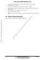
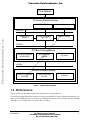
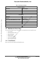
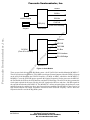
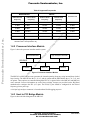
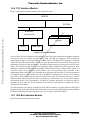
Freescale Semiconductor, Inc.
MPC105EVB/D
(Motorola Order Number)
7/94
,I
R
TO
C
U
N
D
Advance Information
SE
M
IC
O
MPC603/MPC604 Evaluation System—
Big Bend Technical Summary
R
C
H
IV
ED
B
Y
FR
EE
SC
A
LE
This document describes an evaluation system that demonstrates the capabilities of two
PowerPC™ microprocessors—the MPC603 or MPC604. The system, named Big Bend, is
a PowerPC Reference Platform (PReP) compliant design. The motherboard inside the Big
Bend system is an 8-layer PCB design, baby AT-size (9-inch x 13-inch) form factor, and
uses the MPC105 processor to PCI bridge device for core logic. Other major components
on the motherboard include the UMC PCI-ISA bridge, National Semiconductor’s Super
I/O controllers, and NCR’s SCSI controller. Big Bend provides an example that can be used
in designing other systems using PowerPC microprocessors. In addition to the Big Bend
evaluation system, an evaluation kit containing design information and a manufacturing kit
containing in-depth manufacturing information are available.
1.1 System Features
The main features of the Big Bend system are as follows:
•
PReP compliant MPC603/MPC604 evaluation system
•
Desktop system in baby AT form factor
•
Supports MPC603 and MPC604 with external bus speeds up to 66 MHz
•
Processor to PCI bridge with Motorola MPC105
•
PCI to ISA bridge with UMC UM8886
•
Onboard National Semiconductor PC87323 super I/O chip supports two 16550
serial ports, one parallel port, floppy, keyboard, mouse, and IDE interface
PowerPC, PowerPC 604, and PS/2 are trademarks of International Business Machines Corp. used by Motorola under license from IBM Corp. and
Windows NT is a trademark of Microsoft Corporation.
This document contains information on a new product under development. Specifications and information herein are subject to change without notice.
© Motorola Inc. 1994
For More Information On This Product,
Go to: www.freescale.com
Big Bend Technical Summary
A
Freescale Semiconductor, Inc...
N
C
.
™
Freescale Semiconductor, Inc.
•
Onboard NCR53C825 SCSI controller to support the SCSI hard drive and CD ROM
•
High performance PCI graphics
•
Second-level cache selectable between 256 Kbyte, 512 Kbyte or 1 Mbyte
•
Supports onboard DRAM up to 128 Mbyte; support for 4-Mbyte, 8-Mbyte, 16-Mbyte, and 32Mbyte SIMMs
•
Three 16-bit ISA bus slots and three 32-bit PCI bus slots
•
Standard 101 PS/2™-style keyboard
•
Supplied with Windows NT™ operating system and selected applications pre-installed on hard
drive
.
C
N
,I
R
C
H
IV
ED
B
Y
FR
EE
SC
A
LE
SE
M
IC
O
N
D
U
C
TO
R
Figure 1 shows the block diagram for the Big Bend motherboard:
A
Freescale Semiconductor, Inc...
1.2 System Block Diagram
2
Big Bend Technical Summary
For More Information On This Product,
Go to: www.freescale.com
MOTOROLA
Freescale Semiconductor, Inc.
Clock Module
Processor Interface Module
MPC603/MPC604
Logic Analyzer Connector
N
,I
Host to PCI Bridge
MPC105
TO
R
Memory Module
D
U
C
Cache Memory
Module
M
IC
O
N
PCI BUS
LE
SE
PCI Bus Interface Module
PCI-ISA Bridge
UM8886
PCI Slots
FR
EE
SC
A
PCI SCSI Controller
NCR53C825
ED
B
Y
ISA BUS
R
C
H
IV
ISA Bus Interface Module
Super I/O Controller
PC87323
A
Freescale Semiconductor, Inc...
C
.
60X BUS
Real Time Clock
DS1387
ISA Slots
Figure 1. System Block Diagram
1.3 Performance
The key goal for the Big Bend design is high performance at a reasonable cost.
The following timing indicates the number of clock cycles the MPC105 takes for different operations. It is
based on the 66-MHz processor bus frequency, 33-MHz PCI frequency, 64-bit 60X bus and 60-ns DRAM
and 1 Mbyte of L2 cache with a 9-ns access time; see Table 1.
MOTOROLA
Big Bend Technical Summary
For More Information On This Product,
Go to: www.freescale.com
3
Freescale Semiconductor, Inc.
Table 1. Performance Analysis
Processor to Memory
L2 Cache Hit
Number of Cycles
Burst read
3-1-1-1
Burst write
3-1-1-1
Read followed by pipelined write
3-1-1-1-2-1-1-1
Burst write
2-1-1-1-1-1-1-1
On-Chip Cache (MPC603/MPC604) and L2 Miss
Number of Cycles
Burst read
9-1-1-1-1-1-1-1
Burst write
2-1-1-1-1-1-1-1
C
Number of Cycles
,I
R
TO
C
U
D
N
O
IC
SE
M
Processor to PCI
12-2-2-2
EE
SC
1.4 Hardware Overview
A
LE
Burst read
Y
H
IV
ED
B
Clock module
Processor interface module
Host to PCI bridge
Memory module
Cache memory module
PCI bus interface module
ISA bus interface module
R
C
•
•
•
•
•
•
•
FR
The system block diagram shown in Figure 1 has seven modules that are now described in turn.
A
Freescale Semiconductor, Inc...
N
L2 Cache Hit
.
PCI to Memory
1.4.1 Clock Module
Figure 2 shows the clock module on the Big Bend system.
4
Big Bend Technical Summary
For More Information On This Product,
Go to: www.freescale.com
MOTOROLA
Freescale Semiconductor, Inc.
14 MHz
24 MHz
14-MHz Crystal
128 KHz
SYSCLK
FSEL(0:2)
(From 25 to 66 MHz)
AV9154-06
,I
R
TO
IC
O
N
D
U
C
Processor
TAG RAM
PCI Bus
SCSI Interface
PCI-ISA Bridge
MC88PL117
Figure 2. Clock Module
IV
ED
B
Y
FR
EE
SC
A
LE
SE
M
SYSCLK
(From 25 to 66 MHz)
MPC105
R
C
H
There are two clock drivers on the Big Bend system—the ICS AV9154-06 and the Motorola MC88PL117.
The AV9154-06 uses an external 14.31818 MHz crystal input. External jumpers tied to the FSEL(0:2) inputs
on the AV9154-06 determine the SYSCLK frequency (25 MHz–66 MHz), which drive the MC88PL117.
MC88PL117 uses the SYSCLK input to generate the required frequencies for the processor, the MPC105,
the TAG RAM, the PCI bus, the SCSI interface, and the PCI-ISA bridge. The AV9154-06 also generates the
clock signal required for the super I/O chip, the OSC signal on the ISA bus, and also a 128-KHz signal for
the suspend refresh mode of the MPC105. The MC88PL117 utilizes an internal phase-locked loop to create
multiple frequencies, and has low-skew, large fan-out driving capability. The MC88PL117 has a total of 14
high current outputs with output frequencies referenced to the SYSCLK frequency. Table 2 shows the
frequencies that are used in the Big Bend system.
A
Freescale Semiconductor, Inc...
N
C
.
Jumpers
MOTOROLA
Big Bend Technical Summary
For More Information On This Product,
Go to: www.freescale.com
5
Freescale Semiconductor, Inc.
Table 2. Supported Frequencies
MPC603/MPC604
External Clock
Frequency
MPC105
Internal Clock
Frequency
External Clock
Frequency
Internal Clock
Frequency
PCI Bus Clock
40 MHz
80 MHz
20 MHz
40 MHz
20 MHz
25 MHz
75 MHz1
25 MHz
25 MHz
25 MHz
33 MHz
66 MHz
33 MHz
33 MHz
33 MHz
33 MHz
66 MHz
33 MHz
MHz2
100
66 MHz
66 MHz
33 MHz
66 MHz
66 MHz
100 MHz
33 MHz
66 MHz
PowerPC 604™ microprocessor only
C
N
,I
R
TO
80-MHz processor operating at 75 MHz
2
33 MHz
N
D
U
C
1
33MHZ
M
LE
SE
Figure 3 shows the processor interface module system.
IC
O
1.4.2 Processor Interface Module
Logic Analyzer Connector
EE
SC
A
MPC603/MPC604
MPC105
Memory
R
C
H
IV
L2 Cache
ED
B
Y
FR
60X BUS
Figure 3. Processor Interface Module
A
Freescale Semiconductor, Inc...
.
33 MHz
The MPC603 or MPC604 processor generates the internal operating frequency using internal phase-locked
loop circuitry. The MPC603 has the x1, x2, x3, and x4 options and the MPC604 has the x1, x1.5, x2, and
x4 options. These options are controlled through the PLL (0:3) signals. Refer to the MPC603 and MPC604
user’s manuals for more information on each of these settings. Jumpers are provided on the Big Bend
motherboard to configure the PLL (0:3) pins. The PLL(0:3) pins should be configured for the desired
frequency prior to power-up.
A 160-pin logic analyzer connector is located onboard for debugging purposes.
1.4.3 Host to PCI Bridge Module
Figure 4 shows the block diagram of the MPC105.
6
Big Bend Technical Summary
For More Information On This Product,
Go to: www.freescale.com
MOTOROLA
Freescale Semiconductor, Inc.
60X Bus Interface
Memory Controller
JTAG Interface
Cache Controller
,I
R
N
D
U
C
TO
PCI Interface
IC
O
Figure 4. MPC105 Block Diagram
ED
B
Y
FR
EE
SC
A
LE
SE
M
The MPC105 is the single-chip PReP compliant bridge device providing access between the
MPC603/MPC604 processor and the PCI bus. MPC105 also integrates a secondary cache controller and a
high performance memory controller that supports DRAM or SDRAM, and ROM or Flash ROM. In the Big
Bend design, up to 128 Mbytes of onboard DRAM and 1 Mbyte of Flash ROM are supported. The
MPC105’s processor interface module handles the processor transactions and performs snoop operations.
This interface also provides the bus arbitration function between the processors, one level of address
pipelining, and address and data bus parking. The secondary cache controller supports 256 Kbyte to 1 Mbyte
of direct-mapped cache in write-through or write-back mode; either mode can be programmed through an
internal configuration register. For performance reasons, Big Bend supports the write-back mode as the
default.
R
C
H
IV
The MPC105 starts both secondary cache and memory accesses in parallel to reduce secondary cache miss
latency. The memory cycle is aborted if there is a hit on the second-level cache. Nonpipelined burst
transactions can be completed with a timing of 3-1-1-1 clock cycles. Pipeline burst can be completed with
timing of 2-1-1-1 clock cycles. The cache controller interfaces with external TAG RAM and synchronous
RAM. Programmable timing is provided to suit various system requirements.
A
Freescale Semiconductor, Inc...
N
C
.
PLL
The JTAG interface on the MPC105 provides a boundary-scan capability for board testing. The MPC105
provides all the test port signals required by the IEEE 1149.1 boundary-scan specification. For more
information about JTAG, refer to the IEEE 1149.1 document.
1.4.4 Memory Interface Modules
Figure 5 shows the memory module on the Big Bend system.
MOTOROLA
Big Bend Technical Summary
For More Information On This Product,
Go to: www.freescale.com
7
Freescale Semiconductor, Inc.
MPC603/MPC604
Address
Data
A
D
Control
N
,I
MA
MD
C
TO
R
Flash ROM
IC
O
N
D
U
MPC105
SE
M
MA
LE
RAS, WE
36-Bit SIMM
FR
EE
SC
A
CAS
B
Y
Figure 5. Memory Module on Big Bend
R
C
H
IV
ED
The MPC105’s memory interface module is designed to support DRAM or synchronous DRAM as main
memory. Big Bend supports 4 banks of DRAM with a maximum of 128 Mbytes when using 16-Mbit RAM.
Bidirectional buffers are needed on the data bus. The enable and direction control are managed by the
MPC105. Buffers are added on all the MA, RAS and WE signals. The MPC105 supports normal CAS
before RAS refresh. In sleep mode, the MPC105 uses the 128-KHz clock as a refresh time base. The best
case access timing using 60-ns DRAMs at 66 MHz is 7-3-3-3 clock cycles.
A
Freescale Semiconductor, Inc...
C
.
Buffers
The MPC105’s memory interface module is also designed to support ROM or Flash ROM on either the 60X
bus or the PCI bus. Big Bend supports Flash ROM for easy code update. A 512-Kbyte Flash ROM is located
on the 60X Bus.
1.4.5 Cache Memory Module
Figure 6 shows the cache memory module on the Big Bend system.
8
Big Bend Technical Summary
For More Information On This Product,
Go to: www.freescale.com
MOTOROLA
Freescale Semiconductor, Inc.
IDT71216
TAG RAMS
A0-A31
MPC105
RESET
RES
A
TWE
WE
TOE
OE
C
.
D
N
DIRTY_O
,I
TO
R
Q
C
HIT
U
D0-D63
N
D
DIRTY_I
M
IC
O
PAL (22V10)
SE
SYS_CLK
LE
A29-A31
TBST
TSIZ0-TSIZ2
ADSC
DWE
TALE
WE0-WE7
CS0-CS1
SC
IV
ED
B
Y
FR
EE
ADS
DWE
TALE
A
TBST
TSIZ(0..2)
H
DOE
R
C
BAA
BURST
SRAMS
MCM72MA64
WE0-WE7
CS0-CS1
A
SYSCLK
BAA
A
Freescale Semiconductor, Inc...
MATCH
OE
D(0..63)
Figure 6. Cache Memory Module
Big Bend supports cache sizes from 256 Kbyte to 1 Mbyte. The cache interface circuitry inside the MPC105
is designed to run at 66 MHz. IDT 71216 16K x 15 TAG RAMs and Motorola MCM72MA64 burst SRAMs
are used as the data synchronous RAM. The access time is 10 ns for TAG RAM and 9 ns for the data
SRAMs. Big Bend supports both write-back and write-through direct-mapped operation. The fastest
nonpipelined burst cycle is 3-1-1-1 while the timing for pipelined bursts is 2-1-1-1. The MPC105 provides
four signals for interfacing the synchronous burst SRAMs. External logic (22V10 PAL) is required in the
Big Bend system to decode which bytes of the 64-bit double word should be selected for the write by
decoding the A29–A31, TBST, and the TSIZ0–TSIZ2 signals. Currently, parity on the secondary-level
cache is not supported.
MOTOROLA
Big Bend Technical Summary
For More Information On This Product,
Go to: www.freescale.com
9
Freescale Semiconductor, Inc.
1.4.6 PCI Interface Module
Figure 7 shows the PCI interface module on the Big Bend system.
MPC105
PCI BUS
C
.
NCR53C825
N
,I
R
TO
IC
WIDE SCSI
SE
M
SCSI II
O
N
D
U
C
PCI Slots
A
LE
Figure 7. PCI Interface Module
R
C
H
IV
ED
B
Y
FR
EE
SC
There are three PCI slots available on the Big Bend system. One slot is dedicated to the graphics controller
card and two slots are available for other add-on cards. The MPC105 supports a 32-bit multiplexed,
address/data bus that can run from 20 MHz to 33 MHz (Table 2). The MPC105 PCI interface is compliant
with the PCI Local Bus Specification, revision 2.0. It also provides buffers between the PCI bus, processor,
and memory to improve system performance. The MPC105 implements two 16-byte processor-to-PCI write
buffers. These buffers are split to allow the store gathering function defined in the PCI specification. Store
gathering is important for high performance graphic frame buffer operations in which a whole sequence of
consecutive writes can be generated by the software. One 32-bit processor-to-PCI read buffer is also
implemented. Data in this buffer is not forwarded to the processor until the buffer is full or the transaction
is completed. Between system memory and PCI, the MPC105 implements two 32-byte PCI-to-memory
write buffers. These buffers hold two cache lines so that back-to-back writes from PCI may occur, with PCI
filling one buffer while the data in the other is forwarded to system memory. One 32-byte PCI-to-memory
read prefetch buffer is also implemented. The MPC105 supports speculative read operation while it
prefetches the next cache line at the completion of the first PCI read operation to enhance the PCI-tomemory read performance.
A
Freescale Semiconductor, Inc...
SCSI Controller
The SCSI interface is provided by an NCR53C825 PCI SCSI controller. It supports both the 8-bit SCSI II
interface and the 16-bit wide SCSI interface (both connectors are located on the Big Bend system). Both the
CD ROM and the hard disk in the Big Bend system are accessed via the SCSI interface.
1.4.7 ISA Bus Interface Module
Figure 8 shows the ISA bus interface module.
10
Big Bend Technical Summary
For More Information On This Product,
Go to: www.freescale.com
MOTOROLA
Freescale Semiconductor, Inc.
PCI Bus
PCI-ISA Controller
UM 8886
ISA Bus
C
Parallel
U
IDE
Keyboard
SE
M
Mouse
ISA Slots
A
LE
Floppy
IC
O
N
D
Serial
TO
R
,I
N
C
.
RTC
DS1387
EE
SC
Figure 8. ISA Bus Interface Module
H
IV
ED
B
100% PCI and ISA compatible
Incorporates two 8237 DMA controllers
High performance PCI arbiter
Incorporates two 8259 interrupt controllers
One 82C54 16-bit counter/timer
R
C
•
•
•
•
•
Y
FR
Big Bend uses the UMC UM8886 PCI-ISA controller as a bridge to the ISA bus. The UM8886 provides the
following functions:
A
Freescale Semiconductor, Inc...
Super I/O Controller
PC87323
Big Bend uses the National PC87323 super I/O controller to provide the functionality of two(16550 UARTcompatible) serial ports, one bidirectional parallel port, an 8042 compatible keyboard controller, a PS/2style keyboard and mouse interface, an 82077 compatible floppy disk controller interface, and an IDE
interface.
The PC87323 is connected to the ISA bus.
The real time clock function is provided by the Dallas Semiconductor DS1387 controller. It also contains a
4K nonvolatile RAM for storing system configuration data.
Three ISA slots are located on the Big Bend system. Each can support a standard 8-bit or 16-bit ISA addon card.
MOTOROLA
Big Bend Technical Summary
For More Information On This Product,
Go to: www.freescale.com
11
Freescale Semiconductor, Inc.
1.5 Firmware
The Big Bend firmware is provided by the Motorola RISC Software division. The firmware performs the
following tasks:
C
.
Initializes chipset registers
Tests motherboard hardware
Performs memory sizing
Initializes the interrupt controller
Configures the PCI interface card
Initializes console to text mode
Initializes boot device
Loads and executes the OS loader
,I
C
TO
R
1.6 System Configuration
N
O
IV
ED
B
Y
FR
EE
SC
A
LE
SE
M
IC
80-MHz MPC603 PowerPC microprocessor
32-Mbyte memory on board
3.5-inch and 5.25-inch diskette drives
500-Mbyte SCSI hard drive
CD ROM drive with SCSI II interface
Windows accelerated video card w/4-Mbyte VRAM
Ethernet card
Baby-AT desktop case
Three 16-bit ISA slots
Three PCI slots
PS/2-style keyboard and mouse
Windows NT operating system pre-installed
R
C
H
•
•
•
•
•
•
•
•
•
•
•
•
D
U
The following list provides the standard system configuration for Big Bend:
1.7 Documentation
A
Freescale Semiconductor, Inc...
N
•
•
•
•
•
•
•
•
Big Bend is shipped with an evaluation kit and a manufacturing kit, which contain the following
documentation:
The evaluation kit contains the following documents:
•
•
•
•
•
•
•
12
MPC105 technical summary
MPC603 power management application note
MPC603 technical summary
MPC604 technical summary
Big Bend technical summary
Bill of materials
Schematics—hard copy
Big Bend Technical Summary
For More Information On This Product,
Go to: www.freescale.com
MOTOROLA
Freescale Semiconductor, Inc.
The manufacturing kit contains the following documents:
N
C
.
MPC105 user’s manual
MPC603/MPC604/MPC105 errata sheets
Artwork—hard copy
Ball-grid array socket information
Big Bend user’s manual
Board layout and wiring guidelines
Data sheets for other components
Gerber file
PReP specification
Schematics—soft copy
Schematics component library—soft copy
A
R
C
H
IV
ED
B
Y
FR
EE
SC
A
LE
SE
M
IC
O
N
D
U
C
TO
R
Freescale Semiconductor, Inc...
,I
•
•
•
•
•
•
•
•
•
•
•
MOTOROLA
Big Bend Technical Summary
For More Information On This Product,
Go to: www.freescale.com
13
,I
R
TO
C
U
D
N
O
IC
M
SE
LE
A
SC
EE
FR
Y
B
ED
Information in this document is provided solely to enable system and software implementers to use PowerPC microprocessors. There are no express or implied
copyright licenses granted hereunder to design or fabricate PowerPC integrated circuits or integrated circuits based on the information in this document.
R
C
H
IV
Motorola reserves the right to make changes without further notice to any products herein. Motorola makes no warranty, representation or guarantee regarding
the suitability of its products for any particular purpose, nor does Motorola assume any liability arising out of the application or use of any product or circuit, and
specifically disclaims any and all liability, including without limitation consequential or incidental damages. “Typical” parameters can and do vary in different
applications. All operating parameters, including “Typicals” must be validated for each customer application by customer’s technical experts. Motorola does not
convey any license under its patent rights nor the rights of others. Motorola products are not designed, intended, or authorized for use as components in
systems intended for surgical implant into the body, or other applications intended to support or sustain life, or for any other application in which the failure of
the Motorola product could create a situation where personal injury or death may occur. Should Buyer purchase or use Motorola products for any such
unintended or unauthorized application, Buyer shall indemnify and hold Motorola and its officers, employees, subsidiaries, affiliates, and distributors harmless
against all claims, costs, damages, and expenses, and reasonable attorney fees arising out of, directly or indirectly, any claim of personal injury or death
associated with such unintended or unauthorized use, even if such claim alleges that Motorola was negligent regarding the design or manufacture of the part.
Motorola and
are registered trademarks of Motorola, Inc. Motorola, Inc. is an Equal Opportunity/Affirmative Action Employer.
A
Freescale Semiconductor, Inc...
N
C
.
Freescale Semiconductor, Inc.
IBM is a registered trademark of IBM Corp.
, PowerPC, and PowerPC 604 are trademarks of International Business Machines Corp. used by
Motorola under license from IBM Corp; PS/2 is a trademark of IBM Corporation; and Windows NT is a trademark of Microsoft Corporation.
Motorola Literature Distribution Centers:
USA: Motorola Literature Distribution, P.O. Box 20912, Phoenix, Arizona 85036.
EUROPE: Motorola Ltd., European Literature Centre, 88 Tanners Drive, Blakelands, Milton Keynes, MK14 5BP, England.
JAPAN: Nippon Motorola Ltd., 4-32-1, Nishi-Gotanda, Shinagawa-ku, Tokyo 141 Japan.
ASIA-PACIFIC: Motorola Semiconductors H.K. Ltd., Silicon Harbour Centre, No. 2 Dai King Street, Tai Po Industrial Estate,
Tai Po, N.T., Hong Kong.
Technical Information: Motorola Inc. Semiconductor Products Sector Technical Responsiveness Center; (800) 521-6274.
Document Comments: FAX (512) 891-2638, Attn: RISC Applications Engineering.
For More Information On This Product,
Go to: www.freescale.com