1
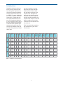
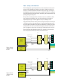
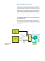
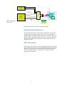
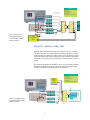
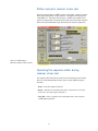
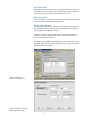
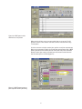
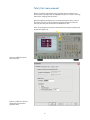
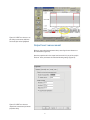
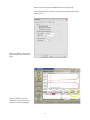
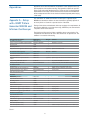
Agilent
Method of Implementation (MOI) for
DisplayPort Sink Compliance Test
Application Note
Overview
This method of implementation (MOI) document explains how to perform the sink compliance tests as
described in the VESA DisplayPort Compliance Test Specification (CTS) version 1.1 draft 12.
This group of tests verifies receiver functionality under stressed-signal conditions, for the purposes of performing DisplayPort Interoperability Testing. This test is limited to functionalities which are covered by the CTS,
and do not provide comprehensive coverage of all receiver tolerance requirements defined by the DisplayPort
Standard v1.1 specification. However the same or similar procedures may be the basis for more rigorous testing
and product characterization.
This document will first explain the test requirements and procedures in a generic way. Subsequent chapters
will add instrument specific operation procedures when using J-BERT N4903A high-performance serial BERT
to implement the test.
Table of Contents
Overview .......................................................................................................................1
Table of Contents ........................................................................................................2
Introduction..................................................................................................................3
Basic Requirements ...................................................................................................7
Calibration Procedure.................................................................................................7
Test Procedure.............................................................................................................8
J-BERT N4903A Stressed Signal Generator ........................................................11
Signal Calibration with J-BERT Error Detector....................................................17
Appendices ................................................................................................................23
Appendix A - Setup with J-BERT Pattern Generator N4903A
and Infiniium Oscilloscope .....................................................................................23
Appendix B - J-BERT N4903A Setup ....................................................................24
Appendix C - Setup with ParBERT 81250 Pattern Generator
and Infiniium Oscillocope .......................................................................................25
Appendix D - ParBERT 81250 Setup ......................................................................27
Related Literature ....................................................................................................28
2
Introduction
DisplayPort sink devices have one,
two or four high speed serial data
lanes. During sink compliance test
all lanes will be tested sequentially.
The test pattern for the stress test
is a PRBS 2^7-1 pattern. Additionally
the CTS details specific amounts of
random jitter, sinusoidal jitter and
inter symbol interference for each
test case. Therefore the definitions
in the CTS involve two major steps in
the sink compliance test procedure:
a calibration of the impaired signal
and the actual receiver stress test.
For both steps different setups will
be needed and operation procedures
will be given.
f(Sj)
TP2
RBR
TP2
HBR
TP3
RBR
TP3
HBR
Data rate
(GB/s)
Tj
(mUI)
ISI
(mUI)
Rj
(RMS)
(mUI)
2
1,620000
1178
100
7,9
10
1,620567
308
100
7,9
Rj
(p-p)
(mUI)
The setup calibration is typically
done once prior to test execution.
Calibration data will be recorded
and used when running the actual
compliance test. During the test
phase each lane will be tested individually while the remaining lanes
basically stay idle. Nevertheless the
compliance test comprises cross talk
effects by sending a clock pattern
to the lanes that are adjacent to the
lane under test.
Table 1 summarized the compliance
test requirements as given in the
CTS document.
Sj
(mUI)
Signal
voltage (eye
opening at
50%) (mV)
97,17
981
400
97,17
111
400
Signal edge
rate (ps)
(20/80)
Aggressor
voltage (eye
opening at
50%) (mV)
Attenuator with
J-BERT
(dB)
Aggressor edge
rate [ps]
(20/80)
Aggressor
frequency
(MHz)
Max no. of
allowable bit
errors (1)
Observation time
(s)
50-130
1200
2
130
405,00000
1000
620
50-130
1200
2
130
405,14175
100
62
20
1,620000
277
100
7,9
97,17
80
400
50-130
1200
2
130
405,00000
100
62
2
2,700000
1062
144
13,2
162,4
756
350
50-130
1050
2
130
675,00000
1000
370
10
2,700945
492
144
13,2
162,4
186
350
50-130
1050
2
130
675,23625
100
37
20
2,700000
472
144
13,2
162,4
166
350
50-130
1050
2
130
675,00000
100
37
100
2,700000
467
144
13,2
162,4
161
350
50-130
1050
2
130
675,00000
100
37
2
1,620000
1648
570
7,9
97,17
981
46
50-130
138
15
130
405,00000
1000
620
10
1,620567
778
570
7,9
97,17
111
46
50-130
138
15
130
405,14175
100
62
20
1,620000
747
570
7,9
97,17
80
46
50-130
138
15
130
405,00000
100
62
2
2,700000
1079
161
13,2
162,4
756
150
50-130
450
4
130
675,00000
1000
370
10
2,700945
509
161
13,2
162,4
186
150
50-130
450
4
130
675,23625
100
37
20
2,700000
489
161
13,2
162,4
166
150
50-130
450
4
130
675,00000
100
37
100
2,700000
484
161
13,2
162,4
161
150
50-130
450
4
130
675,00000
100
37
Table 1. Compliance test requirements
3
Test setup calibration
The CTS defines the signal impairment for the sink compliance test at specific
test points (TP). Depending on whether a sink with a receptacle connector is
tested or a sink with a tethered cable different test points apply. According to
the DisplayPort standard these test points are either TP2 or TP3. The calibration
setup and procedures ensure the correct amounts of jitter and the minimum eye
opening at the given test point.
TP2 and TP3 are usually part of the sink device and not accessible for calibration. Therefore the calibration setup uses two test fixtures to measure the
required signals. Figure 1 shows a generic setup for calibrating at TP3.
A plug test fixture drives the stress pattern (in the given example on lane 0) into
a receptacle test fixture for measurements. A stressed signal generator sends
the stress pattern that will be measured and calibrated at TP3 with a jitter measurement device. A clean i.e. jitter free clock signal is the basis for the calibrations. The aggressor signals are just driven into 50 Ohm termination resistors.
Figure 2 illustrates the calibration setup for TP2. Generally it is the same but
uses a receptacle test fixture to connect the sink device later.
TP3’
Stress
pattern
Clean
clock
signal
Figure 1. Generic
calibration setup
for TP3
Aux
L3
L2
L1
Test fixture
Stressed
signal
generator
+
+
+
+
+
-
Test fixture
Aggressor signal
(clock pattern)
TP3
L0
Plug
fixture
Receptacle
fixture
50 Ω
50 Ω
50 Ω
50 Ω
Legend
TP: test point
Jitter
measurement
device
TP2’
Stress
pattern
Clean
clock
signal
Aux
L3
L2
L1
L0
Receptacle
fixture
Test fixture
Stressed
signal
generator
+
+
+
+
+
-
TP2
Test fixture
Aggressor signal
(clock pattern)
Figure 2. Generic
calibration setup
for TP2
Aux +
L3 +
L2 +
L1 +
L0 +
-
Aux +
L3 +
L2 +
L1 +
L0 +
-
Plug
fixture
50 Ω
50 Ω
50 Ω
50 Ω
Legend
TP: test point
Jitter
measurement
device
4
Basic compliance test setup
Once the setup is completely calibrated the calibration test fixture with the jitter
measurement device is disconnected and the remaining test fixture with the
stressed signal generator connected will be connected to the device under test.
According to the DisplayPort standard all sink devices integrate a PRBS7 error
counter. This counter is used during the compliance test to capture bit errors.
The counter can be read and controller in using the auxiliary channel. Therefore the recommended procedure is to utilize an auxiliary channel controller for
reading the counter. This controller may also serve to execute the test itself as it
involves some reading and writing of DisplayPort control registers.
If such a controller isn’t available or a sink device doesn’t support the auxiliary
channel some other proprietary means may be used to control the sink device
and read the PRBS7 counter.
Figure 3 shows a typical setup for testing a sink device with a receptacle connector. The auxiliary channel controller is connected to the test fixture. Even if
not shown above the auxiliary channel controller may remain connected during
setup calibration too.
Auxiliary
channel
controller
TP3‘
Stressed
signal
generator
Stress
pattern
Figure 3. Generic test
setup for TP3
+
+
+
+
+
-
Aux
L3
L2
L1
Test fixture
Aggressor signal
(clock pattern)
TP3 TP4
Receiver
PRBS7
counter
L0
Plug
fixture
Legend
TP: test point
5
DUT device
under
test
Auxiliary
channel
controller
TP2‘
Stressed
signal
generator
Figure 4. Generic test
setup for TP2
Stress
pattern
+
+
+
+
+
-
TP3 TP4
Aux
L3
L2
L1
Test fixture
Aggressor signal
(clock pattern)
TP2
Receiver
Display port
cable
L0
Receptacle
fixture
DUT device
under
test
PRBS7
counter
Legend
TP: test point
Figure 4 shows testing of a sink device with tethered cable.
Supported test equipment
This application note supports a variety of test equipment for stressed signal
generator and for the jitter measurement device. This includes the Agilent
J-BERT N4903A, the ParBERT 81250A, and Infiniium oscilloscopes. No specific
auxiliary channel controller will be mentioned here. The appendices at the end
of the document detail possible combinations of test equipment and list all
required accessories.
Test automation
All procedures of the compliance test as well as additional product characterization can be performed automatically with the N5990A test automation software.
Agilent offers a DisplayPort option that supports the equipment listed above.
The test automation software is not required and it is shown as optional
equipment in the appendices.
6
Basic Requirements
To follow the procedures laid out here it is required to be familiar with the compliance test specification (CTS) and the DisplayPort Standard as well as with the
used equipment. Make sure that you have the user’s manuals and the standards
documents available.
Auto calibration of instruments
Before starting with any of the procedures in this document perform an auto
calibration of the used instruments. With J-BERT open the self-test dialog from
the utility menu and perform a PG and if applicable an ED auto calibration. With
ParBERT for each clock group use the user software and execute a delay auto
calibration from the system menu. If an oscilloscope is used for setup calibration, follow the instrument calibration description in the user’s manual.
Always terminate generator outputs
Regardless whether J-BERT or ParBERT is used as stressed signal generator ensure that the high speed outputs (i.e. clock and data) are always terminated with
50 Ohms. This can be done with 50 Ohm termination resistors or by connecting
the outputs to either the device under test or to a measurement device. Refer to
the user’s manuals for further details.
De-skew the setup
When using non-matched pair cables considerable skew may be introduced
to the setup. Either individually measure and match the cables before setup or
check the complete setup for differential skew later. Make sure that minimum
skew is introduced at the test point.
Calibration
Procedure
This chapter generically explains how to calibrate the setup without addressing
instrument specific details. Refer to Table 1 for the target values for calibration.
1.
Setup the stressed signal generator and the jitter measurement device for
calibration
2. Set the desired data rate and start with a high signal amplitude
3. Turn off or disconnect the aggressor signals
4. Configure the stressed signal generator to send a half rate clock pattern
(“11001100…”)
5. Calibrate Rj with Sj turned off
6. Turn on or connect the aggressor signals
7. Configure the stressed signal generator to send a PRBS 2^7-1 pattern
8. Measure Tj
9. Calculate Sj for all frequencies as Sj(f) = Target Tj(f) – measured Tj
10. Set Sj(20 MHz)
11. Measure the eye opening and adjust the generator output amplitude to
achieve the required minimum eye opening
7
Test Procedure
The test procedure requires the operation of the device under test and refers to
the auxiliary channel and internal DPCD registers. In order to execute the test
procedure either an auxiliary channel controller or some proprietary test tool is
required.
Figure 5 shows a GUI example of an auxiliary channel test tool. The left area
shows the DPTC register map and the controls on the right side allow reading
and writing individual registers.
Figure 5. GUI of an auxiliary
channel test tool example
The following procedure has to be followed for each lane, all supported data
rates and all sinusoidal jitter frequencies that have to be tested for each supported data rate.
The aggressor signals have to be connected in the following order:
•
Device under test has one lane:
No aggressor signal connected.
Turn off or disconnect the aggressor signals
•
Device under test has two lanes:
Test lane 0: connect aggressor to lane 1
Terminate the other aggressor signal with 50 Ohm
Test lane 1: connect aggressor to lane 0
Terminate the other aggressor signal with 50 Ohm
•
Device under test has four lanes:
Test lane 0: connect aggressor to lane 1 and 3, lane 2 is not connected
Test lane 1: connect aggressor to lane 0 and 2, lane 3 is not connected
Test lane 2: connect aggressor to lane 1 and 3, lane 0 is not connected
Test lane 3: connect aggressor to lane 0 and 2, lane 1 is not connected
8
Set up your test equipment for sink testing. Load the required pattern files to the
BERT sequencer. Have the previously measured calibration data ready.
1. Write LINK_BW_SET (address 0x100) and LANE_COUNT_SET (address
0x101)
2. Connect the stressed signal generator to the lane under test and the aggressor signals to the adjacent lanes. Adjust data rates for Reduced Bit Rate or
High Bit Rate. All jitter sources and minimum eye were calibrated previously
and are turned on
Frequency lock phase
3. The stressed signal generator outputs a D10.2 clock pattern to the lane under
test (includes injected ISI, Rj and Sj jitter).
4. The auxiliary channel controller initiates the frequency lock phase and disables scrambling by writing TRAINING_PATTERN_SET (address 0x102 bits 5,
1:0)
5. After >100μs the auxiliary channel controller verifies whether the DUT
achieved frequency lock. If not go to the previous step. If frequency lock
cannot be achieved within 5 retries (with maximum consecutive AUX Defers
allowable = 8) the test result shall be a failure. Lock is verified by polling
CR_LOCK status for the data lane under test:
If LANE0_CR_DONE (Address202h bit 0) = 1
If LANE1_CR_DONE (Address202h bit 4) = 1
If LANE2_CR_DONE (Address203h bit 0) = 1
If LANE3_CR_DONE (Address203h bit 4) = 1
Symbol Lock Phase
6. The stressed signal generator outputs symbol lock pattern as defined in
specification with ISI, Rj and SJ jitter injected
7. The auxiliary channel controller Control initiates the symbol lock phase and
disables scrambling by writing TRAINING_PATTERN_SET (address 0x102 bits
5, 1:0)
8. After >100μs AUX Control verifies whether DUT achieved symbol lock. If not
go to the previous step. If symbol lock cannot be achieved within 5 retries
(with maximum consecutive AUX Defers allowable = 8) the test result will be
a failure. Lock is verified by polling CR_LOCK status for the data lane under
test:
If LANE0_CHANNEL_EQ_DONE (Address202h bit 1)
If LANE0_SYMBOL_LOCKED (Address202h bit 2)
If LANE1_CHANNEL_EQ_DONE (Address202h bit 5)
If LANE1_SYMBOL_LOCKED (Address202h bit 6)
If LANE2_CHANNEL_EQ_DONE (Address203h bit 1)
If LANE2_SYMBOL_LOCKED (Address203h bit 2)
If LANE3_CHANNEL_EQ_DONE (Address203h bit 5)
If LANE3_SYMBOL_LOCKED (Address203h bit 6)
PRBS7 counter test phase
9. The stressed signal generator outputs a PRBS 2^7-1 pattern as defined in
specification with ISI, Rj and SJ jitter injected
10. The auxiliary channel controller initiates and clears the PRBS7 error counter
by the following procedure:
(a) set TRAINING_PATTERN_SET (address 0x102, bits 1:0) to training not in
progress
(b) set TRAINING_PATTERN_SET (address 0x102, bits 3:2) to PRBS7
transmitted
(c) clear the error counter by reading SYMBOL_ERROR_COUNT_LANEx for
lane x under test (address 0x210, 0x211 for lane 0, address 0x212, 0x213
for lane 1, address 0x214, 0x215 for lane 2, address 0x216, 0x217 for lane 3)
9
11. The stressed signal generator injects a random number of errors (for example number of errors, n, be a number from 1 to 10) while looping the PRBS
pattern. (I.e. for first n repetitions of the PRBS7 pattern one error is injected
and subsequent PRBS patterns no errors are injected)
12. AUX Control verifies that the PRBS7 error counter shows n or more errors. If
not the test result will be a failure. (Note: due to the impaired signal conditions during link training the receiver may see more bit errors)
BER test phase
13. The stressed signal generator outputs a PRBS 2^7-1 pattern as defined in
specification with Rj, Sj, and ISI jitter injected
14. The auxiliary channel controller clears the PRBS7 error counter by reading SYMBOL_ERROR_COUNT_LANEx for lane x under test (address 0x210,
0x211 for lane 0, address 0x212, 0x213 for lane 1, address 0x214, 0x215 for
lane 2, address 0x216, 0x217 for lane 3)
15. Run test for specified time
16. The PRBS7 error counter is read through the auxiliary channel controller
by reading SYMBOL_ERROR_COUNT_LANEx for lane x under test (address
0x210, 0x211 for lane 0, address 0x212, 0x213 for lane 1, address 0x214,
0x215 for lane 2, address 0x216, 0x217 for lane 3)
Prepare next test
17. Turn off test pattern by set TRAINING_PATTERN_SET (address 0x102, bits
3:2) to link quality test pattern not transmitted
Pass/fail criteria
For each lane and all supported data rates:
• The device under test is required to achieve frequency lock and symbol lock
within 5 retries
• The PRBS7 counter has to be operational and must count no fewer than
injected number of errors during the counter test
• The number of bit errors during the BER test doesn’t exceed the given limit
in Table 1 for stressed signal testing
10
J-BERT N4903A
Stressed Signal
Generator
This chapter provides the details that are needed to perform the setup calibration and test execution as described before when using J-BERT as the stressed
signal generator.
Clock settings
Set the clock rate of the J-BERT patter generator to the desired data rate. For
testing at RBR the data rate is 1.62Gb/s and 2.7Gb/s for testing at HBR. Please
keep in mind that some of the compliance tests add an offset to the data rate.
Refer to the requirements given in Table 1.
J-
Figure 6. J-BERT pattern
generator bit rate setup menu
BERT’s trigger and sub rate clock outputs are used to generate the aggressor
signal that will be sent to the lanes which are adjacent to the lane under test.
In order to generate a half rate clock signal set sub rate clock divider to 4 (as
shown in Figure 6) and the trigger output to clock divided by 4 as shown in
Figure 7.
Figure 7. J-BERT pattern generator
trigger output setup window
11
Initial output amplitude
For initial jitter calibration, a high generator amplitude is recommended. Set the
pattern generator output to 1V. Later this setting will be calibrated to the desired
eye opening.
Figure 8. J-BERT pattern generator
output levels setup menu
Output amplitude modification
Either use the pattern generator output setup menu or the front panel knob as
shown in Figure 9.
Figure 9. J-BERT pattern
generator front panel with
output level knob highlighted
12
Jitter settings
In the jitter setup, enable the jitter generation and random jitter as well as periodic jitter. Switch the upper delay line (500 ps or 600 ps depending on J-BERT
configuration) to periodic jitter. Further select the sinusoidal modulation for periodic jitter. Enter the frequency of the periodic jitter and the amplitude of random
as well as periodic jitter in the jitter submenus. Initially set the amplitude for
periodic jitter to zero.
Figure 10. J-BERT pattern
generator jitter setup menu
External wiring for aggressor signal
With the J-BERT pattern generator three different setup configurations will be
used for the aggressor signals.
When calibrating the random jitter the aggressor signals are generally disconnected. The figure below further uses the test fixtures in a configuration to
calibrate to TP3. If a device with tethered cable (i.e. calibration to TP2) shall
be tested only the order of the plug fixture and the receptacle fixture has to be
changed.
13
Legend
Attn: attenuator
PD: power divider
BC: blocking capacitor
TP: test point
TTC: 150 ps transition time converter
TP3‘
TTC BC ISI-Gen
Figure 11. Setup For Rj
calibration with J-BERT
pattern generator
Jitter
measurement
device
Stress
pattern
L3
L2
L1
Test fixture
Aux
Test fixture
+
+
+
+
+
-
TTC BC ISI-Gen
Clean
clock
signal
TP3
L0
Plug
fixture
Aux +
L3 +
L2 +
L1 +
L0 +
-
50 Ω
50 Ω
50 Ω
50 Ω
Receptacle
fixture
In order to calibrate the total jitter for TP3 (see section on setup calibration) the
aggressor signals must be connected (Figure 11). Use attenuators to adjust the
amplitude. When testing at RBR 15dB will be needed. When testing at HBR 4dB
will be needed.
Legend
Attn: attenuator
PD: power divider
BC: blocking capacitor
TP: test point
TTC: 150 ps transition time converter
TP3‘
TP3
Aggressor signal
(clock pattern)
TTC
TTC
Figure 12. Setup
for Tj and amplitude
calibration at TP3 with
J-BERT pattern generator
Jitter
measurement
device
BC
BC
BC
+
+
+
+
+
-
PD
PD
ISI-Gen
ISI-Gen
Stress
pattern
Clean
clock
signal
Aux
L3
L2
L1
L0
Plug
fixture
Test fixture
TTC Attn
BC
Test fixture
TTC Attn
Aux +
L3 +
L2 +
L1 +
L0 +
-
50 Ω
50 Ω
50 Ω
50 Ω
Receptacle
fixture
Testing a sink device with tethered cable requires calibration of TP2 (Figure
13). In order to achieve the amplitude requirements for the aggressor signal
no power dividers can be used. The trigger and the sub-rate clock outputs will
generate the same half rate clock signal. Using both as shown below with 2 dB
attenuators will result in the required amplitude.
14
Legend
Attn: attenuator
PD: power divider
BC: blocking capacitor
Aggressor signal
(clock pattern)
TP: test point
TTC: 150 ps transition time converter
TTC Attn
BC
TP2‘
TTC Attn
BC
TTC Attn
BC
TTC
TTC
Figure 13. Setup for Tj
and amplitude calibration at TP2 with J-BERT
pattern generator
Jitter
measurement
device
BC
BC
+
+
+
+
+
-
ISI-Gen
ISI-Gen
Stress
pattern
Clean
clock
signal
Aux
L3
L2
L1
Test fixture
BC
Test fixture
TTC Attn
TP2
L0
50 Ω
Aux +
L3 +
L2 +
L1 +
L0 +
-
50 Ω
50 Ω
50 Ω
Plug
fixture
Receptacle
fixture
Setup for receiver stress test
Figure 14 shows the principle setup for stress testing lane 0 of a sink device.
The aggressor signals are connected like for total jitter calibration. The figure
shows the setup for testing at TP3. When testing at TP2 the aggressor signal
and the test fixture setup change analogously to the calibration setup. Before
starting the actual receiver stress test the jitter measurement device is disconnected.
Test operation and reading of the PRBS7 counter can be done with proprietary
debug tools. However the usage of a standards compliant auxiliary channel
controller as indicated in the setup below is recommended.
Legend
Attn: attenuator
PD: power divider
BC: blocking capacitor
Auxiliary
channel
controller
TP: test point
TTC: 150 ps transition time converter
TP3 TP4
TP3‘
Aggressor signal
(clock pattern)
BC
PD
TTC Attn
BC
PD
TTC
BC
ISI-Gen
TTC
BC
ISI-Gen
+
+
+
+
+
-
Stress
pattern
15
Aux
L3
L2
L1
L0
Plug
fixture
Test fixture
Figure 14. Compliance test
setup with Agilent J-BERT
pattern generator
TTC Attn
Receiver
PRBS7
counter
DUT device
under
test
Pattern setup for receiver stress test
Open the sequence editor in J-BERT’s pattern menu. Define a sequence of three
blocks with the DisplayPort training sequence 1, DisplayPort training sequence
2 and PRBS 2^7-1. The pattern files are given in J-BERT’s demo folder for DisplayPort. Configure block one and two to be looped until manual break and block
three to be looped indefinitely. Figure 15 illustrates the required configuration.
Figure 15. J-BERT pattern
generator sequence editor controls
Operating the sequence editor during
receiver stress test
The sequence editor indicates the active block in the lower left corner with B1,
B2, or B3. The following features will be used to control J-BERT during test
execution:
• Reset – resets the sequence to block 1.
• Break – switches from one block to the next, i.e. from block 1 to 2 or from
block 2 to 3. Use reset to go back to block 1.
• Error Add – inserts a single bit error to the pattern that is sent out by the
J-BERT pattern generator.
16
Signal Calibration
With J-BERT N4903A
Error Detector
Figure 16 shows the required cabling when using the J-BERT error detector as a
jitter measurement device. It includes the cabling for stressed signal generation
by J-BERT.
Note: it isn’t a requirement to generate the stressed signal by J-BERT when using J-BERT’s error detector as a jitter measurement device.
Connect the clean clock signal provided by the stressed signal generator to the
clock input of the error detector. Connect the stress pattern from the desired
test point to the error detector’s data input.
Legend
Attn: attenuator
PD: power divider
BC: blocking capacitor
TP: test point
TTC: 150 ps transition time converter
TP3‘
TP3
Aggressor signal
(clock pattern)
PD
TTC Attn
BC
PD
TTC
TTC
BC
BC
+
+
+
+
+
-
ISI-Gen
ISI-Gen
Stress
pattern
Aux
L3
L2
L1
L0
Plug
fixture
Test fixture
BC
Test fixture
TTC Attn
Aux +
L3 +
L2 +
L1 +
L0 +
-
50 Ω
50 Ω
50 Ω
50 Ω
Receptacle
fixture
Figure 16. Calibration setup
when using J-BERT for jitter
and amplitude calibration
Note: the figure above illustrates the use of J-BERT’s error detector when calibrating at TP3. Analogously the error detector can be used to calibrate at TP2.
Figure 17 shows the equipment to calibrate the J-BERT stressed signal generator with the J-BERT error detector.
Figure 17. Sample calibration setup
17
Clock input setting
Make sure that the error detector clock is connected to the pattern generator
clock output and the pattern generator clock amplitude is sufficient (Figure 18).
In the error detector user interface select external clock source.
Data input setting
In the error detector’s sampling point setup menu choose edit to open the input
setup dialog. Select differential signaling (Figure 19).
Random jitter calibration
The random jitter calibration has to be performed without the cross talk effects
from the aggressor signals. Refer to the stressed signal generator chapter for
setup configuration and generator settings.
Configure the stressed signal generator to send a half rate clock pattern (i.e.
11001100…). Make sure that the same pattern is programmed to the error
detectors expected pattern memory.
For example use the J-BERT’s pattern editor (as shown in Figure 20) to create
the desired 4 bit pattern and use the “To PGED” button to send it to the pattern
generator and the error detector.
Figure 18. J-BERT error
detector clock setup menu
Figure 19. J-BERT error detector
input setup dialog settings
18
Figure 20. J-BERT pattern editor
with half rate clock pattern
Make sure that all jitter sources except random jitter are set to zero. The ISI
generator remains connected but no ISI effects will be measured when using
a clock pattern.
In order to measure and adjust random jitter, perform a total jitter measurement.
Refer to next paragraph for details on the total jitter measurement. With J-BERT
pattern generator use the random jitter tab in the jitter setup menu and iterate
between random jitter settings and total jitter measurement until the desired
level of random jitter is achieved (Figure 21).
Figure 21. J-BERT pattern generator
jitter setup with random jitter dialog
19
Total jitter measurement
Before a total jitter measurement always auto align the error detector. Press
the front panel auto align button as highlighted in Figure 22 or use the auto align
button in the sampling point setup menu.
Open the properties tab (Figure 23) in the output timing menu which is part of
the analysis functions. In the parameters tab set the resolution to 1mUI and
select the fast total jitter measurement at a BER level of 1E-9.
Press the start button to execute the measurement and read the total jitter peak
to peak value (Figure 24).
Figure 22. J-BERT front panel
auto align button
Figure 23. J-BERT error detector
output timing measurement
properties dialog
20
Figure 24. J-BERT error detector output timing measurement with measured total jitter value highlighted
Output level measurement
Before an output level measurement always auto align the error detector as
described before (Figure 24).
Open the properties tab in the output level menu which is part of the analysis
functions. In the parameters tab make the following settings (Figure 25).
Figure 25. J-BERT error detector
output level measurement parameter
properties dialog
21
Switch to the view tab and set the BER threshold to 1E-9 (Figure 26).
Press the start button to execute the measurement and read threshold margin
value (Figure 27).
Figure 26. J-BERT error detector output level measurement view options
dialog
Figure 27. J-BERT error detector
output level measurement with eye
opening measurement highlighted
22
Appendices
Appendix A – Setup
with J-BERT Pattern
Generator N4903A and
Infiniium Oscilloscope
Appendixes A to D describe different combinations of test equipment that support DisplayPort sink compliance testing. The appendices explain the specifics
of the setups and provide detailed part lists. These part lists are the equipment
requirements for the setup covered. Some listed accessories are bundled with
the test equipment and thus do not need to be ordered separately when buying
a new setup.
The combination of J-BERT and Infiniium oscilloscope is supported by the
N5990A test automation software. As test automation is generally optional all
necessary items are shown in a separate section of the table.
Testing of sink devices with tethered cable may not always be a requirement. As
this requires additional accessories when using J-BERT they are summarized in
a separate section of the table too.
The Infiniium oscilloscope has further capabilities to test source devices. For
completeness the table lists the source test software as an optional item. This
software is not used for sink testing.
Signal generation and calibration
Model number
7G J-BERT pattern generator
N4903A-G07, J10
No. of units
1
Comments
Infiniium oscilloscope with 8GHz or higher bandwidth
DSA80000 or DSA90000
1
Differential probe
1169A
1
Differential probe head
5380A
1
DisplayPort source test application software for scope
U7232A
1 (optional)
Optional transmitter test suite
No. of units
Comments
DSA90000 recommended
Test automation software (optional)
Model number
Test automation software platform core product
N5990A-010
DisplayPort receiver test
N5990A-155
1
DisplayPort interface to scope transmitter test
software
N5990A-255
1 (optional)
Laptop including PCMCIA IEEE 1394 card
81250A-015
1
Only needed with N5990A test automation
LAN hub (includes five LAN cables)
Bitifeye BIT-GEN-NCK-001
1
3rd party product. Only needed with N5990A test automation software
Plug test fixture
W2641A
1
Includes 4 pairs of straight SMP to SMA cables
90° SMP to SMA cables (recommended only)
E4809-61603
8
N5460A matched pair alternative, 4 pairs needed
Receptacle test fixture for setup calibration
Bitifeye BIT-DP-RTF-0001
1
3rd party product
SMA cable kit (includes 4 cables)
15442A
2
1
Optional support for transmitter measurements with scope only
Test fixtures and cables
Accessories
Display port ISI generator
N4915A-006
1
150 ps transition time converter
15435A
4
DC blocking capacitor
N9398C
4
Power divider
11636B
2
50 Ohm termination resistors
1250-2206
4
4 dB attenuator for aggressor signal at HBR, TP3
Mini Circuits BW-S4W2+
2
3rd party product
5 dB attenuator for aggressor signal at RBR, TP3
Mini Circuits BW-S5W2+
2
3rd party product
10 dB attenuator for aggressor signal at RBR, TP3
Mini Circuits BW-S10W2+
2
3rd party product
150 ps transition time converter
15435A
2
DC blocking capacitor
N9398C
2
2 dB attenuator for aggressor signal at RBR/HBR, TP2
Mini Circuits BW-S2W2+
4
Additional accessories for TP2
SMA (f) to SMA (f)
1250-1158
4
SMA cable kit (includes 4 cables)
15442A
1
SMA cable kit (includes 4 cables)
15442A
1
Table A-1.
23
3rd party product
15443A matched pair alternative, replace one set of 15442A by two
Appendix B. J-BERT
N4903A Setup
Testing of sink devices with tethered cable may not always be a requirement. As
this requires additional accessories when using J-BERT they are summarized in
a separate section of the table.
Signal generation
and calibration
Model number
No. of units
Comments
7G J-BERT
N4903A-C07, J10
Test fixtures & cables
Model number
Plug test fixture
W2641A
1
Includes 4 pairs of straight SMP to SMA
cables
90° SMP to SMA cables
(recommended only)
E4809-61603
8
N5460A matched pair alternative, 4 pairs
needed
Receptacle test fixture for setup
calibration
BitifEye BIT-DP-RTF-0001,
3rd party product
1
3rd party product
1
No. of units
SMA cable kit (includes 4 cables) 15442A
Comments
2
Accessories
Display port ISI generator
N4915A-006
1
150 ps transition time converter
15435A
4
DC blocking capacitor
N9398C
4
Power divider
11636B
2
50 Ohm termination resistors
1250-2206
4
4 dB attenuator for aggressor
signal at HBR, TP3
Mini Circuits BW-S4W2+
2
3rd party product
5 dB attenuator for aggressor
signal at RBR, TP3
Mini Circuits BW-S5W2+
2
3rd party product
10 dB attenuator for aggressor
signal at RBR, TP3
Mini Circuits BWS10W2+
2
3rd party product
150 ps transition time converter
15435A
2
DC blocking capacitor
N9398C
2
2 dB attenuator for aggressor
signal at RBR/HBR, TP2
Mini Circuits BW-S2W2+
4
SMA (f) to SMA (f)
1250-1158
4
Additional accessories for TP2
SMA cable kit (includes 4 cables) 15442A
1
Table B-1.
24
3rd party product
15443A matched pair alternative, replace
one set of 15442A by two sets of 15443A
Appendix C.
Setup with
ParBERT 81250A
Pattern Generator
and
Infiniium Oscillocope
The combination of J-BERT and Infiniium oscilloscope is supported by the
N5990A test automation software. As test automation is generally optional all
necessary items are shown in a separate section of the table.
The Infiniium oscilloscope has further capabilities to test source devices. For
completeness the table lists the source test software as an optional item. This
software is not used for sink testing.
The ParBERT setup may be used for DisplayPort and for HDMI. As testing for
HDMI requires more ParBERT generators as DisplayPort these generators would
simplify cabling and eliminate some accessories for the DisplayPort setup. The
comment section of Table C-1 (see next page) highlights the differences.
25
Signal generation
and calibration
Model number
No. of units
Central clock
E4909A
2
7G generator
N4874A
2
ParBERT mainframe
81250A-149
1
IEEE 1394 PC link to VXI
81250A-013
1
ParBERT 81250 software license
E4875A
1
Laptop including PCMCIA IEEE
1394 card
81250A-015
1
81150A with two channels
81150A-002
1
Signal generator
E4438C, Options 503, 601
UNJ -or- N5182A-654
1
Infiniium oscilloscope with
8GHz or higher bandwidth
DSA80000 or DSA90000
1
Differential probe
1169A
1
Differential probe head
5380A
1
DisplayPort source test
application software for scope
U7232A
1 (optional)
LAN hub
(includes five LAN cables)
Bitifeye BIT-GEN-NCK-001
Test automation software
(optional)
Model number
Test Automation Software
Platform Core Product
N5990A option 010
1
DisplayPort receiver test
N5990A option 155
1
DisplayPort interface to scope
transmitter test software
N5990A option 255
1 (optional)
Test fixtures & cables
Model number
Plug test fixture
W2641A
1
Includes 4 pairs of straight SMP to SMA
cables
90° SMP to SMA cables
(recommended only)
E4809-61603
8
N5460A matched pair alternative,
4 pairs needed
Receptacle test fixture for setup
calibration
BitifEye BIT-DP-RTF-0001,
3rd party product
1
3rd party product
3
15443A matched pair alternative, replace
one set of 15442A by two sets of 15443A
1
No. of units
No. of units
SMA cable kit (includes 4 cables) 15442A
Comments
3 generators also supported by N5990A
DSA90000 recommended
Optional transmitter test suite
3rd party product
Comments
Optional support for transmitter
measurements with scope only
Comments
Accessories
2.4 mm to 3.5 mm adapters
11901C
8
12 if 3 generators are used
50 Ohm termination resistors
1250-2206
8
10 if 3 generators are used
Power divider
11636B
2
Not needed if 3 generators are used
Adapter n to 3.5 mm (f)
1250-1744
1
DC blocking capacitor
N9398C
4
6 if 3 generators are used
150 ps transition time converter
15435A
4
6 if 3 generators are used
Display port ISI generator
N4915A-006
1
BNC to SMA adapter
1250-2015
1
SMA (f) to SMA (f)
1250-1158
4
Table C-1.
26
Appendix D.
ParBERT 81250
Setup
The ParBERT setup may be used for DisplayPort and for HDMI. As testing for
HDMI requires more ParBERT generators as DisplayPort these generators would
simplify cabling and eliminate some accessories for the DisplayPort setup. The
comment section of the table highlights the differences.
No. of
units
Signal generation and calibration
Model number
Central clock
E4909A
2
7G generator
N4874A
2
7G analyzer
N4875A
1
ParBERT mainframe
81250A-149
1
IEEE 1394 PC link to VXI
81250A-013
1
ParBERT 81250 software license
E4875A
1
Laptop including PCMCIA IEEE
1394 card
81250A-015
1
81150A with two channels
81150A-002
1
Signal generator
E4438C, Options 503, 601
UNJ
-orN5182A-654
2
LAN hub (includes 5 LAN cables)
BitifEye BIT-GEN-NCK0001, 3rd party product
1
Test fixtures & cables
Model number
Plug test fixture
W2641A
1
Includes 4 pairs of straight SMP to SMA
cables
90° SMP to SMA cables
(recommended only)
E4809-61603
8
N5460A matched pair alternative,
4 pairs needed
Receptacle test fixture for setup
calibration
BitifEye BIT-DP-RTF-0001,
3rd party product
1
3rd party product
3
15443A matched pair alternative, replace
one set of 15442A by two sets of 15443A
No. of
units
SMA cable kit (includes 4 cables) 15442A
No. of
units
Comments
If 3 generators are available some
accessories may be saved.
Comments
Accessories
Model number
2.4 mm to 3.5 mm adapters
11901C
10
14 if 3 generators are used
50 Ohm termination resistors
1250-2206
8
10 if 3 generators are used
Power divider
11636B
2
Not needed if 3 generators are used
Adapter n to 3.5 mm (f)
1250-1744
2
DC blocking capacitor
N9398C
4
6 if 3 generators are used
150 ps transition time converter
15435A
4
6 if 3 generators are used
Display port ISI generator
N4915A-006
1
BNC to SMA adapter
1250-2015
1
BNC to BNC cable
8120-1839
1
Table D-1.
27
Comments
Related Literature
Title
Pub number or
web address
VESA DisplayPort Standard, Version 1.1
www.vesa.org
VESA DisplayPort PHY Compliance Test Standard,
Version 1.1, Draft 12
www.vesa.org
Agilent ParBERT 81250 Parallel Bit Error Ratio Tester
- Product Overview V 5.66
5968-9188E
Agilent J-BERT N4903A High-Performance Serial BERT
5989-2899EN
Agilent Technologies Infiniium DSO/DSA 90000A Series
Real-Time Oscilloscope
5989-7819EN
Agilent N4915A-006 DisplayPort ISI Generator
5989-8688EN
Agilent W2641A DisplayPort Test Point Access Adapter
5989-7274EN
RF & Microwave Test Accessories Catalog 2006/07
5968-4314EN
Test Automation Software Platform N5990A
5989-5483EN
BitifEye Test Fixture
www.bitifeye.com
Mini Circuits Attenuators
www.minicircuits.com
Remove all doubt
Our repair and calibration services
will get your equipment back to you,
performing like new, when promised. You will get full value out of
your Agilent equipment throughout its lifetime. Your equipment
will be serviced by Agilent-trained
technicians using the latest factory
calibration procedures, automated
repair diagnostics and genuine parts.
You will always have the utmost
confidence in your measurements.
Agilent offers a wide range of additional expert test and measurement services for your equipment,
including initial start-up assistance,
onsite education and training, as
well as design, system integration,
and project management.
For more information on repair and
calibration services, go to:
www.agilent.com/find/removealldoubt
Agilent Email Updates
www.agilent.com/find/emailupdates
Get the latest information on the
products and applications you select.
Agilent Direct
www.agilent.com/find/agilentdirect
Quickly choose and use your test
equipment solutions with confidence.
Agilent
Open
www.agilent.com/find/open
Agilent Open simplifies the process
of connecting and programming
test systems to help engineers
design, validate and manufacture
electronic products. Agilent offers
open connectivity for a broad range
of system-ready instruments, open
industry software, PC-standard I/O
and global support, which are
combined to more easily integrate
test system development.
www.agilent.com
www.agilent.com/find/dp_rx_test
For more information on Agilent Technologies’ products, applications or services,
please contact your local Agilent office.
The complete list is available at:
www.agilent.com/find/contactus
Americas
Canada
Latin America
United States
(877) 894-4414
305 269 7500
(800) 829-4444
Asia Pacific
Australia
China
Hong Kong
India
Japan
Korea
Malaysia
Singapore
Taiwan
Thailand
1 800 629 485
800 810 0189
800 938 693
1 800 112 929
0120 (421) 345
080 769 0800
1 800 888 848
1 800 375 8100
0800 047 866
1 800 226 008
Europe & Middle East
Austria
0820 87 44 11
Belgium
32 (0) 2 404 93 40
Denmark
45 70 13 15 15
Finland
358 (0) 10 855 2100
France
0825 010 700*
*0.125 €/minute
Germany
01805 24 6333**
**0.14 €/minute
Ireland
Israel
Italy
Netherlands
Spain
Sweden
Switzerland
United Kingdom
1890 924 204
972-3-9288-504/544
39 02 92 60 8484
31 (0) 20 547 2111
34 (91) 631 3300
0200-88 22 55
0800 80 53 53
44 (0) 118 9276201
Other European Countries:
www.agilent.com/find/contactus
Revised: March 27, 2008
Product specifications and descriptions in this document subject to
change without notice.
© Agilent Technologies, Inc. 2008
Published in USA, August 18, 2008
5989-9147EN