1
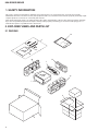
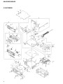
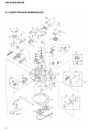
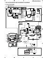
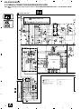
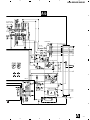
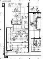
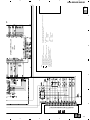
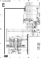
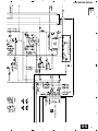
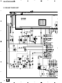
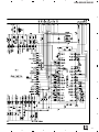
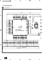
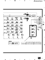
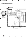
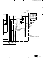
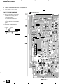
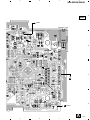
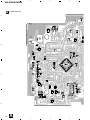
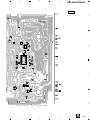
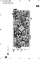
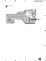
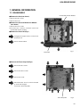
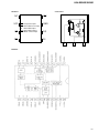
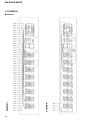
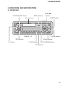
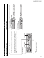
Service Manual KEH-3930R/X1M/EW ORDER NO. CRT2420 HIGH POWER CASSETTE PLAYER WITH RDS TUNER KEH-3930R KEH-3900R X1M/EW X1M/EW - This service manual should be used together with the following manual(s): Model No. CX-1011 Order No. CRT2406 Mech. Module Remarks 3L Cassette Mech. Module:Circuit Description, Mech.Description, Disassembly CONTENTS 1. 2. 3. 4. 5. 6. SAFETY INFORMATION ............................................2 EXPLODED VIEWS AND PARTS LIST .......................2 BLOCK DIAGRAM AND SCHEMATIC DIAGRAM .....9 PCB CONNECTION DIAGRAM ................................22 ELECTRICAL PARTS LIST ........................................32 ADJUSTMENT..........................................................36 7. GENERAL INFORMATION .......................................37 7.1 DISASSEMBLY ...................................................37 7.2 PARTS .................................................................38 7.2.1 IC................................................................38 7.2.2 DISPLAY ....................................................42 8. OPERATIONS AND SPECIFICATIONS.....................43 PIONEER CORPORATION 4-1, Meguro 1-Chome, Meguro-ku, Tokyo 153-8654, Japan PIONEER ELECTRONICS SERVICE INC. P.O.Box 1760, Long Beach, CA 90801-1760 U.S.A. PIONEER ELECTRONIC [EUROPE] N.V. Haven 1087 Keetberglaan 1, 9120 Melsele, Belgium PIONEER ELECTRONICS ASIACENTRE PTE.LTD. 253 Alexandra Road, #04-01, Singapore 159936 C PIONEER CORPORATION 1999 K-ZZD. NOV. 1999 Printed in Japan KEH-3930R,3900R 1. SAFETY INFORMATION This service manual is intended for qualified service technicians; it is not meant for the casual do-it-yourselfer. Qualified technicians have the necessary test equipment and tools, and have been trained to properly and safely repair complex products such as those covered by this manual. Improperly performed repairs can adversely affect the safety and reliability of the product and may void the warranty. If you are not qualified to perform the repair of this product properly and safely, you should not risk trying to do so and refer the repair to a qualified service technician. 2. EXPLODED VIEWS AND PARTS LIST 2.1 PACKING 12 4 3 2 5 6 10 13 1 11 7 9 8 2 KEH-3930R,3900R NOTE: - Parts marked by “*” are generally unavailable because they are not in our Master Spare Parts List. - Screws adjacent to ∇ mark on the product are used for disassembly. (1) PACKING SECTION PARTS LIST Mark No. Description 1 2 3 4 5 * 6 7 8 9 10 Part No. Cord Assy Accessory Assy Screw Handle Bush CDE6100 CEA1917 CBA1304 CNC5395 CNV3930 Polyethylene Bag Polyethylene Bag Carton Contain Box Protector E36-615 CEG-162 See Contrast table(2) See Contrast table(2) Mark No. Description * * 11 12-1 12-2 12-3 12-4 Protector Owner’s Manual Owner’s Manual Installation Manual Passport 12-5 Warranty Card 12-6 Polyethylene Bag 13 Case Assy Part No. CHP2244 CRD3122 CRD3123 CRD3124 CRY1013 CRY1157 CEG1116 CXB3520 CHP2243 (2) CONTRAST TABLE KEH-3930R/X1M/EW and KEH-3900R/X1M/EW are constructed the same except for the following: Part No. Mark No. Symbol and Description KEH-3930R/X1M/EW KEH-3900R/X1M/EW 8 Carton CHG3844 CHG3843 9 Contain Box CHL3844 CHL3843 - Owner's Manual, Installation Manual Model KEH-3930R/X1M/EW KEH-3900R/X1M/EW Part No. CRD3122 CRD3123 CRD3124 Language English, Spanish, German French, Italian, Dutch English, Spanish, German, French, Italian, Dutch 3 KEH-3930R,3900R 2.2 EXTERIOR 4 KEH-3930R,3900R (1) EXTERIOR SECTION PARTS LIST Mark No. Description 1 2 3 4 5 Part No. Mark No. Description Part No. Screw Screw Screw Cord Assy Plug BSZ26P050FMC BSZ30P050FMC BSZ30P200FMC CDE6100 CKM1314 31 32 33 34 35 Screw Button(DETACH) Button(1-6) Button(EJECT) Button(+ -) BPZ20P100FZK 6 7 8 9 10 Case Earth Plate Spacer Insulator Tuner Amp Unit CNB2350 CNC8368 CNM4913 CNM5963 CWM6806 36 37 38 39 40 Button(SELECT) Button(SOURCE/LOUD) Spring Cover Keyboard Unit See Contrast table(2) 11 12 13 14 15 Screw Screw Cord FM/AM Tuner Unit Holder BSZ26P080FMC BSZ26P160FMC CDE6158 CWE1500 CNC7532 41 42 43 44 45 LCD(LCD1801) Connector(CN1801) Holder Rubber Lighting Conductor CAW1559 CKS3580 CNC8517 CNV5954 CNV6274 16 17 18 19 20 Plug(CN604) Connector(CN602) Connector(CN601) Antenna Jack(CN402) Panel CKM1288 CKS3568 CKS3581 CKX1056 CNB2344 46 47 48 49 50 Rubber Grille Unit Button Spring Spring CNV5968 21 22 23 24 25 Holder Holder Holder Holder Insulator CNC5399 CNC6845 CNC7533 CNC7996 CNM5967 51 52 53 54 55 Spring Bracket Bracket Arm Arm CBH2182 CNC6135 CNC6791 CNV4692 CNV4693 26 27 28 29 30 Heat Sink Holder Unit ••••• Chassis Unit Detach Grille Assy CNR1505 CXB2687 56 57 58 59 60 Arm Panel Unit Door Spring Screw 61 62 63 64 65 Screw Fuse(10A) IC(IC302) Transistor(Q904) See Contrast table(2) See Contrast table(2) See Contrast table(2) CAC6275 CAC6277 See Contrast table(2) CAC6494 CBH2210 See Contrast table(2) See Contrast table(2) See Contrast table(2) CAC4836 CBH1834 CBH1835 CNV4728 See Contrast table(2) See Contrast table(2) CBH1838 IMS20P030FZK Cassette Mechanism Module EXK4100 ISS26P055FUC CEK1136 TDA7384 2SD2396 (2) CONTRAST TABLE KEH-3930R/X1M/EW and KEH-3900R/X1M/EW are constructed the same except for the following: Mark No. 29 30 32 35 36 39 40 47 57 58 Symbol and Description Chassis Unit Detach Grille Assy Button(DETACH) Button(+ -) Button(SELECT) Part No. KEH-3930R/X1M/EW KEH-3900R/X1M/EW CXB4530 CXB4529 CXB4850 CXB4849 CAC5929 CAC5789 CAC6458 CAC6273 CAC6459 CAC6276 Cover Keyboard Unit Grille Unit Panel Unit Door CNS5662 CWM6813 CXB5840 CXB4929 CAT2108 CNS5661 CWM6812 CXB4519 CXB4928 CAT2109 5 KEH-3930R,3900R 2.3 CASSETTE MECHANISM MODULE 6 KEH-3930R,3900R - CASSETTE MECHANISM MODULE SECTION PARTS LIST Mark No. Description Part No. Mark No. Description Part No. 1 2 3 4 5 Screw Washer Washer Screw Screw BSZ20P040FMC CBF1037 CBG1003 EBA1028 CBA1037 46 47 48 49 50 Pinch Roller Pinch Holder Unit Pinch Roller Reel Unit Head Base Unit ENV1518 EXA1583 ENV1518 EXA1585 EXA1586 6 7 8 9 10 Spring Spring Spring Spring Spring EBH1531 EBH1624 EBH1625 EBH1626 EBH1627 51 52 53 54 55 Lever Unit Gear Unit Motor Unit(Service) Washer Screw EXA1587 EXA1588 EXX1055 HBF-179 CBA1250 11 12 13 14 15 Spring Cord Photo-reflector(EGN1) Arm Lever EBH1628 EDD1024 EGN1004 ENC1526 ENC1530 56 Bracket 16 17 18 19 20 Lever Arm Frame Holder Gear ENC1531 ENC1532 ENC1533 ENC1534 ENC1535 21 22 23 24 25 Arm Roller Belt Collar Arm ENC1536 ENR1040 ENT1027 ENV1508 ENV1539 26 27 28 29 30 Arm Gear Gear Gear Worm Wheel ENV1540 ENV1544 ENV1547 ENV1548 ENV1550 31 32 33 34 35 Lever Flywheel Gathering PCB Switch(S1,S2) Deck Unit ENV1551 ENV1554 ENX1054 ESG1007 EWM1023 36 37 38 39 40 Plug(CN251) Gathering PCB Motor Unit(M1) Motor Head Assy(HD1) CKS3540 ENX1053 EXA1491 EXM1028 EXA1592 41 42 43 44 45 Motor Unit(M2) Screw Bracket Chassis Unit Pinch Holder Unit EXA1580 BMZ20P022FMC ENC1528 EXA1582 EXA1584 ENC1542 7 KEH-3930R,3900R 8 1 3 2 4 KEH-3930R,3900R 3. BLOCK DIAGRAM AND SCHEMATIC DIAGRAM 3.1 BLOCK DIAGRAM A TUNER AMP UNIT FM/AM 1ST IF 10.7MHz T51 Q51 CF51 CF52 CF53 FM FRONT END Q3 39 42 44 46 63 Q903 46 VDD B.U LDET TMUTE 54 COMP 78 LDET 21 Q476 18 65 71 35 33 32 45 55 57 28 CF202 61 74 75 SYSPW EEPROM 5 AM RF AM 2ND IF 450kHz Q202 IC 3 BR9010FV 6 4 RDS DECODER 3 VDD LOCL NL2 NL1 FMSD 2 21 FM/AM 3 IC 701 PM4009A 20 4 SWVDD 24 NL1 SDBL CE1 SL 13 SD 8 SDBW TUNPCE PCE2 PDIO 12 15 16 SL CK CE2 DI/DO 22 10 14 Q411 TUNPCK 25 61 51 VDD VCC 55 Q477 11 X702 PDIO TAPE-L 3 IC301 SN761029DL B CN604 POWER AMP 11 15 Q350 IC302 TDA7384 FL RL MUTE MUTE 9 FL- 7 RL- 19 RL+ 17 STBY 22 FL+ 2 1 B5 B6 FL+ FL- 8 B8 7 B7 RLRL+ 4 Q351 Q352 Q904 VCC IC601(1/2) PE5088A 20 RL FL 19 VCK/VDT/VST 2 SYSTEM CONTROLLER TUN-L ELECTRONIC VOLUME TUN-L TMUTE 68 74 FM/AM 78 NL1 53 SD 76 SL 10 SDBW 14 TUNPCE 13 TUNPCK 20 PCE2 12 TUNPDO 11 TUNPDI 28 LOCL 12 VDD VCC LDET VDD RF TV ANT2 TV 6 70 MIXER.IF AMP DET IC 1 PML002A Q201 Q204 Q474 TUNER Lch 19 IC 2 PM4008A 34 33 41 44 11 12 13 69 22 Q472 24 32 2 38 A FM MPX 25 27 AVDD CN401 1 ANT1 TV SYSPW B.U 13 FUSE 10A Q901 BSENS A4 BACK UP A7 ACC Q905 VDD D DECK UNIT 2 STBY 7 8 10 20 20 19 19 11 11 LOAD 3 1 5 6 3 1 5 6 RIMUTE 30 RIMUTE B.U STBY 48 42 LD STBY LOADSW CN602 X2 IC601(2/2) PE5088A 63 CN256 X601 SYSTEM CONTROLLER TELIN B.REMOTE 69 TEL MUTE 64 TEL MUTE 8 9 5 VDD EGN1 REEL SENSE A S1 LOAD E REEL SENSE PCB SWVDD Q650 VDD SWITCH SW5V ILL S2 MODE CN901 Q951 SW5V 17 CN253 C 70 KYDT CN255 SYSPW A5 POWER SWITCH 1 IC901 6 TPD1018F CN601 8 7 3 4 5 8 7 3 4 5 C KEYBOARD UNIT CN1801 VDD 50 10 18 DPDT 20 KYDT VLCD 19 18 IC351 PA2020A 9 DPDT B.U 9 SWVDD D LCD DRIVER IC1801 PD6293A KEY MATRIX LCD XI XO M 66 65 60 X1 MUTE MECHANISM DRIVER 2 1 5 2 1 M1 MAIN MOTOR 54 ASENS Lch 10 DSENS M 3 17 CN254 M2 SUB MOTOR 3 LOUT 7 11 Q906 VCC DPDT 4 4 KYDT REV L-ch IC251 CXA2559Q TAPE+B 4 RESET 37 36 39 5 5 ACC ASENS SYSPW CN251 EQ AMP B.U 1 IC602 S-80834ANY DSENS FWD L-ch Q902 A BSENS CN252 1 8.4V REGULATOR RESET MUTE ANTENNA JACK FM/AM TUNER UNIT SYSPW B 23 22 X901 9 1 2 3 4 2 1 3 4 KEH-3930R,3900R 3.2 OVERALL CONNECTION DIAGRAM(GUIDE PAGE) Note: When ordering service parts, be sure to refer to “EXPLODED VIEWS AND PARTS LIST” or “ELECTRICAL PARTS LIST”. A A A-a A-b TUNER AMP UNIT B A-a A-a A-b A-b A-a ANTENNA JACK Large size SCH diagram FM/AM TUNER UNIT SOUR ELECT Guide page FM(100%) : -15.5dBs AM(30%) : -26dBs Detailed page FM AM TA B RESET RDS DECODER SYSTEM CONTROLLER PE5088A C D 10 A 1 TAPE 315Hz(0dB) : -7.9dBs CASSETTE MECHANISM MODULE D E NOTE : Symbol indicates a resistor. No differentiation is made between chip resistors and discrete resistors. Symbol indicates a capacitor. No differentiation is made between chip capacitors and discrete capacitors. 2 The > mark found on some component parts indicates the importance of the safety factor of the part. Therefore, when replacing, be sure to use parts of identical designation. 3 For resistors and capacitors in the circuit diagrams, their resistance values or capacitance values are expressed in codes: Ex. *Resistors Code Practical value 123 12k ohms 103 10k ohms *Capacitors Code Practical value 103 0.01uF 101/10 100uF/10V 4 5 7 6 8 KEH-3930R,3900R A-b A CE SELECTOR/ TRONIC VOLUME M: -15.5dBs M : -26.0dBs APE : -7.9dBs 3300/16 POWER AMP FM : 33.5dBs AM : 25.0dBs TAPE : 23.1dBs FM: 7.5dBs AM : -1.0dBs TAPE : -2.9dBs SYSTEM MUTE 2 B5 1 B6 4 B3 3 B4 7 B7 8 B8 5 B1 6 B2 B 8.4V REGULATOR 600µH 13 > CEK1136 A4 A7 OFF MUTE 12 A8 5V REGULATOR C SWD 5V ACC SENSE 11 POWER SWITCH 10 A5 BACK UP SENSE TEL MUTE C KEYBOARD UNIT TELEPHONE MUTE D 5 6 7 A 8 11 12 B C FM/AM TUNER UNIT A-a 1 B SYSTEM CONTROLLER FM(100%) : -15.5dBs AM(30%) : -26dBs A RESET FM: -15.5dB AM : -26.0dB TAPE : -7.9d 1 SOURCE SE ELECTRONI A-a A-b 2 1 RDS DECODER ANTENNA JACK TUNER AMP UNIT D A KEH-3930R,3900R 2 2 3 3 4 4 CASSETTE MECHANISM MODULE D E TAPE 315Hz(0dB) : -7.9dBs 5 6 The > mark found on some component parts indicates the importance of the safety factor of the part. Therefore, when replacing, be sure to use parts of identical designation. NOTE : Symbol indicates a resistor. No differentiation is made between chip resistors and discrete resistors. Symbol indicates a capacitor. No differentiation is made between chip capacitors and discrete capacitors. PE5088A *Capacitors Code Practical value 103 0.01uF 101/10 100uF/10V Ex. *Resistors Code Practical value 123 12k ohms 103 10k ohms For resistors and capacitors in the circuit diagrams, their resistance values or capacitance values are expressed in codes: SYSTEM CONTROLLER A-a A-b 3 5 6 7 KEH-3930R,3900R 7 8 A B C D A-a 8 13 2 D 14 A-b 1 SYSTEM MUTE FM: 7.5dBs AM : -1.0dBs TAPE : -2.9dBs B 2 3 600µH FM : 33.5dBs AM : 25.0dBs TAPE : 23.1dBs > CEK1136 B8 B1 5 A4 3 13 B2 B7 8 6 B4 B3 4 7 B6 1 3 B5 A 2 2 3300/16 8.4V REGULATOR POWER AMP 1 M: -15.5dBs M : -26.0dBs APE : -7.9dBs 1 RCE SELECTOR/ TRONIC VOLUME A-a A-b KEH-3930R,3900R 4 C 4 3 5 6 KEYBOARD UNIT C SWD 5V BACK UP SENSE ACC SENSE OFF MUTE TELEPHONE MUTE POWER SWITCH 5V REGULATOR 10 11 12 > TEL MUTE 6 A-a A-b A5 A8 A7 A4 5 7 KEH-3930R,3900R 7 8 A B C D A-b 8 15 2 1 3 4 KEH-3930R,3900R 3.3 FM/AM TUNER UNIT A A B FM/AM TUNER UNIT Mark None F0 F65 F125 A0 A74 A125 Band – FM FM FM AM AM AM Input Level – 0dBf 65dBf 125dBf 0dBµ 74dBµ 125dBµ KV1410(23) KV1410(23) B DAN217U DAN217U C D 16 B 1 2 3 4 5 6 7 8 KEH-3930R,3900R KV1410(23) A B C D 5 6 7 B 8 17 1 2 3 4 KEH-3930R,3900R 3.4 KEYBOARD UNIT A C KEYBOARD UNIT B PD6293A LCD DRIVER, KEY CONTROLLER C CAW1559 D 18 C 1 2 3 4 5 7 6 8 KEH-3930R,3900R A CN601 LOUD PTY A TA/AF B LOCAL/BSM C KEH-3930R/X1M/EW KEH-3900/X1M/EW IL1801-1804 CEL1638(14V 40mA) CEL1547(14V 40mA) D 5 6 7 C 8 19 2 1 3 4 KEH-3930R,3900R 3.5 CASSETTE MECHANISM MODULE A D DECK UNIT 18K R1 R301 16K C302 1K R304 R258 R01 16K C256 MSSW TCH2 LINEOUT2 GND DIREF MSOUT PBGND MSTC EQ AMP PBFB1 G2FB R273 1K R272 1K R271 1K R274 1K R403 C402 3900P C401 R33 0R0 C272 R1 0R0 0R0 R286 R285 C MUTE CN251 -6dBs(388mV)±1dB A CN602 D 20 D 1 2 3 4 R290 C403 R323 100P 1K 16K R257 R01 16K C255 G1FB 20 19 18 17 16 15 14 13 12 11 MSLPF PBRIN1 PBTC1 TEST TAPE NCT-150 (400Hz, 200nWb/m) TAPEIN2 PBFIN1 C313 R255 220 HD1 HEAD ASSY EXA1592 PBREF LINEOUT1 R281 0R0 C251 330P MUTESW CXA2559Q VCT TCH1 Fwd-L FL TAPESW PBFIN2 VCC 0R0 R1 R287 IC251 TAPEIN1 C273 22/16 FR PBRIN2 PBGND OUTREF1 C252 330P B DRSW C301 R282 0R0 MSMODE PBFB2 1 2 3 4 5 6 7 8 9 10 Fwd-R 31 32 33 34 35 36 37 38 39 40 PBOUT1 R256 220 C254 330P R284 0R0 R303 Rev-R RR OUTREF2 PBTC2 RL R305 Rev-L R283 0R0 PBOUT2 30 29 28 27 26 25 24 23 22 21 C253 330P R302 CN252 5 7 6 8 KEH-3930R,3900R A M1 MOTOR UNIT (MAIN MOTOR) EXA1491 CN255 CN253 CN256 REEL SENSE RSB EGN1 EGN1004 GND RS 0R0 RRS 300 FRS SC2 R068 SC1 R403 82K C402 R402 18K S1 LOAD ESG1007 RS2 RS1 C403 load MCS R362 R355 0R0 TAB REEL SENSE PCB RSB CN254 TAB NC SM1 MM R01 1K 1K R353 R354 MECHANISM DRIVER 0R0 D352 1SS355 C353 1K 1K R351 R374 C354 NC R352 M2 MOTOR UNIT (SUB MOTOR) EXA1580 C351 NC R01 VCC2 VCC IC351 CE R22 MS2 MC R401 4R7K B E C 3900P C401 R33 S2 MODE ESG1007 MCS RS3 PA2020A R290 C352 3900P mtl 270K R373 C356 C355 R01 SWITCHES: PCB UNIT S1:LOAD SWITCH..........EJECT-PLAY S2:MODE SWITCH............ON-OFF The underlined indicates the switch position. R1 C D 5 6 7 D E 8 21 2 1 3 4 KEH-3930R,3900R 4. PCB CONNECTION DIAGRAM A 4.1 TUNER AMP UNIT CORD ASSY A TUNER AMP UNIT NOTE FOR PCB DIAGRAMS 1. The parts mounted on this PCB include all necessary parts for several destination. For further information for respective destinations, be sure to check with the schematic diagram. 2. Viewpoint of PCB diagrams Connector Capacitor SIDE A B P.C.Board Chip Part SIDE B C D 22 A 1 C 2 3 CN1801 4 5 6 7 8 KEH-3930R,3900R A SIDE A CORD ANTENNA JACK REAR PREOUT L-CH R-CH B B C D D 5 6 7 CN251 A 8 23 1 2 3 4 KEH-3930R,3900R A TUNER AMP UNIT A 1 6 3 4 4 3 6 1 B C 3 4 1 6 D 24 A 1 2 3 4 5 6 7 8 KEH-3930R,3900R SIDE B A B C D 5 6 7 A 8 25 2 1 3 4 KEH-3930R,3900R 4.2 FM/AM TUNER UNIT SIDE A A A B FM/AM TUNER UNIT C B D 26 B 1 2 3 4 1 2 3 4 KEH-3930R,3900R SIDE B A B FM/AM TUNER UNIT C B D 1 2 3 B 4 27 C 28 C 1 2 LOUD SOURCE 1 2 C 3 4 5 6 TA PTY LOCAL/BSM ← ← 4.3 KEYBOARD UNIT AUDIO BAND 2 VOL - VOL + EJECT 1 ← ← D KEYBOARD UNIT KEH-3930R,3900R 3 3 4 SIDE A A B 4 1 2 3 4 KEH-3930R,3900R SIDE B A B KEYBOARD UNIT A CN601 C C D 1 2 3 C 4 29 2 1 3 4 KEH-3930R,3900R 4.4 CASSETTE MECHANISM MODULE D SIDE A DECK UNIT A A CN602 B D DECK UNIT SIDE B HEAD ASSY M2 M1 IC,Q ADJ VR302 CN254 C CN255 CN253 CN252 22 21 IC253 IC251 Q351 Q352 VR301 E CN256 D 30 D 1 2 3 4 1 3 2 4 KEH-3930R,3900R E REEL SENSE PCB A S1 LOAD SW S3 70µs SW S2 MODE SW CN256 6 5 4 3 2 1 EGN1 REEL SENSE D CN253 B C D 1 2 3 E 4 31 KEH-3930R,3900R 5. ELECTRICAL PARTS LIST NOTES: - Parts whose parts numbers are omitted are subject to being not supplied. - The part numbers shown below indicate chip components. Chip Resistor RS1/_S___J,RS1/__S___J Chip Capacitor (except for CQS.....) CKS....., CCS....., CSZS..... =====Circuit Symbol and No.===Part Name --- ----------------------------------------------- A Part No. ------------------------- Unit Number : CWM6806 Unit Name : Tuner Amp Unit MISCELLANEOUS IC IC IC IC IC 301 302 601 602 701 IC IC IC IC IC SN761029DL TDA7384 PE5088A S-80834ANY PM4009A IC Q Q Q Q 901 350 351 352 411 IC Transistor Transistor Transistor Transistor TPD1018F 2SC2412K DTC124EK 2SC2412K 2SC2412K Q Q Q Q Q 412 472 474 475 476 Transistor Transistor Transistor Transistor Transistor 2SC2412K RN1610 2SD1757K 2SD1757K 2SC2412K Q Q Q Q Q 477 650 901 902 903 Transistor Transistor Transistor Transistor Transistor DTA124EK 2SA1037K 2SC2412K 2SC2412K 2SD2037 Q Q Q Q Q 904 905 906 920 951 Transistor Transistor Transistor Transistor Transistor 2SD2396 2SB1243 DTC114EK RN46A1 2SA1037K D D D D D 350 351 352 601 602 Diode Diode Diode Diode Diode HZS9L(A2) 1SS270 1SS270 1SS270 1SS270 D D D D D 650 651 652 653 654 Diode Diode Diode Diode Diode 1SS270 1SS270 1SS270 1SS270 1SS270 D D D D D 655 901 902 903 904 Diode Diode Diode Diode Diode 1SS270 HZS7L(C2) S5688G S5688G HZS7L(A1) D D D D D 905 906 907 909 910 Diode Diode Diode Diode Diode S5688G HZS6L(B2) HZS9L(C1) S5688G S5688G D D L L L 951 952 401 402 403 Diode Diode Ferri-Inductor Ferri-Inductor Inductor 1SS270 1SS270 LAU4R7K LAU2R2K LAU100K 32 =====Circuit Symbol and No.===Part Name --- ----------------------------------------------- Part No. ------------------------- L L L L L 601 602 650 703 704 Ferri-Inductor Ferri-Inductor Ferri-Inductor Inductor Ferri-Inductor LAU2R2K LAU2R2K LAU2R2K LAU100K LAU101K L L X X AR 901 951 601 702 945 Coil 600µH Ferri-Inductor Ceramic Resonator 4.194MHz Crystal Resonator 3.648MHz CTH1219 LAU2R2K CSS1047 CSS1447 DSP-201M-S00B RESISTORS R R R R R 312 313 314 315 316 RS1/10S272J RS1/10S272J RS1/10S151J RS1/10S151J RS1/10S221J R R R R R 317 318 319 350 351 RS1/10S221J RD1/4PU104J RD1/4PU104J RD1/4PU223J RD1/4PU152J R R R R R 352 353 354 355 356 RD1/4PU103J RD1/4PU153J RD1/4PU221J RD1/4PU101J RD1/4PU152J R R R R R 357 358 360 411 412 RD1/4PU103J RD1/4PU223J RD1/4PU103J RS1/10S681J RS1/10S681J R R R R R 413 414 415 416 417 RS1/10S681J RS1/10S103J RS1/10S681J RD1/4PU473J RS1/10S472J R R R R R 418 419 420 421 422 RS1/10S473J RS1/10S473J RS1/10S473J RD1/4PU473J RD1/4PU473J R R R R R 423 424 425 426 427 RD1/4PU681J RD1/4PU681J RS1/10S393J RS1/10S681J RD1/4PU222J R R R R R 428 430 431 440 441 RD1/4PU222J RS1/10S474J RS1/10S153J RS1/10S681J RD1/4PU102J KEH-3930R,3900R =====Circuit Symbol and No.===Part Name --- ----------------------------------------------- Part No. ------------------------- =====Circuit Symbol and No.===Part Name --- ----------------------------------------------- R R R R R 442 443 444 445 446 RS1/10S473J RS1/10S681J RD1/4PU472J RD1/4PU473J RD1/4PU224J CAPACITORS R R R R R 460 461 464 465 474 RS1/10S162J RS1/10S162J RS1/10S272J RS1/10S272J RD1/4PU222J R R R R R 475 476 477 478 479 RD1/4PU223J RD1/4PU223J RD1/4PU222J RD1/4PU224J RD1/4PU224J R R R R R 480 499 601 604 610 RS1/8S0R0J RS1/8S0R0J RD1/4PU124J RS1/10S473J RAB4C473J R R R R R 612 615 616 617 618 RD1/4PU473J RD1/4PU103J RS1/10S473J RAB4C102J RD1/4PU102J R R R R R 621 623 624 626 627 RD1/4PU102J RD1/4PU102J RD1/4PU102J RS1/8S102J RS1/10S102J R R R R R 628 629 637 649 650 RS1/10S102J RS1/10S681J RD1/4PU103J RD1/4PU222J RD1/4PU472J R R R R R 651 652 653 654 655 RD1/4PU222J RD1/4PU472J RD1/4PU222J RD1/4PU473J RD1/4PU752J R R R R R 656 657 660 713 716 RD1/4PU223J RD1/4PU222J RS1/10S1R0J RS1/10S225J RD1/4PU102J R R R R R 721 722 723 724 725 RD1/4PU102J RD1/4PU102J RD1/4PU102J RD1/4PU681J RS1/8S0R0J R R R R R 726 901 902 903 904 RS1/8S0R0J RD1/4PU473J RD1/4PU223J RD1/4PU223J RD1/4PU473J R R R R R 905 906 907 908 909 RD1/4PU102J RD1/4PU473J RD1/4PU473J RD1/4PU472J RD1/4PU103J R R R R R 910 911 912 914 944 RD1/4PU101J RD1/4PU122J RD1/4PU103J RD1/4PU102J RD1/4PU152J R R R R R 951 952 953 954 955 RD1/4PU153J RD1/4PU472J RD1/4PU473J RD1/4PU102J RD1/4PU473J Part No. ------------------------- C C C C C 310 311 312 313 314 CEJA2R2M50 CEJA2R2M50 CEJA2R2M50 CEJA2R2M50 CEJA2R2M50 C C C C C 317 318 319 320 321 CEJA100M16 CEJA100M16 CKSQYB822K50 CKSQYB822K50 CEJA1R0M50 C C C C C 322 323 324 325 326 CEJA1R0M50 CKSQYB183K50 CKSQYB183K50 CKSQYB104K16 CKSQYB104K16 C C C C C 327 328 329 330 332 CKSQYB104K16 CKSQYB104K16 CEJA2R2M50 CEJA100M16 CKSQYB473K50 C C C C C 333 334 335 350 360 CEJA470M10 CKSQYB104K16 CKSQYB104K16 CEJA330M10 CKSQYB225K10 C C C C C 361 362 363 364 365 CEJA1R0M50 CKSYB225K16 CEJA100M16 CFTNA224J50 CFTNA224J50 C C C C C 366 367 368 399 411 CFTNA224J50 CFTNA224J50 CKSQYB104K16 CCH1344 CKSQYB223K50 C C C C C 412 413 414 415 416 CKSQYB223K50 CKSQYB102K50 CEJA220M10 CKSQYB473K50 CEJA101M10 C C C C C 417 418 441 442 462 CKSQYB472K50 CKSQYB472K50 CKSQYB182K50 CKSQYB223K50 CKSQYB123K50 C C C C C 463 466 467 481 490 CKSQYB123K50 CEJA1R0M50 CEJA1R0M50 CCSQCH151J50 CKSQYB103K50 C C C C C 491 492 601 602 603 CKSQYB102K50 CCSQCH101J50 CKSQYB473K50 CEJA2R2M50 CKSQYB103K50 C C C C C 604 608 609 610 650 CCSQCH101J50 CEJA4R7M35 CEJA100M16 CEJA220M10 CKSQYB223K50 C C C C C 711 712 714 715 718 CEJA220M6R3 CKSQYB104K16 CKSQYB471K50 CKSQYB104K16 CKSQYB471K50 3300µF/16V 33 KEH-3930R,3900R =====Circuit Symbol and No.===Part Name --- ----------------------------------------------- Part No. ------------------------- =====Circuit Symbol and No.===Part Name --- ----------------------------------------------- Part No. ------------------------- C C C C C 719 720 725 726 901 CEJA220M6R3 CKSQYB104K16 CCSQCH270J50 CCSQCH270J50 CEJA101M10 R R R R R 16 17 18 19 20 RS1/16S223J RS1/16S221J RS1/16S221J RS1/16S473J RS1/16S470J C C C C C 902 903 904 905 906 CKSQYB473K50 CCH1183 CKSQYB103K50 CCH1181 CKSQYB103K50 R R R R R 51 52 53 54 55 RS1/16S470J RS1/16S103J RS1/16S103J RS1/16S331J RS1/16S331J C C C 907 908 910 CCH1179 CKSQYB103K50 CKSQYB473K50 R R R R R 56 57 58 59 60 RS1/16S560J RS1/16S560J RS1/16S102J RS1/16S225J RS1/16S133J R R R R R 61 62 101 102 103 RS1/16S433J RS1/16S562J RS1/16S333J RS1/16S103J RS1/16S333J R R R R R 104 106 108 110 111 RS1/16S562J RS1/16S0R0J RS1/16S0R0J RS1/16S154J RS1/16S273J R R R R R 112 113 114 115 116 RS1/16S223J RS1/16S222J RS1/16S333J RS1/16S334J RS1/16S473J R R R R R 117 118 122 202 203 RS1/16S333J RS1/16S223J RS1/16S0R0J RS1/16S472J RS1/16S225J R R R R R 204 205 206 208 209 RS1/16S102J RS1/16S220J RS1/16S471J RS1/16S104J RS1/16S104J R R R R R 210 213 251 902 904 RS1/16S563J RS1/16S223J RS1/16S225J RS1/16S103J RS1/16S473J R R R R 907 908 909 914 RS1/16S103J RS1/16S681J RS1/16S473J RS1/16S562J B 470µF/16V 330µF/10V 100µF/16V Unit Number : CWE1500 Unit Name : FM/AM Tuner Unit MISCELLANEOUS IC IC IC Q Q 1 2 3 1 2 IC IC IC Transistor Transistor PML002A PM4008A BR9010FV 2SC4081 DTC124EU Q Q Q Q Q 3 51 201 202 204 FET Transistor FET Transistor Transistor 3SK263 2SC4081 2SK932 DTC124EU 2SC4081 D D D D D 1 2 4 6 101 Diode Diode Diode Diode Diode KV1410(23) 1SV248 KV1410(23) KV1410(23) 1SS355 D D D D L 201 202 903 904 1 Diode Diode Diode Diode Coil DAN217U DAN217U KV1410(23) SVC253 CTC1155 L L L L L 2 3 4 201 202 Coil Inductor Coil Inductor Inductor CTC1155 LCTB100K2125 CTC1155 LCTB330K1608 CTF1287 L L L L L 203 901 902 904 905 Inductor Coil Inductor Inductor Inductor LCTA121J3225 CTC1154 LCTA3R3J3225 LCTBR47K1608 LCTBR47K1608 T CF CF CF CF 51 51 52 53 202 Coil Ceramic Filter Ceramic Filter Ceramic Filter Ceramic Filter CTE1132 CTF1442 CTF1442 CTF1442 CTF1348 X 901 Crystal Resonator 10.250MHz CSS1432 RESISTORS R R R R R 1 2 6 7 8 RS1/16S153J RS1/16S103J RS1/16S103J RS1/16S273J RS1/16S473J R R R R R 9 10 11 12 13 RS1/16S223J RS1/16S473J RS1/16S221J RS1/16S103J RS1/16S104J 34 CAPACITORS C C C C C 1 2 4 6 8 CCSQCH5R0C50 CCSRCH5R0C50 CCSRCJ3R0C50 CKSQYB105K10 CKSRYB222K50 C C C C C 10 11 12 14 15 CCSRCH220J50 CCSRCH150J50 CCSRCH8R0D50 CCSRCJ3R0C50 CKSRYB103K50 C C C C C 16 17 18 19 20 CKSRYB222K50 CKSRYB222K50 CCSRCJ3R0C50 CKSRYB103K50 CKSRYB103K50 KEH-3930R,3900R =====Circuit Symbol and No.===Part Name --- ----------------------------------------------- Part No. ------------------------- =====Circuit Symbol and No.===Part Name --- ----------------------------------------------- Part No. ------------------------- C C C C C 21 24 31 32 35 CKSRYB103K50 CKSQYB334K16 CKSRYB222K50 CCSRCH470J50 CKSRYB103K50 C C C C C 914 915 916 917 918 CKSRYB682K25 CKSQYB223K25 CKSQYB474K16 CKSYB475K10 CKSRYB223K25 C C C C C 51 52 53 54 55 CKSRYB103K50 CKSRYB473K16 CCSRCK2R0C50 CKSRYB103K50 CKSRYB104K16 C C C C C 919 920 921 922 923 CKSQYB225K10 CCSRCH270J50 CCSRCH270J50 CKSYB105K16 CKSRYB103K50 C C C C C 56 58 59 60 101 CKSRYB104K16 CKSQYB224K16 CKSRYB223K25 CKSRYB104K16 CEALNP100M10 C C C C C C 102 103 105 106 107 CCSRCH151J50 CKSRYB473K16 CKSRYB682K25 CEAL2R2M50 CKSRYB103K50 C C C C C 108 109 110 111 112 CKSQYB474K16 CKSQYB474K16 CKSRYB104K16 CKSRYB104K16 CKSRYB104K16 C C C C C 113 114 115 116 117 CKSRYB123K25 CEAL220M6R3 CKSRYB473K16 CEAL2R2M50 CKSRYB102K50 C C C C C 120 121 122 123 125 CKSRYB153K25 CKSRYB332K50 CKSRYB682K25 CKSRYB681K50 CKSRYB103K50 C C C C C 126 127 128 201 202 CKSRYB103K50 CEAL2R2M50 CKSRYB103K50 CCSRCH471J50 CCSRCH100D50 C C C C C 203 204 205 206 207 CKSRYB104K16 CKSRYB332K50 CKSRYB103K50 CKSRYB104K16 CKSRYB473K16 C C C C C 208 209 210 211 212 CCSRCH560J50 CEAL470M6R3 CKSRYB103K50 CKSRYB103K50 CCSRCH101J50 C C C C C 215 216 217 219 220 CKSRYB223K25 CKSQYB334K16 CKSRYB103K50 CKSQYB105K10 CKSRYB104K16 C C C C C 221 222 223 224 225 CKSRYB473K16 CKSQYB334K16 CKSQYB474K16 CKSRYB104K16 CKSRYB272K50 C C C C C 226 902 904 905 906 CKSRYB682K25 CCSRCH270J50 CKSRYB223K25 CKSRYB103K50 CCSRTH100D50 C C C C C 907 909 910 912 913 CCSRTH150J50 CCSRTH100D50 CKSRYB332K50 CKSQYB474K16 CKSRYB223K25 Unit Number : CWM6813 (KEH-3930R/X1M/EW) Unit Name : Keyboard Unit MISCELLANEOUS IC D D X IL 1801 1801 1802 1801 1801 IL 1802 IL 1803 IL 1804 LCD1801 IC Diode Diode Ceramic Resonator 4.97MHz Lamp 14V 40mA PD6293A MA152WK MA152WA CSS1422 CEL1638 Lamp 14V 40mA Lamp 14V 40mA Lamp 14V 40mA LCD CEL1638 CEL1638 CEL1638 CAW1559 RESISTORS R R R R R 1801 1802 1803 1804 1805 RS1/8S222J RS1/8S222J RS1/10S471J RS1/10S471J RS1/10S471J R 1806 RS1/10S471J CAPACITORS C 1801 C CKSQYB103K50 Unit Number : CWM6812 (KEH-3900R/X1M/EW) Unit Name : Keyboard Unit MISCELLANEOUS IC D D X IL 1801 1801 1802 1801 1801 IL 1802 IL 1803 IL 1804 LCD1801 IC Diode Diode Ceramic Resonator 4.97MHz Lamp 14V 40mA PD6293A MA152WK MA152WA CSS1422 CEL1547 Lamp 14V 40mA Lamp 14V 40mA Lamp 14V 40mA LCD CEL1547 CEL1547 CEL1547 CAW1559 RESISTORS R R R R R 1801 1802 1803 1804 1805 RS1/8S222J RS1/8S222J RS1/10S471J RS1/10S471J RS1/10S471J R 1806 RS1/10S471J CAPACITORS C 1801 CKSQYB103K50 35 KEH-3930R,3900R =====Circuit Symbol and No.===Part Name --- ----------------------------------------------- D Part No. ------------------------- 251 351 352 IC IC Diode CXA2559Q PA2020A 1SS355 RESISTORS C C C C C 251 252 253 254 255 CKSRYB331K50 CKSRYB331K50 CKSRYB331K50 CKSRYB331K50 CKSRYB103K50 C C C C C 256 272 273 301 302 CKSRYB103K50 CKSRYB104K16 CEJA220M16 CKSRYB104K16 CKSRYB104K16 C C C C C 313 351 352 353 354 CCSRCH101J50 CKSYB224K25 CKSRYB392K50 CKSRYB103K50 CKSRYB103K50 C C C C C 355 356 401 402 403 CKSYB104K50 CKSRYB103K50 CKSQYB334K16 CKSRYB392K50 CKSRYB683K16 R R R R R 255 256 257 258 271 RS1/16S221J RS1/16S221J RS1/16S102J RS1/16S102J RS1/16S102J R R R R R 272 273 274 281 282 RS1/16S102J RS1/16S102J RS1/16S102J RS1/8S0R0J RS1/8S0R0J R R R R R 283 284 285 286 287 RS1/8S0R0J RS1/8S0R0J RS1/16S0R0J RS1/16S0R0J RS1/8S0R0J R R R R R 290 301 302 303 304 RS1/8S0R0J RS1/16S183J RS1/16S163J RS1/16S163J RS1/16S163J S S EGN R R R R R 305 323 351 352 353 RS1/16S163J RS1/8S0R0J RS1/16S102J RS1/16S102J RS1/16S102J Miscellaneous Parts List R R R R R 354 355 362 373 374 RS1/16S102J RS1/10S274J RS1/8S301J RS1/8S0R0J RS1/8S0R0J R R R 401 402 403 RS1/16S472J RS1/16S183J RS1/16S823J 6. ADJUSTMENT There is no information to be shown in this chapter. 36 Part No. ------------------------- CAPACITORS Unit Number : EWM1023 Unit Name : Deck Unit MISCELLANEOUS IC IC D =====Circuit Symbol and No.===Part Name --- ----------------------------------------------- E M M HD Unit Number : Unit Name : REEL SENSE PCB 1 2 1 1 2 1 Switch(LOAD) Switch(MODE) Photo-reflector Motor Unit(MAIN) Motor Unit(SUB) Head Assy Fuse(10A) ESG1007 ESG1007 EGN1004 EXA1491 EXA1580 EXA1592 CEK1136 KEH-3930R,3900R 7. GENERAL INFORMATION 7.1. DISASSEMBLY Cassette Mechanism Module - Remove the Case(not shown) 1. Remove the two screws. 2. Remove the Case. - Remove the Cassette Mechanism Module (not shown) 1. Remove the four screws. 2.Disconnect the connector, and then remove the Cassette Mechanism module. - Remove the Panel Unit(Fig.1) Disengage the stopper at two locations indicated by arrow. Remove the Panel Unit. Fig.1 Panel Unit - Remove the Tuner Amp Unit(Fig.2) Remove the two screws. Remove the three screws. Remove the screw. Unbend the tabs at four locations indicated by arrow until straight. Remove the Tuner Amp Unit. Tuner Amp Unit Fig.2 37 KEH-3930R,3900R 7.2 PARTS 7.2.1 IC - Pin Functions (PE5088A) Pin No. 1,2 3 4 5 6 7 8 9 10 11 12 13 14 15 16–18 19 20 21 22 23 24 25 26 27 28 29 30 31 32 33 34 35 36 37-39 40 41 42 43 44 45 46 47 48 49 50 51 52 53 54 55 56,57 58 59 60 61 38 Pin Name NC ADPW AVSS swvdd st AVREF1 KYDT DPDT SDBW TUNPDI TUNPDO TUNPCK TUNPCE currq NC RECIVE PCE2 fm/AM VST VCK VDT LCDPW ILMPW LOCH LOCL NC rimute CM NR VSS SC2 SC1 MSIN NC n/R PLAY loadsw POS RES PEE NES RDS57K STBY NC drst tmute ANTPW SD mute SYSPW NC rdslk RDT reset ldet I/O Format O C O I C I O I I O O O O C C C C O O O O O O O O O O C C C C C C C C C C O O O N C N O O I C C O O I I I O I I O O O O I O O I I I I C C C C C C C C Function and Operation Not used A/D converter power supply output GND Grille power supply control output FM stereo input Connected to 5V line Key data input Display data output SDBW input PLL IC data input PLL IC data output PLL IC clock output PLL IC chip enable output Tuner voltage FIX output Not used During RDS data reception output PLL IC chip enable output FM/AM power select output Strobe pulse output for electronic volume Clock output for electronic volume Data output for electronic volume LCD back light power supply control output Illumination power supply control output LOCH output LOCL output Not used RI output port Cassette mechanism capstan motor control output Dolby B NR output GND Cassette mechanism sub motor control output Cassette mechanism sub motor control output Cassette mechanism MS sense input Not used Tape direction forward / reverse output Tape MS filter select output Tape loading input Cassette mechanism position sense input Cassette mechanism reverse end sense input Beep tone output Cassette mechanism forward end sense input 57kHzBP-OUT sense input Stand-by output Not used Decoder reset output Tuner mute output Antenna power output SD input Mute output System power supply control output Not used RDS LK signal input RDS data input Reset input PLL lock sense input KEH-3930R,3900R Pin No. 62 63 64 65 66 67 68 69 70 71 72 73 74 75 76 77 78 79 80 Pin Name rck dsens TELIN asens bsens NC VDD X2 X1 GND NC TESTIN AVDD AVREF0 SL MODELIN NL1 NL2 NC I/O I I I I I Format O I I I I I I I 1 20 *PE5088A 21 80 Function and Operation RDS clock input Grille detach sense input Telephone mute input ACC power sense input Back up power sense input Not used VDD Oscillator output Oscillator input Connect to GND Not used Test program mode input A/D converter analog power supply (VDD) A/D converter standard voltage input Signal level input Model select input Noise level 1 input Noise level 2 input Not used Format C N Meaning C MOS N Channel open drain IC's marked by* are MOS type. Be careful in handling them because they are very liable to be damaged by electrostatic induction. 48 33 *PD6293A 49 17 64 1 32 16 60 61 41 40 39 KEH-3930R,3900R - Pin Functions (PD6293A) Pin No. 1-5 6-9 10 11-14 15,16 17 18 19 20 21 22 23 24 25,26 27 28 29-32 33-55 56 57-64 Pin Name SEG4-0 COM3-0 VLCD KST3-0 KDT0,1 REM DPDT NC KYDT MODA X0 X1 VSS KDT2,3 NC KST4 NC SEG35-13 VDD SEG12-5 I/O O O Function and Operation LCD segment output LCD common output LCD drive power supply Key strobe output Key data input (analogue input) Remote control reception Display data input Not used Key data output GND Crystal oscillator connection pin Crystal oscillator connection pin GND Key data input Not used Key strobe output Not used LCD segment output Power supply LCD segment output O I I I O I O O O STB CLK DATA DVcc REARout-R FRNTout-R FADERin-R TONEout-R NC BASS-C2-R BASS-R-R BASS-C1-R TREB-R VRin-R LOUD-R ZCin-R SWout-R AGND IN4(-)-R IN4(+)-R IN3-R IN2-R IN1-R VCC SN761029DL 48 47 46 45 44 43 42 41 40 39 38 37 36 35 34 33 32 31 30 29 28 27 26 25 Isolator Volume, Treble Loudness Bass Fader Bass Fader Gain Adjust Power Supply A Zero-cross Detector 3 Line Serial Bus Gain Adjust Volume, Loudness Treble Power Supply 40 ZCin-L Ct SWout-L DGND AGND AGND IN4(-)-L VREFin IN4(+)-L REARout-L IN3-L FRNTout-L IN2-L FADERin-L 9 10 11 12 13 14 15 16 17 18 19 20 21 22 23 24 TONEout-L 8 NC 7 BASS-C2-L 6 BASS-R-L 5 BASS-C1-L 4 TREB-L 3 VRin-L 2 LOUD-L 1 IN1-L A AVcc Isolator KEH-3930R,3900R S-80834ANY BR9010FV NC VCC 1 8 WC GND CS 2 CS : Chip select input 7 SK : Serial data clock input DI : Serial data input DO : Serial data output 3 WC: Write control input 6 SK 4 DI 5 DO 1 2 3 OUT VDD VSS PM4009A 41 KEH-3930R,3900R 7.2.2 DISPLAY 42 COMMON SEGMENT - CAW1559 KEH-3930R,3900R 8. OPERATIONS AND SPECIFICATIONS 8.1 OPERATIONS EJECT button SOURCE/OFF button BAND button Cassette door AUDIO button Buttons 1–6 DISP button +/– button 5/∞/2/3 buttons Detach button TA/AF button LOCAL/BSM button PTY button 43 44 Hold for 1 second 3. Turn the source OFF. 2. Raise or lower the volume. • The cassette player will not change when no tape is set in this product. • When this product’s blue/white lead is connected to the car’s Auto-antenna relay control terminal, the car’s Auto-antenna extends when this product’s source is switched ON. To retract the antenna, switch the source OFF. Note: Each press of the SOURCE/OFF button selects the desired source in the following order: Tape = Tuner Each press changes the Source ... 1. Select the desired source (e.g. Tuner). • Loading a cassette in this product. Note: The following explains the initial operations required before you can listen to music. To Listen to Music Basic Operation 0.5 seconds or more Seek Tuning Preset Number Indicator 2 seconds or more Broadcast station preset memory • Up to 12 FM stations (6 in F1 (FM1) and F2 (FM2)) and 6 MW/LW stations can be stored in memory. • You can also use the 5 or ∞ buttons to recall broadcast stations memorized in buttons 1 through 6. Note: 2 seconds or less Preset station recall • You can memorize broadcast stations in buttons 1 through 6 for easy, one-touch station recall. Preset Tuning Band Indicator Frequency Indicator F1 (FM1) = F2 (FM2) = MW/LW Band • If you continue pressing the button for longer than 0.5 seconds, you can skip broadcast stations. Seek Tuning starts as soon as you release the button. • Stereo indicator “” lights when a stereo station is selected. Note: 0.5 seconds or less Manual Tuning (step by step) • You can select the tuning method by changing the length of time you press the 2/3 button. Manual and Seek Tuning This product’s AF function can be switched ON and OFF. AF should be switched OFF for normal tuning operations. Basic Operation of Tuner KEH-3930R,3900R Direction Indicator • The Tape function can be turned ON/OFF with the cassette tape remaining in this product. Note: Eject Cassette Loading Slot Direction Change • Fast Forward/Rewind and Music Search can be canceled by pressing the BAND button. Note: REW (Rewind) = R-MS (Rewind-Music Search) = Normal Playback • Each press of the 2 button selects Rewind or Rewind-Music Search. FF (Fast Forward) = F-MS (Forward-Music Search) = Normal Playback • Each press of the 3 button selects Fast Forward or Forward-Music Search. Fast Forward/Rewind and Music Search Basic Operation of Cassette Player Basic Operation 3. Cancel the Audio Menu. 2. Operate a mode. Each press changes the Mode ... 1. Select the desired mode in the Audio Menu. • After entering the Audio Menu, if you do not perform an operation within about 30 seconds, the Audio Menu is automatically canceled. Note: With this Menu, you can adjust the sound quality. Entering the Audio Menu Audio Adjustment KEH-3930R,3900R 45 46 The display shows “+6” – “–6” 2. Boost or attenuate the bass level with the 5/∞ buttons. 1. Press the AUDIO button and select the Bass mode (BAS) in the Audio Menu. You can adjust a Bass level as desired. Bass Adjustment (BAS) • “FAD 0” is the proper setting when 2 speakers are in use. Note: “BAL L9” – “BAL R9” is displayed as it moves from left to right. 3. Adjust left/right speaker balance with the 2/3 buttons. “FAD F15” – “FAD R15” is displayed as it moves from front to rear. 2. Adjust front/rear speaker balance with the 5/∞ buttons. 1. Press the AUDIO button and select the Fader/Balance mode (FAD) in the Audio Menu. This function allows you to select a Fader/Balance setting that provides ideal listening conditions in all occupied seats. Balance Adjustment (FAD) The Audio Menu features the following functions. Audio Menu Functions Audio Adjustment 2. Switch the Loudness function ON/OFF with the 5/∞ buttons. “LOUD” 1. Press the AUDIO button and select the Loudness mode (LOUD) in the Audio Menu. The Loudness function compensates for deficiencies in the low and high sound ranges at low volume. Loudness Adjustment (LOUD) The display shows “+6” – “–6” 2. Boost or attenuate the treble level with the 5/∞ buttons. 1. Press the AUDIO button and select the Treble mode (TRE) in the Audio Menu. You can adjust a Treble level as desired. Treble Adjustment (TRE) KEH-3930R,3900R 6. To terminal always supplied with power regardless of ignition switch position. 16. Rear ≠ + ≠ + 13. Left speaker 22. Green/black 21. Green 18. White/black 17. White 12. To system control terminal of the power amp or Auto-antenna relay control terminal. (Max. 300 mA 12 V DC.) 11. Blue/white 15. Front 10. Fuse 25. With a 2 speaker system, do not connect anything to the speaker leads that are not connected to speakers. 7. Black (ground) 5. Yellow 4. To electric terminal controlled by ignition switch (12 V DC) ON/OFF. 8. To vehicle (metal) body. 3. Red 2. Antenna jack 1. This Product 9. Yellow/black If you use a cellular telephone, connect it via the Audio Mute lead on the cellular telephone. If not, keep the Audio Mute lead free of any connections. 24. Violet/black 23. Violet 20. Gray/black 19. Gray ≠ + ≠ + 14. Right speaker 16. Rear 15. Front KEH-3930R,3900R 47 KEH-3930R,3900R 8.2 SPECIFICATIONS General FM tuner Power source .......... 14.4 V DC (10.8 – 15.1 V allowable) Grounding system ........................................ Negative type Max. current consumption ........................................ 8.5 A Dimensions (mounting size) ...... 178 (W) × 50 (H) × 155 (D) mm (front face) .............. 188 (W) × 58 (H) × 19 (D) mm Weight ...................................................................... 1.2 kg Frequency range ...................................... 87.5 – 108 MHz Usable sensitivity .................. 11 dBf (1.0 µV/75 Ω, mono, S/N: 30 dB) 50 dB quieting sensitivity .... 16 dBf (1.7 µV/75 Ω, mono) Signal-to-noise ratio ...................... 70 dB (IEC-A network) Distortion .......................... 0.3% (at 65 dBf, 1 kHz, stereo) Frequency response ...................... 30 – 15,000 Hz (±3 dB) Stereo separation .......................... 40 dB (at 65 dBf, 1 kHz) Amplifier Maximum power output ...................................... 40 W × 4 Continuous power output .................................... 22 W × 4 (DIN45324, +B = 14.4 V) Load impedance .......................... 4 Ω (4 – 8 Ω allowable) Tone controls (Bass) .............................................. ±12 dB (100 Hz) (Treble) ............................................ ±12 dB (10 kHz) Loudness contour ........ +10 dB (100 Hz), +7 dB (10 kHz) (volume: –30 dB) MW tuner Frequency range ...................................... 531 – 1,602 kHz Usable sensitivity .............................. 18 µV (S/N: 20 dB) Selectivity .................................................. 50 dB (±9 kHz) LW tuner Frequency range ........................................ 153 – 281 kHz Usable sensitivity .............................. 30 µV (S/N: 20 dB) Selectivity .................................................. 50 dB (±9 kHz) Cassette player Tape ........................ Compact cassette tape (C-30 – C-90) Tape speed ...... 4.76 cm/sec.(+0.14cm/sec., -0.05cm/sec.) Fast forward/rewinding time .... Approx. 100 sec. for C-60 Wow & flutter .......................................... 0.09% (WRMS) Frequency response ...................... 30 – 16,000 Hz (±3 dB) Stereo separation ...................................................... 45 dB Signal-to-noise ratio...................... 61 dB (IEC-A network) Note: • Specifications and the design are subject to possible modification without notice due to improvements.