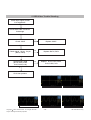
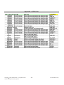
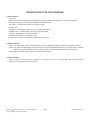
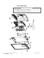
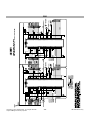
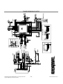
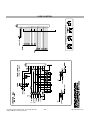
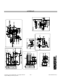
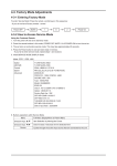
1
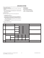
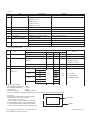
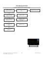
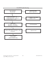
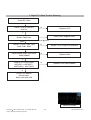
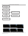
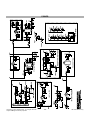
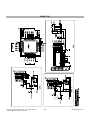
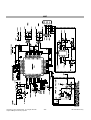
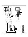
Internal Use Only
North/Latin America
Europe/Africa
Asia/Oceania
http://aic.lgservice.com
http://eic.lgservice.com
http://biz.lgservice.com
LCD MONITOR TV
SERVICE MANUAL
CHASSIS : LD84J
MODEL : M237WD
M237WD-PMJ
CAUTION
BEFORE SERVICING THE CHASSIS,
READ THE SAFETY PRECAUTIONS IN THIS MANUAL.
CONTENTS
CONTENTS .............................................................................................. 2
PRECAUTIONS .........................................................................................3
SPECIFICATION ........................................................................................6
ADJUSTMENT INSTRUCTION ...............................................................12
TROUBLE SHOOTING ............................................................................15
BLOCK DIAGRAM...................................................................................24
DESCRIPION OF BLOCK DIAGRAM .....................................................25
EXPLODED VIEW .................................................................................. 26
SVC. SHEET ...............................................................................................
Copyright C 2009 LG Electronics. Inc. All right reserved.
Only for training and service purposes
-2-
LGE Internal Use Only
SAFETY PRECAUTIONS
IMPORTANT SAFETY NOTICE
Many electrical and mechanical parts in this chassis have special safety-related characteristics. These parts are identified by
in the
Schematic Diagram and Exploded View.
It is essential that these special safety parts should be replaced with the same components as recommended in this manual to prevent
Shock, Fire, or other Hazards.
Do not modify the original design without permission of manufacturer.
Leakage Current Hot Check (See below Figure)
Plug the AC cord directly into the AC outlet.
General Guidance
An isolation Transformer should always be used during the
servicing of a receiver whose chassis is not isolated from the AC
power line. Use a transformer of adequate power rating as this
protects the technician from accidents resulting in personal injury
from electrical shocks.
It will also protect the receiver and it's components from being
damaged by accidental shorts of the circuitry that may be
inadvertently introduced during the service operation.
If any fuse (or Fusible Resistor) in this TV receiver is blown,
replace it with the specified.
When replacing a high wattage resistor (Oxide Metal Film Resistor,
over 1W), keep the resistor 10mm away from PCB.
Do not use a line Isolation Transformer during this check.
Connect 1.5K/10watt resistor in parallel with a 0.15uF capacitor
between a known good earth ground (Water Pipe, Conduit, etc.)
and the exposed metallic parts.
Measure the AC voltage across the resistor using AC voltmeter
with 1000 ohms/volt or more sensitivity.
Reverse plug the AC cord into the AC outlet and repeat AC voltage
measurements for each exposed metallic part. Any voltage
measured must not exceed 0.75 volt RMS which is corresponds to
0.5mA.
In case any measurement is out of the limits specified, there is
possibility of shock hazard and the set must be checked and
repaired before it is returned to the customer.
Leakage Current Hot Check circuit
Keep wires away from high voltage or high temperature parts.
AC Volt-meter
Before returning the receiver to the customer,
always perform an AC leakage current check on the exposed
metallic parts of the cabinet, such as antennas, terminals, etc., to
be sure the set is safe to operate without damage of electrical
shock.
Leakage Current Cold Check(Antenna Cold Check)
With the instrument AC plug removed from AC source, connect an
electrical jumper across the two AC plug prongs. Place the AC
switch in the on position, connect one lead of ohm-meter to the AC
plug prongs tied together and touch other ohm-meter lead in turn to
each exposed metallic parts such as antenna terminals, phone
jacks, etc.
If the exposed metallic part has a return path to the chassis, the
measured resistance should be between 1MΩ and 5.2MΩ.
When the exposed metal has no return path to the chassis the
reading must be infinite.
An other abnormality exists that must be corrected before the
receiver is returned to the customer.
Copyright C 2009 LG Electronics. Inc. All right reserved.
Only for training and service purposes
-3-
To Instrument’s
exposed
METALLIC PARTS
Good Earth Ground
such as WATER PIPE,
CONDUIT etc.
0.15uF
1.5 Kohm/10W
When 25A is impressed between Earth and 2nd Ground
for 1 second, Resistance must be less than 0.1 Ω
*Base on Adjustment standard
LGE Internal Use Only
SERVICING PRECAUTIONS
CAUTION: Before servicing receivers covered by this service
manual and its supplements and addenda, read and follow the
SAFETY PRECAUTIONS on page 3 of this publication.
NOTE: If unforeseen circumstances create conflict between the
following servicing precautions and any of the safety precautions on
page 3 of this publication, always follow the safety precautions.
Remember: Safety First.
General Servicing Precautions
1. Always unplug the receiver AC power cord from the AC power
source before;
a. Removing or reinstalling any component, circuit board
module or any other receiver assembly.
b. Disconnecting or reconnecting any receiver electrical plug or
other electrical connection.
c. Connecting a test substitute in parallel with an electrolytic
capacitor in the receiver.
CAUTION: A wrong part substitution or incorrect polarity
installation of electrolytic capacitors may result in an
explosion hazard.
2. Test high voltage only by measuring it with an appropriate high
voltage meter or other voltage measuring device (DVM,
FETVOM, etc) equipped with a suitable high voltage probe.
Do not test high voltage by "drawing an arc".
3. Do not spray chemicals on or near this receiver or any of its
assemblies.
4. Unless specified otherwise in this service manual, clean
electrical contacts only by applying the following mixture to the
contacts with a pipe cleaner, cotton-tipped stick or comparable
non-abrasive applicator; 10% (by volume) Acetone and 90% (by
volume) isopropyl alcohol (90%-99% strength)
CAUTION: This is a flammable mixture.
Unless specified otherwise in this service manual, lubrication of
contacts in not required.
5. Do not defeat any plug/socket B+ voltage interlocks with which
receivers covered by this service manual might be equipped.
6. Do not apply AC power to this instrument and/or any of its
electrical assemblies unless all solid-state device heat sinks are
correctly installed.
7. Always connect the test receiver ground lead to the receiver
chassis ground before connecting the test receiver positive
lead.
Always remove the test receiver ground lead last.
8. Use with this receiver only the test fixtures specified in this
service manual.
CAUTION: Do not connect the test fixture ground strap to any
heat sink in this receiver.
Electrostatically Sensitive (ES) Devices
Some semiconductor (solid-state) devices can be damaged easily
by static electricity. Such components commonly are called
Electrostatically Sensitive (ES) Devices. Examples of typical ES
devices are integrated circuits and some field-effect transistors and
semiconductor "chip" components. The following techniques
should be used to help reduce the incidence of component
damage caused by static by static electricity.
1. Immediately before handling any semiconductor component or
semiconductor-equipped assembly, drain off any electrostatic
charge on your body by touching a known earth ground.
Alternatively, obtain and wear a commercially available
discharging wrist strap device, which should be removed to
prevent potential shock reasons prior to applying power to the
Copyright C 2009 LG Electronics. Inc. All right reserved.
Only for training and service purposes
unit under test.
2. After removing an electrical assembly equipped with ES
devices, place the assembly on a conductive surface such as
aluminum foil, to prevent electrostatic charge buildup or
exposure of the assembly.
3. Use only a grounded-tip soldering iron to solder or unsolder ES
devices.
4. Use only an anti-static type solder removal device. Some solder
removal devices not classified as "anti-static" can generate
electrical charges sufficient to damage ES devices.
5. Do not use freon-propelled chemicals. These can generate
electrical charges sufficient to damage ES devices.
6. Do not remove a replacement ES device from its protective
package until immediately before you are ready to install it.
(Most replacement ES devices are packaged with leads
electrically shorted together by conductive foam, aluminum foil
or comparable conductive material).
7. Immediately before removing the protective material from the
leads of a replacement ES device, touch the protective material
to the chassis or circuit assembly into which the device will be
installed.
CAUTION: Be sure no power is applied to the chassis or circuit,
and observe all other safety precautions.
8. Minimize bodily motions when handling unpackaged
replacement ES devices. (Otherwise harmless motion such as
the brushing together of your clothes fabric or the lifting of your
foot from a carpeted floor can generate static electricity
sufficient to damage an ES device.)
General Soldering Guidelines
1. Use a grounded-tip, low-wattage soldering iron and appropriate
tip size and shape that will maintain tip temperature within the
range or 500ºF to 600ºF.
2. Use an appropriate gauge of RMA resin-core solder composed
of 60 parts tin/40 parts lead.
3. Keep the soldering iron tip clean and well tinned.
4. Thoroughly clean the surfaces to be soldered. Use a mall wirebristle (0.5 inch, or 1.25cm) brush with a metal handle.
Do not use freon-propelled spray-on cleaners.
5. Use the following unsoldering technique
a. Allow the soldering iron tip to reach normal temperature.
(500ºF to 600ºF)
b. Heat the component lead until the solder melts.
c. Quickly draw the melted solder with an anti-static, suctiontype solder removal device or with solder braid.
CAUTION: Work quickly to avoid overheating the circuit
board printed foil.
6. Use the following soldering technique.
a. Allow the soldering iron tip to reach a normal temperature
(500ºF to 600ºF)
b. First, hold the soldering iron tip and solder the strand against
the component lead until the solder melts.
c. Quickly move the soldering iron tip to the junction of the
component lead and the printed circuit foil, and hold it there
only until the solder flows onto and around both the
component lead and the foil.
CAUTION: Work quickly to avoid overheating the circuit
board printed foil.
d. Closely inspect the solder area and remove any excess or
splashed solder with a small wire-bristle brush.
-4-
LGE Internal Use Only
IC Remove/Replacement
Some chassis circuit boards have slotted holes (oblong) through
which the IC leads are inserted and then bent flat against the
circuit foil. When holes are the slotted type, the following technique
should be used to remove and replace the IC. When working with
boards using the familiar round hole, use the standard technique
as outlined in paragraphs 5 and 6 above.
Removal
1. Desolder and straighten each IC lead in one operation by gently
prying up on the lead with the soldering iron tip as the solder
melts.
2. Draw away the melted solder with an anti-static suction-type
solder removal device (or with solder braid) before removing the
IC.
Replacement
1. Carefully insert the replacement IC in the circuit board.
2. Carefully bend each IC lead against the circuit foil pad and
solder it.
3. Clean the soldered areas with a small wire-bristle brush.
(It is not necessary to reapply acrylic coating to the areas).
"Small-Signal" Discrete Transistor
Removal/Replacement
1. Remove the defective transistor by clipping its leads as close as
possible to the component body.
2. Bend into a "U" shape the end of each of three leads remaining
on the circuit board.
3. Bend into a "U" shape the replacement transistor leads.
4. Connect the replacement transistor leads to the corresponding
leads extending from the circuit board and crimp the "U" with
long nose pliers to insure metal to metal contact then solder
each connection.
Power Output, Transistor Device
Removal/Replacement
1. Heat and remove all solder from around the transistor leads.
2. Remove the heat sink mounting screw (if so equipped).
3. Carefully remove the transistor from the heat sink of the circuit
board.
4. Insert new transistor in the circuit board.
5. Solder each transistor lead, and clip off excess lead.
6. Replace heat sink.
Circuit Board Foil Repair
Excessive heat applied to the copper foil of any printed circuit
board will weaken the adhesive that bonds the foil to the circuit
board causing the foil to separate from or "lift-off" the board. The
following guidelines and procedures should be followed whenever
this condition is encountered.
At IC Connections
To repair a defective copper pattern at IC connections use the
following procedure to install a jumper wire on the copper pattern
side of the circuit board. (Use this technique only on IC
connections).
1. Carefully remove the damaged copper pattern with a sharp
knife. (Remove only as much copper as absolutely necessary).
2. carefully scratch away the solder resist and acrylic coating (if
used) from the end of the remaining copper pattern.
3. Bend a small "U" in one end of a small gauge jumper wire and
carefully crimp it around the IC pin. Solder the IC connection.
4. Route the jumper wire along the path of the out-away copper
pattern and let it overlap the previously scraped end of the good
copper pattern. Solder the overlapped area and clip off any
excess jumper wire.
At Other Connections
Use the following technique to repair the defective copper pattern
at connections other than IC Pins. This technique involves the
installation of a jumper wire on the component side of the circuit
board.
1. Remove the defective copper pattern with a sharp knife.
Remove at least 1/4 inch of copper, to ensure that a hazardous
condition will not exist if the jumper wire opens.
2. Trace along the copper pattern from both sides of the pattern
break and locate the nearest component that is directly
connected to the affected copper pattern.
3. Connect insulated 20-gauge jumper wire from the lead of the
nearest component on one side of the pattern break to the lead
of the nearest component on the other side.
Carefully crimp and solder the connections.
CAUTION: Be sure the insulated jumper wire is dressed so the
it does not touch components or sharp edges.
Diode Removal/Replacement
1. Remove defective diode by clipping its leads as close as
possible to diode body.
2. Bend the two remaining leads perpendicular y to the circuit
board.
3. Observing diode polarity, wrap each lead of the new diode
around the corresponding lead on the circuit board.
4. Securely crimp each connection and solder it.
5. Inspect (on the circuit board copper side) the solder joints of
the two "original" leads. If they are not shiny, reheat them and if
necessary, apply additional solder.
Fuse and Conventional Resistor
Removal/Replacement
1. Clip each fuse or resistor lead at top of the circuit board hollow
stake.
2. Securely crimp the leads of replacement component around
notch at stake top.
3. Solder the connections.
CAUTION: Maintain original spacing between the replaced
component and adjacent components and the circuit board to
prevent excessive component temperatures.
Copyright C 2009 LG Electronics. Inc. All right reserved.
Only for training and service purposes
-5-
LGE Internal Use Only
SPECIFICATION
NOTE : Specifications and others are subject to change without notice for improvement.
1. Application Range.
3.Test method
1) This spec sheet is applied all of the LCD TV with LD84J
chassis.
2) Not included spec and each product spec in this spec sheet
apply correspondingly to the following each country standard
and requirement of Buyer
3.1 Performance :
LGE TV test method followed
3.2 Demanded other specification
- Safety : UL,CSA,IEC specification
- EMC : FCC,ICES,IEC specification
2. Specification
Each part is tested as below without special appointment
1. Temperature : 20±5°C
2. Relative Humidity : 65±10%
3. Power Voltage : Standard input voltage (100~240V@50/60Hz)
*Standard Voltage of each product is marked by models
2.4 Specification and performance of each parts are followed
each drawing and specification by part number in
accordance with BOM.
2.5 The receiver must be operated for about 20 minutes prior
to the adjustment.
4. General Specification
4.1 PC
No
Item
Specification
1
Supported Sync. Type
Separate Sync., Digital
2
Operating Frequency
Analog
Horizontal
30 ~ 83kHz
Vertical
56 ~ 75 Hz
Horizontal
30 ~ 83kHz
Vertical
56 ~ 75 Hz
Analog
Max.
1920x1080 @ 60Hz
Recommand
1920x1080 @ 60Hz
Digital
Max.
1920x1080 @ 60Hz
Digital
3
Resolution
Remarks
Recommand
Cold Start : 50 A
1920x1080 @ 60Hz
4
Inrush Current
5
Operating Condition
Sync (H/V)
Video
LED
Wattage
Power S/W On
On mode
On/On
Active
Blue
55W (Max)
On/On
Active
Blue
45W (Typ)
Sleep mode
Off/On
On/Off
Power S/W Off
Off mode
-
Hot : 120 A
Off
Amber
1W
Off
Off
1W
6
MTBF
50,000 HRS with 90% Confidence level
7
Using Altitude
5,000 m (for Reliability) 3,000m(for FOS)
Copyright C 2009 LG Electronics. Inc. All right reserved.
Only for training and service purposes
-6-
Lamp Life 40,000 Hours (Min)
LGE Internal Use Only
4.2 TV
No
Item
Specification
1.
Receiving System
ATSC/64 &256 QAM/NTSC-M
2.
Available Channel
1)VHF :02~13
Remarks
USA ONLY
2)UHF :14~69
3)DTV :02-69
4)CATV :01~135
5)CADTV :01~135
3.
Input Voltage
1)AC 100 ~ 240V 50/60Hz
4.
Market
North America
5.
Screen Size
23 inch Wide(23.00 inch)
6.
Aspect Ratio
16:9
7.
LCD Module
LM230WF1-TLA1(1920 x1080)
8.
Operating Environment
1)Temp :0 ~40 deg
Non-Glare,Wide,LPL TN
2)Humidity :~80 %
9.
Storage Environment
1)Temp :-20 ~60 deg
2)Humidity :0 ~90 %
5. Optical characteristic specification
5.1 Chroma &Brightness.
No.
1.
2.
Specification
Item
Viewing Angle<CR>10>
Luminance
Remark
Min
typ
Right/Left
70/70
85/85
Up/Down
60/70
75/85
25 0
300
Luminance
Max
DVI or RGB
(cd/m2)
- Stnadard, 6500K
- Full White (100IRE)
Variance(%)
3.
Contrast Ratio
4.
Color Coordinates
75
CR
600
White
[CIE 1931]
1000
Wx
Wy
0.329
RED
Rx
Green
Gy
0.614
Bx
0.146
Blue
Full White/ Full black
0.313
Typ
0.644
Typ
Ry
0.336
-0.03
Gx
0.295
DVI or RGB
- Stnadard, 6500K
- Full White (100IRE)
By
0.072
* Optical Test Condition
- Surrounding Brightness Level : dark
- Surrounding Temperature
: 25 ± 5°C
- warm-up Time
: 30 Min
- Contrast, Brightness
: Outgoing condition
- *Incase of Vivid Mode, high level saturation may be occurred.Check gray linearity at standard mode.
* Active area
- Active area of LCD PANEL is in bezel of cabinet.
- Interval between active area and bezel
| A-B|<1.0 mm , | C-D|<1.0 mm
A: Interval between left of active area and bezel
B: Interval between right of active area and bezel
C: Interval between top of active area and bezel
D: Interval between bottom of active area and bezel
Copyright C 2009 LG Electronics. Inc. All right reserved.
Only for training and service purposes
C
Active Area
B
A
D
-7-
Bezel
LGE Internal Use Only
5.2 Chroma (PSM :PC Mode-Standard, AV Mode-Vivid)
** The W/B Tolerance is ±0.002 for Adjustment, but for DQA ±0.015
No
1.
2.
3.
4.
5.
Item
Min
Typ
Max
Remark
Cool
Wx
0.283
0.285
0.287
AV Mode
(9300K)
Wy
0.291
0.293
0.295
- RF/ AV1,2,3/ Component/ HDMI
Medium
Wx
0.293
0.295
0.297
- Vivid
(8000K)
Wy
0.203
0.305
0.307
- Cool/ Medium/ Warm: 85IRE
Warm
Wx
0.311
0.313
0.315
(6500K)
Wy
0.327
0.329
0.331
6500k
Wx
0.283
0.313
0.343
PC Mode
Wy
0.299
0.329
0.359
- RGB/ DVI
Wx
0.253
0.283
0.313
- Stnadard
Wy
0.268
0.298
0.328
- 6500K/ 9300K :Full White 100IRE
9300k
*The spec range of Color coordinates is same with the one of module,because this model does not adjust white balance.
6. SET Optical Feature
6.1 PC Mode (Measurement Condition:Full white/Standard/6500k)-> Measure the black luminance after 30 seconds.
No
1
Luminance(cd/m2)
Item
23 inch
Min
Typ
250
300
C/R
Max
Remark
Min
Typ
600:1
1000:1
DFC 30,000:1
6.2 AV Mode (Measurement Condition:Full white(100IRE)/Vivid)-> Measure the black luminance after 30 seconds.
No
Item
1
23 inch
Luminance(cd/m2)
Min
Typ
170
220
C/R(Min)
Max
Remark
RF,AV,COMPONENT,HDMI
400:1
6.3 Dynamic CR
- Dynamic CR Working Condition : Full Black Pattern( All Black, No pattern( MSPG Pattern# 2)) signal in D- sub & DVI
No
Item
Min
Typ
1
M237WD-PMJ
24000: 1
30000: 1
Max
Remark
For Checking Black Luminance, wait for over 1 minute.
7. Mechanical specification
No
1
Item
Content
Product
Width(W)
Dimension
Before Packing
560.8
After Packing
651
2
Product
Only SET
3
Cintaniner
Quantity
4
Stand Assy
193.2
427
mm
456
161
mm
Kg
7.4
Kg
20ft
Individual or
Palletizing
Type
Remark
Height(H)
5.6
With BOX
Loding
Unit
Length(L)
40ft
Indi.
Wooden
Indi.
Wooden
630
520
1260
1144
Detachable
Size (W x D x H) 271.2 x 193.2 x 108.4
5
Appearance
Tilt Degree
-5~15degree
Tilt force
0.8~3.5kgf
General
Refer to Standard of LG(56)G1-1020
Copyright C 2009 LG Electronics. Inc. All right reserved.
Only for training and service purposes
-8-
LGE Internal Use Only
8. Component Video Input (Y, PB, PR)
No.
Specification
Resolution
H-freq(kHz)
V-freq(Hz)
Remark
1.
720* 480
15.73
59.94
SDTV ,DVD 480I
2.
720* 480
15.73
60.00
SDTV ,DVD 480I
3.
720* 480
31.47
59.94
SDTV 480P
4.
720* 480
31.50
60.00
SDTV 480P
5.
1280* 720
44.96
59.94
HDTV 720P
6.
1280* 720
45.00
60.00
HDTV 720P
7.
1920* 1080
33.72
59.94
HDTV 1080I
8.
1920* 1080
33.75
60.00
HDTV 1080I
9.
1920* 1080
23.0
24.0
HDTV 1080P
10.
1920* 1080
33.75
30
HDTV 1080P
11.
1920* 1080
67.43
59.94
HDTV 1080P
12.
1920* 1080
67.5
60
HDTV 1080P
10. RGB/DVI
10.1 Input ( PC )
No.
Resolution
H-freq(kHz)
V-freq(Hz)
Pixel clock(MHz)
1
720*400
31.468
70.08
28.321
2
640*480
31.469
59.94
25.175
Remark
Input 848x480 60Hz, 852x480 60Hz
-> 640x480 60Hz Display
3
640*480
37.5
75
31.5
4
800*600
37.879
60.317
40.0
5
800*600
46.875
75.0
49.5
6
1024*768
48.363
60.0
65.0
7
1024*768
60.123
75.029
78.75
8
1152* 864
67.500
75.000
108.0
9
1280* 1024
63.981
60.02
108.0
10
1280* 1024
79.976
75.035
135.0
11
1680* 1050
64.674
59.883
119.0
12
1680* 1050
65.290
59.954 1
46.25
13
1600* 1200
75.0
60.0
162.0
14
1920* 1080
66.587
59.934
138.5
10.3 RGB EDID Data
- Analog EDID_Product ID :22251
Copyright C 2009 LG Electronics. Inc. All right reserved.
Only for training and service purposes
-9-
LGE Internal Use Only
- DVI(Digital)EDID_Product ID :22252
- Adjustable Data :
*: Serial No. .( Input the S/ N at Total Assembly line)
**: week
***: year ex) when year 2006 : input “10”
**** : CHECK SUM (deferent along Serial No, week, year)
12. HDMI1,2
12.1 Input ( DTV: For Video, PC is not Supported)
No.
Resolution
H-freq(kHz)
V-freq(Hz)
Pixel clock(MHz)
Remark
1
720* 480
31.469 / 31.5
59.94 / 60
23.00/ 23.03
SDTV 480P
2
720* 576
31.25
50
54
SDTV 576P
3
1280* 720
37.500
50
74.25
HDTV 720P
4
1280* 720
44.96 / 45
59.94 / 60
74.17/ 74.25
HDTV 720P
5
1920* 1080
33.72 / 33.75
59.94 / 60
74.17/ 74.25
HDTV 1080I
6
1920* 1080
28.125
50.00
74.25
HDTV 1080I
7
1920* 1080
26.97 / 23
23.97 / 24
74.17/ 74.25
HDTV 1080P
8
1920* 1080
33.716 / 33.75
29.976 / 30.00
74.25
HDTV 1080P
9
1920* 1080
56.250
50
148.5
HDTV 1080P
10
1920* 1080
67.43 / 67.5
59.94 / 60
148.35/ 148.50
HDTV 1080P
Copyright C 2009 LG Electronics. Inc. All right reserved.
Only for training and service purposes
- 10 -
LGE Internal Use Only
11.2 EDID Data
- HDMI EDID - Product ID : 22253 ( HDMI1 and HDMI2 have the Same EDID)
1) HDMI1
2) HDMI2
1) All data are HEXA
2) Adjustable Data :
*: Serial No.
**: week
***: year ex) when year 2008 : input “12”
**** : CHECK SUM (deferent along Serial No, week, year)
Copyright C 2009 LG Electronics. Inc. All right reserved.
Only for training and service purposes
- 11 -
LGE Internal Use Only
ADJUSTMENT INSTRUCTION
5. Click "Auto" tab and set as below
6. Click "Run".
7. After downloading, check "OK" message.
1. Application
1) This spec sheet is applied all of the LCD TV with LD84J
chassis.
2)Not included spec and each product spec in this spec sheet
apply correspondingly to the following each country standard
and requirement of Buyer
(6)
filexxx.bin
(7)
.OK
2. Designation
1) The adjustment is according to the order which is designated
and which must be followed, according to the plan which can
be changed only on agreeing.
2) Power Adjustment: Free Voltage
3) Magnetic Field Condition: Nil.
4) Input signal Unit: Product Specification Standard
5) Reserve after operation: Above 30 Minutes
6) Adjustment equipments: Color Analyzer( CA- 210 or CA110), Pattern Generator ( MSPG- 925L or Equivalent ), DDC
Adjustment Jig equipment, SVC remote controller
(5)
3.1 ADC Process
3. Main PCB check process
# APC - After Manual-Insult, executing APC
# Download
1. Execute ISP program "Mstar ISP Utility" and then click
"Config" tab.
2. Set as below, and then click "Auto Detect" and check "OK"
message.
If display "Error", Check connect computer, jig, and set.
3. Click "Connect" tab.
If display "Can’t ", Check connect computer, jig, and set.
(1)
(2)
3.1.1 PC input ADC
3.1.1.1 Auto RGB Gain/Offset Adjustment
• Convert to PC in Input-source
I2C COMMAND: 0xF4(SELECT_INPUT)0x00 0x60 (RGB)
cf. 0x10(TV),0x20(AV),0x40(COMPONENT),0x60(RGB),
0x90(HDMI)
• Signal equipment displays
Output Voltage : 700 mVp-p
Impress Resolution XGA (1024 x 768 @ 60Hz)
Model: 60 in Pattern Generator
Pattern: 29 in Pattern Generator (MSPG-925 SERISE)
[gray pattern that left & right is black and center is white
signal (Refer below picture)].
(3)
OK
4. Click "Read" tab, and then load download file(XXXX.bin)
by clicking "Read"
(4)
filexxx.bin
Copyright C 2009 LG Electronics. Inc. All right reserved.
Only for training and service purposes
- 12 -
Adjustment pattern (PC )
• Adjust by commanding AUTO_COLOR_ADJUST(0xF1)
0x00 0x02 instruction.
3.1.1.2 Confirmation
• We confirm whether “0xB6(RGB)” address of EEPROM
“0xA2” is “0xAA”or not.
• If “0xB6(RGB)” address of EEPROM “0xB2” isn’t “0xAA”,
we adjust once more
• We can confirm the ADC values from “0xB0~ 0xB5(RGB)”
addresses in a page “0xA2”
*Manual ADC process using Service Remocon. After enter
Service Mode by pushing “INSTART” key, execute “AutoRGB” by pushing “ ” key at “Auto-RGB”.
LGE Internal Use Only
3.2.1COMPONENT input ADC
3.2.1.1Component Gain/Offset Adjustment
• Convert to Component in Input-source
I2C COMMAND :0xF4(SELECT_INPUT)0x00 0x40
(COMPONENT)
cf.0x10(TV),0x20(AV),0x40(COMPONENT),
0x60(RGB),0x90(HDMI)
• Signal equipment displays at SD Mode
Impress Resolution: 480i
MODEL :209in Pattern Generator(SD Mode)
PATTERN :08in Pattern Generator(MSPG-925
SERISE)
• Signal equipment displays at HD Mode
Impress Resolution:1080i
MODEL :223in Pattern Generator(HD Mode)
PATTERN :08in Pattern Generator(MSPG-925
SERISE)
4. Total Assembly line process
Adjustment pattern (COMPONENT )
• Adjust by commanding AUTO_COLOR_ADJUST(0xF1)
0x00 0x02 instruction
3.2.1.2 Confirmation
• We confirm whether “0xC8(1080i)”address of EEPROM
“0xA2” is “0xAA” or not.
• If “0xC8(1080i)” address of EEPROM “0xA2” isn’t
“0xAA”, we adjust once more
• We can confirm the ADC values from “0xC2~(1080i)”
addresses in a page “0xA2”
3.2 Function Check
3.2.1 Check display and sound
• Check Input and Signal items. ( cf. work instructions)
1.TV
2.AV (CVBS/ S-Video)
3.COMPONENT (1080i)
4.RGB (PC: 1680X1050 @60Hz)
5.HDMI
6.PC Audio In and H/P Out
* Display and Sound check is executed by Remote controller.
Copyright C 2009 LG Electronics. Inc. All right reserved.
Only for training and service purposes
- 13 -
4.1 Adjustment Preparation
• Above 30 minutes H/run in RF no signal
• 15 Pin D-Sub Connector, for IIIC communication not
including VGA signal,is connected to AUTO W/B
EQUIPMENT..
4.2 Check coordinate of 9300K
•Set Input mode to RGB.
• Set Temperature : 9300K
• Adjust x: 0.285±0.005, y: 0.293±0.005(9300°K )
(Full white MSPG series Pattern 4)
4.3 Check color coordinate of 6500K
• Set Input mode to RGB.
• Set Temperature : 6500K
• Adjust x:0.313±0.005, y:0.329±0.005(6500°K )
(Full white MSPG series Pattern 4)
4.4 DPM operation confirmation (Only Apply for MNT Model)
Check if Power LED Color and Power Consumption operate
as standard.
• Set Input to RGB and connect D-sub cable to set
• Measurement Condition : (100~240V@50/60Hz)
• Confirm DPM operation at the state of screen without
Signal
4.5 DDC EDID Write Model Name(M237WD-PMJ):
• Connect D- sub Signal Cable to D-Sub Jack.
• Connect DVI Signal Cable to DVI Jack.
• Connect HDMI1,2 Signal Cable to HDMI1,2 Jack.
• Write EDID DATA to EEPROM(24C02) by using DDC2B
protocol.
• Check whether written EDID data is correct or not.
(refer to Product spec).
4.6 HDCP (High-Bandwidth Digital Contents Protection)SETTING
• Connect D-sub Signal Cable to D-Sub Jack
• Input HDCP key with HDCP-key-in-program
• HDCP Key value is stored on EEPROM(AT24C512)
which is 80~A1 addresses of 0xA0~0xA2 page
• AC off/on and on HDCP button of MSPG925 and
confirm whether picture is displayed or not of using
MSPG925
• HDCP Key value is different among the sets.
4.7 Outgoing condition Configuration
• After all function test., press IN-STOP Key by SVC
Remote controller. And Make Ship Condition.
• When pressing IN-STOP key by SVC remocon, Red
LED are blinked alternatively. And then Automatically
turn off. (Must not AC power OFF during blinking)
4.8 Internal pressure
• Confirm whether is normal or not when between power
board's ac block and GND is impacked on 1.5kV(dc) or
2.2kV(dc) for one second
LGE Internal Use Only
5.3 E2PROM Data Write
5. Adjustment Command
5.3.1 Signal Table
5.1 Adjustment Commands(LEMGTH=84)
START
No.
Adjustment Contents
CMD ADR
VAL
Description
1
FACTORY ON
E0
00
00
Factory mode on
2
FACTORY OFF
E2
00
00
Factory mode off
3
EEPROM ALL INIT.
E4
00
00
EEPROM All c lear
4
EEPROM Read
E7
00
00
EEPROM Read
5
EEPROM Write
E8
00
Data
EEPROM Write by so me values
6
COLOR SAVE (R/G/B cutoff)
EB
Drive, Contrast, Bright)
00
00
Color Save
7
H POSITION
20
00
00~100
8
V POSITION
30
00
00~100
9
CLOCK
90
00
00~100
10
PHASE
92
00
00~100
11
R DRIVE
16
00
00~FF
12
G DRIVE
18
00
00~FF
They have different range
B DRIVE
1A
00
00~FF
80
00
00~7F
15
G CUTOFF
82
00
00~7F
16
B CUTOFF
84
00
00~7F
17
BRIGHT
10
00
00~3F
19
CONTRAST
12
00
00~64
20
AUTO_COLOR_ ADJU ST
F1
00
02
21
CHANGE_COLOR_TEMP
F2
00
0: COOL
0,1,2,3 1: NORMAL
2: WARM
3: USER
23
F4
AUTO_INPUTCHANGE
00
00
A
03
Data_n
A CMD A ADH A
A
CS
A
ADL A
STOP
CMD(hex)
LEN
Details
1
EEPROM WRITE
E8
94
16-Byte Write
84+n
n-byte Write
- use
• EDID write : 16-byte by 16-byte, 8 order (128-byte)
write(TO “00 – 7F” of “EEPROM Page A4”)
• FOS
Default
write
:
16-mode
data
(HFh,HFl,VF,STD,HP,VP,Clk,ClkPh,PhFine) write
• Random Data write : write the appointment Address of
E2PROM
Offset adjustment
Bright adjustment
Luminance adjustment
5.4 VRAM Read
• Send CMD(70h) to read Video RAM value from MICOM
And save its value to 128-Bytes Buffer(Common Buffer
for the use of EDID)
START 6E A
Factory mode off
& II_SW is 1
& Input change to TV
0,1,2,4
...
Adjustment contents
Auto COLOR Adjustment
00
A 84+n
No.
Drive adjustment
R CUTOFF
F3
50
A
2
14
FACTORY_DEFAULT
A
LEN : 84h + Byte
CMD : 8Eh
ADH : E2PROM Slave Address (A0, A2, A4, A8), Not 00h
(Reserved by Buffer to E2PROM )
ADL : E2PROM Sub Address ( 00~ FF)
Data : Write data
5.3.2 Command Set
mode, FOS Adjustment
13
22
6E
Data_1
50 A
84
A
03 A
70
A
00
A
00
A CS A
STOP
3 :
Component
• Delay 500ms ( Time to Wait and Read Video RAM from
MICOM)
• Be transmitted the contents of MICOM’s 128-bytes
Buffer to PC.
(128th Data is the CheckSum of 127-bytes data : That’s
OK if the value of adding 128-bytes Data is Zero)
4 :
RGB
START
5 :
DVI
6 :
HDMI
0 :
1 :
TV
AV1
2 :
AV2
6F A
Data1
...
Data128 A CS NA
STOP
5.2 EEPROM DATA READ
5.2.1 Signal Table
START
6E
A
50
A
84
CS
A
STOP
START
6F
A
D1
A
---------------------------------------------------------------------- Dn
A
STOP
A
03
A CMD A ADH
A
ADL
A
128 Bytes
5.2.2 Command Set
No.
1
Adjustment contents
EEPROM READ
CMD A DH
E7
A0
2
3
A2
8
0
80
A4
6
7
0
80
4
5
ADL
0
80
A6
0
80
Details
0-Page
0~7F Read
0-Page 80~FF Read
1-Page
0~7F Read
1-Page 80~FF Read
2-Page
0~7F Read
2-Page 80~FF Read
3-Page
0~7F Read
3-Page 80~FF Read
*use: To read the appointment Address of E
Copyright C 2009 LG Electronics. Inc. All right reserved.
Only for training and service purposes
- 14 -
LGE Internal Use Only
TROUBLESHOOTING
1. Power- Up Boot Fail Trouble Shooting
Check P700 All
Voltage Level (5V, 15V)
N
Check Pow er con nector
OK ?
N
Replace Po wer board
Y
Check Q702 Outp ut
Voltage Level (5V)
N
Replace Q702
Y
Check IC705 #2 Pin
Voltage Level 3.3V
N
Replace IC 705 &
Recheck
Y
Check X101 Clock
12MHz
N
Replace X 101
Y
Replace IC 106 Flash
Memory
Wave form of X101
Copyright C 2009 LG Electronics. Inc. All right reserved.
Only for training and service purposes
- 15 -
LGE Internal Use Only
2. No OSD Trouble Shooting
Check P70 0(#9)
INV_ON high
N
Check GPIO Path
(Refer to Appe ndix 1 .)
Y
1. Check Po wer Board , 15V
2. Check Q702 Output voltage(5V)
3. Check P302(#1, 2, 3) 5V
N
1. Replace Pow er Board
2. Replace Q702
Y
Check P30 2
#8(TXEC+) , #9(TXEC-) ,
#20(TXOC+) , #21(TXOC-)
N
IC101 has problem
Y
Check L VDS Cable for damage or ope n
con ductors .
Y
Replace Ca ble
N
Check L CD Module
Control board
(Refer to Module CAS)
Copyright C 2009 LG Electronics. Inc. All right reserved.
Only for training and service purposes
- 16 -
LGE Internal Use Only
3. Digital TV Video Trouble Shooting
Check RF Ca ble
Y
Check Tu ner 5V Po wer &
Q707 5V
N
Replace Q7 07
Y
Bad Tun er. Replace Tuner.
Check L D400 color
None
Check T P Clock, Data, Sync
R440, R441, R442
Yello w -> none
N
Maybe Tun er(TU400) has problems
Y
Check Demod ulator Input Clock
X400 (25MHz)
N
Replace X400
Y
Check IC10 1 LVDS output
#8(TXEC+) , #9(TXEC-) ,
#20(TXOC+) , #21(TXOC-)
N
Replace IC101 has problems
Y
Check L CD Module
Control board
Refer to Mo dule CAS
Wave form of X400
Copyright C 2009 LG Electronics. Inc. All right reserved.
Only for training and service purposes
- 17 -
LGE Internal Use Only
4. Component Video Trouble Shooting
Check inpu t signal for mat
Is it supported?
Y
Check Compo nent Cab le
Y
N
Replace JK602 or Che ck Divice
Check J K602
Y
Check signal
C124, C126, C129
N
Check R10 7, R109, R112,
C124, C126, C129
Y
IC101 has problem
Wave form of Comp Y
Wave form of Comp Pb
Wave form of C124
Copyright C 2009 LG Electronics. Inc. All right reserved.
Only for training and service purposes
Wave form of C126
- 18 -
Wave form of Comp Pr
Wave form of C129
LGE Internal Use Only
5. RGB Video Trouble Shooting
Check inpu t signal format
Is it supported?
Y
Check RGB Cable connector
for damage
Y
N
Replace JK607
Check JK607
Y
Check signal , Hsync, Vsync
(R673, R674)
N
Replace R6 73, R674
Y
Check signal RGB
(R119, R104, R105
C121,C122,C119)
N
Replace R119, R104, R105,
C121,C122,C119
Y
IC101 has problem
Wave form of R673(Vsync)
Wave form of R105/C122
Copyright C 2009 LG Electronics. Inc. All right reserved.
Only for training and service purposes
Wave form of R104/C121
- 19 -
Wave form of R673(Vsync)
Wave form of R119/C119
LGE Internal Use Only
6. AV Video Trouble Shooting
Check inpu t signal for mat
Is it supported?
Y
Check AV Ca ble / S-Video Cable f or
damage or ope n conn ector
Y
Check signal R611(AV_CVBS),
R625, R626(S_Video)
N
Replace R6 11, R625, R626
Y
Check signal RGB
R116, R113, R114
C137, C134, C135
N
Replace R1 16, R113, R114
C137, C134, C135
Y
IC101 has problem
Wave form of R611(CVBS)
Wave form of R625(S-video)
Copyright C 2009 LG Electronics. Inc. All right reserved.
Only for training and service purposes
- 20 -
Wave form of R626(S-video)
LGE Internal Use Only
7.HDMI Video Trouble Shooting
Check input signal form at
Is it supported?
Y
Check HD MI Cable for damage o r open
conn ecto r
Y
Check JK801 / JK802 for proper connectio n or
dam age
N
Replace c onn ector
Y
Check IC803 Out Volta ge Level
3.3V(Pin 6)
N
Replace IC803
Y
Check ED ID NVRAM
(IC801, IC802)
Power & I2 C Sig nal (#5, #6)
Y
N
Check HD CP Key NVRAM (IC105)
Power & I2 C Sig nal (#5, #6)
N
Redownloa d EDID data or
Rep ace IC801/IC802
l
Replace IC105
Y
Replace Ms tar (IC101)
Copyright C 2009 LG Electronics. Inc. All right reserved.
Only for training and service purposes
- 21 -
LGE Internal Use Only
8. All Source Audio Trouble Shooting
Make sure yo u can t hear any audi o
and Device sup port the au di o sig nal
norm ally .
Y
Check Speaker and it s w ire
con nectio n (P500)
An d the resistance
N
Replace co nnector or Speaker
Y
Check 15V From Po wer board
(P700, Pin #1,2)
An d Check Aud io Amp Pow er 12V
(IC501, Pin#2, 3, 3 4, 35, 40, 41, 44, 45)
N
Replace P ower Board or Check
L511
Y
Check Sig nal from IC501
L502, L503, L504, L505
N
Replace IC 500
Y
Check Sig nal from IC101
(R130, R131, R1021, R1022)
Copyright C 2009 LG Electronics. Inc. All right reserved.
Only for training and service purposes
N
- 22 -
Replace IC 101
LGE Internal Use Only
Appendix 1. GPIO Path.
Copyright C 2009 LG Electronics. Inc. All right reserved.
Only for training and service purposes
- 23 -
LGE Internal Use Only
Copyright C 2009 LG Electronics. Inc. All right reserved.
Only for training and service purposes
- 24 -
RS232C
RF
COMP
S-VIDEO
AV
SCART(Full)
PC_Audio
RGB
(PC Only)
DVI-D
(PC Only)
HDMI1, 2
(DTV Only)
MAX3232CDR
RX / TX
IC700
COMP_LR_IN
COMP_ YPbPr
S-VIDEO_DET
CVBS_LR_IN
S-VIDEO_YC_IN
CVBS_IN
TV_VOUT
TV_LR_OUT/
RXD / TXD
TV_MAIN/MAIN_SIF
IIC_TUNER
AMP
GAIN X 4
LGE6991DD
MSTAR
DDR
I2S
REG
3.3V
2.5V
MP2305
MP2305
DC-DC
DC-DC
REG
3.3V
TAS5709
Digital AMP
EARPHONE
AMP
TPA6110
15V
LCD
(LVDS)
MX25L1605
AM2C-15G
24C64
EEPROM
+5V
SWITCH
DUAL FET
PSU
SPK 2CH
5V_ST
SPI_D
PANEL_CTL/POWER_ON/OFF
+1.25V_ST
+5V_TUNER
INV_CTL/
DIMMING
SW_RESET / IIC_AMP
EAR_LR_OUT/MUTE
IIC_PART
SPI_CZ/CLK
HYB25DC256163CE-4
LVA[0:3] / LVB[0:3] / LVACLK/ LVBCLK
MDATA[0:15]
MADR[0:11]
TMDS/DDC/
HDMI_SEL/HDMI_IIC
HDMI
S/W
TMDS351PAG
RGB/HVS/IIC_DSUB
DDC
SC_VIN/ID1/FB/RGB
SCART_LRIN
PC_AUD
24C02BN
EEPROM
HDMI3_5V_DET(HPD)
HDMI 1,2 TMDS/DDC/HPD_S/W
DDC
24C02BN
24C02BN
EEPROM
24C02BN
EEPROM
EEPROM
PANEL_POWER
BLOCK DIAGRAM
LGE Internal Use Only
DESCRIPTION OF BLOCK DIAGRAM
1.Input Interface.
1-1.PC Input
- RGB Input is directly transmitted to LGE1854C(scaler,Clock 12Mhz) and display up to 1920*1080 resolution
- DVI Signal input go to scaler through TMSD351(DVI/HDMI Switch)
- PC Audio is connected PC-Audio input by Stereo Cable
1-2 Video Input
- Component :YPbPr/YCbCr signal input, Up to 1080P Resolution.
- CVBS/S-Video : CVBS/S-Video signal input, supporting 480P
- HDMI 1,2 :Digital signal input(Included Audio)
1-3 RF(ATSC/NTSC)Input :ATSC/NTSC Input.
1-4 Audio Input :Component L/R,Audio L/R,Stereo(For PC) input.
2.Output Interface
- Video :The video signal goes to LGE1854C(Scaler)-> Frame Memory(210MHz:converted LVDS signal)->Module
- Audio :The audio is divided Digital signal at Scaler go through NTP3000A(Audio Amp IC) and generate to Speaker
Head-phone signal is divided to stereo signal at Scaler, then generate Headphone Amp(IC TPA6110)
- Optical Output :Generate audio output from Scaler(SPDIF(Optical)
3.Power Interface
- Input 5V,15V from Power Board is converted to 3.3V,2.6V,1.8V,1.25V,1.2V by Regulator and DC/DC Converter
Supply power to Module,Audio Amp and IC
Copyright C 2009 LG Electronics. Inc. All right reserved.
Only for training and service purposes
- 25 -
LGE Internal Use Only
EXPLODED VIEW
IMPORTANT SAFETY NOTICE
300
510
520
500
200
120
810
530
540
910
800
900
400
Many electrical and mechanical parts in this chassis have special safety-related characteristics. These parts
are identified by
in the Schematic Diagram and EXPLODED VIEW.
It is essential that these special safety parts should be replaced with the same components as recommended
in this manual to prevent X-RADIATION, Shock, Fire, or other Hazards.
Do not modify the original design without permission of manufacturer.
Copyright
LG Electronics. Inc. All right reserved.
Only for training and service purposes
- 26 -
LGE Internal Use Only
SCHEMATIC DIAGRAM
MAIN
Copyright C 2008 LG Electronics. Inc. All right reserved.
Only for training and service purposes
- 27 -
LGE Internal Use Only
DDR
Copyright C 2008 LG Electronics. Inc. All right reserved.
Only for training and service purposes
- 28 -
LGE Internal Use Only
TUNER/ DEMODULELATOR
Copyright C 2008 LG Electronics. Inc. All right reserved.
Only for training and service purposes
- 29 -
LGE Internal Use Only
LVDS/ CONTROL
Copyright C 2008 LG Electronics. Inc. All right reserved.
Only for training and service purposes
- 30 -
LGE Internal Use Only
INTERFACE
Copyright C 2008 LG Electronics. Inc. All right reserved.
Only for training and service purposes
- 31 -
LGE Internal Use Only
POWER
Copyright C 2008 LG Electronics. Inc. All right reserved.
Only for training and service purposes
- 32 -
LGE Internal Use Only
HDMI / DVI
Copyright C 2008 LG Electronics. Inc. All right reserved.
Only for training and service purposes
- 33 -
LGE Internal Use Only
AMP
Copyright C 2008 LG Electronics. Inc. All right reserved.
Only for training and service purposes
- 34 -
LGE Internal Use Only
LED_IR_HP
Copyright C 2008 LG Electronics. Inc. All right reserved.
Only for training and service purposes
- 35 -
LGE Internal Use Only
CONTROL KEY
Copyright C 2008 LG Electronics. Inc. All right reserved.
Only for training and service purposes
- 36 -
LGE Internal Use Only
P/NO : MFL49414510
Jan., 2009
Printed in Korea