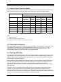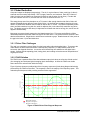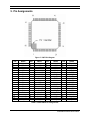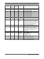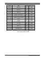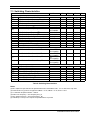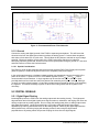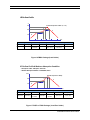
1
FS453/4 AND FS455/6 DATA SHEET: HARDWARE REFERENCE FS453/4 and FS455/6 PC-to-TV Video Scan Converter FS453/4 and FS455/6 Data Sheet Guides To make specialized information easier to find, the FS453/4 and FS455/6 Data Sheet is organized into separate reference guides. Each guide addresses a different purpose or user. The FS453/4 and FS455/6 Product Brief provides general information for all users. ; The FS453/4 and FS455/6 Hardware Reference is for system designers. It provides information on developing FS453/4 and FS455/6 applications. (This section now includes PCB Layout Guide) The FS453/4 and FS455/6 Software/Firmware Reference is for programmers. It provides information on programming the FS453/4 and FS455/6. If you need additional reference guides, contact your Focus Enhancements representative. Throughout this document "FS453" is used as a general term to reference the FS453, FS454, FS455, and FS456. The FS453 and FS454 are the PQFP versions of the chip, and the FS455 and FS456 are the BGA versions of the chip. The FS454 and FS456 support Macrovision anti-copy protection, while the FS453 and FS455 do not. JANUARY, 2005, VERSION 3.0 1 COPYRIGHT ©2003-4 FOCUS ENHANCEMENTS, INC. FOCUS Enhancements Semiconductor FS453/4 AND FS455/6 DATA SHEET: HARDWARE REFERENCE Table of Contents, Figures & Tables 9.1.1 Power ........................................ 30 9.1.2 Ground ...................................... 31 9.2 DIGITAL SIGNALS ............................. 31 9.2.1 Digital Signal Routing................ 31 9.2.2 Video Inputs .............................. 32 9.3 ANALOG SIGNALS ............................ 32 9.3.1 Video Output Filters .................. 32 9.4 CLOCK/OSCILLATOR........................ 34 9.4.1 Reference Crystal Oscillator ..... 34 9.4.2 FS453 Pixel Clock..................... 34 9.4.3 Pixel Clock Mode ...................... 35 9.5 EMI Case Study.................................. 37 9.6 Solder Re-flow Profiles ....................... 38 10. Revision History 40 11. Order Information 41 Document Overview 3 1. Introduction 4 1.1 General Description ..............................4 1.2 How does it work?.................................4 1.2.1 SDTV Output ...............................4 1.2.2 HDTV Output...............................4 1.2.3 VGA (RGB) Output......................4 1.3 General Physical Requirements ...........4 2. Architectural Overview 5 2.1 Inputs ....................................................5 2.1.1 Input to Output Conversion Matrix6 2.2 Color Space Converter .........................6 2.3 Patented 2D Scaler ...............................6 2.4 Patented 2D Flicker Filter .....................7 2.5 FIFO 7 2.6 Post (Horizontal Up) Scaler ..................7 2.7 Encoder and Inverse Color Space........7 2.8 Bi and Tri-Level Sync Insertion (HDTV) 7 2.9 Configurable 10 bit DACs .....................7 2.10 Clock Management ...............................7 2.11 Oscillators and PLL ...............................7 2.12 Serial Control Interface .........................8 2.13 Sync Timing Generator .........................8 2.14 Input Synchronization ...........................8 3. Technical Highlights 9 3.1 Scaling ..................................................9 3.1.1 Video Scaler Challenges.............9 3.1.2 FS453 Solution............................9 3.2 Flicker Reduction ................................10 3.2.1 Flicker Filter Challenges............10 3.2.2 FS453 Solution..........................10 3.3 Video Encoding ...................................11 3.3.1 Encoding Challenges ................11 3.3.2 FS453 Solution..........................11 4. Scaling and Positioning Notes 12 4.1 Vertical Scaling ...................................12 4.2 Horizontal Scaling ...............................13 4.3 Vertical and Horizontal Position ..........13 5. Pin Assignments 14 5.1 FS453 ⇔ GCC Pin Mapping...............16 5.2 Pin Descriptions ..................................17 6. Control Register Function Map 21 6.1 Register Reference Table ...................21 7. Specifications 24 7.1 Absolute Maximum and Recommended Ratings ................................................24 7.2 Electrical Characteristics.....................25 7.3 Switching Characteristics....................27 8. Mechanical Dimensions 28 8.1 80-Lead PQFP Package .....................28 8.2 88-Lead FBGA Package .....................29 9. Component Placement 30 9.1 Power/Ground .....................................30 JANUARY, 2005, VERSION 3.0 Figure 1: FS453 Functional Block Diagram..............5 Figure 2: FS453 Scaler Luma Frequency Response .........................................................9 Figure 3: FS453 Flicker Filter Diagonal Response .......................................................10 Figure 4: Equations for VTOTAL and VSC.............12 Figure 5: VTOTAL and VACTIVE ratios must match..............................................................12 Figure 6: HSC Equations ........................................13 Figure 7: PQFP Pin Diagram ..................................14 Figure 8 FBGA Pin Diagram ...................................15 Figure 9: PQFP Package Outline & Dimensions....28 Figure 10 FBGA Package Outline & Dimensions...29 Figure 11: Recommended Power Filter Networks ........................................................31 Figure 12: Recommended Output Filter .................33 Figure 13: Pixel Clock Pseudo-master Mode .........36 Figure 14: Pixel Clock Slave Mode.........................36 Figure 15 PQFP Package (Lead Solder)................38 Figure 16 FBGA Package (Lead Solder)................39 Figure 17 PQFP or FBGA Package (Lead-Free Solder)............................................................39 Table 1: Input to Output Conversion Matrix..............6 Table 2: FS453 PQFP Pin Assignments ................14 Table 3: FS453 to GCC Pin Mapping .....................16 Table 4: FS453 Pin Descriptions ............................20 Table 5: Register Reference Table.........................23 Table 6: Absolute Maximum and Recommended Ratings ...........................................................24 Table 7: Electrical Characteristics ..........................26 Table 8: Switching Characteristics .........................27 Table 9: Package Dimensions................................28 Table 10: Output Filter Component Values ............34 2 COPYRIGHT ©2003-4 FOCUS ENHANCEMENTS, INC. FOCUS Enhancements Semiconductor FS453/4 AND FS455/6 DATA SHEET: HARDWARE REFERENCE Document Overview The Hardware Reference provides information needed to integrate the FS453 Video Processor into system hardware. The reference is divided into eight sections: 1. Introduction – explains the purpose and general flow of the FS453. Begins on page 4. 2. Architectural Overview – defines the major sections of the FS453 and describes how they work together. Begins on page 5. 3. Technical Highlights – explains technical challenges faced by scan converters, and explains how the FS453 accomplishes Scaling, Flicker Filtering, and Video Encoding. Begins on page 9. 4. Scaling and Positioning Notes– provides more detailed information on how the FS453 performs Scaling and Positioning. Begins on page 12. 5. Pin Assignments – lists the pin names and maps their correspondence to sample host graphics controller chips. Describes pin functions. Begins on page 14. 6. Control Register Function Map – lists the Control Register functions and register numbers. If you need more information about the Control Registers, please request a copy of the FS453/4 and FS455/6 Software / Firmware Reference from your Focus Enhancements representative. The Control Register Function Map begins on page 21. 7. Specifications – provides information on the Absolute Maximum and Recommended Ratings, the Electrical Characteristics, and the Switching Characteristics. Begins on page 24. 8. Mechanical Dimensions – describes the FS453's 80-lead PQFP and 88-lead FBGA packages. Begins on page 28. 9. Component Placement – gives guidelines for the placement and layout of components associated with the FS453. Begins on page 30. JANUARY, 2005, VERSION 3.0 3 COPYRIGHT ©2003-4 FOCUS ENHANCEMENTS, INC. FOCUS Enhancements Semiconductor FS453/4 AND FS455/6 DATA SHEET: HARDWARE REFERENCE 1. Introduction 1.1 General Description The FS453 PC to TV Video Scan Converter provides broadcast-quality scan conversion for graphics cards, motherboard chip sets, video game consoles, consumer electronics and other PC-to-TV applications. Compatible with most graphics controller chips (GCC), the FS453 takes in high-resolution computer graphics input (VGA through SXGA) and produces SDTV (Standard Definition Television) or HDTV (High Definition Television) analog output. In SDTV mode the FS453 converts, scales, removes flicker, interlaces and encodes the data into NTSC or PAL formats. In HDTV mode, it performs color space conversions and then inserts the required syncs for output. The FS453's patented technology enables it to scale the converted image to fill the TV screen and display flicker-free graphics with sharply defined text. 1.2 How does it work? The FS453 provides a glueless digital interface to most GCCs. It accepts computer-generated digital graphics input in RGB or YCrCb format. The FS453 receives initialization and basic configuration information through its I2C*-compatible SIO port with simple register Read/Write commands. How the FS453 actually processes and converts the graphics information depends on the kind of video output selected. (Refer to Figure 1: FS453 Functional Block Diagram on page 5.) 1.2.1 SDTV Output For example, to create SDTV output the FS453 first changes RGB video to YCrCb. It uses patented technology to scale (in other words, to proportionately increase or decrease) the number of video lines and pixels per line to correspond to the specific SDTV standard. This allows the FS453 to precisely fill the user's television screen without adding artifacts such as blank areas, or distorting the graphics image. The FS453 uses more patented technology to adaptively remove the flicker effects common to SDTV while keeping fine detail (such as text) clear and sharp. The FS453 then encodes the processed image into broadcast quality, interlaced SDTV video and sends it out through the DACs. For European SCART output, the FS453 converts the image into RGB video and sends the R, G and B signals through separate DACs. 1.2.2 HDTV Output To convert high-resolution computer graphics to high resolution HDTV output the FS453 converts the digital video (whether RGB or YCrCb format) to YPrPb (analog component video). It adds Bi- and TriLevel Syncs as required by the selected standard and routes the analog HDTV video through the DACs. 1.2.3 VGA (RGB) Output The FS453 can also provide VGA output. In this mode, it allows the GCC's RGB images to pass unchanged directly through to the DACs. The HSync and VSync signals must be driven by the GCC. 1.3 General Physical Requirements Implementing the FS453 in your system will require very few components – just a 27 MHz clock and passive parts. The FS453 uses an 80-lead Quad Flat Pack (PQFP) or an 88-lead Fine-pitch Ball Grid Array (FBGA) package and requires power from +1.8V digital and +3.3V analog supplies. * 2 2 Note: I C is a registered trademark of Philips Corporation. The FS453 Serial I/O bus is similar but not identical to the Philips I C bus. JANUARY, 2005, VERSION 3.0 4 COPYRIGHT ©2003-4 FOCUS ENHANCEMENTS, INC. FOCUS Enhancements Semiconductor FS453/4 AND FS455/6 DATA SHEET: HARDWARE REFERENCE 2. Architectural Overview The FS453 has the following major sections: Color Space Conv. 2D Scaler 2D Flicker Filter Broadcast Quality Encoder HDTV Bi- & Tri-Level Sync Insertion Configurable 10 bit DACs Clock Management Oscillators and PLL Serial Control Interface Sync Timing Generator Inverse Color Space FIFO Post Scaler Encoder SDATA SCLK Crystal Clock Management XTAL OSC 10-bit DAC A 10-bit DAC B 10-bit DAC C 10-bit DAC D Bi & Tri-Level Sync Insertion Serial Control Interface ClkIn Multiplexer P[23:0] Multiplexer • • • • • • • • • • • Inputs P[23:0] Programmable Color Space Converter Patented 2D (Horizontal and Vertical) Scaling Patented 2D Flicker Filter FIFO Post (Horizontal Up) Scaler Inverse Color Space Demux • • • NCO to internal clocks Sync Timing Generator VSync HSync Blank Field ClkOut PLL Figure 1: FS453 Functional Block Diagram 2.1 Inputs The FS453 accepts computer graphics images in many different resolutions and pixel frequencies on P[23:0]. The FS453 adaptively process this information for optimal display on SDTV and HDTV television sets. JANUARY, 2005, VERSION 3.0 5 COPYRIGHT ©2003-4 FOCUS ENHANCEMENTS, INC. FOCUS Enhancements Semiconductor FS453/4 AND FS455/6 DATA SHEET: HARDWARE REFERENCE 2.1.1 Input to Output Conversion Matrix Table 1 below lists some commonly used input modes and the correspondingly supported output modes. SDTV input dimensions are completely configurable, subject only to pixel clock range limitations. Input Configuration Output Configuration SDTV Pixels Lines HDTV NTSC PAL 480p 720p 1080i @59.94Hz @50Hz @60Hz @60Hz @60Hz ∗(a) 640 - 720 480 ∗ ∗ 640 - 720 576 ∗ ∗ 800 600 ∗ ∗ 1024 768 ∗ ∗ 1280 720 ∗ (b) ∗ (b) 1920 1080 ∗(a) ∗(c) Table 1: Input to Output Conversion Matrix Notes: (a) No scaling supported (b) Subject to the maximum 150 MHz pixel rate (c) No scaling or interlacing supported, input data must be interlaced 2.2 Color Space Converter The programmable Color Space Converter receives either RGB or YCrCb data from the input port. If the data is RGB, it is converted to YCrCb using programmable coefficients. Each of the Y, Cr, and Cb components can then be independently scaled in amplitude with programmable multipliers. This programmability supports both SDTV and HDTV color space matrices. 2.3 Patented 2D Scaler The Patented 2D Scaler receives data from the Color Space Converter. It performs vertical (up or down) scaling based on the value programmed in the VSC (Vertical Scaling Coefficient) register, offset 06h. It performs horizontal (down) scaling based on the downscale value programmed in the HSC (Horizontal Scaling Coefficient) register, offset 08h. Because different video standards call for different numbers of lines and different numbers of pixels per line, scan converters add or subtract lines and areas to fit graphics images onto different sizes of TV screens. Most scan converters use simple line-dropping algorithms and fixed aspect ratios. Unfortunately, these techniques can introduce shape-distorting artifacts and surround the actual image with blank areas. The FS453, however, uses patented technology that can scale the graphics image without creating artifacts. The patented 2D Scaler can independently upscale or downscale an image in both the horizontal (pixels) and vertical (lines) directions. Its scaling functions provide equal weight to all pixels and lines in the source material for all scaling factors. This allows users to perfectly fit the graphics image to their TV screens without adding scaling artifacts or large blank borders. JANUARY, 2005, VERSION 3.0 6 COPYRIGHT ©2003-4 FOCUS ENHANCEMENTS, INC. FOCUS Enhancements Semiconductor FS453/4 AND FS455/6 DATA SHEET: HARDWARE REFERENCE 2.4 Patented 2D Flicker Filter The Patented 2D Flicker Filter receives video lines from the 2D Scaler and performs vertical filtering to reduce or eliminate perceived flicker that is an artifact of the interlaced television format. The FS453's flicker filter is significantly more effective than a typical three-line-average flicker filter. The FS453’s flicker filter consists of joint horizontal (Sharpness) and vertical (Flicker) controls. Three-lineaverage flicker filters do reduce the visual effect of interlaced image flicker, but they also introduce blurring. The flicker dimension of the FS453's filter reduces image flicker, while the sharpness dimension of the FS453's filter reduces image blurring. Both the sharpness and flicker registers can be programmed over a wide range of values to allow the user to customer tailor the filter settings to different display devices. 2.5 FIFO The Flicker Filter stores video data in a FIFO memory. This memory allows the video data to be transferred from the graphics clock domain to the TV clock domain. 2.6 Post (Horizontal Up) Scaler The Post Scaler draws information from the FIFO as necessary and scales it horizontally based on the up-scale value programmed in the Horizontal Scaling Coefficient (HSC) register. The scaled data is provided at the television clock rate to the SDTV video encoder and the Inverse Color Space. 2.7 Encoder and Inverse Color Space The FS453 contains a broadcast quality, 2X oversampled video encoder with an Inverse Color Space matrix. The encoder combines the chrominance, luminance, and timing information into broadcast quality NTSC or PAL composite and YC (S-Video) signals and sends them to the DACs. The Inverse Color Space transforms YCrCb video data to the RGB color space required for SCART output. If the Inverse Color Space is not used, then the Encoder converts YCrCb to YPrPb as required for SDTV YPrPb output. The RGB or YPrPb signals are sent to the DACs synchronized with the Encoder's composite signal. The FS454 and FS456, which are otherwise identical to the FS453 and FS455, respectively, incorporate Macrovision 7 anti-copy protection in the encoder. The FS454 and FS456 also include 480p protection. 2.8 Bi and Tri-Level Sync Insertion (HDTV) The FS453 also offers HDTV Syncs output modes. The color matrix, output level, and sync type are fully programmable allowing for compatibility with the multiple HDTV standards. The FS453 inserts bi-level or tri-level sync signals as defined by the standards. 2.9 Configurable 10 bit DACs The four output DACs (Digital/Analog Converters) can be configured for several output formats: RGB component output (VGA); RGB with CVBS (SCART); CVBS (2 optional) and Y/C (S-Video); and YPrPb component output (HDTV or SDTV). To conserve power the DACs can be run in low power mode or can be completely powered down when not in use. 2.10 Clock Management The FS453 synthesizes a 0.78125-150 MHz clock from the 27 MHz XTAL_IN and supplies this clock (CLKOUT) to the GCC. The clock is buffered and returned to the FS453 (CLKIN_P) synchronous to the pixel data and sync information. This clock has a 1.5 Hz resolution and can be adjusted so that the GCC scaled input data rate exactly matches the ITU-R BT.656 output data rate. 2.11 Oscillators and PLL The FS453 clock generation circuit operates in one of two modes, NCO (Numerically Controlled Oscillator) mode or PLL (Phase Locked Loop) mode. In NCO mode, the numerically controlled oscillator JANUARY, 2005, VERSION 3.0 7 COPYRIGHT ©2003-4 FOCUS ENHANCEMENTS, INC. FOCUS Enhancements Semiconductor FS453/4 AND FS455/6 DATA SHEET: HARDWARE REFERENCE is used to achieve the finest clock resolution, using a dithered clock. In PLL mode, the NCO is bypassed and the clock is not dithered. The NCO can be used when HTOTAL and VTOTAL values have additional constraints that prevent selection of values that are factors of the TV pixel rate. 2.12 Serial Control Interface The FS453 registers are accessed through a serial input/output bus (SIO) which is I2C*-compatible and SMBus-compatible. These registers can be read or written at any time the part is receiving a reference clock at XTAL_IN and not being held in reset via the RESET_L pin. 2.13 Sync Timing Generator The Sync Timing Generator provides/accepts HSync, VSync, Field and Blank signals to/from the graphics controller. 2.14 Input Synchronization The FS453 can operate in pseudo-master mode or slave mode. In pseudo-master mode, the GCC derives the VGA pixel clock, horizontal sync, and vertical sync from CLKOUT supplied by the FS453. In slave mode, the GCC generates the pixel clock, syncs and data, and the FS453 must be programmed to generate the same pixel clock, using a common reference. Use the slave mode when the GCC does not have a pixel clock input. * 2 2 Note: I C is a registered trademark of Philips Corporation. The FS453 Serial I/O bus is similar but not identical to the Philips I C bus. JANUARY, 2005, VERSION 3.0 8 COPYRIGHT ©2003-4 FOCUS ENHANCEMENTS, INC. FOCUS Enhancements Semiconductor FS453/4 AND FS455/6 DATA SHEET: HARDWARE REFERENCE 3. Technical Highlights Creating clear, broadcast quality television video from high resolution computer graphics is a complex process. PC-to-TV Video Scan Converters have to surmount many technical obstacles. The most challenging of these are scaling, flicker reduction, and encoding. 3.1 Scaling Converting high-resolution computer images into relatively low-resolution TV images (such as converting VGA or XGA images into NTSC standard definition television) is an inherently lossy process that requires a video scaler. For example, converting an image with 1000 pixels in a line into an image with only 500 pixels in a line, means that there must be 50% less data in each line of output. The video scaler has to perform its tasks effectively without further degrading the image. 3.1.1 Video Scaler Challenges Therefore, in addition to reducing pixel count and interpolating pixel values, the scaler must not alter the digital video data by adding artifacts. Examples of artifacts are the introduction of repeated pixels; the complete loss of pixel data; and the creation of new pixel colors that are not interpolations of original pixel colors. In effect, the video scaler should behave like a high quality filter. It should have a gradual frequency roll off with a good step response and little overshoot or ringing (less than 5%). This is ideal for maintaining video quality with detailed images (such as text). Detailed images produce rapid output step transitions that need to be executed cleanly. 3.1.2 FS453 Solution The following diagram (Figure 2) illustrates the response of the FS453's video scaler. It is a normalized plot of the Luma frequency response of the FS453's video scaler. As we can see, the FS453's patented video scaler behaves like a high quality filter with only a gradual frequency roll off. 5 Gain in Decibels 0 5 10 15 20 25 0 0.1 0.2 0.3 0.4 0.5 0.6 0.7 0.8 0.9 1 Normalized Frequency Scale 7/8 Scale 3/4 Scale 5/8 Scale 1/2 Figure 2: FS453 Scaler Luma Frequency Response JANUARY, 2005, VERSION 3.0 9 COPYRIGHT ©2003-4 FOCUS ENHANCEMENTS, INC. FOCUS Enhancements Semiconductor FS453/4 AND FS455/6 DATA SHEET: HARDWARE REFERENCE 3.2 Flicker Reduction Computer images are displayed progressively. That is, for a given frame of video, each line of video is scanned onto the monitor sequentially. SDTV images, however, are interlaced. Each SDTV frame of video is broken into two fields (one composed of odd lines and the other of even lines). First the odd lines are scanned onto the TV, and then the even lines are scanned onto the TV. The energy decay rate of the phosphors on a TV screen is fast enough that the older field of video will appear somewhat dimmer than the newer field of video. As the fields are constantly changing, this can result in a visible flicker between the two fields of data on the TV screen. This flicker is especially visible when one field contains a long dark line, while an adjacent line (in the other field) contains a long white line. The higher energy line will decay in brightness much faster than the low energy line, and in turn will appear to flicker heavily. Most scan converters simply average the pixel data between lines. This removes the Black-or-White relationships between lines that viewers recognize as video flicker. The problem with this solution is that data becomes blurred. Single black or white lines are reduced to grays. Detailed areas of video (such as the gap in the letter ‘e’) lose their distinction. 3.2.1 Flicker Filter Challenges The goal is to completely remove flicker from the image without blurring detailed video. To preserve the video details, the flicker filter should have a flat frequency response (+/- 1dB) between pixels in the horizontal, and diagonal directions. It must also avoid introducing new artifacts into the digital video stream. Artifacts include repeating pixels, losing pixels; and creating colors that are not interpolations of original pixel colors. 3.2.2 FS453 Solution The FS453 uses a patented flicker filter that calculates output pixel values as a function of both vertical (line averaging) and horizontal (pixel averaging) pixel relationships. In effect the FS453 can decide where and how to reduce flicker within the image. Figure 3 (below) shows a normalized plot of the frequency response of pixels along diagonal after being processed by the FS453's flicker filter. The response is flat for the majority of the frequency space. This maintains pixel sharpness while providing excellent flicker suppression. 1 0.75 Gain in Decibels 0.5 0.25 0 0.25 0.5 0.75 1 0 0.1 0.2 0.3 0.4 0.5 0.6 0.7 0.8 0.9 1 Normalized Frequency Horizontal Direction Diagonal at 27 degrees Diagonal at 45 degrees Figure 3: FS453 Flicker Filter Diagonal Response JANUARY, 2005, VERSION 3.0 10 COPYRIGHT ©2003-4 FOCUS ENHANCEMENTS, INC. FOCUS Enhancements Semiconductor FS453/4 AND FS455/6 DATA SHEET: HARDWARE REFERENCE 3.3 Video Encoding Unlike component video formats (PC and HDTV) that process the color information separately to avoid interference, broadcast SDTV combines all picture information into a single, composite signal. SDTV standards have been strictly defined to protect video quality and to allow television manufacturers to design and build large volumes of systems with confidence that their signal decoders will work— regardless of variances in final product tolerances. 3.3.1 Encoding Challenges If a video encoder does not adhere closely to these standards, it may produce video artifacts on many consumer televisions. Unfortunately, most scan converters use signal encoders that don't strictly follow NTSC and PAL guidelines. Their encoders can increase artifacts such as chroma crawl and color bleeding/smearing. To meet broadcast quality a video encoder must comply with the NTSC (EIA-170A, SMPTE-170M) and PAL (ITU-R624-3) standards in all modes. Of key importance are the specifications related to accurate timing and signal amplitudes, video subcarrier frequency good to +/- 5Hz, and horizontal lock with zero SC-H phase. The encoder must use a low jitter crystal (50 ppm) to drive DAC output directly. The DACs should have 10 bits of resolution, and exhibit good differential gain and differential phase characteristics. The video encoder must be able to pre-filter composite video (CVBS) to prevent luma(Y)/chroma(C) cross talk. 3.3.2 FS453 Solution The FS453 features a broadcast quality encoder. It uses tunable Y-notch and C-bandpass filters to prevent the creation of video artifacts and to meet all specifications. The FS453's encoder subcarrier is programmable in frequency and phase. Because of the encoder's independence of color format, vertical sync, and number of lines, the FS453 is able to support many SDTV video standards, including all of the South American variations. The FS453 can output NTSC M, J and PAL B, D, G, H, I, M, N, Combination N, and PAL-60 formats with 10 bits of resolution. Both Composite and S-Video outputs are available simultaneously. In addition to encoded PAL or NTSC, the user may select analog SCART RGB outputs. Each channel of RGB has 10 bits of resolution. Note that the 10-bit DACs exceed the bit depth supported by the 8-bits available at the FS453 input. JANUARY, 2005, VERSION 3.0 11 COPYRIGHT ©2003-4 FOCUS ENHANCEMENTS, INC. FOCUS Enhancements Semiconductor FS453/4 AND FS455/6 DATA SHEET: HARDWARE REFERENCE 4. Scaling and Positioning Notes The FS453 graphics converter does not use a frame memory. Therefore, the FS453 input video frame rate must be synchronous to and match the output video field or frame rate. In SDTV modes, the FS453 uses internal line memories in order to perform horizontal and vertical scaling. This imposes certain requirements on the scale and position settings. 4.1 Vertical Scaling Because the frame/field rates are synchronous, and no frame memory is available, the ratios of input to output VTOTAL and input to output VACTIVE must match. (See Figure 4 below.) In this sense, the output VACTIVE is not necessarily the total active lines of the selected TV standard, but is the number of TV lines that will contain active video information from the input source material. If the output VACTIVE value is smaller than the value specified by the TV standard, then the FS453 will place borders and below the image. TV_VTOTAL and GCC_VACTIVE in the VTOTAL equation are determined by the selected TV standard and graphics mode. TV_VACTIVE is selected to set the desired number of TV lines containing video information. The Vertical Scaling Coefficient is programmed in register 06h. The ratio of input to output VTOTAL also determines the vertical scaling factor used. Note that calculations are done using the output frame size, even though the output is interlaced, because interlacing is done after vertical scaling. G C C _ V A C T IV E / G C C _ V T O T A L = T V _ V A C T IV E /T V _ V T O T A L F o r d o w n sc a lin g , V S C = (T V _ V T O T A L / G C C _ V T O T A L ) * 6 5 ,5 3 6 F o r u p sc a lin g , V S C = (T V _ V T O T A L / G C C _ V T O T A L – 1 ) * 6 5 ,5 3 6 Figure 4: Equations for VTOTAL and VSC Notes: GCC_VACTIVE: GCC_VTOTAL: TV_VACTIVE: TV_VTOTAL: The number of active lines of computer graphics in a frame. The total number of lines in a computer graphics frame, including active and blanking. The number of lines in a TV video frame that will contain scaled graphics data. The total number of lines in a TV video frame. PAL has 625 lines. NTSC has 525 lines. For example, consider a case where the input graphics active area contains 600 lines and the selected TV standard is NTSC. In NTSC, TV_VTOTAL is 525 lines per frame and the full-size active area is 487 lines per frame. To program the FS453 to scale the GRAPHICS image to fit on 400 lines of TV video (for example, to fit the image within the TV bezel), set TV_VACTIVE to 400. This sets three of the four parameters in the equation, and solving for VGA_VTOTAL results in a value of 787.5. Because values must be integers, set VGA_VTOTAL to 788. The scaled image will still occupy approximately 400 lines. Given these VTOTAL values, the vertical scaling factor is 0.6662, and the VSC register will be set to 43,663 (0xAA8F). TV_VACTIVE VGA_VACTIVE TV_VTOTAL VGA_VTOTAL Figure 5: VTOTAL and VACTIVE ratios must match JANUARY, 2005, VERSION 3.0 12 COPYRIGHT ©2003-4 FOCUS ENHANCEMENTS, INC. FOCUS Enhancements Semiconductor FS453/4 AND FS455/6 DATA SHEET: HARDWARE REFERENCE 4.2 Horizontal Scaling While vertical scaling is linked to the VTOTAL ratio, horizontal scaling is arbitrary and not linked to HTOTAL at all. The horizontal scaler is simply programmed with the ratio desired between TV_HACTIVE and GCC_HACTIVE. (See Figure 6 below.) Like vertical scaling, TV_HACTIVE is the desired number of pixels the image should occupy, not necessarily the number of active pixels for the selected TV standard. A significant benefit of this architecture is that HTOTAL can be any arbitrary number that satisfies graphics controller timing requirements and PLL programming requirements. For downscaling, HDSC = (TV_HACTIVE / GCC_HACTIVE) * 256 and HUSC = 0 For upscaling, HUSC = ((TV_HACTIVE / GCC_HACTIVE - 1) * 256) and HDSC = 0 Figure 6: HSC Equations Notes: GCC_HACTIVE: GCC_HTOTAL: TV_HACTIVE: TV_HTOTAL: The number of active pixels in a line of computer graphics. The total number of pixels in a computer graphics line, including active and blanking. The number of pixels in a line of TV video that will contain scaled graphics data. The total number of pixels in a TV line. PAL uses 864 pixels. NTSC uses 858 pixels. HUSC and HDSC are programmed in register 08h (HSC). For example, consider a case where the input graphics width is 800 pixels and the desired number of pixels to show is 650. The image must be scaled down horizontally, so HDSC is 208 (D0h) and HSC = 00D0h. For a case where input VGA width is 640 and the desired TV pixel count is 720, the image must be scaled up. HUSC is 32 (20h) and HSC = 2000h. 4.3 Vertical and Horizontal Position The position of the graphics image on the television screen is controlled in two ways. The FS453 determines where input video data appears in time using the vertical and horizontal sync signals from the GCC. This means that adjusting the sync timing in the GCC will change the position of the active video area on the television. The FS453 also contains registers that control the offset from the sync transition. These registers allow the active video position on the television to be adjusted independent of the GCC sync timing. The IHO (00h) register specifies the number of graphics pixels to skip before starting active video on the television. To position the actual video area at the left edge of the theoretical active area in TV space, program the IHO to the distance from the rising edge of HSYNC to the end of the line (HTOTAL). A larger number will shift video to the left, and a smaller number will shift video to the right. The IVO (02h) register specifies the number of graphics lines to skip before starting active video on the television, counting from the rising edge of VSYNC. Programming the register is similar to programming IHO, but in the vertical direction. JANUARY, 2005, VERSION 3.0 13 COPYRIGHT ©2003-4 FOCUS ENHANCEMENTS, INC. FOCUS Enhancements Semiconductor FS453/4 AND FS455/6 DATA SHEET: HARDWARE REFERENCE 5. Pin Assignments Figure 7: PQFP Pin Diagram Pin 1. 2. 3. 4. 5. 6. 7. 8. 9. 10. 11. 12. 13. 14. 15. 16. 17. 18. 19. 20. Name VDD_DAD GPIO3 GPIO2 VSS_18 P0 P1 P2 P3 P4 P5 P6 P7 P8 P9 P10 P11 P12/V656_0 P13/V656_1 VDD_33 VDD_18 Pin 21. 22. 23. 24. 25. 26. 27. 28. 29. 30. 31. 32. 33. 34. 35. 36. 37. 38. 39. 40. Name Pin VSS_18 VSS_33 P14/V656_2 P15/V656_3 P16/V656_4 P17/V656_5 P18/V656_6 P19/V656_7 P20 VDD_33 VSS_33 P21/V656_H P22/V656_V P23/V656_F HSYNC VSYNC FIELD BLANK RSVD0 VDD_18 41. 42. 43. 44. 45. 46. 47. 48. 49. 50. 51. 52. 53. 54. 55. 56. 57. 58. 59. 60. Name VSS_18 VSS_33 VSS_18 SDATA SCLK VDD_33 VDD_18 ALT_ADDR PREF GPIO0 CLKIN_N GPIO1 RESET_L CLKIN_P VSS_O CLKOUT VDD_O VSS_PA VDD_PA VDD_18 Pin 61. 62. 63. 64. 65. 66. 67. 68. 69. 70. 71. 72. 73. 74. 75. 76. 77. 78. 79. 80. Name VDD_OSC XTAL_OUT XTAL_IN VSS_OSC VSS_DA DAC_D VDD_DA DAC_A VDD_DA DAC_B VDD_DA DAC_C VDD_DA VSS_DA COMP RSVD1 VBIAS FS_ADJ VSS_DA VSS_DAD Table 2: FS453 PQFP Pin Assignments JANUARY, 2005, VERSION 3.0 14 COPYRIGHT ©2003-4 FOCUS ENHANCEMENTS, INC. FOCUS Enhancements Semiconductor JANUARY, 2005, VERSION 3.0 B10 B7 B6 15 N13 VDD_18 N11 N12 RSVD0 M11 BLANK M12 VSS_18 M13 FIELD N10 VSYNC HSYNC N9 P23/V656_F M8 P22/V656_V N8 P21/V656_H M7 VSS_33 N7 VDD_33 M6 P20 N6 P19/V656_7 P18/V656_6 N5 P17/V656_5 P16/V656_4 N4 P15/V656_3 P14/V656_2 N3 VSS_33 VSS_18 N2 M2 VDD_33 L2 L12 VSS_18 L13 K2 P12/V656_0 K12 SCLK K13 SDATA VSS_33 P10 J12 J2 P8 VDD_18 PREF ALT_ADDR H2 P6 G2 J13 H12 H13 F2 P4 VDD_33 G12 CLKIN_N G13 GPIO0 F12 RESET_L F13 GPIO1 P2 E2 E12 VSS_O E13 C2 CLKIN_P M3 B2 VDD_DAD P0 M4 B3 FS_ADJ A2 D2 M5 B4 COMP A3 VSS_DA D12 FS455/6 88 FBGA Bottom View B5 VDD_DA A4 VBIAS VDD_O VDD_DA A5 VSS_DA D13 VDD_DA A6 DAC_C CLKOUT M9 B8 VDD_DA A7 DAC_B GPIO2 M10 B9 VSS_DA A8 DAC_A C12 XTAL_IN A9 DAC_D VDD_PA VDD_OSC B11 A10 VSS_OSC A11 XTAL_OUT C13 B12 A12 VSS_PA VDD_18 B13 A13 A1 N1 VDD_18 M1 P13/V656_1 L1 P11 K1 P9 J1 P7 H1 P5 G1 P3 F1 P1 E1 VSS_18 D1 GPIO3 C1 B1 VSS_DAD FS453/4 AND FS455/6 DATA SHEET: HARDWARE REFERENCE Figure 8 FBGA Pin Diagram COPYRIGHT ©2003-4 FOCUS ENHANCEMENTS, INC. FOCUS Enhancements Semiconductor FS453/4 AND FS455/6 DATA SHEET: HARDWARE REFERENCE 5.1 FS453 ⇔ GCC Pin Mapping Table 3 below maps the FS453 pins to the host GCC controller chip. FBGA Pin # D13 PQFP Pin # 56 FS453 Pin Name AMD Alchemy Pin Name Freescale Dragonball Pin Name Intel DVO Pin Name CLKOUT GPIO EXTAL16M TVCLKIN LCD_PCLK LSCLK E13 54 CLKIN_P G12 51 CLKIN_N CLKOUT0 N9 35 HSYNC LCD_LCLK LP_HSYNC FLM_VSYNC Intel XScale Pin Name VIA Pin Name TVCLK L_PCLK TVCLKR TVHSYNC L_LCLK TVHS TVVSYNC L_FCLK CLKOUT1 M10 36 VSYNC LCD_FCLK M11 38 BLANK LCD_BIAS BLANK TVVS BLANK D2 5 P0 LCD_D16 LTVDATA0 TVDAT0 E1 6 P1 LCD_D17 LTVDATA1 TVDAT1 LTVDATA2 E2 7 P2 LCD_D18 F1 8 P3 LCD_D19 LD12 LTVDATA3 LDD_11 TVDAT3 TVDAT2 F2 9 P4 LCD_D20 LD13 LTVDATA4 LDD_12 TVDAT4 G1 10 P5 LCD_D21 LD14 LTVDATA5 LDD_13 TVDAT5 G2 11 P6 LCD_D22 LD15 LTVDATA6 LDD_14 TVDAT6 H1 12 P7 LCD_D23 LD16 LTVDATA7 LDD_15 TVDAT7 H2 13 P8 LCD_D8 LTVDATA8 TVDAT8 LTVDATA9 J1 14 P9 LCD_D9 J2 15 P10 LCD_D10 LD6 LTVDATA10 LDD_5 TVDAT10 K1 16 P11 LCD_D11 LD7 LTVDATA11 LDD_6 TVDAT11 K2 17 P12/ V656_0(a) LCD_D12 LD8 LDD_7 TVDAT9 L1 18 P13/ V656_1 LCD_D13 LD9 LDD_8 N3 23 P14/ V656_2 LCD_D14 LD10 LDD_9 M4 24 P15/ V656_3 LCD_D15 LD11 LDD_10 N4 25 P16/ V656_4 LCD_D0 M5 26 P17/ V656_5 LCD_D1 N5 27 P18/ V656_6 LCD_D2 M6 28 P19/ V656_7 LCD_D3 LD0 LDD_0 N6 29 P20 LCD_D4 LD1 LDD_1 M8 32 P21/V656_H LCD_D5 LD2 LDD_2 N8 33 P22/V656_V LCD_D6 LD3 LDD_3 M9 34 P23/V656_F LCD_D7 LD4 LDD_4 K12 45 SCLK GPIO SCL LTVCL SCL SPCLK1 K13 44 SDATA GPIO SDA LTVDA SDA SPD1 Table 3: FS453 to GCC Pin Mapping (a) Used for ITU-R BT.656 Video output JANUARY, 2005, VERSION 3.0 16 COPYRIGHT ©2003-4 FOCUS ENHANCEMENTS, INC. FOCUS Enhancements Semiconductor FS453/4 AND FS455/6 DATA SHEET: HARDWARE REFERENCE 5.2 Pin Descriptions Pin Name FBGA Pin Number PQFP Pin Number Type/Value Pin Function Description Clocks CLKOUT D13 56 GTL/LVCMOS output CLKIN_P E13 54 Differential input CLKIN_N G12 51 Differential input XTAL_IN B10 63 LVTTL input XTAL_OUT A11 62 LVTTL output Pixel Clock Output. Clock to Graphics Control Chip (GCC) clock input. Synthesized from XTAL_IN. 0.78125 to 150 MHz range. Supports 1.5 to 3.3 volt CMOS or GTL. Pixel Clock Input Positive. Clock from GCC’s buffered form of CLKOUT. Used to latch input pixel data. Pixel Clock Input Negative. Clock from GCC’s buffered form of CLKOUT. Used to latch input pixel data. For single-clocked use, tie CLKIN_N to PREF. Television reference Clock Input. 27 MHz reference clock input for the video encoder for use with either external oscillator or 27 MHz crystal. Television Clock XTAL Output. Buffered version of XTAL_IN. For use with a 27 MHz crystal. Global Controls RESET_L F12 53 RSVD0 N11 39 C1,C2,F1 3,G13 2,3,52, 50 TTL input (internal pull down) TTL input (internal pull down) TTL input/output GPIO3-GPIO0 Digital RGB/YCrCb Input/Outputs P23-P0/V656 M9,N8,M8 34,33,32, GTL/TTL N6,M6,N5 29,28,27, input/output M5,N4,M4 26,25,24, N3,L1,K2 23,18,17, K1,J2,J1 16,15,14, H2,H1,G2 13,12,11, G1,F2,F1 10,9,8, E2,E1,D2 7,6,5 PREF H12 49 GTL/TTL REF HSYNC N9 35 GTL/TTL I/O VSYNC M10 36 GTL/TTL I/O JANUARY, 2005, VERSION 3.0 17 Reset. Active Low. Resets internal state machines and initializes default register values. Reserved. Manufacturing Test Pin. Tie to VSS. General Purpose Input/Output. GPIO port. Digital GTL/TTL input port. Multiplexed digital video input. Connects to GCC's digital video out. In 12 bit input modes, P23-P12 are available for ITU-R BT.656 Video Output. P18P12 contain the video data with embedded control codes while P21, P22, and P23 output HSync, VSync, and Field respectively. Digital GTL/TTL Port Reference input. Voltage threshold reference for GTL/TTL inputs. Set to the center of the input data logic high and low levels, but not to exceed Voltage Reference Range (see Electrical Characteristics on page 25). Digital HSYNC VGA I/O. Connects to GCC HSync. Digital VSYNC VGA I/O. Connects to GCC VSync. COPYRIGHT ©2003-4 FOCUS ENHANCEMENTS, INC. FOCUS Enhancements Semiconductor FS453/4 AND FS455/6 Pin Name DATA SHEET: HARDWARE REFERENCE BLANK FBGA Pin Number M11 PQFP Pin Number 38 FIELD N10 37 JANUARY, 2005, VERSION 3.0 Type/Value Pin Function Description GTL/TTL input Digital BLANK VGA input. True outside of GCC active area. Connects to GCC blank pin (or to ground if a GCC blank pin is not available). GTL/TTL Digital FIELD output. Delay and polarity output programmable. 18 COPYRIGHT ©2003-4 FOCUS ENHANCEMENTS, INC. FOCUS Enhancements Semiconductor FS453/4 AND FS455/6 Pin Name DATA SHEET: HARDWARE REFERENCE FBGA Pin Number PQFP Pin Number Video Outputs DAC_A A8 68 analog video DAC_B A7 70 analog video DAC_C A6 72 analog video DAC_D A9 66 analog video Voltage Reference RSVD1 Type/Value 76 Video output. As programmed by the DAC_CNTL (9Eh) register. Video output. As programmed by the DAC_CNTL (9Eh) register. Video output. As programmed by the DAC_CNTL (9Eh) register. Video output. As programmed by the DAC_CNTL (9Eh) register. Reserved. Not internally connected. FS_ADJ B3 78 549Ω or 1.1kΩ COMP B4 75 0.1 µF VBIAS A4 77 100Ω/0.1µF Serial Port ALT_ADDR H13 48 TTL input (internal pull down) SDATA K13 44 SCLK K12 45 TTL I/0 (open drain) TTL Input JANUARY, 2005, VERSION 3.0 Pin Function Description 19 Full Scale Adjust. A resistor connected between FS_ADJ and ground sets the current range of the D/A converters. Use 549Ω for a 37.5Ω load (common) or 1.1kΩ for a 75Ω load. Note that there is a 75 Ohm terminating resistor in consumer televisions. Compensation. A 0.1µF capacitor must be connected between COMP and VDD_DA. Voltage Bias Decoupling. An optional series 100Ω/0.1µF capacitor can be connected between VBIAS and VDD_DA to reduce noise at the D/A outputs. Otherwise, leave disconnected. Serial data address select. Selects the 7-bit serial bus address: ALT_ADDR = H: 0x6A ALT_ADDR = L: 0x4A Serial data. Data line of the serial port. Connect to GCC serial data pin. Serial clock. Clock line of the serial port. Connect to GCC serial clock pin. COPYRIGHT ©2003-4 FOCUS ENHANCEMENTS, INC. FOCUS Enhancements Semiconductor FS453/4 AND FS455/6 DATA SHEET: HARDWARE REFERENCE Pin Name FBGA Pin Number Power and Ground VDD_PA C12 PQFP Pin Number Type/Value Pin Function Description 59 +3.3 V B11 61 +3.3 V VDD_33 J13,L2,M 7 19,30,46 +3.3 V VDD_O D12 57 VDD_18 B13,J12, M1,N13 B2 20,40,47, 60 1 B5,B6,B7, B8 C13 67,69,71, 73 58 0V D/A Converter Power. Filtered 3.3 volt power for 10 bit video D/A converters. CLKOUT phase-locked loop Ground. A10 64 0V TV Crystal Oscillator Ground. L13,M3,N 7 E12 22,31,42 0V Digital Ground. 3.3 volt power return. 55 0V Digital Ground. 1.5 to 3.3 volt output power return. 4,21,41, 43 80 0V Digital Ground. 1.8 volt power return. VSS_DAD D1,L12,M 12,N2 A1 0V D/A Converter Digital Ground. VSS_DA A3,A5,B9 65,74,79 0V D/A Converter Analog Ground. VDD_OSC VDD_DAD VDD_DA VSS_PA VSS_OSC VSS_33 VSS_O VSS_18 CLKOUT Phase-locked loop Power. Filtered 3.3 volt power for CLKOUT phase locked loop. TV Crystal Oscillator Power. Filtered 3.3 volt power for XTAL oscillator. Digital Power 3.3V. 3.3 volt power for I/O section of chip. +1.5 to 3.3 V +1.8 V +3.3 V +3.3 V Digital Power Output. 1.5 to 3.3 volt power for clock output. Digital Power 1.8V. 1.8 volt power for digital section of chip. D/A Converter Digital Power. Table 4: FS453 Pin Descriptions JANUARY, 2005, VERSION 3.0 20 COPYRIGHT ©2003-4 FOCUS ENHANCEMENTS, INC. FOCUS Enhancements Semiconductor FS453/4 AND FS455/6 DATA SHEET: HARDWARE REFERENCE 6. Control Register Function Map Table 5 below lists the Control Register functions and register numbers. For more information about the Control Registers, please consult the FS453/4 and FS455/6 Software / Firmware Reference. 6.1 Register Reference Table The General Function labels of the FS453 registers are intended to help design engineers determine which registers will affect specific functions of the FS453. SDTV Input: SDTV Output: HDTV Output: Control: Clock: Color Matrix: QPR: FS453 input settings for SDTV applications FS453 SDTV output settings FS453 HDTV output settings FS453 control parameters FS453 clock settings FS453 input color conversion matrix settings The Quick Program Register (for rapid programming of the entire FS453) General Function Name Offset Default Value SDTV Input IHO 00h 0000h SDTV Input IVO 02h 0000h SDTV Input IHW 04h 02D0h SDTV Input VSC 06h 0000h SDTV Input HSC 08h 0000h Control BYPASS 0Ah 0000h Control CR 0Ch 0003h Control MISC 0Eh 8000h Clock NCON 10h 00020000h Clock NCOD 14h 00020000h Clock PLL M and Pump Control 18h 0409h Clock PLL N 1Ah 00AEh Clock PLL Post-Divider 1Ch 0505h SDTV Input SHP 24h 0000h SDTV Input FLK 26h 0000h Control GPIO 28h 0000h Control ID 32h FE05h Control Status Port 34h 0008h Control FIFO_SP 36h 0000h SDTV Input FIFO_LAT 38h 0512h SDTV Output CHR_FREQ 40h 1F7CF021h SDTV Output CHR_PHASE 44h 00h SDTV Output MISC_45 45h 00h SDTV Output MISC_46 46h 09h JANUARY, 2005, VERSION 3.0 21 COPYRIGHT ©2003-4 FOCUS ENHANCEMENTS, INC. FOCUS Enhancements Semiconductor FS453/4 AND FS455/6 DATA SHEET: HARDWARE REFERENCE General Function SDTV Output Name Offset Default Value MISC_47 47h 00h SDTV Output HSYNC_WID 48h 7Eh SDTV Output BURST_WID 49h 44h SDTV Output BPORCH 4Ah 76h SDTV Output CB_BURST 4Bh 3Bh SDTV Output CR_BURST 4Ch 00h SDTV Output MISC_4D 4Dh 00h SDTV Output BLACK_LVL 4Eh 0246h SDTV Output BLANK_LVL 50h 003Ch SDTV Output NUM_LINES 57h 0183h SDTV Output WHITE_LVL 5Eh 00C8h SDTV Output CB_GAIN 60h 89h SDTV Output CR_GAIN 62h 89h SDTV Output TINT 65h 00h SDTV Output BR_WAY 69h 16h SDTV Output FR_PORCH 6Ch 20h SDTV Output NUM_PIXELS 71h 00B4h SDTV Output 1ST_LINE 73h 15h SDTV Output MISC_74 74h 02h SDTV Output SYNC_LVL 75h 48h SDTV Output VBI_BL_LVL 7Ch 004Ah SDTV Output SOFT_RST 7Eh 00h SDTV Output ENC_VER 7Fh 20h SDTV Output WSS_CONFIG 80h 07h SDTV Output WSS_CLK 81h 0072h SDTV Output WSS_DATAF1 83h 000000h SDTV Output WSS_DATAF0 86h 000000h SDTV Output WSS_LNF1 89h 00h SDTV Output WSS_LNF0 8Ah 00h SDTV Output WSS_LVL 8Bh 03FFh SDTV Output MISC_8D 8Dh 00h Control VID_CNTL0 92h 0000h HDTV Output HD_FP_SYNC 94h 0000h HDTV Output HD_YOFF_BP 96h 0000h HDTV Output SYNC_DL 98h 0000h Control LD_DET 9Ch 0000h Control DAC_CNTL 9Eh 0000h Control PWR_MGNT A0h 000Fh JANUARY, 2005, VERSION 3.0 22 COPYRIGHT ©2003-4 FOCUS ENHANCEMENTS, INC. FOCUS Enhancements Semiconductor FS453/4 AND FS455/6 DATA SHEET: HARDWARE REFERENCE General Function Color Matrix Name Offset Default Value RED_MTX A2h 0000h Color Matrix GRN_MTX A4h 0000h Color Matrix BLU_MTX A6h 0000h Color Matrix RED_SCL A8h 0000h Color Matrix GRN_SCL AAh 0000h Color Matrix BLU_SCL ACh 0000h SDTV Output CLOSED CAPTION FIELD 1 AEh 0000h SDTV Output CLOSED CAPTION FIELD 2 B0h 0000h SDTV Output B2h 0000h B4h 0000h B6h 0000h HDTV Output CLOSED CAPTION CONTROL CLOSED CAPTION BLANKING VALUE CLOSED CAPTION BLANKING SAMPLE HACT_ST B8h 0000h HDTV Output HACT_WD BAh 0000h HDTV Output VACT_ST BCh 0000h HDTV Output VACT_HT BEh 0000h SDTV Output PR AND PB RELATIVE SCALING C0h 0000h SDTV Output LUMA BANDWIDTH C2h 0000h QPR QUICK PROGRAM REGISTER C4h 8000h SDTV Output SDTV Output Table 5: Register Reference Table JANUARY, 2005, VERSION 3.0 23 COPYRIGHT ©2003-4 FOCUS ENHANCEMENTS, INC. FOCUS Enhancements Semiconductor FS453/4 AND FS455/6 DATA SHEET: HARDWARE REFERENCE 7. Specifications 7.1 Absolute Maximum and Recommended Ratings (Beyond which the device may be damaged)(a) Parameter Power Supply Voltages VDD-33 (Measured to VSS_33) VDD-18 (Measured to VSS_18) VDD-DAD (Measured to VSS_DAD) VDD-PA (Measured to VSS_PA) VDD-DA (Measured to VSS_DA) VDD-O (Measured to VSS_O) VDD-OSC (Measured to VSS_OSC) VSS-DA, VSS-DAD, VSS-PA, VSS-33, VSS-18, VSS-O, VSS-OSC (delta) Digital Inputs 3.3 V logic applied voltage (Measured to VSS_33)(b) 5V Tolerant (TTL) logic applied voltage Forced current (c,d) Analog Outputs Applied Voltage (Measured to VSS_DA)(b) Forced current (c,d) Digital Outputs 3.3 V logic applied voltage (Measured to VSS_33)(b) 5V Tolerant (TTL) logic applied voltage Forced current (c,d) Short circuit duration (single output in HIGH state to ground) Temperature Operating, Ambient Junction Case Temperature Lead Soldering (10 seconds) Vapor Phase Soldering (1 minute)(a) Storage(a) Electrostatic Electrostatic Discharge(e) Min Rec. Max Unit -0.3 -0.3 -0.3 -0.3 -0.3 -0.3 -0.3 -0.3 3.0-3.6 1.62-1.95 3.0-3.6 3.0-3.6 3.0-3.6 3.0-3.6 3.0-3.6 3.8 2.4 3.8 3.8 3.8 3.8 3.8 0.3 V V V V V V V V -0.3 -0.3 -10.0 0-VDD-33 3.0-5.5 VDD-33 + 0.3 6.5 10.0 V V mA -0.3 -10.0 0-VDD-DA VDD-DA + 0.3 10.0 V mA -0.3 -0.3 -6.0 0-VDD-33 3.0-3.6 VDD-33 + 0.3 3.8 6.0 1 V V mA second 70 125 95 300 220 125 °C °C °C °C °C °C ±150 V 0 -40 Notes: (a) Functional operation under any of these conditions is NOT implied. Performance and reliability are guaranteed only if operating within recommended ratings. (b) Applied voltage must be current limited to specified range. (c) Forcing voltage must be limited to specified range. (d) Current is specified as conventional current flowing into the device. (e) EIAJ test method. Table 6: Absolute Maximum and Recommended Ratings JANUARY, 2005, VERSION 3.0 24 COPYRIGHT ©2003-4 FOCUS ENHANCEMENTS, INC. FOCUS Enhancements Semiconductor FS453/4 AND FS455/6 DATA SHEET: HARDWARE REFERENCE 7.2 Electrical Characteristics Parameter Power Supply Currents IDD-18 1.8 volt Digital current IDD-DA 3.3 volt DAC current IDD-DA 3.3 volt DAC current Conditions Min Core clk =50MHz RL=37.5Ω x 4 RL=37.5Ω x 4, DAC Low Power On IDD-OSC 3.3 volt Crystal Oscillator current CL=72pF,18pF Xtal IDD-DPA 3.3 volt Pixel PLL current LVTTL Inputs and Outputs CI Input Capacitance CO Output Capacitance IIH Input Current, HIGH VDD-33 = 3.3 ± 0.3V, VIN = max. IIL Input Current, LOW VDD-33 = 3.3 ± 0.3V, VIN = 0 V IILP Input Current, LOW with pull-up VDD-33 = 3.3 ± 0.3V, -60 VIN = 0 V VIH Input Voltage, Logic HIGH 2.0 VIL Input Voltage, Logic LOW IOH Output Current, Logic HIGH IOL Output Current, Logic LOW VOH Output Voltage, HIGH IOH = -4mA 2.4 VOL Output Voltage, LOW IOL = 4mA Scalable GTL Inputs and Outputs CI I/O Capacitance IIH Input Current, HIGH VDD-33 = 3.3 ± 0.3V, VIN = max. IIL Input Current, LOW VDD-33 = 3.3 ± 0.3V, VIN = 0 V VIH Input Voltage, Logic HIGH VREF +.1 VIL Input Voltage, Logic LOW VPREF Voltage Reference Range 0.55 IOH Output Current, Logic HIGH IOL Output Current, Logic LOW VOL Output Voltage, LOW IOL = 45mA 0.15 TTL Inputs and Outputs CI Input Capacitance CO Output Capacitance IIH Input Current, HIGH VDD-33 = 3.3 ± 0.3V, VIN = max. IIL Input Current, LOW VDD-33 = 3.3 ± 0.3V, VIN = 0 V IILP Input Current, LOW with pull-up VDD-33 = 3.3 ± 0.3V, -60 VIN = 0 V VIH Input Voltage, Logic HIGH 2.0 VIL Input Voltage, Logic LOW IOH Output Current, Logic HIGH IOL Output Current, Logic LOW SDATA IOL SDATA Output Current, Logic LOW VOH Output Voltage, HIGH IOH = -6mA 2.4 VOL Output Voltage, LOW IOL = 6mA JANUARY, 2005, VERSION 3.0 25 Typ Max Unit 75 150 110 200 mA mA mA 10 5 5 5 10 mA mA 10 10 ±10 pF pF µA ±10 µA -10 µA 0.4 V V mA mA V V 8 ±10 pF µA ±10 µA 0.8 -4.0 4.0 4 0.75 0.20 5 5 VREF -.1 1.0 -10 45.0 0.30 V V V µA mA V 10 10 ±10 pF pF µA ±10 µA -10 µA 0.8 -6.0 6.0 4.0 0.4 V V mA mA mA V V COPYRIGHT ©2003-4 FOCUS ENHANCEMENTS, INC. FOCUS Enhancements Semiconductor FS453/4 AND FS455/6 DATA SHEET: HARDWARE REFERENCE Parameter Scalable LVTTL (1.5 to 3.3V) Outputs IOH (3.3V) Output Current, Logic HIGH IOL (3.3V) Output Current, Logic LOW VOH (3.3V) Output Voltage, HIGH VOL (3.3V) Output Voltage, LOW IOH (2.5V) Output Current, Logic HIGH IOL (2.5V) Output Current, Logic LOW VOH (2.5V) Output Voltage, HIGH VOL (2.5V) Output Voltage, LOW IOH (1.8V) Output Current, Logic HIGH IOL (1.8V) Output Current, Logic LOW VOH (1.8V) Output Voltage, HIGH VOL (1.8V) Output Voltage, LOW IOH (1.5V) Output Current, Logic HIGH IOL (1.5V) Output Current, Logic LOW VOH (1.5V) Output Voltage, HIGH VOL (1.5V) Output Voltage, LOW Analog RIREF DAC Current Reference Resistor IFS DAC Output Current PSSR DAC Supply Rejection Ratio KMATCH DAC to DAC Current Match VOC Video Output Compliance COUT Video Output Capacitance Conditions Min IOH = -12mA IOL = 12mA 2.4 IOH = -8mA IOL = 8mA 2.0 IOH = -4mA IOL = 4mA 1.2 IOH = -4mA IOL = 4mA 1.0 Typ Max Unit -12.0 12.0 mA mA V V mA mA V V mA mA V V mA mA V V 0.4 -8.0 8.0 0.4 -4.0 4.0 0.40 -4.0 4.0 0.40 Rl = 37.5 Ω RFS_ADJ = 549 Ω Freq. < 10 kHz All DACs On 40 - 2.5 0 COUT = 0 mA, Freq. = 1 MHz 549 34.8 45 + 2.5 1.4 20 Ω mA dB % V pF Table 7: Electrical Characteristics JANUARY, 2005, VERSION 3.0 26 COPYRIGHT ©2003-4 FOCUS ENHANCEMENTS, INC. FOCUS Enhancements Semiconductor FS453/4 AND FS455/6 DATA SHEET: HARDWARE REFERENCE 7.3 Switching Characteristics Parameter Clocks fCKIN TV Encoder Reference Clock Frequency fXTOL TV Reference Clock Frequency Tolerance tPWHT TV Reference Clock Pulse Width, HIGH tPWLT TV Reference Clock Pulse Width, LOW fCLKIN Pixel Clock Frequency fCORE Scaler Core Frequency(d) fGCKO GCC Clock Output Frequency(a,e,f) fGCKO GCC Clock Output Frequency(e,f) fGCKO GCC Clock Output Frequency(e,f) tJIT-GCK GCC Clock Output Jitter (peak-to-peak) DCGCK Duty Cycle fPLLIN PLL Input Clock Frequency M PLL Numerator (integer value) fPLLOUT PLL Output Clock Frequency Reset Assert fCKIN cycles on RESET_L to reset Digital Pixel Input Port tPDH Pixel Clock 0 to Data/Control Hold Time tPDH Pixel Clock 1 to Data/Control Hold Time tPSU Pixel Clock 0 to Data/Control Setup Time tPSU Pixel Clock 1 to Data/Control Setup Time Conditions 40/60 duty cycle GTL, 2.5V and 3.3V scalable 1.8V scalable 1.5V scalable over a cycle 150 MHz VREF = 0.75V, 1.5V signaling. VREF = 0.75V, 1.5V signaling. VREF = 0.75V, 1.5V signaling. VREF = 0.75V, 1.5V signaling. Serial Interface tDAL SCL Pulse Width, LOW tDAH SCL Pulse Width, HIGH tSTAH SDA Start Hold Time tSTASU SCL to SDA Setup Time (Stop) tSTOSU SCL to SDA Setup Time (Start) tBUFF SDA Stop Hold Time Setup tDSU SDA to SCL Data Setup Time tDHO SDA to SCL Data Hold Time Min Typ(b) Max 27.0 30 50(c) 15.0 15.0 18.0 150.0 75.0 150.0 0.78125 0.78125 0.78125 -250 40 100 250 100 16 120.0 85.0 250 60 1000 3000 300 0 ns 1.2 ns 1.2 ns 1.3 0.6 0.6 0.6 0.6 1.3 100 0 GTL outputs are open drain and are specified with 25 ohm terminations from 1.1 to 1.5 volts and a 15 pF load. Values shown in Typ column are typical for VDD33 = +3.3V, VDD18 = +1.8V, and TA = 25°C TV subcarrier acceptance band is ± 300 Hz. Scaler Core Frequency = VCO Frequency/PLL_IP GCC Output Frequency = VCO Frequency/PLL_EP Scalable (1.5 to 3.3V) LVTTL outputs are specified with a 15 pF load. 27 MHz MHz ps % kHz N/A MHz Clocks ns Notes: JANUARY, 2005, VERSION 3.0 MHz ppm ns ns MHz MHz MHz 0 Table 8: Switching Characteristics (a) (b) (c) (d) (e) (f) Unit COPYRIGHT ©2003-4 FOCUS ENHANCEMENTS, INC. FOCUS Enhancements Semiconductor µs µs µs µs µs µs ns ns FS453/4 AND FS455/6 DATA SHEET: HARDWARE REFERENCE 8. Mechanical Dimensions 8.1 80-Lead PQFP Package Symbol A A1 A2 D D1 E E1 e L b α ddd ccc Tols. \ Leads MAX. +.10 / -.05 +/- .25 +/- .10 +/- .25 +/- .10 BASIC + .15 / -.10 +/- .05 MAX. Millimeters 2.35 0.25 MAX. 2.00 17.20 14.00 17.20 14.00 .65 .88 .30 0º – 7º .12 NOM. .10 Notes: 1. All dimensions in millimeters. 2. Dimensions shown are nominal with tolerances as indicated. 3. Foot length "L" is measured at gage plane, 0.25 above seating plane. Table 9: Package Dimensions Figure 9: PQFP Package Outline & Dimensions JANUARY, 2005, VERSION 3.0 28 COPYRIGHT ©2003-4 FOCUS ENHANCEMENTS, INC. FOCUS Enhancements Semiconductor FS453/4 AND FS455/6 DATA SHEET: HARDWARE REFERENCE 8.2 88-Lead FBGA Package Figure 10 FBGA Package Outline & Dimensions JANUARY, 2005, VERSION 3.0 29 COPYRIGHT ©2003-4 FOCUS ENHANCEMENTS, INC. FOCUS Enhancements Semiconductor FS453/4 AND FS455/6 DATA SHEET: HARDWARE REFERENCE 9. Component Placement This section gives guidelines for the placement and layout of components associated with the FS453. A printed circuit board (PCB) with a minimum of four layers is recommended for all designs utilizing the FS453. We recommend that layers 1 (top) and 4 (bottom) are used for signals, and that layers 2 and 3 are used for power and ground respectively. This provides the designer with ample access to all system traces and eases the process of manual design modification. Place components associated with the FS453 as close as possible to their respective pins. Locate the FS453 near the power supply connector, the video input connector, and the video output connector. Place the FS453 above a solid ground plane to shield EMI radiation. Additionally, do not route signal traces under the FS453. 9.1 Power/Ground 9.1.1 Power To meet standard CMOS device voltage specifications, the FS453 can be powered by +3.3 Volts. In addition, the digital core of the chip can be powered by +1.8 Volts. However, since 5 Volt systems are still common, the FS453 can tolerate up to 5 Volt inputs. If the switching power supply noise is greater than or equal to 200 mV, use a linear regulator to filter the analog power supply. It is best not to use unfiltered switching power supplies because they can produce substantial amounts of electrical noise. Excess electrical noise can induce visible artifacts on analog video signals, and should be avoided at all costs. To minimize electrical noise, always provide sufficient filtering and high frequency bypassing on the power supplies. This will insure better video quality and reduce EMI radiation. Within the FS453, separate power is routed to each functional section of the die, including the phase locked loops, D/A converters, digital processors and digital drivers. Segregate the power pins into analog and digital power planes. Use separate voltage regulators for analog and digital power. It is important to isolate the analog plane from any electrical noise generated by the digital plane. We recommend isolating each power supply section from its respective voltage regulator with a series inductor/ferrite bead and a 4.7µF capacitor connected to ground. The ferrite bead filters high frequency switching noise, while the 4.7µF capacitor filters low-frequency power supply ripple and acts as a reservoir for heavy currents drawn by D/A converters. Make sure you apply clean analog power to the VDD_PA, VDD_OSC, and VDD_DA pins. For high-frequency power supply noise rejection, place a 0.1 µF capacitor adjacent to each group of pins. To reduce the lead inductance, locate all capacitors as close as possible to the device and use the shortest possible leads (consistent with reliable operation). Chip capacitors are best for minimizing lead inductance. If necessary, you can substitute radial lead ceramic capacitors since they are better than axial lead capacitors for self-resonance. Chip capacitors are also recommended for power supply decoupling. Connect these capacitors as close to their respective power and ground pins as possible, using short and wide traces to minimize lead inductance. When two or more 0.1µF bypass capacitors are adjacent, consider exchanging one of them with a 100pF to 1000pF capacitor to reduce higher frequency noise from the power supply. Figure 11 on page 31 shows the recommended power filter networks. JANUARY, 2005, VERSION 3.0 30 COPYRIGHT ©2003-4 FOCUS ENHANCEMENTS, INC. FOCUS Enhancements Semiconductor FS453/4 AND FS455/6 DATA SHEET: HARDWARE REFERENCE Figure 11: Recommended Power Filter Networks 9.1.2 Ground Connect the analog and digital grounds of the FS453 to separate ground planes. This will insure that electrical noise from the digital ground does not pollute the analog ground. Connect these two planes with either a ferrite bead or a very thin trace. This will allow the two planes to maintain an equal voltage potential. Whenever possible, connect each of the FS453 ground pins directly to its respective decoupling capacitor ground lead, and then connect to the ground plane through a ground via. Use short and wide traces to minimize the lead inductance. 9.1.2.1 Special Consideration: The FS453 is a high quality mixed process device that has excellent DAC Power Supply noise rejection (40db of rejection). Good PCB layout will result in an acceptably clean power supply. In the noisiest environments, a dedicated voltage regulator can dramatically improve the quality of the power to the FS453. A point-of-use 5V to 3.3V 200mA regulator for the VDD_PA and VDD_DA lines is recommended in those situations. A single regulator can be used for both VDD_PA and VDD_DA lines, provided that those lines each have their own passive filter networks (see Figure 11 above). Placing a "no-stuff" zero ohm resistor between 3.3V and the regulated node will create the option of not populating the regulator. This allows the design engineer to save cost if testing shows that the regulator is not necessary. 9.2 DIGITAL SIGNALS 9.2.1 Digital Signal Routing Isolate digital inputs to the FS453 from the analog outputs and other analog circuitry. The high-speed edge transition rates of the digital signals cause signal overshoot, undershoot, and ringing; this noise can directly couple onto any nearby signals. Do not overlay the analog power plane or analog output traces with digital signal traces. Using lower speed logic (3-5 ns edge rates) will benefit lower-speed applications by reducing data-related noise on the analog outputs. Reducing the digital edge transition rates (rise/fall time), minimizing ringing with damping resistors, and routing the digital traces perpendicular to any analog traces can prevent coupling the noise from the digital signals. JANUARY, 2005, VERSION 3.0 31 COPYRIGHT ©2003-4 FOCUS ENHANCEMENTS, INC. FOCUS Enhancements Semiconductor FS453/4 AND FS455/6 DATA SHEET: HARDWARE REFERENCE 9.2.2 Video Inputs The digital pixel data and the pixel clock of the FS453 may toggle at speeds up to 150 MHz (depending on input mode). It is critical that the traces used for these signals be kept as short as possible. They should be isolated from the analog outputs and analog circuitry. The signals carried on these traces are single ended high-speed signals and should be routed together as a bus. It is recommended that these traces be at least 8 mils wide. 9.3 ANALOG SIGNALS 9.3.1 Video Output Filters 9.3.1.1 Analog Signal Interconnect Analog output traces are susceptible to electrical noise generated by digital signals. Digital traces must not be routed under or adjacent to the analog output traces. We recommend placing a third order reconstruction filter between the FS453 outputs and the output connectors. This filter network will smooth the stepped output of the FS453’s DACs. The output filter network and the output connectors should be located as close as possible to the FS453. This will minimize the possibility of picking up noise from digital signals. It will also reduce the effects of transmission reflections due to impedance mismatches. To maximize high-frequency power supply noise rejection, the video output signals should overlay the ground plane. For maximum performance, the analog video output impedance, cable impedance, and load impedance should be matched. This will reduce signal transmission reflection. The output DACs of the FS453 may be configured for many different video formats, since the pins have no fixed video assignments. The FS453 can assign any combination of Y, C, CVBS, and component (Y, Pr & Pb) signals to its four DACs. The video traces and the attached components should be laid out carefully in order to avoid signal coupling amongst each other. It is suggested that the video traces be separated with ground traces. Do not place the capacitors and inductors attached to those outputs too close to each other. Route the analog video signals with a minimum of 12 mils spacing between each other. There should be at least 20 mils between the analog video traces and any digital trace. Route the video traces in an area of the PCB that does not contain any digital traces. Sharp trace direction changes (e.g. 90deg) are, in effect, trace width irregularities that affect local transmission line impedances. These cause minute partial reflections in high-bandwidth signals. 150 MHz clocks with fast rise/fall times are probably more sensitive to this than 6MHz analog traces. Smooth curves are certainly preferred, and equal-distant traces help maintain time-alignment. The video traces should be kept on the top PCB layer with the FS453 to ensure that they are short and direct. Leave unused analog outputs open. JANUARY, 2005, VERSION 3.0 32 COPYRIGHT ©2003-4 FOCUS ENHANCEMENTS, INC. FOCUS Enhancements Semiconductor FS453/4 AND FS455/6 DATA SHEET: HARDWARE REFERENCE 9.3.1.2 Suggested Output Filter Network Figure 12 below shows the suggested output filter network for the FS453. Note that SDTV and HDTV use different values. Figure 12: Recommended Output Filter JANUARY, 2005, VERSION 3.0 33 COPYRIGHT ©2003-4 FOCUS ENHANCEMENTS, INC. FOCUS Enhancements Semiconductor FS453/4 AND FS455/6 DATA SHEET: HARDWARE REFERENCE The recommended network shown in Figure 12 on page 33 will deliver robust video quality. It incorporates a source-terminating 75 Ohm resistor and a filter tuned for 37.5 Ohm impedance (assuming a matching 75 Ohm terminating resistor at the load). Table 10 below shows the correct component values to use for typical Standard and High Definition Television applications. For applications that utilize both HDTV and SDTV outputs, place HDTV filters on DACs A, B, & C and an SDTV filter on DAC D. Use DAC D for SDTV composite video, and the other DACs for all other video formats. Output Filters SDTV CA 270p F 47pF HDTV LB 1.8uH 330n H CC 330p F 68pF Table 10: Output Filter Component Values 9.4 CLOCK/OSCILLATOR 9.4.1 Reference Crystal Oscillator The quality of the image produced by the FS453 is directly related to the quality of the reference clock input to the chip. The FS453 can use either a dedicated external oscillator or the internal oscillator circuit with an inexpensive crystal as its reference clock. The reference clock must exhibit 50 parts per million (ppm) or better frequency tolerance (30 ppm preferred), and poses low jitter characteristics. Any jitter or frequency deviation of the oscillating circuit will be transferred directly to the encoder’s color subcarrier. Jitter within the valid clock cycle interval will result in hue noise on the color subcarrier on the order of 0.9-1.6 degrees per nanosecond. Random hue noise can result in degradation in the AM/PM noise ratio (typically around 40dB for consumer media such as videodiscs and VCRs). Periodic or coherent hue noise can result in differential phase error (which is limited to 10 degrees by FCC cable TV standards). Any frequency deviation of the clock signal from nominal will challenge the subcarrier tracking capability of the destination receiver. This may range from a few ppm for broadcast equipment to a few hundred ppm for consumer equipment. Crystal based clock sources with a maximum total deviation of 30 ppm across the temperature range of 0 C to 70 C will produce the best results for consumer and industrial applications. Any clock interruption (even during vertical blanking interval) which results in misregistration of the clock input, or nonstandard pixel counts per line, can cause phase excursions outside the NTSC limit of +/- 40 degrees. When using the internal oscillator circuit, you must meet the following conditions to ensure that the FS453 encoder operates properly. The crystal must be specified at 27.000 MHz +/- 50 ppm in parallel resonance (not series resonance). The external load capacitance needs to be equal to the specified capacitance value of the crystal. External load capacitors should have their ground connection very close to the FS453. A variable cap may be used to tune the external load capacitors. Since the crystal generates a timing reference for the FS453 encoder, it is important that electrical noise not couple into the circuit. Do not route traces with fast edge transition rates under or adjacent to these pins. Place the oscillating circuit as close as possible to the FS453. Traces connected from point to point should overlay the ground plane. If you use an external clock source, make sure it meets CMOS level specifications in addition to the frequency tolerance specifications. 9.4.2 FS453 Pixel Clock In addition to the 27 MHz reference clock, the FS453 relies on a variable pixel clock to control the timing of the digital video signal from the graphics controller (Pseudo-master mode only). This pixel clock is generated by the FS453, sent to the graphics controller, and then returned to the FS453 along with the JANUARY, 2005, VERSION 3.0 34 COPYRIGHT ©2003-4 FOCUS ENHANCEMENTS, INC. FOCUS Enhancements Semiconductor FS453/4 AND FS455/6 DATA SHEET: HARDWARE REFERENCE graphics controller’s digital video data. The timing of the variable pixel clock is critical; any disturbances to this signal will translate directly into noise on the video output. The best method to stabilize the variable pixel clock signal is to source terminate the signal with a load that matches the impedance of the signal trace. The simplest transmission line termination is a series 33 Ohm SMD resistor placed as close to the source pin on the FS453 as possible. This works well as long as the signal only has one destination and does not change layers through vias. Avoid passing the clock signal from layer to layer through vias. Each time a trace goes through a via, a reflection inducing impedance mismatch occurs at the via, and a completely different impedance will be present on the new layer. This makes proper termination of the clock signal nearly impossible. Geometry variations and sudden trace direction changes can also create impedance mismatches. Therefore, clock traces should maintain constant widths and have gradual/rounded direction changes. For optimal results, match the impedance of the series termination resistor (nominally estimated at 33 Ohms) to the characteristic impedance of the trace. Use the URL link, http://www.icd.com.au/board.html, to locate an online calculator that can help define the characteristic impedance of a trace on a PCB. Maximum power transfer and minimum reflection occur when the load resistor equals the trace impedance. Also be careful to prevent coupling between the pixel clock from the FS453 and the pixel clock (or clocks) that return from the graphics controller. All graphics controllers have internal Phase Locked Loops (which generate output clocks based on input clocks). The CLKIN_N & CLKIN_P outputs from a graphics controller are derived from the CLKOUT input from the FS453. Coupling from CLKOUT to CLKIN_N or CLKIN_P will cause positive feedback (and stability problems) for the graphics controller. Keep CLKOUT separated from CLKIN_N and CLKIN_P to prevent this from happening. 9.4.3 Pixel Clock Mode Depending on the architecture and configuration of the graphics controller, the FS453 may use different clock mode settings. In all these modes HSync, VSync and the pixel data must meet the setup and hold time requirements (see Section 7.2 of the Hardware Reference, Switching Characteristics, Digital Input Port) with respect to pixel clock. The FS453 operates as an integral piece of the computer graphics control circuit. The FS453 receives a digital video signal directly from the resident Graphics Controller Chip (GCC) and shares operating information with the GCC. There are two possible modes in which the FS453 can interface with a GCC: Pseudo-master Mode and Slave Mode. JANUARY, 2005, VERSION 3.0 35 COPYRIGHT ©2003-4 FOCUS ENHANCEMENTS, INC. FOCUS Enhancements Semiconductor FS453/4 AND FS455/6 DATA SHEET: HARDWARE REFERENCE 9.4.3.1 Pseudo-master Mode In Pseudo-master Mode shown below, the FS453 has complete control of the graphics system clock, but relinquishes the video sync signals to the GCC. The GCC provides the FS453 with a complete complement of digital video signals at the rate of the FS453 clock (CLKOUT). PSEUDO-MASTER MODE DIAGRAM DATA GCC FS453 SYNC 27 CLK IN CLK OUT Figure 13: Pixel Clock Pseudo-master Mode 9.4.3.2 Slave Mode In Slave Mode shown below, the FS453 is under the complete control of the GCC. The GCC provides the FS453 with all of the signals needed to produce an analog video signal. One must be careful when using the Slave Mode. Since the FS453 cannot control the GCC clock, the scalability of video images is limited. Additionally, if the GCC has a poor quality clock, the system will produce poor quality images. SLAVE MODE DIAGRAM 27 MHz DATA GCC FS453 SYNC CLK IN Figure 14: Pixel Clock Slave Mode JANUARY, 2005, VERSION 3.0 36 COPYRIGHT ©2003-4 FOCUS ENHANCEMENTS, INC. FOCUS Enhancements Semiconductor FS453/4 AND FS455/6 DATA SHEET: HARDWARE REFERENCE 9.5 EMI Case Study The following notes are from an engineer's experiences passing a new board through EMI testing. 1) You may need to analyze your board trace characteristic impedance, and adjust the optimal termination. If you can slowdown the edges without disturbing your timing, you can exorcise the (unnecessary) higher harmonics that can scoot across close trace clearances as if they were short circuits. It wouldn't hurt if you increase the trace to trace separation as much as possible. 2) You may add a 100pF shunt capacitor directly at the video connector pin, and put a ferrite bead between this cap and the output cap. This, in effect, creates a 5 pole low pass filter at EMI frequencies, but reduces to the original 3-pole in the video bandwidth (the ferrite impedance approaches zero). 100 pF was subtracted from the output cap. Therefore, instead of a Pi filter [270 pF, 1.8 uH, 330 pF], we had a double-Pi filter [270 pF, 1.8 uH, 220 pF, 40ohms @100 MHz, 100 pF]. Another possibility was to keep the 3-pole topology and simply add the ferrite in series with the inductor. Ferrite and shunt capacitor placement is critical. If they are not both right on the pin, HF will escape one way or another. 3) Use a near field EMI probe to identify hot spots before going to the lab. You can always use it again in the lab, if necessary. 4) Don't waste time with poor quality cables. Use a braid + foil cable from a reputable company. 5) A leaky PC can cause EMI emission failure. Almost any PC will leak if it has been banged around enough. Once you find a good PC, keep it under lock and key when not being used for EMI testing. A Gateway Performance 2000 PC™ (ATXSTF-FED) with upgraded VX920 monitor was found to be very quiet out of the box. Make sure your TV doesn't fail on its own as well. 6) Check that the card bracket is tightly coupled to the PC chassis frame and that all contacts are clean. 7) Another trick is to use a different layer stack-up, putting the signal traces on the inside, and using the ground and power planes as Faraday shields. However, unless the traces were placed at right angles on adjacent planes, this is not practical (Crosstalk becomes an issue). JANUARY, 2005, VERSION 3.0 37 COPYRIGHT ©2003-4 FOCUS ENHANCEMENTS, INC. FOCUS Enhancements Semiconductor FS453/4 AND FS455/6 DATA SHEET: HARDWARE REFERENCE 9.6 Solder Re-flow Profiles The following figures provide solder re-flow profiles for the PQFP and FBGA packages with lead and lead-free solder options. IR ReRe-flow Profile °C 300 E (Peak Temperature 235°C +5, -0 °C) C 200 D 100 F B A sec IR Re-flow Profile for Pre-conditioning Peak Temp. Max. 240°C Heat-up(A) Pre-heat(B) 3°C/sec Max. 140~160°C 60~120sec Heat-up(C) Maintain(D) Re-flow peak(E) Cooling down(F) 3°C/sec Max. 20~60sec (Over 200°C) Max. 235 +5, -0 °C 10sec +/-3sec 6°C/sec max. Figure 15 PQFP Package (Lead Solder) JANUARY, 2005, VERSION 3.0 38 COPYRIGHT ©2003-4 FOCUS ENHANCEMENTS, INC. FOCUS Enhancements Semiconductor FS453/4 AND FS455/6 DATA SHEET: HARDWARE REFERENCE IR ReRe-flow Profile °C 300 E (Peak Temperature 220°C +5, -0 °C) C 200 F D 100 B A sec IR Re-flow Profile for Pre-conditioning Peak Temp. Max. 225°C Heat-up(A) Pre-heat(B) 3°C/sec Max. 140~160°C 60~120sec Heat-up(C) Maintain(D) Re-flow peak(E) Cooling down(F) 3°C/sec Max. 60~150sec (Over 183°C) Max. 220 +5, -0 °C 10sec ±3sec 6°C/sec max. Figure 16 FBGA Package (Lead Solder) IR Re-flow Profile & Moisture Absorption Condition IR sequence : Bake - Absorption - IR 3 times Moisture Absorption Condition : 30°C/60%RH, 192hrs 300 °C E (Peak Temperature 260°C) C 200 D F 100 B A sec IR Re-flow Profile for Pre-conditioning Peak Temp. Heat-up(A) Pre-heat(B) Heat-up(C) Maintain(D) Re-flow peak(E) Cooling down(F) Max. 260°C 3°C/sec Max. 160~190°C 90 ±30sec 3°C/sec Max. 255°C+5, -0°C 10 ±3sec Max. 260°C 6°C/sec Max. Figure 17 PQFP or FBGA Package (Lead-Free Solder) JANUARY, 2005, VERSION 3.0 39 COPYRIGHT ©2003-4 FOCUS ENHANCEMENTS, INC. FOCUS Enhancements Semiconductor FS453/4 AND FS455/6 DATA SHEET: HARDWARE REFERENCE 10. Revision History August 30, 2002: Release V1.1. Data Sheet reorganized into separate reference guides. The new Data Sheet package consists of a Product Brief, Hardware Reference, Software/Firmware Reference, and a Physical (Layout) Reference. January 13, 2003: Release V2.0. Expanded Introduction and Architectural Overview. Added new sections: Technical Highlights and Scaling and Positioning Notes. Physical (Layout) Reference combined with Hardware Reference. March 7, 2003: Release V2.1 Misc. minor edits. Replace and corrected part numbers, Noted incorporation of PCB Layout Guide into HR as chapter 9. July 1, 2004: Release V3.0 Added FS455/6 packaging information. Incorporated video port and DAC application notes. Miscellaneous minor edits. January 24, 2005: Release V3.1 Updated Lead-Free ordering information. Minor layout modifications to pin list. JANUARY, 2005, VERSION 3.0 40 COPYRIGHT ©2003-4 FOCUS ENHANCEMENTS, INC. FOCUS Enhancements Semiconductor FS453/4 AND FS455/6 DATA SHEET: HARDWARE REFERENCE 11. Order Information Order Number 444-2133 444-2134 444-2137 444-2138 Temperature Range 0°C to 70°C 0°C to 70°C 0°C to 70°C 0°C to 70°C Screening Commercial Commercial Commercial Commercial Package 80 Lead PQFP 80 Lead PQFP 88 Lead FBGA 88 Lead FBGA Product FS453, Tape & Reel FS454, Tape & Reel FS455, Tape & Reel FS456, Tape & Reel Package Markings: FOCUS Enhancements <FS45x><LF><solder> <YYWWR> <fab lot id> where x = 3, 4, 5 or 6; LF = lead free; YY = year; WW = work week; R = die revision solder = lead-free solder type (only present on devices with lead-free solder) See http://www.jedec.org/download/search/JESD97.pdf Note: Any of the above SKUs can be ordered with lead-free solder. To place an order for a part with lead-free solder, append “LF” to the end of the SKU. For example 444-2137LF would be an FS455 with lead-free solder. All of these devices utilize the same die. They function identically except for Macrovision features (enabled in FS454 :& FS456), package type, and solder type. Please forward suggestions and corrections as soon as possible to the email address below. The information herein is accurate to the best of FOCUS’ knowledge, but not all specifications have been characterized or tested at the time of the release of this document. Parameters will be updated as soon as possible and updates made available. All parameters contained in this specification are guaranteed by: design, characterization, sample testing or 100% testing as appropriate. Focus Enhancements reserves the right to change products and specifications without notice. This information does not convey any license under patent rights of Focus Enhancements, Inc. or others. Critical Applications Policy Focus Enhancements components are not designed for use in Critical Applications. Critical Applications are products whose use may involve risks of death, personal injury, severe property damage or environmental damage or life support applications, devices, or systems, wherein a failure or malfunction of the component can reasonably be expected to result in death or personal injury. The user of Focus Enhancements components in Critical Applications assumes all risk of such use and indemnifies Focus Enhancements against all damages. FOCUS Enhancements, Inc. 1370 Dell Avenue Campbell, CA 95008 www.FOCUSinfo.com JANUARY, 2005, VERSION 3.0 Phone: Fax: Email: 41 (408) 866-8300 (408) 866-4859 info@FOCUSinfo.com COPYRIGHT ©2003-4 FOCUS ENHANCEMENTS, INC. FOCUS Enhancements Semiconductor