1
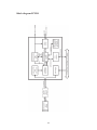
Technical Information
Operating Instructions
DCF77 PCI511
Impressum
Meinberg Funkuhren GmbH & Co. KG
Auf der Landwehr 22
D-31812 Bad Pyrmont
Phone:
Fax:
++49 52 81 - 9309-0
++49 52 81 - 9309-30
Internet: http://www.meinberg.de
Email: info@meinberg.de
May 22, 2006
Table of Contents
Impressum............................................................................................ 2
Driver diskette ..................................................................................... 5
Readme file .......................................................................................... 7
General information about DCF77 ...................................................... 9
Overview ............................................................................................ 10
Pulse outputs ............................................................................ 10
Block diagram PCI511 ............................................................. 11
Connectors and LEDs in the rear panel ................................... 12
Pin assignments of the 9 pin connector ................................... 13
Installing the PCI511 in your computer ............................................ 13
Aligning the antenna .......................................................................... 14
Technical specifications .................................................................... 16
Firmware updates ..................................................................... 18
Replacing the lithium battery .................................................. 18
CE label .................................................................................... 18
Declaration of Conformity ....................................................... 19
Format of the Meinberg Standard time string ......................... 20
PCI511 component layout ........................................................ 21
4
Driver diskette
5
6
Readme file
The driver diskette contains a file called „readme.txt“, which helps installing the
driver correctly. The content of this file is as follows:
Installation Instructions
------------------------Execute Setup.exe and choose the installation directory.
By default, the installation directory is:
C:\Program Files\Meinberg\MbgMon
Then shut down the computer, install the Meinberg radio
clock plug-in board into a free slot and reboot.
Now you are asked to install a driver. The driver file
MEINBERG.INF can be found in the subdirectory Driver\PnP
of the installation directory.
After the installation is complete, start the monitor
program MbgMon. Start the time service, control the state
of the reference clock and configure the device(s).
Copyright (C) Meinberg Funkuhren, Bad Pyrmont, Germany
7
8
General information about DCF77
The radio clocks made by Meinberg receive the signal from the long wave transmitter DCF77. This long wave transmitter installed in Mainflingen near Frankfurt/
Germany transmits the reference time of the Federal Republic of Germany. This time
reference is either the Central European Time (Mitteleuropäische Zeit, MEZ) or the
Central European Summer Time (Mitteleuropäische Sommerzeit, MESZ). The transmitter is controlled by the atomic clock plant at the Federal Physical Technical
Institute (PTB) in Braunschweig/Germany and transmits the current time of day, date
of month and day of week in coded second pulses. Once every minute the complete
time information is available.
At the beginning of every second the amplitude of the high precision 77.5 kHz
carrier frequency is lowered by 75% for a period of 0.1 or 0.2 sec. The length of these
time marks represent a binary coding scheme using the short time mark for logical
zeroes and the long time mark for logical ones. The information on the current date
and time as well as some parity and status bits can be decoded from the time marks of
the 15th up to the 58th second every minute. The absence of any time mark at the 59th
second of a minute signals that a new minute will begin with the next time mark.
Our radio clocks decode the highly accurate information on date and time within a
wide range around Germany. So some of our clocks are installed in Bilbao/Spain as
well as in the city of Umeå in northern Sweden - fully satisfying the requirements of
the users. The radio clocks automatically switch to summertime and back. The
reception of the time information is free of charge and does not need to be registered.
Generally it is important to position the antenna in an optimal way. It should be
mounted at least 30 centimeters away from the clock unit and from solid steel. The
antenna should be aligned at a right angle to the direction of the transmitter (Frankfurt).
Figure: decoding scheme
9
Overview
Because the radio clock PCI511 is designed as an universal board for computers with
PCI bus, operation within 3.3V and 5V systems is possible.
An external ferrit antenna makes the signal from DCF77 available to the on-board
long wave receiver. The demodulated time marks are decoded by the clock´s microprocessor. If no errors are detected in the current time message an additional plausibility check against the previous time message is performed. If that plausibility
check passes, too, the buffered real time clock on the board is synchronized corresponding to the decoded time and date. Optionally, the decoded date and time
information can be converted to another time zone. The time zone setting can be
modified using the monitor program. The current setting is saved permanently on the
radio clock board.
Software running on the computer can read out the date/time/status and some more
information. Access to the board is made via writing to/reading from I/O ports. It is
possible but not necessary to let the board generate periodic hardware interrupts on
the computer bus.
The diskette contains a driver program that keeps the computer´s system time
synchronous to the board time. If the present delivered diskette doesn’t contain a
driver program for the operating system used, it can be downloaded from:
http://www.meinberg.de/english/sw/
Pulse outputs
The radio clock PCI511 generates pulses whenever a new second (P_SEC) or a new
minute (P_MIN) begins. The P_SEC pulse is available with TTL level (0/+5V) and
RS-232 level (-3..12V/+3..12V), the P_MIN signal with TTL level only. If required,
DIL switches can be set up to direct each of the pulses to a corresponding pin of the 9
pin connector in the rear panel.
10
Block diagram PCI511
11
Connectors and LEDs in the rear panel
The rear panel includes the antenna connector, three status LEDs, the BSL button,
and a 9 pin sub D connector (see figure below).
antenna
free run
field strength
modulation
BSL key
RxD
TxD
GND
The LEDs let the user check for proper receiver
operation. The upper, red LED is on if the clock is
not synchronous to DCF77. This LED can only
change when the minute changes (seconds increment from 59 to 0). The brightness of the LED in
the middle depends on the strength of the RF signal. The lower, green LED should be blinking
exactly once per second corresponding to the time
marks from DCF77. If this LED flickers there is
some electrical noise around which prevents the
receiver from decoding the time marks and synchronizing. All information given by these LEDs is
also available via the monitor program.
The BSL button behind the hole in the slot cover
activates the clock's boot strap loader. This mode
of operation is needed if the clock's firmware shall
be updated.
The 9 pin sub D connector is wired to the radio
clock's serial port. Pin assignment can be seen
from the figure beside. This port can not be used as
serial port for the computer. Instead, the clock uses
the port to send out Meinberg's standard time
string in order to control an external display or
some other external device. The string is sent out
once per second, once per minute or if requested by
an incoming ASCII „?“. It is also possible to change the radio clock's board time by sending such a
string towards the clock.
Transmission speed, framing, and mode of operation can be modified using the monitor program.
The string format is described in the section „Technical Specifications“ at the end of this manual.
12
Pin assignments of the 9 pin connector
When the clock is being shipped, only the signals needed for the serial port are gated
to their pins at the 9 pin connector. If another signal shall be available outside the
computer, the corresponding lever of the DIL switch on the board must be set to the
ON position to connect that signal to its associated pin.
Whenever an additional signal is connected through to the rear panel, special
care must be taken to the configuration of the cable used with the connector. If
pins with TTL level and RS-232 levels are connected to each other, the circuits on
the board may be damaged.
The table below shows the assignments of the 9 pin connector and the corresponding levers of the DIL switch:
Pin
Signal
1
+5V
SWITCH
1
2
RxD in (RS-232)
--
3
TxD out (RS-232)
--
4
P_MIN out (TTL)
5
5
GND
--
6
(reserved)
--
7
P_SEC out (RS-232)
3
8
P_SEC out (TTL)
4
9
(reserved)
--
The signals which have no lever of the DIL switch assigned are hard wired to the pins
of the connector. All levers of the DIL switch which are not listed in the table are
reserved and should remain in the OFF position.
Installing the PCI511 in your computer
Every PCI board is a plug&play board. After power-up, the computer's BIOS assigns
resources like I/O ports and interrupt lines to the board, the user does not need to take
care of the assignments. The programs shipped with the board retrieve the settings
from the BIOS.
The computer has to be turned off and its case must be opened. The radio clock can
be installed in any PCI slot not used yet. The rear plane must be removed before the
board can be plugged in carefully. The computer´s case should be closed again and
the antenna connected to the PCI511´s coaxial plug at its rear.
13
Aligning the antenna
Generally, the exact alignment of the antenna is important. It has to be placed in
longitudinal direction to the transmitter (Frankfurt), see arrow printed on the label of
the antenna.
A distance of several meters to TV- or computer monitors, to computers or
microprocessor boards should be kept. These devices can produce interference fields
that lead to a poor or no DCF77 receiption. If it is not possible to mount the antenna
with a sufficient distance to the computer monitor, it’s line frequency should not be
close to the RF-frequency of DCF77 (77.5 kHz).
The antenna should be installed with a minimum distance of 30cm to all metal
objects. Otherwise the ferrite antenna will be detuned and the received power decreases.
Alignment of the antenna can be done by watching the modulation and field
strength LEDs. Like described in chapter „General information about DCF77“, undisturbed pulses per second (except 59. second) without any interfering pulses are
required for corrcect decoding of the DCF77 time telegram. Therefore, a modulation
LED blinking exactly once per second is a criterion for good receiption of the DCFsignal.
Because PCI511 uses a quadrature demodulator as receive circuit, it is possible to
evaluate the field strength of the DCF77 signal only. Interfering signals within the
bandwith of the receiver have no affect on the brightness of the field strength LED
therefore.
If the radio clock is installed in the computer, it may be difficult to use the status
LEDs for alignment of the antenna. Therefore modulation and field strength can be
observed by using the monitor program „MbgMon“ (part of the shipped driver) also.
14
Modulation is displayed as a LED, the DCF77 field strength as a bar graph. Optionally, the modulation signal can be made audible via the speaker of the computer.
The monitor program displays the following window:
modulation
field strength
acoustig modulation
signal on/off
15
Technical specifications
RECEIVER:
Direct conversion quadrature receiver with automatic gain
control
Bandwidth: approx. 20 Hz
ANTENNA:
Active external ferrite antenna in a plastic case
Length of the cable: up to more than 100m
Standard:
BNC type connector, 5m of RG174 cable
Outdoor:
N type connector, RG58 cable
RF AMPLITUDE,
MODULATION: Indicated by LED and on-screen by monitor program
TIMECODE
CHECK:
BATTERY
BACKUP:
Parity and consistency checking over a period of two minutes
RF distortions indicated by both LED and a bit of the
status register
Without RF signal the clock runs on XTAL
with an accuracy of 10-6 (after 1 day of synchronization)
Lithium battery or Gold Cap
when the computer is turned off, the on-board RTC keeps the
time based on XTAL for more than 10 years (lithium battery)
rsp. 150 hours (gold cap)
RELIABILITY OF
OPERATION:
Microprocessor supervisory circuit provides watchdog timer,
power supply monitoring and backup-battery switchover
SYSTEM BUS
INTERFACE:
universal board for 3.3V and 5V systems
32 bit, 33MHz or 66MHz PCI bus
compatible to PCI specifications
DATA FORMAT: Binary, byte serial
16
CONFIGURABLE
TIME ZONES:
Central European Time CET/CEST (default), always CET (no
daylight saving time), UTC, East European Time EET/EEST
(CET/CEST + 1h)
SERIAL
INTERFACE:
PULSEOUTPUTS:
Transmission Speed:
Framing:
Mode of Operation:
300 through 9600 Baud
8N1, 7E2, 8N2, or 8E1
send string per second, per minute,
after request ´?´ received
Output String:
Meinberg standard time string
(described below)
Pulses every second (PPS) with
TTL- and RS232-level, pulse duration 100 msec, active high
Pulses every minute (PPM) with
TTL- level, pulse duration 100 msec, active high
POWER
REQUIREMENT: 5V PCI-bus:
+5V
3.3V PCI-bus:
+5V and +3.3V
Current consumption:
@130 mA
all voltages supplied by PCI-bus
PHYSICAL
DIMENSION:
short PCI expansion board
AMBIENT
TEMPERATURE: 0 ... 70°C
HUMIDITY:
max. 85 %
17
Firmware updates
Whenever the on-board software must be upgraded or modified, the new firmware
can be downloaded to the internal flash memory via the radio clock's serial port
COM0. There is no need to open the computer case and insert a new EPROM.
If the button behind a hole in the rear slot cover is pressed twice, a bootstrap loader
is activated and waits for instructions from the serial port COM0. A loader program
shipped together with the file containing the image of the new firmware sends the
new firmware from one of the computer's serial ports to the clock's serial port COM0.
The bootstrap loader does not depend on the contents of the flash memory, so if the
update procedure is interrupted, it can easily be repeated.
The contents of the program memory will not be modified until the loader program
has sent the command to erase the flash memory. So if the button has been pressed
accidentally, the system will be ready to operate again after the computer has been
turned off an the on again.
Replacing the lithium battery
The life time of the lithium battery on the board is at least 10 years. If the need arises
to replace the battery, the following should be noted:
ATTENTION!
Danger of explosion in case of inadequate replacement of
the lithium battery. Only identical batteries or batteries
recommended by the manufacturer must be used for replacement. The waste battery must be disposed as proposed by the manufacturer of the battery.
CE label
18
Declaration of Conformity
Hersteller
Manufacturer
Meinberg Funkuhren GmbH & Co. KG
Auf der Landwehr 22
D-31812 Bad Pyrmont
erklärt in alleiniger Verantwortung, daß das Produkt
declares under its sole responsibility, that the product
Produktbezeichnung
DCF77 Funkuhr
Product Name
Modell / Typ
PCI511
Model Designation
auf das sich diese Erklärung bezieht, mit den folgenden Normen übereinstimmt
to which this declaration relates is in conformity with the following standards
EN55022, 9/03, Class B
Grenzwerte und Meßverfahren für
Funkstörungen von
informationstechnischen Einrichtungen
Limits and methods of measurement of radio interference
characteristics of information technology equipment
EN55024, 10/03
Grenzwerte und Meßverfahren für
Störfestigkeit von
informationstechnischen Einrichtungen
Limits and methods of measurement of Immunity characteristics of information technology equipment
gemäß den Bestimmungen der Richtlinie 89/336/EWG zur Angleichung der Rechtsvorschriften der Mitgliedstaaten über die elektromagnetische Verträglichkeit.
following the provisions of Directive 89/336/EEC on the approximation of the laws of the Member States
relating to electromagnetic compatibility.
Bad Pyrmont, den 07.06.2006
19
Format of the Meinberg Standard time string
The Meinberg Standard time string is a sequence of 32 ASCII characters starting
with the STX (start-of-text) character and ending with the ETX (end-of-text) character. The format is:
<STX>D:dd.mm.yy;T:w;U:hh.mm.ss;uvxy<ETX>
The letters printed in italics are replaced by ASCII numbers whereas the other
characters are part of the time string. The groups of characters as defined below:
<STX>
Start-Of-Text (ASCII code 02h)
dd.mm.yy the current date:
dd day of month
(01..31)
mm month
(01..12)
yy year of the century (00..99)
w
the day of the week
(1..7, 1 = Monday)
hh.mm.ss
the current time:
hh hours
mm minutes
ss seconds
(00..23)
(00..59)
(00..59, or 60 while leap second)
uv
clock status characters:
u: ‘#’ clock has not synchronized after reset
‘ ‘ (space, 20h) clock has synchronized after reset
v:
different for DCF77 or GPS receivers:
‘*’ DCF77 clock currently runs on XTAL
GPS receiver has not checked its position
‘ ‘ (space, 20h) DCF77 clock is sync'd with transmitter
GPS receiver has determined its position
x
time zone indicator:
‘U’ UTC Universal Time Coordinated, formerly GMT
‘ ‘ MEZ European Standard Time, daylight saving disabled
‘S’ MESZ European Summertime, daylight saving enabled
y
anouncement of discontinuity of time, enabled during last hour
before discontinuity comes in effect:
‘!’ announcement of start or end of daylight saving time
‘A’ announcement of leap second insertion
‘ ‘ (space, 20h) nothing announced
<ETX>
End-Of-Text (ASCII code 03h)
20
PCI511 component layout
21