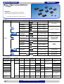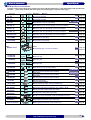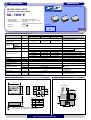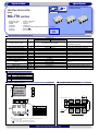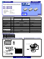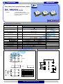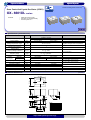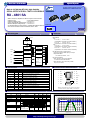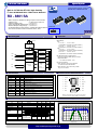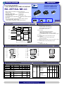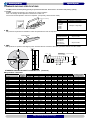
1
Crystal Devices Catalogue '08.10 “QMEMS” EPSON TOYOCOM In order to meet customer needs in a rapidly advancing digital, broadband and ubiquitous society, we are committed to offering products that are one step ahead of the market and a rank above the rest in quality. To achieve our goals, we follow a “3D (three device) strategy” designed to drive both horizontal and vertical growth. We will to grow our three device categories of “Timing Devices”, ”Sensing Devices” and “Optical Devices”, and expand vertical growth through a combination of products from these categories. A Quartz MEMS is any high added value quartz device that exploits the characteristics of quartz crystal material but that is produced using MEMS (micro-electro-mechanical system) processing technology. Market needs are advancing faster than previously imagined toward smaller, more stable crystal products, but we will stay ahead of the curve by rolling out products that exceed market speed and quality requirements. We want to further accelerate the 3D strategy by QMEMS. Quartz devices have become crucial in the network environment where products are increasingly intended for broadband, ubiquitous applications and where various types of terminals can transfer information almost immediately via LAN and WAN on a global scale. Epson Toyocom Corporation addresses every single aspect within a network environment. The new corporation offers “Digital Convergence” solutions to problems arising with products for consumer use, such as, core network systems and automotive systems. PROMOTION OF ENVIRONMENTAL MANAGEMENT SYSTEM CONFORMING TO INTERNATIONAL STANDARDS At Epson Toyocom, all environmental initiatives operate under ISO 14000 is an international standard for environmental management the Plan-Do-Check-Action(PDCA) cycle designed to achieve that was established by the International Standards Organization in 1996 continuous improvements. The environmental management against the background of growing concern regarding global warming, system (EMS) operates under the ISO 14001 environmental destruction of the ozone layer and global deforestation management standard. All of our major manufacturing and non-manufacturing sites,in Japan and overseas, completed the acquisition of ISO 14001 certification. In the future, new group companies will be expected to acquire the certification around the third year of operations. WORKING FOR HIGH QUALITY In order provide high quality and reliable products and services than meet customer needs, Epson Toyocom made early efforts towards obtaining ISO9000 series certification and has acquired ISO9001 for all business establishments in Japan and abroad. We have also acquired ISO/TS 16949 certification that is requested strongly by major automotive manufacturers as standard. QS-9000 is an enhanced standard for quality assurance systems formulated by leading U.S. automobile manufacturers based on the international ISO 9000 series. ISO/TS 16949 is a global standard based on QS-9000, a severe standard corresponding to the requirements from the automobile industry. ►Explanation of the mark that are using it for the catalog ►Pb free. ►Complies with EU RoHS directive. ►Pb free terminal designed. Contains Pb in products exempted by RoHS directive. (Contains Pb in sealing glass, high melting temperature type solder or other.) ►Complies with EU RoHS directive. ►The products have been designed for high reliability applications such as Automotive. Notice ●This material is subject to change without notice. ●Any part of this material may not be reproduced or duplicated in any form or any means without the written permission of Epson Toyocom. ●The information, applied circuitry, programming, usage, etc., written in this material is intended for reference only. Epson Toyocom does not assume any liability for the occurrence of infringing on any patent or copyright of a third party. This material does not authorize the licensing for any patent or intellectual copyrights. ●Any product described in this material may contain technology or the subject relating to strategic products under the control of the Foreign Exchange and Foreign Trade Law of Japan and may require an export license from the Ministry of International Trade and Industry or other approval from another government agency. ●You are requested not to use the products (and any technical information furnished, if any) for the development and/or manufacture of weapon of mass destruction or for other military purposes. You are also requested that you would not make the products available to any third party who may use the products for such prohibited purposes. ●These products are intended for general use in electronic equipment. When using them in specific applications that require extremely high reliability, such as the applications stated below, you must obtain permission from Epson Toyocom in advance. / Space equipment (artificial satellites, rockets, etc.) / Transportation vehicles and related (automobiles, aircraft, trains, vessels, etc.) / Medical instruments to sustain life / Submarine transmitters / Power stations and related / Fire work equipment and security equipment / traffic control equipment / and others requiring equivalent reliability. ● In this new crystal master for Epson Toyocom, product codes and markings will remain as previously identified prior to the merger. Due to the on-going strategy of gradual unification of part numbers, please review product codes and markings, as they will change during the course of the coming months. We apologize for the inconvenience, but we will eventually have a unified part numbering system for Epson Toyocom that will be user friendly. CONTENTS CONTENTS ●Products Information on WWW server ........................................... 2 All lineup ●Crystal Units / Resonator kHz Range Crystal Units .............................................................. 3 MHz Range Crystal Units ............................................................. 4 SAW Resonator ............................................................. 5 ●Oscillator SPXO (Plastic package type) ....................................................... 6 SPXO (Ceramic package type) .................................................... 7 Programmable (SG-8003 series) ................................................. 8 Programmable (SG-8002 series) ................................................. 9 Spread Spectrum.......................................................................... 10 Low Jitter SAW ............................................................................. 11 High Stability / Multi Output .......................................................... 12 VCXO ........................................................................................... 13 TCXO ........................................................................................... 14 OCXO ........................................................................................... 15 Rubidium ...................................................................................... 16 ●Real Time Clock Module Serial Interface (4-Wire/3-Wire).................................................... 17 2 Serial Interface (I C_ Bus)............................................................ 18 Parallel Interface .......................................................................... 19 ●Filter Monolithic Crystal Filter (MCF)..................................................... 20 SAW Filter .................................................................................... 20 ●Optical Device ................................................................................ 21 Wave Plate Dichroic Prism Trichroic Prism Grating Dichroic Filter OLPF (OPTICAL LOW PASS FILTER) Heat Sink plate Etalon Filter PBS Prism PS Converter ●Sensor ............................................................................................ 22 Gyro Sensor Temperature Sensing Crystal Pressure Sensing Crystal Products Information ●FC-125 ........................................ ●FC-13E........................................ ●FA-118T ...................................... ●SG-150 **E(SEE,SDE,SCE) ....... ●SG-211 **E(SEE,SDE,SCE) ....... ●SG-210 **D(SED,SDD,SCD) ...... ●SG-210 series ............................. ●SG-770 series ............................. ●SG-771PCD ................................ 24 25 26 27 28 29 30 31 32 ●SG-8003 series............................ ●VG-4231CB/VG-4531CB ............. ●VG-4501CA/VG-4502CA............. ●VG-4511CA ................................. ●TG-5021BA.................................. ●OX-6501GG................................. ●OX-6502GG................................. ●OX-6601DL.................................. ●Rb-3310N .................................... 33 35 36 37 38 39 40 41 42 ●Rb-2110CB.................................. ●RA-4565SA ................................. ●RX-4801SA ................................. ●RX-8801SA ................................. ●RX-8571series............................. ●XV-8000LK .................................. ●OLPF ........................................... Application Guide ●Working for Pb Free......................................................................... ●Handling precautions ....................................................................... ●Precaution in designing oscillation circuits....................................... ●Output waveform and test circuit ..................................................... ●Standard packing specifications....................................................... ●Glossary........................................................................................... ●Manufacturing Plant / Business area ............................................... http://www.epsontoyocom.co.jp 50 ~ 52 53 ~ 55 56 57 ~ 58 59 ~ 61 62 ~ 64 65 1 43 44 45 46 47 48 49 WWW server Epson Toyocom ■ Products Information on WWW server Epson toyocom is providing the Products Information, timing device, sensing device, optical device and more. Please access here ! Epson Toyocom Home Page http://www.epsontoyocom.co.jp Lineup Page for each device Data Sheet page ■ Product Inquiry by E-Mail Epson Toyocom receives your inquiries on the products through e-mail. 2 http://www.epsontoyocom.co.jp Crystal unit Epson Toyocom Ɣ)HDWXUHV Ź3KRWROLWKRJUDSK\ILQLVKHGDOORZVXQLIRUPDQGVWDEOH SHUIRUPDQFH Ź0DQ\SURGXFWOLQHXSVWRDQXOWUDVPDOOVL]H60'W\SHDQG F\OLQGHUW\SH ŶN+]5DQJH&U\VWDO8QLW7XQLQJIRUN N+]5DQJH&U\VWDO8QLW 0RGHO $FWXDOVL]HPP0D[ )UHTXHQF\ N+] N+] N+] N+] N+] )&0 )& )&( )&) )& )& )& 0& 0& îîW ƔN+] ƔN+] ƔN+] îîW N+] N+] 0& îîW N+] N+] 0& îîW N+] N+] 0&$ îîW N+] N+] &5 îîW N+] N+] îîW îîW ƔN+] îîW îîW N+] N+] îîW îîW ĭ &5; &5 ĭ &5 &7<3( ĭ ĭ &7<3( ĭ ƔN+] ĭ N+] N+] N+] N+] Ź6SHFLILFDWLRQN+] ,WHP 0RGHO )&0 )& )&( )&) )& )& )& 0& 0& 0& 0&$ 0& 0& &5 &5; &5 &5 )& 0& 0& 0& 0&$ 0& 0& &7<3( &7<3( ƔN+] )UHTXHQF\WROHUDQFH 6WDQGDUG )UHTXHQF\YHUVXV WHPSHUDWXUHFKDUDFWHULVWLFV 0RWLRQDO UHVLVWDQFH 0D [ /RDG FDSDFLWDQFH (6WDQGDUG) 6WRUDJH WHPSHUDWXUH 2SHUDWLQJ WHPSHUDWXUH IBQRP IBWRO 7XUQRYHUWHPSHUDWXUH7L &7\S 5 &/ 7BVWJ 7BXVH Nȍ Nȍ Nȍ Nȍ Nȍ Nȍ Nȍ S) S) S)S) S) S) S) &WR& &WR& î î îî î î î N+] î î 3DUDEROLFFRHIILFLHQW% î&0D [ IBWHP %7Lnș[ î 1RPLQDOIUHTXHQF\UDQJH )UHTXHQF\WROHUDQFH 6WDQGDUG IBQRP IBWRO )&0 )& ƔN+] 1RPLQDOIUHTXHQF\ Ź6SHFLILFDWLRQN+]5$1*( ,WHP 0RGHO ƔN+] N+]WRN+] )UHTXHQF\YHUVXV WHPSHUDWXUHFKDUDFWHULVWLFV 7XUQRYHUWHPSHUDWXUH7L Nȍ S) Nȍ NȍNȍ Nȍ Nȍ S)WR &WR& &WR& 0RWLRQDO UHVLVWDQFH 0D [ /RDG FDSDFLWDQFH (6WDQGDUG) 6WRUDJH WHPSHUDWXUH 2SHUDWLQJ WHPSHUDWXUH 7BVWJ 7BXVH &WR& &WR& &WR& &WR& 5 &/ NȍWRNȍ î NȍWRNȍ S) S) S) S) S)S) S)S) S) &7\S î îî N+]WRN+]N+] N+]WRN+]N+] N+]WRN+]N+] S)S) S)S) S) îî N+]WRN+] N+]WRN+] Nȍ NȍWRNȍ 3DUDEROLFFRHIILFLHQW% î&0D [ IBWHP %7Lnș[ NȍWRNȍ NȍWRNȍ NȍWRNȍ S) NȍWRNȍ îîî îî NȍWRNȍ NȍWRNȍ S)WR KWWSZZZHSVRQWR\RFRPFRMS Crystal unit Epson Toyocom MHz Range Crystal Unit ●Features ►The most popular AT cut crystal units. ►Miniaturization is materialized with the processing method that be unique. ■MHz Range Crystal Unit (AT) Model Actual size (mm) Max. FA-128 Frequency 1 MHz 10 MHz 20 MHz 2.0×1.6×0.5 t FA-20H 2.5×2.0×0.55 t FA-238V 3.2×2.5×0.7 t FA-238 3.2×2.5×0.7 t FA-23A 3.2×2.5×0.8 t TSX-3225 3.2×2.5×0.6 t TSX-4025 4.0×2.5×0.7 t TSX-5032 5.0×3.2×0.8 t FA-365 24 MHz 8.0×3.8×2.54 t MA-406 11.7×4.8×3.7 t MA-505/506 13.46×5.08×4.6 t CA-301 Φ3.1 Model Actual size (mm) 3.8×3.8×1.0 t (Max.) FH-33H 54 MHz 48 MHz 50 MHz,52 MHz 12 MHz ●● 12 MHz 15.999 MHz 16 MHz 60 MHz 12 MHz 54 MHz 16 MHz 48 MHz 12 MHz 32 MHz 10 MHz 32 MHz ●12 MHz 6.0×3.5×1.4 t MA-306 64 MHz 14 MHz 41 MHz ●14.31818 MHz 17.734 MHz 41 MHz 4 MHz 64 MHz* * 8.0 MHz <f< 8.2 MHz : Unavailable. Available frequency from 4 MHz to less than 5.5 MHz (4 MHz ,4.032 MHz ,4.096 MHz ,4.19 MHz ,4.194304 MHz , 4.433619 MHz ,4.5 MHz ,4.8 MHz ,4.9152 MHz) Frequency 50 MHz 100 MHz 200 MHz 60 MHz 500 MHz 230 MHz ►Specifications Item Model Nominal frequency range Frequency tolerance (Standard) f f_tol FA-128 24 MHz to 54 MHz FA-20H 12 MHz to 48 MHz 50 MHz,52 MH z FA-238V 12 MHz to 15.999 MH z -6 ±10×10 ,±30×10 -6 -6 -6 ±10×10 ,±30×10 ±50×10 -6 -6 Frequency versus temperature characteristics (Operating temperature) Motional resistance (Ma x.) Load capacitance (Standard) Storage temperature Operating temperature f_tem R1 CL T_stg T_use 60 Ω to 80 Ω 8 pF to ∞ -40 °C to +125 °C -40 °C to +85 °C 40 Ω to 150 Ω 9 ,10,12,16 pF,∞ -40 °C to +125 °C -40 °C to +85 °C 80 Ω to 100 Ω 10 pF -40 °C to +125 °C -40 °C to +85 °C 40 Ω to 80 Ω 10 pF -40 °C to +125 °C -40 °C to +85 °C 40 Ω to 200 Ω 9,12,16 pF, ∞ -40 °C to +125 °C -40 °C to +125 °C 9,12,16 pF, ∞ -40 °C to +125 °C -20 °C to +75 °C -55 °C to +125 °C -20 °C to +70 °C ±10 × 10-6,±30 × 10-6 ( -20 °C to +75 °C) ±10 × 10-6,±30 × 10-6 ( -20 °C to +75 °C) ±30 × 10-6 ( -20 °C to +70 °C) ±30 × 10-6 ( -20 °C to +70 °C) ±20 × 10-6 ( -40 °C to +85 °C) ±50 × 10-6 ( -40 °C to +125 °C) FA-238 16 MHz to 60 MHz ±50×10 FA-23A 12 MHz to 54 MHz ±10×10-6,±20×10-6 TSX-3225 TSX-4025 TSX-5032 16 MHz to 48 MHz 12 MHz to 32 MHz 10 MHz to 32 MHz ±10×10-6 ±10×10-6 ( -20 °C to +75 °C) 40 Ω to 60 Ω FA-365 12MHz,14 MH z to 41 MH z ±50×10 -6,±100×10-6 ±30 × 10-6 ( -20 °C to +70 °C) 50 Ω to 60 Ω MA-306 14.31818 MHz, 17.734 MHz to 41 MH z ±30 × 10-6 ( -20 °C to +70 °C) 60 Ω ±30 × 10-6,±50 × 10-6 ( -20 °C to +70 °C) 40 Ω to 150 Ω MA-406 4 MH z to 64 MH z MA-505 MA-506 4 MH z to 64 MH z CA-301 4 MH z to 64 MH z FH-33H 60 MHz to 230 MH z 4 ±50×10 -55 °C to +100 °C -6 ±30×10-6 (±50×10-6,±100×10-6) ±35×10 10 pF to ∞ -6 -6 -6 ±30 × 10 ,±50 × 10 ( -20 °C to +70 °C) ±20 × 10-6 ( -40 °C to +85 °C) 40 Ω to 150 Ω 30 Ω to 40 Ω http://www.epsontoyocom.co.jp Fundamental: 10 pF to ∞ 3ed Overtone: 5 pF to ∞ 17 pF to ∞ -55 °C to +125 °C -20 °C to +70 °C -40 °C to +85 °C -50 °C to +95 °C -40 °C to +85 °C Crystal Unit Epson Toyocom SAW Resonator ●Features ►Crystal resonator with surface acoustic wave. ►Photolithography finished allows uniform and stable performance. ■Resonator (SAW) Model Actual size (mm) Typ. Frequency 200 MHz 500 MHz 700 MHz 1 GHz NS-21R 2.5×2.0×0.86 t 300 MHz NS-32R 3.8×3.8×0.98 t 312 MHz 870 MHz FS-335 3.8×3.8×0.98 t 300 MHz 870 MHz FS-555 4.8×5.2×1.5 t FS-585 4.8×5.2×1.5 t 500 MHz 230 MHz 500 MHz 300 MHz 500 MHz ►Specifications Item Nominal frequency range Model Frequency tolerance (Standard) Frequency versus temperature characteristics Motional resistance (Ma x.) Harmonic ratio (standard) Storage temperature Operating temperature RS / R1 T_stg T_use -40 °C to +85 °C -40 °C to +85 °C -40 °C to +125 °C -40 °C to +120 °C f_nom f_tol Parabolic coefficient (B) R1 NS-21R 300 MHz to 500 MH z ±50×10-6,±100×10-6,±150×10-6 -(1.6±0.4) ×10-8 / °C2 20 Ω NS-32R 312 MHz to 870 MH z ±50×10-6,±100×10-6 -(1.6±0.4) ×10-8 / °C2 30 Ω FS-335 300 MHz to 870 MH z FS-555 230 MHz to 500 MH z ±50×10-6,±100×10-6 -(3.4±0.8) ×10-8 / °C2 25 Ω to 40 Ω FS-585 300 MHz to 500 MH z ±50×10-6,±100×10-6 -8 2 -(3.4+0.8) ×10 / °C 2 Min. 18 Ω -(3.4-0.6) ×10-8 / °C2 Bits of knowledge The temperature characteristic of the SAW resonator becomes the quadratic curve. It is the same temperature characteristic as a tuning fork crystal unit. The inclination of the curve changes by the thickness and width of the electrode. The SAW resonator needs the advanced design for the electrode pattern. The SAW resonator (NS series) of Epson Toyocom optimizes design conditions and provides a higher temperature characteristic. SAW resonator Frequency -6 f_tol(1×10 ) 0 SAW resonator of temperature characteristic. -20 -30 -40 -50 -60 2 Use the appro ximate e xpression o n ca lculatio n. f_te m=B(Ti-θX) -10 -8 B — --- : Parabolic coefficient -(1.6±0.4 ) ×10 / °C -6 2 → -0.02 × 10 / °C Max. Ti : Turno ver temperature (+25 °C) ΘX : Specified te mperature (e xamp le : +50 °C) NS series FS series Typical Ti=+25 ℃ 2 -6 -0.02×(25-50) =-12.5×10 (Te mperature cha racteristic o f 50°C become -70 2 -6 -12.5×10 ) -20 -10 0 10 20 30 40 50 60 70 Temperature (°C) http://www.epsontoyocom.co.jp 5 Crystal Oscillator Epson Toyocom CRYSTAL OSCILLATOR SPXO (Plastic package type) ●Features Features ►Built-in heat resistive crystal unit provides heat resistance equivalent to that of general-purpose ICs. ►Low current consumption by output enable function (OE) or standby function ( ST ). ■SPXO Plastic package type Model Frequency 1 Hz 1 MHz Actual size (mm) SG-3030JC SG-3040JC 10.5×5.8×2.7 t (Max.) SG-3030JF 7.1×5.1×1.5 t (Max.) SG-3030LC SG-3040LC 3.6×2.8×1.2 t (Max.) SG-150 series 2.1×1.7×0.75 t (Typ.) 3 MHz SG-550 series 5.0×3.2×1.2 t (Max.) 2 MHz SG-645 series 7.1×5.1×1.5 t (Max.) SG-636 series 10.5×5.8×2.7 t (Max.) 50 MHz 100 MHz 500 MHz 800 MHz ●32.768 kHz 54 MHz 48 MHz 32.001 MHz 135 MHz 2.21675 MHz 135 MHz 1.025 MHz 135 MHz SG-615 series 14.0×9.8×4.7 t (Max.) SG-531 series DIP half size SG-51 series DIP full size 1.025 MHz 66.667 MHz ►Specifications Item Model SG-3030LC/JF/JC SG-3040LC/JC SG-150 SEE SG-150 SDE Output frequency range Frequency tolerance (Temperature range) Operating temperature Current consumption Supply voltage Output load condition Output control 32.768 kHz 5±23 × 10-6 -40 °C to +85 °C -40 °C to +85 °C 2 µA Max. 3.1 µA Max. 1.5 V to 5.5 V 0.9 V to 3.6 V 15 pF VIO VIO 3 MH z to 54 MH z ±15 × 10 ±20 × 10-6 -20 °C to +70 °C -40 °C to +85 °C 4.5 mA Max. 5 mA Max. 2.25 V to 2.7 V 15 pF ST 6 mA Max. 2.7 V to 3.6 V -6 15 pF ST -6 SG-150 SCE SG-550 SEF SG-550SDF SG-550SCF SG-645PTW/STW SG-645PHW/SHW 2 MH z to 48 MH z ±50 × 10 ±100 × 10-6 -20 °C to +70 °C -40 °C to +85 °C 32.001 MHz to 135 MHz ±50 ,±100 × 10-6 (-20 °C to +70 °C) ±100 × 10-6 (-40 °C to +85 °C) -20 °C to +70 °C (-40 °C to +85 °C) SG-645PCW/SCW SG-636PTF 2.21675 MHz to 41 MHz SG-636PH SG-636PCE/SCE 41.001 MHz to 70 MH z -20 °C to +70 °C 32.001 MHz to 135 MHz SG-636PHW/SHW SG-636PCW/SCW SG-51/531/615P SG-51/531/615PTJ SG-51/531/615PH SG-531/615PTW/STW 2.21675 MHz to 33 MHz 1.025 MHz to 26 MH z 26.001 MHz to 66.667 MH z 55.001 MHz to135 MH z ±50 ,±100 × 10-6 26.001 MHz to 135 MHz SG-531/615PCG/SCG SG-615PCN 1.5 MH z to 26 MH z 26.001 MHz to 66.667 MH z (-20 °C to +70 °C) ±100 × 10-6 (-40 °C to +85 °C) *1 -20 °C to +70 °C -20 °C to +70 °C (-40 °C to +85 °C) *1 Except : PTW, STW, PHW, SHW 6 2.2 V to 3.0 V 2.7 V to 3.6 V 45 mA Ma x. 4.5 V to 5.5 V 5 TTL 15 pF 28 mA Ma x. 3.0 V to 3.6 V 15 pF 5.0 V±0.5 V 3.3 V±0.3 V 5 mA Max. 2.5 V±0.25 V 45 mA Ma x. 5.0 V±0.5 V 28 mA Ma x. 3.3 V±0.3 V 25 mA Ma x. 4.5 V to 5.5 V 12 mA Ma x. 2.7 V to 3.6 V 23 mA Ma x. -6 ±50 × 10 ±100 × 10-6 SG-531/615PHW/SHW SG-531/615PCW/SCW *1 ±50 × 10-6 ±100 × 10-6 SG-636PTG/PHG SG-636PCG/SCG 1.6 V to 2.2 V 35 mA Ma x. 9 mA Max. 2.21675 MHz to 40 MHz SG-636PDE SG-636PTW/STW 3 mA Max. 3.5 mA Max. 4.5 mA Max. 17 mA Ma x. -6 ±100 × 10 1.6 V to 2.2 V http://www.epsontoyocom.co.jp 35 mA Ma x. 10 TTL, 50 pF 15 pF 30 pF OE OE/ ST 15 pF 5 TTL OE 15 pF 15 pF OE/ ST 25 pF 10TTL, 50 pF 5 TTL 5.0 V±0.5 V OE/ ST OE ST OE 50 pF 5 TTL 45 mA Ma x. 28 mA Ma x. 3.3 V±0.3 V 15 pF 15 pF 12 mA Ma x. 2.7 V to 3.6 V 25 pF 20 mA Ma x. 3.0 V to 3.6 V 15 pF OE/ ST OE Crystal oscillator Epson Toyocom CRYSTAL OSILLATOR SPXO (Ceramic package type) ●Features ►High-density mounting-type SMD. ►Low current consumption by output enable function (OE) or standby function ( ST ). ■SPXO Ceramic package type Model Frequency 1 Hz 1 MHz Actual size (mm) Typ. 50 MHz 100 MHz SG-211 series 2.5×2.0×0.7 t 2.375 MHz SG-210 series 2.5×2.0×0.8 t 2 MHz SG-310 series 3.2×2.5×1.05 t 2 MHz 80 MHz TCO-710x series SG-710 series 5.0×3.2×1.0 t 1.5 MHz 75 MHz SG-770 series SG-771 PCD 230 MHz 80 MHz 7.0×5.0×1.6 t TCO-708x series 125 MHz 50 MHz 7.0×5.0×1.6 t 175 MHz 1.5 MHz 7.0×5.0×1.6 t 800 MHz 48 MHz 1.8 MHz 7.3×4.8×1.3 t 500 MHz 60 MHz 160 MHz ►Specifications Item Model SG-211SEE SG-211SDE SG-211SCE SG-210SGB Output frequency range Frequency tolerance (Temperature range) 2.375 MHz to 60 MH z ±15 × 10 ±20 × 10-6 -40 °C to +85 °C -20 °C to +70 °C -6 -6 2 MH z to 32 MH z ±50 × 10 Operating temperature Current consumption Supply voltage 4.5 mA Max. 5 mA Max. 1.6 V to 2.2 V 2.2 V to 2.7 V 6 mA Max. 2.7 V to 3.6 V -40 °C to +85 °C 1.0 mA Max. 1.3 V to 1.7 V SG-210SEB ±50,±100 × 10-6 ±100,±150 × 10-6 -40 °C to +85 °C -40 °C to +125 °C 1.6 mA Max. 2.0 mA Max. 1.6 V to 2.2 V SG-210SDB ±50,±100 × 10-6 ±100,±150 × 10-6 -40 °C to +85 °C -40 °C to +125 °C 2.4 mA Max. 3.0 mA Max. 2.2 V to 3.0 V ±50,±100 × 10-6 ±100,±150 × 10-6 -40 °C to +85 °C -40 °C to +125 °C 3.0 mA Max. 4.0 mA Max. 2.7 V to 3.6 V 3.0 mA Max. 3.5 mA Max. 1.6 V to 2.2 V 2.2 V to 3.0 V 4.5 mA Max. 2.7 V to 3.6 V 6.0 mA Max. 2.2 V to 2.7 V 2 MH z to 48 MH z SG-210SCB SG-310SEF SG-310SDF ±50,±100 × 10-6 (-20 °C to +70 °C) ±100 × 10-6 (-40 °C to +85 °C) ±20 ,±25 ,±50 ,±100 × 10-6 2 MH z to 48 MH z SG-310SCF SG-310SDN 3 MH z to 80 MH z SG-310SCN -30 °C to +85 °C -40 °C to +85 °C ±20 ,±25 ,±50 ,±100 × 10-6 ±20 ,±25 × 10-6 -20 °C to +70 °C -30 °C to +85 °C -6 TCO-7106X1A TCO-7107X1A TCO-7106X1A1 ±100 × 10-6 ±50 × 10-6 1.5 MH z to 75 MH z ±100 × 10-6 ±50 × 10-6 -6 TCO-7107X1A2 TCO-7106X1A4 ±100 × 10 ±50 × 10-6 TCO-7107X1A4 SG-710PTK 1.8 MH z to 50 MH z SG-710PHK 1.8 MH z to 80 MH z SG-710ECK 1.8 MH z to 125 MHz ±100 × 10-6 ±25 ,±50 ,±100 × 10-6 (-10 °C to +70 °C) ±50 ,±100 × 10-6 (-40 °C to +85 °C) SG-770SDD SG-770SCD SG-771 PCD TCO-7085X1A* TCO-7086X1A* 50 MHz to 230 MH z 80 MHz to 175 MH z 1.5 MH z to 160 MHz ±50 × 10 ±50 × 10 20 mA Ma x. 3.3 V±0.33 V 15 pF ST 15 pF ST 15 pF ST -40 °C to +85 °C 24 mA Ma x. -10 °C to +70 °C (-40 °C to +85 °C) 40 mA Ma x. 5.0 V±0.5 V http://www.epsontoyocom.co.jp OE 50 pF 3.3 V±0.3 V 15 pF ST LV-PECL ST LV-PECL OE 15 pF ST 15 pF ST 3.3 V±0.165 V 3.3 V±0.165 V 0 °C to +70 °C -10 °C to +70 °C -20 °C to +70 °C -40 °C to +85 °C 10 TTL 30 mA Ma x. 70 mA Ma x. 20 mA Ma x. ±100 × 10-6 ST -20 °C to +70 °C -10 °C to +70 °C 0 °C to +70 °C -10 °C to +70 °C -20 °C to +70 °C -40 °C to +85 °C ±25 × 10-6 ±50 × 10-6 15 pF -10 °C to +70 °C 90 mA Ma x. TCO-7085D1A* TCO-7086D1A* ST 0 °C to +70 °C 0 °C to +70 °C ±100 × 10-6 TCO-7087D1A* 2.7 V to 3.6 V -6 TCO-7087X1A* 1.5 MH z to 75 MH z 7.0 mA Max. 2.5 V±0.125 V 3.3 V±0.165 V -6 15 pF -40 °C to +85 °C -6 ±20 × 10 ±25 × 10-6 Output control -20 °C to +70 °C ±20 ,±25 × 10-6 ±20 ,±25 ,±100 × 10-6 ±20 ,±25 ,±100 × 10 ±50 × 10-6 TCO-7107X1A1 TCO-7106X1A2 -20 °C to +70 °C (-40 °C to +85 °C) Output load condition (1.5 to 75 MHz) 50 mA Ma x. (75 to 160 MHz) 20 mA Ma x. (1.5 to 30 MHz) 40 mA Ma x. (30 to 75 MHz) 3.3 V±0.33 V 3.3 V±0.33 V 5.0 V±0.25 V 5.0 V±0.5 V 5.0 V±0.5 V 7 Crystal oscillator Epson Toyocom CRYSTAL OSCILLATOR Programmable type SG-8003 series ●Features ►Wide frequency output by PLL technology. Short mass production lead time and sample lead time. ►SG-Writer available purchase. ■Programmable type Actual size (mm) Model Supply voltage SG-8003BA 2.1×1.7×0.75 t (Typ.) SG-8003CE 3.2×2.5×1.05 t (Typ.) SG-8003LB 5.0×3.2×1.2 t (Max.) SG-8003JF 7.1×5.1×1.5 t (Max.) SG-8003CA 7.0×5.0×1.4 t (Typ.) SG-8003JC 10.5×5.8×2.7 t (Max.) SG-8003JA 14.0×9.8×4.7 t (Max.) SG-8003DC DIP half size SE/PE 1.6 V to 2.2 V SD/PD 2.2 V to 2.7 V SC/PC 2.7 V to 3.6 V SE/PE 1.6 V to 2.2 V SD/PD 2.2 V to 2.7 V SC/PC 2.7 V to 3.6 V SE/PE 1.6 V to 2.2 V SD/PD 2.2 V to 2.7 V SC/PC 2.7 V to 3.6 V SE/PE 1.6 V to 2.2 V SD/PD 2.2 V to 2.7 V SC/PC 2.7 V to 3.6 V SE/PE 1.6 V to 2.2 V SD/PD 2.2 V to 2.7 V SC/PC 2.7 V to 3.6 V SE/PE 1.6 V to 2.2 V SD/PD 2.2 V to 2.7 V SC/PC 2.7 V to 3.6 V SE/PE 1.6 V to 2.2 V SD/PD 2.2 V to 2.7 V SC/PC 2.7 V to 3.6 V SE/PE 1.6 V to 2.2 V SD/PD 2.2 V to 2.7 V SC/PC 2.7 V to 3.6 V Frequency tolerance Operating temperature B,C,M,L B,C,M,L B,C,M,L B,C,M,L B,C,M,L B,C,M,L B,C,M,L B,C,M,L Frequency 1 Hz 1 MHz 50 MHz 100 MHz 1.0 MHz 166 MHz 1.0 MHz 166 MHz 1.0 MHz 166 MHz 1.0 MHz 166 MHz 1.0 MHz 166 MHz 1.0 MHz 166 MHz 1.0 MHz 166 MHz 1.0 MHz 166 MHz Frequency tolerance : B:±50×10-6(-20 °C to +70 °C ), C:±100×10-6 (-20 °C to +70 °C ), M:±100×10-6 (-40 °C to +85 °C ), L:±50×10-6 (-40 °C to +85 °C ) ►Specifications Item Model Output frequency range Frequency tolerance (Temperature range) Operating temperature 1 MH z to 166 MHz ±50 ,±100 × 10-6 (-20 °C to +70 °C) ±50 ,±100 × 10-6 (-40 °C to +85 °C) -20 °C to +70 °C (-40 °C to +85 °C) PE/SE SG-8003 series PD/SD PC/SC *1 OE function : PE,PD,PC 8 ST function : SE,SD,SC http://www.epsontoyocom.co.jp Current consumption Supply voltage 10 mA Ma x. 1.6 V to 2.2 V 2.2 V to 2.7 V 15 mA Ma x. 2.7 V to 3.6 V Output load condition Output Control *1 15 pF OE/ ST Crystal oscillator Epson Toyocom CRYSTAL OSCILLATOR Programmable type SG-8002 series ●Features ►Wide frequency output by PLL technology. Short mass production lead time and sample lead time. ►SG-Writer available purchase. ■Programmable type Actual size (mm) Model Supply voltage Frequency tolerance Operating temperature B,C M PT/ST PH/SH PC SC 4.5 V to 5.5 V 3.0 V to 3.6 V (2.7V to 3.6 V) PH/SH 5.0 V ±0.5 V PC/SC 3.3 V ±0.3 V B,C,M,L B,C 4.5 V to 5.5 V 3.0 V to 3.6 V (2.7V to 3.6 V) M 7.1×5.1×1.5 t (Max.) PT/ST PH/SH PC SC 7.0×5.0×1.4 t (Typ.) PT/ST PH/SH PC SC 4.5 V to 5.5 V 3.0 V to 3.6 V (2.7V to 3.6 V) PT/ST PH/SH PC SC 4.5 V to 5.5 V 3.0 V to 3.6 V (2.7V to 3.6 V) 14.0×9.8×4.7 t (Max.) PT/ST PH/SH PC SC 4.5 V to 5.5 V 3.0 V to 3.6 V (2.7V to 3.6 V) DIP half size PT/ST PH/SH PC SC 4.5 V to 5.5 V 3.0 V to 3.6 V (2.7V to 3.6 V) DIP full size PT/ST PH/SH PC SC 4.5 V to 5.5 V 3.0 V to 3.6 V (2.7V to 3.6 V) SG-8002CE 3.2×2.5×1.05 t (Typ.) SG-8002LB 5.0×3.2×1.2 t (Max.) SG-8002JF SG-8002CA SG-8002JC 10.5×5.8×2.7 t (Max.) SG-8002JA SG-8002DC SG-8002DB -6 Frequency 1 Hz 1 MHz 1.0 MHz 1.0 MHz 50 MHz 100 MHz 125 MHz 27 MHz 1.0 MHz 125 MHz (2.7 V to 3.6V:1.0MHz to 66.7 MHz) B,C,M B,C M,L 1.0 MHz 80 MHz 1.0 MHz 27 MHz 1.0 MHz 125 MHz (2.7 V to 3.6V:1.0MHz to 66.7 MHz) 1.0 MHz 125 MHz 1.0 MHz 40 MHz 1.0 MHz 125 MHz (2.7 V to 3.6V:1.0MHz to 66.7 MHz) B,C,M B,C M 1.0 MHz 1.0 MHz B,C,M 1.0 MHz 125 MHz (2.7 V to 3.6V:1.0MHz to 66.7 MHz) 125 MHz 55 MHz 1.0 MHz 125 MHz B,C 1.0 MHz 125 MHz (2.7 V to 3.6V:1.0MHz to 66.7 MHz) B,C B,C 1.0 MHz 125 MHz 1.0 MHz 55 MHz 1.0 MHz 125 MHz (2.7 V to 3.6V:1.0MHz to 66.7 MHz) M B,C,M B,C 1.0 MHz 125 MHz 1.0 MHz 55 MHz 1.0 MHz 125 MHz (2.7 V to 3.6V:1.0MHz to 66.7 MHz) M B,C,M B,C M 1.0 MHz 1.0 MHz 1.0 MHz 125 MHz (2.7 V to 3.6V:1.0MHz to 66.7 MHz) B,C,M -6 125 MHz 55 MHz -6 Frequency tolerance : B:±50×10 (-20 °C to +70 °C ), C:±100×10 (-20 °C to +70 °C ), M:±100×10 (-40 °C to +85 °C ), L:±50×10-6 (-40 °C to +85 °C ) ►Specifications Model SG-8002CE Item Output frequency range PT/ST ±50 ,±100 × 10-6 PH/SH (-20 °C to +70 °C) ±100 × 10-6 (-40 °C to +85 °C) 1 MH z to 125 MHz PC/SC PH/SH SG-8002LB PC/SC 1 MH z to 80 MH z 1 MH z to 125 MHz PT/ST SG-8002CA/JF/JA/JC/DB/DC PH/SH 1 MH z to 125 MHz PC/SC *1 *2 Frequency tolerance (Temperature range) Except : JC OE function : PE,PD,PC,PT,PH ST Operating temperature -20 °C to +70 °C (-40 °C to +85 °C) ±50 ,±100 × 10-6 (-20 °C to +70 °C) ±50 ,±100 × 10-6 (-40 °C to +85 °C) ±50 ,±100 × 10-6 -20 °C to +70 °C (-40 °C to +85 °C) (-20 °C to +70 °C) ±100 × 10-6 *1 (-40 °C to +85 °C) -20 °C to +70 °C (-40 °C to +85 °C) Current consumption Supply voltage 40 mA Ma x. 4.5 V to 5.5 V 28 mA Ma x. 2.7 V to 3.6 V 30 mA Ma x. 4.5 V to 5.5 V 28 mA Ma x. 2.7 V to 3.6 V 45 mA Ma x. 4.5 V to 5.5 V 28 mA Ma x. 2.7 V to 3.6 V Output Control *2 Output load condition 5TTL OE/ ST 15 pF 15 pF OE/ ST 5 TTL 15 pF OE/ ST 15 pF function : SE,SD,SC,ST,SH http://www.epsontoyocom.co.jp 9 Crystal oscillator Epson Toyocom CRYSTAL OSCILLATOR Spread Spectrum ●Features ►Support the EMI measure with the SS (Spread spectrum) function. ■Spread Spectrum Model Actual size (mm) SG-9001 LB 5.0×3.2×1.2 t (Max.) SG-9001 CA 7.0×5.0×1.4 t (Typ.) SG-9001 JC 10.5×5.8×2.7 t (Max.) Frequency 1 Hz 1 MHz 10 MHz 50 MHz 100 MHz 135 MHz 500 MHz 10 MHz 166 MHz 10 MHz 166 MHz 800 MHz ►Spread Spectrum Item Output frequency range Frequency tolerance Operating temperature Current consumption Supply voltage Output load condition Output control – -20 °C to +70 °C 30 mA Ma x. 3.3 V±0.3 V 15 pF OE Model SG-9001LB 10 MHz to 135 MH z SG-9001CA/JC 10 MHz to 166 MH z *1 SG-9001CA : The “SS ON/OFF” function is attached. Bits of knowledge Reducing the EMI level with spectrum spreading against the nominal and higher harmonics frequencies by appling the frequency modulation among the indicated frequency domain on the output frequency. Two type of spread spectrum, ”Center Spread” and “Down Spread” are available. The example of both spread spectrum type is shown below. Frequency (MHz) 10 Down SS OFF SS OFF SS ON SS ON dB dB Center Frequency (MHz) http://www.epsontoyocom.co.jp Crystal oscillator Epson Toyocom CRYSTAL OSCILLATOR Low-jitter SAW Oscillator ●Features ►Low-jitter SAW oscillator with SAW. ■Low jitter SAW Model XG-1000CA 7.0×5.0×1.2 t XG-1000CB 5.0×3.2×1.1 t EG-2021CA (2.5 V CMOS) EG-2001CA (3.3 V CMOS) EG-2002CA (3.3 V LV-TTL) EG-2121CA EG-2102CA Frequency 1 Hz 1 MHz 50 MHz 50 MHz Actual size (mm) Typ. 50 MHz 170 MHz 62.5 MHz 7.0×5.0×1.2 t 800 MHz 250 MHz 106.25 MHz 7.0×5.0×1.2 t 500 MHz 170 MHz 62.5 MHz 7.0×5.0×1.2 t Differential LV-PECL LVDS Differential LV-PECL LVDS 100 MHz 170 MHz 170 MHz 53.125 MHz 500 MHz 7.0×5.0×1.2 t 53.125 MHz 700 MHz 700 MHz 100 MHz 7.0×5.0×1.2 t 53.125 MHz 62.5 MHz EG-2101CA (3.3 V Differential LV-PECL) 700 MHz 99.999 MHz 7.0×5.0×1.2 t ►Specifications Item Output frequency range Model XG-1000CA XG-1000CB EG-2021CA CMOS CMOS 50 MHz to 170 MH z CMOS EG-2002CA LV-TTL EG-2121CA Differential LV-PECL 53.125 MHz to 500 MHz LVDS 53.125 MHz to 700 MHz EG-2101CA Differential LV-PECL ±50 × 10-6 ±100 × 10-6 53.125 MHz to 700 MHz Differential LV-PECL 62.5 MHz to 99.999 MH z -10 °C to +70 °C 0 °C to+70 °C ±50 × 10-6 -6 ±100 × 10 100 MHz to 700 MH z LVDS Current consumption -5 °C to +85 °C 106.25 MHz to 170 MHz 62.5 MHz to 170 MH z Operating temperature 0 °C to +70 °C 62.5 MHz to 250 MH z EG-2001CA EG-2102CA Frequency tolerance 0 °C to+70 °C -5 °C to +85 °C 15 pF OE 1.8 V±0.1 V 2.5 V±0.125 V 35 mA Ma x. 3.3 V±0.3 V 30 mA Ma x. 2.5 V±0.125 V 15 pF 50 mA Ma x. 3.3 V±0.3 V 15 pF 60 mA Ma x. 3.3 V±0.3 V 15 pF 100 mA Ma x. 45 mA Ma x. 0 °C to+70 °C Output control 25 mA Ma x. 30 mA Ma x. -20 °C to +70 °C *1 Output load condition 20 mA Ma x. 80 mA Ma x. 0 °C to +70 °C Supply voltage 60 mA Ma x. 2.5 V±0.125 V 3.3 V±0.3 V 3.3 V±0.15 V 50 Ω OE 100 Ω 50 Ω 100 Ω 50 Ω *1 Please contact us for inquiries about -20 °C to +70 °C Bits of knowledge Kind of interface For long, the power supply voltage of the logic circuit has been unified to 5.0V. However, the power supply voltage logic circuit of 3.3V has come to be commercialized, because it solves the problem of generation with large-scale accumulation and highspeed. LVCMOS, LVTTL, LVECL (LVPECL), LVDS etc. that the interface specification prefixed LV of Low Voltage are used. Comparison of the voltage level 5.0 5.0 V PECL 4.0 3.3 V LVTTL,LVCMOS 3.0 2.0 LVDS 3.3 V LV-PECL 1.0 GND 5.0 V TTL,CMOS -1.0 -2.0 http://www.epsontoyocom.co.jp ECL 11 oscillator Crystal oscilla tor Epson Toyocom CRYSTAL OSCILLATOR High-Stability type Multi-Output type ●Features ►High stability of frequency in the range of wide temperature. ■High-stability Model Frequency 1 Hz 1 MHz 1 MHz Actual size (mm) Max. HG-2150CA 7.0×5.0×1.5 t HG-8002JA 14.0×9.8×4.7 t 50 MHz 100 MHz 60 MHz 1 MHz 11.4×9.6×5.0 t TCO-3100 series 13.9×9.8×4.7 t 800 MHz 125 MHz 60 MHz TCO-391J 500 MHz 230 MHz 60 MHz 800 MHz ►Specifications Item Frequency tolerance (Temperature range) Operating temperature Current consumption Supply voltage S: ±15 × 10-6 (-20 °C to +70 °C) -6 B: ±25 × 10 (-40 °C to +85 °C) -20 °C to +70 °C 25 mA Ma x. 3.3 V±0.3 V -40 °C to +85 °C 30 mA Ma x. 5.0 V±0.5 V ±20, ±25 × 10 (-20 °C to +70 °C) ±30 × 10-6 (-40 °C to +85 °C) -20 °C to +70 °C 45 mA Ma x. 5.0 V±0.25 V 28 mA Ma x. 3.3 V±0.165 V 15 pF 60 MHz to 230 MH z ±35 × 10-6 -40 °C to +85 °C 20 mA Ma x. 3.3 V±0.165 V 60 MHz to 800 MH z ±50 × 10-6 (Inclusive 1 year aging) TCO-3114 60 MHz to 230 MH z ±60 × 10 (Inclusive 20 years aging) TCO-3131 60 MHz to 700 MH z Output frequency range Model HG-2150CA SVC/BXC HG-2150CA SVH/BXH 1 MH z to 60 MH z Output load condition Aging (/year Ma x.) 15 pF ±10 × 10 (10 years) OE ±2 × 10⁻⁶ (First year) OE/ ST 50 Ω ±5 × 10⁻⁶ (First year) – 3.3 V±0.165 V LV-PECL – -6 -6 HG-8002JA PT/ST HG-8002JA PH/SH 1 MH z to 125 MHz HG-8002JA PC/SC TCO-391J TCO-3111 TCO-3112 -40 °C to +85 °C -40 °C to +85 °C -6 -40 °C to +85 °C 65 mA Ma x. Output control 2 TTL 15 pF – 5.0 V±0.25 V PECL – 40 mA Ma x. 3.3 V±0.165 V LVDS – 75 mA Ma x. 3.3 V±0.165 V LV-PECL – – 500 MHz 800 MHz ■Multi-output Model Actual size (mm) MG-5020JE 7.0×6.0×1.5 t (Max.) Frequency 1 Hz 1 MHz ●32.768 kHz 50 MHz 100 MHz ●48.00512 MHz ►Specifications Item Model MG-5020JE 12 Output frequency range Frequency tolerance 32.768 kHz 5±23 × 10-6 48.00512 MHz ±100 × 10-6 Operating temperature -40 °C to +85 °C http://www.epsontoyocom.co.jp Current consumption Supply voltage 3 µA Max. 1.8 V to 3.6 V 15 mA Ma x. 2.7 V to 3.6 V Output load condition Output control 15 pF PWD Crystal oscillator Epson Toyocom VOLTAGE CONTROLLED CRYSTAL OSCILLATOR VCXO ●Features ►Small packaging SMD type due to trimmer less design. ►With HFF-XTAL technology. Fundamental oscillation (60 MHz to 230 MHz) Multiplier oscillation (fo≥230 MHz) ■VCXO Model 3.2×2.5×1.05 t (Typ.) Frequency 1 Hz 1 MHz 3 MHz 5.0×3.2×1.2 t (Typ.) 1 MHz Actual size (mm) VG-4231CE VG-4231CB VG-4531CB 7.0×5.0×1.4 t (Typ.) VG-4501/4502CA 7.0×5.0×1.6 t (Typ.) VG-4511CA 7.0×5.0×1.6 t (Typ.) VG-1201CA 7.0×5.0×1.4 t (Typ.) 1 MHz 11.4×9.6×5.0 t (Max.) TCO-294J 11.4×9.6×2.0 t (Max.) TCO-2152 7.0×5.2×2.0 t (Max.) TCO-2000 series 13.9×9.8×4.7 t (Max.) TCO-2100 series 13.9×9.8×4.7 t (Max.) 800 MHz 80 MHz 60 MHz 60 MHz 80 MHz 80 MHz 1 MHz 170 MHz 60 MHz 60 MHz TCO-291J 500 MHz 60 MHz 60 MHz 5.0×3.2×1.2 t (Typ.) VG-4231CA 50 MHz 100 MHz 60 MHz 230 MHz 60 MHz 690 MHz 77 MHz 8 MHz 230 MHz 125 MHz 1 MHz 800 MHz ►Specifications Item Output frequency range Model VG-4231CE **CM VG-4231CE **BM VG-4231CE **EM VG-4231CB VG-4531CB VG-4231CA*RC VG-4231CA*RH VG-4501CA VG-4502CA VG-4511CA VG-1201CA**C VG-1201CA**H TCO-291J TCO-294J TCO-2152 TCO-2001 / 2101 TCO-2003 / 2103 TCO-2002 / 2102 TCO-2004 / 2104 TCO-2106 TCO-2107 TCO-2111 TCO-2112 TCO-2114 TCO-2131 3 MHz to 60 MHz 24 MHz to 30 MHz 1 MHz to 60 MHz 60 MHz to 80 MHz 1 MHz to 60 MHz 60 MHz to 80 MHz 60 MHz to 80 MHz 80 MHz to 170 MHz Frequency tolerance -6 ±30 × 10 -6 ±37 × 10 ±50 × 10 -6 ±35 ±50 ±50 ±50 ±50 -6 × 10 -6 × 10 × 10-6 × 10-6 × 10⁻⁶ -6 1 MHz to 60 MHz 60 MHz to 230 MHz 60 MHz to 690 MHz 77 MHz to 230 MHz ±20 × 10 -6 ±25 × 10 -6 ±35 × 10 ±35 × 10-6 ±35 × 10-6 Frequency control range Current consumption Operating temperature Supply voltage Output load condition ±140 × 10 -6 7 mA Max. -20 °C to +70 °C -40 °C to +85 °C 3.3 V±0.3 V 2.8 V±0.2 V 1.8 V±0.2 V 15 pF ±120 × 10 -6 3.3 V±0.165 V 15 pF ±50 × 10-6 -6 ±120 × 10 -6 ±130 × 10 ±100 × 10-6 ±150 × 10-6 ±50 × 10-6 ±50 × 10-6 -6 ±75 × 10 -6 ±100 × 10 ±100 × 10-6 ±100 × 10-6 ±100 × 10-6 1.2 mA Max. 10 mA Max. 15 mA Max. 10 20 35 35 70 25 mA Max. mA Max. mA Max. mA Max. mA Max. mA Max. 0 °C to +70 °C -20 °C to +70 °C -40 °C to +85 °C -20 °C to +70 °C -40 °C to +85 °C 0 °C to +70 °C -20 °C to +70 °C -40 °C to +85 °C 30 mA Max. -20 °C to +70 °C -40 °C to +85 °C 20 mA Max. 40 mA Max. 70 mA Max. -40 °C to +85 °C -40 °C to +85 °C -40 °C to +85 °C 8 MHz to 78 MHz 3.3 V±0.3 V 5.0 V±0.5 V 3.3 V±0.165 V 3.3 V±0.165 V 3.3 V±0.165 V 3.3 V±0.3 V 5.0 V±0.5 V 3.3 V±0.165 V 3.3 V±0.165 V 3.3 V±0.165 V 5.0 V±0.25 V 50 mA Max. 8 MHz to 125 MHz 1 MHz to 80 MHz 60 MHz to 800 MHz 60 MHz to 700 MHz 3.3 V±0.165 V -6 ±50 × 10-6 -6 ±60 × 10 ±100 × 10 -6 ±110 × 10 -6 ±150 × 10 -6 ±160 × 10 30 mA Max. -40 °C to +85 °C 65 mA Max. 40 mA Max. 75 mA Max. http://www.epsontoyocom.co.jp 3.3 V±0.165 V 3.3 V±0.165 V 5.0 V±0.25 V 3.3 V±0.165 V 3.3 V±0.165 V 15 pF 15 pF 15 pF LV-PECL 15 pF 50 Ω 50 Ω LV-PECL 2 TTL 15 pF 2 TTL 15 pF 2 TTL 15 pF LV-PECL PECL LVDS LV-PECL Aging (/ year Ma x.) ±5 × 10 Output control -6 – (5 y ears) Includ Frequency tolerance (20 years) ±10 × 10 OE -6 (10 y ears) OE Includ Frequency tolerance (20 years) OE OE OE ±10 × 10 -6 OE (10 y ears) ±5 × 10 -6 (First years) – – OE – Includ Frequency tolerance (First year or OE ) 20 years – OE 13 Crystal oscillator Epson Toyocom TEMPERATURE COMPENSATED CRYSTAL OSCILLATOR TCXO / VC-TCXO ●Features ►Many lineups for wide application of a cellular phone, base station, etc. ■TCXO / VC-TCXO Model Frequency 1 Hz Actual size (mm) ●32.768 kHz TG-3530SA 10.1×7.4×3.2t (Typ.) TG-5021BA 2.1×1.7×0.75t (Typ.) TG-5005CG 2.5×2.0×0.9 t (Typ.) TG-5010CG TG-5005CE TG-5010LH TCO-5860 series 2.5×2.0×0.9 t (Typ.) 3.2×2.5×0.9t (Typ.) 3.3×2.5×0.96t (Typ.) TCO-5060/5160 series 7.0×5.0×1.9t (Typ.) 1 MHz 50 MHz 13 MHz 3.2×2.5×0.9t (Typ.) 100 MHz 52 MHz 13 MHz 40 MHz 13 MHz 10 MHz 10 MHz 10 MHz 10 MHz 40 40 40 40 MHz MHz MHz MHz 51.84 MHz ►Specifications Item Output frequency range Model TG-3530SA TG-5021BA TG-5005CG TG-5010CG TG-5005CE TG-5010LH TCO-5861 TCO-5862 TCO-5867 TCO-5869 TCO-5060 TCO-5160 13 13 13 10 10 16 32.768 kHz MHz to 52 MHz MHz to 40 MHz MHz to 40 MHz MHz to 40 MHz MHz to 40 MHz MHz to 40 MHz 10 MHz to 20 MHz Frequency / Frequency tolerance temperature Current consumption Operating temperature Output load condition 6 µA Max. 2.0 mA Max. 2.0 mA Max. 2.0 mA Max. 2.0 mA Max. 2.0 mA Max. -40 -30 -30 -30 -30 -30 °C °C °C °C °C °C 2.2 V to 5.5 V 2.8 V±0.14 V 2.8 V±0.14 V 2.8 V±0.14 V 2.8 V±0.14 V 2.8 V±0.14 V 10 10 10 10 10 ±2.0 × 10⁻⁶ 2.0 mA Max. -30 °C to +85 °C 2.8 V±0.14 V 10 kΩ//10 pF °C to °C to °C to °C to °C to °C to +85 +85 +85 +85 +85 +85 15 pF kΩ//10 pF kΩ//10 pF kΩ//10 pF kΩ//10 pF kΩ//10 pF – VC VC VC VC VC VC ±2.0 × 10⁻⁶ – 16 MHz to 40 MHz 10 MHz to 51.84 MHz Output control characteristics ±5.0 × 10⁻⁶ (-20 °C to +70 °C) ±2.0 × 10⁻⁶ ±2.0 × 10⁻⁶ -6 ±2.0 × 10 ±0.5 × 10⁻⁶ ±2.0 × 10⁻⁶ ±2.0 × 10⁻⁶ ±2.0 × 10⁻⁶ ±0.5 × 10⁻⁶ -6 ±2.0 × 10 ±2.0 × 10⁻⁶ ±2.0 × 10⁻⁶ ±1.0 × 10 -6 10.0 mA Max. -40 °C to +85 °C REAL TIME CLOCK IC. For TG - 3530SA RX - 4574 SG • By combining TG-3530SA with RX-4574SG (real-time clock IC), it is possible to achieve a very high accuracy clock system. • Functions are compatible with RX - 4574 LC and RTC - 4574 series (except 32 kHz oscillation function ). • Complies with EU RoHS directive 14 Supply voltage http://www.epsontoyocom.co.jp 3.3 V±0.165 V 15 pF VC – Crystal oscillator Epson Toyocom OVEN CONTOROLLED CRYSTAL OSCILLATOR OCXO ●Features ►Lineup of the small size, low profile, full SMD package. ■OCXO Weight (Max.) Size (mm) Model Frequency 1 Hz 1 MHz 5 MHz 50 MHz 70×50×12 t (Max.) TCO-676 series 25.4×25.4×12.7 t (Max.) 20 g 10 MHz 20 MHz TCO-679 series 20.3×12.7×9.7 t (Typ.) 10 g 10 MHz 20 MHz TCO-6920A 50.8×50.8×25.4 t (Max.) OX-6500GG series OX-6601DL series 25.4×22×12.1 t (Typ.) 20 g 10 MHz 40 MHz 36.2×27.2×20.0 t (Max.) 30 g 10 MHz 40 MHz 100 g 100 MHz 10 MHz TCO-6831 series ●10 MHz 100 g ►Specifications Item Frequency / Output frequency range Model temperature characteristics Current consumption Frequency / voltage coefficient TCO-6831 series 5 MHz to 10 MHz ±8.0 × 10⁻⁹ ±2.0 × 10⁻⁹ TCO-676 series 10 MHz to 20 MHz ±2.0 × 10⁻⁸ ±5.0 × 10⁻⁹ TCO-679 series 10 MHz to 20 MHz ±1.0 × 10⁻⁷ ±1.0 × 10⁻⁷ -10 -10 TCO-6920A 10 MHz ±5.0 × 10 -8 OX-6500GG series 10 MHz to 40 MHz ±2.5 × 10 OX-6601 DL series 10 MHz to 40 MHz ±8.0 × 10⁻⁹ ±2.0 × 10 Operating temperature (Steady state at +25 °C) ±5.0 × 10 850 mA Max. 650 mA Max. 300 mA Max. 130 mA Max. 160 mA Max. 70 mA Max. 300 mA Max. 300 mA Max. 200 mA Max. 300 mA Max. 200 mA Max. -9 ±2.0 × 10⁻⁹ 0 °C to +70 °C -10 °C to +70 °C 0 °C to +70 °C -30 °C to +70 °C -10 °C to +70 °C -10 °C to +70 °C Supply voltage 5.0 V±0.25 V 3.3 V±0.165 V 5.0 V±0.25 V 12.0 V±0.6 V 5.0 V±0.25 V 12.0 V±0.6 V 12.0 V±0.6 V 3.3 V±0.165 V 5.0 V±0.25 V 3.3 V±0.165 5.0 V±0.25 V Output load condition Output control 10 kΩ//15 pF VC 10 kΩ//10 pF VC 10 kΩ//15 pF VC 50 Ω VC 10 kΩ//15 pF VC 10 kΩ//15 pF VC Bits of knowledge OCXO (Oven Controlled Xtal Oscillator) exhibits an extremely high frequency stability by housing the crystal unit and oscillation circuit department in a constant temperature oven. As for the crystal unit SC-cut (Stress Compensated-Cut) the crystal unit is used, because the change of the frequency is small to the mechanical stress. The inside temperature of constant temperature oven is setting up it to the small peak part of the frequency change most to the temperature characteristic of the SC-cut crystal unit. OCXO of ultra high accuracy is making oven double structure, to make the temperature change of small inside constant temperature oven. Temperature characteristic of the SC-cut crystal unit and temperature setting of constant temperature oven. 5 Frequency temperature characteristic peak of the crystal unit. (Frequency shift by temperature small est) Inside constitution of OCXO Constant temperature oven (T he heater wires is wound.) Crystal unit Oscillation circuit When it comes off the peak change big. df/f (1×10⁻⁶) Heat insulating material 0 Frequency tolerance in a wide temperature range. -5 -10 20 30 40 50 http://www.epsontoyocom.co.jp -5 -7 -9 10 ~ 10 Built-in constant temperature oven and the adjustment of peak temperature 10 ~ 10 Constant temperature oven to reduplicate. ( Dou ble oven ) Control circuit of constant temperature oven. -4 Oscillator without temperature compensation 60 70 80 90 100 Temperature (°C) 110 120 130 10 -10 140 15 Epson Toyocom Rubidium atomic oscillator RUBDIUM ATOMIC OSCILLATOR ●Features ►Lineup of the small size, portable type, 19 inches rack type. Rb-2110CB Rb-3310N ■Rubidium Atomic Oscillator Rb-3310N Rb-2110 CB Weight (Typ.) Size (mm) Typ. Model 89(H)×110(W)×123(D) 2 kg 99(H)×480(W)×300(D) 12 kg Frequency 1 Hz 1 MHz 50 MHz 100 MHz ●10 MHz ● ● ● ● 100 kHz,1 MHz,3.58 MHz,10 MHz ►Specifications Item Frequency stability Frequency stability Frequency stability (Long term) (Short term) (vs Temperature) <2.0 × 10⁻¹¹/Month <2.0 × 10⁻¹¹/Month <1.0 × 10⁻¹¹/1 sec <1.0 × 10⁻¹¹/1 sec ±1.5 × 10⁻¹⁰ / 0 °C to +50 °C ±1.5 × 10⁻¹⁰ / 0 °C to +50 °C Output frequency Model Rb-3310N Rb-2110CB 10 MHz 10 MHz,3.58 MHz,1 MHz,100 kHz Supply voltage DC 24 V AC 100 V / DC 24 V Bits of knowledge The rubidium atom oscillator uses the peculiar spectral line with stable rubidium atom and is the frequency resource of high accuracy. The accuracy raise between 10-10 and 10-11. Inside constitution is composed of a/the rubidium lamp, rubidium gas cells and also crystal oscillator, control circuits, microwave generator etc. Action principle makes the rubidium gas cell and lamp in the high temperature condition of each 70 ºC to 110 ºC and evaporates in a gas state. When it evaporates, the lamp shines and irradiates the gas cell with this light. The absorption of the light at this time rises when the microwave supplied from a/the circuit side approach rubidium atom characteristic frequency (6834.6875 MHz) A/the rubidium atom oscillator increases the absorption of light by making the crystal oscillator that produces microwave higher in accuracy. -10 -11 By feed-back and control the change of absorption into the crystal oscillator, it can make 10 to 10 of the rubidium atom in accuracy of output frequency. Inside constitution and principle of Rb-OSC Lamp heater Gas cell heater Photo Cell Microwave resonance device Rubidium lamp Rubidium gas cell Frequency control circuit Crystal Oscillator (VCXO,VC-OCXO) Microwave Natural frequency of a the rubidium atom = 6834.6875 MHz Frequency modulation Microwave occurrence circuit. 16 http://www.epsontoyocom.co.jp Frequency out Real time clock module Epson Toyocom REAL TIME CLOCK MODULE Serial 4-Wire / Serial 3-Wire ●Features ►Serial interface which can be controlled 4 or 3 signal lines. ►Built in frequency adjusted 32.768 kHz crystal unit. ■Serial 4-Wire / Serial 3-Wire Category Model Serial 4-Wire Serial 3-Wire Actual size (mm) Features RX-4045SA 10.1×7.4×3.2 t (Typ.) RX-4045NB 6.3×5.2×1.4 t (Max.) RX-4581NB 6.3×5.2×1.4 t (Max.) Built-in SRAM RA-4565SA 10.1×7.4×3.2 t (Typ.) For Automotive RX-4801SA 10.1×7.4×3.2 t (Typ.) Built-in DTCXO High-Stability RTC-9701JE 7.3×6.2×1.5 t (Max.) Built-in EEPROM RTC-4701JE 7.3×6.2×1.5 t (Max.) RTC-4701NB 6.3×5.2×1.4 t (Max.) Built-in Temperature Sensor RTC-4574SA 10.1×7.4×3.2 t (Typ.) RTC-4574JE 7.3×6.2×1.5 t (Max.) RTC-4574NB 6.3×5.2×1.4 t (Max.) RX-4574LC 3.6×2.8×1.2 t (Max.) RA-4574SA 10.1×7.4×3.2 t (Typ.) RTC-4543SA 10.1×7.4×3.2 t (Typ.) RTC-4543SB 11.6×8.0×2.0 t (Max.) RX-4575LC 3.6×2.8×1.2 t (Max.) RX-4571LC 3.6×2.8×1.2 t (Max.) RX-4571NB 6.3×5.2×1.4 t (Max.) RX-4571SA 10.1×7.4×3.2 t (Typ.) High-Stability Simple Function For Automotive Simple Function Built-in external event detection. Low Backup Voltage ►Specifications Item Model Interface RX-4045 SA / NB RX-4581 NB RA-4565SA RX-4801SA 4-Wire Serial RTC-9701 JE Frequency tolerance (Standard) 5±5 × 10⁻⁶ 0±5 × 10⁻⁶ Interface voltage Clock voltage Current consumption (Backup) 1.7 V to 5.5 V 1.15 V to 5.5 V 0.48 µA Typ.(3 V) 1.6 V to 5.5 V 1.6 V to 5.5 V 0.4 µA Typ.(3 V) ±5 × 10⁻⁶ 1.5 V to 5.5 V 1.8 V to 5.5 V 1.5 V to 5.5 V 1.6 V to 5.5 V 0.5 µA Typ.(3 V) 0.8 µA Typ.(3 V) 5±23 × 10-6 2.7 V to 3.6 V 1.8 V to 5.5 V 0.8 µA Typ.(3 V) 5±23 × 10-6 Memory – 32.768 kHz Minute to Day and day of the week Minute to Day Minute to Day Minute to Day and day of the week 32.768 kHz to 1/60 Hz Built-in SRAM 32.768 kHz to 1 Hz 32.768 kHz to 1 Hz For automotive Built-in DTCXO 1.6 V to 5.5 V 1.6 V to 5.5 V 0.5 µA Typ.(3 V) – 1.6 V to 5.5 V 1.3 V to 5.5 V 0.35 µA Typ.(3 V) 1.6 V to 5.5 V 1.6 V to 5.5 V 0.5 µA Typ.(3 V) RX-4575LC RX-4571LC/NB/SA Minute to Day and day of the week 32.768 kHz 32.768 kHz to 1/30 Hz 2.5 V to 5.5 V 1.4 V to 5.5 V 0.5 µA Typ.(2 V) – – – – – 32.768 kHz, 1 Hz 1.6 V to 5.5 V 1.3 V to 5.5 V 0.35 µA Typ.(3 V) – Minute to Day 32.768 kHz – Minute to Day and day of the week 32.768 kHz to 1 Hz 1.6 V to 5.5 V 1.1 V to 5.5 V 0.32 µA Typ.(3 V) Other features – RX-4574 LC RA-4574 SA RTC-4574 SA/JE/NB RTC-4543 SA/SB 5±23 × 10-6 Time interval of standard pulse 128 bit (SRAM) – – 4 k bit (EEPROM) RTC-4701 JE/NB 3Wire Serial Alarm http://www.epsontoyocom.co.jp High-Stability Built-in EEPROM Built in temperature sensor For automotive Built-in external detection. LOW BACKUP VOLTAGE 17 event Real time clock module Epson Toyocom REAL TIME CLOCK MODULE I2C-Bus ●Features ►Compliant with I2C high-speed bus specifications. ►Built in frequency adjusted 32.768 kHz crystal unit. * The I2C-Bus is a trademark of NXP Semiconductors. ■I2C-Bus Category Model Actual size (mm) Features RX-8025SA 10.1×7.4×3.2 t (Typ.) RX-8025NB 6.3×5.2×1.4 t (Max.) RTC-8564JE 7.3×6.2×1.5 t (Max.) RTC-8564NB 6.3×5.2×1.4 t (Max.) RX-8564LC 3.6×2.8×1.2 t (Max.) High-Stability 10.1×7.4×3.2 t (Typ.) RA-8565SA I2C Bus Low power consumption For Automotive RX-8571SA 10.1×7.4×3.2 t (Typ.) RX-8571NB 6.3×5.2×1.4 t (Max.) RX-8571LC 3.6×2.8×1.2 t (Max.) RX-8581SA 10.1×7.4×3.2 t (Typ.) RX-8581JE 7.3×6.2×1.5 t (Max.) RX-8581NB 6.3×5.2×1.4 t (Max.) RA-8581SA 10.1×7.4×3.2 t (Typ.) For Automotive RX-8731LC 3.6×2.8×1.2 t (Max.) Built-in EEPROM and Unique ID-ROM 10.1×7.4×3.2 t (Typ.) Built-in DTCXO RX-8801SA Low power consumption 128 bit User RAM Long-running timer (65000 hours) Simple Function ►Specifications Item Interface Model Frequency tolerance (Standard) 5±5 × 10⁻⁶ RX-8025 SA/NB 0±5 × 10⁻⁶ RX-8564 LC RTC-8564 JE/NB Interface voltage Clock voltage Current consumption (Backup) 1.7 V to 5.5 V 1.15 V to 5.5 V 0.48 µA Typ.(3 V) 1.8 V to 5.5 V 1.0 V to 5.5 V 0.28 µA Typ.(3 V) Memory – Minute to Hour – Minute to Day and day of the week – RA-8565SA 1.8 V to 5.5 V 1.7 V to 5.5 V 0.55 µA Typ.(3 V) – RX-8571SA/NB/LC 1.6 V to 5.5 V 1.3 V to 5.5 V 220 nA Typ.(3 V) 128 bit 1.8 V to 5.5 V 1.6 V to 5.5 V 0.45 µA Typ.(3 V) RA-8581 SA 2 I C Bus -6 5±23 × 10 RX-8581 SA/JE Alarm – – Minute to Day and day of the week Minute to Day and day of the week Time interval of standard pulse 32.768 kHz Other features High-Stability Low power consumption 32.768 kHz to 1 Hz Low power consumption For automotive 32.768 kHz to 1 Hz Low power consumption Long-running timer Minute to Day and day of the week 32.768 kHz Minute to Day and day of the week 32.768 kHz to 1 Hz Built-in EEPROM Unique ID-ROM Minute to Day and day of the week 32.768 kHz to 1 Hz Built-in DTCXO For automotive Simple Function 80 bit 1.7 V to 5.5 V RX-8731LC 1.3 V to 5.5 V 0.35 µA Typ.(3 V) (EEPROM) 48 bit (ID-ROM) RX-8801SA 18 ±5 × 10 -6 1.8 V to 5.5 V 1.6 V to 5.5 V 0.8 µA Typ.(3 V) – http://www.epsontoyocom.co.jp and Real time clock module Epson Toyocom REAL TIME CLOCK MODULE Parallel 4-bit ●Features ►Parallel interface. ►Built in frequency adjusted 32.768 kHz crystal unit. ■Parallel 4-bit Category Model Parallel 4-bit Actual size (mm) RTC-7301SF 10.5×8.1×2.0 t (Max.) RTC-7301DG DIP 18 pin RTC-62421 DIP 18 pin RTC-62423 16.3×12.2×2.8 t (Max.) Features Built-in Temperature Sensor Available Alarm and Timer 4-bit Simple Function RTC-72421 DIP 18 pin RTC-72423 16.3×12.2×2.8 t (Max.) ►Specifications Item Model Interface RTC-7301 SF/DG Interface voltage Clock voltage 5±23 × 10-6 2.4 V to 5.5 V 1.6 V to 5.5 V Current consumption (Backup) 0.6 µA Typ.(3 V) ±10 × 10-6 RTC-62421 RTC-62423 Frequency tolerance (Standard) ±50 × 10-6 ±20 × 10 Parallel ±50 × 10-6 RTC-72421 RTC-72423 ±10 × 10 -6 ±50 × 10 -6 ±20 × 10-6 ±50 × 10-6 Time interval of standard pulse – Second to Day and day of the week 32.768 kHz to 1/30 Hz – – – – – – – – Other features High speed access 3V operation 1.0 µA Typ.(2 V) -6 4-bit Alarm Memory 4.5 V to 5.5 V 2.0 V to 5.5 V 64 Hz,1 s, 1 min,1 h Intel bus 0.9 µA Typ.(2 V) Bits of knowledge Frequency accuracy and clock accuracy The expression for the accuracy in time measurement has the monthly deviation that shows how many seconds in a month. Our real time clock module built in the oscillation circuit with the tuning fork crystal unit and report as frequency tolerance. The calculation for transformation is simple. It is multiplied the second in a month by frequency tolerance. For example Frequency tolerance ±10 × 10-6 : 30 days × 24 hours × 60 minutes × 60 seconds × 10×10-6 = Equivalent to 30 seconds of monthly deviation Frequency tolerance Monthly deviation (+25ºC) Model +5±5×10⁻⁶ Equivalent to 13 seconds RX-4045series, RX-8025series, RTC-7301series (+30seconds/-0 seconds) +5±23×10-6 Equivalent to 1 minute RX-4574series,RX-8564series,etc. (+1 minute 15 seconds/-45 seconds) 0±5×10⁻⁶ Equivalent to 13 seconds RX-4045series, RX-8025series, RTC-7301series ±10×10-6 Equivalent to 30 seconds RTC-62421,RTC-72421 ±20×10-6 Equivalent to 1 minute RTC-62423,RTC-72423 ±50×10-6 Equivalent to 2 minutes 15 seconds RTC-62421,RTC-72421,RTC-62423,RTC-72423 Attentions; Temperature variation and power supply voltage variation are not considering. The frequency by the temperature variation among the tuning fork crystal unit sets +5 offset value, because it becomes negative sifts. http://www.epsontoyocom.co.jp 19 Filter Epson Toyocom FILTER Monolithic Crystal Filter (MCF) SAW Filter ●Features ►Wide selection of types according to application. ►Customer designs available upon request. Please inquire it. ■Monolithic Crystal Filter (MCF) ►HF series Applications Radio Equipment / IF (For miniature size Equipments) Radio Equipment / IF Base Stations / IF (GSM) Frequency MHz 130.05 130.05 122.88 243 61.44 73.35 Pole (Filter order) 2 3 2 3 2 3 73.35 Passband kHz dB ±15 3 ±15 3 ±6 3 ±10 3 ±6 3 ±6 3 HF-232A HF-233A HF-362A HF-363A HF-372A HF-373A 4 ±7.5 3 HF-734A 7.0×5.0×1.1 t 4 ±10 3 HF-J14A 18.3 x10.3 x2.8 t 4 ±80 3 HF-S14A 26.0×16.0×5.0 t Passband kHz dB ±7.5 3 MF-372A MF-373A Model External dimension (mm) 2.5×2.0×0.9 t 3.0×3.0×0.9 t 3.8×3.8×1.0 t 71 *Models for other frequencies are available upon request. ►MF series Applications Radio Equipment / IF (For miniature size Equipments) Radio Equipment / IF Frequency MHz 45 Pole (Filter order) 2 3 Model 130.05 3 ±14 21.4 21.7 45 45 2 ±7.5 3 2 3 ±15 ±15 3 3 MF-723A 45 4 ±7.5 3 MF-734A External dimension (mm) 3.8×3.8×1.0 t MF-722A 7.0×5.0×1.0 t 7.0×5.0×1.1 t *Models for other frequencies are available upon request. ■SAW Filter Application TPMS, RKE/RF ARIB std.T67 in Japan / RF ISM/RF RKE TPMS ARIB T67 Europ GPS, Car navigation / RF W-LAN/IF Nominal frequency (MHz) Passband (MHz) 300 to 500 300 to 500 300 to 500 0.2 0.4 0.4(0.6) FF-555 FF-585 FF-32N 3.8 x 3.8 x 0.98 t 300 to 450 0.6 to 4 TF-330A / C 3.0 x 3.0 x 1.11 t 869 2 TQS-557AA-7R 3.0 x 3.0 x 1.11 t 1575.42 2.4 TQS-949AD-7G 2.5 x 2.0 x 0.8 t 374 17 TQS-471BB-7R 3.0 x 3.0 x 1.11 t Model External dimension Actual size Typ. (mm) 5.2 x 4.8 x 1.5 t Cellular phone / IF W-CDMA/UMTS 190 4.6 TQS-477AA-7R 3.0 x 3.0 x 1.11 t Base station / IF W-CDMA Base Station 380 4.4 TQS-472BA-7R 7.0 x 5.0 x 1.5 t RKE : Remote Keyless Entry TPMS : Tire Pressure Monitoring System 20 http://www.epsontoyocom.co.jp Device Optical D evice Toyocom Epson T oyocom OPTICAL DEVICE ●Features ►Wide selection of types according to application. ►Customer designs available upon request. Please inquire it. ►Optical Device Applications DVD CD Blue Optical Pickup DVD CD Blue Blue DVD CD Model 1/4 Wave plate C type (Single plate) 1/4 Wave plate D type (Double plate) 1/4 Wave plate G type (Double plate) 1/2 Wave plate C type (Single plate) 1/2 Wave plate D type (Double plate) 1/2Wave plate G type (Double plate) 1/4 Wave plate C type (Single plate) 1/4 Wave plate D type (Double plate) 1/2 Wave plate D type (Double plate) Dichroic Prism DVD penetrate type Dichroic Prism DVD reflection type PBS Prism Trichroic Prism Wavelength (nm) Phase retardation:90° ±5 (0° Incident angle) 660 or 785 Phase retardation:180° ±5° (0° Incident angle) 405 Phase retardation:180° ±5° (0° Incident angle) 660 785 660 785 405 405 660 785 405 or 660 or 785 Grating DVD CD Dichroic Filter DSC DVC OLPF IR-cut Filter 400 to 1200 OLPF UV-IRcut-Filter 410 to 1200 DSLR OLPF 4 points separation 400 to 1200 Projector 3LCD PS Converter Heat Sink Plate 420 to 680 420 to 680 Optical Network Infra-str ucture Etalon Filter Incident Angle (°) Dimension (Ex.) (mm) 0° ±0.5° !4 t:DVD:0.35 CD:0.45 0° ±5° !4 t:DVD:1.1 CD:1.1 0° ±5° !4 t:DVD:0.55 CD:0.7 0° ±0.5° !4 t:DVD:0.7 CD:0.85 0° ±5° !4 t:DVD:1.1 CD:1.1 0° ±5° !4 t:DVD:0.7 CD:0.7 0° ±0.5° !4 × 0.3 0° ±5° !4 × 0.6 0° ±5° !4 × 0.6 0° ±5° 3×3×3 Phase retardation:90° ±5° (0° Incident angle) Blue DVD CD Camera (Cellular) Optical Specification 660,785 1520 to 1610 Tp ≥ 90 % Ts ≥ 90 % (0° Incident angle) Rp ≥ 88 % Rs ≥ 92 % (0° Incident angle) Rp ≥ 80 % Rs ≥ 97 % (0° Incident angle) Tp ≥ 94 % Ts ≥ 94 % (0° Incident angle) Tp ≥ 93 % Rs ≥ 90 % (0° Incident angle) Rp ≥ 84 % Rs ≥ 93 % (0° Incident angle) Tp ≥ 93 % Ts ≥ 93 % (0° Incident angle) Tp ≥ 94 % Ts ≥ 94 % (0° Incident angle) Grating ratio=1:10:1 Grating pitch 20 µm 0° ±5° 3×3×3 0° ±6° 3×3×3 0° ±6° 4×4×4 0° 3 × 2 × 0.5 0° 4 × 4 × 0.5 0° 8×7 Peripheral 660 nm T ≥ 95 % 785 nm T ≤ 5 % Center 660 nm T ≥ 95 % 785 nm T ≥ 95 % 50 % Wavelent 650 nm ±10 nm 50 % Wavelent UV: 410 nm ±10 nm 50 % Wavelent IR: 650 nm ±10 nm 50 % Wavelent UV: 410 nm ±10 nm 50 % Wavelent IR: 650 nm ±10 nm Tp ≥ 94% Rs ≥ 95 % (0°Insident angle) 1 % Max. (0° Incident angle) 0° 22 × 28 0° 0° 34.6 × 35 × 4.2 23.5 × 20 FSR 50 GHz 0° http://www.epsontoyocom.co.jp 21 Sensing Device Epson Toyocom GYRO SENSOR XV series • Ultra Small Package size SMD (5 × 3.2 × 1.3 mm) • Hermetic sealing provides excellent sustainable environmental capability. • High stability using vibration crystal. CW(+) ►Gyro sensor Model XV-8000LK XV-8000CB XV-8100CB XV-3500CB Operating Voltage 4.75 to 5.25 V 4.75 to 5.25 V 2.85 to 3.15 V 2.7 to 3.3 V Reference Voltage 50 % VDD 50 % VDD 1350 mV 1350 mV Detection Range ±60 deg/s ±60 deg/s ±100 deg/s ±100 deg/s Scale Factor Non Linearity 25 mV/deg/s 25 mV/deg/s 2.50 mV/deg/s 0.67 mV/deg/s ±0.5 %FS ±0.5 %FS ±0.5 %FS ±5 %FS Operating Temperature -40 °C to +85 °C -40 °C to +85 °C -40 °C to +85 °C -20 °C to +80 °C Recommended Application Car navigation system Car navigation system Portable type GPS,PND Detection picture stabilization TEMPERATURE SENSING CRYSTAL HTS-206 •2 mm in diameter and 6 mm in length. •Good linearity frequency and temperature. •Low frequency (40 kHz) enables low current consumption. •Wide temperature range (-40 °C to +85 °C). •Suitable for DTCXO and temperature equipment. ►Temperature Sensing Crystal Model HTS-206 Frequency Tolerance ±2 % 1st. -26.0 × 10⁻⁶ / °C Temperature coefficient 2ed. 3rd. -5.8 × 10⁻⁸ / °C2 -1.5 × 10⁻¹⁰ / °C3 Max. Motional resistance 30 kΩ Max. Operating Temperature -40 °C to +85 °C QUARTZ PRESSURE SENSOR TSU series •High precision and high resolution and accuracy •Excellent repeatability with minimal hysteresis •High stability against temperature variation •Output frequency is unaffected by IN/OUT cable length. •Applications : Various kinds of pressure measurement for industrial use Water level measurement of dam, rever, reservoir. TSU-10GL TSU-20G/70G/100G ►Quartz Pressure Sensor Model TSU-10GL TSU-20G TSU-70G TSU-100G 22 Pressure measurement range 0 to 100 kPa 0 to 200 kPa 0 to 700 kPa 0 to 1 MPa Linearity after linearization 0.1 % FS Max. Accuracy (Linearity, Repeatability, Hysteresis) 0.113 % FS Max. 0.01 % FS Max. 0.023 % FS Max. http://www.epsontoyocom.co.jp Operating Temperature Operating humidity -10 °C to +70 °C 0 % to 90 % Products information Epson Toyocom ■ NEW products information Introduce of the new products (New), Prepare for mass production (Preliminary), under development and miniature size products. ( Some other products data sheet pages are providing Epson Toyocom home page. ) Model Name kHz Range Crystal Unit FC-125 kHz Range Crystal Unit FC-13E MHz Range Crystal Unit FA-118T SPXO SG-150 **E SPXO SG-211 **E SPXO SG-210 **D SPXO SG-210 series SPXO SG-770SDD SPXO SG-771PCD SPXO SG-8003 series VCXO VG-4231CB VG-4531CB VCXO VG-4502CA VCXO VG-4511CA TCXO(VC-TCXO) TG-5021BA OCXO OX-6501GG OCXO OX-6502GG OCXO OX-6601DL Rubidium atomic oscillator Rb-3310N Rubidium atomic oscillator Rb-2110CB Real Time Clock Module RA-4565SA Real Time Clock Module RX-4801SA Real Time Clock Module RX-8801SA Real Time Clock Module RX-8571series Gyro Sensor XV-8000LK OLPF 4 points separation Actual size • Application ♦Features • Clock ,Sub Clock ♦ Low profile, 32.768 kHz • Clock,Sub Clock ♦ Low profile, 32.768 kHz • Many refarence clock,I/F clock,Video clock ♦ Ultra miniature “1612” size, High stability • RF Clock of wireless LAN, Bluetooth. ♦ Ultra miniature ”2016” size, High stability, Low current consumption. • RF Clock of wireless LAN, Bluetooth. ♦ Miniature ”2520” size, High stability, Low current consumption. • Clock. ♦ Miniature ”2520” size, High stability ,Low current consumption. • Clock. ♦ Miniature ”2520” size, High stability ,Low current consumption. • Clock. ♦ High frequency, High stability • Clock. ♦ High frequency, High stability Page. 24 Page. 25 Page. 26 Page. 27 Page. 28 Page. 29 Page. 30 Page. 31 Page. 32 • Clock. ♦ Programmable type, Low current consumption. Page. 33 • Video clock, Wire and Wireless equipments. ♦ Wide pull range Page. 35 • Video clock, Wire and Wireless equipments. ♦ Wide pull range Page. 36 • Video clock, Wire and Wireless equipments. ♦ Wide pull range Page. 37 • RF Clock ♦ Ultra miniature “2016” size, High reliability Page. 38 • Base station ♦ SC-Cut Crystal unit ,Guarantee long term stability • Base station ♦ SC-Cut Crystal unit ,Guarantee long term stability • Base station ♦ SC-Cut Crystal unit ,Guarantee long term stability • Enhanced digital multiplexer ♦ Excellent high stability • Enhanced digital multiplexer ♦ Excellent frequency stability, 1PPS synchronization type. • For automotive ♦ Serial 4-Wire ,Wide operating temperature range. (− − 40 °C to +125 °C) • ♦ Serial 4-Wire ,Built-in 32kHz-DTCXO ,High stability • ♦ I2C-Bus, Built-in 32kHz-DTCXO ,High stability • ♦ I2C-Bus, Low current consumption,128 bit User RAM,65535 hours timer Page. 34 Page. 39 Page. 40 Page. 41 Page. 42 Page. 43 Page. 44 Page. 45 Page. 46 Page. 47 • For car navigation system (VDD=5.0 V) ♦ High stability using vibration crystal ,Inclined type Page. 48 • Digital single lens reflex camera (DSLR) ♦ Good separation performance ,smaller and slim in size Page. 49 http://www.epsontoyocom.co.jp 23 Crystal unit Epson Toyocom Product Number (please contact us) X1A000011xxxx00 kHz RANGE CRYSTAL UNIT LOW PROFILE SMD FC - 125 •Frequency range •Thickness •Overtone order •Applications : : : : 32.768 kHz 0.7 mm Max. Fundamental Small communications devices Actual size Specifications (characteristics) Item Nominal frequency range Storage Temperature temperature range Operating temperature Symbol Specifications f_nom 32.768 kHz T_stg -55 °C to +125 °C T_use -40 °C to +85 °C DL 0.5 µW Max. ±10 × 10-6 ±20 × 10-6 Level of drive Frequency tolerance (standard) Turnover temperature Parabolic coefficient Load capacitance f_tol Store as bare product after unpacking +25 °C, DL=0.1 µW Ti B CL +25 °C ±5 °C -0.04 × 10⁻⁶ / °C2 Max. 12.5 pF Motional resistance (ESR) R1 90 kΩ Max. Motional capacitance C1 6.4 fF Typ. Shunt capacitance C0 1.3 pF Typ. f_age ±3 × 10⁻⁶ / year Max. Frequency aging (Unit:mm) Footprint (Recommended) (Unit:mm) 1.2±0.05 External dimensions +25 °C, First year A8 44J 0.7 2.05±0.05 1.4 0.7 Max. . Remarks 1.0 1.5 #1 #2 0.525 Internal c onnect ion (TO P VIEW ) #1 ∗Do not design any patterns on shaded area. #2 http://www.epsontoyocom.co.jp Crystal unit Epson Toyocom Product Number (please contact us) X1A000041xxxx00 kHz RANGE CRYSTAL UNIT LOW PROFILE SMD FC - 13E •Frequency range •Thickness •Overtone order •Applications : : : : 32.768 kHz 0.48 mm Max. Fundamental Small communications devices Smart Card Actual size Specifications (characteristics) Item Symbol Specifications f_nom 32.768 kHz T_stg -55 °C to +125 °C T_use -40 °C to +85 °C DL 0.5 µW Max. f_tol ±100 × 10-6 Ti B +25 °C ±5 °C -0.04 × 10⁻⁶ / °C2 Max. Load capacitance CL 9 pF, 12.5 pF Motional resistance (ESR) R1 75 kΩ Max. Motional capacitance C1 3.4 fF Typ. Shunt capacitance C0 1.0 pF Typ. f_age ±3 × 10⁻⁶ / year Max. Nominal frequency range Storage Temperature temperature range Operating temperature Level of drive Frequency tolerance (standard) Turnover temperature Parabolic coefficient Frequency aging (Unit:mm) +25 °C, DL=0.1 µW Please ask tighter for tolerance Please specify +25 °C, First year Footprint (Recommended) (Unit:mm) 1.5 ±0.1 External dimensions Store as bare product after unpacking A822J 0.48 Max. 3.2 ±0.1 1.0 1.8 1.7 #2 #1 1.34 . Remarks 2.5 In te rn al c on n ection (T O P VIEW ) ∗Do not design any patterns on shaded area. 0.75 #1 #2 http://www.epsontoyocom.co.jp Crystal unit Epson Toyocom Product Number (please contact us) X12000251xxxx00 MHz RANGE CRYSTAL UNIT ULTRA MINIATURE SIZE LOW PROFILE SMD FA - 118T •Nominal frequency range •Thickness •Overtone order •Applications : : : : : 30 MHz to 54 MHz 0.35mm Max. Fundamental Mobile phone, Bluetooth, W-LAN ISM band radio, Clock for MPU Actual size Specifications (characteristics) Item Specifications Symbol For RF Reference Remarks For Clock Nominal frequency range f_nom 30.000 MHz to 54.000 MHz Storage temperature range Operating temperature range Level of drive T_stg T_use DL -40 °C to +125 °C -40 °C to +85 °C 50 µW Max. 100 µW Max. Frequency tolerance (standard) +25 °C For the out of standard specifications, please contact us for inquiries. -20 °C to +75 °C -6 ±10 × 10-6 ±30 × 10 For the out of standard specifications, please contact us for inquiries. 8 pF to ∞ Please specify. As per below table -20 °C to +75 °C ±1 × 10⁻⁶ / year Max. ±5 × 10⁻⁶ / year Max. +25 °C, First year ±10 × 10-6 f_tol Frequency versus temperature characteristics (standard) Load capacitance Motional resistance (ESR) Frequency aging Fundamental Please contact us for inquiries regarding the available frequencies. Store as bare product after unpacking f_tem CL R1 f_age ±30 × 10-6 Motional resistance (ESR) Frequency 30.0 MHz ≤ f_nom ≤ 32.0 MHz 32.0 MHz < f_nom < 36.0 MHz 36.0 MHz ≤ f_nom ≤ 54.0 MHz Motional resistance 200 Ω Max. 100 Ω Max. 60 Ω Max. External dimensions (Unit:mm) Footprint (Recommended) (Unit:mm) 1 .6±0.1 #3 1.2±0.1 #4 M arking #1 1.10 0.35 Max. #2 0.80 0 .5 0.55 0.5 #2 0.4 #1 Int ernal c on nec tion (TO P VIEW ) 0.3 C 0. 15 M in. #4 #4 #3 #1 #3 #2 #2 and #4 a re c onne cted to the c ove r. (Plea se c onnec t to grou nd) http://www.epsontoyocom.co.jp 0.65 Crystal oscillator Epson Toyocom Product Number (please contact us) CRYSTAL OSCILLATOR Low Profile / High stability SPXO SG - 150S*E •Frequency range : •Supply voltage : •Current consumption : •Function •Thickness : : 3.000 MHz to 54.000 MHz 1.8 V Typ. or 2.5 V Typ. or 3.3 V Typ. 3.3 mA Max. (SEE 1.8 V No load condition 40 MHz) Standby( ST ) 0.75 mm Typ. Actual size Specifications (characteristics) Item Symbol f0 Output frequency range Supply voltage VCC Storage Temperature temperature range Operating temperature Specifications SG-150SDE SG-150SEE 1.8 V Typ. 2.5 V Typ. 3.3 V Typ. 1.6 V to 2.2 V 2.2 V to 2.7 V 2.7 V to 3.6 V -40 °C to +85 °C f_tol Current consumption ICC Stand-by current Symmetry High output voltage Low output voltage Output load condition (CMOS) Output enable / disable input voltage I_std SYM VOH VOL Store as bare product after unpacking -40 °C to +85 °C T_use Frequency tolerance * Please contact us for inquiries regarding the available frequencies. 3.000 MHz to 54.000 MHz T_stg 2.3 mA Max. 2.8 mA Max. 3.3 mA Max. 4.5 mA Max. D: ±20 × 10-6, E: ±15 × 10-6 -6 -6 H: ±20 × 10 , T: ±15 × 10 2.5 mA Max. 3.0 mA Max. 3.5 mA Max. 5.0 mA Max. 5.0 µA Max. 45 % to 55 % 90 % VCC Min. 10 % VCC Max. 3.5 mA Max. 4.0 mA Max. 4.5 mA Max. 6.0 mA Max. L_CMOS 15 pF Max. VIH VIL 80 % VCC Min. 20 % VCC Max. Rise time / Fall time t r/ t f 4.5 ns Max. Start-up time t_str 5 ms Max. f_aging This is included Frequency tolerance Frequency aging Remarks SG-150SCE -20 °C to +70 °C VCC ±10% -40 °C to +85 °C No load condition,3 MHz≤f0≤32 MHz No load condition,32 MHz<f0≤40 MHz No load condition,40 MHz<f0≤48 MHz No load condition,48 MHz<f0≤54 MHz ST =GND 50 % VCC level,L_CMOS ≤ 15 pF IOH=-4 mA IOL= 4 mA ST terminal 20 % VCC to 80 % VCC level, L_CMOS=15 pF t=0 at 90 % VCC +25 °C, First year, VCC= 1.8 V, 2.5 V, 3.3 V * Please contact us for inquiries regarding available frequency tolerance. (Unit:mm) External dimensions (Unit:mm) Footprint (Recommended) 2.1±0.1 1.06 Pin map Pin 1 2 3 4 0.45 Resist 0.6 #4 #1 Connection ST GND OUT VCC Note. ST pin = HIGH or "open" : Specified frequency output. ST pin = LOW : Output is high impedance, oscillation stops. http://www.epsontoyocom.co.jp #3 0.75 C0.15 #2 #2 0.75±0.05 #1 1.7±0.1 26ABCD ● 6789A C (ex. 0.01 µF) #4 #3 1.13 #3 0.54 0.48 #4 #2 #1 1.65 Crystall oscillator Crysta Epson Toyocom Product Number (please contact us) CRYSTAL OSCILLATOR Low Profile / High stability SPXO SG - 211S*E •Frequency range : •Supply voltage : •Current consumption : •Function •Thickness : : 2.375 MHz to 60.000 MHz 1.8 V Typ. or 2.5 V Typ. or 3.3 V Typ. 3.3 mA Max. (SEE 1.8 V No load condition 40 MHz) Standby( ST ) 0.7 mm Typ. Actual size Specifications (characteristics) Item Symbol f0 Output frequency range Supply voltage VCC Storage Temperature temperature range Operating temperature 1.8 V Typ. 2.5 V Typ. 3.3 V Typ. 2.2 V to 2.7 V 2.7 V to 3.6 V -40 °C to +125 °C Stand-by current Symmetry High output voltage Low output voltage Output load condition (CMOS) Output enable / disable input voltage I_std SYM VOH VOL 2.3 mA Max. 2.8 mA Max. 3.3 mA Max. 4.5 mA Max. D: ±20 × 10-6, E: ±15 × 10-6 -6 -6 H: ±20 × 10 , T: ±15 × 10 2.5 mA Max. 3.0 mA Max. 3.5 mA Max. 5.0 mA Max. 5.0 µA Max. 45 % to 55 % 90 % VCC Min. 10 % VCC Max. L_CMOS 15 pF Max. VIH VIL 80 % VCC Min. 20 % VCC Max. t r/ t f 4.5 ns Max. Rise time / Fall time Store as bare product after unpacking -40 °C to +85 °C f_tol ICC Please contact us for inquiries regarding the available frequencies. 1.6 V to 2.2 V T_use Current consumption 3.5 mA Max. 4.0 mA Max. 4.5 mA Max. 6.0 mA Max. -20 °C to +70 °C VCC ±10% -40 °C to +85 °C No load condition,2.375 MHz≤f0≤32 MHz No load condition,32 MHz<f0≤40 MHz No load condition,40 MHz<f0≤48 MHz No load condition,48 MHz<f0≤60 MHz ST =GND 50 % VCC level,L_CMOS ≤ 15 pF IOH=-4 mA IOL= 4 mA ST terminal t_str 5 ms Max. f_aging This is included frequency tolerance Start-up time Remarks SG-211SCE 2.375 MHz to 60.000 MHz T_stg Frequency tolerance * Frequency aging Specifications SG-211SDE SG-211SEE 20 % VCC to 80 % VCC level, L_CMOS=15 pF t=0 at 90 % VCC +25 °C, First year, VCC= 1.8 V, 2.5 V, 3.3 V * Please contact us for inquiries regarding available frequency tolerance. (Unit:mm) External dimensions (Unit:mm) Footprint (Recommended) 2.5±0.15 #2 0.9 Pin map Pin 0.8 #1 Connection 1 2 3 4 ST GND OUT VCC Note. ST pin = HIGH or "open" : Specified frequency output. ST pin = LOW : Output is high impedance, oscillation stops. http://www.epsontoyocom.co.jp Resist 1.1 #4 #3 0.9 #2 0.7±0.1 #1 0.7 0.6 40.00P C691A C (ex. 0.01 µF) #4 #3 1.3 #3 2.0±0.15 #4 #2 #1 1.7 Crystal Cryst al oscillator Epson Toyocom Product Number (please contact us) CRYSTAL OSCILLATOR Low Profile / LOW-JITTER SPXO SG - 210S*D •Frequency range : •Supply voltage : •Current consumption : : •Function : •Thickness : 50.000 MHz to 80.000 MHz 1.8 V Typ. or 2.5 V Typ. or 3.3 V Typ. 7.0 mA Max. (SDD 2.5 V No load condition 80 MHz) Standby( ST ) 0.8 mm Typ. Actual size Specifications (characteristics) Item Symbol f0 Output frequency range Supply voltage VCC Storage Temperature temperature range Operating temperature Specifications SG-210SDD SG-210SCD 50.000 MHz to 80.000 MHz 1.8 V Typ. 2.5 V Typ. 3.3 V Typ. 1.6 V to 2.2 V 2.2 V to 3.0 V T_stg -40 °C to +125 °C T_use -40 °C to +85 °C f_tol Current consumption Stand-by current Symmetry High output voltage Low output voltage Output load condition (CMOS) Output enable / disable input voltage ICC I_std SYM VOH VOL 30 pF Max. VIH VIL 70 % VCC Min. 30 % VCC Max. Rise time / Fall time t r/ t f 4 ns Max. Start-up time t_str tRMS 2 ms Max. 0.5 ps Typ. 3.0 ps Typ. 25 ps Typ. tPJ 1.0 ps Max. tDJ tRJ Phase Jitter Store as bare product after unpacking -20 °C to +70 °C -40 °C to +85 °C No load condition ST =GND 50 % VCC level,L_CMOS ≤ 30 pF IOH=-8 mA(SCD,SDD), -4 mA(SED) IOL= 8 mA(SCD,SDD), 4 mA(SED) -6 L_CMOS Jitter *1 2.7 V to 3.6 V B: ±50 × 10 , C: ±100 × 10 L: ±50 × 10-6, M: ±100 × 10-6 6.0 mA Max. 7.0 mA Max. 8.0 mA Max. 10.0 µA Max. 45 % to 55 % VCC -0.4 V Min. 0.4 V Max. -6 Frequency tolerance * Remarks SG-210SED ST terminal 20 % VCC to 80 % VCC level, L_CMOS ≤ 30 pF t=0 at 90 % VCC Deterministic Jitter Random Jitter L_CMOS ≤ 15 pF Peak to Peak Offset frequency: 12 kHz to 20 MHz +25 °C, First year, VCC= 1.8 V, 2.5 V, 3.3 V +25 °C, 10 years, VCC= 1.8 V, 2.5 V, 3.3 V ±3 × 10⁻⁶/ year Typ. Frequency aging f_aging ±10 × 10-6/ 10 years Typ. *1 Based on DTS-2075 Digital timing system made from WAVECREST with jitter analysis software VISI6. External dimensions (Unit:mm) Footprint (Recommended) 2.5±0.15 0.9 Pin map Pin 0.8 #1 Connection 1 2 3 4 1.1 #4 #3 0.9 #2 #2 0.8±0.1 #1 Resist 0.7 0.6 50.00B B631A C (ex. 0.01 µF) #4 #3 1.3 #3 2.0±0.15 #4 (Unit:mm) ST GND OUT VCC Note. ST pin = HIGH or "open" : Specified frequency output. ST pin = LOW : Output is high impedance, oscillation stops. http://www.epsontoyocom.co.jp #2 #1 1.7 Crystal oscillator Epson Toyocom Product Number (please contact us) Q33210Bx0xxxx00 CRYSTAL OSCILLATOR SPXO SG - 210 series •Frequency range : •Supply voltage : •Current consumption : 2 MHz to 48 MHz 1.5 V Typ. / 1.8 V Typ. / 2.5 V Typ. / 3.3 V Typ. 0.9 mA Typ. (SEB 1.8 V No load condition 48 MHz) •Function : Standby( ST ) Actual size •Thickness : 0.8 mm Typ. •Operation temperature : +105 °C / +125 °C Specifications (characteristics) Item Symbol f0 Output frequency range Supply voltage VCC Storage Temperature temperature range Operating temperature SG-210SGB 2 MHz to 32 MHz 1.5 V Typ. 1.3 V to 1.7 V Specifications SG-210SEB SG-210SDB Remarks SG-210SCB 2 MHz to 48 MHz 1.8 V Typ. 2.5 V Typ. 3.3 V Typ. 1.6 V to 2.2 V 2.2 V to 3.0 V 2.7 V to 3.6 V T_stg -40 °C to +125 °C T_use -40 °C to +85 °C / -40 °C to +105 °C / -40 °C to +125 °C Store as bare product after unpacking -10 °C to +60 °C, f0 ≤ 32 MHz, VCC ±10%, except reflow drift. 6 B: ±50 × 10-6, C: ±100 × 10-20 °C to +70 °C L:±50 × 10-6,M:±100 × 10-6 -40 °C to +85 °C -6 -6 Y:±50 × 10 ,W:±100 × 10 -40 °C to +105 °C Z:±100 × 10-6,X:±150 × 10-6 -40 °C to +125 °C 1.6 mA Max. 2.4 mA Max. 3.0 mA Max. No load condition 2.0 mA Max 3.0 mA Max. 4.0 mA Max. No load condition +105 °C,+125 °C 0.5 µA Max. 1.0 µA Max. 1.0 µA Max. ST =GND 1.6 µA Max. 2.4 µA Max. 3.0 µA Max. ST =GND +105 °C,+125 °C 2 MHz≤f0≤16 MHz 45 % to 55 % 45 % to 55 % 45 % to 55 % 16 MHz<f0≤32 MHz 50 % VCC level L_CMOS ≤ 15 pF 40 % to 60 % 40 % to 60 % 32 MHz<f0≤48 MHz 40 % to 60 % +105 °C,+125 °C 90 % VCC Min. IOH=-1 mA 10 % VCC Max. IOL= 1 mA F: ±20 × 10-6 Frequency tolerance f_tol Current consumption ICC Stand-by current I_std Symmetry SYM High output voltage Low output voltage Output load condition (CMOS) Output enable / disable input voltage VOH VOL – – 1.0 mA Max. – 0.3 µA Max. – 45 % to 55 % 40 % to 60 % – – L_CMOS 15 pF Max. VIH VIL t r/ t f Rise time and Fall time Start-up time 80 % VCC Min. 20 % VCC Max. 4 ns Max. 3 ns Max. 7ns Max 3 ms Max. 5 ns Max. – t_str Frequency aging ST terminal +85 °C 20 % VCC to 80 % VCC level,L_CMOS=15 pF +105 °C,+125 °C t=0 at 90 % VCC (+105°C,+125 °C : 5 ms Max.) +25 °C, First year, VCC=1.5V,1.8 V, 2.5 V, 3.3 V ±3 × 10⁻⁶ / year Max. f_aging (Unit:mm) External dimensions 2.5±0.15 #2 #2 0.8±0.1 #1 Resist 0.9 Pin map Pin 1 2 3 4 0.8 1.1 #4 #1 Connection #3 0.9 B631A #4 #3 2.0±0.15 27.00B C (ex. 0.01 µF) 1.3 #3 0.7 0.6 #4 (Unit:mm) Footprint (Recommended) ST GND OUT VCC Note. ST pin = HIGH or "open" : Specified frequency output. ST pin = LOW : Output is high impedance, oscillation stops. http://www.epsontoyocom.co.jp #2 #1 1.7 Crystal oscillator Epson Toyocom Product Number (please contact us) X1G0023x1xxxx00 CRYSTAL OSCILLATOR SPXO SG-770 series •Frequency range •Supply voltage •Output •Thickness • Features •Function •Old name : 50 MHz to 230 MHz : 2.5 V or 3.3 V : LV-PECL : 1.6 mm Typ. : Fundamental mode oscillator with HFF-XTAL : Standby ( ST ) : TCO-7116H1A Actual size Specifications (characteristics) Item Symbol Output frequency range fO Specifications SG-770SDD Remarks SG-770SCD Please contact us for inquiries regarding the available frequencies. 50.000 MHz to 230.000 MHz Supply voltage VCC 2.5 V ±0.125 V 3.3 V ±0.165 V Storage temperature range T_stg -55 °C to +125 °C Operating temperature range T_use As per below table Frequency tolerance f_tol ±50 × 10-6 Max. Current consumption ICC 90 mA Max. Symmetry SYM 45 % to 55 % High output voltage VOH VCC-1.1 V Min. Low output voltage VOL VCC-1.5 V Max. Output load condition (ECL) L_ECL LV-PECL Output enable / disable input VIH 70 % VCC Min. voltage 20 % VCC Max. VIL Rise time / Fall time tr/ tf 1 ns Max. Start-up time t_str 10 ms Max. *1 Frequency aging f_aging ±5 × 10⁻⁶ / year Max. *1 Rise time (0 V to 2.13 V or 3.15 V) of VCC > 150 µs Store as bare product after unpacking No load condition at outputs crossing point ST terminal 20 % to 80 % (VOH-VOL) Time at minimum supply voltage to be 0 s +25 °C, VCC=2.5 V or 3.3 V, First year. Operating temperature range Operating temperature range 40 °C to +85 °C 20 °C to +70 °C 10 °C to +70 °C 0 °C to +70 °C L B P Q External dimensions (Unit:mm) Footprint (Recommended) (Unit:mm) 7.0±0.2 #5 5.0±0.2 #6 #4 E 156.250L SCD 674A #1 #2 1.8 #3 #5 #6 #4 2.0 1.6±0.2 C=0.1 µF Min. C 4.2 1.4±0.15 Pin map Pin 1.2±0.15 C0.5 2.54±0.15 CONNECTION 1 ST 2 3 4 5 6 DNC GND OUT1(Positive) OUT2(Negative) VCC Resist #1 #2 5.08 2.54±0.15 Note: (1) Please do not connect DNC pin (2) to the other patterns on the board such as Supply voltage or GND. (2) STpin = HIGH or “Open” : Specified frequency output. STpin = LOW : Output is high impedance, oscillation stop. http://www.epsontoyocom.co.jp #3 Crystal oscillator Epson Toyocom Product Number (please contact us) X1G00282xxxxx00 CRYSTAL OSCILLATOR SPXO SG-771 PCD •Frequency range •Supply voltage •Output •Thickness • Features •Function : : : : : : 80 MHz to 175 MHz 3.3 V LV-PECL 1.6 mm Typ. Fundamental mode oscillator with HFF-XTAL Output enable (OE) Actual size Specifications (characteristics) Item Symbol Specifications fO Output frequency range Remarks Please contact us for inquiries regarding the available frequencies. 80.000 MHz to 175.000 MHz 3.3 V ±0.165 V -55 °C to +125 °C 10 °C to +70 °C ±20 × 10-6 Max. 70 mA Max. 40 % to 60 % VCC-1.1 V Min. VCC-1.5 V Max. LV-PECL 70 % VCC Min. 30 % VCC Max. 1 ns Max. 10 ms Max. *1 This is included frequency tolerance Supply voltage VCC Storage temperature range T_stg Operating temperature range T_use Frequency tolerance f_tol Current consumption ICC Symmetry SYM High output voltage VOH Low output voltage VOL Output load condition (ECL) L_ECL Output enable / disable input VIH voltage VIL Rise time / Fall time tr / tf Start-up time T_str Frequency aging f_aging *1 Rise time (or 3.15 V) of VCC > 150 µs. Store as bare product after unpacking No load condition VCC-1.3 V VIH or OPEN : Enable VIL or GND : Disable 20 % to 80 % (VOH-VOL) Time at minimum supply voltage to be 0 s +25 °C, VCC=3.3 V, First year. Operating temperature range Frequency tolerance ±30 × 10-6 Max. ±35 × 10-6 Max. ±20 × 10-6 Max. ±25 × 10-6 Max. A B C D Operating temperature range -40 °C to +85 °C -40 °C to +85 °C -10 °C to +70 °C -10 °C to +70 °C External dimensions (Unit:mm) Aging 10 years 20 years 10 years 20 years Footprint (Recommended) (Unit:mm) 7.0±0.2 5.0±0.2 #6 #5 #4 E 156.250A PCD 674A 1.8 C=0.1 µF Min. #4 #3 2.0 #2 1.6±0.2 #1 #5 #6 4.2 C 1.4±0.15 Pin map 1.2±0.15 C0.5 2.54±0.15 Pin 1 CONNECTION OE 2 3 4 5 6 DNC GND OUT1(Positive) OUT2(Negati ve) V CC Resist 2.54±0.15 Note: (1) Please do not connect DNC pin (2) to the other patterns on the board such as Supply voltage or GND. (2) OEpin = HIGH or “Open” : Specified frequency output. OEpin = LOW : Output is high impedance, oscillation stop. http://www.epsontoyocom.co.jp #1 #2 5.08 #3 Crystal oscillator Epson Toyocom Product Number (please contact us) CRYSTAL OSCILLATOR PROGRAMMABLE SG - 8003 series •Frequency range •Supply voltage •Function : : : 1 MHz to 166 MHz 1.8 V Typ. or 2.5 V Typ. or 3.3 V Typ. Output enable(OE) or Standby( ST ) •Short mass production lead time by PLL technology. •SG-Writer available to purchase. Please contact Epson Toyocom or local sales representative. Specifications (characteristics) Specifications PD / SD 1 MHz to 166 MHz 1.8 V Typ. 2.5 V Typ. 1.6 V to 2.2 V 2.2 V to 2.7 V Symbol PE / SE f0 Supply voltage VCC Storage Temperature temperature range Operating temperature T_stg -40 °C to +85 °C T_use -20 °C to +70 °C / -40 °C to +85 °C Store as bare product after unpacking B: ±50 × 10 , C: ±100 × 10 -6 -6 L:±50 × 10 , M: ±100 × 10 10 mA Max. 15 mA Max. 8 mA Max. 50 µA Max. 45 % to 55 % 90 % VCC Min. VCC -0.4 V Min. 10 % VCC Max. 0.4 V Max. -6 Frequency tolerance f_tol Current consumption Output disable current Stand-by current Symmetry High output voltage Low output voltage Output load condition (CMOS) Output enable / disable input voltage ICC I_dis I_std SYM VOH VOL -6 L_CMOS 15 pF Max. VIH VIL 80 % VCC Min. 20 % VCC Max. 5.0 ns Max. 2.5 ns Max. 5 ms Max. ±3 × 10⁻⁶ / year Max. Rise and Fall time t r/ t f Start-up time Frequency aging t_str f_aging External dimensions SG-8003BA (Unit:mm) 2.1±0.1 0.75±0.05 SG-8003CE 0.55 0.69 #1 1.46 #2 #2 Pin map Pin 1 2 3 4 0.9 Resist C (ex.0.01 µF) #4 #3 2.5±0.2 E37ZTA #2 #1 2.2 #3 #3 #4 SG-8003CE 166.0B4 #1 0.86 (Unit:mm) 0.70 Pin map Pin Connection 1 OE or ST 2 GND 3 OUT 4 VCC 3.2±0.2 #4 1.05±0.15 Actual size C0.15 #2 #2 #1 Footprint (Recommended) SG-8003BA C (ex. 0.01 µF) #4 #3 1.7±0.1 26ABCD ٨ 6789A 1 MHz≦f0<80 MHz 20 % VCC to 80 % VCC 80 MHz≦f0≦166 MHz level, L_CMOS=15 pF t=0 at 90 % VCC +25 °C, First year, VCC=1.8 V, 2.5 V, 3.3 V 1.07 #3 OE terminal or ST terminal 0.54 0.48 #4 -20 °C to +70 °C -40 °C to +85 °C No load condition,f0=166 MHz OE=GND (PE,PD,PC) ST =GND (SE,SD,SC) 50 % VCC level, L_CMOS ≤ 15 pF IOH=-4mA(PD,SD,PE,SE), -8.0mA(PC,SC) IOL= 4 mA(PD,SD,PE,SE), 8.0mA(PC,SC) 1.4 0.7 0.9 Actual size 3.3 V Typ. 2.7 V to 3.6 V #1 #3 #4 1.2 Output frequency range Remarks PC / SC 1.9 Item Connection OE or ST GND OUT V CC http://www.epsontoyocom.co.jp #2 #1 2.4 Resist Crystal Cr ystal oscillator SG-8003LB Epson Toyocom SG-8003LB 5.0±0. 2 E3H91A 2.2 2.8 166.0C4 1.6 C (ex. 0.01µF) Pin m ap Pin C on nection 1 OE or ST 2 G ND 3 OUT 4 V CC 1.5 Actual size #3 3.2±0.2 #4 #2 1.2 Max #1 1.0 0 Min. 2.54 0.1 (0.35) 2.5 Resist (0.35) M etal m ay be exp osed on the top or bottom of this product. This wil l not affect any qu ality, r eliability or electrical spec. 2.54 SG-8003CA SG-8003CA ±0.2 #2 #2 #1 5.08 +0.1 -0.15 7.0 C (ex. 0.01µF) 4.2 5.0 E34891A 1.8 #4 ±0.2 166.000 B #1 1.4 #3 2.0 #3 2.6 #4 Actual size 1.4 Pin map Pin Connection 1 OE or ST 2 GND 3 OUT 4 VCC 5.08 Resist 5.8 SG-8003JF SG-8003JF 7.1±0.2 E34H371A #1 1.5 Max. #2 0.4 Pi n map Pin Connection 1 OE or ST 2 GND 3 OUT 4 VCC 4.2 4.6±0.2 166.000C 5.08 1.8 C (ex. 0.01µF) 2.0 Actual size #3 5.1±0.2 #4 Resist (0.75) 0 Min. 3.8 (0.75) 5.8 SG-8003JC SG-8003JC 10.5 Max. #3 5.0 5.8 Max. Actual size 166.0000 C 4.6 E34 H371A 1.3 C (ex. 0.01µF) Pin map Pin Connection 1 OE or ST 2 GND 3 OUT 4 VC C 2.0 #4 #2 2.7 Max. #1 0.51 5.08 Resist (1.0) (1.0) 3.6 0.05Min. 5.8 SG-8003JA SG-8003JA 1.3 14.0 Max. #4 E34 H371A #2 0.51 #8 Actual size 0.25Min. 5.8 #5 Pi n map Pin Connection 1 OE or ST 4 GND 5 OUT 8 VCC 6.6 166.0000 C E34 H371A 13.7 Max. #4 0.2Min. 0.51 7.62 2.54 Min. 5.3 Max. #1 0.25 7.62 5.08 SG-8003DC Resist 4.7 Max. #1 C (ex. 0.01µF) Pin map Pin Connection 1 OE or ST 2 GND 3 OUT 4 VCC 8.8 8.65 166.0000 C 3.0 #3 9.8 Max. Actual size 7.62 Note. OE Pin (PE, PD, PC) OE Pin = "H" or "open" : Specified frequency output. OE Pin = "L" : Output is low level (weak pull - down), oscillation stops. ST Pin (SE, SD, SC) ST Pin = "H" or "open" : Specified frequency output. ST Pin = "L" : Output is low level (weak pull - down), oscillation stops. 0.25 90°~105° http://www.epsontoyocom.co.jp Crystal oscillator Epson Toyocom Product Number (please contact us) VG-4231CB : X1G002861xxxx00 VG-4531CB : X1G002881xxxx00 VOLTAGE -CONTROLLED CRYSTAL OSCILLATOR (VCXO) VG - 4231CB VG - 4531CB •Frequency range •Supply voltage •Absolute pull range •Thickness •Function : : : : : 1 MHz to 80 MHz 3.3 V -6 ±50 × 10 1.2 mm Typ. Output enable(OE) Actual size Specifications (characteristics) Item Symbol fO Output frequency range Specifications Remarks VG-4231CB VG-4531CB 1.000 MHz to 60.000 MHz 60.001 MHz to 80.000 MHz Supply voltage VCC 3.3 V ±0.165 V Storage temperature range T_stg -40 °C to +85 °C Operating temperature range T_use As per blow table. -6 Frequency tolerance f_tol ±50 × 10 Max. Current consumption ICC 10 mA Max. 15 mA Max. Absolute pull range APR ±50 × 10-6 Min. Input resistance Rin 10 MΩ Min. Frequency change polarity Positive slope Symmetry SYM 45 % to 55 % High output voltage VOH VCC –0.4 V Min. Low output voltage VOL 0.4 V Max. Output load condition (CMOS) L_CMOS 15 pF Max. Output enable / disable input VIH 70 % VCC Min. voltage VIL 30 % VCC Max. Rise time / Fall time tr / tf 6 ns Max. Start-up time t_str 10 ms Max. Frequency aging f_aging This is included frequency tolerance * Please keep VC pin open or ground while powering up VCC. Please contact us for inquiries regarding available frequencies. Store as bare product after unpacking Includes frequency aging (20 years) No load condition. VC= 1.65 V ± 1.5V DC level VC= 0.15 to 3.15 V 50 % VCC level IOH= -0.8mA IOL= 3.2mA VIH or OPEN : Enable VIL or GND : Disable 20 % VCC to 80 % VCC level Time at minimum supply voltage to be 0 s +25 °C, VCC=3.3 V, 20 years Temperature range GGCT JGCT KGCT Operating temperature range 40 °C∼+85 °C 20 °C∼+70 °C 0 °C∼+70 °C External dimensions (Unit :mm) Footprint (Recommended) (Unit :mm) 5.0±0.2 E #5 #4 52.000Z 0.89 GGC714K #1 #2 C=0.1 µF Min. #6 #5 #4 #3 1.6 3.2±0.2 #6 2.6 1.2±0.2 C Pin map Pin 1 2 3 4 5 6 0.64 Resist 1.0 C 0.3 Connection Vc OE GND OUT N.C. Vcc http://www.epsontoyocom.co.jp #1 #2 2.54 #3 Crystal oscillator Epson Toyocom Product Number (please contact us) VG-4501CA : X1G002371xxxx00 VG-4502CA : X1G002871xxxx00 VOLTAGE -CONTROLLED CRYSTAL OSCILLATOR (VCXO) VG - 4501CA VG - 4502CA •Frequency range : 60 MHz to 80 MHz •Supply voltage : 3.3 V -6 •Absolute pull range : VG-4501CA ±50 × 10 -6 : VG-4502CA ±100 × 10 •Thickness : 1.6 mm Typ. •Function : Output enable(OE) •Old name : TCO-7116Z1Z4 Actual size Specifications (characteristics) Item Symbol Output frequency range fO Specifications VG-4501CA Remarks VG-4502CA Please contact us for inquiries regarding available frequencies. 60.000 MHz to 80.000 MHz Supply voltage VCC 3.3 V ±0.165 V Storage temperature range T_stg -55 °C to +125 °C Store as bare product after unpacking Operating temperature range T_use As per blow table. -6 Frequency tolerance f_tol ±50 × 10 Max. -40 °C to +85 °C Current consumption ICC 35 mA Max. No load condition. Absolute pull range*1 APR GCT : ±50 × 10-6 Min. HCT : ±100 × 10-6 Min. VC= 1.65 V ± 1.65V Input resistance Rin 80 kΩ Min. DC level Frequency change polarity Positive slope VC= 0 to 3.3 V Symmetry SYM 45 % to 55 % 50 % VCC level High output voltage VOH 90 % VCC Min. IOH= -0.8mA Low output voltage VOL 10 % VCC Max. IOL= 3.2mA Output load condition (CMOS) L_CMOS 15 pF Max. Output enable / disable input VIH 70 % VCC Min. VIH or OPEN : Enable voltage VIL 30 % VCC Max. VIL or GND : Disable Rise time / Fall time tr / tf 5 ns Max. 20 % VCC to 80 % VCC level Start-up time t_str 10 ms Max. *2 Time at minimum supply voltage to be 0 s Frequency aging f_aging This is included Absolute pull range +25 °C, VCC=3.3 V, 20 years *1 Absolute pull range = Frequency control range- (Frequency tolerance + 20 years Aging + Free fall + Vibration) *2 Rise time (or 3.15 V) of VCC > 150 µs * Please keep VC pin open or ground while powering up VCC. Operating temperature range Operating temperature range G J K -40 °C to +85 °C -20 °C to +70 °C 0 °C to +70 °C Absolute pull range VG-4501CA VG-4502CA ±50 × 10-6 Min. ±100 × 10-6 Min. GGCT GHCT JGCT JHCT KGCT KHCT External dimensions (Unit :mm) Footprint (Recommended) (Unit :mm) 7.0±0.2 Pin 1 2 3 4 5 6 77.760 VA674A #3 #2 1.6±0.2 #1 Connection Vc OE GND OUT N.C. Vcc 1.8 C=0.1 µF Min. #5 #6 #4 2.0 5.0±0.2 E Pin map #4 C 4.2 #5 #6 1.2 1.4 Resist C0.5 2.6 #1 #2 5.08 2.54 2.54 http://www.epsontoyocom.co.jp #3 Crystal oscillator Epson Toyocom Product Number (please contact us) X1G002781xxxx00 VOLTAGE -CONTROLLED CRYSTAL OSCILLATOR (VCXO) VG - 4511CA •Frequency range •Supply voltage •Absolute pull range •Thickness •Function : : : : : 80 MHz to 170 MHz LV-PECL 3.3 V ±50 × 10-6 1.6 mm Typ. Output enable(OE) Actual size Specifications (characteristics) Item Output frequency range Symbol Specifications fO 80.000 MHz to 170.000 MHz Remarks Please contact us for inquiries regarding available frequencies. Supply voltage VCC 3.3 V ±0.165 V Storage temperature range T_stg -55 °C to +125 °C Operating temperature range T_use As per blow table. Frequency tolerance f_tol ±50 × 10-6 Max. Current consumption ICC 70 mA Max. Absolute pull range APR GCT:±50 × 10-6 Min. Input resistance Rin 100 kΩ Min. Frequency change polarity Positive slope Symmetry SYM 40 % to 60 % High output voltage VOH Vcc-1.1V Min. Low output voltage VOL Vcc-1.5V Max. Output load condition (ECL) L_ECL LV-PECL Output enable / disable input VIH 70 % VCC Min. voltage VIL 30 % VCC Max. Rise time / Fall time tr / tf 1.5 ns Max. Start-up time t_str 10 ms Max. Frequency aging f_aging This is included frequency tolerance * Please keep VC pin open or ground while powering up VCC. Store as bare product after unpacking Includes frequency aging (20 years) No load condition. VC= 1.65 V ± 1.5V DC level VC= 0 to 3.3 V – – – VIH or OPEN : Enable VIL or GND : Disable 20 % VCC to 80 % VCC level Time at minimum supply voltage to be 0 s +25 °C, VCC=3.3 V, 20 years Operating temperature range Operating temperature range 40 °C∼+85 °C 20 °C∼+70 °C 0 °C∼+70 °C GGCT JGCT KGCT External dimensions (Unit :mm) Footprint (Recommended) (Unit :mm) 7.0±0.2 5.0±0.2 #4 Pin map Pin 1 2 3 4 5 6 E 155.520 VAG674A #3 #2 1.8 C=0.1 µF Min. #5 #6 #4 C 4.2 1.6±0.2 #1 Cconnection Vc OE GND OUT1(Positive) OUT2(Negative) Vcc 2.0 #5 #6 1.2 1.4 Resist #1 2.6 C0.5 2.54 #2 5.08 2.54 http://www.epsontoyocom.co.jp #3 Crystal oscillator Epson Toyocom Product Number (Please contact us) X1G003571xxxx00 TCXO ULTRA MINIATURE SIZE LOW PROFILE TG - 5021BA •Frequency range •Supply voltage •External dimensions •Applications •Features : : : : : 13 MHz to 52 MHz 2.8 V Typ. 2.1 × 1.7 × 0.75 t mm Typ. Cellular phone(GSM,CDMA,WCDMA) World’s smallest size,Low Noise Actual size Specifications (characteristics) Item Symbol f0 Output frequency range Supply voltage Temperature Storage temperature range Operating temperature VCC T_stg T_use f_tol Frequency tolerance Frequency / temperature characteristics Frequency / load coefficient Frequency / voltage coefficient Frequency aging fo-TC fo-Load fo-VCC f_age Current consumption ICC Input resistance Frequency control range Frequency change polarity Symmetry Output voltage Load resistance Load capacitance Rin f_cont SYM VPP Load_R Load_C Specifications Remarks VC-TCXO TCXO 13.000 MHz to 52.000 MHz 13 MHz, 19.2 MHz, 26 MHz, 27.456 MHz,38.4 MHz Standard frequency 2.8 V±0.14 V 2.3 V to 3.6 V -40 °C to +85 °C Store as bare product after unpacking -30 °C to +85 °C After reflow, ±2.0 ×10⁻⁶ Max. VC=1.4 V, +25 °C ±2.0 × 10⁻⁶ Max. -30 °C to +85 °C ±0.2 × 10⁻⁶ Max. 10 kΩ // 10 pF ±10 % -6 ±0.2 ×10 Max. 2.8 V ± 0.14 V ±1.0 ×10⁻⁶ Max. +25 °C, First year 2.0 mA Max. 13 MHz to 40 MHz 2.5 mA Max. 40 MHz to 52 MHz 500 kΩ Min. Vc-GND(DC) ±5.0 × 10⁻⁶ to ±12.0 ×10⁻⁶ Vc=1.4V ±1.0 V Positive polarity 40 % to 60 % GND level (DC cut) 0.8 V Min. Peak to peak 10 kΩ DC cut capacitor = 0.01 µF 10 pF Note:Please contact us for inquiries about specifications other than the above. External dimensions (Unit:mm) Footprint (Recommended) (Unit:mm) 2.1±0.1 #3 #2 #2 Pin map Pin 1 2 3 4 1.06 0.45 #1 Connection VC-TCXO TCXO VC N.C. GND OUT VCC http://www.epsontoyocom.co.jp Resist 0.6 #4 #3 0.75 C0.15 1.13 #1 C (ex. 0.01 µF) 1.7±0.1 26A3X1 72G1A #4 #3 0.54 0.48 #4 0.75±0.05 . #2 #1 1.65 Crystal Cr ystal oscillator Epson Toyocom Product number (please contact us) Oven Controlled Crystal Oscillator (OCXO) OX - 6501GG series •Features : : : : Low profile full SMD package Very fast warm-up and accurate stability IPC/JEDEC J-STD-020C reflowable SC-Cut Crystal unit Specifications (characteristics) Item Symbol Output frequency range fO Supply voltage VCC Specifications 10.000 MHz to 40.000 MHz 10 MHz, 30.72 MHz 3.3 V ±0.165 V 5.0 V ±0.25 V Storage temperature range T_stg -40 °C to +85 °C Operating temperature range Frequency/temperature characteristics T_use -10 °C to +70 °C fo-TC ±2.5 × 10⁻⁸ Max. Frequency/voltage coefficient fo-VCC ±5 × 10⁻⁹ Max. OP.:±2 × 10⁻⁹ Max. -8 Frequency aging Warm-up Current Warm-up consumption Steady state Frequency control range Symmetry High output voltage Low output voltage Load resistance Load capacitance Weight During transportation only. Long term storage : Room temperature. -10 °C to +70 °C VCC=3.3 V ±0.165 V VCC=5.0 V ±0.25 V -9 ±1 × 10 / day Max. OP.: ±1 × 10 / day Max. ±1 × 10⁻⁷ / year Max. OP.:±3 × 10⁻⁸ / year Max. ±5 × 10⁻⁸ / 5 min Max. 750 mA Max. 600 mA Max. 300 mA Max. 200 mA Max. ±1 × 10⁻⁶ Min. 45 % to 55 % 2.4 V Min. 2.8 V Min. 0.4 V Max. 0.4 V Max. 10 kΩ 15 pF 10 g Max. f_age ICC f_cont SYM VOH VOL Load_R Load_C - External dimensions Standard frequency (Unit:mm) +25 °C at +25 °C VC=1.4 V±1.4 V, VC=2.0 V±2.0 V (VOH –VOL)/2 CMOS Footprint (Recommended) (Unit:mm) 25.4±0.2 #4 #3 #5 (Label) #2 22±0.2 26.4 #6 7.62 17.8 2.9 12.1±0.2 7.62 #1 17.8 #7 Pin map Pin Connection 1 2 3 4 5 6 7 VC Vref. (N.C.) VCC RF Output Oven Alarm N.C. (Heater GND) GND http://www.epsontoyocom.co.jp 3.2 Crystal oscillator Epson Toyocom Product number (please contact us) Oven Controlled Crystal Oscillator (OCXO) OX - 6502GG series •Features : : : : Low profile full SMD package Very fast warm-up and accurate stability IPC/JEDEC J-STD-020C reflowable SC-Cut Crystal unit Specifications (characteristics) Item Symbol Output frequency range fO Supply voltage VCC Specifications 10.000 MHz to 40.000 MHz 10 MHz 3.3 V ±0.165 V 5.0 V ±0.25 V Storage temperature range T_stg -40 °C to +85 °C Operating temperature range Frequency/temperature characteristics T_use -10 °C to +70 °C fo-TC ±2.5 × 10⁻⁸ Max. Frequency/voltage coefficient fo-VCC ±5 × 10⁻⁹ Max. Standard frequency During transportation only. Long term storage : Room temperature. -10 °C to +70 °C VCC=3.3 V ±0.165 V VCC=5.0 V ±0.25 V -8 Frequency aging Warm-up Current Warm-up consumption Steady state Frequency control range Symmetry High output voltage Low output voltage Load resistance Load capacitance Weight ±1 × 10 / day Max. ±1 × 10⁻⁷ / year Max. ±5 × 10⁻⁸ / 5 min Max. 750 mA Max. 600 mA Max. 300 mA Max. 200 mA Max. ±1 × 10⁻⁶ Min. 45 % to 55 % 2.4 V Min. 2.8 V Min. 0.4 V Max. 0.4 V Max. 10 kΩ 15 pF 10 g Max. f_age ICC f_cont SYM VOH VOL Load_R Load_C - External dimensions (Unit:mm) +25 °C at +25 °C VC=1.4 V±1.4 V, VC=2.0 V±2.0 V (VOH –VOL)/2 CMOS Footprint (Recommended) (Unit:mm) 25.4±0.2 #4 #3 #5 (Label) #2 22±0.2 26.4 #6 7.62 17.8 2.9 7.8±0.2 7.62 #1 17.8 #7 Pin map Pin Connection 1 2 3 4 5 6 7 VC Reference Voltage Output VCC RF Output Oven Alarm N.C. GND http://www.epsontoyocom.co.jp 3.2 Crystal oscillator Epson Toyocom Product number (please contact us) Oven Controlled Crystal Oscillator (OCXO) OX - 6601DL series •Features : : : Small size and low power Fast warm-up and high stability SC-Cut Crystal unit Specifications (characteristics) Item Symbol Specifications Remarks Output frequency range fO Supply voltage VCC 10 MHz to 40 MHz 10 MHz 3.3 V ±0.165 V 5.0 V ±0.25 V Storage temperature range T_stg -40 °C to +85 °C Operating temperature range Frequency/temperature characteristics T_use -10 °C to +70 °C fo-TC ±8 × 10⁻⁹ Max. -10 °C to +70 °C Frequency/voltage coefficient fo-VCC ±2 × 10⁻⁹ Max. VCC=3.3 V ±0.165 V VCC=5 V ±0.25 V Frequency aging f_age Warm-up Current Warm-up consumption Steady state - Standard frequency During transport only. Long term storage: Room Temperature. ±1 × 10⁻⁹ / day Max. ±3 × 10⁻⁸ / year Max. ±5 × 10⁻⁸ / 5 min Max. 750 mA Max. 600 mA Max. 300 mA Max. 200 mA Max. ICC Frequency control range f_cont ±1 × 10 Symmetry High output voltage Low output voltage Load resistance Load capacitance Weight SYM VOH VOL Load_R Load_C - -6 +25 °C at +25 °C VC = 1.4 V ±1.4 V (VCC=3.3 V) VC = 2.0 V ±2.0 V (VCC=5.0 V) (VOH –VOL)/2 Min. 45 % to 55 % 2.4 V Min. 0.4 V Max. 2.8 V Min. 0.4 V Max. CMOS 10 kΩ 15 pF 30 g Max. (Unit:mm) External dimensions 4.5 Min. Label 4.5 Min. 18 Max. 27.2 Max. 36.2 Max. 2.54 15.24 17.8±0.2 Φ0.8 #3 #4 #2 #5 Stand off Pin map #1 17.8 25.4±0.2 #6 Pin CONNEC TION 1 2 3 4 5 6 VC Vref. (N.C.) V CC OUT Oven alarm (N.C.) GND/case http://www.epsontoyocom.co.jp Real time clock module Epson Toyocom Product Number (Please contact us) RA-4565SA : Q41A46550xxxx00 For Automotive SERIAL INTERFACE REAL TIME CLOCK MODULE RA - 4565 SA •Built in frequency adjusted 32.768 kHz crystal unit. •Interface Type : 4-wire serial interface •Wide operating voltage range : 1.6 V to 5.5 V •Wide Timekeeper voltage range : 1.5 V to 5.5 V Ta = −40 °C to +125 °C • Extended operating temperature range: −40 °C to +125 °C •32.768 kHz frequency output function : Open drain output with Control Pin •32.768 kHz Clock/calendar function, auto leap year correction function, alarm interrupt function, etc. Actual size Block diagram Overview • Wide operating temperature range 32.768 kHz CRYSTAL Control 1 OSC Control 2 Voltage Detector ! −40 °C to +125 °C 00 • Clocking-status detection function Seconds ! It can judge the validity of data after backup operation return by a status of VL-bit. Minutes Hours CLKOUT CLKOE OUTPUT Days DIVIDER CONTROL • 32.768 kHz frequency output function Weekdays ! CLKOUT pin output (Open Drain output ) ! Output frequency can be selected as 32.768 kHz, 1024 Hz, 32 Hz, or 1 Hz. Month / Century / INT Years CLK DI DO CE Minutes Alarm CONTROL SPI-BUS LOGIC • The various interrupt function Hour Alarm INTERFACE Day Alarm ! Timer function can be set up between 1/4096 second and 255 minutes. ! Alarm function can be set to day of week,day, hour, or minute. Weekday Alarm CLKOUT frequency ADDRESS Timer Control REGISTER Timer POR 0F Pin Function Terminal connection / External dimensions Input Input Input Output CLKOUT Output Chip enabled input. Serial clock input. Data input. Data output. The CLKOUT pin is a clock output ( open drain output ) pin with control output. ( Output frequency can be selected as 32.768 kHz, 1024 Hz, 32 Hz, or 1 Hz. ) /INT VDD GND Input Output − − 1. CLK 2. DI 3. DO 4. CE 14. VDD 0.2 CE CLK DI DO 13. CLKOUT 10.1 ± Functions 12. CLKOE 11. N.C. 10. N.C. 9. N.C. 8. N.C. 5.0 The CLKOE pin is an input pin used to control the output mode of the CLKOUT output pin. 5. /INT During the initial power-on ( when power is applied from 0 V ) , if the CLKOE input pin is at high level ( = H ) , the power-on reset function selects 32.768 kHz as the frequency. Interrupts output by Alarm and Timer events. ( Open drain output ) VDD GND 6. N.C. 7. 3.2 ± 0.1 Directions 1.27 RA − 4565 SA Terminal CLKOE (Unit:mm) 7.4 ± 0.2 GND SOP - 14 pin Metal may be exposed on the top or bottom of this product. This w ill not affect any quality, reliability or electrical spec. ∗ Refer to application manual for details. Specifications (characteristics) " Current consumption under backup mode. " Recommended Operating Conditions Item Operating voltage Timekeeper voltage Operating temperature ∗1 ) Symbol Conditions Conditions Min. Typ. Max. unit VDD − 1.6 3.0 5.5 V VCLK − f SCL = 0 Hz CLKOE = "L" 1.5 3.0 5.5 V VDD = 5 V TOPR − −40 +25 +125 °C " Frequency characteristics Item Item Symbol Symbol Frequency stability ∆f/f Oscilation start up time t STA Conditions Ta = +25 °C VDD = 3.0 V Ta = +25 °C VDD = 1.6 V Ta = − 40 °C to +125 °C VDD = 3.0 V Rating unit 5 ± 23 ∗1 × 10 −6 1.5 Max. s 3.0 Max. s Standby current. Min. Typ. Max. +125 °C 1.0 2.0 -40 to +85 °C 0.6 1.2 +125 °C 0.8 1.6 -40 to +85 °C 0.5 1.0 unit µA I BK f SCL = 0 Hz CLKOE = "L" VDD = 3 V Equivalent to 1 minut es of m onthly deviation. http://www.epsontoyocom.co.jp µA Real time clock module Epson Toyocom Product Number (Please contact us) RX-4801SA : X1B000021xxxx00 Built-in 32.768 kHz-DTCXO, High Stability SERIAL-INTER FACE REA L TIME C LOCK MODULE RX - 4801 SA •Built in frequency adjusted 32.768 kHz crystal unit and DTCXO. •Interface Type : 4-wire serial interface •Interface voltage range : 1.8 V to 5.5 V •Temp.compensated voltage range: 2.2 V to 5.5 V •Wide Timekeeper voltage range : 1.6 V to 5.5 V •32.768 kHz frequency output function : C-MOS output With Control Pin Actual size •The various functions include full calendar, alarm, timer. Block diagram Overview • High Stability •UA -6 / ± 1.9 x 10 ( Equivalent to -6 / ± 3.4 x 10 ( Equivalent to •UB -6 / ± 3.8 x 10 ( Equivalent to -6 / ± 5.0 x 10 ( Equivalent to 32.768 kHz 32kHz DTCXO CLOCK and CALENDAR DIVIDER FOUT FOE FOUT CONT ROLLER TIMER REGIST ER / INT INTERRUPT CONT ROLLER ALARM REGIST ER DI INT ERFACE CIRCUIT CLK CE • The various interrupt • Timer Function can be set up between 1/ 4096 second and 255 minutes. • Alarm Function can be set to day of week, day, hour, or minute. and SYST EM CONTROLLER Pin Function Terminal connection / External dimensions input The chip enable input pin. CLK 2 input The shift clock input pin for serial data transfer. The pin outputs the refarence clock signal. ( CMOS output ) * Use by the manufacture for testing. ( Do not connect externally.) Output TEST 5 input VDD 6 - FOE 7 input / INT 10 Output GND 11 - 12 1. CE 2. CLK 3. FOUT Connected to a positive power supply 4. N.C. The input pin for the FOUT output control. 5. TEST 6. VDD The open drain output for interrupt. 7. DO 13 Output The data output pin for serial data transfer. DI 14 input The data input pin for serial data transfer. Current consumption (1) Current consumption (2) ∗1 ) ∆f /f IBK1 IBK2 T2(VPP) GND 10. / INT 9. N.C. 8. N.C. 7.4 ± 0 .2 FOE Metal may be exposed on the top or bottom of this product. This w ill not affect any quality, reliability or electrical spec. ∗ Refer to application manual for details. ! 32.768 kHz-DTCXO Frequency temperature characteristics (Example) Condition Interface voltage Min. 1.8 Typ. 3.0 Max. 5.5 Unit V Temp. compensated voltage 2.2 3.0 5.5 V 10 Ta = 0 ºC to +40 ºC UA Ta = -40 ºC to +85 ºC Ta = 0 ºC to +50 ºC UB Ta = -40 ºC to +85 ºC Backup Mode VDD = 5V FOE = GND, /INT = VDD FOUT output : OFF VDD = 3V 1.6 − 40 5.5 +85 V °C 5 - 3.0 +25 ±1.9 ∗1 ±3.4 ∗2 ±3.8 ∗3 ±5.0 ∗4 1.2 × 10 −6 3.4 µA - 0.8 2.8 Frequency temperature characteristics Frequency tolerance ( ×10 -6 ) Stability 12. 11. SOP − 14 pin Specifications (characteristics) ! Electrical Characteristics Item Symbol Interface voltage VDD Temp. compensated VTEM voltage Clock voltage VCLK Operating temperatue TOPR DI DO 5.0 Connected to a ground * Use by the manufacture for testing. ( Do not connect externally.) - 14. 13. 3.2 ± 0.1 3 Function 10.1 ± 0.2 I/ O 1 1.27 Pin No. CE FOUT (Unit:mm) RX − 4801 SA Signal Name T2(VPP) 0 ºC to +50 ºC 10 seconds of month deviation ) -40 ºC to +85 ºC 13 seconds of month deviation ) • 32.768 kHz frequency output function • FOUT pin output (C-MOS output), CL=30 pF • Output selectable < 32.768 kHz, 1024 Hz, 1 Hz > CONTROL REGIST ER DO 0 ºC to +40 ºC 5 seconds of month deviation ) -40 ºC to +85 ºC 9 seconds of month deviation ) ∗2 ) Equivalent to 5 seconds of month deviation. Equivalent to 9 seconds of month deviation. ∗3 ) Equivalent to 10 seconds of month deviation. ∗4 ) Equivalent to 13 seconds of month deviation. 32.768 kHz DTCXO 0 -5 -10 -15 Tuning fork X'tal -20 -25 -30 -45 -35 -25 -15 -5 5 15 25 Temperature (ºC) http://www.epsontoyocom.co.jp 35 45 55 65 75 85 Epson Toyocom Real time clock module Product Number (Please contact us) RX-8801SA : X1B000011xxxx00 Built-in 32.768 kHz-DTCXO, High Stability I2C-Bus INTERFACE REAL TIME CLOCK MODULE RX - 8801 SA •Built in frequency adjusted 32.768 kHz crystal unit and DTCXO. •Interface Type : I2C-Bus Interface (400 kHz) •Interface voltage range : 1.8 V to 5.5 V •Temp.compensated voltage range: 2.2 V to 5.5 V •Wide Timekeeper voltage range : 1.6 V to 5.5 V •32.768 kHz frequency output function : C-MOS output With Control Pin Actual size •The various functions include full calendar, alarm, timer. Block diagram Overview • High Stability •UA -6 / ± 1.9 x 10 ( Equivalent to -6 / ± 3.4 x 10 ( Equivalent to •UB -6 / ± 3.8 x 10 ( Equivalent to -6 / ± 5.0 x 10 ( Equivalent to 32.768 kHz 32kHz DTCXO CLOCK and CALENDAR DIVIDER FOUT FOE FOUT CONTROLLER TIMER REGISTER / INT INTERRUPT CONTROLLER ALARM REGISTER SCL INTERFACE CIRCUIT • The various interrupt • Timer Function can be set up between 1/ 4096 second and 255 minutes. • Alarm Function can be set to day of week, day, hour, or minute. and SYSTEM CONTROLLER Pin Function Terminal connection / External dimensions I/ O 1 input SCL 2 input FOUT 3 Output TEST 5 input 1. T1(CE) 2. SCL 3. FOUT 4. N.C. The input pin for the FOUT output control. 5. TEST 6. VDD Serial clock input pin The pin outputs the refarence clock signal. ( CMOS output ) * Use by the manufacture for testing. ( Do not connect externally.) 6 - 7 input Connected to a positive power supply / INT 10 Output Interrupt output ( N-ch open drain ) GND 11 - T2(VPP) 12 - Connected to a ground * Use by the manufacture for testing. ( Do not connect externally.) SDA 13 I/ O 7. Current consumption (2) ∗1 ) IBK1 IBK2 12. T2(VPP) 11. GND 10. / INT 9. N.C. 8. N.C. 7.4 ± 0 .2 FOE SOP − 14 pin Data input and output pin Metal may be exposed on the top or bottom of this product. This w ill not affect any quality, reliability or electrical spec. ∗ Refer to application manual for details. ! 32.768 kHz-DTCXO Frequency temperature characteristics (Example) Condition Interface voltage Min. 1.8 Typ. 3.0 Max. 5.5 Unit V Temp. compensated voltage 2.2 3.0 5.5 V 10 Ta = 0 ºC to +40 ºC UA Ta = -40 ºC to +85 ºC Ta = 0 ºC to +50 ºC UB Ta = -40 ºC to +85 ºC Backup Mode VDD = 5V FOE = GND, /INT = VDD FOUT output : OFF VDD = 3V 1.6 − 40 5.5 +85 V °C 5 ∗2 ) - 3.0 +25 ±1.9 ∗1 ±3.4 ∗2 ±3.8 ∗3 ±5.0 ∗4 1.2 × 10 −6 3.4 µA - 0.8 2.8 Equivalent to 5 seconds of month deviation. Equivalent to 9 seconds of month deviation. ∗3 ) Equivalent to 10 seconds of month deviation. ∗4 ) Equivalent to 13 seconds of month deviation. Frequency temperature characteristics Frequency tolerance ( ×10 -6 ) Current consumption (1) ∆f /f N.C. SDA 5.0 Specifications (characteristics) ! Electrical Characteristics Item Symbol Interface voltage VDD Temp. compensated VTEM voltage Clock voltage VCLK Operating temperatue TOPR 14. 13. 3.2 ± 0.1 VDD FOE (Unit:mm) RX − 8801 SA Function * Use by the manufacture for testing. ( Do not connect externally.) 10.1 ± 0.2 Pin No. T1(CE) 1.27 Signal Name Stability 0 ºC to +50 ºC 10 seconds of month deviation ) -40 ºC to +85 ºC 13 seconds of month deviation ) • 32.768 kHz frequency output function • FOUT pin output (C-MOS output), CL=30 pF • Output selectable < 32.768 kHz, 1024 Hz, 1 Hz > CONTROL REGISTER SDA 0 ºC to +40 ºC 5 seconds of month deviation ) -40 ºC to +85 ºC 9 seconds of month deviation ) 32.768 kHz DTCXO 0 -5 -10 -15 Tuning fork X'tal -20 -25 -30 -45 -35 -25 -15 -5 5 15 25 Temperature (ºC) http://www.epsontoyocom.co.jp 35 45 55 65 75 85 Real time clock module Epson Toyocom Product Number (Please contact us) RX-8571SA : X1B000071xxxx00 RX-8571NB : X1B000061xxxx00 RX-8571LC : X1B000051xxxx00 Low current consumption I2 C-Bus INTERFACE REAL TIME CLOCK MODULE RX - 8571 SA / NB / LC • Built-in frequency adjusted 32.768 kHz crystal unit. • Interface Type : I2C-Bus Interface (400 kHz) • Operating voltage range : 1.6 V to 5.5 V • Wide Timekeeper voltage range : 1.3 V to 5.5 V • Low backup current : 220 nA (Typ.) / 3 V • 32.768 kHz frequency output function : C-MOS output With Control Pin • User RAM : 128 bit • The various functions include full calendar, alarm, timer,etc. (Long-running timer : 65535 hours) * The I2C-Bus is a trademark of NXP Semiconductors Actual size RX-8571NB RX-8571SA Block diagram RX-8571LC Overview • 32.768kHz frequency output function ! FOE pin enable output on/off control. ! Output frequency can be selected as 32.768kHz, 1024Hz, 1Hz. ( 32.768 kHz ) XG XD OSC DIVIDER FOE CLOCK and CALENDAR FOUT CONTROLLER FOUT • Timer Function ! Timer function can be set up between 1/4096 second and 65535 minutes. ! Timing period are 1hour, 1min, 64Hz, 4096Hz. ! It is recorded automatic to TF-bit at the time of event occurrence, and possible to output with /IRQ pin output. • Alarm function ! Alarm function can be set to day of week, day, hour, or minute. ! It is recorded automatic to AF-bit at the time of event occurrence, and possible to output with /IRQ pin output. TIMER REGISTER INTERRUPTS / IRQ CONTROLLER ALARM REGISTER CONTROL REGISTER /BM DAS and INTERFACE SYSTEM CONTROLLER CIRCUIT SDA SCL USER REGISTER 128 bit (16 word x 8 bit) • Built-in RAM ! 128 bit (16 word x 8 bit) Terminal connection / External dimensions (Unit:mm) SCL 5. SDA /BM 3. (GND) 12. N.C. 4. SDA 5. 6. 7. GND 8. N.C. 9. FOUT 11. N.C. 10. / IRQ 6. /BM 7. FOE 3.2 ± 0.1 5.0 7.4 ± 0.2 9. N.C. 8. VDD 21. N.C. 20. N.C. 19. N.C. SCL 18. N.C. DAS 17. N.C. 16. N.C. 15. N.C. 14. N.C. 10. /IRQ 11. VDD 4.8 1.3 ± 0.1 5.0 ± 0.2 SOP - 14 pin 13. − 12. − 1. FOE 2. /BM 3. SDA 4. SCL 5. DAS 6. GND 3.6 2. 0.5 FOUT N.C. N.C. 2.4 1.2 M ax. 4. 14. 13. 6.3 Max. DAS 22. 0.5 3. FOE 0.2 N.C. 1. 10.1 ± GND 2. 1.27 1. RX − 8571 LC RX − 8571 NB RX − 8571 SA 2.8 12. V DD 11. N.C. 10. N.C. 9. N.C. 8. /IRQ 7. FOUT VSOJ − 12pin SON − 22 pin Metal may be exposed on the top or bottom of this product. This w ill not affect any quality, reliability or electrical spec. ∗ Refer to application manual for details. Specifications (characteristics) " Current consumption characteristics " Recommended Operating Conditions Item Power voltage Clock voltage Operating temperature Symbol Condition Min. Typ. Max. Unit VDD VCLK - 1.6 1.3 3.0 3.0 5.5 5.5 TOPR - -40 +25 +85 V V °C " Frequency characteristics Item Symbol Condition Rating Unit × 10−6 Frequency tolerance ∆f/f Ta = +25 °C VDD = 3.0 V 5 ± 23 ∗ Oscillation start up time t STA Ta = +25 °C VDD = 1.6 V 1 Max. Item Symbol Condition /BM=”L” FOUT= OFF /IRQ = OFF VDD =3.0V Ta= +25 °C Current Consumption Min. Typ. Max. LC type 220 400 SA/NB type 200 400 Unit nA I DD s ∗ Please ask for tighter tolerance. ( Equivalent to 1 minute of monthly deviation ) http://www.epsontoyocom.co.jp /BM=”L” FOUT= OFF /IRQ = OFF VDD =3.0V Ta= -40 °C to +85 °C 550 nA Sensing Device Epson Toyocom Product number (please contact us) X2A000011xxxx00 SENSOR MINIATURE SIZE INCLINED GYRO SENSOR (FOR CAR NAVIGATION SYSTEM) XV - 8000LK •Small Package size SMD (6.0 × 4.8 × 3.3 mm) •Inclined angles: 20 degrees •5.0V operable device (Ratio metric output) •High stability using vibration crystal •With output terminal of temperature sensor Actual size Recommended Application •Car navigation system Specifications (characteristics) Item Power source Operating Voltage Voltage Temperature Storage Temperature range Operating Temperature Scale factor Bias Rate range Non linearity Frequency response Cross axes Current consumption Quiescent noise Symbol Specifications VDD 5.0 V ±0.25 V TSTG -40 °C to +85 °C TOPR So -40 °C to +85 °C 25 mV/deg/s Typ. V0 50 % VDD I ±60 deg/s NI BW ±0.5 % FS Max. 10 Hz Typ. OS Iop ±5 % Max. 4 mA Typ. rN 3 mVp-p Typ External Dimensions (Unit:mm) Remarks VSS=0 V Ta=+25 °C Ta=+25 °C Phase delay angle 90° Ta=+25 °C VO : Output No load condition Footprint (Recommended) (Unit:mm) 6.0±0.2 #8 #7 #6 #5 Connection N.C. GND V DD N.C. N.C. VOU T VTEMP N.C. 0.80 2.20 E79K 1S Pin 1 2 3 4 5 6 7 8 4.8±0.2 E X8000 4.4±0.2 Pin map #2 #3 #4 3.3 ±0.2 #1 2.0 Do not connect “N.C.” to external device 1.27 4.6 1.27 0.6 0.5±0.5 (1.0) http://www.epsontoyocom.co.jp Optical Devices Epson Toyocom Product number (please contact us) X3Fxxxxxxxxxx00 OPTICAL DEVICE OLPF 4 points separation / Film type •For digital single lens reflex camera (DSLR) •Good separation performance, lighter and thinner OLPF Anti-Dust coat OLPF 4 points separation/Film type Anti-Dust coat •Reduce dust adhesion, improve dust removal 4 points separation / Film type OLPF Specifications Material Wavelength Dimensions(Ex.) Accuracy against optical axis(Ex.) UV・IR-cut coat characteristics Reflectance of AR coating Structure Synthetic Quartz, IR glass, Wide band phase retardation film 400 nm ~ 1200 nm 22.0±0.1×28.0±0.1 (mm) Angle of optical axis (from cutting) (θ) 45 ° ±1 ° Separation angle (φ) 0 °±1 ° UV: 50 % Wavelength : 415 nm ±10 nm IR: 50 % Wavelength : 680 nm ±10 nm 1.0 % Max. (Incident Angle 0 °,λ=450 nm~650 nm) 1 2 3 4 1 Quartz birefringence plate (Horizontal separation of rays) 2 Wide band phase retardation film 3 IR absorption glass 4 Quartz birefringence plate (Vertical separation of rays) UV•IR cut coating AR coating Separation pattern Anti-Dust coat OLPF Specifications Spectral Characteristics 100 Material Wavelength Dimensions(Ex.) 90 80 70 Transmittance[%] Synthetic Quartz(Glass) 400 nm~1200 nm 22.0±0.05×28.0±0.05 (mm) Angle of optical axis (from cutting) (θ) 45 ゚±1 ゚ Accuracy against optical axis Separation angle (φ) 0°±1 ゚ UV・IR-cut coat UV: 50 % Wavelength : 410 nm ±10 nm characteristics IR: 50 % Wavelength : 650 nm ±10 nm Reflectance of AR 1.0 % max. coating (Incident Angle 0 °,λ=450 nm~650 nm) Anti-Dust AR coat side or UVIR coat side coating side Anti-Dust Please inquire characteristics 60 Transmittance 50 40 30 20 10 0 350 400 450 500 550 http://www.epsontoyocom.co.jp 600 650 700 750 800 850 Wavelength[nm] 900 950 1000 1050 1100 1150 1200 guide Application gu ide Epson Toyocom WORKING FOR EU RoHS / Pb FREE ■EU RoHS / Pb Free Products of Epson Toyocom The standard product of Epson Toyocom is the goods to be compliant with EU RoHS directive. We provide the following two kinds of Complies with EU RoHS directive products. Each mark is displayed on the individual product page as applicable. ● Pb free. ● Complies with EU RoHS directive. ● Pb free terminal designed. Contains Pb in products exempted by EU RoHS directive. (Contains Pb in sealing glass, high melting temperature type solder or other.) ● Complies with EU RoHS directive. ■DISTINCTIONS Distinctions between the product with Pb plating terminals and the product complied with EU RoHS directive. •Plastic packaged type products. Marking (year part lot No.) will be changed as follows. Products with Pb plating terminals (Terminal Plating ; Sn-Pb) Products Complied with EU RoHS directive (Terminal Plating ; Sn-Bi or Sn-Ag) Products Complied with EU RoHS directive (Terminal Plating ; Sn) Numeric 1 2 3 4 5 6 7 8 9 0 Alphabet A B C D E F G H J K Alphabet M N R S T U V W X Z •Cylinder type products The color of glass plug will be changed as follows. Terminal Pb Plating products Complies with EU RoHS directive products Blue or Green etc Gray or White ■Terminal materials of Epson Toyocom products complied with EU RoHS directive We will deliver the products complied with EU RoHS directive for new order. Sn plating of terminals is our standard about the products that are two type plating. Model kHz range Crystal units MHz range Crystal units Resonator C-001R C-002RX / C-2-TYPE C-004R/C-4-TYPE C-005R FC-12M FC-125 FC-13E FC-13F FC-135 FC-145 FC-255 MC-146 MC-156 MC-306/MC-30A MC-405/MC-406 CA-301 FA-128 FA-20H FA-23A FA-238V FA-238 TSX-3225 TSX-4025 TSX-5032 FA-365 MA-306 MA-406 MA-505/MA-506 FH-33H NS-21R NS-32R FS-335 FS-555 FS-585 Terminal Material Terminal Plating Fe-Ni-Co Fe-Ni-Co Fe-Ni-Co Fe-Ni-Co W or Mo W or Mo W W W W W 42 Alloy 42 Alloy 42 Alloy 42 Alloy Fe-Ni-Co W W W W W W W W W 42 Alloy 42 Alloy 42 Alloy W W W W W W Sn-Cu Sn-Cu Sn-Cu Sn-Cu Au Au Au Au Au Au Au Sn or Sn-Bi Sn or Sn-Bi Sn or Sn-Bi Sn or Sn-Bi Sn-Cu Au Au Au Au Au Au Au Au Au Sn or Sn-Bi Sn or Sn-Bi Sn or Sn-Bi Au Au Au Au Au Au Complies With EU RoHS directive ! ! ! ! ! ! ! ! ! ! ! ! ! ! ! ! ! ! ! ! ! ! ! ! ! ! ! ! ! ! ! ! ! ! Remarks (Contains Pb in products exempted by RoHS directive.) Pb Free ! ! ! ! ! ! ! Contains Pb in sealing glass exempted by RoHS directive. Contains Pb in sealing glass exempted by RoHS directive. Contains Pb in sealing glass exempted by RoHS directive. Contains Pb in sealing glass exempted by RoHS directive. High melting temperature type solder. (Pb85%) High melting temperature type solder. (Pb85%) High melting temperature type solder. (Pb85%) High melting temperature type solder. (Pb85%) ! ! ! ! ! ! ! ! ! Contains Pb in sealing glass exempted by RoHS directive. High melting temperature type solder. (Pb85%) High melting temperature type solder. (Pb85%) High melting temperature type solder. (Pb85%) ! ! ! ! ! ! http://www.epsontoyocom.co.jp Reference weight (Typ.) 148 mg 52 mg 30 mg 17 mg 5 mg 6 mg 8 mg 8 mg 11 mg 15 mg 22 mg 29 mg 50 mg 126 mg 229 mg 172 mg 7 mg 11 mg 23 mg 18 mg 16 mg 17 mg 24 mg 40 mg 84 mg 124 mg 330 mg 505 mg 38 mg 13 mg 49 mg 56 mg 112 mg 112 mg Application guide SPXO VCXO TCXO OCXO Epson Toyocom Model Terminal Material Terminal Plating SG-150 series SG-211 series SG-210 series SG-310 series SG-550 series TCO-710x series SG-710 series SG-770 series TCO-708x series SG-645 series SG-636 series SG-615 series SG-531 series SG-51 series SG-8003BA SG-8002CE/SG-8003CE SG-8002LB/SG-8003LB SG-8002JF SG-8002CA/SG-8003CA SG-8002JC SG-8002JA SG-8002DC SG-8002DB SG-8003JF SG-8003JC SG-8003JA SG-8003DC SG-9001LB SG-9001CA SG-9001JC XG-1000CA XG-1000CB EG-2021CA series EG-2001CA series EG-2002CA series EG-2121CA series EG-2102CA series EG-2101CA series HG-2150CA series HG-8002JA series TCO-391J TCO-3100 series MG-5020JE SG-3030LC/3040LC SG-3030JF SG-3030JC/3040JC VG-4231CE VG-4231CB VG-4531CB VG-4231CA VG-4501CA VG-4502CA VG-4511CA VG-1201CA TCO-291J TCO-294J TCO-2152 TCO-2000 series TCO-2100 series TG-3530SA TG-5021BA TG-5005CG TG-5010CG TG-5005CE TG-5010LH TCO-5860 series TCO-5060 / 5160 series TCO-6831 OX-6500GG TCO-6600 series TCO-6730 TCO-676 series TCO-679 series TCO-6920A Cu W W W 42 Alloy W W W W 42 Alloy 42 Alloy 42 Alloy 42 Alloy 42 Alloy Cu W 42 Alloy 42 Alloy W 42 Alloy 42 Alloy 42 Alloy 42 Alloy 42 Alloy 42 Alloy 42 Alloy 42 Alloy 42 Alloy W 42 Alloy W W W W W W W W W 42 Alloy Sn-P-Cu Sn-P-Cu 42 Alloy 42 Alloy 42 Alloy 42 Alloy W W W W W W W W Sn-P-Cu Cu Ag-Pd Sn-P-Cu Sn-P-Cu 42 Alloy xxxxxx W W W 42 Alloy W W Fe-Ni(50 %) Cu Fe-Ni(50 %) Fe-Ni(50 %) Fe-Ni(50 %) Fe-Ni-Co Fe-Ni(50 %) Au Au Au Au Sn-Bi Au Au Au Au Sn or Sn-Bi Sn or Sn-Bi Sn or Sn-Bi Sn or Sn-Bi Sn or Sn-Bi Au Au Sn-Bi Sn or Sn-Bi Au Sn or Sn-Bi Sn or Sn-Bi Sn or Sn-Bi Sn orSn-Bi Sn or Sn-Bi Sn or Sn-Bi Sn or Sn-Bi Sn or Sn-Bi Sn-Bi Au Sn or Sn-Bi Au Au Au Au Au Au Au Au Au Sn or Sn-Bi Sn or Sn-Cu Sn-Cu Sn-Ag Sn or Sn-Ag Sn or Sn-Bi Sn or Sn-Bi Au Au Au Au Au Au Au Au Sn Au Au Sn or Sn-Cu Sn or Sn-Cu Sn-Ag Au Au Au Au Sn-Bi Au Au Sn-Cu Au Sn-Cu Sn-Cu Sn-Cu Sn-Ag-Cu Sn-Cu Complies With EU RoHS directive ! ! ! ! ! ! ! ! ! ! ! ! ! ! ! ! ! ! ! ! ! ! ! ! ! ! ! ! ! ! ! ! ! ! ! ! ! ! ! ! ! ! ! ! ! ! ! ! ! ! ! ! ! ! ! ! ! ! ! ! ! ! ! ! ! ! ! ! ! ! ! ! ! ! Remarks (Contains Pb in products exempted by RoHS directive.) Pb Free ! ! ! ! ! ! ! ! ! High melting temperature type solder. (Pb85%) High melting temperature type solder. (Pb85%) High melting temperature type solder. (Pb85%) High melting temperature type solder. (Pb85%) High melting temperature type solder. (Pb85%) ! ! ! High melting temperature type solder. (Pb85%) ! High melting temperature type solder. (Pb85%) High melting temperature type solder. (Pb85%) High melting temperature type solder. (Pb85%) High melting temperature type solder. (Pb85%) ! ! ! ! ! ! High melting temperature type solder. (Pb85%) ! ! ! ! ! ! ! ! ! High melting temperature type solder. (Pb85%) Contains Pb in sealing glass exempted by RoHS directive. Contains Pb in sealing glass exempted by RoHS directive. High melting temperature type solder. (Pb85%) Contains Pb in sealing glass exempted by RoHS directive. High melting temperature type solder. (Pb85%) High melting temperature type solder. (Pb85%) ! ! ! ! ! ! ! ! Contains Pb in sealing glass exempted by RoHS directive. Contains Pb in sealing glass exempted by RoHS directive. Contains Pb in sealing glass exempted by RoHS directive. Contains Pb in sealing glass exempted by RoHS directive. Contains Pb in sealing glass exempted by RoHS directive. High melting temperature type solder. (Pb85%) ! ! ! ! ! ! ! Contains Pb in sealing glass exempted by RoHS directive. Contains Pb in sealing glass exempted by RoHS directive. Contains Pb in sealing glass exempted by RoHS directive. Contains Pb in sealing glass exempted by RoHS directive. Contains Pb in sealing glass exempted by RoHS directive. Contains Pb in sealing glass exempted by RoHS directive. Contains Pb in sealing glass exempted by RoHS directive. http://www.epsontoyocom.co.jp Reference weight (Typ.) 9 mg 13 mg 15 mg 26 mg 41 mg 53 mg 133 mg 166 mg 158 mg 98 mg 241 mg 917 mg 698 mg 952 mg 9 mg 27 mg 41 mg 98 mg 148 mg 234 mg 894 mg 699 mg 942 mg 98 mg 234 mg 894 mg 699 mg 41 mg 155 mg 239 mg 126 mg 56 mg 135 mg 130 mg 135 mg 133 mg 129 mg 134 mg 153 mg 896 mg 742 mg 1018 mg 120 mg 25 mg 90 mg 239 mg 26 mg 54 mg 53 mg 153 mg 169 mg 164 mg 169 mg 158 mg 742 mg 358 mg 152 mg 971 mg 1018 mg 290 mg 9 mg 16 mg 16 mg 29 mg 22 mg 29 mg 214 mg 55.5 g 7.0 g 27.5 g 82.5 g 10.0 g 4.5 g 91.0 g guide Application gu ide Model Real Time Clock Module Crystal Filter (MCF) SAW Filter Sensor RX-4045SA RX-4045NB RX-4581NB RTC-9701JE RTC4701JE RTC-4701NB RTC-4574SA RTC-4574JE RTC-4574NB RX-4574LC RA-4574SA RTC-4543SA RTC-4543SB RX-4575LC RX-4571LC RX-4571NB RX-4571SA RA-4565SA RX-4801SA RX-8025SA RX-8025NB RTC-8564JE RTC-8564NB RX-8564LC RA-8565SA RX-8571LC RX-8571NB RX-8571SA RX-8581SA RX-8581JE RX-8581NB RA-8581SA RX-8731LC RX-8801SA RTC-7301SF RTC-7301DG RTC-62423 RTC-72423 RTC-62421 / 72421 HF-232A/233A HF-362A/363A HF-372A/373A HF-734 HF-J14A HF-S14A MF-372A/373A MF-722A/723A MF-734A TF-330A/C FF-32N FF-555/FF-585 TQS-570AA-7R TQS-566AA-7R TQS-557AA-7R TQS-949AD-7G TQS-471BB-7R TQS-477AA-7R TQS-472BA-7R BF-531A XV-8000LK XV-3500CB XV-8000CB XV-8100CB HTS-206 TSU-10GL TSU-20G TSU-70G TSU-100G Epson Toyocom Terminal Material Terminal Plating 42Alloy Cu Alloy Cu Alloy 42 Alloy 42 Alloy Cu Alloy 42Alloy 42 Alloy Cu Alloy 42 Alloy 42Alloy 42 Alloy 42 Alloy 42 Alloy 42 Alloy Cu Alloy 42Alloy 42Alloy 42Alloy 42Alloy Cu Alloy 42 Alloy Cu Alloy 42 Alloy 42Alloy 42 Alloy Cu Alloy 42Alloy 42Alloy 42 Alloy Cu Alloy 42Alloy 42 Alloy 42Alloy Cu Alloy 42 Alloy 42 Alloy 42 Alloy 42 Alloy W W W W W W W W W W W W W W W W W W W W 42 Alloy W W W Fe-Ni-Co Cu Cu Cu Cu Sn or Sn-Ag Sn or Sn-Ag Sn or Sn-Ag Sn-Ag Sn-Ag Sn or Sn-Ag Sn or Sn-Ag Sn-Ag Sn or Sn-Ag Sn or Sn-Ag Sn-Ag Sn-Ag Sn-Ag Sn or Sn-Ag Sn or Sn-Ag Sn or Sn-Ag Sn or Sn-Ag Sn-Ag Sn Sn or Sn-Ag Sn or Sn-Ag Sn-Ag Sn or Sn-Ag Sn or Sn-Ag Sn-Ag Sn Sn Sn Sn or Sn-Ag Sn-Ag Sn or Sn-Ag Sn-Ag Sn or Sn-Ag Sn Sn or Sn-Ag Sn or Sn-Bi Sn or Sn-Bi Sn or Sn-Bi Sn or Sn-Bi Au Au Au Au Au Au Au Au Au Au Au Au Au Au Au Au Au Au Au Au Sn-Ag Au Au Au Sn-Pb Sn Sn Sn Sn Complies With EU RoHS directive ! ! ! ! ! ! ! ! ! ! ! ! ! ! ! ! ! ! ! ! ! ! ! ! ! ! ! ! ! ! ! ! ! ! ! ! ! ! ! ! ! ! ! ! ! ! ! ! ! ! ! ! ! ! ! ! ! ! ! ! ! ! ! ! ! ! ! ! Remarks (Contains Pb in products exempted by RoHS directive.) Pb Free High melting temperature type solder. (Pb85%) High melting temperature type solder. (Pb85%) High melting temperature type solder. (Pb85%) High melting temperature type solder. (Pb85%) High melting temperature type solder. (Pb85%) High melting temperature type solder. (Pb85%) High melting temperature type solder. (Pb85%) High melting temperature type solder. (Pb85%) High melting temperature type solder. (Pb85%) Contains Pb in sealing glass exempted by RoHS directive. High melting temperature type solder. (Pb85%) High melting temperature type solder. (Pb85%) High melting temperature type solder. (Pb85%) Contains Pb in sealing glass exempted by RoHS directive. Contains Pb in sealing glass exempted by RoHS directive. High melting temperature type solder. (Pb85%) High melting temperature type solder. (Pb85%) High melting temperature type solder. (Pb85%) High melting temperature type solder. (Pb85%) High melting temperature type solder. (Pb85%) High melting temperature type solder. (Pb85%) High melting temperature type solder. (Pb85%) High melting temperature type solder. (Pb85%) Contains Pb in sealing glass exempted by RoHS directive. High melting temperature type solder. (Pb85%) Contains Pb in sealing glass exempted by RoHS directive. High melting temperature type solder. (Pb85%) High melting temperature type solder. (Pb85%) High melting temperature type solder. (Pb85%) High melting temperature type solder. (Pb85%) High melting temperature type solder. (Pb85%) High melting temperature type solder. (Pb85%) Contains Pb in sealing glass exempted by RoHS directive. High melting temperature type solder. (Pb85%) High melting temperature type solder. (Pb85%) High melting temperature type solder. (Pb85%) High melting temperature type solder. (Pb85%) High melting temperature type solder. (Pb85%) High melting temperature type solder. (Pb85%) ! ! ! ! ! ! ! ! ! ! ! ! ! ! ! ! ! ! ! ! High melting temperature type solder. (Pb85%) Contains Pb in sealing glass exempted by RoHS directive. Contains Pb in sealing glass exempted by RoHS directive. Contains Pb in sealing glass exempted by RoHS directive. Contains Pb in sealing glass exempted by RoHS directive. http://www.epsontoyocom.co.jp Reference weight (Typ.) 290 mg 84 mg 84 mg 123 mg 120 mg 83 mg 289 mg 118 mg 83 mg 25 mg 289 mg 291 mg 238 mg 25 mg 25 mg 83 mg 309 mg 309 mg 313 mg 292 mg 84 mg 119 mg 83 mg 25 mg 309 mg 25 mg 84 mg 311 mg 289 mg 111 mg 84 mg 289 mg 25 mg 313 mg 233 mg 1082 mg 656 mg 661 mg 1090 mg 16 mg 25 mg 42 mg 129 mg 1025 mg 3690 mg 42 mg 150 mg 124 mg 33 mg 49 mg 112 mg 33 mg 33 mg 34 mg 18 mg 30 mg 35 mg 170 mg 56 mg 191 mg 65 mg 65 mg 65 mg 54 mg 200 g 200 g 200 g 200 g Application guide Epson Toyocom ■HANDLING PRECAUTIONS When using Epson Toyocom products,it is essential to observe the operating conditions specified in their respective specifications or catalogs. ■Common points for all products 1. Shock resistance Epson Toyocom’s crystal products are designed to resist physical shocks, but crystal products may be damaged under some conditions, such as dropping from desks or receiving shocks during mounting. Please be sure to re-check the characteristics if product has received any shocks. 2. Soldering heat resistance Epson Toyocom’s crystal products except SMD products use solder having a +180°C to +200°C melting point. Heating up the package more than +150°C may deteriorate the characteristics or damage the products. If the crystal products need to be soldered at temperature of more than +150°C,SMD products are recommended. Using higher temperatures over the following reflow conditions to crystal products, even SMD products, may cause the characteristics to deteriorate. The reflow conditions within following profile is recommended. Always check the soldering temperature and time before mounting these products. Also, please check them again when the mounting conditions are changed. Please contact us for inquiries about heat-resistance if crystal products need to be soldered over the following profile. (1) Cylinder products and DIP products Model [ Cylinder ] C-TYPE, C-2-TYPE, C-4-TYPE,HTS-206 [ Cylinder ] [ DIP ] CA-301 SG-51 / 531, SG-8002DB / DC, RTC-62421 / 72421 / 7301DG Soldering conditions +280 °C or under @ Max. 5 s. Do not heat the package at more than +150 °C. +260 °C or under @ Max.10 s. Do not heat the package at more than +150 °C. (2) SMD products Reflow profile (example) The availability of the heat resistance for reflow conditions of JEDEC-std-020C is judged individually. Please inquire it. Pb free reflow for Heat-resistance evaluation Type:E Type:T Twice reflows Twice reflows (°C) +250 °C +200 °C +150 °C +260 °C Max. +1 °C/s to +5°C/s +170 °C +220 °C +1 °C/s to +5 °C/s 100 s +1 °C/s to +5 °C/s 35 s Temperature Temperature (°C) +260 °C Max. +250 °C +220 °C +200 °C +150 °C +150 °C Stable melting area Time(s) Filter Other 60 s 120 s Stable melting area Pre-heating area Pre-heating area Category Crystal unit / Resonator Oscillator +180 °C Type:E FC / FA Series,MC / MA Series,NS / FS Series SG series,HG series,MG series, XG series,EG series,VG series,TG series FF series Real time Clock Module Gyro Sensor Time(s) Type:T TSX series TCO series (SG-770series,VG-4501CA) *Please contact us. (There are 1 time or 2 times of products in TCO series.) HF series, MF series, TQS series Please make temperature rate as gentle a curve as possible. Also, if the package is cellular, the possibility of cracking is inevitable, so please store it for a short duration and take measures to protect product from dampness when you store it in high humidity. 3. Mounting precautions Shocks by auto mounting Shocks caused by auto mounting and vacuuming may deteriorate the characteristics and affect the products. Please set the mounting conditions to minimize the shocks as much as possible, and be sure that there is no affect on the characteristics before mounting. Please review the conditions after the conditions are changed. Also please be sure that crystal products don’t hit machines or other electric boards, etc. before or after mounting. (1) a) Ceramic package products and SON products Bending the board after soldering ceramic package products and SON products (MC-146,RTC-****NB,RX-****NB) may cause peeling off portions of soldering or package cracks by mechanical stress. Particularly, in the case of cutting boards after soldering these products, please be sure to layout the crystal on a less stressed location and use less stressed cutting method. b) Ceramic package products In the case of soldering ceramic package products on a different expansion-coefficient board (ex. Epoxy Glass),soldering crack at the foot pattern would be expected under repeated temperature changes for a long period. Under these conditions, be sure to check the solderability in advance. http://www.epsontoyocom.co.jp Application guide Epson Toyocom (2)Cylinder products Bending the lead on the glass or pulling the lead strongly may cause cracking of the hermetic seal glass at the root of the lead and may cause the airtightness and the characteristics to deteriorate. When the lead of crystal products need to be bent as in the figure below, leave more than 0.5mm of lead from the case and hold the lead to prevent the lead from cracks. When the lead needs to be repaired, do not pull it, and hold the bent part to correct it. Giving undue pressure on this portion of hermetic seal may cause the airtightness to deteriorate. Please avoid applying pressure. Gluing the case of products on the electric board is recommended to prevent the airtightness from deteriorating. ●Installation example More than 0.5 mm Direct soldering to the case may deteriorate the characteristics. Printed circuit board solder (3)DIP products Deformed leads cannot be inserted into board holes. Avoid applying stress sufficient to deform leads. (4)SOJ Products and SOP products Please avoid applying stress sufficient to deform the leads. Deformed leads may cause incorrect soldering. Particularly SOP products need to be handled with the greatest care. 4. Ultrasonic cleaning •Products using AT-cut crystal and SAW resonator/filter can be cleaned by ultrasonic. But under some conditions, the crystal characteristics may be affected and internal wiring may be damaged. Please be sure to check the suitability of your system in advance. •Products using tuning-fork crystals and gyro sensor cannot be guaranteed if cleaned using ultrasonic methods, because crystal may be destroyed. •Do not wash open-type products. •With washable products, avoid the use of cleaners or solvents that may negatively affect the product. 5. The affect of mechanical vibration While there is any given shock or mechanical vibration periodically to crystal products, such as, a piezo sounder, a piezo buzzer, and speaker, to crystal products, output frequency and amplitude can be changed. Especially the quality of telecommunication equipment could be affected by this phenomenon. Although Epson Toyocom’s crystal products are designed to minimize the effect of mechanical vibration, Epson Toyocom recommends to check them in advance and then follow the Mounting guidelines as below. Mounting guidelines (1) Ideally, the mechanical buzzer source should be mounted on a separate PCB from the crystal device. (2) It is advisable to use cushion or cutting PCB, if you mount on same PCB. (3) Traveling mechanical vibration differs when applied to the PCB only vs. inside the body. Last of all, it is advisable to conform to inside body characteristics. ● 6. Storage (1) Storing the crystal products under higher or lower temperature or high humidity for a long period may affect frequency stability or solderability. Please store the crystal products at the normal temperature and humidity, avoid storing them for a long period and mount them as soon as possible after unpacking. Normal temperature and humidity: Temp,+15 °C to+35 °C, humidity 25 % RH to 85 % RH(refer to the standard conditions of test site JIS Z-8703) (2) Please carefully handle the inner and outer boxes and reel. External pressure may cause deformation of reel and tape. 7.Radiation Exposure to radiation can cause deterioration in performance, so avoid irradiation. 8.Chemicals / pH Do not use or store the product in a pH range that may cause corrosion or dissolution of the materials or packaging. 9.Adhesive Do not use an adhesive that may cause corrosion of the packing materials, terminals, components, glass materials, and vapor deposited materials used in the products. (For example, a chlorine-based adhesive may corrode the metal parts “lid” of a crystal unit to diminish the hermetic qualities, lowering the performance.) 10.Halogen Compound Do not use products in halogen gas. Even a slight amount of halogen gas, such as that found in chlorine gas in the air or in metal parts used in the package, may corrode. Also, do not use any resin that emits halogen gas. http://www.epsontoyocom.co.jp Application guide Epson Toyocom ■Crystal unit / Resonator 1. Drive level Applying excessive drive level to the crystal units may cause deterioration of characteristics or damage. Circuit design must be such as to maintain a proper drive level.(refer to page “Drive level”) 2. Negative resistance Unless adequate negative resistance is allocated in the oscillation circuit, oscillation or oscillation start up time may increase (refer to page “Allowance for Oscillation”.) 3. Load capacitance Differences in the load capacitance in the oscillation circuit may result in deviations in the oscillation frequency from the desired frequency. Attempting to tune by force may merely cause abnormal oscillation. Before use, please specify the load capacitance of the oscillation circuit.(refer to page ”Load capacitance” ) ■Crystal Oscillator and real time clock module All crystal oscillators and real time clock modules are provided with a CMOS IC. Please pay attention to the following points. 1. Static electricity Although an anti-static-electricity protection circuit is provided in the circuit, excessive levels of static electricity may damage the IC. Choose conductive materials for containers and packing material. Use a soldering gun and a measuring circuit free from high-voltage leakage and provide grounding connection when working with them. 2. Noise Applying excessive level of extraneous noise to power source or input terminal may cause latch up or spurious phenomenon, which results in malfunction and breakdown. To maintain stable operation, provide by-pass capacitor with more than 0.1 µF at a location as near as possible to the power source terminal of the crystal products (between VCC - GND). Do not permit any objects which emit a high level of noise in a location near the crystal oscillator. 3. Power supply line Line impedance of a power supply should be as low as possible. 4. Output Load It is recommended that output load is installed as close as possible to an oscillator (within 20 mm). 5. Treatment of unused input terminals Unused pins that are left open may collect noise, thereby resulting in malfunction. Also, power consumption may increase when both P-channel and N-channel are turned on, therefore connect unused input terminals to VCC or GND. 6. Heat impact Repeated large changes in temperature may degrade the characteristics of a deteriorated crystal unit and cause breakage of wires inside the plastic mold. This must be avoided. 7. Mounting direction Incorrect mounting of the oscillator may cause malfunction and breakdown, so please check the mounting direction when installing. 8. Power on It is not recommended to power on from intermediate electric potential and / or extreme fast power on. Powering on under such conditions may cause no oscillation and / or malfunction. ■Optical device 1.Chemicals Do not use chemicals that may negatively affect the glass materials,vapor deposited materials,or adhesives used in the product. http://www.epsontoyocom.co.jp Application guide Epson Toyocom ■PRECAUTIONS IN DESIGNING OSCILLATION CIRCUITS 1. Drive level Drive level denotes electric power required to oscillate a crystal unit, which can be calculated using the following formula. Drive level ( P ) = i2 • Re Where i stands for current to pass in the crystal unit, Re for effective resistance of crystal unit, and Re=R1 (1+Co/CL )2. If the Drive level (P) exceeds the specified level, oscillation frequency will shift. This occurs because an excessive level of power causes stress for the crystal and, consequently, temperature rises. If excessive drive level of power is applied to the crystal unit, this may deteriorate or damage the characteristics. Equivalent circuit of crystal unit Oscillation circuit Rf L1 C1 R1 i RD X’tal C0 CG CD 2. Allowance for oscillation Unless adequate negative resistance is allocated in the oscillation circuit, oscillation start-up time may be increased, oscillation may occur. In order to avoid this, provide enough negative resistance in the circuitry design. ●Crystal unit and Oscillator or No ●Check of Negative resistance Rf Oscillator Crystal unit 1. Connect the resistance (r) to the circuit in series with the crystal unit. CL L 2. Adjust (r) so that oscillation can start (or stop). RD r CI(Re) 3. Measure (r) when oscillation just starts (or stops) in (2) above. 4. Recommended (r) -R X’tal CG (r) > CI ×(5 to 10) CD 3. Load capacitance Differences in the load capacitance of the oscillation circuit may result in a different oscillation frequency from the desired one, as shown in the figure below. Approximate expression of the load capacitance of the circuit CL CG × CD / (CG +CD)+CS. Where CS Stands for stray Capacity of the circuit. Frequency and load capacitance characteristics Reference for setting parameters of oscillation circuit Rf Frequency f_tol (1×10⁻⁶ ) 100 Symbol Rf (MΩ) RD (kΩ) CG (pF) CD (pF) Frequency range 50 RD 0 CG 5 10 Load capacitance (pF) 15 20 500 10 10 60 kHz to 165 kHz 10 300 10 10 5~15 5~15 1 0.5 5~10 5~10 5.5 MHz to 30 MHz (Fundamental) X’tal -50 20 kHz to 60 kHz CD 30 MHz~50 MHz (Fundamental) IC: equivalent to TC74HCU04 (Unbuffer) IC: equivalent to TC74VHCU04 (Unbuffer) (30 MHz to 50 MHz) (TC74HCU04 and TC74VHCU04 are product number of Toshiba Corp.) http://www.epsontoyocom.co.jp Application guide Epson Toyocom OUTPUT WAVEFORM AND TEST CIRCUIT 1. Timing chart (1) CMOS load (2) TTL load tf tr tf tr VCC Vcc 80 %or 90% Vcc 50% Vcc 2.4 V 1.4 V 0.4 V 20 %or 10% Vcc GND tW VOH t GND tW VOL VOH VOL t NOTE : SYM=tw/t×100% 2. Test conditions (1) Supply voltage •More than 150µs until voltage level reaches 90 % from 0 %. •Supply voltage impedance is less than 2 Ω of resistance. Miniature socket parts Miniature probe (2) Oscilloscope •Input capacitance of less than 15 pF •Frequency range of 5 times or more of measurements frequency. •Earth lead of the probe should be as short as possible. •Probe impedance when measuring frequency is to be more than 1 MΩ.Simultaneous measurement is possible as the wave form passes from the amplifier stage of an oscilloscope. Socket (GND) (3) MISCELLANEOUS •CL includes the probe capacitance. •Ammeter with small internal impedance should be used. •To observe wave form, please use a miniature socket. (do not use a long ground wire of the probe.) Tip adapter (Test point) 3. Test circuit SG/EG/MG/HG/VG series (1) CMOS load (2) TTL load (3) Current consumption 1TTL=4 kΩ 10TTL=390 Ω 0.01 µ F VCC VCC to 0.1 µ F (Vc) *1 : To connect in case of the frequency voltage-controlled function TCO-****series (1) 50Ω load OUT 0.01 µF Measured Object (∗ 1) TEST POINT TEST POINT GND VCC to 0.1 µF VCC A RL 0.01 µ F OUT VCC Measured Object t o 0.1 µF GND L_CMOS OUT Measured Object GND L_CMOS For L_CMOS value, refer to the specifications of each model. VCC Diode: 1S2076A For C_CMOS value, refer to the specifications of each model. *1 : To connect in case of the frequency voltage-controlled function 1 nF V CC Model: TCO-294J TCO-6920A TCO-291J TCO-391J 0.1 µF ( ∗ 1) VC VCC 10 kΩ OUT Frequency counter Measured Object GND 50 Ω Terminal Power meter Oscilloscope VC (2) CMOS load-1 Oscilloscope 3 pF Model: TCO-2003A TCO-2004A TCO-2103A TCO-2104A TCO-2107 VCC TCO-7116X1Z4 VG-4501CA TCO-710x series TCO-5060/5160 series TCO-708*X1A series 0.1 µF ( ∗1) VCC VC OUT Measured Object GND VC http://www.epsontoyocom.co.jp Frequency counter L_CMOS Application guide Epson Toyocom (3) CMOS load-2 Oscilloscope 3 pF Model: TCO-6602 TCO-676 TCO-679 V CC OUT Frequency counter Measured Object 0.1 µF (∗1) VC VCC GND 10 kΩ L_CMOS VC (4) Resistance,Capacity load Model: TCO-5860 series TG-5010CG TG-5010LH TG-5005CE TG-5005CG TG-5021BA 0.01 µF V CC 0.01 µF ( ∗1) VC VCC Oscilloscope 3 pF OUT Frequency counter Measured Object GND Load_R Load_C VC (5) TTL load Model: TCO-2001A TCO-2002A TCO-2101A TCO-2102A TCO-2106 TCO-6730 TCO-708*A1A series Oscilloscope 3 pF Frequency counter VCC 0.1 µF (∗1) VCC OUT Measured Object VC GND 1S953 or eqivalent L_CMOS VC (6) PECL load Model: TCO-2112 TCO-3112 82 Ω VCC 0.1 µF ( ∗ 1) VC VCC 82 Ω 1 nF OUT1 Frequency counter Oscilloscope OUT2 Oscilloscope Measured Object GND 1 kΩ VC 130 Ω 130 Ω 1 nF 1 kΩ 1 nF 1 kΩ Frequency counter (7) LV-PECL load 130 Ω 130 Ω Model: TCO-2111 TCO-2131 TCO-2152 TCO-3111 TCO-3131 V CC 0.1 µF ( ∗ 1) VCC OUT1 Frequency counter Oscilloscope OUT2 Oscilloscope Measured Object VC GND VC 82 Ω 82 Ω 1 nF 1 kΩ Frequency counter (8) LVDS load Model: TCO-2114 TCO-3114 1 nF VCC 0.1 µF ( ∗ 1) VCC VC Oscilloscope (Current prove) OUT1 Measured Object GND VC http://www.epsontoyocom.co.jp 1 nF VOD OUT2 50 Ω 50 Ω Oscilloscope (Current prove) Standard packing Epson Toyocom STANDARD PACKING SPECIFICATIONS For SMD products,standard packing quantity is specified as below table. Please order in accordance with packing quantity. 1. Cylinder Cylinder products are packed in vinyl bags per lot of 250 to 1000pcs. From 1 to 20 bags are then placed in inner boxes to make a lot. Inner boxes are then placed in cartons for shipment. ( the quantity varies with the model.) Polyethylene small bag Model Crystal Unit Polyethy lene small bag Quantity 250 pcs / vinyl bags C-001R C-2-TYPE C-4-TYPE C-002RX C-004R C-005R CA-301 Inner boxes 500 pcs / vinyl bags 2. DIP DIP products are placed into antistatic IC tubes and packed into boxes for shipment. Model Conductive tube Quantity SG-531 SG-8002/8003DC SG-51 SG-8002DB RTC-62421 RTC-72421 RTC-7301DG Stopper 35 pcs / tube 25 pcs / tube 3. SMD SMD products are packed in the shipping carton as below table in accordance with taping standards EIA-481 and IEC-60286 . 2.0 or 1.2 φ 1.5 Direction of feed 4.0 Φ13.0 Φ21.0 C 1.0R A B B Carrier Tape Top tape 1.0R 2.0 D A W STANDARD PACKING QUANTITY and dimension (Unit:mm) !Crystal Unit / Resonator Model FC-12M FC-125 FC-13E FC-13F FC-135 FC-145 FC-255 MC-146 MC-156 FA-128 FA-20H TSX-3225 FA-238V / 238 / 23A TSX-4025 TSX-5032 FA-365 MC-306/30A MC-405/406 MA-306 MA-406 MA-505/506 FH-33H NS-21R NS-32R FS-335 FS-555 FS-585 Quantity (pcs/Reel) 3000 3000 3000 3000 3000 3000 3000 3000 3000 3000 3000 2000 3000 2000 2000 1000 3000 1000 3000 1000 1000 1000 3000 4000 4000 4000 4000 A Φ180 Φ180 Φ180 Φ180 Φ180 Φ180 Φ330 Φ330 Φ330 Φ180 Φ180 Φ180 Φ180 Φ180 Φ180 Φ180 Φ330 Φ330 Φ330 Φ330 Φ330 Φ180 Φ180 Φ330 Φ330 Φ330 Φ330 Reel dimension B Φ60 Φ60 Φ60 Φ60 Φ60 Φ60 Φ80 or Φ100 Φ80 or Φ100 Φ80 or Φ100 Φ60 Φ60 Φ60 Φ60 Φ60 Φ60 Φ60 Φ80 or Φ100 Φ80 or Φ100 Φ80 or Φ100 Φ80 or Φ100 Φ80 or Φ100 Φ60 Φ60 Φ80 or Φ100 Φ80 or Φ100 Φ80 or Φ100 Φ80 or Φ100 W 9.0 9.0 13.0 13.0 13.0 13.0 13.5 17.5 17.5 9.0 9.0 9.0 9.0 13.0 13.0 13.0 17.5 17.5 17.5 25.5 25.5 13.0 9.0 13.5 13.5 13.5 13.5 A 4.0 4.0 4.0 4.0 4.0 4.0 8.0 8.0 8.0 4.0 4.0 4.0 4.0 4.0 8.0 8.0 8.0 8.0 8.0 12.0 12.0 8.0 4.0 8.0 8.0 8.0 8.0 http://www.epsontoyocom.co.jp Career Tape dimension B C 5.25 8.0 5.25 8.0 7.25 12.0 7.25 12.0 7.25 12.0 7.25 12.0 7.25 12.0 9.25 16.0 9.25 16.0 5.25 8.0 5.25 8.0 5.25 8.0 5.25 8.0 7.25 12.0 7.25 12.0 7.25 12.0 9.25 16.0 9.25 16.0 9.25 16.0 13.25 24.0 13.25 24.0 7.25 12.0 5.25 8.0 7.25 12.0 7.25 12.0 7.25 12.0 7.25 12.0 Direction of feed D 0.75 0.75 0.7 0.7 1.0 1.0 1.1 1.7 1.65 0.7 0.75 1.0 1.05 0.9 1.0 1.6 2.7 3.8 2.7 4.0 4.8 1.35 1.15 1.52 1.52 2.0 2.0 (L=left direction) L L L L L L L L L L L L L L L L L L L L L L Individual regulations R R R R Standard packing Epson Toyocom ! Crystal Oscillator Model SG-3030/3040JC SG-3030JF SG-3030/3040LC SG-150 series SG-645 series SG-636 series SG-615 series SG-210 series SG-211 series SG-310 series TCO-710x series SG-710 series SG-770 SCD TCO-708x series SG-8003BA SG-8002CE/SG-8003CE SG-8002LB/SG-8003LB SG-8002JF/SG-8003JF SG-8002CA/SG-8003CA SG-8002JC/SG-8003JC SG-8002JA/SG-8003JA SG-9001LB SG-9001CA SG-9001JC XG-1000CA XG-1000CB EG-2000 series HG-2150CA HG-8002JA TCO-391J TCO-3100 series MG-5020JE Quantity (pcs/reel) 1000 1000 2000 3000 1000 1000 1000 3000 3000 2000 1000 2000 1000 1000 3000 2000 2000 1000 1000 1000 1000 2000 1000 1000 1000 2000 1000 1000 1000 1000 700 1000 A Φ330 Φ254 Φ180 Φ180 Φ254 Φ330 Φ330 Φ180 Φ180 Φ180 Φ180 Φ254 Φ180 Φ254 Φ180 Φ180 Φ254 Φ254 Φ254 Φ330 Φ330 Φ254 Φ254 Φ330 Φ254 Φ254 Φ254 Φ254 Φ330 Φ330 Φ330 Φ330 Reel dimension B Φ80 or Φ100 Φ100 Φ60 Φ60 Φ100 Φ80 or Φ100 Φ80 or Φ100 Φ60 Φ60 Φ60 Φ60 Φ80 Φ60 Φ100 Φ60 Φ60 Φ100 Φ100 Φ100 Φ80 or Φ100 Φ80 or Φ100 Φ100 Φ100 Φ80 or Φ100 Φ100 Φ100 Φ100 Φ100 Φ80 or Φ100 Φ80 Φ80 Φ80 or Φ100 W 17.5 17.5 13.0 9.0 17.5 17.5 25.5 9.0 9.0 9.0 13.0 17.5 17.0 17.5 9.0 9.0 13.4 17.5 17.5 17.5 25.5 13.4 17.5 17.5 17.5 13.4 17.5 17.5 25.5 25.5 25.5 17.5 A 8.0 8.0 4.0 4.0 8.0 8.0 12.0 4.0 4.0 4.0 8.0 8.0 8.0 8.0 4.0 4.0 8.0 8.0 8.0 8.0 12.0 8.0 8.0 8.0 8.0 8.0 8.0 8.0 12.0 16.0 16.0 12.0 Career Tape dimension B C 9.25 16.0 9.25 16.0 7.25 12.0 5.25 8.0 9.25 16.0 9.25 16.0 13.25 24.0 5.25 8.0 5.25 8.0 5.25 8.0 7.25 12.0 9.25 16.0 9.25 16.0 9.25 16.0 5.25 8.0 5.25 8.0 7.50 12.0 9.25 16.0 9.25 16.0 9.25 16.0 13.25 24.0 7.50 12.0 9.25 16.0 9.25 16.0 9.25 16.0 7.25 12.0 9.25 16.0 9.25 16.0 13.25 24.0 13.25 24.0 13.25 24.0 9.25 16.0 2000 1000 1000 1000 1000 1000 1000 1000 1000 1000 500 1000 700 Φ180 Φ180 Φ180 Φ180 Φ254 Φ180 Φ180 Φ180 Φ254 Φ330 Φ330 Φ180 Φ330 Φ60 Φ60 Φ60 Φ60 Φ100 Φ60 Φ60 Φ60 Φ100 Φ80 Φ80 Φ60 Φ80 9.0 13.0 13.0 13.0 17.5 17.0 17.0 17.0 17.5 25.5 25.5 19.4 25.5 4.0 8.0 8.0 8.0 8.0 8.0 8.0 8.0 8.0 16.0 12.0 8.0 16.0 5.25 7.25 7.25 7.25 9.25 9.25 9.25 9.25 9.25 13.25 13.25 9.25 13.25 1000 3000 2000 2000 2000 3000 2000 1000 Φ330 Φ180 Φ180 Φ180 Φ180 Φ180 Φ180 Φ180 Φ80 or Φ100 Φ60 Φ60 Φ60 Φ60 Φ60 Φ60 Φ60 17.5 9.0 9.0 9.0 9.0 9.0 9.0 17.5 12.0 4.0 4.0 4.0 4.0 4.0 4.0 8.0 9.25 5.25 5.25 5.25 5.25 5.25 5.25 9.25 Direction of feed D 3.3 2.3 1.45 0.95 2.3 3.0 4.8 1.15 1.15 1.4 1.4 2.5 2.1 2.1 0.95 1.4 1.4 2.3 2.3 3.3 4.8 1.4 2.3 3.3 2.3 1.95 2.3 2.3 4.8 4.2 5.4 2.0 (L=left direction) 8.0 12.0 12.0 12.0 16.0 16.0 16.0 16.0 16.0 24.0 24.0 16.0 24.0 1.4 1.4 1.4 1.4 2.3 2.1 2.1 2.1 2.3 4.2 2.8 2.2 5.4 L L L L L L L L L L L L L 16.0 8.0 8.0 8.0 8.0 8.0 8.0 16.0 3.65 0.95 1.15 1.15 1.4 1.4 1.4 2.2 L L L L L L L L L L L L L L L L L L L L L L L L L L L L L L L L L L L L L L L L ! VCXO VG-4231CE VG-4231CB VG-4531CB TCO-7106X1Z4 VG-4231CA VG-4501CA VG-4502CA VG-4511CA VG-1201CA TCO-291J TCO-294J TCO-2152 TCO-2000/2100 series !TCXO TG-3530SA TG-5021BA TG-5005CG TG-5010CG TG-5005CE TG-5010LH TCO-5860 series TCO-5060/5160 series http://www.epsontoyocom.co.jp Standard packing Epson Toyocom ! Real time clock module Model RX-4045SA RX-4045NB RX-4581NB RA-4565SA RX-4801SA RTC-9701JE RTC-4701JE RTC-4701NB RTC-4574SA RTC-4574JE RTC-4574NB RX-4574LC RA-4574SA RTC-4543SA RTC-4543SB RX-4575LC RX-4571LC RX-4571NB RX-4571SA RX-8025SA RX-8025NB RTC-8564JE RTC-8564NB RX-8564LC RA-8565SA RX-8571LC RX-8571NB RX-8571SA RX-8581SA RX-8581JE RX-8581NB RA-8581SA RX-8731LC RX-8801SA RTC-7301SF RTC-62423 RTC-72423 Quantity (pcs/reel) A Φ330 Φ330 Φ330 Φ330 Φ330 Φ330 Φ330 Φ330 Φ330 Φ330 Φ330 Φ180 Φ330 Φ330 Φ330 Φ180 Φ180 Φ330 Φ330 Φ330 Φ330 Φ330 Φ330 Φ180 Φ330 Φ180 Φ330 Φ330 Φ330 Φ330 Φ330 Φ330 Φ180 Φ330 Φ330 Φ330 Φ330 Reel dimension B Φ80 or Φ100 Φ80 or Φ100 Φ80 or Φ100 Φ80 or Φ100 Φ80 or Φ100 Φ80 or Φ100 Φ80 or Φ100 Φ80 or Φ100 Φ80 or Φ100 Φ80 or Φ100 Φ80 or Φ100 Φ60 Φ80 or Φ100 Φ80 or Φ100 Φ80 or Φ100 Φ60 Φ60 Φ80 or Φ100 Φ80 or Φ100 Φ80 or Φ100 Φ80 or Φ100 Φ80 or Φ100 Φ80 or Φ100 Φ60 Φ80 or Φ100 Φ60 Φ80 or Φ100 Φ80 or Φ100 Φ80 or Φ100 Φ80 or Φ100 Φ80 or Φ100 Φ80 or Φ100 Φ60 Φ80 or Φ100 Φ80 or Φ100 Φ80 or Φ100 Φ80 or Φ100 W 17.5 17.5 17.5 17.5 17.5 17.5 17.5 17.5 17.5 17.5 17.5 13.0 17.5 17.5 24.4 13.0 13.0 17.5 17.5 17.5 17.5 17.5 17.5 13.0 17.5 13.0 17.5 17.5 17.5 17.5 17.5 17.5 13.0 17.5 17.5 25.5 25.5 A 12.0 12.0 12.0 12.0 12.0 12.0 12.0 12.0 12.0 12.0 12.0 4.0 12.0 12.0 12.0 4.0 4.0 12.0 12.0 12.0 12.0 12.0 12.0 4.0 12.0 4.0 12.0 12.0 12.0 12.0 12.0 12.0 4.0 12.0 12.0 16.0 16.0 3000 2000 1000 1000 1000 400 1000 1000 1000 Φ180 Φ180 Φ180 Φ180 Φ330 Φ330 Φ180 Φ180 Φ180 Φ60 Φ60 Φ60 Φ60 Φ80 Φ100 Φ60 Φ60 Φ60 9.0 9.0 13.0 17.0 25.5 45.5 13.0 17.0 17.0 4.0 4.0 8.0 8.0 16.0 24.0 8.0 8.0 8.0 5.25 5.25 7.25 9.25 13.25 21.95 7.25 9.25 9.25 4000 4000 4000 2000 2000 2000 2000 3000 2000 2000 1000 1000 Φ330 Φ330 Φ330 Φ180 Φ180 Φ180 Φ180 Φ180 Φ180 Φ180 Φ180 Φ180 Φ80 or Φ100 Φ80 or Φ100 Φ80 or Φ100 Φ60 Φ60 Φ60 Φ60 Φ60 Φ60 Φ60 Φ60 Φ60 13.5 13.5 13.5 9.0 9.0 9.0 9.0 9.0 9.0 9.0 17.0 13.0 8.0 8.0 8.0 4.0 4.0 4.0 4.0 4.0 4.0 4.0 12.0 8.0 2000 2000 2000 1000 Φ254 Φ254 Φ254 Φ254 Φ100 Φ100 Φ100 Φ100 13.4 13.4 13.4 13.4 8.0 8.0 8.0 8.0 1000 1000 1000 1000 1000 1000 1000 1000 1000 1000 1000 2000 1000 1000 1000 2000 2000 1000 1000 1000 1000 1000 1000 2000 1000 2000 1000 1000 1000 1000 1000 1000 2000 1000 1000 1000 1000 Career Tape dimension B C 9.25 16.0 9.25 16.0 9.25 16.0 9.25 16.0 9.25 16.0 9.25 16.0 9.25 16.0 9.25 16.0 9.25 16.0 9.25 16.0 9.25 16.0 7.25 12.0 9.25 16.0 9.25 16.0 11.50 24.0 7.25 12.0 7.25 12.0 9.25 16.0 9.25 16.0 9.25 16.0 9.25 16.0 9.25 16.0 9.25 16.0 7.25 12.0 9.25 16.0 7.25 12.0 9.25 16.0 9.25 16.0 9.25 16.0 9.25 16.0 9.25 16.0 9.25 16.0 7.25 12.0 9.25 16.0 9.25 16.0 13.25 24.0 13.25 24.0 Direction of feed D 3.65 1.8 1.8 3.65 3.65 2.0 2.0 1.8 3.65 2.0 1.8 1.45 3.65 3.65 2.5 1.45 1.45 1.8 3.65 3.65 1.8 2.0 1.8 1.45 3.65 1.45 1.8 3.65 3.65 2.0 1.8 3.65 1.45 3.65 2.4 2.95 2.95 (L=left direction) 8.0 8.0 12.0 16.0 24.0 44.0 12.0 16.0 16.0 1.15 1.5 1.35 1.8 4.0 5.4 1.35 1.8 1.8 L L L L L L L L L 7.25 7.25 7.25 5.25 5.25 5.25 5.25 5.25 5.25 5.25 9.25 7.25 12.0 12.0 12.0 8.0 8.0 8.0 8.0 8.0 8.0 8.0 16.0 12.0 2.0 2.0 1.52 1.5 1.5 1.5 1.5 1.5 1.5 1.5 1.9 1.4 R R R Individual regulations Individual regulations Individual regulations Individual regulations Individual regulations Individual regulations Individual regulations L Individual regulations 7.25 7.25 7.25 7.25 12.0 12.0 12.0 12.0 2.1 2.1 2.1 3.7 L L L L L L L L L L L L L L L L L L L L L L L L L L L L L L L L L L L L L L L L L !Monolithic Crystal Filter HF-232A/ HF-233A HF-362A/ HF-363A HF-372A/ HF-373A HF-734A HF-J14A HF-S14A MF-372A/ MF-373A MF-722A/ MF-723A MF-734A ! SAW Filter FF-555 FF-585 FF-32N TF-330A/C TQS-570AA-7R TQS-566AA-7R TQS-557AA-7R TQS-949AD-7G TQS-471BB-7R TQS-477AA-7R TQS-472BA-7R BF-531A !Gyro Sensor XV-3500CB XV-8000CB XV-8100CB XV-8000LK http://www.epsontoyocom.co.jp Glossary Epson Toyocom ■Glossary Item Fundamental mode Content Object First harmonic crystal vibration mode. The AT resonance frequency is determined by the thickness of the crystal, but even with the same thickness the third overtone will be about three times the frequency of the fundamental. With tuning fork crystal unit, the second overtone is about six times the fundamental. X’tal ,OSC AT-cut crystal unit Tuning fork crystal unit Fundamental mode 1670 t(µm) F(MHz)= Fundamental mode (t: Thickness) 3rd overtone mode t SAW Resonator SAW Structure figure Output Frequency Vibration mode f = k/λ (λ=Interval of an/the electrode,k = Fixed number ) Divided frequency The output frequency that is divided by the internal IC. OSC Symmetry (tw/t) (SYM) Ratio of full and half cycles. For CMOS loading duty is rated at 1/2 VCC, and for TTL loading at 1.4V. ● CMOS loading OSC ● TTL loading tf tr tr tf VCC V CC 80%or90% VCC 2.4 V 1.4 V 0.4 V 50% VC C 10 %or20% VCC GND tW VOH t VOL NOTE : SYM=tw/t× 100% GND tW VOH t VOL NOTE : SYM=tw/t × 100 % (Equivalent)series capacitance (C1) (motional capacitance) Energy distortion to the (equivalent) internal charge capacitance component of the crystal unit, at the series resonant frequency. X’tal (Equivalent)series resonant resistance (R1) Drive level (DL) Vibration loss to the (equivalent) internal charge capacitance component of the crystal unit, at the series resonant frequency. A measure of the easiness of oscillation. X’tal Current or voltage level in the oscillating (operating)state.(Drive power= power required to oscillate crystal unit.) X’tal Deviation in PB The difference between the max. and min. attenuations within a pass band. Filter Frequency ( f ) Number of waves (cycles)per second. The relation between frequency and cycle is f(Hz)=1/t(s). ALL (Frequency )aging (f_age, f_aging) Amount of frequency drift when operated under the specified conditions for a specified term. ALL Frequency tolerance precision (f_tol) Under specified conditions at an ambient temperature of +25 °C,the difference in actual (measured) frequency from the nominal frequency. X’tal Frequency voltage Coefficient Taking the output frequency at the central voltage in the operating voltage range as the reference, the change in output frequency to voltage. Causes of this change are changes in crystal deformation, and changes in IC internal constants for chips mounted in the oscillator and Real time clock module. The effects of the ICs are larger. OSC Frequency tolerance (f_tol) Within standard temperature and operational voltage ranges, the drift in the output frequency. The output frequency drift including frequency temperature characteristics and frequency voltage characteristics. When there is an annotation in the margin, It is given to priority. HFF-XTAL is a high frequency fundamental mode crystal unit using inverted-mesa shape AT-cut blank fabricated with photolithographic technology. Therefore it has an excellent stability for temperature, aging and shock. OSC HFF-XTAL X’tal:Crystal unit, OSC:Crystal oscillator More details available on Epson Toyocom website. http://www.epsontoyocom.co.jp OSC Glossary Glos sary Epson Toyocom Item Frequency temperature characteristics Content Object Taking the frequency at 25 degrees Centigrade as the reference, the change in frequency in response to ambient temperature. ●Tuning fork crystal unit. SAW Resonator. ∆f/f= B(Ti-θX)2 θX:specified temperature ●AT crystal unit. ∆f/f= α(θX-25) + β(θX-25)2 + χ(θX-25)3 ALL Examples of frequency temperature characteristics SAW resonator AT-cut crystal units Tuning fork crystal units 40 -20 -30 -40 -50 -60 Typical Ti=25 °C 20 0 -20 -40 -60 -70 -20 -10 0 10 20 30 40 50 60 70 -40 -20 0 20 40 60 80 100 20 10 0 -10 -20 -30 -40 0 Temperature (°C) Temperature (°C) Group delay distortion (∆t ) Insulation resistance (IR) Insertion loss (L) - - - FS series — NS series 30 40 Frequency ∆f/f(1×10-6) Frequency ∆f/f(1×10 -6 ) Frequency ∆f/f(1×10-6) 0 -10 20 40 60 80 Temperature (°C) The difference between the max. and min. group delay within a pass band B1 unless otherwise specified. Resistance between lead and lead, or between lead and case package.(conductive package) Filter The logarithmic ratio of the power delivered to the load impedance before insertion of the filter to the power delivered to the load impedance after insertion of the filter. Filter Load capacitance (CL ) Effective capacitance (series equivalent charge capacitance) of the oscillation circuit as seen from the pins of the crystal unit. This capacitance is determined as a condition when the crystal unit is connected to the oscillation circuit and will determine the output frequency. Load capacitance approximation:CL X’tal Max.drive level (GL) Rating for the drive level. Current or power input over this level may result in characteristic degradation or destruction. X’tal Max. supply voltage (VCC -GND) Maximum rated value for power input to the power supply pin. Input over this value may result in characteristic degradation or destruction. OSC Max. input level (R) The max. power that can be delivered to the filter without destructing the filter. Filter Nominal frequency ( f_nom ) Nominal value of frequency of crystal unit. A frequency given in specification, to which other frequencies may be referred. X’tal Filter Operating temperature Range(T_use) Temperature range where specification characteristics are fulfilled,unless otherwise specified. ALL Origin frequency (fo ) Oscillation source frequency of oscillator inside oscillation system. OSC Fall time(tf) The time it takes for the output wave form to change from the high voltage(high level) to the low voltage(low level). Also called wave form fall time. See waveform diagram under Symmetry. OSC Rise time(tr) The time it takes for the output wave form to change from the low voltage (low level) to the high voltage (high level). Also called wave form fall time. See wave from diagram under Symmetry. OSC Oscillation circuit Circuit needed to oscillate crystal unit. Circuit Constants will differ with type of crystal unit and frequency. X’tal Basic oscillation circuit using CMOS IC Rf RD X’tal CD X'tal:Crystal Unit, OSC:Crystal Oscillator CD More details available on Epson Toyocom website. http://www.epsontoyocom.co.jp ALL Glossary Epson Toyocom Item Content Object Start-up time (t_str) The time from power on until the wave form stabilizes. However, voltage rise times depend on the power supply, Therefore, the time depends on the power supply, and the time is measured from a specific set of initial conditions. OSC Output enable(OE) Output is switched to high impedance, and wired OR connection can be used to select multiple outputs(frequency). OSC Timing OE pin: High or open. Specified frequency output = enabled. OE pin: Low. Output is high impedance=disabled. Oscillation is not stopped, so after the clock is disabled, it is not synchronized with OE (clock is continuous). OE Enabled VIH VIL Disabled tPXZ t PZX High impedance OUTPUT Output frequency (fo ) The frequency output from the oscillator circuit or the crystal oscillator system. OSC Output load conditions The types and quantities (power) of the loads that can be connected to the oscillator. Calculated for 1 TTL as lOH = -40 µA, lOL = 1.6 mA and for LS-TTL as IOH = -20 µA, lOL , = 0.4 mA. OSC Overtone Vibration state when crystal is vibrating as a high harmonic(see base wavelength). It is harder To match the overtone oscillation circuit with the crystal unit than the fundamental oscillation circuit. Pass band (BW) A band of frequencies B1 in which the attenuation is equal to or less than a specified value A1 A band of frequencies B1 in which the attenuation is equal to or less than the insertion loss L. X’tal,OSC Pass band (BW) Filter Stop band attenuation Bands of frequencies B2 and B3 in which the attenuations are equal to or greater than specified values A2 and A3 respectively. In the case that it defines with minimum loss in pass band. -f 7 -f 6 -f 5 -f 1 f0 +f 1 +f2 +f 3 In the case that it defines with maximum loss in pass band. (MHz or kHz) +f 4 f8 f7 f6 f1 f0 f2 f3 f4 (MHz or kHz) f5 L A1 A3 L D R D A2 A4 A3 A2 B1 B3 R B1 B2 B3 B2 (dB) (dB) Ripple (R) The difference between the max. and min. peak attenuation within a pass band. Filter Recommended drive level (DL) Excitation level for optimum oscillation characteristics. X’tal Shunt capacitance(Co) Charge capacitance between the two electrodes in the crystal unit. X’tal Soldering conditions (TSOL ) Stand-by ( ST ) Temperatures or times over these limits may result in characteristic degradation or destruction. ALL Function that halts crystal unit oscillation and frequency Division. Cuts the current consumed by the oscillators circuit and the frequency division stage. OSC pin-high or open: Specified frequency output. pin-low: Output is low level,oscillation stops. : Output is low level (weak pull-down), oscillation stops. : Output is high impedance, oscillation stops. Please refer to each data sheet. ST ST Timing ST VIH VIL Stand-by tPXL tPLX VOH Low level OUTPUT Shortage temperature Range(T_stg) Maximum absolute rating for the discharged state (no input of voltage, current or power). Exposure to temperatures over this level may result in characteristic degradation or destruction. To assure precision, store at room temperature whenever possible. ALL Spurious response A4 (dB) Min. attenuation caused by extraordinary response in the stop band. Spurious response usually appears at a higher frequency than the center frequency. Filter Supply voltage (VCC ) Voltage input to Vcc pin which will support continuous operation with specification characteristics. OSC Terminating impedance (Zt) Either of the impedances presented to the filter by the source or by the load. (Rt: Resistive portion, Ct: Parallel capacitive portion including stray capacitance) Filter VSWR Voltage Standing Wave Ratio Filter X'tal:Crystal Unit, OSC:Crystal Oscillator More details available on Epson Toyocom website. http://www.epsontoyocom.co.jp Manufacturing Plant Plant Date Operations Commenced Ina Plant Jun.1959 Shonan Plant Hobara Plant Jun.1963 Nov.1972 Odaka Plant Jan.1977 Miyazaki Plant Jun.1984 Plant Products Crystal unit Crystal oscillator Real time clock module Surface acoustic wave device Sensing device Optical device – Crystal unit Crystal oscillator Module Crystal unit Surface acoustic wave device Monolithic crystal filter Synthetic quartz Crystal oscillator Optical device Date Operations Commenced ⑧: Epson Toyocom Malaysia Sdn.Bhd. Dec.1974 ⑨: Epson Toyocom (Thailand) LTD. ⑩: PT.Epson Toyocom Indonesia May.1988 Apr.1996 ⑪: Epson Toyocom Suzhou CO.,LTD. Mar.1997 ⑫: Epson Toyocom Seattle,Inc. ⑬: Epson Toyocom (Wuxi)CO.,LTD. Jun.2000 Jul.2001 ⑭: Epson Precision (Philippines) Inc. Feb.2002 Products Crystal unit Crystal oscillator Real time clock module Optical device Crystal unit Crystal oscillator Crystal unit Crystal oscillator Real time clock module Synthetic quartz Crystal unit Optical device Crystal unit Business area E U R O PE / C I S / M I D DL E E A S T / A F R IC A 2 Ep son E urope E le ctro nics Gmb H A SIA 6 Ep son (Ch in a) C o., Ltd. 3 Ep son Hon g Kon g Ltd. 4 Ep son T aiwan T ec hno lo gy & T rading L td . 5 Ep son Sing apo re Pte. Ltd. 7 Se iko E pso n Corpo ration K orea Office 2 6 1 1 13 12 7 3 1 4 14 9 A M E R IC A ( C a n a d a / Un it e d S ta te s / A m e r ic a ) 1 E pso n Electronics America, In c. 8 10 5 A U S T R A L I A / N E W Z E A L A ND 5 E pso n Singap ore Pte . Ltd. Send ai T okyo N agan o H obara P lan t Odak a Pla nt N ago ya O saka CRYSTAL PRODUCTS OCT. 2008 S hona n Pla nt Ina P lant M iy azak i Pl ant Issued on OCT.,2008 EPSON TOYOCOM CORPORATION Sales Operations Division AMERICA EPSON ELECTRONICS AMERICA, INC. HEADQUARTER 2580 Orchard Parkway, San Jose, CA 95131, U.S.A. Phone: (1)800-228-3964 (Toll free) : (1)408-922-0200 (Main) Fax: (1)408-922-0238 http://www.eea.epson.com Atlanta Office One Crown Center 1895 Phoenix Blvd. Suite 348 Atlanta,GA 30349 Phone: (1)800-228-3964 (Toll free) : (1)770-907-7667 (Main) 301Edgewater Place, Ste. 120, Wakefield, MA 01880, U.S.A. Phone: (1)800-922-7667 (Toll free) : (1)781-246-3600 (Main) Fax: (1)781-246-5443 1827 Walden Office Square. Suite 450 Schaumburg, IL 60173 Phone: (1)847-925-8350 Fax: (1)847 925-8965 1960 E. Grand Ave ., 2nd Floor, El Segundo, CA 90245, U.S.A. Phone: (1)800-249-7730 (Toll free) : (1)310-955-5300 (Main) Fax : (1)310-955-5400 Boston Office Chicago Office El Segundo Office EUROPE EPSON EUROPE ELECTRONICS GmbH HEADQUARTER Riesstrasse 15, 80992 Munich, Germany Phone: (49)-(0)89-14005-0 Fax: (49)-(0)89-14005-110 http://www.epson-electronics.de ASIA EPSON (China) CO., LTD. Shanghai Branch Shenzhen Branch 7 F, Jinbao Building No.89 Jinbao Street Dongcheng District, Beijing, China,100005 Phone: (86) 10-8522-1199 Fax: (86) 10-8522-1120 http://www.epson.com.cn High-Tech Building,900 Yishan Road Sha nghai 200233,China Phone: (86) 21-5423-5577 Fax: (86) 21-5423-4677 12/F, Dawning Mansion,#12 Keji South Road, Hi-Tech Park,Shenzhen, China Phone: (86) 755-26993828 Fax: (86) 755-26993838 EPSON HONG KONG LTD. 20/F., Harbour Centre, 25 Harbour Road, Wanchai,Hong kong Phone: (852) 2585-4600 Fax: (852) 2827-2152 http://www.epson.com.hk EPSON TAIWAN TECHNOLOGY & TRADING LTD. 14F, No.7, Song Ren Road, Taipei 110 Phone: (886) 2-8786-6688 Fax: (886)2-8786-6660 http://www.epson.com.tw EPSON SINGAPORE PTE. LTD. No 1 Harbour Front Place, #03-02 HarbourFront Tower One, Singapore 098633. Phone: (65)- 6586-5500 Fax: (65) 6271-3182 http://www.epson.com.sg SEIKO EPSON CORPORATION KOREA Office Gumi Branch Office Distributor 50F, KLI 63 Building,60 Yoido-dong, Youngdeungpo-Ku, Seoul, 150-763, Korea Phone: (82) 2-784-6027 Fax: (82) 2-767-3677 http://www.epson-device.co.kr 2 F, Grand Bldg,457-4, Songjeong-dong Gumi-City,Gyongsangbuk-Do, 730-090, Korea Phone: (82) 54-454-6027 Fax: (82) 54-454-6093 ࠼ࠠࡘࡔࡦ࠻ࠦ࠼ *