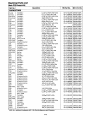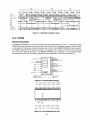
1
Tandy Service Manual
Navigating this CD
To view the contents of this CD use the bookmarks and Adobe Reader’s forward and back buttons to
browse through the pages. Alternatively use any table of contents or book index to look for specific
information and then use Adobe Reader’s page navigation controls in the status bar at the bottom of the
window to go to the relevant page.
Searching this CD
•
This CD is searchable using Adobe Acrobat Reader 4 or later. It is also FASTFIND enabled, giving
very fast searches of all files on the CD at once! The FASTFIND search enhancement only works with
Adobe Reader 6 or later. Use the Binoculars/Search icon in Adobe Reader or “Search” under the
Edit menu to initiate all searches.
•
For more information on advanced searching and other tips for the best search results click here
•
Generally 95% - 99% of the words can be searched. Where the original type was poor the words
may not be recognised for searching.
The technical advancements that allow this searching bring a wonderful finding aid but there is still no substitute for reading the book!
Copyright ©2006 Archive CD Books Australia Pty Ltd. All Rights Reserved
For more books on CD from Archive CD Books Australia, see the web site at www.archivecdbooks.com.au
Archive CD Books Australia exists to make reproductions of old books, documents and maps available on CD, and to co-operate with family and local
history societies, libraries, museums and record offices to digitise their collections in return for other benefits.
TANDY®
0
0
CUSTOM
MANUFACTURED
FORRADIOSHACK,
A DIVISION
OFTANDYCORPORATION
of
•
This is a blank page
CONTENTS
PART I. INTRODUCTION ........................................................................................ 1-1
System Overview ............................................................................................. 1-2
External View .................................................................................................... 1-2
Internal View ..................................................................................................... 1-5
Specifications ................................................................................................... 1-7
PART 11.DISASSEMBLY INSTRUCTIONS ............................................................. 2-1
Cases ................................................................................................................. 2-1
Keyboard and LCD PCBs ................................................................................. 2-1
Main PCB........................................................................................................... 2-2
PART III. MAINTENANCE ....................................................................................... 3-1
To clean the body and LCD display ................................................................ 3-1
PART IV. THEORY OF OPERATION .......................................................................
General ..............................................................................................................
Block Diagram ..................................................................................................
CPU ....................................................................................................................
Memory .............................................................................................................
I/O Map .............................................................................................................
Keyboard ..........................................................................................................
Cassette Interface Circuit ...............................................................................
Printer Interface Circuit ...................................................................................
Bar Code Reader Interface Circuit .................................................................
Buzzer Control Circuit ......................................................................................
System Bus .......................................................................................................
Clock Control Circuit .......................................................................................
Serial Interface Circuit .....................................................................................
LCD ....................................................................................................................
Power Supply Circuit .......................................................................................
4-1
4-1
4-2
4-3
4-3
4-5
4-6
4-7
4-8
4-9
4-10
4-11
4-12
4-14
4-21
4-24
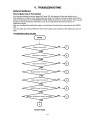
PART V. TROUBLESHOOTING .............................................................................. 5-1
General Guidance ............................................................................................ 5-1
Troubleshooting Guide .................................................................................... 5-1
Check List ......................................................................................................... 5-11
PART VI. EXPLODED VIEW/PARTS LIST ............................................................. 6-1
Electrical Parts List .......................................................................................... 6-2
Mechanical and Assembly Parts List ............................................................. 6-11
PART VII . SCHEMATIC DIAGRAMS/ PCB VIEWS ................................................ 7-1
Schematic Diagrams ........................................................................................ 7-1
PCB Views ......................................................................................................... 7-3
APPENDIX A/ INSTALLATION ............................................................................ A-1
Installation of Optional RAM and ROM .......................................................... A-1
APPENDIX B/ KEYBOARD LAYOUT, CONNECTOR PIN
ASSIGNMENTS AND CHARACTER CODE TABLE ....................... B-1
B-1. Keyboard Layout ..................................................................................... B-1
B-2. Connector Pin Assignments ................................................................... B-2
B-3. Character Code Table ............................................................................. B-7
APPENDIX C/ TECHNICAL INFORMATION .......................................................... C-1
C-1. 80C85A .................................................................................................... C-1
C-2. 81 C55 ....................................................................................................... C-7
C-3. 6402 ......................................................................................................... C-13
C-4. Basic Construction of LCD ..................................................................... C-19
io
List of Illustrations
FIGURE
NUMBER
DESCRIPTION
PAGE
NUMBER
1-1
1-2
1-3
1-4
1-5
2-1
2-2
2-3
4-1
4-2
4-3
4-4
4-5
4-6
4-7
4-8
4-9
4-10
4-11
4-12
4-13
4-14
4-15
4-16
4-17
4-18
4-19
4-20
4-21
4-22
4-23
4-24
4-25
6-1
7-1
7-2
7-3
7-4
7-5
Front View ................................................................................................................................ 1-2
Rear View ................................................................................................................................ 1-3
Bottom View ............................................................................................................................ 1-4
Main PCB (Bottom
....................................................................................................... 1-5
LCD PCB ................................................................................................................................. 1-6
Top Case Removal ................................................................................................................. 2-1
Keyboard and LCP PCBs Removal ....................................................................................... 2-1
Main PCB Removal ................................................................................................................. 2-4
Organization of Section IV ..................................................................................................... 4-1
System Block Diagram ........................................................................................................... 4-2
4-3
Functional Block Diagram of Bus Separation Circuit ...........................................................
Memory Map ........................................................................................................................... 4-3
Address Decoding and Bank Selection Circuit .................................................................... 4-4
I/O Address Decoding Circuit ................................................................................................ 4-5
"T" Key ............................................................................................... 4-6
Condition of Pressing
Cassette Interface Circuit ....................................................................................................... 4-7
Printer Interface Circuit .......................................................................................................... 4-8
Bar Code Reader Interface Circuit ........................................................................................ 4-9
Buzzer Control Circuit ............................................................................................................ 4-10
Time Set Sequence ofuPD1990AC ....................................................................................... 4-12
Time Read Sequence ofuPD1990AC ................................................................................... 4-13
4-14
Functional Block Diagram of the Serial Interface .................................................................
RS-232C/MODEM Selection Circuit ...................................................................................... 4-15
RS-232C Interface Circuit ...................................................................................................... 4-16
MODEM IC and Peripheral Circuit ......................................................................................... 4-17
Transmission Filter Circuit ..................................................................................................... 4-17
Reception Filter Circuit ........................................................................................................... 4-18
MODEM Adjustment ............................................................................................................... 4-19
MODEM Connector Interface Circuit .................................................................................... 4-20
HD44103 Internal Logic Diagram .......................................................................................... 4-21
4-22
HD44102 Internal Logic Diagram ..........................................................................................
LCD Waveform ........................................................................................................................ 4-23
Power Supply and Reset Circuit ............................................................................................ 4-25
Exploded View ........................................................................................................................ 6-1
7-1
Main PCB - Schematic Diagram ............................................................................................
LCD PCB - Schematic Diagram ............................................................................................ 7-2
Main PCB - Top View ............................................................................................................. 7-3
Main PCB - Bottom View ........................................................................................................ 7-4
LCD PCB - Top View .............................................................................................................. 7-5
A-1
B-1
B-2
B-3
B-4
B-5
B-6
B-7
C-1
C-2
C-3
C-4
C-5
Installation of RAM and ROM .................................................................................................
A-1
Keyboard Layout .................................................................................................................... B-1
System Bus Connector ........................................................................................................... B-2
RS-232C Connector ............................................................................................................... B-3
Printer Connector ................................................................................................................... B-4
Cassette Connector ................................................................................................................ B-5
MODEM Connector ................................................................................................................ B-5
Bar Code Reader Connector ................................................................................................. B-6
Functional Block Diagram ...................................................................................................... C-1
Pin Configuration of 80C85A ................................................................................................. C-1
Trap and RESET IN ................................................................................................................. C-5
80C85A Basic System Timing ............................................................................................... C-7
Functional Block Diagram ..................................................................................................... C-7
View)
iii
FIGURE
NUMBER
C-6
C-7
C-8
C-9
C-10
C-11
C-12
C-,13
C-14
C-15
C-16
C-17
DESCRIPTION
PAGE
NUM BER
Pin Configuration of 81 C55 .................................................................................................... C-7
Internal Register of 81 C55 ..................................................................................................... C-9
Programming the Command/Status
Register ......................................................................
C-10
Reading the C/S Register ....................................................................................................... C-11
Bit Assignments to the Timer Counter .................................................................................. C-11
Functional Block Diagram ...................................................................................................... C-13
Pin Configuration of 6402 ....................................................................................................... C-13
Receiver Timing ..................................................................................................................... C-16
Transmitter Operation ............................................................................................................ C-17
Start Bit Detection Timing ...................................................................................................... C-18
Construction of LCD Panel .................................................................................................... C-19
Operation Theory of LCD Panel ............................................................................................. C-20
List of Tables
TABLE
NUMBER
DESCRIPTION
PAGE
NUM BER
4-1
4-2
4-3
I/O MAP ................................................................................................................................... 4-5
Port Address of PIO ................................................................................................................ 4-5
System Bus Pin Assignments ................................................................................................ 4-11
B-1
B-2
B-3
C-1
C-2
C-3
C-4
C-5
C-6
System Bus Connector Pin Assignments ............................................................................. B-2
RS-233C Connector Pin Assignments.................................................................................. B-3
Printer Connector Pin Assignments ......................................................................................
B-4
Interrupt Priority, Restart Address and Sensitivity............................................................... C-4
80C85A Machine Cycle Chart ............................................................................................... C-6
80C85A Machine State Chart ................................................................................................
C-6
I/O Address of 81 C55 ............................................................................................................. C-9
Port Control Assignment........................................................................................................ C-10
Control Word Format .............................................................................................................. C-15
iv
I. INTRODUCTION
This manual is prepared for the Tandy 102 technicians working in field or in repair centers. Users of
this manual should be acquainted with the 80C85A microprocessor, the 81 C55 PIO and the 6402
UART. If you need more detailed information, refer to Appendix C in this manual.
This manual consists
of seven sections
and three appendices:
Section I
This section provides general information on the Tandy 102 such as specifications,
views and internal views.
external
Section II
This section describes the disassembly procedures.
Section III
This section describes the maintenance of the Tandy 102.
Section IV
This section describes the general theory of operation for the Tandy 102.
SectionV
This section describes how to troubleshoot the Tandy 102.
Section VI
This section provides an exploded view and parts list of the Tandy 102.
Section VII
This section provides the schematics,
Tandy 102.
PCB diagrams,
and silkscreen
views of the PCBs of the
Appendix A
This appendix provides instructions for installing the optional ROM and additional RAMs.
Appendix B
This appendix provides the character
assignments.
code table, keyboard layouts and connector
pin
Appendix C
This appendix provides the technical information of the 80C85A, 81 C55, 6402 and LCD.
System Overview
Tandy 102 portable computer is a low cost version of the Radio Shack TRS-80 Model 100 Portable
Computer. The Tandy 102 is fully compatible with the Model 100 in its software so that both system
users can take advantage of the large number of programs available.
The Tandy 102 has the following applications programs
TELCOM, ADDRSS, SCHEDL and TELCOM.
in the standard
ROM: BASIC, TEXT,
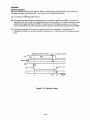
External View
1
Keyboard : Can be used like the standard typewriter. However, the Tandy 102 does have a few
speciatkeys.
(See Appendix B of this manual for more details.)
2
LCD Screen : The Tandy 102 display has eight lines that allow 40 characters
3
Power Switch : Move this switch towards the front to turn the power on. To conserve the
batteries, the Tandy 102 automatically turns the power off if you do not use it for 10 minutes in
default setting.
4
Low Battery Indicator : Before the Tandy 102 is operational
indicator will illuminate.
5
Display Adjustment Dial: This control adjusts the contrast of the LCD display relative to the
viewing angle.
6
External Power Adapter Connector: Connect the appropriate and of Radio Shack's AC Power
Supply (Catalog Number 26-3804, optional/extra) to this connector. Connect the other end of
the power supply to a standard AC wall-outlet or approved power strip.
1 Keyboard
1-1
N,
2 LCD Screen
batteries
on each line.
become exhausted,
this
4 Low Battery
Indicator
11-1
11-1
11-1
ZZ
6 External Power Adapter
Connector
5 Display Adjustment
Dial
3 Power Switch
Figure 1- 1. Front View
1-2
1
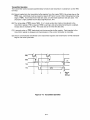
RESET Switch : If the Tandy 102 "locks up" (i.e., the display "freezes" and all keys seem to be
inoperative), press this button to return to the Main Menu (start-up). It is not likely that the
Tandy 102 will lock-up when you are using the built-in applications programs, however, it may
occur with customized programs.
2
RS-232C Connector: Attach a DB-25 cable (such as Radio Shack Catalog Number 26-1408) to
this connector when you need to receive or transmit serial information. When you
communicating directly with another TRS-80 computer, a Null MODEM Adapter (26-1496) is
required. An 8" Cable Extender (26-1497) may also be required.
3
SYSTEM BUS Connector : Connect this connector to the TRS-80 Disk/Video interface
(26-3806), using the system bus cable.
4
PRINTER Connctor: For hard-copy printouts of information, attach any Radio Shack parallel
printer to this connector, using an optional/extra printer cable.
5
Direct-Connect MODEM (PHONE) Connector: When communicating with another computer via
the Tandy 102's built-in MODEM, connect the round end of the optional/extra MODEM cable
to this connector.
6
CASSETTE Recorder Connector : To save or load information, on a cassette tape, connect the
cassette recorder here. An optional/extra cassette recorder (and cable) is required.
7
Bar Code Wand Connector : Attach the optional/extra
that special bar code reader software is required.
8
DIR/ACP Selector : This selector allows you to select either a direct or acoustic coupler
connection. If you are communicating with another computer over the phone lines via the
built-in, direct-connect MODEM, set this switch to the DIR position. If you are using the
optional/extra Model 100 Acoustic Coupler (26-3805), set this connector to the ACP position.
9
ANS/ ORIG Selector : If you are "originating" a phone call to another computer,
to ORIG. If another computer is calling your Tandy 102, set to ANS.
bar code wand to this connector.
Note
set this switch
5 Direct-Connect
MODEM (PHONE) Connector
6 CASSETTE Recorder
Connector
4 PRINTER Connector
3 SYSTEM BUS Connector
9 ANS/ORIG Selector
8 DIR/ACP Selector
7 Bar Code Wand
Connector
1 RESET Switch
2 RS-232C Connector
Figure 1-2. Rear View
1-3
1
MEMORY POWER Switch : This switch is used to prevent discharge of the internal
Nickel-Cadmium battery, which is used for RAM back-up. The Tandy 102 will operate only
when the power switch is set to ON. Set this switch to the OFF position when the Tandy 102 will
not be used for a long period of time. Note that the RAM will not be backed up when this switch
is set to the OFF position.
2
Optional ROM and RAM Compartment : An optional/extra
this compartment to enhance the Tandy 102 capabilities.
3
Battery Compartment : When not connected to an AC power source, the Tandy 102 gets its
power from four AA size batteries that must be installed in this compartment.
ROM and RAM can be inserted into
3 BATTERY Compartment
1 MEMORY POWER
Switch
2 OPTIONAL ROM and RAM
Compartment
X
X
11
O
O®
Figure 1-3. Bottom View
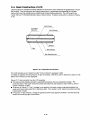
Internal View
The Tandy 102 consists of three printed circuit boards:
• LCD PCB
• Keyboard PCB
• Main PCB
d0V
ZI
ODO
T
6110f
%,V SIN
dl-
-4F
t
540
F
050
vw8£a
q S0
o 0C8
i-
£ o
SIN
608
_4
YD
r ssZ
V
980
m
T
1
T
-w
-
-IF
oqr
U
o
V90
m
N
V 1
6001
+F
iF
IMS
N
b
8010
9N0
c
L18
°
V
10
0180
I
L
9
L
aSSI
/
9•
Potentiometer VR1
for MODEM
Transmitting Level
SNV
E
r --
ZMS
L
£q0
iF
a
m
u T
co
1 SVI/500V9L
T
MODEM IC
Xtal for
MODEM IC
IANZ
2850
I- a
09DSs0
C90
-
L10
100
qqa
r0£W
f
F
a
°
¢
190
CON
RAM (8KBx3)
o
MC14412
801
RAM
Z
U
ID
Ex
CO
Battery for
Memory Back-up
RAM
--pp
I
HUM
m
01
m
!7
7
m
m
3-IFT
N
1
r
r'7
ci
=
°
r
2119
X
J
m
ROM
a
a
Xtal for
Main Clock
a
m
_
a
m
N
Z
m
v
f
o
N
£
>
I
4- 11
I
°
6119
09
1Z
4
9
CPU
(80C85A)
V
dd0 EMS
NO
Zx
PIO (81 C55)
8OC85
CIE
5815
IZN
UART (6402)
8IC55
9N3N
rt
e
z
IM6402
ZZ19
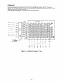
Figure 1-4. Main PCB (Bottom View)
1-5
_1131
L
0Z
Buzzer
J
q
LED
u
R12
R13
Cl
22
23
C2
RI1
R14
Mil
34
33
64
80
•
64
65
65
80.1
HD44102
MI0
u
HD
T
44102
M5
u
c%j
40
25
C20
41
40
4I
25
64
80
•
64
65
65
M9
44102
HD
M4
HD44102
80 • I
u
a
u
40
24
25
C19
41
40
4I
24
25
64
80
•
64
65
65
80.1
HD44102
M8
HD
44102
3
vgm
fm
<
m3
D
u
24
25
C18
41
40
C14
40
41-
24
25
•1
80
•
64
65
65
64
80
HD44102
M7
44102
HD
M2
N
u
24
25
C17
41
40
u
40
41N
24
25
80
64
65
65
64
80
HD44102
M6
44102
MI
u
24
25
C16
4140
40
41
24
25
44
M12
34
•
I
HD
33
10
II
u
RL6
12 .
v
23
22
u
a)
r
u
R,
y
Rs
r
C4
15
CIO
ro
Specifications
Main Components
Keyboard
Life of key switch
Number of keys
Function keys
Caps/NUM lock key
Other keys
LCD display
Display panel
Dot pitch
Dot size
Effective display area
Operation batteries
Batteries
Operation time
Memory protection battery (On Main PCB)
Battery
Back-up time
Recharge method
Charging current
LSIs
CPU
ROM
RAM
72 keys (8 x 9 key matrix)
3 millions keystrokes
0.5 million keystrokes
5 millions keystrokes
240 x 64 full-dot matrix
duty
bias
0.8 x 0.8 mm
0.73x0.73 mm
191.2(W) X 50.4(D) mm
1/32
1/6.66
Four type AA
Alkaline-manganese
batteries
5 days (Typ.) - 4 hours per day
20 days (Typ.) - 1 hour per day
(Note: without I/O units at normal temparature)
Rechargeable battery (50mAh/3.6V)
More than 20 days-16 KB RAM
More than 10 days-32 KB RAM
Trickle charge by AC adapter
operation batteries
1.2 mA (Typ.)
80C85A
Code and pin compatible with 8085
Maximum 64 KB
Standard 32 KB
Optional 32 KB
Maximum 32 KB
Standard 24 KB
Optional 8 KB
Power consumption
65 mA (Typ.)
Dimensions
8-1/2"
11-3/4" (W) X
(D) X 1-1 /2" (H)
300 (W) X 215 (D) X 38.5 (H) mm
Weight
3 lbs. 2 oz. (with batteries)
1.4 kg
I/O Interface
RS-232C
Conforms to EIAstandard signal
TXR (Transmit Data)
RXR (Receive Data)
RTS (Request to Send)
CTS (Clear to Send)
DSR (Data Set Ready)
DTR (Data Terminal Ready)
Communications protocol
Word length
Parity
Stop bit length
Baud rate
Maximum transmission distance
Maximum driver output voltage
Minimum driver output voltage
Maximun receiver input voltage
Minimum receiver input vltage
MODEMICoupler
Conforms to BELL 103 Standard
Data length
Parity
Stop bit length
Baud rate
Full duplex
Transmit output level
Receive sensitivity
Other functions
Printer interface
Conforms to Centronics interface standards
Handshake signals
6, 7, or 8 bits
NONE, EVEN or ODD
1 or 2 bits
75, 110, 300, 600, 1200, 2400,
4800, 9600 or 19200 BPS
5 meters
± 5 volts
± 3.5 volts
± 18 volts
± 3 volts
6, 7 or 8 bits
NONE, EVEN or ODD
1 or 2 bits
300 BPS
Answer mode/originate mode switchable
15 dBm ± 2dBm
-30 dBm
Hang-up function
Auto pulse dialing function
10/20 PPS
STROBE, BUSY, BUSY
rf
Audio cassette inte ace
Data rate
Input level
Output level
1500 BPS
(Mark 2400 Hz, Space 1200 Hz)
0.8 to 5 volts (Peak to peak)
580 mV ± 10%
rf
Bar code reader inte ace
Input level
3.5 volts (Min.)-High
1.5 volts (Max.)-low
II. DISASSEMBLY INSTRUCTIONS
Cases
1. Disconnect the cables from the unit.
Taking care not to scratch the LCD screen and key tops, turn the unit over and remove 4 screws
A from the upper and lower cases.
2. Remove the upper case.
Therefore, the upper and lower cases are secured by snaps. Pull up the front of the upper case
first, as shown below.
Also, do not apply too much force when pulling it.
A
Figure 2-1. Top Case Removal
Keyboard and LCD PCBs
1.
2.
3.
4.
V
Disconnect the flat cable from the connector on the keyboard PCB.
Remove the keyboard PCB.
Disconnect the flat cable from the connector on the LCD PCB.
Remove the LCD PCB.
V1
I
1
e
C5
Figure 2-2. Keyboard and LCD PCBs Removal
2-1
Main PCB
1. Remove the insulator board.
2. Remove 2 screws B securing the main PCB and bottom case.
3. Remove the main PCB.
0
C)
B
U
CD
U
Figure 2-3. Main PCB Removal
III. MAINTENANCE
To Clean the Body and LCD Display
1. To avoid operational trouble, always keep the Tandy 102 clean.
2. Clean the body and the LCD screen using a soft, dry, lint-free cloth.
3. For tough stains, clean the body or the LCD screen with benzol.
Caution: Do not use any solvents other than benzol.
This is a blank page
IV. THEORY OF OPERATION
General
Figure 4-1 shows how this section is organized
and highlights significant areas.
Theory of
Operation
Block
Diagram
General
CPU
I
1
Memory
I/O Map
Address
Decoding and
Bank Selection
Circuit
Cassette
Inte ace
Circuit
rf
Keyboard
Printer
Interface
Circuit
Bar Code
Reader Interface
Circuit
Buzzer Control
Circuit
11
Signal from PB5
of PIO
Read Circuit
Remote Circuit
System Bus
Clock Control
Circuit
Timer Set
Sequence
Using PIO Times
Output
rf
Serial Inte ace
Circuit
MODEM
Selection Circuit
fRS-232C/
RS-232C
Interface Circuit
MODEM IC
Timer Read
Sequence
LCD Common
Driver
LCD Segment
Driver
LCD Waveform
Transmission
Filter Circuit
Reception Filter
Circuit
MODEM
Transmitting
Level
Adjustment
y
MODEM
Connector
Circuit
Figure 4-1. Organization of Section IV
4-1
Power Supply
and Auto- Power
ON/OFF Circuit
LCD
I
1
DC/DC
Converter
Low Power
Detection Circuit
Reset Circuit
Block Diagram
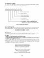
The Tandy 102 has three principal LSIs.
• 8OC85A CPU
This is the Central Processing Unit which controls all functions.
• 81 C55 PIO
This is the Parallel Input/Output interface controller which controls the printer interface,
keyboard, buzzer, clock and LCD interface.
• 6402 UART
This is the Universal Asynchronous Receiver Transmitter which controls the serial interface
(RS-232C or MODEM).
The input/output for a cassette recorder and the input of the BCR are controlled by CPU directly
through its SOD, SID and RST5.5 terminals.
ROM and RAMs are connected to the system bus. ROM is available only for alternative selection
from Standard or Option.
CPU
8OC85
CASSETTE
INTERFACE
PC
FKEYBOARD
B
I
KEYBOARD
ROM
32KB
STANDARD
RAM
8KB
i
PRINTER
PIO
81 C55
RAM
8KB
i
RAM
8KB
INTERFACE
LCD
CONTROL
LCD
I
CLOCK
yPD1990AC
LCD P
I
I
I
RAM
8KB
UA RT
OPTION
6402
ROM
32KB
OPTION
SYSTEM BUS
SOCKET
Figure 4-2. System Block Diagram
RS-232C
INTERFACE
CPU
The CPU is an 80C85A that runs at a clock speed of 2.4576 MHz. It is an 8-bit, parallel Central
Processing Unit using C-MOS technology.- The instruction set is fully compatible with the 8085A
microprocessor. The 80C85A uses a multiplexed data bus. The CPU bus is divided into two
sections- the 8-bit address bus named the A8-A1 5, and the 8-bit address and data bus named the
ADO-AD7. The address bus signals are separated at M1, using the ALE* (Address Latch Enable)
signal.
M20.M21
A8-415
",
AS-A15
CPU
A0-A7
M2
ADOAD7
ADO-AD7
M20
RD
RDA
ALEX
ALE
M20
Figure 4-3. Functional Block Diagram of Bus Separation Circuit
Memory
The memory of the Tandy 102 consists of a 32 KB standard ROM, three 8 KB C-MOS static RAMs
and a 32 KB optional ROM.
The standard RAMs equipped in the Tandy 102 are M9, M8 and M7. By installing M6, memory
capacity can be increased to 32 KB. The ROM used in the Tandy 102 is a 32 KB (256K bits)
memory.
It is operated only by a +5V power source with an access time of 600 nsec (Max.).
The BASIC program and BIOS program which operate the LCD, printer etc. are stored in the
standard ROM.
An optional ROM can be installed onto the special IC socket by removing the ROM cover on the
bottom case of the Tandy 102. Various types of application programs are stored in the optional
ROM.
0000H
OPTION
STANDARD
ROM
BAN K
(
7FFFH
8000H
9FFFH
AOOOH
BFFFH
COOOH
32KByte) SELECTION
(32K Byte)
--
OPTION
RAM
I
( 8K B te)
ST
A
RAM
3
B
(SK to)
STANDARD
RAM
2
DFFFH
E000H
FFFFH
STANDARD
RAM
I
K B t
Figure 4-4. Memory Map
4-3
-
-
-
- -STANDARD
Address Decoding and Bank Selection Circuit
Although four 8 KB static RAMs and two masked ROMs can be installed in the Tandy 102, six
chip-select signals are required.
Because the RAMs are positioned from 8000H to FFFFH, and ROMs are positioned from OOOOHto
7FFFH, address signal Al 5 selects the ROMs or RAMs at M5. At another section of M15, address
signals Al 4 and A13 select each RAM corresponding to the memory map. The ROMs (both
standard and optional) installed in the Tandy 102 are the 32 KB 1-chip type. As shown in the
memory map, the address space is positioned from OOOOHto 7FFFH.
The chip select signals are generated by the A15 and STROM signals. The ADO is latched at M14
by the WR signal and Y6 signal, and then the STROM signal is generated.
The standard ROM is selected by the low level STROM signal and the optional ROM is selected by
the high level STROM signal.
M5
0000-7FFFH
TO4
Standard ROM
0000-7FFFH
Y1
Option
5
ROM
M5
Y2 6
4
ADO
Y6
WR*
RDXE
10
9
5
4
8
26
M14
9 C
6
17
D
Q 2
STROM
2 A
Y3
3
8
8000-9FFFH
1
85
37
7
TO12
11 10
13
9
37
Option
RAM
A000-BFFFH
G
Y1 11
12 0 11 A0#
RAM # 3
0000-DFFFH
Y2 10
RAM
#2
A15
A13
A14
14 A
13
E000-FFFFH
Y3
8
Figure 4-5. Address Decoding and Bank Selection Circuit
9
RAM
#1
I/O MAP
As shown in the figure below, the I/O address decoding circuit, consisting of M16, decodes address
signals A12 to Al 5 and generates I/O selection signals YO to Y7.
The application of the selection signals (YOto Y7) for the I/O devices are shown in Table 4-1.
Table 4-2 shows the port address of the PIO.
16
15
6
10f
G1
YO
M16
1
3
M17
A15
2
4
13
G 2A
12
5 G2B
40H138
3
A 14
2
A13
A12
14
1I
NC
Y2
Y3
Y4
10
Y5
C
9
B
7
A
Y6
Y7
8
Figure 4-6. I/O Address Decoding Circuit
Address
Signal
Active Level
Application
Free area for an optional unit and other select signals of various circuits made by user.
OOH- 7FH
-
80 - 8FH
YO
L
Device-select signal for optional I/O controller unit.
90H - 9FH
Y2
L
Enable signal for relay RY3 in MODEM connector
interface circuit.
BOH - BFH
Y3
L
PIO (81 C55) chip-select signal.
COH - CFH
Y4
L
Enable signal for data input/output
DOH- DFH
Y5
L
Enable signal to set various modes and read port
of UART.
EOH- EFH
Y6
L
Enable signal for STROM and REMOTE, and input
data from keyboard.
Strobe signal for printer and clock.
FOH- FFH
Y7
L
Enable signal for LCD driver LSI.
port of UART.
Table 4-1. I/O Map
Port or Register
Address
BOH or B8H
Command/status register (internal)
B1 H or B9H
Port A
82H or BAH
Port B
B3H or BBH
Port C
B4H or BCH
Timer register lower byte
B5H or BDH
Timer register upper byte
B6H, B7H, B8H and B9H
Not used
Table 4-2. Port Address of PIO
4-5
Keyboard
Key strobe signals are emitted from the PAO to PA7 and PBO terminals of the PIO. The return
signals from the keyboard pass through the bus buffers (Ml 5 and M3) and send to the CPU. The I/O
address of the return signals is EOH-EFH.
The condition of pressing the "T" key is shown in the figure below.
33KX8
AD7
AD
IS
AD
5
AD4
M15
M3
AD3
A02
AD 1
ADO
KEYBOARD
KR7
17
KR6
16
KR5
15
KR4 - -
--
-
14 -
KR3
43
KR2
12
KR1
11
KRO
110
L
K
M
J
U
N
H
Y
UNIT
>
V
82PXB
a
4
PRI
T
f7
A
-e
EL
f6
B
S
t
P
+
ESC f4
E
co
DE
D I
E
]
4
TAB
f3
x
s
W
P
n4
DEL
f2
A
2
I
0
Q
13
4
/
5
PH
RL
SFA f1
(
6
PS
f5
C
Z
WRE
ME
f8
SHI
FT
CE
7
8
9
CD
0
0
D
.
N
D
W
D
A
Figure 4-7. Condition of Pressing "T" Key
D
O
D
W
D
-
SHI
FT
J
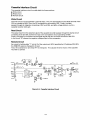
Cassette Interface Circuit
The cassette interface circuit is subdivided into three sections:
• Write circuit
• Read circuit
• Remote circuit
Write Circuit
The write circuit is accomplished in several steps. First, the serial data from the SOD terminal of the
CPU is inverted by M34. Then, the DC component is removed by C63. Finally, the data
passes through an integrator consisting of R51 and C64, and after voltage division, out to a
cassette recorder AUX jack.
Read Circuit
The signal input from the earphone jack of the cassette recorder passes through the clamp circuit
consisting of D5 and D6, and then is input to the comparator circuit consisting of M30.
Finally, the signal is converted into the digital signal and sent to the SID terminal of the CPU.
In this circuit, D7 clamps the negative voltage output of the comparator.
RemoteCircuit
As a result of writing data "1" into bit 3 of the output port (Ml 4) specified by I/O address EOH-EFH,
the REMOTE signal is changed to H level.
Then, T6 is switched on and relay RY1 is energized. This causes the drive motor of the cassette
recorder to operate.
0
0
Y.
It
t0
,n
U
IS) M
E-TXC
C
R54
5
R51
D:
C63
M
2
12K
7
2 .2K 0.1p
VDD
4584
RXC
4
8
RY 1
r'---1
REMi
REM2
GND
3
2
5
1
I
21
6
L. _
R52
10012
1K
08
(
I p'
---
R95
)Xp
VR
1 4
I I
6
GND
pj
1
j
1j
SOD
3
n
10
M
N
.j
M
0
ti
0
N
N
M30
+
11
R72
14
M
5
33K
6 SID
L
12
Y
VEE
D
Y
a)
4584
4
13
x
,
C
VDD
t_
so
0
N
R132150K
R50
REMOTE
3.3K
T6
Figure 4-8. Cassette Interface Circuit
Printer Interface Circuit
The printer interface circuit conforms to Centronics standards. As shown in Figure 4-9, the BUSY
signal from the printer is read from the PC2 of the PIO. If the condition is not busy (PC2 = L), the
8-bit parallel data (PAO - PA7) is sent to the printer. Then, by writing data "1 " into bit 1 of the output
port specified by I/O address EOH-EFH,the PSTB signal is sent to the printer.
As soon as the printer receives this PSTB signal, the BUSY signal is changed to H indicating that
the printer is busy. The CPU then waits for a while until this BUSY signal becomes L. The printer
prints the one character corresponding with the 8-bit parallel data. After completion of the one
character printing, the printer sets the BUSY signal to L. Then, the CPU sends the next 8-bit parallel
data. If the printer is in ONLINE condition, the BUSY signal is H and sent to the CPU, passing
through the PC1 of the PIO. However, when in the OFFLINE condition, the BUSY signal is L and
transmission of print data to the printer is inhibited by the CPU.
AD1 5 DM14 Q 6
PSTB
1
0
3
A
PA
2
3
6
8
PA3
32
9
PAO
PA 1
10
Y6
WR
26
8
9
PA4
PA
5
PA
6
PA
7
BUSY
10
P03
10 GND
PD4
12
#
10
STROBE
GND
PDO
GND
PD1
GND
PD2
GND
16
1
GND
PD5
GND
PD6
GND
PD7
U
W
GND
GND
0:
W
i^
BUSY
GND
0_
VDD
20
PAO-7
21
5-
PC2
R 6433K
STROBE
R6833K
PCI
C38 100P
0.5
A(Min)
Ill
Figure 4-9. Printer Interface Circuit
24
0:
0
NC
GND
BUSY
Z
z
0
U
Z_
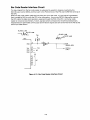
Bar Code Reader Interface Circuit
The input signal from the bar code reader is subjected to waveform shaping, inverted by the
Schmitt-type inverter (M34), and then sent to the PC3 terminal of the PIO and the RST5.5 terminal of
the CPU.
When the bar code reader reads the first white part of the bar code, a L level signal is generated,
then inverted by M34 to notify the CPU of an interruption. As soon as RST5.5 interruption occurs,
the CPU starts the data input operation, passing through the PC3 of the PIO. As the bar code
reader is moved across the bars, H and L signals (which correspond to the white and black bars,
respectively) are generated continuously and inversion signals are sent to the PC3 of the PIO as the
serial input data stream.
BLACK
LINE
WHITE
LINE
BLACK LINE
WHITE LINE
VDD
CNI
Y
M
M
0
ti
Q:
I
RXD
13
2
M
12
BCR
( 8IC55-PC3)
9
VDD
GND
GND
5
Voo
NC
7
1
3
6
NC
4
8
Figure 4-10. Bar Code Reader Interface Circuit
RST5.5
(CPU)
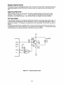
BuzzerControlCircuit
There are two ways to operate the buzzer. One is to sound the buzzer with the specified frequency
by emitting signals from the PB5 of the PIO and the other, by using the timer output signal of the
PIO.
Signal from PB5 of PIO
When the PB2 of the PIO is H, the buzzer sounds by repeated switching of the buzzer driving
transistor. This is caused by H, L, H, L ... output signals from the PB5 synchronizing with the
frequency for sounding the buzzer. This method is used for the BEEP command in BASIC.
PIO Timer Output
In this method, the buzzer is sounded by setting the PIO timer in the square wave output mode. To
write the value corresponding to the sound frequency, the CPU assigns B4H, B5H, BCH or BDH to
the I/O port address. This frequency is assigned by the first parameter of the SOUND command in
BASIC.
If the above procedures are completed, the TO terminal of the PIO outputs the square waves, and
the P62 of the PIO controls the length of the sound whenever the PB5 is "L". How long the sound is
heard depends on the second parameter of SOUND command in BASIC.
VDD
PB5
P10
PB2
TO
T1
2SA
1162
VDD
M25
31
R61
33K
12
6
13 M26
R2
33K
oa
BUZZER
R4
R3 33K
33K
R113
3.3K
11
VEE
Figure 4-11. Buzzer Control Circuit
System Bus
In order to expand the use of external devices, a 40-pin system bus connector is mounted on the
back panel of the Tandy 102.
As shown in the Table 4-3, the address bus, data bus and control bus can be connected to the
external devices passing through the drivers or receivers, thus making system expansion easy.
Pin No.
1
2
3
4
5
6
7
8
9
10
11
12
13
14
15
16
17
18
19
20
21
22
23
24
25
26
27
28
29
30
31
32
33
34
35
36
37
38
39
40
Signal
VDD
VDD
GND
GND
ADO
AD1
AD2
AD3
AD4
AD5
AD6
AD7
A8
A9
A10
All
A12
A13
A14
A15
GND
GND
RD*
WR*
10/M *
SO
ALE*
Si
CLK
YO
A*
RESET*
INTR
INTA
GND
GND
RAM RST
NC
NC
NC
Description
+5V power supply
+5V power supply
Ground
Ground
Address and data signal bit 0
Address and data signal bit 1
Address and data signal bit 2
Address and data signal bit 3
Address and data signal bit 4
Address and data signal bit 5
Address and data signal bit 6
Address and data signal bit 7
Address signal bit 8
Address signal bit 9
Address signal bit 10
Address signal bit 11
Address signal bit 12
Address signal bit 13
Address signal bit 14
Address signal bit 15
Ground
Ground
Read enable signal
Write enable signal
I/O or memory select signal
Status 0 signal
Address latch enable signal
Status 1 signal
Clock signal
I/O controller select signal
I/O or memory access enable signal
Reset signal
Interrupt request signal
Interrupt acknowledge signal
Ground
Ground
RAM enable signal
No connection
No connection
No connection
Table 4-3. System Bus Pin Assignments
Clock ControlCircuit
A clock LSI (4PD1990AC) is used in the clock control circuit so that the time and date information
can be set and read by the CPU.
As shown in Figures 4-12 to 4-13, when the Tandy 102 is in the operable condition (RESET is H),
commands and data can be input and output to,uPD1990AC from the CPU at will. In addition,
because back-up power supply VB is applied to theuPD1990AC, the clock functions even when the
Tandy 102 power switch is OFF.
The DATA IN, CLOCK and C0-C2 terminals ofpPD1990AC are connected to the PAO-PA4 terminals
of the PIO. The DATA OUT terminal is connected to the PCOterminal of the PIO. The STB signal is
provided from bit 2 of the output port made by M14.
The TP terminal of the ,uPD1990AC is connected to the RST7.5 terminal of the CPU. Square waves
are output from the TP (4 ms cycle), and one key scan occurs every 4 ms because of the RST7.5
interruption to the CPU.
Time Set Sequence
The CPU set 4uPD1990ACto the register shift mode with the "100" pattern of the C0-C2 and the
strobe signal which is generated by the AD2, Y6 and WR* signals passing through M14.
Then, the CPU sends the data of time and date information to the DATA IN terminal of,uPD1990AC
with timing clock PA3.
Finally, the CPU sets APD1990AC to the time set mode with the "010" pattern of the C0-C2 and the
strobe signal.
120
_FL
010
0 10
120
AD
2
40H175
M14
40H 175
M14
CK CLR
Y6 -
M26
WR* -
0
--
CK CLR
Y6
1
J
MZ
WR*--
RESET
RESET
Y
MU
a. rna
a.
MU
Ma
i-
gr
VB
14 OE
C19
0.047J1
25V
TP
CS
STB 12
OUT
JJPDI990AC M18
xi
13
7
CO
C1
1
O
a
a
C2 DATAINCLK
i
N
V
M
a
a
a
cis 20P
c3C17
20P
11
32.768 kHz
VB
14 OE O TT
xic3
13
7
CO
C1
1
t
Cu
O
a
C2 DATAINCLK
1
1
a
Figure 4-12. Time Set Sequence of ,uPD1990AC
a
cis
CS STB 12
JJPD1990AC M18
O.047;,
25V
TP
20P
C1 20P
32.768 kHz
Time Read Sequence
pPD1
990AC
The CPU sets the
to the time read mode with the "110" pattern of the C0-C2 and strobe
signal.
Then the CPU sets the register shift mode with the "100" pattern of the C0-C2, and reads the data of
time and date information from the DATA OUT terminal. At the same time, the CPU sends the PA3
signal passing through the PIO for the read timing clock.
Y6 WR*--
Y6 -
M26
M2
WR*-RESET
RESET
-Y y
M O
M U
MCL
F-
VB
DATA
TP
T
14 OE D
C19
0.047)J
25V
CS
JJPDI990AC M
CO
Cl
STB 12
18 13x1O
C2 DATAINCLK
VB
C1820P
I
C17 20P
32.768 kHz
14 OE
C19
0.047)j
25V
DATA TP
OUT
CS
JJPD1990ACM18
x1p
13
7
CO
C1
C2 DATAINCLK
O
-
N
M
a
a
a.
a
Figure 4-13. Time Read Sequence of ,uPD1990AC
C18
STB 12
11
20P
C1720P
32.768 kHz
Serial Interface Circuit
The serial interface circuit supports asynchronous data transmission/reception.
The heart of this
circuit is the 6402 (UART). It performs the job of converting the parallel byte data from the CPU to a
serial data stream including start, stop and parity bits.
For a more detailed description of how this IC performs these functions, refer to Appendix C of this
manual.
Figure 4-14 shows the functional block diagram of the serial interface circuit. In this figure, the TO
signal, basic timing clock for the UART, defines the transmission/reception
baud rate.
To transmit and receive the serial data from external devices, the RS232C signal selects either
MODEM or RS-232C interface. During the MODEM operation, the MODE signal switches either the
originate mode or answer mode for the MODEM IC.
The serial interface circuit is subdivided into the following circuits:
• RS-232C/MODEM Selection Circuit
• RS-232C Interface Circuit
• MODEM IC
• Transmission Filter Circuit
• Reception Filter Circuit
• MODEM Connector Circuit
RS232C
DT-R
PI0
CPU
R
M
D R
CN6
M38
M13
M
TS
U
N
M24
:Y °
Er
CL/AS
M33
RXCAR
OORIRIrGo
h ANS
RY2
RXM
TRO
RRI
TXM
M31
RY3
L
DIR
CN4
TXMD
ACP
TL
MODEM
UART
OE.FE.PE.
DIR
CP/TL
MODE
ACP
M23
M4
M26
Figure 4- 14. Functional Block Diagram of the Serial Interface
TXM
RXM
RP
RS-232C /MODEM Selection Circuit
The RS232C signal (PB3 terminal of the PIO) determines whether the serial port is to be used for
RS-232C or for MODEM. When the RS232C signal is H, the serial port is used for MODEM.
The reception signals, including the control signals, are demultiplexed at M33.
During the RS-232C mode, the CD (Carrier Detect) signal is not used. To make this condition, pin
14 of M33 is connected to the ground.
During the MODEM mode, the CL/AS signal is used as the sensing signal for the ORG/ANS switch,
and CP/TL signal is used as the sensing signal for the ACP/DIR switch. In order to detect the
carrier signal from the telephone line, the CD signal is connected to the RXCAR terminal of the
MODEM IC.
r-------I
RRI
CTS
DSR
CD
1A 2
/2A 11
1
0
S =
3
////
//4A I
4 1Y w 1B 3
6
T
2Y
2B
9
3B 10
12 4Y
4B 13
1A 2
RXR
CTSR
DSRR
Z;
3y
RRI
CTS
DSR
CD
9
10
r-
19
.8
38
1011
M
13
RXM
WAS
CP/TL
RXCAR
9
8
10 M13
TXR
M13
2A 5
Ao
3A
S =3
14
to 4A
4 1Y' '+ 1B
7 Y
2B
9 3Y '
1
1
12 4Y
9
8
RTSR
M38
10
12
TXM(M31)
TRO
RTS
3
2
2
M38
3
38
1
3
A
MODEM
RS-232C
W
N
n
Figure 4-15. RS-232C/ MODEM Selection Circuit
RTSM
RS-232C Interface Circuit
In the RS-232C transmission circuit, after the DC component is removed from the signals by the
coupling capacitors, the signals are leveled to ±5V signals by the inverters connected in
parallel, and then are output as RS-232C transmission signals.
In the RS-232C reception circuit, the DSRR, CTSR, and RXR signals from the external RS-232C line
are subjected to waveform shaping and inverted by M24, and then converted to +5V or ground level
signals by the diodes.
4584
i2 _ -13
(0
Z
0
GND
---
35
1
2
0
33 n 110
RXR
GND
4
18
5
3
R96
18K
R8
6.2K
R9
18K
R9218K
R77
33K
R80
33K
13 2
9
R76
C720.039 )L
24
12
8
1
I
R137i00K
D9
R138 1OOK
D10
11 24
I
L ---------
M13
(pin8)
33K
C 73
O.O39.
VEE
R87 6.2K
7
1OOK
o.039)1
5
330n]
6.2K
R7
C71
M 38 (pin 13)
R81 1OOK R79 33K
35 9
35
R89
33K
3
35
R99
CTSR
35
20
6
R74
11
I
4
R9433
DSRR
R751 0K R73 33K
1
35
R9
DTRR
0
1
2
TXR
RTSR
VDD
-1
R139 1ooK
10
I
D8
VEE
Figure 4-16. RS-232C Interface Circuit
R65 DTR
M 25 (pin
35)
33K VDD
M 33 (pin11 )
M33
M 33
(pin5)
(pin 2)
MODEM IC
The Tandy 102 employs the IC MC14412 as a MODEM control device. This IC modulates/
demodulates data to be transmitted/received
in accordance with frequencies suitable for originate
or answer mode respectively.
The RXRATE and TYPE terminals of the MC14412 (M31) are pulled up to VDD. The baud rate is set
to 300 bps and the U.S.Standard is selected. Since the ECHO and SELFTEST terminals are not
needed, they are connected to ground.
The Q output (EN signal) of the M36 selected by bit 1 of the Y2 port is input to the ENABLE terminal
when the MODEM mode is selected.
In addition, the signal detected by the ORG/ANS switch is input to the MODE terminal, and it
switches between the ORIGINATE mode or ANSWER mode.
R47 15M
VDD
0
MHz
XTAL1
VDD
RXRATE
TTLD
TO TRANSMISSION
FILTER CIRCUIT
TYPE
16
6
R46
33K
15
14
TXCAR
13
ECHO
2
SLFTEST
B
Vss
FROM RECEPTION
FILTER CIRCUIT
9
M13
RXCAR
ENABLE
MODE
RXM
TXM
RESET
WR*
TT C)02
7H IOOP
C
0
12
Y2
10
VDO
D
AD)
ORIG
10
7
ANS
RS-232C/MODEM
1
5
J SELECTION
R12
1K
CIRCUIT
RESET
MB
(MC14412)
Figure 4- 17. MODEM IC and Peripheral Circuit
Transmission Filter Circuit
The DC component of the carrier output from the TXCAR terminal is removed by C61. The signal
level is adjusted by the potentiometer VR2. The signal then passes through the transmission
band-pass filter and is sent to the telephone line or the acoustic coupler.
The transmission filter circuit is composed of an active filter (consisting of an operation amplifier)
and the intermediate frequency of the active filter is 1170 Hz for the originate mode, and 2125 Hz
for the answer mode. They are changed by switching T4 ON or OFF.
C60
M31
MC14412
3500P
C61 4700P
R44 242K
R63620n
DIR
2
1
9
TXCAR
VR2
50K
M30
OTI
+3
VDD
ACP
CN4
Pin-5
C59
3300P R43 10K
R45
7.97K
R32 22a
R42
2.3K
CL AS
TXMC
T4
R33
10K
C103 2 20,u
ANS
ORIG
R11
1K
Figure 4- 18. Transmission Filter Circuit
4-17
Reception Filter Circuit
As shown in Figure 4-19, the reception input signal is amplified when passing through coupling
capacitor (C40), and amplified again as it passes through the 3-stage band-pass filter (composed of
an active filter). The signal then passes through the comparator, and after being changed to a
square wave, is input at the RXCAR terminal of the MC14412. Also, to check a carrier signal, this
signal is input to the demultiplexer M33.
The intermediate frequencies of the 3-stage active filter are shown below. The switching of
intermediate frequency for the originate and answer mode is accomplished by switching T2, T3 and
T5 ON or OFF according to the ORG/ANS switch position, thus changing the input resistance of the
filters.
1st stage
Intermediate
(
Frequercy
2nd stage
3rd stage
Originate Mode 980Hz
1150Hz
1330Hz
Answer
2120Hz
2290Hz
Mode 1940Hz
(d8)
G
(d8)
(dB)
0
GG
I
f
i
I
f(HZ)
f (Hz)
;
f(HZ)
C46
4700P
C109 68P
C41 4700P
C43 4700P
1118
590K
1129
28OKF
470K
DIR
C40
R19
0T7
0047y
ACP
tSK
13
RXM->•0
1-4
Pin-4
+
732K
14
M29
12
, R35 10K
>n
0z
n
n =
y
VDD
4
11
9
1117
Q
332K
R15
M29
g
+
R
v
7
M29
Y
Ma
„{
e
+
f
c
cop
422K
M29
*
n
5
R30
of
3
2 2K
R31
'
9
M30
8
10
+
TL064
0
I
I
16
r----
7
M30
+
+
R26
T2
R23
T3
10K
10K
10K
C2712
C2712
C2712
180K
TS
ORIG
ANS
R12
1K
Figure 4-19. Reception Filter Circuit
4-18
D29
IS2076
R37
R14
R41
93CAR
111311
10K
5
VEE
1 VDD
C
00
1110
11160
f00K
Modem Transmitting Level Adjustment
1. Set the DIR/ACPswitch to the DIR position.
2. Connect a 600-ohm dummy load between pin-3 (RXMD) and pin-7 (TXMD) of the MODEM
connector (CN4).
3. Connect an AC voltmeter across the above dummy load.
4. Set up the Tandy 102 in BASIC mode and enter the following command to generates the carrier
signal:
OUT 178 ,47 [ENTER]
OUT 168 ,02 [ENTER]
5. Adjust VR2 so as to read -14 to -17 dBm on the AC voltmeter for both ANS and ORIG modes.
600n
0
0
0
VR2
o
C
o ooooo0000
ooooo000000
0 0 0000 000
O
Figure 4-20. MODEM Adjustment
0
MODEM Connector Interface Circuit
When the acoustic coupler is used, the transmission and reception signals are directly connected
to the connector (TXM, RXM). When the MODEM cable is used, they are connected to the
secondary side of the driver transformer. The primary side of this transformer is connected to the
telephone line via the connector (TXMD, RXMD).
The ACP/DIR switch is used in the MODEM mode, relay RY3 separates the telephone receiver
audio signal (TL) to prevent interference. RY2, another relay, separates the MODEM circuit and the
telephone at the conclusion of use in the MODEM mode and is also used as an automatic dialer for
the pulse-type telephone line.
D16 VDD
VDD
MODEM
RTSM
T7
R49
RY2
I
6R48
3.3K
6
C103
220j
2
CN4
GND
R32
F rom
Transmission
Filter Circuit
TXM
22n
4
ACP
DIR
620n
OT1
T
1
R63
Iv
TL
TX MD
D24
ACP
DIR
RXM
N
""
D18
R171
I
RXMD
To Reception
Filter
Circuit
ADO
D
M36p
C
RP
DI D2 R21
T24
R134
3.3K
VDD
RY3
D21
R135
68K
Y2
WR*
C102
Figure 4-21. MODEM Connector Interface Circuit
LCD
The LCD used in the Tandy 102 is composed of electrodes in a matrixarrangement (64 common
signals and 480 segment signals ) This part is subdivided into the following three sections:
• LCD Common Driver
• LCD Segment Driver
• LCD Waveform
For a more detailed description
Appendix C of this manual.
of how the LCD operates
and its basic construction,
refer to
LCD Common Driver (HD44103)
The Tandy 102 uses two common driver ICs: M11 and M12. M11 controls the upper half of the LCD
screen and M12 controls the lower half of the LCD screen. M11 and M12 are cascade connected,
and a 1/32-duty backscan signal is made. By using C5 and R10 connected to the C and R terminals
of M11, a timing signal is generated, which controls M12. M11 can be considered to be the master
IC and M12 the slave.
The FRM signal defines the periodic frequency of one-screen display, and determines 70 Hz for the
Tandy 102.
The MB signal is used for changing the driver signal to AC, because the continuous application of
DC to the LCD would shorten the LCD element life.
The CL1 signal is used for the shift clock of the internal shift register.
The 01 and 02 signals are the clock signals for the HD44102 RAM operation.
2OLines
LCD
Driver
20Lines
DL
20Steps 8i-Directional
Shift Register
Logic
Logic
DR
CL
SHL
FCS
FRM
-f--0
M
+--o
Rf
Cf
.
OSC
Divider
CLK
(01,02)
VDD
-00--0
V1
Logic
Divider
Logic
FrameFrequency
Selector
DutySelector
Figure 4-22. HD44103 Internal Logic Diagram
V2
--o V 5
----o
V6
--*--o VEE
0
LCD Segment Driver (HD441 2)
M1-M10 (HD44102) on the LCD PCB are segment driver ICs that cause the display data sent from
the main PCB to be memorized in the built-in RAM and automatically generate the LCD drive signal.
One bit of data from the built-in RAM corresponds to one dot of illumination or non-illumination on
the display. The driver outputs are 50 lines.
The transfer of the display data is accomplished by 8-bit parallel data. This IC has several types of
commands. The D/I (H = data, L = command) signal distinguishes between commands and
data. The Tandy 102 has 240 segments each (upper and lower), the segment driver outputs Y41
-Y50 are not used. The power supplied to these ICs, in addition to VDD (+5V) and VEE (-5V), also
includes V1-V6.
VDD and VEE are the power supplies which operates the IC logic. V146 operate the LCD driver
signals.
V146 are made up by the resistance splitting of R1, R2, R3, R4 and R5. By passing through the
operational amplifier M13, the output impedance of the power supply is lessened.
Capacitors C3, C4, C6, C7 and C8 augment the peak current during LCD illumination.
----0 VDD
----o
---o
-----0
--a
r--0
50 Lines
L C D Driver
3
50 Lines
CS
E
R/W
D/1
ADO 7
-
D
A 50 Byte(0
D
A 50 Byte( 1
8
me
",vv
o
av
D
A
D
A
Page)
Page)
50 Byte (2 Page)
50 Byte (3 Page)
U
V1
V2
V3
V4
VEE
GND
.
FRM
CL
N
3
M
BUSY
Logic
Figure 4-23. HD44102 Internal Logic Diagram
CLK(01,02)
LCD Waveform
In order to drive the liquid-crystal element by the 1/32 duty line-sequential drive method, the LCD of
the Tandy 102 makes sequential selection of the 32 scanning electrodes.
For each dot, the display signal passes through the signal electrode and is applied 32 times for one
display.
At this point, the signal is necessary at each dot only one time. The signals for the other 31
times correspond to other dots on the same signal electrode.
The maximum voltage applied to common electrode and segment electrode is the potential
difference between V1 and V2.
In addition, "a" is the bias coefficient which determines, from the standpoint of contrast, the
maximum ratio between the illumination voltage and the non-illumination voltage.
When that ratio is the greatest in relation to the effective ON and OFF voltages, a = 6.66.
Thus, for V1, V2, V3, V4, V5 and V6:
V1 = VEE(-5V)
V2 = V (about 0-4V)
V3 = 2/aV
V4 =
V5 = (1-1 /a)V
V6 = a/aV
(1-2/a)V
VO
COMMON
LINE
ID
VO
Q_UvOP
ID
I
I
2
I
VOP
Non-illumination
2
VO
ID Segment Line
Z VOP
illumination
Segment Line
2 vOP
VO
ID
Figure 4-24. LCD Waveform
4-23
Power Supply Circuit
The Tandy 102 logic circuit uses +5V for VDD, -5V for VEE and +4 to +5V for VB. These voltages
are supplied by the DC/DC converter. Also, the power supply circuit has the automatic power off
function and reset circuit.
DC/DC ConverterCircuit
OT2 is a converter transformer which oscillates T21 and T22 and generates voltages at the
secondary side of the transformer. At the same time the power is switched ON, a very slight
collector current flows to T21 and T22. As the current flowing through OT2 is increased, the voltage
induced between pin 8 and pin 9 of the converter transformer causes pin 9 to be positive. The
positive voltage is applied to the base of T22 passing through R126 and C81 to activate T21 and
T22.
Fully charged, C81 stops the primary current. The secondary magnetic field begins to collapse,
reversing the polarity of the induced voltage, causing pin 9 to be negative. By being applied to the
base of T22 through C81, this voltage is used to turn OFF T21 and T22, as C81 discharges.
Discharged C81 allows the transistor to turn ON again to repeat this cycle. The switching frequency
is determined by R126 and C81.
The output of this circuit is derived from the secondary winding. VEE is from pin 9, rectified by D15,
filtered by C85, and VDD is from pin 7, rectified by D13, filtered by C84.
Also, VDD is fed back to the base of T13 through zener diode D4 to maintain VDD
of+5V.
Low Power Detection Circuit
The low power detection circuit illuminates an LED warning lamp when the battery voltage
decreases.
If it continues to decrease, the system power will be switched OFF just before the
voltage becomes so low that the converter cannot operate.
There are about 20 minutes between the time when the LED lamp illuminates and the system is
switched OFF.
Battery voltage is detected by splitting the resistance of R105, R108, R144 and R116. When the
battery voltage (VR) becomes 4.2V ± 0.1 V, T16 is switched OFF. T17 is switched ON, T19 is driven,
and the LED illuminates.
When VL becomes 3.7V ±, T14 is switched OFF, T15 is switched ON, and the LPS signal changes
from H to L. This signal is inverted by M34 and fed to the TRAP terminal of the CPU. If the CPU
acknowledges this signal, it sends the PCS signal passing through the PB4 of the PIO after the
internal operations.
When the PCS becomes H, the Q output of M28 becomes H, T20 operates and the oscillation of the
converter is stopped.
If there is no operation for 10 minutes or more (awaiting a command for 10 minutes or more), the
PCS is output from the PB4 of the PIO.
When the power switch is switched OFF, T18 is switched OFF, the RESET terminal of M28 becomes
H and oscillation is resumed by switching the power switch ON. If, however, the power is reduced
by the PCS signal, a battery replacement is necessary.
RESET Circuit
This circuit supplies the RESET signal and also the RAM RST signal as the protecting signal for the
contents of the RAM when the power decreases. C78 and R103 delay the introduction of input
power so that T11 is switched ON and T10 is switched OFF after VDD is activated, with the result
that the RESET signal changed from L to H. In the same way, the RAM RST signal is generated by
T9 and changes from H to L. Thermistor TH2 suppresses the RESET signal fluctuations due to
temperature.
T25 receives the signal from the Q terminal of M28 during automatic power OFF, short-circuiting
both ends of C78, and resets the system. The RESET signal is active L and the RAM RST signal is
active H.
RESET
SW4
SW
SPJ312U
J_
C78
3.3p
1
50V
.
D12
1S2076
a
no
N p
N
v
0
N
_
1R103
<
r
1
I
i
N
IOK
R142
023
33K
L---I
ERACI-004
R90
v
D27
DRY BATTERY
Ii
ISK
O
R145
r
O
N
TH2
0
I
I
A
15K
Si
01
3-SIFT
R86
w
6
DII
R101
A
`
N
1111
c
II
II
O.Ip
C70
1.8K
IS2076
SW3
33K
n
_-----------I
5
4
C97
<
w
x
A
CIII
O.Ip
C83
470 p
IOOOP
o
3300P
R85
I
m
R66
C69
1000
IOK
33K
ml
R83
0
c
a
I
n
22K
K
R144
C11O
1000
al
x
O
C99
u
A
m
01
x
p
A
\
\
u
R116
1SOKF
p
15K
w
m
a
+
27KF
o
R82
33K
IOV
R108
R105
22.6KF
TN1
v<
v
N
C87
\a
\
\
< \
P149
0
r
I
I
1
\
rv l
56K
0
Ay
In
T
R106
1
A
<
N
150K
RIO?
R123
A
3
47K
1.8K
1
C1
1
R 110
m
100K
150K
R112
0
Rill
WO
OI
N
C80
0
150K
1.8 K
C53
0.1p
Cl
C82
4.7p
Di051
1
0.047y
10V
21
C100
+
r
2200P
R150
R140
10K
C 27 f2
0
T22
G
m
12V
A
n
v
t
C
A
N
O
A
f0
47011
R12T 22K
A
N
C90
Iy
m
v
0
N
T13
CCI
J
O
R126
27011
1000 P
50
N
A
r-1
R 15 i
v
I
t
33K
R152
10K
G
w
m
N
r
T
R153
33K
A
v
A
a p
O
~
m
m
C.84
+° 470p6.3V
0p
t
0101
i
C85
33y
by
+
1
A
014
1r
RD 5.1 ELI
4
1
C86
G)
ID
0
D
lOOy
+ 6.3v
Figure 4-25. Power Supply and Reset Circuit
4-25
p
04
N
A
ro `I
0107
270P
H
1
N
n
m
+
p
-1
N
p
ro
<
This is a blank page
V. TROUBLESHOOTING
General Guidance
How to Make Use of This Section
If you have a problem or have to repair the Tandy 102, this section will be very helpful to you.
If the location or condition of the malfunctions are clear, for instance, the buzzer does not function,
refer to the flowchart in the TROUBLESHOOTING GUIDE and find the number circled. Then, you will
be able to find the necessary information, such as corresponding ICs and transistors, for
malfunction repair.
After you complete the malfunction repair, re-check each functional item according to the CHECK
LIST.
You can make use of the CHECK LIST even if the location and condition of the malfunction are not
clear.
Troubleshooting Guide
START
NO
Doesn't work at all?
1
YES
LCD doesn't function?
NO
2
YES
Keys don't function?
NO
3
NO
4
NO
5
YES
Buzzer doesn't function?
YES
Clock doesn't function?
YES
RESET doesn't function?
NO
6
YES
Memory protection doesn't function?
YES
A
TO NEXT PAGE
5-1
NO
7
A
Printer interface doesn't function?
NO
8
YES
Cassette interface doesn't function?
NO
9
YES
B.C.R. interface doesn't function?
NO
10
YES
RS-232C interface doesn't function?
NO
11
YES
MODEM interface doesn't function?
NO
12
YES
All functions check OK?
END
NO
13
Checking Procedure
1. Doesn't work at all
1
Check the power.
• Check to be sure that the batteries are in and that the AC adapter is connected.
• Is the memory back-up power switch ON?
• Is the power switch ON?
Check the DC/DC converter circuit.
• Is 3.6 - 8V applied to pin 1 of the converter transformer?
•
(If not, check C82, C83, battery
Check all output voltages.
contacts
and adapter
jack.)
a) VDD ..... +5V (if not, check D13, C84 and ZD1)
b) VEE ..... -5V (if not, check D15, C85 and ZD2)
c) VB ..... +5V (if not, check T27 and T28)
• Is T21 oscillating?
(If not, check T22, T13, C81, R126, R127, R140 and T20.)
Check the RESET signal.
• Is it high level (+2.2V - 5.3V)?
If not, check T10, T11, T25, T9 RESET signal.
• Is it low level (0.8V - 0.3V)?
If not, check T10, T11, T25, T9 RESET signal.
• Check the CPU clock frequency.
(X1 terminal = 4.9152 MHz; CLK terminal = 2.4576 MHz)
(If not, check X2 and M 19.)
• Try replacing the LCU unit.
• Check all ICs.
END
2. LCD doesn't function
2
No display at all
NO
YES
Check-the
source voltage (VDD, VEE, VB).
Refer to (1) "Doesn't work at all".
Check the RESET signal.
Refer to (6) "Reset doesn't function".
Check the LCD waveform.
(If abnormal, check the LCD power supply operation amplifier.)
Check the interface circuitry.
(Check all ICs connected to the bus line, M17 and M25.)
Check if the connector is correctly connected.
Check LCD drivers (on LCD PCB) HD44102 and HD44103.
(Or replace the LCD unit.)
END
3. Key doesn't function
3
Check if the keyboard connector is correctly connected.
Check the key scan signal.
Is the scan signal present at M25 PAO - PA7 and PB1 ?
(If not, check if pulses are emitted from the TP terminal (pin 10) of M18 and M25 at 4
msec intervals.)
Check the diodes on keyboard.
Check the return signal.
Check M15, M3, M26, M16 and pull-up resistors R163 - R170.
Check the key switching no-input keys.
END
4. Buzzer doesn't function
4
NO
No melody is heard.
YES
Check the connector connections.
• Check if the LCD connector is correctly connected.
• Check if the buzzer connector on LCD PCB is correctly connected.
Check the buzzer control logic.
Check M26 and M25 (PB5 port, TO terminal).
Check the buzzer.
END
5-5
5. Clock doesn't function
5
Check the power supply voltage.
• When power is ON: +5V
• When power is OFF: 2.0 - 4.OV
(If not normal, check power supply circuit.)
Check oscillation frequency (f = 32.768 kHz).
(If not normal, check X1, C17, C18 and M18.)
Check that a 250-Hz pulse is output from TP signal.
Check the clock- setting ICs (M14 and M25) and RESET signal.
END
6. Resetdoesn't function
6
Check the RESET circuit.
(Check T11, T10, T9, T25, D20, D12 and C78.)
Check all ICs which have RESET and RESET signals.
(Check M19, M25, M22 , M14, M27 , M36 and M31. Also check the LCD unit and
RAM.)
END
5-6
7. Memory protection doesn't function
7
Check the power supply voltage.
• When power is ON: VB =+5V (if not, check converter circuit)
• When power is OFF: VB = 2.0 - 4.OV (if not, check Ni-Cad battery, D11 and D22)
Check to be sure that there is no deviation in the timing of the signal and that the
level changes symmetrically when the RAM RST and RESET are switched ON/OFF.
Check the CMOS RAM.
END
8. Printer interface doesn't function
8
Check the strobe signals.
Check M14 and M32.
Check the data signals.
Check M25, M10 and M32.
Check the connector and printer cable.
END
8. Cassette interface doesn't function
9
Check the TXC signals.
Is a modulated waveform output to pin 5 of the cassette connector
(DATA) save?
(If not, check M34, M19 , C63 and C64.)
during program
Check the RXC signals.
Is a digital waveform input to the SID terminal of the CPU during program (DATA)
load?
(If not, check D5, D6, M30, M34 and M19.)
Check the remote circuit.
Check the relay (RY1), T6 and M14.
Check the cassette
connector
and cassette
END
10. B.C.R. interface doesn't function
10
Check M34, M25, M19 and L5.
Check the power supply voltage VDD (+5V).
END
cable.
11. RS-232C interface doesn't function
11
Check the transmit side.
Check if the switching digital signal (±5V - ±3.5V) is output to connector pin 2
during transmission. Then check if the CTS signal of pin 5 is low level.
(If not output, check M22, M24, M35 , C71, C72 and C73.)
Check the receive side.
Check if a digital signal is input to M22 pin 20 (RRI terminal) during data reception.
Check also to be sure that the RTSR signal of pin 4 is low level.
(If not emitted, check M22, M24, M33, D9, D8 and D10.)
Check the RS-232C select signal.
Check if PB3 port (pin 32) of M25 is low level.
(If not, check M25 and M34.)
Check the RS-232C connector and cable.
END
12. Modem interface doesn't function
12
Check the transmit side.
Check if a modulation signal is output to connector pin 5 (in coupler mode) or
pin 7 (during direct mode) in transmission. Then check if the receiver carrier is
input to the M31 Rx Car terminal (pin 1).
(If not, check M22, M30, T4, T7, OT1 and RY2.)
Check receive side.
Check to be sure that the modulation signal is input to M31 pin 1 (Rx Car) during
data reception.
(If not, check M29, M30 , OT1, T2, T3, T5, D1, D2 and RY2. If it is input, check M22
and M31.)
Check the automatic dialer.
Check RY2, RY3, T7, T24, M36 and
M1
3.
END
13. All functions check ok?
13
Check the unit again, as described in the TROUBLESHOOTING GUIDE.
Check List
After completing all repairs and adjustments, check all functions according to the Test Program as
shown below. A model 100 diagnostics tape available through Radio Shack can also be used.
Before beginning the checking, initialize the RAM contents by performing a cold start. Refer to "(4)
Reset function test".
(1) Buzzerand LCD check (in BASIC mode)
10 FOR 1 = 0 TO 255
20 PRINT CHRS (1);
30 NEXT 1
40 END
After 1 beep and the LCD display clears, all characters are displayed.
(2) Clocktest (in BASICmode)
(a) Setting the year, month, date, day, hour, minute and second:
Year, month, date setting: Date$ = "MM/DD/YY"
Day setting: DAY$ _ "day" (example: Sunday = SUN)
Hour, minute, second setting: TIME$="HH: MM: SS"
(b) Confirmation of set data
Return to the menu by executing the MENU command. Then, check to be sure that the
calendar data changes to set data.
(3) Key boardtest
Refer to the character
code table in Appendix B and check that all keys can be input.
(4) Resetfunctiontest (memoryprotectiontest)
(a) Warm start
Press the RESET switch on the rear of the case or switch the POWER switch to ON, and
check that initialization is made. Also check that the saved USER files are not erased.
(b) Cold start
While pressing the CTRL and PAUSE keys, press the RESET switch and check that all USER
files are erased.
(5) Printerinterfacetest (in BASICmode)
Input the characters to be printed out on the LCD display.
pressed, the displayed characters will all be printed out.
When the hard copy key PRINT is
tt
(6) Casse e interfacetest (in BASICmode)
Input a suitable program, save it on cassette (by CSAVE "file name"), and then read out the
saved program (by CLOAD "file name") and check it.
(7) RS-232C and MODEMtests.
Prepare two units and make the tests while referring to the section on communications in the
Operation Manual.
This is a blank page
VI. EXPLODEDVIEW/PARTS LIST
ExplodedView
4
1-1-2
1
V
2
1-1-3
0
16
t -6
,11
13
3-1-3
3-1-2
c\
11
3-1-1
8
12
Figure 6-1. Exploded View
6-1
3-1-4
Electrical Parts List
Main PCB Assembly
Ref. No.
T--
-7 RS PartNo.
Description
Mfr's Part No.
CAPACITORS
Cl-C4
C5-Cll
C12-C16
C17,C18
C19
C20-C27
C28
C29,C30
C31
C32-C35
C36
C37
C38
C39
C40
C41-C46
C47,C48
C49,C50
C51
C52
C53
C54,C55
C56-C58
C59,C60
C61
C62
C63
C64
C65-C67
C68,C69
C70
C71-C73
C74
C75-C77
Ceramic
Ceramic
Ceramic
Ceramic
Ceramic
Ceramic
Ceramic
Ceramic
Ceramic
Ceramic
Ceramic
Ceramic
Ceramic
Ceramic
Mylar*
Poly Film
Ceramic
Electrolytic
Ceramic
Electrolytic
Ceramic
Electrolytic
Ceramic
Mylar
Mylar
Ceramic
Mylar
Mylar
Ceramic
Ceramic
Ceramic
Mylar
Ceramic
Electrolytic
0.047,uF/50V/+80-20%
O.1pF/25V/+80-20%
0.047 F/50V/+80-20%
20pF/50V/±10%
0.047,uF/50V/+80-20%
82pF/50V/±10%
0.0474F/50V/+80-20%
lOpF/50V/±0.5%
0.1pF/25V/+80-20%
0.047pF/50V/+80-20%
O.1pF/50V/±10%
0.1µF'/25V/+80%-20%
100pF/50V/±10%
0.0474F/50V/+80-20%
0.047,uF/50V/±5%
4700pF/100V/±1%
0.1,uF/25V/+80-20%
10,uF/16V/±20%
0.047,uF/50V/+80-20%
1µF/50V/±20%
O.l#F'/25V/+80-20%
lOiF/16V/±20%
0.l F/25V/+80-20%
3300pF/50V/±5%
4700pF/50V/±5%
O.O1,uF/50V/±10%
0.1µF/50V/±10%
0.047µF/50/V/±10%
0.047jF'/50V/+80-20%
1000pF/50V/±10%
O.1juF/25V/+80%-20%
0.039,uF/50V/±10%
0.047 F'/50V/+80-20%
47,uF/16V/±20%
CD-473ZJCP
CD-104ZFCP
CD-473ZJCP
CD-200KJCP
CD-473ZJCP
CD-820KJCP
CD-473ZJCP
CFPD473ZF%
CFPC104ZF%
CFPD473ZF%
CFPD200KP%
CFPD473ZF%
CFPD820KO%
CD-104ZFCP
CD-473ZJCP
CD-104KJCP
CD-104ZFCP
CD-101KJCP
CD-473ZJCP
CC-473JJMP
CC-472FLGP
CD-104ZFCP
CC-106MDAP
CD-473ZJCP
CC-105MJAP
CD-104ZFCP
CC-106MDAP
CD-104ZFCP
CC-332JJMP
CC-472JJMP
CFPC104ZF%
CFPD473ZF%
CFPD104ZF%
CFPC104ZF%
CD-103KJCP
CFPD103KB%
ju
,4
CFPD473ZF%
CFPD100DC%
CFPD101KO%
CFPD473ZF%
CQMB473JTH
CQPC472FEN
CFPC104ZF%
CEVD100ALX
CFPD473ZF%
CEVGO10NLX
CFPC104ZF%
CEVD100ALX
CFPC104ZF%
CQMB332JTH
CQMB472JTH
CC-104KJMP CQMB104KTH
CC-473KJMP
CQMB473KTH
CD-473ZJCP CFPD473ZF%
CC-102KJCP CFPD102KB%
CD-104ZFCP
CFPC104ZF%
CC-393KJMP CFPD393KB%
CD-473ZJCP CFPD473ZF%
CC-476MDAP CEVD470NLX
C78
Electrolytic
3.3,uF/50V/+75%-10%
CC-335XJAP
C79,C80
C81
Ceramic
Ceramic
0.047uF/50V/+80-20%
1000pF/50V/±10%
CD-473ZJCP CFPD473ZF%
CC-102KJCP CFPD102KB%
C82
Electrolytic
4.71F/25V/±20%
CC-475MFAP
C83
C84
C85
C86
470,uF//16V/1-30-10%
470,uF/6.3V/+30%-10%
33pF/10V/±20%
100,uF/6.3V/±20%
0.luF'/25V/+80-20%
CC-477RCAP CEVD471UMN
CC-477BBAP CEVB471ALN
CC-336MCAP CEVC330ALX
CC-107MBAP CEVB101ALX
C88-C89
C90
C91
C92
C93
C94
Electrolytic
Electrolytic
Electrolytic
Electrolytic
Ceramic
Not used
Electrolytic
Ceramic
Electrolytic
Not used
Ceramic
1,uF/50V/±20%
0.047aF/50V/+80-20%
0.047,uF/50V/±20%
CC-105MJAP CEVG010ALX
CD-473ZJCP CFPD473ZF%
CC-474MJAP CEVGR47ALX
1000pF/50V/±10%
CC-102KJCP CFPD102KB%
C95,C96
Not
C97,C98
C99
C100
C101
C102
C103
Ceramic
Ceramic
Ceramic
Not used
Ceramic
Electrolytic
1000pF/50V/±10%
0.047µF/50V/+80-20%
2200pF/50V/±10%
CC-102KJCP CFPD102KB%
CD-473ZJCP CFPD473ZF%
CD-222KJCP CFPD222KB%
lOOpF/50V/±10%
221pF/1OV/±20%
CD-101KJCP CFPD101KO%
CC-227MCAP CEVC221ACX
C87
CD-104ZFCP
CEVG3R3ALX
CEVE4R7ALX
CFPC104ZF%
used
* Mylar is a registered trademark of E. I. Du Pont de Nemours and Company.
6-2
Ref. No.
Description
RS Part No.
C104
Ceramic
C107
Ceramic
270pF/50V/±10%
C108
C109
C110
C111
Mylar
Ceramic
Ceramic
Ceramic
5600pF/50V/±10%
68pF/50V/±10%
1000pF/50V/±10%
3300pF/50V/±10%
O.Ol µF/50V/±1O%
Mfr's Part No.
CD-103KJCP CFPD103KB%
CD-271KJCP
CFPD271KO%
CC-562KJMP CQMB562KTH
CD-680KJCP CFPD680KO%
CC-102KJCP CFPD102KB%
CD-332KJCP CFPD332KB%
CONNECTORS
CN1
Jack, Junction to Keyboard
AJ-0010
CN2
CN3
CN4
Jack,
Jack,
Jack,
AJ-7342
AJ-7340
AJ-7341
CN5
Jack, Junction to Printer
AJ-7345
CN6
CN7
CN8
CN9
Jack,
Jack,
Jack,
Jack,
AJ-7344
AJ-0013
AJ-7634
AJ-7627
YJF18SO16Z
YJF09SO39Z
YJF08SO33Z
YJF08SO34Z
YJF26SOlOZ
YJF25SO19Z
YJF30SO12Z
YJF40SO15Z
YJB03SO07Z
ADX-1763
QDSS2076#B
Junction
Junction
Junction
Junction
Junction
Junction
Junction
to BCR
to CMT
to MODEM
to
to
to
to
RS-232C
LCD
System Bus
AC Adapter
DIODES AND SURGE ABSORBERS
D1,D2
D3
Diode, Silicon
Not used
1S2076
D4
Diode,
RD4.3EL3
DX-0064
QDZ4R3ELCA
D5-D12
Diode, Silicon
1S2076
ADX-1763
QDSS2076#B
D13
D14
Diode,
Diode,
HRP22
RD5.1EL1
DX-0065
QDSHRP22XB
QDZ5RIELAA
D15-D17
D18
D19
D20-D22
Diode, Silicon
Surge Absorber
Not used
Diode, Silicon
1S2076
ERZ-CIODK361
ADX-1763
ADX-1864
QDSS2076#B
QNHDK361AN
1S2076
ADX-1763
QDSS2076#B
D23
D24
Diode, Silicon
Surge Absorber
HRP22
ERZ-C10K220
ADX-1863
QDSHRP22XB
QNDDK220AN
D25,D26
D27
D28,D29
Not used
Surge Absorber
Diode, Silicon
SNR-7D18L
1S2076
ADX-1862
ADX-1763
QNB7D18LAD
QDSS2076#B
10µH/500mmA/Axial
ACA-8286
LF10OKE04Y
Zener
Silicon
Zener
COILS
Ll,L2
Choke
L3,L4
RF
(with
beeds)
LBPDG5205A
B-O1AT
INTEGRATED CIRCUITS
M2
M3,M4
M5
M7-M9
Hi-speed C-MOS,
Hi-speed C-MOS,
Hi-speed C-MOS,
Hi-speed C-MOS,
C-MOS, RAM
Latch
Buffer
Buffer
Decoder
TC40H373F
TC40H245F
TC40H367F
TC40H139F
PPD4364C or
TC5565PL-15
MX-2209
MX-2207
MX-2208
MX-2204
MX-2210
QQF40373TT
QQF40245TT
QQF40367TT
QQF40139TT
QQOD4364AA
QQ005565AT
MiO
M12
M13
M14
M15
M16
M17
M18
Hi-speed
Buffer
TC40H367F
MX-2208
QQF40367TT
C-MOS, Masked ROM
Hi-speed C-MOS, OR Gate
Hi-speed C-MOS, FF
Hi-speed C-MOS, Buffer
Hi-speed C-MOS, Decoder
Hi-speed C-MOS, NAND
Hi-speed C-MOS, Timer
HN613256PD-91
TC40HO32F
TC40H175F
TC40H367F
TC40Hl38F
TC40H000F
D1990AC
MX-2213
MX-2202
MX-2206
MX-2208
MX-2203
MX-2201
AMX-5801
QQ061325QB
QQF40032TT
QQF40175TT
QQF40367TT
QQF40138TT
QQF40000TT
QQ001990BA
M19
C-MOS,
MSM80C85ARS
AMX-5806
QQ008085A5
M20,M21
Hi-speed C-MOS, Buffer
M22
C-MOS,
TC40H367F
D3-6402-9
MX-2208
AMX-5805
QQF40367TT
QQ006402AZ
Ml
C-MOS,
CPU
UART
6-3
Description
Ref. No.
M23
M24
M25
M26
Hi-speed C-MOS, Buffer
C-MOS, Schmitt Trigger
C-MOS, PIO
Hi-speed C-MOS, OR Gate
M27
C-MOS,
M28
M29,M30
M31
M32
M33
M34,M35
M36
M37
M38
M39
M40
M41,M42
M43
C-MOS, Flip-Flop
Bipolar, OP-Amp
C-MOS, MODEM
Hi-speed C-MOS, Buffer
Hi-speed C-MOS, Selector
C-MOS, Schmitt Trigger
C-MOS, Flip-Flop
Hi-speed C-MOS, NAND
Hi-speed C-MOS, NOR Gate
Hi-speed C-MOS, Buffer
Hi-speed C-MOS, Buffer
Hi-speed C-MOS, Buffer
Hi-speed C-MOS, AND Gate
NAND
Gate
RS Part No.
Mfr's Part No.
TC40H367F
TC4584BF
MSM81C55RS
TC40H032F
MX-2208
MX-2200
MX-5577
MX-2202
QQF40367TT
QQF04584TT
QQ008155A5
QQF40032TT
TC4011BF
MX-2183
QQF04011UT
TC4013BF
TL064CN
MC14412VP
TC40H367F
TC40H157F
TC4584BF
TC4013BF
TC40H000F
TC40H002F
TC40H245F
TC40H244F
TC40H367F
TC40H011F
MX-2184
AMX-5800
AMX-5808
MX-2208
MX-2205
MX-2200
MX-2184
MX-2201
QQF04013UT
QQM00064AU
QQ014412AM
QQF40367TT
QQF40157TT
QQF04584TT
QQF04013UT
QQF40000TT
QQF40002TT
QQF40245TT
QQF40244TT
QQF40367TT
QQF40011TT
MX-2207
MX-2208
TRANSFORMERS
OT1
Transformer,
MODEM
ATB-0472
OT2
Transformer,
Converter
ATA-0001
TDZ19A002K
TCA9RZO413
RESISTORS
R1
R2-R7
R8
R9
RIO
-R12
R13
R14
R15
R16
R17
R18
R19
R20
R21
R22
R23
R24
R25
R26
R27
R28
R29
R30
R31
R32
R33
R34
R35
R36
R37
R38
R39
R40,R41
R42
Chip
Chip
Chip
Not used
Chip
Metal Film
Chip
Metal Film
Metal Film
Metal Film
Metal Film
Chip
Chip
Chip
Chip
Chip
Metal Film
Metal Film
Chip
Metal Film
Metal Film
Metal Film
Metal Film
Chip
Chip
Chip
Chip
Chip
Chip
Chip
Metal Film
Chip
Chip
Metal Film
1k/l/8W/±5%
33k/l/8W/±5%
k/1/8W/±5%
1
1k/1/8W/t5%
806ohm/1/4W/±i%
lOk/l/8W/±5%
33.2k/l/4W/±l%
2.05k/l/4W/±l%
73.2k/l/4W/±i%
590k/l/4W/±l%
15k/l/8W/±5%
470k/1/8W/±5%
620ohm/l/8W/±5%
390ohm/l/8W/±5%
l0k/l/8W/±5%
665ohm/1/4W/±l%
1.5k/l/4W/±l%
lOk/1/8W/±5%
1.3k/l/4W/±i%
3.3k/l/4W/±l%
280k/l/4W/±l%
422k/1/4W/±l%
2.2k/l/8W/±5%
22ohm/l/8W/±5%
lOk/l/8W/±5%
lk/l/8W/±5%
lOk/l/8W/±5%
680ohm/l/8W/±5%
180k/l/8W/±5%
52.3k/l/4W/±l%
lk/l/8W/±5%
lOk/l/8W/±5%
2.3k/l/4W/±l%
6-4
ND-0196EBM RJ8APJ102%
ND-0324EBM RJ8APJ333%
ND-0196EBM RJ8APJ102%
ND-0196EBM
N-0577BEE
ND-281EBM
N-0622BEE
N-0716BEE
N-0612BEE
N-0615BEE
ND-0297EBM
ND-0423EBM
ND-0181EBM
ND-0162EBM
ND-0281EBM
N-0765BEE
N-0206BEE
ND-0281EBM
RJ8APJ102%
RQBXF8060X
RJ8APJ103%
RQBXF3322X
RQBXF2051X
RQBXF7322X
RQBXF5903X
RJ8APJ153%
RJ8APJ474%
RJ8APJ621%
RJ8APJ391%
RJ8APJ103%
RQBXF6650X
RQBXF1501X
RJ8APJ103%
N-0202BEE
N-0230BEE
RQBXF1301X
RQBXF3301X
N-0672BEE
N-0419BEE
ND-0216EBM
ND-0078EBM
ND-0281EBM
ND-0196EBM
ND-0281EBM
RQBXF2803X
RQBXF4223X
ND-0183EBM
RJ8APJ222%
RJ8APJ220%
RJ8APJ103%
RJ8APJ102%
RJ8APJ103%
RJ8APJ681%
ND-0387EBM RJ8APJ184%
RQBXF5232X
N-0613BEE
ND-0196EBM RJ8APJ102%
ND-0281EBM RJ8APJ103%
RQBXF2301X
N-0218BEE
Ref. No.
Description
RS Part No.
Mfr's Part No.
R43
R44
R45
R46
R47
R48
R49,R50
R51
R52
R53
R54
R55
R56
R57
R58-R62
R63
R64-R66
R67
R68
R69
R70-R74
R75
R76,R77
R78
R79,R80
R81
R82
R83
R84
R85
Metal Film
Metal Film
Metal Film
Chip
Carbon
Chip
Chip
Chip
Chip
Chip
Chip
Chip
Chip
Not used
Chip
Chip
Chip
Not used
Chip
Not used
Chip
Chip
Chip
Chip
Chip
Chip
Chip
Chip
Chip
Chip
lOk/l/4W/tl%
242k/l/4W/±1%
7.97k/l/4W/±l%
33k/l/8W/±5%
15M/l/4W/±5%
68k/1/8W/±5%
3.3k/l/8W/±5%
2.2k/l/8W/±5%
lk/l/8W/±5%
lOOk/l/8W/±5%
12k/l/8W/±5%
3.3k/1/8W/±5%
lOk/l/8W/±5%
N-0281BEE
N-0558BEE
N-0769BEE
ND-0324EBM
N-0486EEC
ND-0354EBM
ND-0230EBM
ND-0216EBM
ND-0196EBM
ND-0371EBM
ND-0288EBM
ND-0230EBM
ND-0281EBM
RQBXF1002X
RQBXF2423X
RQBXF7971X
33k/l/8W/±5%
620ohm/l/8W/±5%
33k/l/8W/±5%
ND-0324EBM
ND-0181EBM
RJ8APJ333%
ND-0324EBM
RJ8APJ333%
33k/l/8W/±5%
ND-0324EBM
RJ8APJ333%
33k/l/8W/±5%
lOOk/l/8W/±5%
33k/l/8W/±5%
lOOk/l/8W/±5%
33k/l/8W/±5%
1OOk/1/8W/±5%
33k/1/8W/±5%
22k/1/8W/±5%
33k/l/8W/±5%
ND-0324EBM
ND-0371EBM
ND-0324EBM
ND-0371EBM
ND-0324EBM
ND-0371EBM
RJ8APJ333%
RJ8APJ104%
RJ8APJ333%
ND-0324EBM
RJ8APJ333%
RJ8APJ223%
RJ8APJ333%
ND-0281EBM
RJ8APJ103%
R86
Chip
33k/l/8W/±5%
ND-0324EBM
6.2k/1/8W/±5%
15k/l/8W/±5%
330ohm/l/8W/±5%
18k/l/8W/±5%
68k/1/8W/±5%
330ohm/l/8W/±5%
100ohm/l/8W/}5%
18k/l/8W/±5%
180ohm/l/8W/±5%
18k/l/8W/±5%
330ohm/l/8W/±5%
ND-0260EBM
ND-0297EBM
ND-0159EBM
ND-0303EBM
ND-0354EBM
RJ8APJ333%
RJ8APJ622%
RJ8APJ153%
RJ8APJ331%
RJ8APJ183%
ND-0159EBM
RJ8APJ331%
1.8k/l/8W/±5%
82k/l/8W/±5%
lOk/l/8W/±5%
56k/l/8W/±5%
2.7k/l/4W/±l%
150k/l/8W/±5%
47k/1/4W/±5%
22.6k/l/4W/±l%
56k/l/8W/±5%
150k/l/8W/±5%
1.8k/l/8W/±5%
3.3k/l/8W/±5%
33k/l/8W/±5%
lOOk/l/8W/±5%
150k/l/4W/±l%
ND-0210EBM
ND-0360EBM
ND-0281EBM
ND-0345EBM
N-0224BEE
ND-0384EBM
ND-0340EBM
N-0729BEE
ND-0345EBM
ND-0384EBM
ND-021OEBM
ND-0230EBM
ND-0324EBM
ND-0371EBM
N-0384BEE
RJ8APJ182%
RJBAPJ823%
RJ8APJ103%
Chip
R87-R89
Chip
R90
Chip
R91
Chip
R92
Chip
R93
Chip
R94
Chip
R95
Chip
R96
Chip
R97
Chip
R98
Chip
R99
R100
Not used
R101
Chip
R102
Chip
R103
Chip
R104
Chip
R105
Metal Film
R106
Chip
Chip
R107
Metal Film
R108
Chip
R109
R110,R1l l Chip
Chip
R112
R113
Chip
R114
Chip
R115
Chip
R116
Metal Film
lOk/l/8W/±5%
6-5
ND-0311EBM
ND-0324EBM
ND-0159EBM
ND-0132EBM
ND-0303EBM
ND-0144EBM
ND-0303EBM
RJ8APJ333%
RD25PJ156X
RJ8APJ683%
RJ8APJ332%
RJ8APJ222%
RJ8APJ102%
RJ8APJ104%
RJ8APJ123%
RJ8APJ332%
RJ8APJ103%
RJ8APJ621%
RJ8APJ104%
RJ8APJ333%
RJ8APJ104%
RJ8APJ683%
RJ8APJ331%
RJ8APJ101%
RJ8APJ183%
RJ8APJ181%
RJ8APJ183%
RJ8APJ563%
RQBXF2701X
RJ8APJ154%
RJ8APJ473%
RQBXF2262X
RJ8APJ563%
RJ8APJ154%
RJ8APJ182%
RJ8APJ332%
RJ8APJ333%
RJ8APJ104%
RQBXF1503X
RS Pa
Description
Ref. No.
rtNo.
Mfr's Part No.
R117,R118
R119
R120
R121
R122
R123
R124,R125
R126
R127
R128
R129-R130
R131
R132
R133
R134
R135,R136
R137-R139
R140
R141
R142
R143
R144,R145
R146
R147,R148
R149
R150
R151
R152
Chip
Chip
Chip
Chip
Chip
Chip
Chip
Chip
Chip
Chip
Not used
Chip
Chip
Not used
Chip
Chip
Chip
Chip
Chip
Chip
Not used
Chip
Chip
Not used
Chip
Chip
Chip
Chip
l00k/1/8W/±5%
33k/1/8W/±5%
82k/1/8W/±5%
820ohm/1/8W/±5%
470ohm/1/8W/±5%
1.8k/1/8W/±5%
lOk/1/8W/±5%
270ohm/1/8W/±5%
22k/1/8W/±5%
l00k/1/8W/±5%
ND-0371EBM
ND-0324EBM
ND-0360EBM
ND-0187EBM
ND-0169EBM
ND-0210EBM
ND-0281EBM
ND-0155EBM
ND-0311EBM
ND-0371EBM
lk/l/8W/±5%
150k/l/8W/±5%
ND-0196EBM RJ8APJ102%
ND-0384EBM RJ8APJ154%
3.3k/l/8W/±5%
68k/l/8W/±5%
lOOk/l/8W/±5%
lOk/l/8W/±5%
1M/l/8W/±5%
33k/l/8W/±5%
ND-0230EBM
ND-0354EBM
ND-0371EBM
ND-0281EBM
ND-044 EBM
ND-0324EBM
15k/l/8W/±5%
33k/l/8W/±5%
ND-0297EBM RJ8APJ153%
ND-0324EBM RJ8APJ333%
56k/l/8W/±5%
470ohm/l/8W/±5%
33k/1/8W/±5%
lOk/l/8W/±5%
ND-0345EBM RJ8APJ563%
ND-0169EBM RJ8APJ471%
ND-0324EBM RJ8APJ333%
ND-0281EBM RJ8APJ103%
R153
Chip
33k/l/8W/±5%
ND-0324EBM
R154
R155
R156
R157
R158-R160
R161
R162
R163-R170
R171
R172
Chip
Not used
Chip
Chip
Chip
Chip
Chip
Chip
Cement
Chip
lOk/l/8W/±5%
ND-0281EBM
lOOk/l/8W/±5%
33k/l/8W/±5%
ND-0371EBM
ND-0324EBM
ND-0371EBM
ND-0281EBM
ND-0132EBM
ND-0324EBM
lOOk/l/8W/±5%
5
RJ8APJ104%
RJ8APJ333%
RJ8APJ823%
RJ8APJ821%
RJ8APJ471%
RJ8APJ182%
RJ8APJ103%
RJ8APJ271%
RJ8APJ223%
RJ8APJ104%
RJ8APJ332%
RJ8APJ683%
RJ8APJ104%
RJ8APJ103%
RJ8APJ105%
RJ8APJ333%
RJ8APJ333%
RJ8APJ103%
RJ8APJ104%
RJ8APJ333%
RJ8APJ104%
lOk/l/8W/±5%
100ohm/l/8W/±5%
33k/l/8W/±5%
39 ohm/3W
33k/l/8W/±5%
ND-0324EBM
RF03SJ390B
RJ8APJ333%
33kX8/1/8W/±20%
ARX-0345
RAB333MO8X
lOOkX8/1/8W/±20%
ARX-0344
RAB104M08X
RJ8APJ103%
RJ8APJ101%
RJ8APJ333%
RESISTOR ARRAYS
MR1,MR2
Not
MR3
Resistor, Array
Not used
Resistor, Array
MR4
MR5
used
RELAYS
RY1
FBR211CD005-M
AR-8160
ZRA265101Z
RY2
FRL-764D05/1AS-T
AR-8159
ZRA164102Z
AR-8001
ZRA161301Z
AS-0004
AS-0006
AS-0005
AS-7573
AS-0004
SS020270ZZ
SSO40217ZZ
SS020271ZL
SPOlABA06A
SS020270ZZ
RY3
MZ-5HS-FC
SWITCHES
SW1
SW2
SW3
SW4
SW5
Slide, SLD-22-456
Slide, ST-011-01
Slide, SLBT22BP-07
Push, SPJ 312U, without Knob
Slide, SLD-22-456
6-6
Ref. No.
Description
RS Pa
rtNo.
Mfr's Part No.
TRANSISTORS
Ti
T2-T7
T8
T9-Til
T12
T13-T17
T18
T19
T20
T21
T22
T23-T25
T26
T27
T28
Silicon,
2SA1162,
MX-6469
QUA1162XDP
Silicon,
Not used
Silicon,
Not used
Silicon,
Silicon,
Silicon,
Silicon,
Silicon,
Silicon,
Silicon,
Not used
Silicon,
Silicon,
2SC3052, NPN, No-Rank
2SC-2712Y
QUC3052XCP
2SC3052, NPN, No-Rank
2SC-2712Y
QUC3052XCP
LG
No-Rank
SY or SG
No-Rank
S-Rank
LG
No-Rank
2SC-2712
2SC-2712Y
MX-6469
2SC-2712Y
2SC-1384
2SC-2712
2SC-2712Y
QUC2712XCP
QUC3052XCP
QUA1162XDP
QUC3052XCP
QTC1384XHN
QUC2712XCP
QUC3052XCP
2SC3052, NPN, No-Rank
2SA1162, PNP, SY or SG
2SC-2712Y
MX-6469
QUC3052XCP
QUA1162XDP
AT-1235
QHQ5C31HZP
AP-7424
AP-7336
RPSNB50306
RPSNB50303
MX-2170
AMX-1010
AMX-1009
XTR1A1001%
XBR1A1003X
XAZ1C2001X
2SC2712,
2SC3052,
2SA1162,
2SC3052,
2SC1384,
2SC2712,
2SC3052,
PNP,
NPN,
NPN,
PNP,
NPN,
NPN,
NPN,
NPN,
SY or SG
THERMISTORS
TH1,TH2
10k ohm/t5%, TD5-C310D1H
VARIABLE RESISTORS
VR1
VR2
50k B-curve, Contrast
Semi-fixed, 50k B-curve, MODEM
CRYSTAL OSCILLATORS
X1
X2
X3
32.768 kHz for Clock
4.9152 MHz for CPU Clock
HC43U/1MHz for Modem
6-7
LCD PCB Assembly
Description
Ref. No.
CAPACITORS
RS Part No.
Mfr's Part No.
C1-C4
Ceramic
0.1AF/25V/+80-20%
CD-104ZFPC
C5
C6-C10
C11-C20
Ceramic
Ceramic
Ceramic
18pF/25V/±1O%
O.luF25V/+80-20%
1000pF/25V/+80-20%
CD-180KFCX CFTC180KC%
CD-104ZFPC CFPC104ZF%
CD-102ZFCX CFPC102ZF%
CONNECTOR
CN1
Jack,
Junction
to Main
T
PCB
INTEGRATED CIRCUITS
M1-M5
M6-M10
M11,M12
M13
C-MOS
C-MOS
C-MOS
C-MOS
Driver
Driver
Driver
OP-Amp
HD44102CRH
HD44102CH
HD44103BLD
LA6324
CFPC104ZF%
[3OSO12Z
MX-2169
AMX-5797
AMX-5798
AMX-5796
QQ044102CB
QQ044102BB
QQ044103BB
QQF06324AC
AL-1458
QLlSP135BC
ND-0281CBM
ND-0271CBM
ND-0281CBM
ND-0371EBM
ND-0144EBM
ND-0142EBM
RJ8APG103%
LED
LED
SLP-135B
RESISTORS
R1,R2
R3
R4,R5
R6-R10
R11
R12-R16
Chip
Chip
Chip
Chip
Chip
Chip
10k ohm/1/8W±2%
26.5k ohm/1/8W±2%
10k ohm/1/8W±2%
100k ohm/1/8W±5%
18 ohm/1/8W±5%
150 ohm/1/8W±5%
6-8
RJ8APGA52%
RJ8APG103%
RJ8APJ104%
RJ8APJ18O%
RJ8APJ151%
Keyboard Assembly
Ref. No.
1-1
1-1-1
1-1-2
1-1-3
1-1-4
1-1-5
1-1-6
1-1-7
1-2
1-2-1
1-2-2
1-2-3
1-2-4
1-2-5
1-2-6
1-2-7
1-2-8
1-2-9
1-2-10
1-2-11
1-2-12
1-2-13
1-2-14
1-2-15
1-2-16
1-2-17
1-2-18
1-2-19
1-2-20
1-2-21
1-2-22
1-2-23
1-2-24
1-2-25
1-2-26
1-2-27
1-2-28
1-2-29
1-2-30
1-2-31
1-2-32
1-2-33
1-2-34
1-2-35
1-2-36
1-2-37
1-2-38
1-2-39
1-2-40
1-2-41
1-2-42
1-2-43
1-2-44
1-2-45
1-2-46
1-2-47
1-2-48
1-2-49
Description
RS Part No.
Keyboard Kit
Spring - SPACE Key
Guide - ENTER Key
Guide
- SPACE
Mfr's Part No.
AGX1000*02
Key
ARB-7737
AHC-3111
MW261LJO19
AHC-3112
MX722LJ002
MX422LJ003
Lever Guide - ENTER and SPACE Key
AHC-3113
VK112SB001
Lever
AHC-3114
VK113SH001
AHC-3115
AHC-3116
VM253SH001
Stopper
- ENTER
and
SPACE
Key
Key Guide Pin - SPACE Key
Key Guide - SPACE Key
Keytop Kit
Keytop - TACT
Keytop - 1
Keytop - 2
Keytop - 3
Keytop - 4
Keytop - 5
Keytop - 6
Keytop - 7
Keytop - 8
Keytop - 9
Keytop - 0
Keytop - A
Keytop - B
Keytop - C
Keytop - D
Keytop - E
Keytop - F
Keytop - G
Keytop - H
Keytop - I
Keytop - J
Keytop - G
Keytop - L
Keytop - M
Keytop - N
Keytop - 0
Keytop - P
Keytop
- Q
Keytop - R
Keytop - S
Keytop - T
Keytop - U
Keytop - V
Keytop - W
Keytop - X
Keytop - Y
Keytop - Z
Keytop - ESC
Keytop - MINUS
Keytop - PLUS
Keytop - DEL
Keytop - BRACKET
Keytop - ;
Keytop - QUOTATION
Keytop - CAPSL
Keytop - COMMA
Keytop - PERIOD
Keytop - /
Keytop - GRPH
VM276SB001
AG102***02
AK-5651
AK-5206
AK-5207
AK-5208
AK-5209
AK-5210
AK-5211
AK-5212
AK-5213
AK-5214
AK-5215
AK-5216
AK-5217
AK-5218
AK-5219
AK-5220
AK-5221
AK-5222
AK-5223
AK-5224
AK-5225
AK-5226
AK-5227
AK-5228
AK-5229
AK-5230
AK-5231
AK-5232
AK-5233
AK-5234
AK-5235
AK-5236
AK-5237
AK-5238
AK-5239
AK-5240
AK-5241
AK-5242
AK-5243
AK-5244
AK-5245
AK-5246
AK-5247
AK-5248
AK-5249
AK-5250
AK-5251
AK-5252
AK-5253
6-9
VK121SBOO7
VK122SBOO4
VK122SBOO5
VK122SBOO6
VK122SBOO7
VK122SBOO8
VK122SBOO9
VK122SB
OIO
VK122SB011
VK122SBO12
VK122SBO13
VK122SBO14
VK122SBO15
VK122SBO16
VK122SB017
VK122SBO18
VK122SBO19
VK122SB020
VK122SBO21
VK122SB022
VK122SB023
VK122SB024
VK122SB025
VK122SB026
VK122SB027
VK122SB028
VK122SB029
VK122SB030
VK122SBO31
VK122SB032
VK122SB033
VK122SB034
VK122SB035
VK122SB036
VK122SB037
VK122SB038
VK122SB039
VK122SB040
VK122SBO41
VK122SB042
VK122SB043
VK122SB044
VK122SB045
VK122SB046
VK122SB047
VK122SB048
VK122SB049
VK122SB050
VK122SBO51
Ref. No.
1-2-50
1-2-51
1-2-52
1-2-53
1-2-54
1-2-55
1-2-56
1-3
1-4
1-5
1-6
1-7
1-8
1-9
Description
RS Part No.
Keytop - CODE
Keytop - NUM
Keytop - TAB
Keytop - CTRL
Keytop - SHIFT
Keytop - ENTER
Keytop - SPACE
Diode, Silicon,
Switch, Key - Tact
Switch, Key - Lock
Switch, Key - Push
Insulator
Cushion
Jack, Junction to Main PCB
AK-5254
AK-5255
AK-5256
AK-5257
AK-5654
AK-5655
AK-5261
ADX-1763
AS-2910
AS-2886
AS-2911
1S2076
AJ-0010
6-10
rt
Mfr's Pa No.
VK122SB052
VK122SB053
VK132SBOO6
VK132SBOO7
VK132SBOO8
VK142SB003
VK172SBOO2
QDSS2076#B
SK0101X22T
SKO111X08A
SKO111X12A
VS873YBOOJ
VS875YB002
YJF18SO16Z
Mechanical and Assembly Parts List
Description
Ref. No.
RS Part No.
1
Keyboard Assembly
AXX-0238
2
LCD
AX-4001
PCB Assembly
2-1
Frame, LCD
2-3
Connector,
2-5
3
3-1
3-1-1
3-1-2
3-1-3
3-1-4
3-1-5
3-2
3-3
3-4
3-5
3-6
AFY102***1
APLX142AAQ
MB861SF002
LCD
SG type
LCD, LR202-C
Main PCB Assembly
Case Assembly, Battery
Battery Terminal, Plus
Battery Terminal, Minus
Battery Terminal, Rear
Battery Terminal, Front
Case, Battery, Black
Knob, Contrast, Black
Knob, RESET, Black
Flat Cable, For Keyboard, 18 Lines
Flat Cable, For LCD, 30 Lines
IC Socket,
Mfr's Part No.
28-pin,
AJ-7321
VQ811RX00I
AL1459
AX-4002
AZ-0010
ZXLR202CXB
APLX144AAQ
AM102***03
MW161SN001
MW161SNOO2
MW261LJ009
MW261LJ010
VB662SB003
VF187SB003
VK121SB004
WC18140AD1
WC30150BD1
YSC28S005Z
YSC28S007Z
ZBN036102Y
ZYED10006%
AM102***01
VB883SH004
AK-5657
AK-5265
AW-0006
AW-0007
AJ-7349
DICF-28CS
AJ-7637
ACS-0100
4-1
4-2
4-3
5
5-1
5-2
6
7
8
9
IC Socket, 28-pin, 5500-28A
Battery, Nickel-Cadmium, 3-51FT
Buzzer, KBS-27DB-3T
Case Assembly, Top, Ivory
Case, Top, Ivory
Filter
Plate, Model
Case Assembly, Bottom, Black
Foot, Rubber
Case, Bottom, Black
Screw, Cup Head, Sems, Machine, M3X8, S-ZNCR
Plate, Name
Label, FCC
(USA Version Only)
Plate, Serial Number
10
11
Cap, BCR Connector
Cover, Knob
12
13
14
15
16
Cover, ROM
Cover, Battery
Cap, Printer Connector Cover
Cap. System Bus Connector Cover
Plate, Fiber
17
Nut,
18
Screw, Pan Head, Machine, M3X8, S-ZNCR
BSPC3008NZ
19
Screw,
BSPP2612NZ
20
Screw, Cup Head, Machine, M1.7X3, S-BLACK
BSP21703NB
21
Screw,
BTPP3008PZ
3-7
3-8
3-9
4
M2.6,
Hardware
Pan
Pan
Thin
Head,
Head,
Cover
Type,
AZ-0011
VS868AC005
AZ-0012
AHD-1865
0
AHC-2235
AHC-0012
VE32JPBOO1
VN230SBOO7
AHC-0013
AHC-0014
ART-5559
AHC-0016
VS667SB004
VS668SB004
VU521SB00l
VU611SB0O1
VS875FB003
BNHCL26NSZ
S-ZNCR
Machine,
Tapping,
M2.6X12,
M3X8,
VVM102***2
AM102***02
##P4157***
VB883SB012
BSP43008NZ
KLX1****Ol
KL00 355XX
MVS102***1
S-ZNCR
S-ZNCR
Kit
4 Screws, Pan Head, Tapping, M3X10, S-ZNCR
Pouch
6-11
AHW-
AYXM102*01
2603803
AZ-0013
AM102***04
This is a blank page
á
r
Jk1
CL
0)
i_____
O»»
C$$W
.. MIC
HD44102CH
a
A
oua
a
a
c`
HD 44102CH
U.$$
V
a1
M3
0)n
Y>
N }
a
-NW.-U)
N7
ONO
CL
M2
a
CL
QW-NNU
CL
v
OND
!Y%
as
M4,'
CsI
p0
an
nova
00000000
CL 9
0
U)
NIi-NW
q
a$$
3 .- q lq
0-Nga0)0)h
mm 0)m 0)0)0)0
v
a0 t a
00000000
r
CL
BSD
cs1
M5
HD 44102CH
0i
am
Y >
A
•
A
0)0
,
a
64 >
HD44102CH
-N
5. >>
e
W
OW-Nq7
Ou»»
0-N
qa q mM1
00)00)000)0
NCI-NW;'-gl-
000000
HD44102CH
6 a
tl
U)
U)
-N
T >
s
VVV
U.
0-Ngagmh
a00a
VV
0)
0
> >»
0OO0Omm0
00000000
OND
c;l
po
A
D
W-N
\qN
q0'QW
v
w
>»»
MI
m
0000000
ins
IsD
Cs'
I.
\ CL
14
r
Y
Y
21
Afl
0
a
U)
i
S
DM
x
N
Can
32 ... 11 240
240
x 64
)/32 duty
Full Dot
Beg
l
I
LCD
N
Coq
I N IS
6 bias
< LR 202-C>
LCorn
2240
E
i
Beg
0
•
I)1._.,
Can,
p
m
a
-------------
O
CL
U.
-
N
M6
0 j -Nqf
>> »»
0
a
tNO
0-NIC
00)00®000
OOOo0Ooo
M1I
a
>c
l)
Y
OND
B9
CSI
M7
OW
r
N
»»
EEGEE
a ND m m
AA
AAA
VEE
g
q
cf$$Wdccgiz
n>rcM1mw'0a
t 0a I))
p
0)0
>
OND
CFa as
Cs I
O-NMa
M8
\y
0 W
>>;>>>
n-
CL
,(DI-NWaaU¢
O
$$
0-Ngaamh
00000000
>
Y
M
>
M9
e
U) U)
;,-qY
\\qq
a$0) aaa
°n
11II1;$
VEE VOD
N
>
>O
RN
kX
-NU)D
»>>
0)W OqI
>
>0p
oR
' A
XX
0
DL
M12
HD44103CN
N
X
X
X
CL
2Nq`
0
0
pooi
CL
MuI HD44103CH
C
$
Ooa
CR
CL
N
X
r
. I ,1Nn
-a
a
ei
ii
ji
ua
y'
N
!
N
I
I
N
mmmq:mh
o0000000
U)
q
NO
N
U)
N
91
Figure 7-2. LCD PCB - Schematic Diagram
7-2
0
U)
e
CI.
C
'fl
OND
as
Cs I
HD 44102CH
MI0
2
0W-Nqa
»»»
q4-N
O
hn
a
Ai
V2
CL
q
SCL
0-NY7UUVlh
mOmmmmmm
p0000000
°n
q
Y
nnn
150(1
Mh
R13
$$W»>>
C
HD 44102CH
•
N
C-N
OW$$WaOOa
p ywj-Nqa
>>).>>>
nn nnn
i
0
h
rc OND
as
CsI
HD44102CH
OIpM1
000000000
CL
0
U.
0
HD44102CH
U)
DN
p
CL
p
U)
-N
> Y
HD 44102CH
r
- N
M
Op$$Wa00a
L
AA
T
,n
Y
OND
Bs
CBI
Y8
q
N
0
a
'm
q
.
$$
W
0-gga0mh
00000000
00000000
pp
mq
OOC
0
AA
Illilift
PCB Views
pv15
M37
4013
111-1
01 6 67
M32
M34
40H245
(I ,40 H373
40H367.
CO
R156
M43
R68
M231
1
4
rF
__-
MI
3&7
W77
4584
4011
Figure 7-3. Main PCB - Top View
7-3
d3V
SNV
e
ZMS
$ are
iF
543
693
-Y,h._
973
U)IIEti
1-SVI
j
9180L
1
I1MS
- f.8--
6t6
-WY-
sz 6
sI6
U
4F
_
r
ter-
093
ID
W
1I-
£42
Etc!
6S3y
500b9L
E93
.4V
667
:F
9{0
3-I
£10
Z0
v#N
FT
9
330
4
OMS
90085
80
010
60
N
-*r
- 4-
zzN
690 M
0
Figure 7-4. Main PCB - Bottom View
7-4
c
34
mil
LED
R12
R13
C1
22
23
1 33
i
C2
R#I
R14
64
64
M5
4102
ml0
HO
44102
HO
80,
65
65
80
40
G20
41
N
U
2425
TO
U
40
25
1U,
2
65
80
I
64
6a
65
80
HD
I
M9
HO
44102
M4
a
U
24
s0
0
65
40
25
64
65
64
#
H
80 1
41019
0
N
41v
40
24
25
1 2
M8
HD
44102
M3
U
25
24
18
4140
N
4FM
40
24
25
80,
65
M2
1 2
M7
HO
44102
HD4
64
64
65
64
80
24
25
40
C17
41
0
40
4IN
N
24
25
80
64
65
65
64
8
HD441 2
M6
444102
Ml
24
25
C16
41
40
40
41
25
44
M12
34
33
I
Rre
12
23
22
C4
R15
co
OD
This is a blank page
APPENDIX A /INSTALLATION
Installation of Optional RAM and ROM
• Using a coin, remove the RAM and ROM cover on the bottom case.
• Insert the optional RAM into the IC socket marked M6.
• Insert the optional ROM into the IC socket marked M11.
-CP
Optional ROM
Optional RAM
a
4
Figure A-1. Installation of RAM and ROM
This is a blank page
APPENDIX B/KEYBOARD LAYOUT,
CONNECTOR PIN ASSIGNMENTS AND
CHARACTERCODE TABLE
B-1. Keyboard Layout
TANDY
102
PORTABLE
COMPUTER
OO LAINMrTm
BREAK
00
O1OO
FI
PAUSE PASTE LABEL PRINT
11
ESC
l
F2
F3
F4
F5
F6
F7
F8
i
i
DDooaoao o-Cf 0
I
li
[riIRiiico o a0
o
3
A
a
6
7
DEL
8
TAB
9®
I
O
BK
P
O
ENT
O
G
O
B
SHIFT
CODE
Figure &1. Keyboard Layout
FNUM
B-2. ConnectorPinAssignments
B-2-1. System Bus Interface
Pin No.
1
2
3
4
5
6
7
8
9
10
11
12
13
14
15
16
17
18
19
20
21
22
23
24
25
26
27
28
29
30
31
32
33
34
35
36
37
38
39
40
Description
Symbol
VDD
VDD
GND
GND
DO
D1
D2
D3
D4
D5
D6
D7
A8
A9
AlO
All
A12
A13
A14
A15
GND
GND
RD
WR
10/M
SO
ALE
Address
Address
Address
Address
Address
Address
Address
Address
Address
Address
Address
Address
Address
Address
Address
Address
and data signal
and data signal
and data signal
and data signal
and data signal
and data signal
and data signal
and data signal
signal bit 8
signal bit 9
signal bit 10
signal bit 11
signal bit 12
signal bit 13
signal bit 14
signal bit 15
bit
bit
bit
bit
bit
bit
bit
bit
0
1
2
3
4
5
6
7
Read enable signal
Write enable signal
I/O or memory select signal
Status 0 signal
Address latch enable signal
Status 1 signal
CLock signal
I/O controller select signal
I/O or memory access enable signal
Reset signal
Interrupt request signal
Interrupt acknowledge signal
Si
CLK
IOCONT
E
RESET
INTR
INTA
GND
GND
RAMRST
NC
NC
NC
RAM enable signal
Table B-1. System Bus Connector Pin Assignments
2
4
6
8 10 12 14 16 18 20 22 24 26 28 30 32 34 36 38 40
1
3
5
7
9
11 13 15 17 19 21 23 25 27 29 31 33 35 37 39
Figure B-2. System Bus Connector
B-2
B-2-2. RS-232C Interface
Pin No.
1
2
3
4
5
6
7
8
9
10
11
12
13
14
15
16
17
18
19
20
21
22
23
24
25
Description
Symbol
GND
TXR
RXR
RTS
CTS
DSR
GND
CD
NC
NC
NC
NC
NC
NC
NC
NC
NC
NC
NC
DTR
NC
NC
NC
NC
NC
Transmit Data
Receive Data
Request to send
Clear to send
Data set ready
Carrier detect
Data terminal ready
Table B-2. RS-233C Connector Pin Assignments
000000000000
000000000000
13
12
25
11
24
10
23
9
22
7
8
21
20
19
6
5
18
3
4
17
Figure B-3. RS-232C Connector
16
1
2
15
14
B-2-3. Printer Interface
Pin No.
Description
Symbol
1
2
3
4
5
6
7
8
9
10
11
12
13
14
15
16
17
18
19
20
21
22
23
24
25
26
STROBE Pulse
STROBE
GND
PDO
GND
PD1
GND
PD2
GND
PD3
GND
PD4
GND
PD5
GND
PD6
GND
PD7
GND
NC
GND
BUSY
GND
NC
GND
BUSY
NC
Bit 0 of Print Data
Bit 1 of Print Data
Bit 2 of Print Data
Bit 3 of Print Data
Bit 4 of Print Data
Bit 5 of Print Data
Bit 6 of Print Data
Bit 7 of Print Data
Busy Signal for Computer
Select Signal
Table B-3. Printer Connector Pin Assignments
0
25
23
21
0
19
26
24
22
20
0
0
0
0
0
0
17
15
13
9
7
5
3
1
18
0
16
14
10
8
6
4
2
0
0
Figure B-4. Printer Connector
0
B-2-4. Cassette Interface
Pin No.
Symbol
1
2
3
4
5
6
REM 1
GND
REM 2
Rx C
TxC
GND
7
NC
8
NC
Description
Remote
Remote
Receive data for CMT
Transmit data for CMT
Figure B-5. Cassette Connector
B-2-5. MODEM Interface
Pin No.
1
2
3
4
5
6
7
8
Description
Symbol
TL
GND
R x MD
R x MC
Conventional Telephone Unit
Tx MC
Direct Connection to Tel Line (RING)
Acoustic Coupler Connection (MIC)
Acoustic Coupler Connection (Speaker)
VDD
Tx MD
RP
Direct Connection to Tel Line (TIP)
Ringing Pulse
Figure B-6. MODEM Connector
B-5
B-2-6. Bar Code ReaderInterface
Pin No.
1
2
3
4
5
6
7
8
9
Symbol
Description
NC
RxDB
NC
NC
NC
NC
GND
NC
VDD
Receive data from bar code reader
1
2
0
3
0
4
0
5
0
0
0 0 0 0
6
7
8
9
Figure B-7. Bar Code Reader Connector
B-3. Character Code Table
Displayed Keyboard
Character Character
Decimal
Hex
Binary
00
00
00000000
CTRL
1
01
00000001
CTRL
2
02
00000010
3
03
4
Displayed
Character
Keyboard
Character
Decimal
Hex
Binary
25
19
00011001
CTRL
A
26
1A
00011010
CTRL
CTRL
B
27
1B
00011011
ESC
00000011
CTRL
C
28
1C
00011100
04
00000100
CTRL
D
29
1D
00011101
5
05
00000101
CTRL I
E
30
1E
00011110
6
06
00000110
CTRL
F
31
1F
00011111
7
07
00000111
CTRL
G
32
20
00100000
8
08
00001000
CTRL
H
33
21
00100001
9
09
00001001
CTRL
1
34
22
00100010
10
OA
00001010
J
35
23
00100011
#
#
11
OB
00001011
CTRL K
36
24
00100100
$
$
12
OC
00001100
CTRL
L
37
25
00100101
;
%
13
OD
00001101
CTRL
M
38
26
00100110
a
&
14
OE
00001110
CTRL
N
39
27
00100111
15
OF
00001111
CTRL
1 0
40
28
00101000
16
10
00010000
CTRL
P
41
29
00101001
)
)
17
11
00010001
CTRL I
Q
42
2A
00101010
'
18
12
00010010
CTRL
R
43
2
8
00101011
+
+
19
13
00010011
CTRL
S
44
2C
00101100
20
14
00010100
CTRL
T
45
2D
00101101
-
--
21
15
00010101
CTRL
U
46
2E
00101110
22
16
00010110
cTRL V
47
2F
00101111
/
/
23
17
00010111
CTRL I
W
48
30
00110000
0
24
18
00011000
CTRL
X
49
31
00110001
1
I
Y
I
t
SPACEBAR
Z
Decimal
Hex
Binary
Display
Character
Keyboard
Character
2
75
4B
01001011
K
K
3
3
76
4C
01001100
L
L
4
5
4
77
4D
01001101
M
M
5
78
4E
01001110
N
N
16
6
79
4F
01001111
0
0
00110111
7
7
80
50
01010000
r
P
38
00111000
8
8
81
51
01010001
19
Q
57
39
00111001
9
9
82
52
01010010
R
58
3A
00111010
83
53
01010011
R
8
S
59
3B
00111011
p
;
84
54
01010100
T
T
60
3C
00111100
(
<
85
55
01010101
U
61
3D
00111101
=
86
56
01010110
U
V
v
62
3E
00111110
>
>
87
57
01010111
w
w
63
3F
00111111
?
?
88
58
01011000
64
40
01000000
@
@
89
59
01011001
Y
Y
65
41
01000001
A
A
90
5A
01011010
2
z
66
42
01000010
B
B
91
5B
01011011
[
[
67
43
01000011
C
C
92
5C
01011100
68
44
01000100
a
D
93
5
01011101
3
]
69
45
01000101
E
E
94
5E
01011110
A
70
46
01000110
F
F
95
5F
01011111
71
47
01000111
G
G
96
60
01100000
72
48
01001000
H
H
97
61
01100001
a
a
73
49
01001001
I
I
98
62
01100010
b
b
74
4A
01001010
J
J
90
63
01100011
0
C
Displayed Keyboard
Character Character
Decimal
Hex
Binary
50
32
00110010
2
51
33
00110011
52
34
00110100
53
35
00110101
54
36
00110110
55
37
56
1)
X
Displayed Keyboard
Character Character
Decimal
Hex
Keyboard
Character
Hex
Binary
100
64
01100100
d
d
125
7D
01111101
101
65
01100101
e
e
126
7E
01111110
102
66
01100110
+
f
127
7F
01111111
103
67
01100111
g
9
128
80
10000000
104
68
01101000
h
h
129
81
10000001
105
69
01101001
i
I
130
82
10000010
106
6A
01101010
131
83
10000011
107
6B
01101011
k
k
132
84
10000100
x
108
6C
01101100
1
I
133
85
10000101
It
109
6D
01101101
m
m
134
86
10000110
h
110
6E
01101110
m
n
135
87
10000111
t
111
6F
01101111
0
0
136
88
10001000
112
70
01110000
P
p
137
89
10001001
113
71
01110001
q
q
138
8A
10001010
114
72
01110010
r
r
139
8B
10001011
115
73
01110011
S
S
140
8C
10001100
116
74
01110100,
t
141
10001101
117
75
01110101
u
u
142
10001110
I
118
76
01110110
V
v
143
8D
BE
BF
10001111
4
119
77
01110111
W
w
144
90
10010000
120
78
01111000
X
X
145
91
10010001
121
79
01111001
Y
Y
146
92
10010010
122
7A
01111010
Z
z
147
93
10010011
q
123
7B
01111011
148
94
10010100
w
124
7C
01111100
149
95
10010101
9
IG
Binary
Displayed
Character
Decimal
am
2
0
p
0
m
f
P
x
it
C
1
0
r
S
rrr
onr
i
e
Jv _
A
d1
u
0
b
Displayed Keyboard
Character Character
Binary
175
AF
10101111
176
BO
10110000
177
131
10110001
178
B2
10110010
179
B3
10110011
k
180
B4
10110100
2
181
B5
10110101
3
182
B6
10110110
a
4
183
137
10110111
0
5
184
B8
10111000
185
139
10111001
U
J5
a
186
BA
10111010
0
187
BB
10111011
188
BC
10111100
10100100
189
BD
A5
10100101
190
166
A6
10100110
167
A7
10100111
168
A8
10101000
169
A9
10101001
170
AA
10101010
171
AB
10101011
172
AC
10101100
173
AD
10101101
174
AE
10101110
Hex
Binary
150
96
10010110
151
97
10010111
152
98
10011000
153
99
10011001
154
9A
10011010
4
155
9B
10011011
4
156
9C
10011100
157
9D
10011101
158
9E
10011110
159
9F
10011111
160
AO
10100000
161
Al
10100001
162
A2
10100010
163
A3
10100011
164
A4
165
IIPI
1
6RIN
n
0
4.
O
GOPM
IIPr
Q
11 a
O
U
0
CITE
0
0
U
6RPHI
6
cooE
co1E
0
U
co1E
S
co1E
T
10111101
COIF
C
BE
10111110
CITE
191
BF
10111111
192
CO
11000000
+
193
C1
11000001
S
194
C2
11000010
A
COIE
R
195
C3
11000011
6
ca1E
Y
196
C4
11000100
U
p
197
C5
11000101
198
C6
11000110
199
C7
11000111
J
t
Decimal
Displayed Keyboard
Character Character
Hex
Decimal
O
8
FCM
M
LS
f
cox
F
1
e
1
3
0
c/1E
8
9
7
F
A.
e
1
COIF
e
Hex
Binary
Displayed
Character
200
C8
11001000
201
C9
11001001
202
CA
11001010
ci
F
l
as
203
CB
204
Decimal
Keyboard
Character
Decimal
Hex
Binary
Displayed Keyboard
Character Character
a
225
El
11100001
sAPN
k
226
E2
11100010
sRPx
I
227
E3
11100011
#
11001011
228
E4
11100100
$
CC
11001100
229
E5
11100101
ti
205
CD
11001101
n
230
E6
11100110
t
206
CE
11001110
v
231
E7
11100111
207
CF
11001111
coDE b
232
E8
11101000
208
DO
11010000
X
233
E9
11101001
209
D1
11010001
CODE
x
234
EA
11101010
210
D2
11010010
CODE
1 W
235
EB
11101011
211
D3
11010011
A
w
:CODE
236
EC
11101100
212
D4
11010100
0
couE >
237
ED
11101101
213
D5
11010101
$
•
238
EE
11101110
214
D6
11010110
N
239
EF
11101111
215
D7
11010111
D
240
FO
11110000
216
D8
11011000
A
241
F1
11110001
217
D9
11011001
K
242
F2
11110010
218
DA
11011010
L
243
F3
11110011
219
DB
11011011
Mg J
244
F4
11110100
220
DC
11011100
CODE
?
245
F5
11110101
221
DD
11011101
CODE
M
246
F6
11110110
L
C
247
F7
11110111
J
ARPH
>
11011111
Z
248
F8
11111000
J.
ARPN
<
11100000
Z
249
F9
11111001
223
DE
DF
224
ED
222
11011110
0
Ell
E
6
u
E
%
Q
i
i
sRPH
W
sRPN
E
ARPN
R
AAPH
A
S
6RPN
D
AAPH
P
0
1
J
ARPN
I
M
Decimal
Displayed
Character
Hex
Binary
250
FA
11111010
251
FB
11111011
F
252
FC
11111100
4
254
FD
FE
255
FF
253
11111101
Keyboard
Character
GRPR
I
K
E
H
T
1oPR
RRPX
G
11111110
sRPX
Y
11111111
GRPH
I
C
APPENDIX C/TECHNICAL INFORMATION
C-1. 80C85A
General Description
The 80C85A is a complete 8-bit, parallel central processor implemented in silicon gate C-MOS
technology and compatible with 8085A.
It is designed with the same processing speed and lower power consumption compared with
8085A, thereby offering a high level of system integration.
The 80C85A uses a multiplexed address/data
bus. The address is split between the 8-bit address
bus and the 8-bit data bus.
INTA
RST6,5 TRAP
INTR
RST55
RST75
SIO
SOD
SERIAL
1/0CONTROL
INTERRUPTCONTROL
BBIT INTERNAL
DATABUS
PGCUMULATORTEMPREG
(8)
INSTRUCTION
(8)
REGISTER
(8)
FLAG (5)
FLIP-FLOP
B
REG
INSTRUCTION
ARITHMETIC
LOGIC
UNIT
(ALU)
DECODER
REG
H
REG
MACHINE
CYCLE
ENCODING
(8)
(8)
C (8)
REG
(8)
REG
L
(8)
E
8
REG
STACKPOINTER
REGISTER
ARRAY
(16)
PROGRAM
COUNTER (16)
INCREMENT
ER/DECREM
ENTER
ADDRESS
LATCH (16)
TIMINGAND CONTROL
Xi
Xz
No CLK
GEN
ADDRESS
BUFFER (8)
CONTROL
STATUS
1
t
CLX OUT (
RD Wk ALE SoSi IO/M I HLDA
RESETOUT
READY
HOLD
RESETIN
A15-A8
ADDRESS BUS
Figure C-1. Functional Block Diagram
---r10
Nq
---
X1
I
Vcc
X2
HOLD
38 HLDA
RESET OUT 3
1-
SOD
->
8OC85A
35 READY
TRAP
10/p
RST 75 7
1
-r
.
-
0
-
0
S1
RD
RST65
RST55
31 WR
INTR 1
Q----
N-TA 1
3
H
ADo
AD1 I
28 A15
¢
ADo 14
Ala
f
ADs 15
Ai3
E---
AD4 16
.F
.0
-
37 CLK(OUT) -36 RESET IN .-^
SID
30
DATA/ADDRESS
BUFFER(8)
RESET
r--,
DMA
.4
---
ALE
So
]No
--
A12
AD5 I
24
ADs
2
ADo 19
2
GND 20
Aii
Aio
--
Ae
--
AB
Mo.
am.
Figure C-2. Pin Configuration of 80C85A
C-1
AD?- ADo
ADDRESS/DATA
BUS
Functional Pin Description
A8- Ass(Output, 3-state)
Address Bus: The most significant 8 bits of the memory address or the 8 bits of the I/O address,
3-stated during Hold and Halt modes and during RESET.
ADo- AD7 (Input/Output, 3-state)
Multiplexed Address/Data Bus: Lower 8 bits of the memory address (or I/O address) appear on the
bus during the first clock cycle (T state) of a machine cycle. It then becomes the data bus during
the second and third clock cycles.
ALE (Output)
Address Latch Enable : It occurs during the first clock state of a machine cycle and enables the address to latched onto the on -chip latch of the peripherals . The falling edge of ALE is set to guarantee setup and hold times for the address information . The falling edge of ALE can also be used to
strobe the status information. ALE is never 3-stated.
i
So,S and IO/ M
Machine cycle status:
1
IO/ M
S
So
0
0
1
1
0
0
1
0
1
1
1
0
1
0
1
States
Memory write
Memory read
I/O write
I/O read
Opcode fetch
1
IO/ M
S
So
States
1
1
0
x
x
1
0
x
x
Interrupt Acknowledge
Halt
3-state
Hold (high impedance)
Reset x= unspecified
.=
Si can be used as an advanced R/W status. lO/M, So and S , become valid at the beginning of a machine cycle and remain stable throughout the cycle. The falling edge of ALE may be used to latch
the state of these lines.
RD (Output, 3-state)
READ control: A low level on RD indicates the selected memory or I/O device is to be read and that
the Data Bus is available for the data transfer, 3-stated during Hold and Halt modes and during RESET.
WR (Output, 3-state)
WRITE control: A low level on WR indicates the data on the Data Bus is to be written into the selected memory or I/O location. Data is set up at the trailing edge of WR, 3-stated during Hold and Halt
modes and during RESET.
READY (Input)
If READY is high during a read or write cycle, it indicates that the memory or peripheral is ready to
send or receive data. If READY is low, the CPU will wait an integral number of clock cycles for
READY to go high before completing the read or write cycle. READY must conform to specified setup and hold times.
HOLD (Input)
HOLD indicates that another master is requesting the use of the address and data buses. The CPU,
upon receiving the hold request, will relinquish the use of the bus as soon as the completion of the
current bus transfer. Internal processing can continue. The processor can regain the bus only after
the HOLD is removed. When the HOLD is acknowledged, the Address, Data, RD, WR, and lO/M
lines are 3-stated.
HLDA (Output)
HOLD ACKNOWLEDGE: Indicates that the CPU has received the HOLD request and that it will relinquish the bus in the next clock cycle. HLDA goes low after the Hold request is removed. The
CPU takes the bus one half clock cycle after HLDA goes Ica.
INTR (Input)
INTERRUPT REQUEST: As a general purpose interrupt, it is sampled only during the next to the last
clock cycle of an instruction and during Hold and Halt states. If it is active, the Program Counter
(PC) will be inhibited from incrementing and an INTA will be issued. During this cycle a RESTART or
CALL instruction can be inserted to jump to the interrupt service routine. The INTR is enabled and
disabled by software. It is disabled by Reset and immediately after an interrupt is accepted.
INTA (Output)
INTERRUPT ACKNOWLEDGE: Used instead of (and has the same timing as ) RD during the instruction cycle after an INTR is accepted.
RST 5 .5, RST 6.5, RST 7.5 (Input)
RESTART INTERRUPTS: These three inputs have the same timing as INTR, except that they cause
an internal RESTART to be automatically inserted.
The priority of these interrupts is ordered as shown in Table C-1. These interrupts have a higher
priority than INTR. In addition, they may be individually masked out using the SIM instruction.
TRAP (Input)
Trap interrupt is a nonmaskable RESTART interrupt. It is recognized at the same timing as INTR or
RST 5.5 - 7.5. It is unaffected by any mask or Interrupt Disable. It has the highest priority of any interrupt. (See Table C-1.)
RESET IN (Input)
Sets the Program Counter to zero and resets the Interrupt Enable and HLDA flip-flops. The data
and address buses and the control lines are 3-stated during RESET and because of the asynchronous nature of RESET, the processor's internal registers and flags may be altered by RESET with
unpredictable results. RESET IN is a Schmitt-triggered
input, allowing connection to an R-C network for power-on RESET delay. The CPU is held in the reset condition as long as RESET IN is applied.
RESET OUT (Output)
Indicates the CPU is being reset. Can be used as a system reset. The signal is synchronized
processor clock and lasts an integral number of clock periods.
to the
X1, X2 (Input)
X1 and X2 are connected to a crystal to drive the internal clock generator. X, can also be an external
clock input from a logic gate. The input frequency is divided by 2 to give the processor's internal
operating frequency.
CLK (Output)
Clock Output for use as a system clock. The period of CLK is twice the X1, X2 input period.
SID (Input)
Serial input data line. The data on this line is loaded into accumulator
tion is executed.
bit 7 whenever
a RIM instruc-
SOD (Output)
Serial output data line . The output SOD is set or reset as specified by the SIM instruction.
Vcc
+5 volt supply.
GND
Ground reference.
Priority
Address Branched To (1)
When Interrupt Occurs
TRAP
1
24H
Rising edge and high level
until sampled.
RST 7.5
2
3CH
Rising edge (latched).
RST 6.5
3
34H
High level until sampled.
RST 5.5
4
2CH
High level until sampled.
INTR
5
(2)
High level until sampled.
Name
Type Trigger
Notes : (1) The processor pushes the PC on the stack before branching to the indicated address.
(2) The address branched depends on the instruction provided to the CPU when the interrupt is acknowledged.
Table C-1. Interrupt Priority , Restart Address and Sensitivity
Function
The 80C85A has twelve addressable
8-bit registers.
Four can function only as two 16-bit
register pairs. Six others can be used interchangeably
as 8-bit registers or a 16-bit register pair.
The 80C85A register set is as follows:
Mnemonic
Register
Contents
ACC or A
PC
BC, DE, HL
Accumulator
Program Counter
General-Purpose Register;
data pointer (HL)
Stack Pointer
Flag Register
8-bits
16-bit address
8-bit x 6 or 16-bits x 3
SP
Flags or F
16-bit address
5 flag (8-bit space)
The 80C85A uses a multiplexed Data Bus. The address is split between the higher 8-bit Address
Bus and the lower 8-bit Address/Data Bus. During the first T state (clock cycle) of a machine cycle,
the low order address is sent out on the Address/Data
Bus. These lower 8-bits may be latched
externally by the Address Latch Enable signal (ALE). During the rest of the machine cycle, the data
bus is used for memory or I/O data.
The 80C85A provides RD, WR, So, Si and IO/M signals for bus control. An Interrupt Acknowledge
signal (INTA) is also provided. Hold and all Interrupts are synchronized with the processor's internal clock. The 80C85A also provides Serial Input Data (SID) and Serial Output Data (SOD) lines for
a simple serial interface.
In addition to these features, 80C85A has three maskable, vector interrupt pins and one nonmaskable TRAP interrupt.
Interrupt and Serial I/O
The 80C85A has 5 interrupt inputs: INTR, RST 5.5, RST 6.5, RST 7.5, and TRAP. INTR is identical in
function to the 8080A INT. Each of the three RESTART inputs, 5.5, 6.5, and 7.5, has a programmable mask. TRAP is also a RESTART interrupt but it is nonmaskable.
The three maskable interrupts cause the internal execution of RESTART (saving the program
counter in the stack and branching to the RESTART address) if the interrupts are enabled and if the
interrupt mask is not set. The nonmaskable TRAP causes the internal execution of a RESTART vector independent of the state of the interrupt enable or masks. (See Table C-1.)
There are two different types of inputs in the restart interrupts. RST 5.5 and RST 6.5 are high levelsensitive like INTR (and INT on the 8080A) and are recognized with the same timing as INTR. RST
7.5 is rising edge-sensitive.
C-4
For RST 7.5, only a pulse is required to set an internal flip-flop which generates the internal interrupt
request. The RST 7.5 request flip-flop remains set until the request is serviced. Then it is reset automatically. This flip-flop may also be reset by using the SIM instruction or by issuing a RESET IN to
the 80C85A. The RST 7.5 internal flip-flop will be set by a pulse on the RST 7.5 pin even when the
RST 7.5 interrupt is masked out.
The interrupts are arranged in a fixed priority that determines which interrupt is to be recognized if
more than one is pending as follows: TRAP-highest priority, RST 7.5, RST 6.5, RST 5.5, INTR-lowest
priority. This priority scheme does not take into account the priority of a routine that was started by
a higher priority interrupt. RST 5.5 can interrupt an RST 7.5 routine if the interrupts are re-enabled
before the end of the RST 7.5 routine.
The TRAP interrupt is useful for catastrophic events such as power failure or bus error. The TRAP
input is recognized just as any other interrupt but has the highest priority. It is not affected by any
flag or mask. The TRAP input is both edge and level sensitive. The TRAP input must go high and
remain high until it is acknowledged.
It will not be recognized again until it goes low, then high
again. This avoids any false triggering due to noise or logic glitches. Figure C-3 illustrates the
TRAP interrupt request circuitry within the 80C85A. Note that the servicing of any interrupt (TRAP,
RST 7.5, RST 6.5, RST 5.5, INTR) disables all future interrupts (except TRAPs) until an El instruction
is executed.
The TRAP interrupt is special in that it disables interrupts, but preserves the previous interrupt
enable status. Performing the first RIM instruction following a TRAP interrupt allows you to determine whether interrupts were enabled or disabled prior to the TRAP. All subsequent RIM instructions provide current interrupt enable status. Performing a RIM instruction following INTR or RST
5.5 - 7.5 will provide current Interrupt Enable status, revealing that Interrupts are disabled.
The serial I/O system is also controlled by the RIM and SIM instructions. SID is read by RIM, and
SIM sets the SOD data.
INSIDE THE 80C85A
EXTERNAL
TRAP
INTERRUPT
REQUEST
RESET IN
TRAP
SCHMITT
TRIGGER RESET
TRAP
+5V
D
CLK
INTERRUPT
REQUEST
D
F/F
CLEAR
INTERNAL
TRAP
ACKNOWLEDGE
TRAP F.F
Figure C-3. Trap and RESET IN
Basic System Timing
The 80C85A has a multiplexed Data Bus. ALE is used as a strobe to sample the lower 8-bits of address on the Data Bus. Figure C-4 shows an instruction fetch, memory read and I/O write cycle (as
would occur during processing of the OUT instruction). Note that during the I/O write and read cycle that the I/O port address is copied on both the upper and lower half of the address.
There are seven possible types of machine cycles. Which of these seven takes place is defined by
the status of the three status lines (IO/M,Si, So) and the three control signals (RD, WR, and INTA).
(See Table C-2.) The status line can be used as advanced controls (for device selection, for example), since they become active at the T, state, at the outset of each machine cycle. Control lines RD
and WR become active later, at the time when the transfer of data is to take place, so are used as
command lines.
C-5
A machine cycle normally consists of three T states, with the exception of OPCODE FETCH, which
normally has either four or six T states (unless WAIT or HOLD states are forced by the receipt of
READY or HOLD inputs ). Any T state must be in one of ten possible states , shown in Table C-3.
Status
Machine Cycle
Control
_
IO/M
Si
So
RD
WR
INTA
Opcode Fetch
(OF)
0
1
1
0
1
1
Memory Read
(MR)
0
1
0
0
1
1
Memory Write
(MW)
0
0
1
1
0
1
I/O Read
(IOR)
1
1
0
0
1
1
I/O Write
(lOW)
1
0
1
1
0
1
1
1
1
1
1
0
0
1
0
1
1
1
1
TS
1
0
1
0
1
TS
1
TS
1
1
Acknowledge of INTR (INA)
Bus Idle
(BI): DAD
ACK. OF
RST, TRAP
HALT
Table C-2. 80C85A Machine Cycle Chart
Control
Status & Buses
Machine State
Si, So
IO/M
i
X
X
X
T2
X
X
TWAIT
X
T3
X
T4
1
T5
1
T6
1
TRESET
X
THALT
THOLD
T
RD, WR
INTA
X
1
1
1 (1)
X
X
X
X
0
X
X
X
X
X
0
X
X
X
X
X
0
X
TS
1
1
0
X
TS
1
1
0
X
TS
1
1
0
TS
TS
TS
TS
1
0
0
TS
TS
TS
TS
1
0
X
TS
TS
TS
TS
1
0
0(2)
0(2)
()(2)
A8- A15 ADo - ADS
0 = Logic "0"
1 =Logic "1"
TS
Impedance
X = Unspecified
Notes : (1)
generated during 2nd and 3rd machine cycles of DAD instruction.
(2) IO/M
during T4-T6 of INA machine cycle.
=High
ALE
not
=1
Table C-3. 80C85A Machine State Chart
ALE
Mi
Ti
M2
T2
T3
T4
Ti
M3
T2
T3
Ti
T2
T3
CLK
AB
-A15
ADo- AD7
PCH HIGHORDERADDRESS)(P Lt1)H(HIGH ORDERADDRESS)
n PORT No.
PCL -
-----
- (PC+0L -
n
DATA FROM (OUT n)
MEMORY
ALE
DATA FROM
MEMORY
DATATO MEMORY
OR 1/0
RD
WR
I ()
/M
STATUS
S i =1 , So
=1(FETCH)
1, D(READ)
0, 1(WRITE)
Figure C-4. 80C85A Basic System Timing
C-2. 81 C55
General Description
The MSM81 C55RS/GS is a 2K bit static RAM (256 byte) with parallel I/O ports. It uses silicon gate
CMOS technology and consumes a standby current of 100 micro amperes maximum while the chip
is not selected. Featuring a maximum access time of 400 ns, the MSM81 C55RS/GS can be used in
an 80C85A system without using wait states. The parallel I/O consists of two 8-bit ports and one
6-bit port (both general purpose). The MSM81C55RS/GS also contains a 14-bit programmable
counter/timer which may be used for sequence-wave
generation or terminal countpulsing.
PORT A
1o/M
ADo
PA o--7
256x8
7
STATIC
f-I
RAM
B
CE
PORT
B
8
PBo-
-7
ALE
RD
WR
PORT
C
6
PCO
1 TIMER
RESET
TIMER
TIMER
CLK
OUT
Vcc (+ 5 V)
GND(0 V)
Figure C-5. Functional Block Diagram
dll
>
U
L') U
d
O
U
d
D
0.
d
w
I W W
e
aG
a,0
Q .,
d
m
d
T
Q
m
d
_
a
0.
0)
0.
,p
t,n
d
3
a
Q
O.
a
o
Q
C1
a-
N
N
a0
C'
n
¢
O.
C
N
N
a
0a
a a
a
a
A
1
y \VVWW
Q
d
6
6
U
ao
r
Uj
w
L) a
o[
W
w
Cy
101CY0
U
o
oc
I
_
<
0
a
r
rn
0a
a a
oz
a c
FH
w
k
WW
Figure C-6. Pin Configuration of 81C55
C-7
-
s
Functional Pin Description
RESET(Input)
A high level input to this pin resets the chip, placing all three I/O ports in the input mode, and stops
timer.
ALE (Input)
Negative going edge of the ALE (Address Latch Enable) input latches ADo - 7, IO/M, and CE signals
into the respective latches.
ADo - 7 (Input/Output)
Three- state , bi-directional address/data
bus. Eight-bit address information on this bus is read into
the internal address latch at the negative-going edge of the ALE. Eight bits of data can be read
from or written to the chip using this bus, depending on the state of the WRITE or READ input.
CE (Input)
When the CE input is high, both read and write operations
to the chip are disabled.
IO/M (Input)
A high level input to this pin selects the internal I/O functions. A low level selects the memory.
RD (input)
If this pin is low, data from either the memory or ports is read onto the ADo - 7 lines, depending
the state of the IO/M line.
on
WR (Input)
If this pin is low, data on lines ADo - 7 is written into either the memory or into the selected port,
depending on the state of the IO/M line.
PAo -. 7, PBo- 7 (input/Output)
General-purpose
I/O pins. Input/output
mand/status
register.
(C/S)
directions
can be determined
by programming
the com-
PCo- 5 (Input/Output)
Three pins are usable either as general-purpose
I/O pins or control pins for the PA and PB ports.
When used as control pins, they are assigned to the following functions:
A INTR (port A interrupt)
PC1 : A BF (port A full)
A STB (port A strobe)
B INTR (port B interrupt)
B BF (port B buffer full)
PC5 : B STB (port B strobe)
PCO:
PC2:
PC3:
PC4:
TIMER IN (Input)
Input to the counter/timer
TIMEROUT (Output)
Timer output. When the present count is reached during timer operation, this pin provides a
square-wave or pulse output, depending on the programmed control status.
C-8
Function
81C55 has 3 functions:
• 2K bit, static RAM (256 words x 8 bits)
• Two 8-bit I/O ports (PA and PB) and a 6-bit I/O port (PC)
• 14-bit timer counter
The internal register is shown in the figure below, and the I/O addresses
following.
are described
in the table
8-bit Internal Data Bus
Command
PC
PB
PA
t
Status
Timer
MSB
Timer
LSB
Timer Mode
6 bits
8 bits
8 bits
Figure C-7. Internal Register of 81 C55
I/O Address
Selecting Register
A7
A6
A5
A4
A3
A2
Al
AO
X
X
X
X
X
0
0
0
Internal command/status register
X
X
X
X
X
0
0
1
Universal I/O port A (PA)
X
X
X
X
X
0
1
0
Universal I/O port B (PB)
X
X
X
X
X
0
1
1
1/O port C (PC)
X
X
X
X
X
1
0
0
Timer count lower position 8 bits (LSB)
X
X
X
X
X
1
0
1
Timer count upper position 6 bits and timer mode 2 bits (MSB)
X : Don't care.
Table C-4. I/O Address of 81 C55
(1) Programmingthe Command/Status(C/S) Register
The contents of the command register can be written during an I/O cycle by addressing
I/O address of xxxxx000. Bit assignments for the register are shown below:
TM1
TM2
IEB
IEA
PC2
PC1
PB
it with an
PA
Definition of PAo - 7
0 = input
Definition of PBo -,.7
1 = output
Definition of PCo - 5
00 = ALT1
11 =ALT2
01 =ALT3
10 =ALT4
1 = enabled
Port A interrupt enable
rt
Po B interrupt enable
See the port
control
assignment
table.
0 = disabled
00 = NOP : Does not affect counter operations.
01 = STOP : Stops the timer if it is running.
NOP if the timer is not running.
Timer command
10 = STOP AFTER TC : Stops the timer when it reaches
TC.
NOP if the timer is not running.
11 = START: If the timer is not running, loads the mode
and the count length, and immediately
starts timer operation. If the timer is running, loads a new mode and the count
length, and starts timer operation immediately after TC is reached.
Figure C-8. Programming the Command/ Status Register
PCo
ALT1
Input port
PCB
Input port
PC2
Input po
Pin
PC3
PC4
PC5
ALT2
ALT4
Output port
A INTR
A INTR
rt
Output port
A BF
A BF
A STB
A STB
Output port
Output port
B INTR
rt
Output port
rt
Output port
B BF
Output po
rt
Input port
Input port
Input port
ALT3
Output po
Output po
Table C-5. Port Control Assignment
B STB
(2) Reading the C/S Register
The I/O and timer status can be accessed by reading the contents
I/O address xxxxx000. The status word format is shown below:
AD7
AD6
AD5
AD4
AD3
AD2
TIMER INTE B
B BF
INTR B INTE A
AD1
ADO
A BF
INTR A
of the Status register located at
rt
Po rtA buffer full
Po rtA interrupt enable
Po rtB interrupt request
Po A interrupt request
Port B buffer full
rt
Po B interrupt enable
Timer interrupt. This bit is set high when the timer
reaches TC, and is reset when the C/S register is read or
a hardware reset occurs.
Figure C-9. Reading the C/S Register
(3) PA and PB Registers
These registers may be used as either input or output ports depending on the programmed contents of the C/S register. They may also be used either in the basic mode or in the strobe mode.
I/O address of the PA
xxxxx001
I/O address of the PB
xxxxx010
register:
register:
(4) PC Register
The PC register may be used as an input port, output port or control register depending
grammed contents of the C/S register. The I/O address of the PC register is xxxxx011.
on the pro-
(5) Timer
The timer is a 14-bit counter which counts TIMER IN pulses.
The low order byte of the timer register has an I/O address of xxxxx100, and the high order byte of
the register has an I/O address of xxxxx101.
The count length register (CLR) may be preset with two bytes of data. Bits 0 through 13 are assigned to the count length: bits 14 and 15 specify the timer output mode. A read operation of the
CLR reads the contents of the counter and the pertinent output mode. The initial value range which
can initially be loaded into the counter is 2 through 3FFF hex. Bit assignments to the timer counter
and possible output modes are shown in the following.
M2
M1
T13 T12 T11 T10
T9
T8
Output mode High order 6 bits of count length
T7
T6
T5
T4
T3
T2
T1
TO
Low order byte of count length
Figure
C-10.Bit Assignments to the Timer Counter
C-11
M2 MI
0
0
0
1
Outputs a low-level signal in the latter half (Note 1) of a count period.
Outputs a low-level signal in the latter half of a count period, automatically loads the programmed count length, and restarts counting when the TC value is reached.
1 0
Outputs a pulse when the TC value is reached.
1 1
Outputs a pulse each time the preset TC value is reached, automatically loads the programmed count length, and restarts from the beginning.
Note 1 : When counting an asymmetrical value such as (9), a high level is output during the first
period of five, and a low level is output during the second period of four.
Note 2: If an internal counter of the 81 C55 receives a reset signal, count operation stops but the
counter is not set to a specific initial value or output mode. When restarting count operation after reset, the START command must be executed again through the C/S register.
(6) Standby Mode
The 81 C55 is placed in standby mode when the high level at CE input is latched during the negative-going edge of ALE. All input ports and the timer input should be pulled up or down to either
Vcc or GND potential.
When using battery back-up, all ports should be set low or in input port mode. The timer output
should be set low. Otherwise, a buffer should be added to the timer output and the battery should
be connected to the power supply pins of the buffer.
By setting the reset input to a high level, the standby mode can be selected. In this case, the command register is reset, so the ports automatically set to the input mode and the timer stops.
C-3. 6402
GeneralDescription
The 6402 is a C-MOS LSI subsystem for interfacing the CPU to an asynchronous serial data channel.
The receiver converts serial start, data, parity and stop bits to parallel data verifying proper code
transmission, parity and stop bits. The transmitter converts parallel data into serial form and
automatically, adds start, parity and stop bits. The data word length can be 5, 6, 7 or 8 bits. Parity
may be odd or even. Parity checking and generation can be inhibited. The stop bits may be one or
two or one and one-half when transmitting 5 bits code.
THE
TBRE•
TBR8(MS1B
)
- - - - - - - - - - - - - - - - - - - - I
TBRL
TRC
TRANSMITTER
TIMING
(
STOP
TBRICLSBI
- - -
RANSMITTER
BUFFER
REGISTER
PARITY
LOGIC
RANSMITTER REGISTER
CONTROL
I
START
I
MULTIPLEXER
I
CLSI
CLS2
CONTROL
REGISTER
MR
I
RRC
RECEIVER
T NIDNG
DRR
CONTROL
MULTI PLEXER
STOP
LOGIC
OR*
RECEIVER REGISTER
PARITY
LOGIC
RECEIVERBUFFERREGISTER
.01
1tEE
SFD
OE#
FE
PE's
START
LOGIC
JW
AT
BUFFERS
+RBRB(MSR3
RBRICLSBI+
Figure C- 11. Functional Block Diagram
•+N
COt- WWV
-•N -.
UWNNU
)
JWWWWWWWWOW
J J m ..
m m m m m m m m Q:
W U U cn o. U H H H H l- F- H F- H H
O 01 m
W l/1 Q °1 N - O Q1 m
Q C1 C1 C1 C'1
C7 C1 t' 1 C7 t'1 N N N
O-
8 U
Z
N
C
Q
O O W 1` W 111 Q M N -W
W
Z W W W W W W W W W CL
O
M MWWWWWWW
M M M M M MM M W
l0 111
C7 N ..
N N N N N N
Ul t0 N
W O
O W
U
W
WWI
Figure C-12. Pin Configuration of 6402
C-13
m
Q1 O
W *"
O
M
Functional Pin Description
RRD(Input)
A high level on RECEIVER REGISTER DISABLE forces the receiver holding outputs
high impedance state.
RBR1-8 (Output)
The contents of the RECEIVER BUFFER REGISTER appear on these three-state
formats less than 8 characters are right justified to RBR1.
RBR1
-RBR8
to a
outputs.
Word
PE (Output)
A high level on PARITY ERROR indicates received parity does not match parity programmed
control bits. When parity is inhibited, this output is low.
by
FE (Output)
A high level on FRAMING ERROR indicates the first stop bit was invalid.
OE (Output)
A high level on OVERRUN ERROR indicates the data received flag was not cleared before the last
character was transferred to the received buffer register.
SFD (Input)
A high level on STATUS FLAGS DISABLE forces the outputs PE, FE, OE, DR, TBRE to a high
impedance state.
RRC (Input)
The RECEIVER REGISTER CLOCK is 16X the receiver data rate.
DRR (Input)
A low level on DATA RECEIVED RESET clears the data received output DR to a low level.
DR (Output)
EA high level on DATA RECEIVED indicates a character has been received and transferred to the
receiver buffer register.
RRI (Input)
Serial data on RECEIVER REGISTER INPUT is clocked into the receiver register.
MR (Input)
A high level on MASTER RESET clears PE, FE, OE, and DR to a low level and sets the transmitter
output to a high level after 18 clock cycles. MR does not clear the receiver buffer register. This
input must be pulsed at least once after power up.
TBRE (Output)
A high level on TRANSMITTER BUFFER REGISTER EMPTY indicates the transmitter
has transferred its data to the transmitter register and is ready for new data.
buffer register
TBRL (Input)
A low level on TRANSMITTER BUFFER REGISTER LOAD transfers data from inputs TBRE1 -8 into
the transmitter buffer register. A low to high transition on TBRL indicates data transfer to the
transmitter register is busy, transfer is automatically delayed so that the two characters are
transmitted end to end.
THE (Output)
A high level on TRANSMITTER REGISTER EMPTY indicates completed transmission of a character
including stop bits.
TRO (Output)
Character data , start and stop bits appear serially at the TRANSMTTER REGISTER OUTPUT.
C-14
TBR1-8 (Input)
Character data is loaded into the TRANSMITTER BUFFER REGISTER via inputs TBR1-8. For
character formats less than 8 bits the TBR8, 7 and 6 inputs are ignored corresponding to the
programmed word length.
CRL (Input)
A high level on CONTROL REGISTER LOAD loads the control register.
P1(Input)
A high level on PARITY INHIBIT inhibits parity generation. Parity checking forces PE output low.
SBS (Input)
A high level on STOP BIT SELECT selects
the other lengths.
1.5 stop bits for 5 bits character
format and 2 stop bits for
CLS1 , CLS2 (Input)
These inputs program the CHARACTER LENGTH SELECTED (CLS1 low, CLS2 low: 5 bits) (CLS1
high, CLS2 low: 6 bits) (CLS1 low, CLS2 high: 7 bits) (CLS1 high, CLS2 high: 8 bits).
EPE (Input)
When PI is low, a high level on EVEN PARITY ENABLE generates
level selects odd parity.
and checks even parity. A low
TRC (Input)
The TRANSMITTER CLOCK is 16X the transmit data rate.
CONTROL WORD
CLS2
CLS1
PI
EPE
SBS
L
L
L
L
L
L
L
L
L
L
L
L
H
H
H
H
H
H
H
H
H
H
H
H
L
L
L
L
L
L
H
H
H
H
H
H
L
L
L
L
L
L
H
H
H
H
H
H
L
L
L
L
H
H
L
L
L
L
H
H
L
L
L
L
H
H
L
L
L
L
H
H
L
L
H
H
X
X
L
L
H
H
X
X
L
L
H
H
X
X
L
L
H
H
X
X
L
H
L
H
L
H
L
H
L
H
L
H
L
H
L
H
L
H
L
H
L
H
L
H
DATA BITS
PARITY BIT
STOP BITS (S)
5
5
5
5
5
5
6
6
6
6
6
6
7
7
7
7
7
7
8
8
8
8
8
8
ODD
ODD
EVEN
EVEN
DISABLED
DISABLED
ODD
ODD
EVEN
EVEN
DISABLED
DISABLED
ODD
ODD
EVEN
EVEN
DISABLED
DISABLED
ODD
ODD
EVEN
EVEN
DISABLED
DIsABLED
1
1.5
1
1.5
1
1.5
1
2
1
2
1
2
1
2
1
2
1
2
1
2
1
2
1
2
Table C-6. Control Word Format
C-15
Function
ReceiverOperation
Data is received in serial form at the RRI. When no data is being received, RRI must remain high.
The data is clocked through the RRC. The clock rate is 16 times the data rate.
[A] A low level on DRR clears the DR line.
[B] During the first stop bit data is transferred from the receiver register to the RBR. If the word is
less than 8 bits, the unused most significant bits will be a low level. The output character is right
justified to the least significant bit RBR1. A high level on OE indicates overruns. An overrun
occurs when DR has not been cleared before the present character was transferred to the RBR.
[C] One clock cycle later, DR is reset to a high level and FE is evaluated. A high level on FE
indicates an invalid stop bit was received, a framing error. A high level on PE indicates a parity
error.
BEGINNINGOFFIRST STOPBIT71/2
CLOCK CYCLES
DATA
I
DR
FE
A
B
C
Figure C-13. Receiver Timing
i/2CLOCK
CYCLE
Transmitter Operation
The transmitter section accepts
terminal.
parallel data, formats it and transmits
it in serial form on the TRO
[A] Data is loaded into the transmitter buffer register from the inputs TBR1 -8 by a logic low on the
TBRL input. Valid data must be present at least t-SET prior to and t-HOLD following the rising
edge of TBRL. If word less than 8 bits are used, only the least significant bits are used. The
character is right justified into the least significant bit, TR1.
[B] The rising edge of TBRL clears TBRE. 0 to 1 clock cycles later, data is transferred to the
transmitter register , THE is cleared , TBRE is set high, and serial data transmission is started.
Output data is clocked by TRC. The clock rate is 16 times the data rate.
[C] A second pulse on TBRL loads data into the transmitter buffer register. Data transfer to the
transmitter register is delayed until transmission of the current character is complete.
[D] Data is automatically transferred
begins one clock cycle later.
to the transmitter
register and transmission
of that character
TBRL
TBRE
Imo--0TOi CLOCKS
;
1/2
I•- CLOCK
THE
TRO
DATA
A
B
C
D
Figure C-14. Transmitter Operation
END OF
LAST
STOP BIT
Start Bit Detection
The receiver uses a 16X clock for timing. The start bit could have occurred as much as one clock
cycle before it was detected, as indicated by the shaded portion. The center of the start bit is
defined as clock count 7-1/2. If the receiver clock is a symmetrical square wave, the center of the
start bit will be located within ± 1/2 check cycle, ± 1/32 bit or 3.125% giving a receiver margin of
46.875%. The receiver begins searching for the next start bit at the center of the first stop bit.
C LOCK
START
RRI
INPUT A
If ---7
I/ 2 CLOCK CYCLES
81/2 CLOCK CYCLE S
Figure C- 15. Start Bit Detection Timing
COUNT7 1/2
DEFINED
CENTER OF
START BIT
C-4. BasicConstructionof LCD
Liquid crystal is a substance midway between a liquid and a solid, although its appearance is much
like a liquid. From an electrical and optical stand point, it possesses the properties of a crystal.
Items which use this substance are called liquid-crystal display elements. The LCD used in the
Tandy 102 is a TN (Twisted Nematic) type of liquid crystal. Its basic construction is shown in Figure
C-16.
Liquid Crystal
Front Glass
Electrode
Front Polarizer
Reflector
Filler
Rear Polarizer
Rear Glass Electrode
Figure C- 16. Construction of LCD Panel
The LCD operates as an "electric shutter " that controls the passage of light.
If voltage is applied, the transmission of light is blocked , otherwise , light is allowed to pass so that
letters and numbers can be displayed.
Figure C-17 demonstrates how the LCD operates:
• The liquid-crystal display element is sandwiched between the two polarization plates. The
polarized axes of the upper and lower plates are placed at right angles to each other to use the
optical "twisting" of light.
• As shown in Figure C-17 (a), if voltage is not applied, the liquid-crystal molecules between the
upper and lower plates twist 90° to distribute light. This results in a 90° optical movement and the
transmission of light.
• In Figure C-17 (b), however, voltage is applied and the liquid appears frosted in current-carrying
areas , thus blocking light transmission.
(a) Voltage is not applied
Natural Light
(b) Voltage is applied
Front Polarizer
Front Glass Electrode
ti
ru
OFF
Twisted 90°
ON
I
Rear Glass
Electrode
Rear Polarizer
Reflector
Light is passed
Bright
Figure
Light is interrupted
Dark
C-1
7.Operation
Theory of LCD Panel
C-20
KDTD102UXX
0985GK
This is a blank page
RADIO SHACK, A DIVISION OF TANDY CORPORATION
U.S.A.: FORT WORTH, TEXAS 76102
CANADA: BARRIE ONTARIO L4M 4W5
TANDY CORPORATION
AUSTRALIA
91 KURRAJONG
AVENUE
MOUNT
DRUITT,
NS W.2770
9A5
BELGIUM
PareIntlustriel
5140Naninne(Namur
)
UK
BILSTON
ROAD
WEDNESBURY
WESTMIDLANDS
WS107JN
PRINTED IN JAPAN