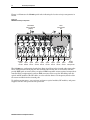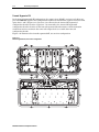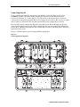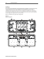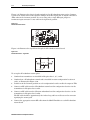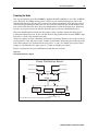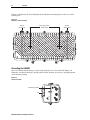
1
Installation and Operation Manual SG4000 1 GHz Modular Optical Node (Revision 3) Caution These servicing instructions are for use by qualified personnel only. To reduce the risk of electrical shock, do not perform any servicing other than that contained in the Installation and Troubleshooting Instructions unless you are qualified to do so. Refer all servicing to qualified service personnel. Special Symbols That Might Appear on the Equipment DANGER INVISIBLE LASER RADIATION WHEN OPEN This is a class I product that contains a class IIIb laser and is intended for operation in a closed environment with fiber attached. Do not look into the optical connector of the transmitter with power applied. Laser output is invisible, and eye damage can result. Do not defeat safety features that prevent looking into the optical connector. PEAK POWER 10 mW CLASS I LASER PRODUCT THIS PRODUCT COMPLIES WITH 21CFR CHAPTER 1 SUBCHAPTER J This product contains a class IIIb laser and is intended for operation in a closed environment with fiber attached. Do not look into the optical connector of the transmitter with power applied. Laser output is invisible, and eye damage can result. Do not defeat safety features that prevent looking into optical connector. This symbol indicates that dangerous voltage levels are present within the equipment. These voltages are not insulated and may be of sufficient strength to cause serious bodily injury when touched. The symbol may also appear on schematics. The exclamation point, within an equilateral triangle, is intended to alert the user to the presence of important installation, servicing, and operating instructions in the documents accompanying the equipment. For continued protection against fire, replace all fuses only with fuses having the same electrical ratings marked at the location of the fuse. FCC Compliance This equipment has been tested and found to comply with the limits for a Class A digital device, pursuant to Part 15 of the FCC Rules. These limits are designed to provide reasonable protection against harmful interference when the equipment is operated in a commercial environment. This equipment generates, uses, and can radiate radio frequency energy and, if not installed and used in accordance with the Installation Manual, may cause harmful interference to radio communications. Operation of this equipment in a residential area is likely to cause harmful interference in which case the user will be required to correct the interference at his/her own expense. CAUTION: Any changes or modifications not expressly approved by Motorola could void the user’s authority to operate this equipment under the rules and regulations of the FCC. Canadian Compliance This Class A digital device complies with Canadian ICES-003. Cet appareil numérique de la classe A est conforme À la norme NMB-003 du Canada. FDA Compliance This product meets the requirements of the Code of Federal Regulations, Title 21, Chapter I, Subchapter J, Sections 1010.2, 1010.3, 1040.10, and 1040.11 CLASS 1 LASER PRODUCT Declaration of Conformity We Motorola, Inc. 101 Tournament Drive Horsham, PA 19044, U.S.A. declare under our sole responsibility that the STARLINE® Model SG4000 to which this declaration relates is in conformity with one or more of the following standards: EMC Standards EN55022 EN55024 EN50083-2 CISPR-22 CISPR-24 EN60825 EN60950 IEC 60950 + A1: 1992 + A2: 1993 + A3: 1995 + A4: 1996 Safety Standards EN60065 following the provisions of the Directive(s) of the Council of the European Union: EMC Directive 89/336/EEC Low Voltage Directive 73/23/EEC WEEE Directive 2002/96/EC Copyright © 2006 by Motorola, Inc. All rights reserved. No part of this publication may be reproduced in any form or by any means or used to make any derivative work (such as translation, transformation or adaptation) without written permission from Motorola, Inc. Motorola reserves the right to revise this publication and to make changes in content from time to time without obligation on the part of Motorola to provide notification of such revision or change. Motorola provides this guide without warranty of any kind, either implied or expressed, including, but not limited to, the implied warranties of merchantability and fitness for a particular purpose. Motorola may make improvements or changes in the product(s) described in this manual at any time. Motorola, the stylized M logo, and STARLINE are registered in the US Patent & Trademark Office. LIFELINE is a trademark of Motorola, Inc. IBM is a registered trademark of International Business Machines Corporation. All other product or service marks are the property of their respective owners. © Motorola, Inc. 2006. Contents Section 1 Introduction Using this Manual ............................................................................................................................................................................ 1-3 Related Documentation................................................................................................................................................................... 1-3 Document Conventions................................................................................................................................................................... 1-4 If You Need Help............................................................................................................................................................................... 1-4 Calling for Repairs ........................................................................................................................................................................... 1-5 Section 2 Overview Housing............................................................................................................................................................................................. 2-2 Mounting Holes ....................................................................................................................................................................... 2-2 Port Locations ......................................................................................................................................................................... 2-3 Gaskets .................................................................................................................................................................................... 2-4 Network Monitoring ......................................................................................................................................................................... 2-5 Options and Accessories................................................................................................................................................................ 2-5 Electronics Package ........................................................................................................................................................................ 2-6 Forward Band .......................................................................................................................................................................... 2-6 Return Band............................................................................................................................................................................. 2-6 Configuration.................................................................................................................................................................................... 2-9 Bandpass Frequency............................................................................................................................................................ 2-10 Station Slope ......................................................................................................................................................................... 2-10 Bandpass Frequency Splits ................................................................................................................................................. 2-11 Forward Path Padding ................................................................................................................................................. 2-11 Level Control ......................................................................................................................................................................... 2-12 Surge Protection and Powering........................................................................................................................................... 2-12 Port Entry ............................................................................................................................................................................... 2-13 SG4000 Installation and Operation Manual ii Contents Section 3 Bench Setup and Operation Forward Path Configuration ............................................................................................................................................................3-3 Forward Split ............................................................................................................................................................................3-5 Forward Redundant Split ........................................................................................................................................................3-8 Forward Segmented 2X.........................................................................................................................................................3-12 Forward Redundant Segmented 2X.....................................................................................................................................3-15 Forward Segmented 4X.........................................................................................................................................................3-19 Return Path Configuration.............................................................................................................................................................3-22 Combined Return...................................................................................................................................................................3-24 Combined Redundant Return...............................................................................................................................................3-27 Split Return.............................................................................................................................................................................3-30 Split Redundant Return.........................................................................................................................................................3-33 Segmented Return.................................................................................................................................................................3-36 Powering the Node .........................................................................................................................................................................3-39 Power Supply Operation .......................................................................................................................................................3-43 Typical Power Supply Configuration...................................................................................................................................3-43 Section 4 Modules SG4000 Optical Modules..................................................................................................................................................................4-1 Installing SG4000 Optical Modules........................................................................................................................................4-1 Removing SG4000 Optical Modules ......................................................................................................................................4-2 Cleaning the Optical Connector .............................................................................................................................................4-2 SG4-R/* Optical Receiver .................................................................................................................................................................4-3 SG4-* Analog Optical Return Path Transmitters ...........................................................................................................................4-7 Nominal Optical Power Test Point Table .......................................................................................................................................4-8 SG4-IFPT Optical Transmitter .........................................................................................................................................................4-8 SG4-EIFPT Optical Transmitter .......................................................................................................................................................4-9 SG4-DFBT Optical Transmitter........................................................................................................................................................4-9 SG4-DFBT3 Optical Transmitter......................................................................................................................................................4-9 SG4-DFBT3-*-CWDM Transmitters .................................................................................................................................................4-9 SG4-DRT-2X Digital Return Transmitter.........................................................................................................................................4-9 SG4000 RF Module .........................................................................................................................................................................4-10 FSB Board ..............................................................................................................................................................................4-12 SG4-PS Power Supply....................................................................................................................................................................4-13 Adding Power Supply Modules ............................................................................................................................................4-14 Embedded Plug-in Module ............................................................................................................................................................4-15 Ingress Control ...............................................................................................................................................................................4-17 Status Monitoring ...........................................................................................................................................................................4-17 SG4000 Installation and Operation Manual Contents iii Section 5 Installation Splicing Fiber ................................................................................................................................................................................... 5-1 Fiber Cables...................................................................................................................................................................................... 5-2 Standard Strand Wire Mounting ..................................................................................................................................................... 5-4 Optional Strand Bracket Mounting................................................................................................................................................. 5-5 Pedestal Mounting ........................................................................................................................................................................... 5-7 Grounding the SG4000 .................................................................................................................................................................... 5-8 Coaxial Cable Installation ............................................................................................................................................................... 5-9 Closing the Housing ...................................................................................................................................................................... 5-10 Appendix A Specifications Appendix B Torque Specifications Abbreviations and Acronyms Figures Figure 1-1 SG4000 – closed ........................................................................................................................................................... 1-1 Figure 1-2 SG4000 – open .............................................................................................................................................................. 1-2 Figure 2-1 SG4000 housing dimensions – front and side view.................................................................................................. 2-2 Figure 2-2 SG4000 mounting holes............................................................................................................................................... 2-2 Figure 2-3 Housing port locations................................................................................................................................................. 2-3 Figure 2-4 Housing gaskets ........................................................................................................................................................... 2-4 Figure 2-5 Signal flow diagram – SG4000 lid ............................................................................................................................... 2-7 Figure 2-6 Signal flow diagram – SG4000 base ........................................................................................................................... 2-8 Figure 2-7 Configuration notation ................................................................................................................................................. 2-9 Figure 2-8 Relative level dB versus 1 GHz slope....................................................................................................................... 2-10 Figure 2-9 Port entry board – seizure mechanism .................................................................................................................... 2-13 Figure 2-10 Port entry board – AC terminal clamp .................................................................................................................... 2-14 Figure 3-1 SG4000 base and major components......................................................................................................................... 3-1 Figure 3-2 SG4000 lid and major components............................................................................................................................. 3-2 Figure 3-3 SG4000 showing major forward-path components................................................................................................... 3-3 Figure 3-4 Forward split, single receiver configuration.............................................................................................................. 3-5 Figure 3-5 Forward split board ...................................................................................................................................................... 3-6 Figure 3-6 Forward split board – signal flow................................................................................................................................ 3-6 SG4000 Installation and Operation Manual iv Contents Figure 3-7 Forward redundant-split, two-receiver configuration................................................................................................3-8 Figure 3-8 Forward redundant-split board....................................................................................................................................3-9 Figure 3-9 Forward redundant-split board – signal flow .............................................................................................................3-9 Figure 3-10 EPIM jumpers.............................................................................................................................................................3-10 Figure 3-11 Forward segmented 2X, two-receiver configuration .............................................................................................3-12 Figure 3-12 Forward segmented 2X board..................................................................................................................................3-13 Figure 3-13 Forward segmented 2X – signal flow ......................................................................................................................3-13 Figure 3-14 Forward redundant segmented 2X configuration ..................................................................................................3-15 Figure 3-15 Forward redundant segmented 2X board ...............................................................................................................3-16 Figure 3-16 Forward redundant segmented 2X – signal flow ...................................................................................................3-16 Figure 3-17 Forward segmented 4X configuration.....................................................................................................................3-19 Figure 3-18 Forward segmented 4X board..................................................................................................................................3-20 Figure 3-19 Forward segmented 4X – signal flow ......................................................................................................................3-20 Figure 3-20 SG4000 major return-path components..................................................................................................................3-22 Figure 3-21 Combined return configuration ...............................................................................................................................3-24 Figure 3-22 Combined return board ............................................................................................................................................3-25 Figure 3-23 Combined return board – signal flow......................................................................................................................3-25 Figure 3-24 Combined redundant return configuration..............................................................................................................3-27 Figure 3-25 Combined redundant return board...........................................................................................................................3-28 Figure 3-26 Combined redundant return – signal flow ..............................................................................................................3-28 Figure 3-27 Split return configuration .........................................................................................................................................3-30 Figure 3-28 2X redundant return configuration board...............................................................................................................3-31 Figure 3-29 2X redundant return – signal flow ...........................................................................................................................3-31 Figure 3-30 Split redundant return configuration ......................................................................................................................3-33 Figure 3-31 2X redundant return board.......................................................................................................................................3-34 Figure 3-32 2X redundant return – signal flow ...........................................................................................................................3-34 Figure 3-33 Segmented return configuration .............................................................................................................................3-36 Figure 3-34 Segmented return board...........................................................................................................................................3-37 Figure 3-35 Segmented return board – signal flow....................................................................................................................3-37 Figure 3-36 Power distribution board – diagram........................................................................................................................3-39 Figure 3-37 Power distribution board..........................................................................................................................................3-40 Figure 3-38 SG4000 – fuse locations...........................................................................................................................................3-41 Figure 3-39 SG4-PS power supply ...............................................................................................................................................3-43 Figure 4-1 SG4-R/* block diagram..................................................................................................................................................4-3 Figure 4-2 SG4-R/* cover on, cover off..........................................................................................................................................4-4 Figure 4-3 Test-point voltage versus optical power ....................................................................................................................4-6 Figure 4-4 SG4-* transmitter block diagram .................................................................................................................................4-7 Figure 4-5 SG4-* transmitter...........................................................................................................................................................4-7 SG4000 Installation and Operation Manual Contents v Figure 4-6 SG4-RF module block diagram ................................................................................................................................. 4-10 Figure 4-7 SG4-RF module........................................................................................................................................................... 4-11 Figure 4-8 FSB board.................................................................................................................................................................... 4-12 Figure 4-9 SG4-PS features.......................................................................................................................................................... 4-13 Figure 4-10 SG4-PS current input and output curves ............................................................................................................... 4-15 Figure 4-11 EPIM board ................................................................................................................................................................ 4-15 Figure 5-1 Service cable connection and compression fitting................................................................................................... 5-1 Figure 5-2 Housing lid and fiber management trays ................................................................................................................... 5-3 Figure 5-3 Fiber management tray ................................................................................................................................................ 5-3 Figure 5-4 Strand mounting clamps – top view ........................................................................................................................... 5-4 Figure 5-5 Strand mounting clamps – front and side view......................................................................................................... 5-5 Figure 5-6 Optional SG2-style mounting bracket – front and side views.................................................................................. 5-6 Figure 5-7 Optional strand bracket – installed............................................................................................................................. 5-7 Figure 5-8 Pedestal or surface mounting ..................................................................................................................................... 5-8 Figure 5-9 Ground connection....................................................................................................................................................... 5-8 Figure 5-10 Center conductor length ............................................................................................................................................. 5-9 Figure 5-11 Housing bolts – torque sequence........................................................................................................................... 5-10 Tables Table 2-1 Options and accessories............................................................................................................................................... 2-5 Table 2-2 SG4000 pad chart-standard gain ................................................................................................................................ 2-12 Table 3-1 SG4000 forward-path configuration options ............................................................................................................... 3-4 Table 3-2 Return-path options ..................................................................................................................................................... 3-23 Table 3-3 SG4 fuses and powering options ............................................................................................................................... 3-42 Table 4-1 SG4-R/* features ............................................................................................................................................................. 4-4 Table 4-2 SG4-R/* minimum output levels.................................................................................................................................... 4-5 Table 4-3 SG4-* transmitter features............................................................................................................................................. 4-8 Table 4-4 SG4-* transmitter models and optical power test point table.................................................................................... 4-8 Table 4-5 SF4-RF module features .............................................................................................................................................. 4-11 Table 4-6 FSB board controls ...................................................................................................................................................... 4-12 Table 4-7 SG4-PS features ........................................................................................................................................................... 4-13 Table 4-8 SG4-PS inputs and outputs......................................................................................................................................... 4-14 Table 4-9 EPIM board user-interface settings............................................................................................................................ 4-16 Table 4-10 SG4000 reporting and control provisions ............................................................................................................... 4-17 Table A-1 SG4000 optical receiver characteristics......................................................................................................................A-1 Table A-2 Station RF characteristics ............................................................................................................................................A-1 Table A-3 SG4000 general characteristics ...................................................................................................................................A-2 Table A-4 AC current requirements ..............................................................................................................................................A-2 Table A-5 DC current requirements ..............................................................................................................................................A-2 SG4000 Installation and Operation Manual vi Contents Table A-6 SG4-PS power requirements........................................................................................................................................ A-3 Table A-7 SG4000 performance, with 77 channels ..................................................................................................................... A-3 Table A-8 SG4-IFPT RF specifications ......................................................................................................................................... A-3 Table A-9 SG4-EIFPT RF specifications....................................................................................................................................... A-4 Table A-10 SG4-DFBT RF specifications...................................................................................................................................... A-4 Table A-11 SG4-DFBT/3 RF specifications .................................................................................................................................. A-4 SG4000 Installation and Operation Manual Section 1 Introduction Motorola’s SG4000 modular optical node is now available with 1 GHz forward actives. Revision 3 of the Installation and Operation Manual includes specific information regarding the 1 GHz models, as well as expanded details on the overall node features and functions. Motorola’s STARLINE® SG4000 modular optical node is the successor to the popular fouroutput SG2440 platform. The optical node performs light wave-to-RF and RF-to-light wave signal conversions in an optical transmission link. The SG4000 enables the system operator to independently and incrementally segment the downstream and upstream sections of the node without discarding the initial platform. This product is designed to support a wide variety of advanced hybrid-fiber/coaxial (HFC) network topologies. The SG4000 node and its associated modules are new designs that build on Motorola’s heritage of performance and reliability. These new modules are not interchangeable with those used in any previous node. Also unique are the mini-auto fuses used to route AC power within the SG4000. The six RF/AC port entry assemblies feature a new 1/16 inch hex-head seizure mechanism to secure the connector. The JXP-B* break-away ergonomic attenuator pads, ingress control switches, and linear mid-stage equalizers used in the SG4000 are common with other Motorola optical nodes. The 1 GHz version contains a new forward receive module, new RF modules, new port entry assemblies, and new forward configuration boards. The SG4-R receiver and SG4-RF modules are denoted by a 1 GHz notation on their respective silk-screened covers. You can identify the new port entry assemblies by a new terminal clamp mechanism that eliminates the use of solder to capture the AC wiring harness. The 1 GHz forward configuration boards also have a shielded cover. More detailed information is provided in subsequent sections of this manual. Figure 1-1 illustrates a closed SG4000 modular optical node. Figure 1-1 SG4000 – closed SG4000 Installation and Operation Manual 1-2 Introduction Figure 1-2 illustrates an open SG4000 telecommunications optical node. Figure 1-2 SG4000 – open Base Lid SG4000 features include: Split, split redundant, segmented 2X, segmented 2X redundant, segmented 4X 870 MHz, and 1 GHz forward passband using up to four optical receivers Combined single, combined redundant, split, split redundant, and segmented return using up to four analog optical transmitters An auxiliary optical module location for future payloads HMS-compatible status monitor transponder location Four independent RF modules located in six RF/AC ports Ingress switching capability through manual or headend control Redundant powering capability without the need for an additional interconnect cable 15 amp power passing User-friendly fiber management 60/90 volt, 50/60 Hz powering Digital return capability Modular plug-in diplex filters and equalizers Custom configuration for unique system requirements SG4000 Installation and Operation Manual Introduction 1-3 Using this Manual The following sections provide information and instructions to install, configure, and operate the SG4000: Section 1 Introduction provides a brief description of the product, identifies the information contained in this manual, and gives the help line telephone number and repair return information. Section 2 Overview provides a list of the options and accessories, housing, and configuration information for the SG4000. Section 3 Bench Setup and Operation provides instructions to complete configuration of the node and set up the options. It describes the bench testing procedures that are recommended before installation. Operational information governing the use of various options and applications required by your system is also presented. Section 4 Modules provides detailed information on the features and use of all modules used in the SG4000. It also provides information regarding their installation, removal, and cleaning of the connectors on optical modules. Section 5 Installation provides instructions for installing the SG4000 in a distribution system. Appendix A Specifications provides technical specifications for the SG4000 node and major options. Appendix B Torque Specifications provides the appropriate torque specifications for the screws, clamps, connectors, and bolts used in the SG4000. Abbreviations and Acronyms The Abbreviations and Acronyms list contains the full spelling of the short forms used in this manual. Related Documentation Although these documents provide information that may be of interest to you, they are not required to install or operate the SG4000. LL-CU HFC MANAGER Control Unit Installation and Operation Manual HFC MANAGER for Windows Site Preparation Guide HFC MANAGER for Windows Software Operations Manual Return Path Level Selection, Setup, and Alignment Procedure Reference Guide SG4-DRT-2X Installation Sheet SG4000 Installation and Operation Manual 1-4 Introduction Document Conventions Before you begin to use the SG4000, familiarize yourself with the stylistic conventions used in this manual: Bold type Indicates text that you must type exactly as it appears or indicates a default value. SMALL CAPS Denotes silk screening on the equipment, typically representing front and rear-panel controls, I/O connections, and indicators (LEDs). * (Asterisk) Indicates that there are several versions of the same model number and the information applies to all models. When the information applies to a specific model, the complete model number is given. Italic type Denotes a displayed variable, a variable that you must type, or is used for emphasis. If You Need Help If you need assistance while working with the SG4000, contact the Motorola Technical Response Center (TRC): Inside the U.S.: 888-944-HELP (1-888-944-4357) Outside the U.S.: 215-323-0044 Motorola Online: http://businessonline.motorola.com The TRC is on call 24 hours a day, 7 days a week. In addition, Motorola Online offers a searchable solutions database, technical documentation, and low-priority issue creation and tracking. Technical Response Center Telephone Menu Options Connected Home Solutions http://businessonline.motorola.com 888-944-HELP / 215-323-0044 Broadcaster, Satellite IRD or Encoder Products PRESS 2 Video Products PRESS 1 PRESS 1 Controllers PRESS 1 Digital PRESS 2 Headend PRESS 3 Set-tops PRESS 1 Commercial IRD PRESS 2 Uplink Encoder PRESS 2 Analog Consumer Products PRESS 4 Data Networks/ Transmission Products PRESS 3 PRESS 1 PRESS 2 PRESS 3 Cable Router Cable Modems Transmission Products VOIP Products Severity Level 1 - Critical Failure 2 - Serious Failure 3 - Lesser Failure 4 - Technical Assistance SG4000 Installation and Operation Manual PRESS 4 Network Management PRESS 5 Multiservice Transport Products (MBT/MWT/MEA) PRESS 1 Consumer Satellite C Band PRESS 2 Broadband Retail Support PRESS 1 PRESS 2 Network Network Licensing Management Products Issued: 04/2005 Introduction 1-5 Calling for Repairs If repair is necessary, call the Motorola Repair Facility at 1-800-227-0450 for a Return for Service Authorization (RSA) number before sending the unit. The RSA number must be prominently displayed on all equipment cartons. The Repair Facility is open from 8:00 AM to 5:00 PM Central Time, Monday through Friday. When calling from outside the United States, use the appropriate international access code and then call 956-541-0600 to contact the Repair Facility. When shipping equipment for repair, follow these steps: 1 Pack the unit securely. 2 Enclose a note describing the exact problem. 3 Enclose a copy of the invoice that verifies the warranty status. 4 Ship the unit PREPAID to the following address: BCS Nogales Repair Center Attn: RSA #_________ 6908 East Century Park Drive Tucson, AZ 85706 US SG4000 Installation and Operation Manual Section 2 Overview This section provides an overview of the multiple receiver and transmitter combinations available to satisfy a variety of architectures. The forward path uses Motorola Proprietary Enhanced Gallium Arsenide (E-GaAs) technology to deliver broadcast video and data over the entire 47 MHz-1 GHz passband. With provisions for up to nine optics modules, the SG4000 scales from its most basic version to full 4x4 capability without any loss of initial investment and with minimal service interruptions. The base SG4000 forward path configuration receives broadcast video and data and splits the content into four RF outputs. As an option, you can add a second receiver to provide module redundancy. The node can be divided in half, with one receiver providing signals to the right half while a second receiver, with unique content, drives the left half. You can add two additional receivers to provide module redundancy for each half. Finally, you can use four receivers in conjunction with dedicated RF modules to provide 4X segmentation. The base SG4000 return path configuration combines all four RF returns using a return combined redundant board and drives a single analog 1310 or 1550 nm transmitter. You can add an additional transmitter to provide return path module redundancy. You can also use a return split redundant board with two transmitters to split the node in half, or you can use four transmitters to add module redundancy to the split return. As a final option, you can use two return segment configuration boards to provide complete return path segmentation. The SG4000 power system uses N+1 redundant power supplies that provide forced load sharing. A single SG4-PS power supply supports the base configuration of four SG4-RF modules, one receiver, one transmitter, embedded plug-in module (EPIM), and a status monitor transponder. You can add a second power supply to provide redundancy for the base configuration. As additional optics modules are added for redundancy or segmentation, a second power supply is required to support the increased payload. You can add a third SG4-PS to provide power supply redundancy in configurations requiring two supplies. The SG4000 power system load sharing design does not support independent AC powering with two sources. To accommodate unique system criteria, the SG4000 is shipped as a configured product. Options available include: Low, standard, and high tilts Band splits S, J, A, K, and E SC/APC or E2000 optical connectors HMS transponder Ingress switches Redundant powering As a platform for Motorola’s high-speed Time Domain Multiplexed (TDM) digital return, the SG4000 effectively combines node segmentation with wavelength aggregation, conserving fiber resources. Digital return transmitters are sold separately. SG4000 Installation and Operation Manual 2-2 Overview Housing The SG4000 optical node is furnished in an aluminum housing that protects the electronics from weather and dissipates internally generated heat. Figure 2-1 illustrates the SG4000 housing and provides its dimensions. Figure 2-1 SG4000 housing dimensions – front and side view 4 16.84 inches 6 5 11.03 inches 23.63 inches 10.59 inches Coaxial cable connections to the housing are made using conventional 5/8 inch × 24 threads per inch stinger-type connectors. For strand mounting, there are two clamps, located 16.84 inches apart, that secure the strand with 5/16 × 20 stainless steel bolts. Mounting Holes Two threaded holes are located on the horizontal center-line on the rear of the housing. These 5/16 × 20 × 3/4 holes are separated by eleven inches center-to-center and can be used for pedestal or surface mounting. Figure 2-2 SG4000 mounting holes 11.00 inches SG4000 Installation and Operation Manual Overview 2-3 Port Locations The six housing ports provide connections for either RF coaxial cables or an external 60 or 90 VAC power supply. The node is shipped with RF modules in the four corner locations, each with an externally accessible –20 dB forward RF test point. Ports 2 and 5 are available for connection to an external power supply. Two ports (one on each end of the housing lid) provide fiber entry. All ports are protected by factory-inserted threaded plugs or plastic cap plugs. Discard these plugs when you install the cable connectors. Figure 2-3 illustrates the housing port locations. Figure 2-3 Housing port locations Test point 3 4 2 Port 3 Lid 5 Port 2 Port 4 Port 5 6 1 Port 1 Test point Port 6 Test point Test point Fiber entry Fiber entry SG4000 Installation and Operation Manual 2-4 Overview Gaskets The housing lid is equipped with an elastomer core, woven-wire RF gasket for EMI shielding and ground continuity. The housing base is equipped with a silicone-rubber gasket to provide an environmental seal between the housing base and lid. Both gaskets must be in place and in good condition to ensure proper operation and protection of the station. The weather gasket should be lightly coated with silicone grease each time the node is opened. Figure 2-4 illustrates the housing gaskets. Figure 2-4 Housing gaskets Weather gasket (silicone rubber) RF gasket (woven wire) SG4000 Installation and Operation Manual Overview 2-5 Network Monitoring The optional LIFELINE Status Monitoring System enables you to monitor the SG4000 from a headend or a remote location. The transponder (LL-SG4) consists of a plug-in module mounted in the lid. The entire LIFELINE system includes: LL-CU control units Connected to the system at the headend and interrogate each SG4000 field transponder with FM outbound and inbound transmissions. A variety of outbound and inbound frequencies can be selected depending on the configuration of the system. The control unit reports this information to the status monitor computer. Status Monitor Computer and Software Includes an IBM®-compatible computer that is connected to the control unit (CU) through an RS-232 link. LIFELINE software enables the operator to view measurements taken by the transponders. LL-SG4-* Field Installed Transponders Installed in individual field components, this unit interfaces with the CU at the headend. It reports parameters, such as forward amplifier DC current draw, AC and DC voltage, management and control of RF ingress switching, and tamper status. Options and Accessories Table 2-1 provides a list of options and accessories for the SG4000. Table 2-1 Options and accessories Model Description Function JXP-B* Fixed attenuator Attenuator pads are used to adjust amplifier levels and are available in 1 dB steps from 1 through 24 dB. The appropriate value must be installed. JXP-ZX 0 dB attenuator This attenuator is used in place of JXP-B* pads when no attenuation is needed. FTEC Crowbar overvoltage protection The FTEC is an electronic crowbar/surge protector. LL-SG4 LIFELINE module This module enables the system operator to monitor the SG4000 from a remote location. See Section 3, “Bench Setup and Operation” for parameters monitored. See the product catalog for additional information. GFAL Test probe This probe is used to evaluate node performance. SG4-EPIM Embedded control module This board controls the ingress switch and receiver A/B redundant switching. SG4-PS Power supply Provides the +24 VDC supply to the station. It has an extended voltage range. SG4SERCAB/* Service cable An 8-fiber service cable that is available with SC/APC connectors. LME-87-* Forward equalizers Used to increase the output tilt of the receiver in an 870 MHz system. They are available in 1 dB increments from 2 dB through 8 dB. SG4000 Installation and Operation Manual 2-6 Overview Model Description Function LME-100-* Forward equalizers Used to increase the output tilt of the receiver in a 1 GHz system. They are available in 1 dB increments from 3 dB through 10 dB. ICS II Ingress switch This switch enables the operator to troubleshoot without shutting down the return path. It requires the use of either the LL-SG4/* or the SG4-EPIM. SG4-R/* Lightwave receiver This receiver converts the received optical signal to broadband RF. SG4-* Analog return transmitters Refer to the list provided in Section 4, “Modules.” SG4-FSB Flatness slope board Provides slope for individual RF modules. Electronics Package Individual RF modules that provide superior port-to-port isolation and improved reliability now replace the traditional one-piece electronics package. Connections to the RF modules are made with double-shielded RG 179 RF cables for the forward and return path signals. The individual RF modules can be driven by multiple combinations of receivers, transmitters, and plug-in configuration boards. Forward Band Forward band configurations use up to four SG4-R receivers in the following combinations: Split Four common RF outputs are served by a single SG4-R/* receiver. Split redundant Four common RF outputs are served by either of two SG4-R/* receivers. Segmented 2X Two SG4-R/* receivers – each drives one pair of RF outputs. Segmented 2X redundant Two pairs of SG4-R/* receivers – each pair drives one pair of RF outputs. Segmented 4X Four SG4-R receivers each drive an individual RF output. Return Band Return band configurations use up to four analog optical transmitters in the following combinations: Combined Single All four RF returns are combined and are input to a single return transmitter. Combined redundant All four RF returns are combined and are input to two return transmitters. Split Two pair of RF returns are combined and each is input to a return transmitter. Split redundant Two pair of RF returns are combined and each is input to two return transmitters. Segmented Each RF return is input to a dedicated return transmitter. SG4000 Installation and Operation Manual Overview 2-7 Figure 2-5 provides a diagram of the signal flow path through the SG4000 lid. Figure 2-5 Signal flow diagram – SG4000 lid Status Monitor (Optional) Optical Input (-3 dBm to +2 dBm) TP (-20 dB) RCVR Slot 1 PAD EQ 0.0 dB -1.0 dB +24.0 dB Optical Input (-3 dBm to +2 dBm) -1.0 dB TP (-20 dB) RCVR Slot 2 PAD EQ 0.0 dB -1.0 dB +24.0 dB -1.0 dB TP (-20 dB) Tx Slot 3 PAD +30.0 dB -0.5 dB 6.0 dB TP (-20 dB) Tx Slot 4 PAD +30.0 dB -0.5 dB 6.0 dB TP (-20 dB) Tx Slot 5 PAD +30.0 dB -0.5 dB 6.0 dB TP (-20 dB) Tx Slot 6 PAD +30.0 dB -0.5 dB 6.0 dB Optical Input (-3 dBm to +2 dBm) RCVR Slot 7 TP (-20 dB) PAD EQ 0.0 dB -1.0 dB +24.0 dB Optical Input (-3 dBm to +2 dBm) RCVR Slot 8 Aux -1.0 dB TP (-20 dB) PAD EQ 0.0 dB -1.0 dB PAD EQ +24.0 dB -1.0 dB SG4000 Installation and Operation Manual 2-8 Overview Figure 2-6 provides a diagram of the signal flow-path through the SG4000 base. Figure 2-6 Signal flow diagram – SG4000 base Port Entry -1.0 dB -0.25 dB RF Module 1 -1.0 dB PAD +23 dB -1.0 dB H RESP LPF ICS PAD -1.5 dB -1.0 dB 0.0 dB L -0.25 dB Port 1 TP (-20 dB) TP -20 Ext. -1.0 dB To Pwr Dist Brd -0.6 dB 20A -0.7 dB Port 2 TP (-20 dB) To Pwr Dist Brd RF Module 3 -1.0 dB PAD +23 dB TP (-20 dB) -1.0 dB H RESP LPF ICS PAD -1.5 dB -1.0 dB 0.0 dB L -0.25 dB 20A TP -20 Ext. -1.0 dB Port 3 -0.6 dB -0.7 dB To Pwr Dist Brd TP (-20 dB) 20A -1.0 dB -0.25 dB RF Module 4 -1.0 dB PAD +23 dB H RESP LPF ICS PAD -1.5 dB -1.0 dB 0.0 dB L -0.25 dB Port 4 TP (-20 dB) -1.0 dB TP -20 Ext. To Pwr Dist Brd -1.0 dB 20A -0.6 dB -0.7 dB Port 5 TP (-20 dB) To Pwr Dist Brd RF Module 6 -1.0 dB PAD +23 dB H RESP LPF ICS PAD -1.5 dB -1.0 dB 0.0 dB L -0.25 dB TP (-20 dB) SG4000 Installation and Operation Manual -0.7 dB 20A TP (-20 dB) -1.0 dB TP -20 Ext. Port 6 -1.0 dB -0.6 dB To Pwr Dist Brd 20A Overview 2-9 Configuration The SG4000 is available in standard configurations. The shipped configuration is noted on the bar code label. Figure 2-7 illustrates the configuration notation. Figure 2-7 Configuration notation Key None X Combined A Combined, redundant B Split C D Split, redundant Segmented Digital return transmitters are purchased separately. Fiber service cable is purchased separately. Standard accessories include FTEC, 20A fuses. Forward Path Key X *The number of power supplies depends on the configuration. Return Path Configuration N A Split, one receiver Split redundant, two receivers Key B Segmented 2X, two receivers N Status Monitor Ready? No, none E Yes, EPIM and Ingress Switches C Segmented 2X redundant, four receivers D Segmented 4X, four receivers E Split, one receiver, two RF outputs F Split, one receiver, three RF outputs Key N S Key L Station Tilt 10 dB Fmin-870 MHz (12 dB Fmin-1 GHz) Key S 12.5 dB Fmin-870 MHz (14.5 dB Fmin-1 GHz) S H 14 dB Fmin-870 MHz (16 dB Fmin-1 GHz) R Ingress switch None Ingress switches Power Supply Standard Redundant* SG4Key 87 Forward Bandwidth Key 870 MHz 100 1 GHz Key Connectorization E E2000 S SC/APC Bandpass Split Analog Return Path Transmitters Key N None A IFPT Isolated FP 0.4 mW (-4 dBm) B C EIFPT Enhanced Isolated FP 1.0 mW (0 dBm) DFBT Distributed Feedback 1.0 mW (0 dBm) S J 5-40 MHz/52-Fmax D DFBT3 Distributed Feedback 2.0 mW (3 dBm) 5-55 MHz/70-Fmax E DFBT3-CWDM-1550nm Distributed Feedback 2.0 mW A 5-65 MHz/85-Fmax K 5-42 MHz/54-Fmax E 5-30 MHz/47-Fmax SG4000 Installation and Operation Manual 2-10 Overview Bandpass Frequency The SG4000 modular optical node is only available in a forward bandpass frequency of 1 GHz. If you are deploying the SG4000 in a system with less than 1 GHz, refer to Figure 2-8 to determine the tilt at the appropriate frequency. For example, the standard node slope of 14.5 dB at 1 GHz equates to 12.5 dB at 870 MHz. Figure 2-8 illustrates the tilt selection chart for 1 GHz bandwidth. Figure 2-8 Relative level dB versus 1 GHz slope Relative level, dB SG4000 1 GHz straight line slope chart 16 15 14 13 12 11 10 9 8 7 6 5 4 3 2 1 0 16.0 dB tilt (H) 14.5 dB tilt (S) 12.0 dB tilt (L) 50 150 250 650 450 550 Frequency, MHz Digital loading is 6 dB below analog levels 350 750 870 1 GHz Station Slope The SG4000 is configured in three standard station slopes, as illustrated in Figure 2-8. The slope is defined as a straight line from Ffwdmin (minimum forward frequency) to 1 GHz. The total station slope is a combination of (1) the receiver output, (2) the forward configuration board, and (3) the SG4-RF module, along with (4) port entry board slope. Modules measured apart from the station may not represent the entire station tilt. Station slopes include: Model Slope (dB)@870 MHz Slope (dB)@1003 MHz L 10 12.0 S 12.5 14.5 H 14 16.0 The SG4-R* receivers use a Linear Midstage Equalizer (LME) to generate slope that is common to all of the SG4-RF modules attached to that particular receiver. The SG4-RF modules contain a Flatness/Slope Board (FSB). SG4000 Installation and Operation Manual Overview 2-11 Bandpass Frequency Splits The SG4000 is configured with sufficient frequency bandsplits to accommodate global requirements. The bandpass split can be determined from the model number, as indicated in the chart below: Model Bandpass Split S 5-40/52 MHz-1 GHz J 5-55/70 MHz-1 GHz A 5-65/85 MHz-1 GHz K 5-42/54 MHz-1 GHz E 5-30/47 MHz-1 GHz The components that determine the bandpass frequency splits include the plug-in diplex filters and the vertical return-path low-pass filters (RPLPF-V-*) located in the SG4-RF modules. The diplex filter provides the node crossover isolation at each port and the return-path low-pass filters suppress any additional forward energy at the input to the return transmitters. Forward Path Padding The pad values presented in Table 2-2 serve as a starting point reference for typical installations. While this chart is prepared specifically for 77-channel loading and standard split configuration, the difference for 110-channel loading is approximately 1 to 2 dB less. If the optical levels are high, or the transmitter’s optical modulation index (OMI) is higher than specified, it may be necessary for you to select a JXP value 1 dB or 2 dB higher for the receiver output pad than is shown in Table 2-2. SG4000 Installation and Operation Manual 2-12 Overview Table 2-2 illustrates the typical padding required for optimum performance with a 79 channel load. Table 2-2 SG4000 pad chart-standard gain Input dBm/mW 40 41 42 43 44 45 46 47 48 49 2.0/1.6 Receiver JXPs RF mod JXPs 10 10 10 9 10 8 10 7 10 6 10 5 10 4 10 3 10 2 10 1 1.5/1.4 Receiver JXPs RF mod JXPs 10 9 10 8 10 7 10 6 10 5 10 4 10 3 10 2 10 1 10 0 1.0/1.3 Receiver JXPs RF mod JXPs 10 8 10 7 10 6 10 5 10 4 10 3 10 2 10 1 10 0 9 0 0.5/1.1 Receiver JXPs RF mod JXPs 10 7 10 6 10 5 10 4 10 3 10 2 10 1 10 0 9 0 8 0 0.0/1.0 Receiver JXPs RF mod JXPs 10 6 10 5 10 4 10 3 10 2 10 1 10 0 9 0 8 0 7 0 –0.5/0.9 Receiver JXPs RF mod JXPs 10 5 10 4 10 3 10 2 10 1 10 0 9 0 8 0 7 0 6 0 –1.0/0.8 Receiver JXPs RF mod JXPs 10 4 10 3 10 2 10 1 10 0 9 0 8 0 7 0 6 0 5 0 –1.5/0.7 Receiver JXPs RF mod JXPs 10 3 10 2 10 1 10 0 9 0 8 0 7 0 6 0 5 0 4 0 –2.0/0.6 Receiver JXPs RF mod JXPs 10 2 10 1 10 0 9 0 8 0 7 0 6 0 5 0 4 0 3 0 –2.5/0.6 Receiver JXPs RF mod JXPs 10 1 10 0 9 0 8 0 7 0 6 0 5 0 4 0 3 0 2 0 –3.0/0.5 Receiver JXPs RF mod JXPs 10 0 9 0 8 0 7 0 6 0 5 0 4 0 3 0 2 0 1 0 For forward segmented 4X padding, see Section 3, “Bench Setup and Operation,” Forward Segmented 4X. Level Control The SG4000 has integrated automatic temperature compensation circuitry. There are no user selectable settings or level set backs required. As the ambient temperature increases or decreases, the node strives to maintain frequency level stability. Surge Protection and Powering The SG4000 is shipped with standard Fast Trigger Electronic Crowbar (FTEC) surge protection. The FTEC triggers at approximately 230 V and presents a short circuit to the line during periods of over voltage. After the AC input voltage returns to normal, the FTEC returns to its open-circuit state. This provides the node with a level of protection against surge currents on the AC line. The same protector is used for all supplies. Powering options include standard and redundant common powering. The SG4000 power supply (SG4-PS) is located in the housing base to optimize heat transfer and to balance the thermal load between the base and the lid. An umbilical cord connects the SG4-PS to the lid router SG4000 Installation and Operation Manual Overview 2-13 board. A flexible power-distribution design enables you to power the node from any of the six RF/AC ports. Using fuses and shunts, you can configure the node to distribute power to the remaining active ports. You can also power the node locally through either end while a second cable-plant power supply loops through the other end of the node. You can power the SG4000 from either 60 VAC or 90 VAC system power supplies. There is no voltage selection jumper to relocate. The 20-ampere fuses, installed at the factory, provide power passing to additional amplifiers. Section 3, “Bench Setup and Operation,” Powering the Node, discusses fusing options that are also diagrammed in Figure 3-36. Figures 3-37 and 3-38 illustrate the location of the fuses. Port Entry The SG4000 housing base features six RF/AC ports that are physically identical. You can power the node from any of these ports and use any port to support an RF module for custom installations. The SG4000 port entry seizure mechanism contains a 1/16-inch hex-head screw that travels within a threaded ferrule to secure the connector. This screw is captive and should not be backed out by using excessive force. Figure 2-9 illustrates a top view of the port entry board and the seizure mechanism. Figure 2-9 Port entry board – seizure mechanism Seizure mechanism SG4000 Installation and Operation Manual 2-14 Overview You can distinguish the SG4000 1 GHz port entry assemblies by the addition of a terminal clamp block on the bottom of the port entry board. The terminal clamp secures the AC wiring that connects each of the port entry assemblies. The 870 MHz port entry assemblies have the AC wiring soldered directly to the board. The terminal clamp design on the 1 GHz model enables field personnel to replace the port entry board if necessary. Figure 2-10 illustrates a bottom view of the port entry board and the AC terminal clamp. Figure 2-10 Port entry board – AC terminal clamp Terminal clamp Ensure that you remove all power to the node before attempting to service the port entry board. SG4000 Installation and Operation Manual Section 3 Bench Setup and Operation Before you install the SG4000, it must be set up to meet the power and configuration requirements for each particular node location. This section presents the set up procedures that are recommended to ensure proper functioning of all components and simplify field installation. This section also provides information concerning the operation of the various options and applications required by your system. Figure 3-1 illustrates the SG4000 optical node indicating the location of major components in the base. Figure 3-1 SG4000 base and major components SG4-RF module SG4-RF module SG4 Status monitor Interconnect Cable (SIC) SG4-PS power supplies SG4 Power Interconnect Cable (PIC) SG4-RF module SG4 power distribution board SG4-RF module SG4000 Installation and Operation Manual 3-2 Bench Setup and Operation Figure 3-2 illustrates the SG4000 optical node indicating the location of major components in the lid. Figure 3-2 SG4000 lid and major components Embedded Plug-In Module (EPIM) Auxilliary Rx optics optics slot #9 slot #8 Rx optics slot #7 Tx optics slot #6 Fiber management tray Tx optics slot #5 Tx optics slot #4 Tx optics slot #3 Rx optics slot #2 Rx optics slot #1 Status monitor transponder The SG4000 uses configuration boards that direct signal flow in the forward and return paths. These configuration boards plug into the main lid router board and are electrically coded to provide HMS path awareness when an optional HMS compatible status monitor transponder is installed. Each configuration board has SMB connectors that accept the RF cabling from the optical and RF modules. The RF cables are color coded to denote each frequency band: red for the return and black for the forward path. To facilitate maintenance, you can insert and remove optical modules, RF modules, and power supplies with the node powered and operational. SG4000 Installation and Operation Manual Bench Setup and Operation 3-3 Forward Path Configuration The following subsections present information to help you configure the forward path of the SG4000. To configure the forward path, you must install configuration-specific boards in forward configuration board locations 1 and/or 4, as illustrated in Figure 3-3. Figure 3-3 illustrates the SG4000 and identifies the location of all major forward-path components. Figure 3-3 SG4000 showing major forward-path components Forward RF -20 dB test point Forward configuration board location #4 Forward JXP attenuator Receiver Forward JXP attenuator Receiver Forward RF -20 dB test point Forward configuration board location #1 SG4000 Installation and Operation Manual 3-4 Bench Setup and Operation You can configure the SG4000 forward path with up to four SG4-R receivers and up to two forward configuration plug-in boards. Each board has a specific function and receiver combination associated with it and is clearly labeled. The forward configuration board, in location 1, services the SG4-R receivers in optics slots 1 and 2, as illustrated in Figure 3-2. The forward configuration board in location 4 services the SG4-R receivers in lid optics slots 7 and 8. For detailed information on the SG4-R receiver, see Section 4, “Modules.” Table 3-1 lists the SG4000 forward-path configuration options. Table 3-1 SG4000 forward-path configuration options Option Forward Path Configuration X Forward split, one receiver A Redundant split, two receivers B Segmented, two receivers C Segmented, redundant, four receivers D Segmented, four receivers SG4000 Installation and Operation Manual Bench Setup and Operation 3-5 The following subsections describe the forward-path configuration options. Forward Split In the standard forward split configuration, a single SG4-R receiver delivers forward broadcast content to a single, forward split configuration board. The forward split board distributes signals to 2, 3, or 4 RF outputs. The single SG4-R must be located in lid optics slot 1. The associated forward split plug-in board is located in lid forward configuration board location 1, as shown in Figure 3-4. Figure 3-4 illustrates the forward split, single receiver configuration. Figure 3-4 Forward split, single receiver configuration SG4000 Installation and Operation Manual 3-6 Bench Setup and Operation Figure 3-5 illustrates the forward split board. Jumpers J6 and J7 are shown in the normal default position that enables signal flow to each output connector. When configuring for three outputs, move J6 to the left position, thereby terminating output connector J5 (Port 2). When configuring for two outputs, move J7 to the upper position, thereby terminating output connector J8 (Port 3). Figure 3-5 Forward split board PORT4 C10 J6 PORT2 C2 R10 R8 C8 J9 R3 C11 R7 C5 T3 T2 C17 C6 R6 R1 C4 C16 R4 R11 J8 C3 T1 C7 R5 C13 R2 C14 J7 C15 J4 Rx C1 C9 R9 RX1 C18 C12 J5 J3 PORT1 PORT3 Figure 3-6 illustrates the signal flow through the forward split board. Loss is measured at 870 MHz. Figure 3-6 Forward split board – signal flow Loss = 8.7 dB PORT4 J6 PORT2 -4.0 dB -4.0 dB Rx1 -0.5 dB -4.0 dB PORT1 J7 PORT3 To set up the forward-split, single-receiver option: 1 Install a single SG4-R receiver in lid optics slot 1, as illustrated in Figure 3-4. 2 Install a forward-split board in the forward configuration board location 1, as illustrated in Figure 3-4. 3 Install an RF cable from the SG4-R receiver to the forward-split board Rx. The RF cable should be approximately five inches long and have black boots on the connector signifying forward path. 4 Connect the appropriate forward RF cables from the SG4-RF modules’ FWD connector (Figure 3-4) to the forward-split board. 5 Repeat Step 4 for any additional active RF modules. 6 Position jumpers J6 and J7 (Figure 3-5) as required for the number of active outputs you are using. SG4000 Installation and Operation Manual Bench Setup and Operation 3-7 7 Ensure that the power interconnect cable (PIC) is properly connected from the lid router board to the center power-distribution board in the node housing base. 8 Route the fiber service cable into the node and fiber tray. 9 Measure the optical input power on the forward pigtail, leaving enough length to connect it to the receiver bulkhead connector. 10 Apply power to the node (See Powering the Node in this section). Allow five to ten seconds for the system self diagnosis to complete. 11 Connect the service cable to the receiver bulkhead connector. 12 Verify that the green LED (ON), located on the top panel of the SG4-R/*, is illuminated to confirm enable status. 13 Using a voltmeter, test the optical input power to the receiver. Figure 4-2 illustrates the optical power test point (FWD T.P.) on the top panel of the SG4-R/* receiver. The scaled voltage at this test point is 1.0 V/mW. 14 Use an RF meter to measure the RF output level at the receiver −20 dB test point. For 0 dBm (1.0 mW) input, the receiver output level is approximately 26 dBmV per channel at 870 MHz. Other output levels are presented in Table 4-2. 15 Select a JXP-* pad from Table 2-2 and insert it into the receiver pad facility. 16 Check all –20 dB test points of the SG4-RF modules connected to the forward split board. The SG4-RF modules are located in the four corners of the node base, as illustrated in Figure 3-1. 17 Determine how much output (excess or shortage) is present at the port with the lowest level and insert the necessary pad into the receiver pad facility. 18 If necessary, adjust level variances between SG4-RF modules by placing a pad at the particular output pad position. SG4000 Installation and Operation Manual 3-8 Bench Setup and Operation Forward Redundant Split In this configuration, the output of two SG4-R receivers deliver forward broadcast content to a single forward redundant-split configuration board. Operation in the redundant mode requires that you install two SG4-R/* receivers: the primary in lid optics slot 1, the secondary in lid optics slot 2. Each SG4-R receives an optical input, but only one receiver has an active RF output based on the Embedded Plug-In Module (EPIM) jumper settings. You must locate the forward redundant-split board in forward configuration board location 1. Figure 3-7 illustrates the forward redundant-split, two-receiver configuration. Figure 3-7 Forward redundant-split, two-receiver configuration SG4000 Installation and Operation Manual Bench Setup and Operation 3-9 Figure 3-8 illustrates the forward redundant-split board. Jumpers J7 and J8 are shown in the normal default position that enables signal flow to each output connector. When configuring for three outputs, move J7 to the left position, thereby terminating output connector J5 (OUT 4). When configuring for two outputs, move J8 to the right position, thereby terminating output connector J6 (OUT 3). Figure 3-8 Forward redundant-split board OUT 1 C16 C2 C14 J6 R9 R5 J10 J8 J5 OUT 4 J7 R7 C5 J4 R3 D2 SEC T1 R1 U1 C10 C20 T2 C18 OUT 2 C3 R2 Q3 C4 R11 C17 C11 R6 R10 R17 C19 C13 C8 R13 Q1 J9 R4 C6 C15 D1 R14 C7 R12 Q2 R15 T3 C12 OUT 3 R8 C9 J3 PRI Figure 3-9 illustrates the signal flow through the forward redundant-split board. Loss is measured at 870 MHz. Figure 3-9 Forward redundant-split board – signal flow Loss = 8.7 dB J7 Out 2 Rx Pri Out 4 -4.0 dB -0.5 dB -4.0 dB Rx Sec -4.0 dB Out 1 Out 3 J8 SG4000 Installation and Operation Manual 3-10 Bench Setup and Operation The EPIM board contains jumpers J4 through J9 (illustrated in Figure 3-10) that determine the primary and secondary receiver. The EPIM then activates receiver one or two based on the jumper position. Refer to Section 4, “Modules,” Embedded Plug-in Module for more information regarding its use. Figure 3-10 illustrates the suitcase jumpers located on the EPIM. Figure 3-10 EPIM jumpers Reset D5 D6 D8 D12 D11 C18 D4 U5 J1 C50 U9 D1 C48 C47 L1 C43 U7 U10 C19 U11 U12 U13 0 U14 J7 SW1 B J6 SW1 A J4 SW1 Auto J5 SW2 Auto J8 SW2 A J9 D3 D7 D9 U17 D10 -40 -6 U4 U28 U8 U1 D2 1 2 3 4 5 6 7 8 S2 U16 U19 U6 U2 C20 U3 S1 U18 U15 SW2 B U29 To set up the forward redundant-split, two-receiver option: 1 Install SG4-R/* receivers in lid optics slots 1 and 2, as illustrated in Figure 3-7. 2 Install a forward redundant-split board in the forward configuration board location 1, as illustrated in Figure 3-7. 3 Connect an RF cable from each SG4-R receiver to the input of the forward redundant-split board. The board has SMB connectors that are labeled primary (PRI) and secondary (SEC). 4 Connect the appropriate forward RF cables from the SG4-RF modules to the forward redundant-split board. 5 Position jumpers J7 and J8 on the forward redundant split board (Figure 3-8) as required for the number of active outputs you are using. 6 Ensure that the PIC cable is properly connected to the lid router board and center power distribution board in the housing base. 7 Ensure that the SIC cable is properly connected to the EPIM and center power distribution board in the housing base, as illustrated in Figure 3-7. 8 Move the jumper on the EPIM board from the SW1 AUTO to the SW1 A position, thereby disabling receiver two. See Section 4, “Modules,” Embedded Plug-in Module for detailed information on the switch and jumper settings. 9 Route the fiber service cable into the node and fiber tray. 10 Measure the optical input power on the primary and secondary forward pigtails, leaving enough length to connect them to the receiver bulkhead connectors. 11 Apply power to the node (see Powering the Node in this section). Allow five to ten seconds for the system self diagnosis to complete. 12 Connect the service cable to the primary and secondary receiver bulkhead connectors. SG4000 Installation and Operation Manual Bench Setup and Operation 3-11 13 Verify that the green LED (ON), located on the top panel of the SG4-R/* in lid optics slot 1, is illuminated to confirm enable status. 14 Using a voltmeter, test the optical input power to the receivers. Figure 4-2 illustrates the optical power test point on the top panel of the SG4-R/* receiver. The scaled voltage at this test point is 1.0 V/mW. 15 Measure the RF output level at the primary receiver –20 dB test point using an RF meter. For 0 dBm (1.0 mW) input, the receiver output level is approximately 26 dBmV per channel at 870 MHz. Other output levels are presented in Table 4-2. 16 Select a JXP-* pad from Table 2-2 and insert it into the receiver pad facility. 17 Check all –20 dB test points of the SG4-RF modules connected to the forward redundant-split board. The SG4-RF modules are located in the four corners of the housing base, as illustrated in Figure 3-7. 18 Determine how much output (excess or shortage) is present at the port with the lowest level and insert the necessary pad into the receiver pad facility. 19 If necessary, adjust level variances between SG4-RF modules by placing a pad at the particular output pad position. 20 Move the jumper on the EPIM board to the SW1 B override position, which turns receiver 1 off. The red fault LED on receiver 1, and the green enable LED on receiver 2, should illuminate. 21 Repeat Steps 15 through 17 and verify that the node output levels are the same as the primary receiver. Adjust the secondary receiver output pad only; do not re-adjust any output padding in the RF modules. 22 Move the jumper on the EPIM board back to the SW1 AUTO position. SG4000 Installation and Operation Manual 3-12 Bench Setup and Operation Forward Segmented 2X In the forward segmented 2X configuration, the output of two SG4-R/* receivers each drive one pair of SG4000 RF outputs. This configuration requires the installation of optical receivers in lid optics slots 1 and 7 (Figure 3-11). Receiver 1 is connected to the forward 2X segmented configuration board in location 1. Receiver 7 is connected to the forward 2X segmented configuration board in location 4. The forward segmented board contains a fixed attenuation circuit that strives to maintain the same node output level as set with other forward configuration boards. Figure 3-11 illustrates the forward segmented 2X, two-receiver configuration. Figure 3-11 Forward segmented 2X, two-receiver configuration SG4000 Installation and Operation Manual Bench Setup and Operation 3-13 Figure 3-12 illustrates the forward segmented 2X board. Jumper J4 is shown in the normal position that enables signal flow to each output connector. When configuring for a single output, move J4 to the lower position, thereby terminating output connector J5 (OUT 1). Figure 3-12 Forward segmented 2X board OUT 2 OUT 1 N O R M T E R M J4 RX Figure 3-13 illustrates the signal flow through the forward segmented 2X board. Loss is measured at 870 MHz. Figure 3-13 Forward segmented 2X – signal flow Out 1 J4 -4.0 dB Rx -4.5 dB Loss = 8.7 dB Out 2 To set up the forward segmented 2X option: 1 Confirm that an SG4-R/* receiver is installed in lid slots 1 and 7. 2 Confirm that two forward segment 2X boards are installed in the forward configuration board locations 1 and 4, as illustrated in Figure 3-11. 3 Install an RF cable from each SG4-R receiver to the respective forward segment 2X board. The RF cable should be approximately five inches long and have black boots on the connector signifying the forward path. 4 Connect the appropriate forward RF cables from the SG4-RF modules to the forward segment 2X board. 5 Position jumper J4 as required for the number of active outputs you are using. In a typical installation, the RF modules in Ports 1 and 3 are connected to the forward segment 2X board in configuration location 1. The RF modules in Ports 4 and 6 are connected to the forward segment 2X board in configuration location 4. 6 Ensure that the PIC cable is properly connected to the lid router board and center power-distribution board in the node base. 7 Route the fiber service cable into the node and fiber tray. SG4000 Installation and Operation Manual 3-14 Bench Setup and Operation 8 Measure the optical input power on the forward pigtails, leaving enough length to connect them to the receiver bulkhead connectors. 9 Apply power to the node (see Powering the Node in this section). Allow five to ten seconds for the system self diagnosis to complete. 10 Connect the service cables to each receiver bulkhead connector. 11 Verify that the green LED (on), located on the top panel of the SG4-R/*, is illuminated to confirm enable status. 12 Using a voltmeter, test the optical input power to the receiver in lid optics slot 1. Figure 4-2 illustrates the optical power test point (FWD T.P.) on the top panel of the SG4-R/* receiver. The scaled voltage at this test point is 1.0 V/mW. 13 Use an RF meter to measure the RF output level at the receiver −20 dB test point. For 0 dBm (1.0 mW) input, the receiver output level is approximately 26 dBmV per channel at 870 MHz. Other output levels are presented in Table 4-2. 14 Select a JXP-* pad from Table 2-2 and insert it into the receiver pad facility. 15 Check all −20 dB test points on the SG4-RF modules on the left side of the node. These modules are connected to the forward segment 2X board in forward configuration location 1. 16 Determine how much output (excess or shortage) is present at the port with the lowest level and insert the necessary pad into the receiver pad facility of receiver 1. 17 If necessary, adjust level variances between output ports by placing a pad at the particular output pad position. 18 Check all −20 dB test points on the SG4-RF modules on the right side of the node. These modules are connected to the forward segment 2X board in configuration location 4. Receiver 7 drives configuration board 4, which is connected to Ports 4 and 6. 19 Determine how much output (excess or shortage) is present at the port with the lowest level and insert the necessary pad into the receiver pad facility of receiver 7. 20 If necessary, adjust level variances between output ports by placing a pad at the particular output pad position. Unbalanced padding can degrade isolation performance. Ensure that equivalent optical power levels are present on each receiver if possible. SG4000 Installation and Operation Manual Bench Setup and Operation 3-15 Forward Redundant Segmented 2X In the forward redundant segmented 2X configuration, the output of two pair of SG4-R/* receivers each drives one pair of SG4000 RF outputs. Operation in this configuration requires the installation of optical receivers in lid optics slots 1, 2, 7, and 8 (Figure 3-14). Receivers in optics slots 1 and 2 are connected to the forward segmented 2X board in configuration location 1. Receivers in optics slots 7 and 8 are connected to the forward segmented 2X board in configuration location 4. Each SG4-R receives an optical input, but only one receiver has an active RF output based on the EPIM jumper settings. Figure 3-14 illustrates the forward redundant segmented 2X configuration. Figure 3-14 Forward redundant segmented 2X configuration SG4000 Installation and Operation Manual 3-16 Bench Setup and Operation Figure 3-15 illustrates the forward redundant segmented 2X board. Jumper J5 is shown in the normal default position that enables signal flow to each output connector. When configuring for a single output, move J5 to the left position, thereby terminating output connector J6 (OUT 2). Figure 3-15 Forward redundant segmented 2X board OUT 1 OUT 2 J5 TERM SEC RX NORM PRI RX Figure 3-16 illustrates the forward redundant segmented 2X signal flow. Loss is measured at 870 MHz. Figure 3-16 Forward redundant segmented 2X – signal flow Out 2 Rx Pri J5 -0.5 dB -4.0 dB -4.5 dB Rx Sec Loss = 8.7 dB Out 1 To set up the forward redundant segmented 2X option: 1 Confirm that SG4-R/* receivers are installed in lid optics slots 1, 2, 7, and 8. 2 Confirm that two forward redundant segmented 2X boards are installed in the forward configuration board locations 1 and 4, as illustrated in Figure 3-14. 3 Install an RF cable from the SG4-R/* in lid optics slot 1 to the primary input of the forward redundant segmented 2X board in configuration location 1. 4 Install an RF cable from the SG4-R/* in lid optics slot 2 to the secondary input of the same configuration board. 5 Install an RF cable from the SG4-R/* in lid optics slot 7 to the primary input of the forward redundant segmented 2X board in configuration location 4. 6 Install an RF cable from the SG4-R/* in lid optics slot 8 to the secondary input of the same configuration board. The RF cables should be approximately five inches long and have black boots on the connector signifying forward path. 7 Connect the appropriate forward RF cables from the RF modules to each forward redundant segmented 2X board. SG4000 Installation and Operation Manual Bench Setup and Operation 8 3-17 Position jumper J5 as required for the number of active outputs you are using. In a typical installation, the RF modules in Ports 1 and 3 are connected to the forward redundant segmented 2X board in configuration location 1. The RF modules in Ports 4 and 6 are connected to the forward redundant segmented 2X board in configuration location 4. 9 Ensure that the PIC cable is properly connected to the lid router board and center power distribution board in the node base. 10 Ensure that the SIC cable is properly connected to the EPIM and center power distribution board in the housing base, as illustrated in Figure 3-14. 11 Move the jumper on the EPIM board from the SW1 auto to the SW1 a position, thereby disabling receiver two. See Section 4, “Modules,” Embedded Plug-in Module for detailed information on the switch and jumper settings. 12 Route the fiber service cable into the node and fiber tray. 13 Measure the optical input power on the primary and secondary forward pigtails leaving enough length to connect them to the receiver bulkhead connectors. 14 Apply power to the node (see Powering the Node in this section). Allow five to ten seconds for the system self-diagnosis to complete. 15 Connect the service cable to the primary and secondary SG4-R/* bulkhead connectors. 16 Verify that the green LED (ON), located on the top panel of the SG4-R/* in lid optics slot 1, is illuminated to confirm enable status. 17 Using a voltmeter, test the optical input power to receiver one. Figure 4-2 illustrates the optical power test point on the top panel of the SG4-R/* receiver. The scaled voltage at this test point is 1.0 V/mW. 18 Measure the RF output level at the primary receiver −20 dB test point using an RF meter. For 0 dBm (1.0 mW) input, the receiver output level is approximately 26 dBmV at 870 MHz. Other output levels are presented in Table 4-2. 19 Select a JXP-* pad from Table 2-2. Insert it into the receiver pad facility. 20 Check all −20 dB test points on SG4-RF modules on the left side of the node. These modules are connected to the forward redundant segment 2X board in forward configuration location 1. 21 Determine how much output (excess or shortage) is present at the port with the lowest level and insert the necessary pad into the receiver pad facility of receiver 1. 22 If necessary, adjust level variances between output ports by placing a pad at the particular output pad position. 23 Move the jumper on the EPIM to the SW1 B override position, which turns receiver 1 off. The red fault LED indicator on receiver 1 and the green enable LED on receiver 2 should illuminate. 24 Repeat Steps 18 through 22 and verify that the node output levels are the same as the primary receiver. Adjust the secondary receiver output pad only; do not re-adjust any output padding in the RF modules. 25 Move the jumper on the EPIM board back to the SW1 AUTO position. SG4000 Installation and Operation Manual 3-18 Bench Setup and Operation 26 Move the jumper on the EPIM board from the SW2 auto to the SW2 A position, thereby disabling receiver 8. See Section 4, “Modules,” Embedded Plug-in Module for detailed information on the switch and jumper settings. 27 Route the fiber service cable into the node and fiber tray. 28 Measure the optical input power on the primary and secondary forward pigtails, leaving enough length to connect them to the receiver bulkhead connectors. 29 Apply power to the node (see Powering the Node in this section). Allow five to ten seconds for the system self diagnostics to complete. 30 Connect the service cable to the primary and secondary receiver bulkhead connectors. 31 Verify that the green LED (ON), located on the top panel of the SG4-R/* in lid optics slot 7, is illuminated to confirm enable status. 32 Using a voltmeter, test the optical input power to the receivers. Figure 4-2 illustrates the optical power test point on the top panel of the SG4-R/* receiver. The scaled voltage at this test point is 1.0 V/mW. 33 Using an RF meter, measure the RF output level at the primary receiver −20 dB test point. For 0 dBm (1.0 mW) input, the receiver output level is approximately a flat 26 dBmV at 870 MHz. Other output levels are presented in Table 4-2. 34 Select a JXP-* pad from Table 2-2 and insert it into the receiver pad facility. 35 Check all −20 dB test points on SG4-RF modules on the right side of the node. These SG4-RF modules are connected to the forward redundant segment 2X board in forward configuration location 4. 36 Determine how much output (excess or shortage) is present at the port with the lowest level and insert the necessary pad into the pad facility of receiver 7 37 If necessary, adjust level variances between output ports by placing a pad at the particular output pad position. 38 Move the jumper on the EPIM board to the SW2 B override position, which turns receiver 7 off. The red fault LED on receiver 7 and the green enable LED on receiver 8 should illuminate. 39 Repeat Steps 33 through 37 and verify that the node output levels are the same as the primary receiver. Adjust the secondary receiver output pad only; do not re-adjust any output padding in the RF modules. 40 Move the jumper on the EPIM board back to the SW2 AUTO position. Unbalanced padding can degrade isolation performance. Ensure that equivalent optical power levels are present on each receiver if possible. SG4000 Installation and Operation Manual Bench Setup and Operation 3-19 Forward Segmented 4X In the forward segmented 4X configuration, four SG4-R/* receivers deliver signals to four SG4000 RF modules. Operation in this configuration requires the installation of optical receivers in lid slots 1, 2, 7, and 8 (Figure 3-17). The receivers in lid optics slots 1 and 2 are connected to the forward segmented 4X board in configuration location 1. The receivers in optics slots 7 and 8 are connected to the forward segment 4X board in configuration location 4. The forward segment configuration board has approximately 6 dB less through-loss than the other forward configuration boards. When configured in the forward segment 4X configuration, place 6 dB of additional attenuation in the forward JXP location of each RF module to maintain equivalent signal levels. Figure 3-17 illustrates the forward segmented 4X configuration. Figure 3-17 Forward segmented 4X configuration SG4000 Installation and Operation Manual 3-20 Bench Setup and Operation Figure 3-18 illustrates the forward segmented 4X board. Figure 3-18 Forward segmented 4X board Figure 3-19 illustrates the signal flow through the forward segmented 4X board. Loss is measured at 870 MHz. Figure 3-19 Forward segmented 4X – signal flow Rx Out Loss = 2.7 dB Rx Out To set up the forward segmented 4X option: 1 Confirm that an SG4-R/* receiver is installed in lid optics slots 1, 2, 7, and 8. 2 Confirm that two forward segment 4X boards are installed in forward configuration board locations 1 and 4, as illustrated in Figure 3-17. 3 Connect an RF cable from each SG4-R/* to the inputs of the forward segmented 4X boards. The RF cable should be approximately five inches long and have black boots on the connector signifying the forward path. 4 Connect the appropriate forward RF cables from the SG4-RF modules to the forward segmented 4X boards. In a typical installation, the RF modules in Ports 1 and 3 are connected to the forward segment 4X board in configuration location 1. The RF modules in Ports 4 and 6 are connected to the forward segment 4X board in configuration location 4. 5 Ensure that the PIC cable is properly connected to the lid router board and center power distribution board in the housing base. 6 Route the fiber service cable into the node and fiber tray. 7 Measure the optical input power on the forward fiber pigtails, leaving enough length to connect them to the receiver bulkhead connectors. 8 Connect the service cable pigtails to the receiver bulkhead connectors. 9 Apply power to the node (see Powering the Node in this section). Allow five to ten seconds for the system self-diagnosis to complete. SG4000 Installation and Operation Manual Bench Setup and Operation 3-21 10 Verify that the green LED (ON), located on the top panel of each SG4-R/*, is illuminated to confirm enable status. 11 Using a voltmeter, test the optical input power to the receivers. Figure 4-2 illustrates the optical power test point on the top panel of the SG4-R/* receiver. The scaled voltage at this test point is 1.0 V/mW. 12 Measure the RF output level at the receiver’s −20 dB RF test point using an RF meter. For 0 dBm (1.0 mW) input, the receiver output level is approximately 26 dBmV at 870 MHz. Other output levels are presented in Table 4-2. 13 Select the appropriate JXP-* pad from Table 2-2. Insert it into each receiver’s pad facility. 14 Check the −20 dB RF test point on the SG4-RF module connected to each receiver. 15 Determine how much output (excess or shortage) is present at each SG4-RF module. If necessary, install the appropriate JXP pad at the output pad location. Unbalanced padding can degrade isolation performance. Ensure that equivalent optical power levels are present on each receiver if possible. SG4000 Installation and Operation Manual 3-22 Bench Setup and Operation Return Path Configuration The following subsections present information to help you configure the SG4000 return path. To configure the return path, you must install configuration-specific boards in return configuration board locations 2 and 3, as illustrated in Figure 3-20. Figure 3-20 illustrates the SG4000 and identifies the location of all major return-path components. Figure 3-20 SG4000 major return-path components Return RF -20 dB test point Port seizure screw Return JXP attenuator Return Transmitter configuration return RF board -20 dB location #3 test point SG4000 Installation and Operation Manual Transmitter return JXP attenuator Return configuration board location #2 Bench Setup and Operation 3-23 You can configure the SG4000 return path using a variety of analog or digital transmitters and up to two configuration plug-in boards in the return configuration board locations. Each board has a specific function and transmitter combination associated with it and is clearly labeled. The return configuration board, in location 2, services the analog transmitters in lid optics slots 3 and 4. The return configuration board in location 3 services the analog transmitters in lid optics slots 5 and 6. For detailed information on the return path transmitters, see Section 4, “Modules.” The SG4000 return path and configuration boards provide the nominal input level to the return path transmitters when 28 dBmV total composite power is present at the node housing ports. Table 3-2 identifies and describes the SG4000 return-path configuration options. Table 3-2 Return-path options SG4000 return-path configuration options include: Option Return Path Configuration N None – no configuration board is provided. However, when the SG4000 is purchased with any other return configuration and none is selected for the transmitter, the appropriate return configuration board is installed. X Combined return – all four RF returns are combined on a single transmitter. A Combined redundant return – all four RF returns are combined on two transmitters. B Split return – two RF returns are combined on one transmitter; the other two RF returns are combined on a second transmitter. C Split redundant return – two RF returns are combined on two transmitters; the other two RF returns are combined on two additional transmitters. D Segmented return – each RF return is directed to an individual transmitter. SG4000 Installation and Operation Manual 3-24 Bench Setup and Operation The following subsections describe the return path configurations. Combined Return In the combined return configuration, two, three, or four RF returns are combined onto a single combined redundant return board located in return configuration board location 2, illustrated in Figure 3-21. This board is also used in the combined redundant return configuration in the next subsection. Figure 3-21 illustrates the combined return configuration. Figure 3-21 Combined return configuration SG4000 Installation and Operation Manual Bench Setup and Operation 3-25 Figure 3-22 illustrates the combined return board required for the combined return configuration. Jumpers J3, J6, and J9 are shown in the normal default position. Jumper J9 enables/disables the signal flow to output connector J10 (TX2). Jumper J9 is shown in the upper position to terminate the output connector path to TX2. The RF output to TX1 is connected to a single return transmitter in lid optics slot 4. Figure 3-22 Combined return board L1 T3 J8 C3 L2 IN1 T2 T1 C15 SM C11 J9 J10 J12 R12 C6 T5 J1 C9 C7 T4 IN3 R15 R21 C10 J11 J2 J5 R14 R13 R10 R9 TX1 C13 J7 TX2 IN2 J6 J3 J4 IN4 Figure 3-23 illustrates the signal flow through the combined return board. Figure 3-23 Combined return board – signal flow Loss = 0.9 dB In1 In2 -3.5 dB Tx2 J3 +11 dB J9 -0.5 dB -3.5 dB Tx1 -3.5 dB +11 dB J6 SM In3 -3.5 dB In4 To set up the combined return option: 1 Confirm that a single transmitter is installed in lid optics slot 4. 2 Confirm that a combined return board is installed in the lid board in return configuration board location 2, as illustrated in Figure 3-21. 3 Position J9 in the upper position to terminate the output to TX2. 4 Connect an RF cable from the combined return board output (TX1) to the transmitter input. The RF cable should be approximately five inches long and have red boots on the connector signifying the return path. 5 Connect the appropriate return RF cables from the SG4-RF modules to the combined return board. 6 Position jumpers J3 and J6 as required by the number of active inputs you are using. SG4000 Installation and Operation Manual 3-26 Bench Setup and Operation Jumper J3 enables/disables IN4 and jumper J6 enables/disables IN2. 7 Ensure that the PIC cable is properly connected to the lid and center power distribution board in the housing base. 8 Route and connect the fiber service cable. 9 Apply power to the node (see Powering the Node in this section). Allow five to ten seconds for the system self-diagnosis to complete. 10 Verify that the green LED (ON), located on the top panel of the transmitter, is illuminated to confirm enable status. Refer to Section 4, “Modules,” for fault LED functions. 11 Measure the RF power at the test point provided on top of the return path transmitter. The −20 dB test point is located after the JXP pad location and indicates the level into the laser. 12 Place the proper JXP pad into the transmitter pad facility to achieve the nominal total power level of −5 dBmV at the test point. 13 Review return-path system levels. The unit is configured to drive the laser to the recommended level (+15 dBmV) when the total combined power at all housing ports is approximately +28 dBmV. 14 Measure the optical power level at the test point provided on the top of the return path transmitter. The scaled voltage at this test point is 1.0 V/mW. SG4000 Installation and Operation Manual Bench Setup and Operation 3-27 Combined Redundant Return In the combined redundant return configuration, two, three, or four RF returns are combined onto a combined redundant return board. The combined redundant return board directs the signals to two return transmitters located in lid optics slots 3 and 4. This board is located in configuration location 2, as shown in Figure 3-24. Figure 3-24 illustrates the combined redundant return configuration. Figure 3-24 Combined redundant return configuration SG4000 Installation and Operation Manual 3-28 Bench Setup and Operation Figure 3-25 illustrates the combined redundant return plug-in board required for combined redundant return configuration. Jumpers J3, J6, and J9 are shown in the normal default position. Jumper J9 enables/disables the signal flow to output connector J10 (TX2). Jumper J9 is shown in the lower position to enable the output connector path to TX2. The RF output to TX1 is connected to a return transmitter in lid optics slot 4. The RF output to TX2 is connected to a return transmitter in lid optics slot 3. Figure 3-25 Combined redundant return board L1 T3 J8 J5 R14 R13 R10 R9 TX1 C3 L2 IN1 T2 T1 C15 SM C11 J9 J10 J12 R12 C6 T5 J1 C9 C7 T4 IN3 R15 R21 J2 C10 J11 C13 J7 TX2 J6 IN2 J3 J4 IN4 Figure 3-26 illustrates the signal flow through the combined redundant return board.: Figure 3-26 Combined redundant return – signal flow Loss = 0.9 dB In1 In2 -3.5 dB Tx2 J3 +11 dB J9 -0.5 dB -3.5 dB Tx1 -3.5 dB +11 dB J6 SM In3 -3.5 dB In4 To set up the combined redundant return option: 1 Confirm that transmitters are installed in lid optics slots 3 and 4. 2 Confirm that a combined redundant return board is installed in the return configuration board location 2, as illustrated in Figure 3-24. 3 Position J9 in the lower position to enable the output to TX2. 4 Connect an RF cable from each of the combined redundant return board outputs to both transmitter inputs. The RF cable should be approximately five inches long and have red boots on the connector signifying the return path. SG4000 Installation and Operation Manual Bench Setup and Operation 5 Connect the appropriate return RF cables from the SG4-RF modules to the combined redundant return board. 6 Position jumpers J3 and J6 as required by the number of active inputs you are using. 3-29 Jumper J3 enables/disables IN4 and jumper J6 enables/disables IN2. 7 Ensure that the PIC cable is properly connected to the lid router board and center power distribution board in the housing base. 8 Route and connect the fiber service cables. 9 Apply power to the node (see Powering the Node in this section). Allow five to ten seconds for the system self-diagnosis to complete. 10 Verify that the green LED (ON), located on the top panel of each transmitter, is illuminated to confirm enable status. Refer to Section 4, “Modules,” for fault LED functions. 11 Measure the RF power at the test point on the top of each return path transmitter. The −20 dB test points are located after the JXP pad location and indicate the level into the transmitter. 12 Place the proper JXP pads into the transmitter pad facilities to achieve the nominal total power level of −5 dBmV at the test point. 13 Review return-path system levels. The unit is configured to drive the laser to the recommended level (+15 dBmV) when the total combined power at all housing ports is approximately +28 dBmV. 14 Measure the optical power level at the test point on the top of each return path transmitter. The scaled voltage at this test point is 1.0 V/mW. SG4000 Installation and Operation Manual 3-30 Bench Setup and Operation Split Return In the split return configuration, each pair of RF returns is applied to a separate 2X redundant return configuration board. The 2X redundant return configuration board, in return configuration board location 2, directs RF to the transmitter in lid optics slot 3. The 2X redundant return configuration board, in return configuration board location 3, directs RF to the transmitter in lid optics slot 6. The same configuration board is used in the 2X redundant return configuration explained in the next subsection. Figure 3-27 illustrates the split return configuration. Figure 3-27 Split return configuration SG4000 Installation and Operation Manual Bench Setup and Operation 3-31 Figure 3-28 illustrates the 2X redundant return configuration board. Jumpers J5 and J6 are shown in the normal default position. Jumper J6 enables/disables signal flow to output connector J8 (TX2). Jumper J5 terminates input connector J3 (IN2) when only a single RF input is used. Figure 3-28 2X redundant return configuration board IN2 C9 IN1 C3 R4 C2 C18 L1 R2 C12 T2 SM R11 J9 T3 TX1 R16 C19 R12 R13 C4 R15 Q1 C11 R7 J7 C1 R10 C17 C14 R14 R5 C15 J6 TERM C10 J1 J4 R1 C16 J8 C13 R8 TX2 J5 R6 R3 C6 TERM J2 C5 J3 C7 C8 T1 Figure 3-29 illustrates the signal flow through the 2X redundant return board. Figure 3-29 2X redundant return – signal flow TX2 IN2 J6 -0.5 dB J5 -3.5 dB -3.5 dB +7.5 dB TX1 SM IN1 Loss = 0.9 dB To set up the return 2X redundant option: 1 Confirm that return transmitters are installed in lid optics slots 3 and 6. 2 Confirm that a 2X redundant return board is installed in lid return configuration board locations 2 and 3, as illustrated in Figure 3-27. 3 Position J6 in the right-most position to terminate the output to TX2. 4 Connect an RF cable from the 2X redundant return board, in lid return configuration board location 2, to the transmitter in lid optics slot 3. 5 Connect an RF cable from the 2X redundant return board, in lid return configuration board location 3, to the transmitter in lid optics slot 6. The RF cable should be approximately five inches long and have red boots on the connector signifying the return path. 6 Connect the appropriate return RF cables from the SG4-RF modules to each 2X redundant board. SG4000 Installation and Operation Manual 3-32 Bench Setup and Operation In a typical installation, the RF modules in Ports 1 and 3 are connected to the 2X redundant return board in return configuration location 3. The RF modules in Ports 4 and 6 are connected to the 2X redundant return configuration board in configuration location 2. 7 Ensure that the PIC cable is properly connected to the lid and center power distribution board in the housing base. 8 Route and connect the fiber service cable. 9 Apply power to the node (see Powering the Node in this section). Allow five to ten seconds for the system self-diagnosis to complete. 10 Verify that the green LED (ON), located on the top panel of each transmitter, is illuminated to confirm enable status. Refer to Section 4, “Modules” for fault LED functions. 11 Measure the RF power at the test point on the top of each return path transmitter. The −20 dB test point is located after the JXP pad location and indicates the level into the transmitter. 12 Place the proper JXP pad into each transmitter pad facility to achieve the nominal total power level of −5 dBmV at the test point. 13 Review return path system levels. The transmitter is configured to drive the laser to the recommended level (+15 dBmV) when the total combined power at the housing ports connected to the split return board is approximately (+28 dBmV). 14 Measure the optical power level at the DC test point using a multimeter. The scaled voltage at this test point is 1.0 V/mW. SG4000 Installation and Operation Manual Bench Setup and Operation 3-33 Split Redundant Return In the split redundant return configuration, each pair of RF returns is applied to a separate 2X redundant return configuration board. The 2X redundant return board, in return configuration location 2 (Figure 3-30), directs RF to two transmitters in lid optics slots 3 and 4. The 2X redundant return board, in return configuration location 3, directs RF to two transmitters located in lid optics slots 5 and 6. Figure 3-30 illustrates the split redundant return configuration. Figure 3-30 Split redundant return configuration SG4000 Installation and Operation Manual 3-34 Bench Setup and Operation Figure 3-31 illustrates the plug-in board required for the 2X redundant return option. Jumpers J5 and J6 are shown in the correct position. Jumper J6 enables signal flow to output connector J8 (TX2) when in the left-most position. If you are using only a single RF input, jumper J5 terminates input connector J3 (IN2) when in the right-most position. Figure 3-31 2X redundant return board IN2 C9 IN1 C3 R4 C2 C18 L1 R2 C12 T2 SM R11 J9 T3 TX1 R16 C19 R12 R13 C4 R15 Q1 C11 R7 J7 C1 R10 C17 C14 R14 R5 C15 J6 TERM C10 J1 J4 R1 C16 J8 C13 R8 TX2 J5 R6 R3 C6 TERM J2 C5 J3 C7 C8 T1 Figure 3-32 illustrates the signal flow through the 2X redundant return board. Figure 3-32 2X redundant return – signal flow TX2 IN2 J6 -0.5 dB J5 -3.5 dB -3.5 dB +7.5 dB TX1 SM IN1 Loss = 0.9 dB To set up the 2X redundant return option: 1 Confirm that transmitters are installed in lid optics slots 3, 4, 5, and 6. 2 Confirm that a 2X redundant return board is installed in return configuration locations 2 and 3, as illustrated in Figure 3-30. 3 Position J6 in the left-most position on each configuration board to enable the output to TX2. 4 Connect an RF cable from the 2X redundant return board in configuration location 2 to the transmitters in lid optics slots 3 and 4. 5 Connect an RF cable from the 2X return redundant board in configuration location 3 to the transmitters in lid optics slots 5 and 6. The RF cable should be approximately five inches long and have red boots on the connector signifying the return path. 6 Connect the appropriate return RF cables from the SG4-RF modules to each 2X redundant return board. SG4000 Installation and Operation Manual Bench Setup and Operation 3-35 In a typical installation, the RF module in Ports 1 and 3 are connected at the 2X redundant return board in configuration location 3. The RF modules in Ports 4 and 6 are connected to the 2X redundant return board in configuration location 2. 7 Ensure that the PIC cable is properly connected to the lid and center power distribution board in the housing base. 8 Route and connect the fiber service cable. 9 Apply power to the node (see Powering the Node in this section). Allow five to ten seconds for the system self-diagnosis to complete. 10 Verify that the green LED (ON), located on the top panel of each transmitter, is illuminated to confirm enable status. Refer to Section 4, “Modules,” for fault LED functions. 11 Measure the RF power at the test point on the top of each return path transmitter. The −20 dB test point is located after the JXP pad location and indicates the level into the transmitter. 12 Place the proper JXP pad into each transmitter pad facility to achieve the nominal total power level of −5 dBmV at the test point. 13 Review return path system levels. The transmitter is configured to drive the laser to the recommended level (+15 dBmV) when the total combined power at the housing ports connected to the split redundant return board is approximately +28 dBmV. 14 Measure the optical power level at the DC test point using a multimeter. The scaled voltage at this test point is 1.0 V/mW. SG4000 Installation and Operation Manual 3-36 Bench Setup and Operation Segmented Return In the segmented return configuration, each RF return is applied to an individual transmitter. Two segmented return boards are required. The segmented return boards contain two independent RF paths. The segmented return board installed in return configuration location 2 directs RF to the transmitters located in lid optics slots 3 and 4. The segmented return board in return configuration location 3 directs RF to the transmitters located in lid optics slots 5 and 6. Figure 3-33 illustrates the segmented return configuration. Figure 3-33 Segmented return configuration SG4000 Installation and Operation Manual Bench Setup and Operation 3-37 Figure 3-34 illustrates the segmented return plug-in board. Figure 3-34 Segmented return board IN2 IN1 C4 C7 C1 C9 C12 R2 R9 R3 C2 T1 R10 C8 C3 R11 R4 J5 J6 SM C6 C10 R7 R5 R6 R8 J4 C12 C11 J7 R1 J3 TX2 TX1 Figure 3-35 illustrates the signal flow through the segmented return board. Figure 3-35 Segmented return board – signal flow TX2 Pad IN2 -0.5dB TX1 IN1 Pad Loss = 0.9 dB SM To set up the segmented return option: 1 Confirm that return transmitters are installed in lid optics slots 3, 4, 5, and 6. 2 Confirm that a segmented return board is installed in the return configuration locations 2 and 3, as illustrated in Figure 3-33. 3 Connect an RF cable from the segmented return board in configuration location 2 to the transmitters in lid optics slots 3 and 4. 4 Connect an RF cable from the segmented return board in configuration location 3 to the transmitters is lid optics slots 5 and 6. The RF cable should be approximately five inches long and have red boots on the connector signifying the return path. 5 Connect the appropriate return RF cables from the SG4-RF modules to each segmented return board. In a typical installation, the RF modules in Ports 1 and 3 are connected to the segmented return board in return configuration location 3. The RF modules in Ports 4 and 6 are connected to the segmented return board in return configuration location 2. 6 Ensure that the PIC cable is properly connected to the lid and power distribution board in the housing base. 7 Route and connect the fiber service cable. SG4000 Installation and Operation Manual 3-38 Bench Setup and Operation 8 Apply power to the node (see Powering the Node in this section). Allow five to ten seconds for the system self-diagnosis to complete. 9 Verify that the green LED (ON), located on the top panel of each transmitter, is illuminated to confirm enable status. Refer to Section 4, “Modules,” for fault LED functions. 10 Measure the RF power at the test point on the top of each return path transmitter. The −20 dB test point is located after the JXP pad location and indicates the level into the transmitter. 11 Place the proper JXP pad into each transmitter pad facility to achieve the nominal total power level of −5 dBmV at the test point. 12 Review return path system levels. The transmitter is configured to drive the laser to the recommended level (+15 dBmV) when the total combined power at the housing ports connected to each leg of the segmented return board is approximately +28 dBmV. 13 Measure the optical power level at the DC test point using a multimeter. The scaled voltage at this test point is 1.0 V/mW. For more specific information regarding return path setup procedures, refer to the supplemental document Return Path Level Selection, Setup, and Alignment Procedure. SG4000 Installation and Operation Manual Bench Setup and Operation 3-39 Powering the Node You can conveniently power the SG4000 by applying 60 VAC or 90 VAC to any of the six RF/AC ports. Typically, the middle housing ports, 2 and 5, are not used for RF purposes and are the default powering ports. All six ports are rated at 15 amperes maximum, and each port is fused with a blade-type 20-ampere mini-auto fuse. AC is never transferred onto the RF modules; the port entry boards direct the AC to the power distribution board in the housing base. Removing the fuse at any port removes the AC path from that port to the power distribution board. The power distribution board contains the jumper, shunt, and fuses required to direct power passing throughout the node. It also contains the Fast Trigger Electronic Crowbar (FTEC) surge protection, as well as DC and AC test points. All power supplies use N+1 redundancy and forced load sharing. Therefore, the node can only be powered from a single AC power source. Jumper J8 determines which side physically powers the node. When jumper J8 is positioned to the left, ports 1, 2, and 3 are eligible power ports. When jumper J8 is positioned to the right, ports 4, 5, and 6 are eligible power ports. Figure 3-36 diagrams the power distribution board and fuse locations. Figure 3-36 Power distribution board – diagram Power Distribution Board From Port 1 From Port 4 From Port 3 From Port 6 From Port 2 20 Amp Shunt 20 Amp F3 F1 F2 From Port 5 JUMPER - J8 SIC AC test point - J20 Power Supply #1 +24V Power Supply #2 +24V Power Supply #3 +24V FTEC PIC DC test point - J21 Fuses and/or shunts used as required by application SG4000 Installation and Operation Manual 3-40 Bench Setup and Operation Figure 3-37 illustrates the power distribution board and fuse locations. Figure 3-37 Power distribution board PS1 E4 +24V AC DC test point AC test point SG4000 Installation and Operation Manual J8 PS2 PS3 E2 E3 E1 F3 F1 F2 FTEC Bench Setup and Operation 3-41 Figure 3-38 illustrates the fuse locations in the SG4000 node. Figure 3-38 SG4000 – fuse locations Port 1 Port 2 Port 3 fuse fuse fuse F3 F1 Port 6 Port 5 Port 4 fuse fuse fuse F2 5 Vdc fuse SG4000 Installation and Operation Manual 3-42 Bench Setup and Operation CAUTION! Voltages up to 90 VAC are accessible. To avoid shock hazard, confirm that no power is applied to the node before removing cover or replacing fuses. Table 3-3 identifies and describes the SG4 fuses and powering options. Table 3-3 SG4 fuses and powering options Fuse Location Function Rating Type Port 1 Passes AC to/from Port 1 of the housing base. 20 A, 32 VDC Plug-in, fast blow, mini-auto Port 2 Passes AC to/from Port 2 of the housing base. 20 A, 32 VDC Plug-in, fast blow, mini-auto Port 3 Passes AC to/from Port 3 of the housing base. 20 A, 32 VDC Plug-in, fast blow, mini-auto Port 4 Passes AC to/from Port 4 of the housing base. 20 A, 32 VDC Plug-in, fast blow, mini-auto Port 5 Passes AC to/from Port 5 of the housing base. 20 A, 32 VDC Plug-in, fast blow, mini-auto Port 6 Passes AC to/from Port 6 of the housing base. 20 A, 32 VDC Plug-in, fast blow, mini-auto Shunt F1 Installed — passes AC power from the left to the right side of the node. Removed — isolates the right and left halves so you can loop a different AC source through the side of the node that is not powered. 30 A, 32 VDC Plug-in, fast blow, mini-auto F2 Passes AC power from Port 5 to the rest of the node and must be in place to power the node from the right side. 20 A, 32 VDC Plug-in, fast blow, mini-auto F3 Passes AC power from Port 2 to the rest of the node and must be in place to power the node from the left side. 20 A, 32 VDC Plug-in, fast blow, mini-auto FTEC Provides an over voltage clamp to ground. 230 V FTEC Jumper J8 Determines whether AC power is supplied from the left or right side of the node. N/A Jumper Lid router board Protects the +5 V supply. 1 A, 32 VDC Plug-in, fast blow, mini-auto SG4000 Installation and Operation Manual Bench Setup and Operation 3-43 Power Supply Operation You can power the SG4000 from 60 VAC or 90 VAC system supplies. The SG4000 power supply module is auto-ranging and requires no start-up voltage jumper selection. The power supplies begin to operate when the proper input voltage level of 44 VAC rms is reached; they continue to operate until the input voltage drops below 39 VAC. The line frequency must be 50 Hz or 60 Hz, and the input voltage waveshape must be quasi-squarewave. CAUTION! Damage to the power supply may result from the use of sine wave input power. There are no user-serviceable parts within the SG4-PS power supply. The power supply features a self-protection attribute that shuts it down for instantaneous line voltages higher than 176 VAC. A precision output regulator protects against overcurrent and short circuits, thus providing a precise output voltage. Figure 3-39 SG4-PS power supply ASSEMBLED IN MEXICO CAUTION AC TEST POINT SG4-PS ADJ 24.3V 24V adjust TEST POINT V OLTAGE S IN E XCE SS OF 150 VO LTS ARE P RE SE NT UNDE R COVE R AND M AY BE P RESENT AFTER P OWE R IS RE MO VE D Embedded signal cable NO US ER SERVICABLE PA RTS INSID E SEE INSTAL LATIO N M AN UAL FO R SE RVICE AC/DC cable DC test point AC test point Status LED A single SG4-PS power supply provides 2.9 A at +24 VDC. You can use the test point on the top panel to verify the output. A green LED on the top panel indicates that the power supply is functioning properly. The power supply is factory calibrated for 24 VDC, and no output voltage adjustment is required. If the green LED is not illuminated, the power supply is not producing a 24VDC output. You can use the AC test point on the top panel to determine if the unit is receiving an AC input. If no AC is present, use the AC test point located on the power distribution board to verify that AC is reaching the power supply. Typical Power Supply Configuration In a typical configuration, the SG4 is powered from housing Port 2 and may contain one or two SG4-PS power supplies. To power the node from Port 2: 1 Install a 20 A fuse in housing port 2. 2 Move jumper J8 to the left position. 3 Ensure fuse F3 (20 A): is in place to direct AC to the other ports of the node. is removed to disable AC from the rest of the node. SG4000 Installation and Operation Manual 3-44 4 Bench Setup and Operation Ensure shunt F1 (30 A): is in place to direct AC to the right side of the node. is removed to disable AC from passing to the right side of the node. If powering the node from Port 2 and you remove F3, F1 can still direct AC from Ports 1 and 3 to the rest of the node. SG4000 Installation and Operation Manual Section 4 Modules This section identifies and provides detailed information on all modules that you can use with the SG4000. It also discusses their installation, removal, and cleaning of the optical connectors where appropriate. All of the SG4000 optical modules are equipped with SC/APC connectors but may be ordered with SC to E2000 adaptors. SG4000 Optical Modules The forward path optical modules include: SG4-R forward path optical receiver The return path optical transmitter modules include: SG4-IFPT — isolated Fabry-Perot, 0.4 mW, 1310 nm SG4-EIFPT — enhanced, isolated Fabry-Perot, 1.0 mW, 1310 nm SG4-DFBT and SG4-DFBT3 — isolated Distributed Feedback, 1.0 and 2.0 mW respectively, 1310 nm SG4-DFBT3-*-CWDM — isolated Distributed Feedback, 2.0 mW, eight 1550 nm wavelengths SG4-DRT-2X — 6.3 mW, DWDM ITU channel, 2X TDM digital return Installing SG4000 Optical Modules The SG4000 optical modules design enables you to install them while the node is in service. The module’s flat bottom provides an excellent thermal transfer surface and has locating holes that align with guide pins in the lid of the node. To install an optical module: 1 Determine the proper slot for the module by referring to Section 3, “Bench Setup and Operation,” and Figure 3-2. 2 Position the module in the appropriate slot and press gently on the casting until it is fully seated. 3 Tighten the three 1/4 inch mounting bolts to 8–12 in-lbs to secure the module in the SG4000 lid. 4 Remove the dust covers from the service cable connector and the module’s optical connector. 5 Carefully clean the optical connector using a suitable optical cleaning kit. 6 If necessary, check the optical power levels. 7 Connect the service cable to the module’s optical connector. 8 Attach the appropriate RF cabling to the optics module. 9 Check and align the RF levels in accordance with system requirements and procedures. SG4000 Installation and Operation Manual 4-2 Modules Removing SG4000 Optical Modules The SG4000 optical modules design enables you to remove them while the node is in service. CAUTION! The module surfaces may be hot. Allow sufficient time for the module to cool before handling. To remove an optical module: 1 Disconnect the service cable from the optical connector assembly on the module. 2 Place dust covers on the service cable connector and on the modules’ optical connector assembly. 3 Loosen the three mounting bolts that secure the optical module in the SG4000 lid. 4 Remove the appropriate RF cabling from the module. 5 Pull the module from the SG4000 lid. Cleaning the Optical Connector You can clean the SG4000 optical module connectors easily, without removing the module from the node. To clean the connector: 1 If necessary, disconnect the service cable from the modules’ optical connector assembly. 2 Place a dust cover on the service cable connector. 3 Compress the metal tab to release the optical connector assembly from the module bracket and pull it out of the bracket. CAUTION! Do not pull the optical connector out more than two inches from the casting wall. If you pull the connector out too far, you must disassemble the module and respool the fiber. 4 Carefully clean the optical connector and bulkhead adapter using a suitable optical connector cleaning kit. If an optical connector cleaning kit is not available, clean the connector using pure isopropyl alcohol (99%) and a lint-free wipe. Dry it with filtered compressed air. You can also clean the bulkhead adapter using filtered compressed air. 5 Snap the optical connector assembly back into the module bracket. 6 If necessary, clean and reconnect the service cable. SG4000 Installation and Operation Manual Modules 4-3 SG4-R/* Optical Receiver The SG4-R/* is a line of forward-path optical receivers used in the SG4000 node platform. It is designed for use with a Motorola Omnistar GX2® or similar optical transmitter. The SG4-R/* line delivers the high output levels required in the SG4000. The two-stage receiver uses an integrated optical-hybrid photodetector and a push-pull amplifier for improved RF performance over the entire 40 MHz through 1 GHz passband. It is enabled and disabled in response to a signal from the embedded plug-in module (EPIM). This provides excellent isolation, improved reliability, and reduced power consumption when the receiver is used in redundant applications. The SG4-R/* is equipped with special drive circuitry that provides thermal compensation, thus eliminating the need to make any set-up adjustments or gain set-backs. The wavelength selection jumper is factory-set and provides optimum calibration in a 1310 nm system but is scaled accordingly for 1550 nm. If you need to reset the jumper, move it to the preferred position as illustrated in Figure 4-2. Figure 4-1 illustrates a functional block diagram of the SG4-R/* receiver. Figure 4-1 SG4-R/* block diagram Module enabled +5V SPI interface Microprocessor Module fault +24V Module enable Module enable logic Hybrid current monitor TP -20 dB JXP Optical input -3 to +2 dBm Optical receiver hybrid Optical power monitor Matching network Slope RFTemp Comp Hybrid RF output Optical power test point (1 V/mW) SG4000 Installation and Operation Manual 4-4 Modules Figure 4-2 illustrates the SG4-R/* receiver with the cover installed (left) and the cover removed (right). Figure 4-2 SG4-R/* cover on, cover off RF TP ENABLE LEDs RF test point ON FAULT FAULT LME Wavelength selection jumper SLOPE 1550 1310 Optical power test point 1V/mW OPTICAL INPUT JXP attenuator 1 GHz OPTICAL RECEIVER Table 4-1 provides additional information on the user-related features of the SG4-R/*. Table 4-1 SG4-R/* features Feature Description Wavelength selection jumper Used with 1310 nm or 1550 nm transmitters, the wavelength selection jumper on top of the SG4-R/* optimizes the optical power test point and optical power status indicator calibration for the system wavelength. Note that the jumper has no effect on the optical-to-RF performance (gain, flatness, and slope) of the module. Optical power test point Enables monitoring of the optical power level at the input to the module. The nominal scale factor is 1.0 V/mW. Receiver JXP attenuator JXP style interstage pad that enables you to make forward path gain adjustments. RF output test point -20 dB test point that enables you to measure carriers throughout the forward band. Receiver enable A green LED (ON) that provides visual indication of the receiver’s enable status. Fault indicator A red LED that illuminates when the module is disabled. Linear Mid-stage Equalizer Passive plug-in board that helps develop the overall station slope and affects all of the RF modules attached to the receiver. You can access the LME by removing the receiver chassis cover. SG4000 Installation and Operation Manual Modules 4-5 Table 4-2 provides SG4-R* minimum output levels; levels at the receiver test point are -20 dB. Table 4-2 SG4-R/* minimum output levels Optical input level (dBm/mW) TP Volts (1 mW=1 V) Output (dBmV) @ 547.25 MHz 77 channels Comments 3.0/2.0 2.0 52 High level alarm 2.0/1.58 1.58 50 Normal 1.5/1.4 1.4 49 Normal 1.0/1.26 1.26 48 Normal 0.5/1.1 1.1 47 Normal 0.0/1.00 1.00 46 Optimum –0.5/0.9 0.9 45 Normal –1.0/0.8 0.8 44 Normal –1.5/0.71 0.71 43 Normal –2.0/0.6 0.6 42 Normal –2.5/0.56 0.56 41 Normal –3.0/0.5 0.5 40 Normal –3.5/0.44 0.44 39 Normal –4.0/0.4 0.4 38 Normal –5.0/0.3 0.3 36 Low level alarm Optical modulation index (OMI) for 77 channels (per channel): 0.0403. For 1550 nm operation, the RF levels out of the transmitter will be 0.42 dB higher at any given optical input. OMI for 110 channels (per channel): 0.0337. Optical transmitter wavelength is 1310 nm. The plug-in Linear Mid-Stage Equalizer (LME) circuitry within the SG4-R receiver develops a portion of the overall node output slope and is factory selected depending on the station slope requirements. For a standard slope of 12.5 dB at 870 MHz (14.5 dB at 1003 MHz), the receiver output typically exhibits 8 dB output slope at 870 MHz. The balance of the station slope is generated by the Flatness Slope Board (FSB) in the RF modules. SG4000 Installation and Operation Manual 4-6 Modules Figure 4-3 illustrates the relationship between test-point voltage (Vdc) and optical power (dBm). Figure 4-3 Test-point voltage versus optical power 5 4 Optical power (dBm) 3 2 1 0 -1 -2 -3 -4 -5 -6 0.25 0.50 0.75 1.00 1.25 1.50 1.75 2.00 2.25 Test point DC Voltage (Vdc) 1 Volt = 1 mW optical power 10 Log10 x Voltage (DC) = optical power (dBm) SG4000 Installation and Operation Manual 2.50 2.75 3.00 Modules 4-7 SG4-* Analog Optical Return Path Transmitters The analog SG4000 analog optical return transmitters are single wide modules that feature either Fabry-Perot or Distributed Feedback lasers, depending on the level of performance required. The physical form factor of each transmitter is identical and shown in Figure 4-4. These transmitters have an integrated RF amplifier and all the active circuitry required to provide RF drive to the laser, enabling optimized performance while minimizing set-up time. All transmitters incorporate a microprocessor-controlled circuit to minimize any variation in the optical modulation index (OMI) as the laser slope efficiency changes due to ambient temperature variations. An optical output power DC voltage test point and RF input test point are accessible through the top panel of the transmitter. RF drive level adjustments are accomplished with a JXP style attenuator pad. Figure 4-4 illustrates a functional block diagram of a typical SG4-* transmitter. Figure 4-4 SG4-* transmitter block diagram Optical power sense signal (1.0 V/mW) Test Point Hybrid RF input 22 dBmV nominal Pin atten. JXP-6 Return level set up pad (factory set to 6 dB) Pin driver APC circuit Optical power Test Point (1.0 V/mW) Laser Optical output OMI pad JXP-* Laser matching Microprocessor Temp sensor Figure 4-5 illustrates an SG4-* transmitter with the cover installed (left) and cover removed (right). Figure 4-5 SG4-* transmitter ON ON JXP attenuator LEDs FAULT RF test point FAULT -5dBmV NOMINAL TOTAL POWER Optical power test point 1V/mW OPTICAL OUTPUT IFPT EIFPT DFBT DFBT3 JXP (factory set to align OMI) OPTICAL TRANSMITTER SG4000 Installation and Operation Manual 4-8 Modules Table 4-3 provides information on the user-related features of the analog SG4-* transmitter. Table 4-3 SG4-* transmitter features Feature Description Input JXP attenuator JXP style attenuator pad that enables you to make return path gain adjustments to set the proper into the laser. This pad value is factory set to 6 dB in anticipation of 28 dBmV total power at the node housing input. Select the proper pad value required to measure −5 dBmV total power at the RF input test point. RF input test point −28 dB test point that enables you to measure the total power in the return band in order to select the appropriate JXP. The nominal power level at this test point is –5 dBmV total power. Optical power test point (see below) Enables monitoring of the optical output level of the module. The nominal scale factor is 1.0 V/mW when the module is enabled under normal operating conditions. Note that the optical power test point does not track changes in optical power due to the laser tracking error. Transmitter enable A green LED (ON) that provides visual indication of the transmitter’s enable status. Fault indicator A single red LED that lights when the module current is outside the normal operating range, the laser output power is below normal limits, or the laser current is above normal limits. Because the laser output requires a short period of time to stabilize, it is acceptable for the fault indicator to illuminate during the stabilization interval (approximately 10 seconds). Nominal Optical Power Test Point Table Table 4-4 provides test point and optical power values for all models of the SG4-* transmitter. Table 4-4 SG4-* transmitter models and optical power test point table Transmitter Model Optical Power Test Point Voltage Optical Power SG4-IFPT 0.375 V through 0.425 V 0.375 mW through 0.425 mW SG4-EIFPT 0.945 V through 1.055 V 0.945 mW through 1.055 mW SG4-DFBT 0.945 V through 1.055 V 0.945 mW through 1.055 mW SG4-DFBT3 1.89 V through 2.11 V 1.89 mW through 2.11 mW SG4-DFBT3-*-CWDM 1.89 V through 2.11 V 1.89 mW through 2.11 mW SG4-IFPT Optical Transmitter The SG4-IFPT is a 1310 nm isolated, Fabry-Perot return-path optical transmitter with a nominal optical output power of 0.4 mW that you can use with a Motorola OmniStar GX2® RX200BX2 or similar return path optical receiver. This transmitter is a multimode device that exhibits good dynamic range and is suitable for networks with limited link loss. The optical modulation index (OMI) is 0.35 ±0.020. SG4000 Installation and Operation Manual Modules 4-9 SG4-EIFPT Optical Transmitter The SG4-EIFPT is a 1310 nm enhanced, isolated Fabry-Perot return-path optical transmitter with a nominal optical output power of 1.0 mW that you can use with a Motorola OmniStar GX2® RX2000BX2 or similar return path optical receiver. This transmitter is a multimode device that exhibits better dynamic range and is suitable for networks with increased link loss requirements. The OMI is 0.35 ±0.020. SG4-DFBT Optical Transmitter The SG4-DFBT is a 1310 nm isolated distributed feedback return path optical transmitter with a nominal optical output power of 1.0 mW that you can use with a Motorola OmniStar GX2-RX2000BX2® or similar return-path optical receiver. This transmitter is a single wavelength device with a spectral plot that is more pure than a Fabry-Perot. The DFBT exhibits excellent dynamic range and is the preferred choice for heavily loaded return networks. The OMI is 0.20 ±0.020. SG4-DFBT3 Optical Transmitter The SG4-DFBT3 is a 1310 nm isolated distributed feedback return path optical transmitter with a nominal optical output power of 2.0 mW that you can use with a Motorola OmniStar GX2-RX2000BX2® or similar return-path optical receiver. This transmitter is a single wavelength device with a spectral plot that is more pure than a Fabry-Perot. The DFBT3 exhibits excellent dynamic range and higher power, making it the preferred choice for heavily loaded return networks and increased link loss requirements. The OMI is 0.20 ±0.020. SG4-DFBT3-*-CWDM Transmitters The SG4-DFBT3-*- CWDM is a family of 1550 nm isolated DFB return-path optical transmitters with a nominal optical output power of 2.0 mW. Eight wavelengths are available: 1470, 1490, 1510, 1530, 1550, 1570, 1590, and 1610 nm. These transmitters are compatible with standard optical passive mux/demux devices that enable the system operator to place multiple wavelengths onto a single fiber. The OMI is 0.20 ±0.020. SG4-DRT-2X Digital Return Transmitter The SG4-DRT-2X digital return transmitter implements TDM to convert two independent 5 to 65 MHz analog RF return-path signals into one digital optical signal within SG4000 nodes. This digital optical signal with 10-bit resolution and 3.125 Gbps rate is suitable for optical transmission on the International Telecommunications Union (ITU) grid to the GX2-DRR-2X Digital Return Receiver (DRR), where the original analog return-path signals are created. (For more information on this transmitter, refer to the SG4-DRT-2X Installation Sheet). SG4000 Installation and Operation Manual 4-10 Modules SG4000 RF Module Each SG4-RF module contains the entire necessary forward and return path circuitry for each individual port within the SG4000 node. All diplex filtering in the node is achieved within the RF module by means of the main diplex filter and a Vertical Return Path Low Pass Filter (V-RPLPF) designed to further reject forward energy from the transmitter input. AC power passing and fuses have been removed from the RF module. These functions are handled by the port entry boards at each port location. The RF connections from the respective forward and return configuration boards are made through SMB connectors on the top of the module. The silkscreen chassis cover is color coded; red represents the return path and black is the forward signal path. The RF cables have corresponding color codes to help you during installation. The forward path contains a JXP location for gain adjustments, followed by a Flatness and Slope Board (FSB) that contains response correction and slope circuitry. You can replace the standard FSB with a low or high slope version to customize the slope of a particular node port. Following the FSB board is a Motorola proprietary Enhanced Gallium Arsenide (E-GaAs) hybrid amplifier. Beyond the hybrid is the diplex filter and forward –20 dB RF test point. This test point is also accessible through the housing when the RF module is in one of the four corners of the node. A -20dB test point follows the diplex filter in the return path. Beyond the test point is a JXP location to make return path gain adjustments prior to the transmitter. The SG4-RF module is equipped with special drive circuitry that provides thermal compensation eliminating the need for you to make any set-up adjustments or gain set backs. The RF module connects to the port entry board by means of a “G” connector on the bottom of the RF module. Figure 4-6 illustrates a block diagram of the SG4-RF module. Figure 4-6 SG4-RF module block diagram TP (-20 dB) JXP H Slope LPF ICS L JXP TP (-20 dB) SG4000 Installation and Operation Manual TP -20 dB Ext. ` Modules 4-11 Figure 4-7 illustrates an SG4-RF module with the cover installed (left) and cover removed (right). Figure 4-7 SG4-RF module RF MODULE FWD Forward JXP attenuator RTN 1 GHz FWD EQ LPF Return path low pass filter ICS FSB Return test point RTN T.P. -20dB ICS Return JXP attenuator H L Diplex filter FWD T.P. Forward test point -20dB Table 4-5 provides information on the user-related features of the SG4-RF module. Table 4-5 SF4-RF module features Feature Description Forward Output JXP Attenuator JXP style attenuator pad that enables you to make forward path gain adjustments to set the proper level at the node output. Flatness Slope Board (FSB) Passive plug-in that contains the response correction and slope circuitry for the individual module. You can access the FSB by removing the RF module chassis cover. Forward RF test point -20 dB test point that enables you to measure the level of the forward band to select the appropriate JXP. Return RF test point -20 dB test point that enables you to measure the total power in the return band to select the appropriate JXP. SG4000 Installation and Operation Manual 4-12 Modules Feature Description Return Input JXP Attenuator JXP style attenuator pad that enables you to make return path level adjustments. Ingress Control Switch (ICS) Optional, active plug-in device that enables you to attenuate the return path of the individual RF module in 0, -6 dB, and off states. It is controlled through the optional EPIM or transponder module. You can access the ICS by removing the RF module chassis cover. FSB Board In the event that the standard FSB is replaced, bench alignment of the new board is recommended to ensure proper flatness is achieved. The controls on the FSB are illustrated in Figure 4-8. Figure 4-8 FSB board C4 R3 C3 C1 R1 R2 C2 C6 Table 4-6 identifies and describes the controls on the FSB board. Table 4-6 FSB board controls Control Use R1, R2, C1, C2 Adjusts the low end of the band. R3, C3, C4 Adjusts the mid band. C6 Adjusts the high end of the band. SG4000 Installation and Operation Manual Modules 4-13 SG4-PS Power Supply The SG4-PS power supply module is auto-ranging and requires no start-up voltage jumper selection. The SG4-PS begins to operate when the proper input voltage level of 44 VAC rms is reached with a line frequency of 50 Hz or 60 Hz. The wave shape of the input voltage must be quasi-squarewave. The SG4-PS features a self-protection attribute that shuts it down for instantaneous line voltages higher than 176 VAC. A precision output regulator protects against overcurrent and short circuits, thus providing a precise output voltage. The SG4-PS does not have power factor correction circuitry. Figure 4-9 illustrates the SG4-PS module and the user-related features. Figure 4-9 SG4-PS features ASSEMBLED IN MEXICO CAUTION DC test point AC TEST POINT SG4-PS 24.3V ADJ 24V adjust TEST POINT V OLTAGE S IN E XCE SS OF 150 VO LTS ARE P RE SE NT UNDE R COVE R AND M AY BE P RESE NT AFTER P OWE R IS RE MO VE D Embedded signal cable NO USER SERVICABLE PARTS INSID E SEE INSTALLATION M AN UAL FOR SERVICE AC/DC cable AC test point Status LED Table 4-7 provides information on the user-related features of the SG4-PS module. Table 4-7 SG4-PS features Feature Description AC Test Point Enables you to verify the presence of AC input voltage to the SG4-PS. DC Test Point Enables you to measure the DC output voltage of the SG4-PS. The nominal voltage is 24.3 V as the test point is located on the anode of a diode. Power Supply Enable A green LED (ON) provides visual indication of the SG4-PS’s enable status. If the light is not illuminated, the SG4-PS is not producing a DC output. 24.3 V Adjustment Output voltage adjustment that is factory aligned. SG4000 Installation and Operation Manual 4-14 Modules A single SG4-PS power supply provides 2.9 A at +24 V. You can use the test point on the top panel of the SG4-PS to verify the 24 VDC output. A green LED also on the top panel indicates that the power supply is functioning properly. If the green LED is not on, the supply is not producing a 24 V output. You can use the AC test point on the top panel of the SG4-PS to determine if the unit is receiving an AC input. If no AC is present, check the AC test point located on the SG4 power distribution board to verify that AC is reaching the power supply. The SG4-PS is factory calibrated for 24 V, and no additional voltage adjustment is required. See Section 3, “Bench Setup and Operation,” Power Supply Operation for additional information on power supply functions. Adding Power Supply Modules The SG4000 power system uses N+1 redundant power supplies that provide forced load sharing. A single SG4-PS supports the base configuration of four SG4-RF modules, one receiver, one transmitter, EPIM, and a status monitor transponder. You can add a second power supply to provide redundancy for the base configuration. As additional optics modules are added for redundancy or segmentation, a second power supply is required to support the increased payload. You can add a third SG4-PS to provide redundancy in configurations requiring two supplies. The SG4000 power system load sharing design does not support independent AC powering with two sources. Table 4-8 identifies the current inputs and outputs for one or more SG4-PS power supplies. Table 4-8 SG4-PS inputs and outputs Quantity DC Output (Amps DC) 44 VAC Input (Amps rms) 90 VAC Input (Amps rms) 1 supply 2.9 2.7 2.2 2 parallel – min. load 2.3 2.6 1.7 2 parallel – max. load 5.8 5.1 3.7 3 parallel – min. load 2.3 2.7 1.8 3 parallel – max. load 5.8 5.1 3.7 SG4000 Installation and Operation Manual Modules 4-15 Figure 4-10 illustrates the relationship between AC current draw and DC current output in the SG4-PS. Figure 4-10 SG4-PS current input and output curves SG4000 V-A Curves 5.5 5 AC Current Amps True rms 4.5 4 1, 2, or 3 SG-4 PS @ 44V 3.5 1, 2, or 3 SG-4 PS @ 90V 3 2.5 2 1.5 2.3 5.8 DC Current Amps at 24 VDC Embedded Plug-in Module The SG4000 embedded plug-in module (SG4-EPIM) serves to control redundancy functions and ingress control switch operation with or without a status monitor transponder installed. Figure 4-11 illustrates the EPIM board that is mounted on the lid router board, as illustrated in Figure 3-2. Figure 4-11 EPIM board Reset D5 D6 D8 D12 D11 C18 D4 U5 J1 C50 C48 U9 D1 C47 L1 C43 U7 U10 C19 U11 U6 U2 C20 U16 U12 U19 U13 U17 U14 U1 0 U4 U28 J7 SW1 B J6 SW1 A J4 SW1 Auto J5 SW2 Auto J8 SW2 A J9 D3 D7 D10 -6 D9 -40 D2 1 2 3 4 5 6 7 8 S2 U8 U3 S1 U18 U15 SW2 B U29 SG4000 Installation and Operation Manual 4-16 Modules The EPIM contains microprocessor circuitry that collects telemetry data from all modules installed in the SG4000 modular node. When a transponder module is installed, the EPIM serves as the primary interface to the transponder, relaying the data to a remote interface. The EPIM board contains a 3-gang, dual-in-line-package (DIP) switch, six jumper-selectable header switches, indicator LEDs, and a reset switch. Table 4-9 provides descriptions and functions of these user-interface settings. Table 4-9 EPIM board user-interface settings Description Function Switch S2 Controls the attenuation of the ingress control switches (ICS) when they are installed in the return paths of the RF modules. The three-position switch is factory preset for minimum attenuation; however, they can be switched to a –6 dB state, and for a maximum attenuation of approximately 40 dB. The following list indicates the dip switch and its corresponding housing port: S2-1 S2-2 S2-3 S2-4 S2-5 S2-6 RF port 1 RF port 2 RF port 3 RF port 4 RF port 5 RF port 6 Note: S2-7 and S2-8 are unused. Switch SW1 Auto The receiver pair in lid optics slots 1 and 2 operates in a redundant mode. The default receiver is in lid optics slot 1. Upon loss of optical input power (below –5 dBm) on the primary receiver, the EPIM automatically switches operation to the secondary receiver in lid optics slot 2. Switch SW1 A The redundant operation is overridden and the receiver in lid optics slot 1 is enabled regardless of optical input power. Switch SW1 B The redundant operation is overridden and the receiver in lid optics slot 2 is enabled regardless of optical input power. Switch SW2 Auto The receiver pair in lid optics slots 7 and 8 operates in a redundant mode. The default receiver is in lid optics slot 7. Upon loss of optical input power (below –5 dBm) on the primary receiver, the EPIM automatically switches operation to the secondary receiver in lid optics slot 8. Switch SW2 A The redundant operation is overridden and the receiver in lid optics slot 7 is enabled regardless of optical input power. Switch SW2 B The redundant operation is overridden and the receiver in lid optics slot 8 is enabled regardless of optical input power. Status LED D6 This LED blinks constantly to provide visual indication of a properly functioning EPIM module. ICS LED D5 This LED is on when one or more ICS switches are in the –6 dB or –40 dB state. Reset switch You must press the reset switch after you make any changes to the station configuration, including changing configuration plug-ins or adding or removing modules. The EPIM and SIC cable must be installed: in all redundant receiver configurations when ICS operation is used when a status monitor transponder is installed SG4000 Installation and Operation Manual Modules 4-17 Ingress Control The SG4000 platform incorporates electronic ingress control switching, enabling you to choose one of three options for troubleshooting noise sources. A maximum of four switches (one ingress switch per RF module) can populate the SG4000. Figure 4-7 illustrates the ICS location on the RF module. Ingress switches are controlled in one of two ways: (1) remotely, through the optional on-board LL-SG4 transponder in communication with the status monitoring system; or (2) locally, using the embedded plug-in module (EPIM). The three states of the switch and their functions include: State Description –40 dB Effectively isolates the contaminated leg by adding a minimum of 40 dB attenuation. –6 dB Typically initiated at the headend, it provides –6 dB additional attenuation to the return signal. This is useful in diagnosing noise presence without interfering with normal service. On Completes the return path without alteration to the return signal. To activate the Ingress Control Switch locally using the EPIM: 1 Confirm that an ICS switch is installed in each of the RF modules. You must remove the SG4-RF chassis cover to access the ICS location. 2 Using the 8-position DIP switch S2 on the EPIM, locate the housing port number of the RF module you wish to activate. See Figure 3-1. 3 Place the switch in the middle position to add −6 dB of attenuation or in the −40 dB position (Figure 4-7) to completely attenuate that particular RF return path. LED D5 on the EPIM should illuminate, indicating that the switch is activated. 4 Verify the drop in noise/signal level by measuring the RF –20 dB return test point on the respective transmitter that the RF module is connected to. Status Monitoring Table 4-10 identifies the status monitor reporting and control provisions built into the SG4000 platform. Refer to the transponder installation manual for operation. Table 4-10 SG4000 reporting and control provisions Parameter Receiver Control Redundant Receiver Switching Receiver Telemetry Optical Input Power Receiver DC current draw Receiver Identification Receiver enable or disable SG4000 Installation and Operation Manual 4-18 Modules Parameter Transmitter Telemetry Optical Output Power DC current Transmitter Identification Power Supply Telemetry Power Supply Presence DC voltage Power Supply Identification RF Amplifier Module Ingress Control Switch Amplifier Module Identification DC Current Station RF Active Connection Tamper SG4000 Installation and Operation Manual Section 5 Installation Installation consists of splicing the six- or eight-fiber service cable to the transportation fiber, installing the housing and electronics on the messenger strand, applying power, and placing the unit in service. To avoid excess weight and the possibility of damage during installation, the housing is normally mounted prior to inclusion of the expensive electronic components. It is assumed that the node components have been removed, configured, and tested on the bench and only minimal alignment may be required following field installation. Splicing Fiber The service cable can be spliced to the transportation cable at any time during the node installation. Splicing does not need to coincide with the installation of the housing. Fusion splicing is recommended because it has low insertion loss and is the most reliable method. A technician experienced in splicing fiber should do the splicing. To perform fusion splicing: 1 Obtain the 50-foot service cable with the compression fitting from the node package. Figure 5-1 illustrates this cable. Figure 5-1 Service cable connection and compression fitting 39.8” ± 1.5” Water Compression seal nut nut 2 Main body Service cable Heat shrink SC/APC connectors Splice each fiber according to procedures recommended by the manufacturer of the splicing equipment being used. A blue-coded fiber is suggested for the forward signal distribution and a brown-coded fiber is recommended for the return path. Cleanliness in the work area is essential. SG4000 Installation and Operation Manual 5-2 3 Installation Assemble the splice enclosure following the instructions furnished with the enclosure. CAUTION! It is important that the connections at the headend be duplicated. If they are different from the above recommendations, follow the scheme used for the headend connections. 4 Complete the splicing and installation of the splice enclosure. 5 Suspend the extra cable from the messenger using locally accepted methods. Commonly used methods include suspending it from the messenger along its entire length and/or fashioning a figure eight coil and suspending it from the messenger. If the housing is to be installed at a later time, protect the end of the service cable with the compression fitting and the fiber connectors from dirt and moisture. DANGER! To avoid possible injury to personnel or damage to the equipment, remove 60/90 volt AC power from the system before you install the node. Fiber Cables To install fiber cables in the lid: 1 Remove the protective port plug from the side of the housing lid and carefully pass the connector ends of the fiber service cable through this port. It is necessary to insert one connector at a time. Be careful not to bend the fiber any more than is necessary. 2 Thread the compression fitting into the port. The compression nut and rubber grommet must be sufficiently loose to enable the fitting to be turned without turning the fiber cable at the same time. 3 Torque the main body of the fitting to 60 to 72 in-lbs (5 to 6 ft-lbs). 4 Carefully dress the excess fiber into the fiber spool tray. 5 Wrap the fiber around the spooling cylinder one to two times depending on the length of the fiber. The diameter of the spool tray is matched to the bend radius of the fiber. Also, ensure that the fiber is routed under the retaining flanges and through the pegs of the fiber tray for proper routing to the optics modules. The SG4000 station can accommodate up to two fiber management trays. When only one tray is required, you may position the tray on the side of the node that best facilitates fiber routing. To remove the fiber tray, carefully depress the plastic locking tab on the right side of the tray and disengage it from the metal bracket. SG4000 Installation and Operation Manual Installation 5-3 Figure 5-2 illustrates the SG4000 housing lid and fiber management trays. The standard tray is shown to the right and the optional tray to the left. Figure 5-2 Housing lid and fiber management trays Fiber management tray Figure 5-3 illustrates the fiber management tray with the lid removed to show correct fiber spooling. Figure 5-3 Fiber management tray SG4000 Installation and Operation Manual 5-4 Installation 6 Connect each fiber by removing the protective boot from the fiber connector, cleaning the connector with pure isopropyl alcohol (99%) using a lint-free wipe, and drying it with filtered compressed air. 7 After cleaning the fiber, insert it into the appropriate receiver or transmitter module. 8 Position the fiber service cable in the compression fitting to provide some slack in the fibers inside the housing. 9 Tighten the compression nut until it bottoms out. 10 Finally, tighten the water seal nut until there is no gap between it and the compression nut. Standard Strand Wire Mounting Two strand clamps and bolt assemblies are located on top of the housing for normal horizontal mounting below the strand. Figure 5-4 illustrates a top view of the strand mounting clamps. Figure 5-4 Strand mounting clamps – top view Clamps SG4000 Installation and Operation Manual Installation 5-5 Figure 5-5 illustrates a front and side view of the strand mounting clamps. Figure 5-5 Strand mounting clamps – front and side view Clamp 6 5 4 Clamps To mount the SG4000 to the strand wire: 1 Loosen the 5/16 × 18 strand clamp bolt located on each mounting bracket. 2 Lift the node such that the clamps are level with the strand and slide the node back until the strand engages the strand clamps. Do not tighten the hex-head bolts at this time. This enables the clamps to slide along the strand wire until the housing is finally positioned with respect to the cables. 3 Verify that the node is within 5 degrees of hanging straight up and down. 3 When the housing is in the required position, torque the two strand clamp bolts to 10 to 12 ft-lbs. 4 Re-install any modules and electronic components that were removed before the housing was installed. Optional Strand Bracket Mounting In applications where a vertical approach to mounting the node is preferred, you can use the SG2-style strand bracket assembly. This optional kit contains one mounting bracket, two spacer blocks, and two 5/16 × 18 bolts. You can order this bracket kit through your local Motorola sales representative. To install the optional strand bracket and mount the SG4000: 1 Remove the factory-installed strand clamps. 2 Remove the components from the kit and position them as illustrated in Figure 5-6. SG4000 Installation and Operation Manual 5-6 Installation Figure 5-6 illustrates a front and side view of the optional strand bracket mounting procedure on the SG4000. Figure 5-6 Optional SG2-style mounting bracket – front and side views Spacer blocks 3 Verify that the strand clamps on the mounting bracket are facing the front of the SG4000. 4 Pass the two 5/16 × 18 bolts through the mounting bracket, through the spacer blocks, and into the same holes that contained the original strand clamp bolts. 5 Tighten the mounting bracket bolts to 10 to 12 ft-lbs. 6 Loosen the two 3/8 × 16 bolts on the strand clamps. 7 Lift the node such that the strand clamps are above the strand. 8 Lower the node until the strand is captured between the clamp halves. Do not tighten the hex-head bolts at this time. This enables the clamps to slide along the strand wire until the housing is finally positioned with respect to the cables. 9 Verify that the node is within 10 degrees of hanging straight up and down. Using the strand bracket mounting assembly slightly impacts the nodes center of gravity. 10 When the housing is in the required position, torque the two strand clamp bolts to 10 to 12 ft-lbs. 11 Re-install any modules and electronic components that were removed before the housing was installed. SG4000 Installation and Operation Manual Installation 5-7 Figure 5-7 illustrates the optional strand bracket installed on an SG4000. Figure 5-7 Optional strand bracket – installed Pedestal Mounting To mount the SG4000 in a pedestal or surface installation: 1 Remove the two 5/16 × 18 bolts and associated strand clamps from the top of the node housing base. 2 Install the two bolts through the mounting brackets (not supplied) and into the two threaded holes (Figure 5-8) on the horizontal center-line on the rear of the housing base and torque to 10–12 ft-lbs. 3 Mount the brackets to the pedestal or surface installation and secure with appropriate hardware. 4 Re-install any modules and electronic components that were removed before the housing was installed. SG4000 Installation and Operation Manual 5-8 Installation Figure 5-8 illustrates the strand clamp bolts and pedestal mounting holes on the rear of the housing base. Figure 5-8 Pedestal or surface mounting Mounting holes 11.00 inches Strand clamp bolt Strand clamp bolt Grounding the SG4000 You can bond the node housing to a good earth ground by one of two methods. Figure 5-9 illustrates a sticker bearing the ground symbol and its location near the two grounding points on the housing casting. Figure 5-9 Ground connection 4 Grounding symbol 6 5 Lid SG4000 Installation and Operation Manual Installation 5-9 For aerial metal-strand connections, the strand clamp is usually sufficient. However, an additional 5/16-inch bolt is included. Attach a wire from earth ground to this bolt and tighten securely into one of the pedestal mounting holes on the rear of the housing base. For pedestal installations, attach a ground wire to the extra 5/16-inch bolt and screw it into one of the strand clamp holes. Coaxial Cable Installation Connections to the housing are made using standard KS-type housing port entry connectors. Pin-type connectors with a nominal center conductor diameter of 0.067 inches are required. Measuring from the seating plane of the connector, the center conductor pin length must be 1.50 inches minimum and 1.65 inches maximum. Figure 5-10 illustrates the dimensions of the center conductor. Figure 5-10 Center conductor length 1.65"Max. 1.50" Min. The SG4000 port entry seizure mechanism contains a 1/16-inch hex-head screw that travels within a threaded ferrule to secure the connector. This screw is captive and should not be backed out by using excessive force. To install coaxial cables in the base: 1 Remove the protective port cap(s) in the base and carefully loosen the seizure screw to accept the center pin of the cable connector. 2 Secure the cable end in the cable connector, as described in the instruction sheet for the connector. 3 Insert the center conductor fully until it enters the seizure mechanism. 4 Tighten the seizure terminal screw onto the cable connector and torque to 12 in-lbs (1 ft-lb). 5 Repeat steps 1 through 4 for all other cable connections required. 6 Protect all cable connections with heat-shrink tape or tubing. 7 Lash the cables to the strand where they approach it and secure the cable lashing wire to the strand with commercial clamps. 8 Verify that port plugs on any unused ports are firmly seated and torqued to 5 ft-lbs. SG4000 Installation and Operation Manual 5-10 Installation Closing the Housing To close the SG4000 housing: 1 Verify that all maintenance is complete, carefully stow the fiber tray(s), and ensure that no cables or fibers will be pinched. 2 Close the housing and use a torque wrench to sequentially and progressively tighten the housing bolts to a final torque of 12 ft-lbs. in the sequence stamped on the housing lid as illustrated in Figure 5-11. Figure 5-11 Housing bolts – torque sequence 6 2 4 8 7 3 SG4000 Installation and Operation Manual 1 5 Appendix A Specifications Specifications for the SG4000 are valid over the given bandpass and operating temperature range listed in this section. The current catalog may contain additional information not provided below. Table A-1 lists the optical characteristics for the SG4000 node. Table A-1 SG4000 optical receiver characteristics Parameter Specification Optical wavelength 1310 ±20 nm through 1550 ±30 nm Received optical power range maximum –3 dBm to +2 dBm (continuous) +3 dBm Optical input return loss 45 dB minimum Equivalent input noise current 8 pa/Hz Receiver minimum output level with –3 dBm input level, 79 channel load 40 dBmV at 547.25 MHz 1/2 Table A-2 lists the station RF characteristics for the SG4000 node. Table A-2 Station RF characteristics Parameter Specification Forward passband frequency 47 MHz through 1003 MHz (dependent upon split) Return passband, each port 5 MHz through 65 MHz (dependent upon split) Splits S J A K E 5-40/52-870 MHz 5-55/70-870 MHz 5-65/85-870 MHz 5-42/54-870 MHz 5-30/47-870 MHz Return loss 16 dB RF amplifier gain 19 dB Flatness over passband ±0.50 dB Operational slope (linear) L S H 870 MHz 10.0 dB ±0.75 dB 12.5 dB ±0.75 dB 14.0 dB ±0.75 dB RF amplifier only, typical noise figure 14 dB maximum@ 55 MHz 9.5 dB maximum@ 870 MHz 1003 MHz 12.0 dB ±0.75 dB 14.5 dB ±0.75 dB 16.0 dB ±0.75 dB SG4000 Installation and Operation Manual A-2 Specifications Table A-3 lists the general characteristics for the SG4000 node. Table A-3 SG4000 general characteristics Parameter Specifications AC input voltage 44 VAC through 95 VAC quasi-squarewave AC bypass current 15 A Hum modulation –65 dB @ 15 A bypass current Operating temperature –40°C through +60°C (–40°F through +140°F) Housing dimensions 22.8”(L) × 11”(W) × 10.6”(D) (57.9 cm × 27.5 cm × 26.9 cm) Weight Minimum 37 lbs./maximum 48 lbs. (16.78 / 21.77 kgs) Table A-4 lists typical AC current requirements for various options available in the SG4000. Table A-4 AC current requirements SG4000 Watts AC power Amps @90V Amps @60V Amps @44V Single receiver, four RF modules, single power supply, no return transmitter 75 1.73 2.26 2.56 Forward receiver 12 0.30 0.35 0.40 Analog transmitter 8 0.12 0.15 0.21 Status Monitor 3 TBD TBD TBD Digital transmitter 16 0.24 0.30 0.42 Ingress switch N/A 0.01 0.01 0.01 Add for each: Table A-5 lists typical DC current requirements for various options available in the SG4000. Table A-5 DC current requirements Module Maximum Specification @ 24 VDC (IDC Amps) Receiver 0.53 Transmitter (analog) 0.33 Transmitter (digital) 0.60 Status Monitor and EPIM 0.125 Backplane 0.06 RF Module 0.5 SG4000 Installation and Operation Manual Specifications A-3 Table A-6 lists the typical power requirements for the SG4-PS power supply module. In a maximum configured capacity, including efficiency and power factor, the following are typical measurements. Table A-6 SG4-PS power requirements Power Supply Modules DC Current (Amps@ 24VDC) Power Consumed (Watts) One 2.9 90 Two 5.8 176 Three 5.8 179 Table A-7 lists distortion and c/n performance for the SG4000 with a load of 77 channels. Table A-7 SG4000 performance, with 77 channels Parameter Specification Carrier-to-Composite Noise (CCN) 50.5 dB Minimum Composite Triple Beat (CTB) 66 dBc Maximum Composite Second Order (CSO) 62 dBc Maximum Note: Link: SG4-R w/GX2-LM1000*, 77ch, 20km Loss budget 9.0 dB 12.5 dB tilt 870 MHz virtual level of 53 dBmV 310 MHz of compressed data 6 dB below analog channel level Output level (870, 550, 55 MHz), 53/48.5/40.5 dBmV Table A-8 lists the RF performance specifications for the SG4-IFPT laser transmitter. Table A-8 SG4-IFPT RF specifications Parameter Specification Nominal RF input impedance 75 Ohms RF passband 5 MHz through 65 MHz Flatness (peak to valley) 1.00 dB maximum RF input return loss 18 dB minimum Recommended total input power +22 dBmV Optical output power 0.4 mW (−4 dBm), nominal Noise Power Ratio over dB Input Dynamic Range Typical 30 dB NPR over 10 dB dynamic range SG4000 Installation and Operation Manual A-4 Specifications Table A-9 lists the RF performance specifications for the SG4-EIFPT laser transmitter. Table A-9 SG4-EIFPT RF specifications Parameter Specification Nominal RF input impedance 75 Ohms RF input passband 5 MHz through 65 MHz Flatness (peak to valley) 1.00 dB maximum RF input return loss 18 dB minimum Recommended total input power +22 dBmV Optical output power 1 mW (0 dBm), nominal Noise Power Ratio over dB Input Dynamic Range Typical 40 dB NPR over 9 dB dynamic range Table A-10 lists the RF performance specifications for the SG4-DFBT laser transmitter. Table A-10 SG4-DFBT RF specifications Parameter Specification Nominal RF input impedance 75 Ohms RF passband 5 MHz through 65 MHz Flatness (peak to valley) 1.00 dB maximum RF input return loss 18 dB minimum Recommended total input power +22 dBmV Optical output power 1 mW (0 dBm), nominal Noise Power Ratio over dB Input Dynamic Range Typical 40 dB NPR over 11 dB dynamic range Table A-11 lists the RF performance specifications for the SG4-DFBT/3 laser transmitter. Table A-11 SG4-DFBT/3 RF specifications Parameter Specification Nominal RF input impedance 75 Ohms RF passband 5 MHz through 65 MHz Flatness (peak to valley) 1.00 dB maximum RF input return loss 18 dB minimum Recommended total input power +22 dBmV Optical output power 2 mW (3 dBm), nominal Noise Power Ratio over dB Input Dynamic Range Typical 40 dB NPR over 15 dB dynamic range SG4000 Installation and Operation Manual Appendix B Torque Specifications Torque specifications are valid for all models of the SG4000 node. Torque Screw Size Wrench Size In-lbs Ft-lbs N•m Strand clamp/pedestal mounting 5/16–18 1/2 inch 120–144 10–12 13.6–16.3 Housing/lid closure 5/16–18 1/2 inch 144 12 16.3 External/internal port plugs 5/8–24 1/2 inch 25–40 2.1–3.3 2.8–4.5 Port seizure screw #8–32 1/16 inch 11–12 0.9–1.0 1.2–1.4 RF module chassis #8–32 1/4 inch 8–12 0.6–1.0 .8–1.4 RF module chassis cover #4–40 1/4 inch 6–8 0.5–0.6 .7–.8 Optics modules #6–32 1/4 inch 15–17 1.2–1.4 1.6–1.9 Optics module chassis cover #4–40 1/4 inch 15–17 1.2–1.4 1.6–1.9 Power supplies #6–32 1/4 inch 10–12 0.8–1.0 1.1–1.4 Service cable fitting into housing lid fiber entry 5/8–24 3/4 inch 60–72 5–6 6.8–8.1 Strand cable fitting into housing base port entry 5/8–24 3/4 inch 60–72 5–6 6.8–8.1 Fastener SG4000 Installation and Operation Manual Abbreviations and Acronyms The abbreviations and acronyms list contains the full spelling of the short forms used in this manual. A ampere ac alternating current A/D analog-to-digital ADU automatic drive unit AGC automatic gain control APC angled physical contact BW bandwidth CATV Community Antenna Television c/n carrier-to-noise ratio CSO composite second order CTB composite triple beat CU control unit dB decibel dBc decibels relative to the carrier dBm decibels relative to 1 milliwatt dBmV decibels relative to 1 millivolt dc direct current DFB distributed feedback DIP dual in-line package EPIM embedded plug-in module FC ferrule connector FM frequency modulation FSB flatness slope board FTEC fast transfer electronic crowbar GBPS Gigabytes per second IC integrated circuit I/O input/output ICS ingress control switch km kilometer MCB manual control board MHz megahertz μW microwatt mA milliamp SG4000 Installation and Operation Manual Abbreviations and Acronyms-2 mW milliwatt NTSC National Television Standards Committee OMI optical modulation index P-V Peak-to-valley pA picoampere PIC power interconnect cable RF radio frequency RIN relative intensity noise RSA return for service authorization SC snap connector TCU thermal control unit V volt VCXO voltage controlled crystal oscillator XO crystal oscillator SG4000 Installation and Operation Manual Visit our website at: www.motorola.com 529086-001 4/06