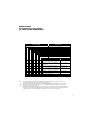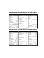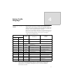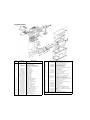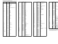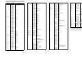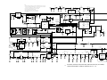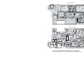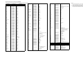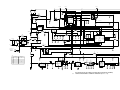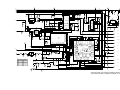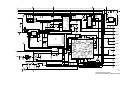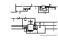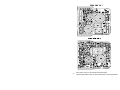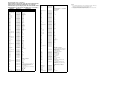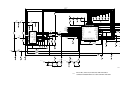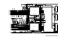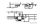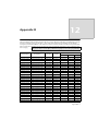
1
HT 1000™, JT 1000®, MT 2000™, MTS 2000™, and MTX Series Handie-Talkie® Portable Radios Service Manual HT 1000™, JT 1000®, MT 2000™, MTS 2000™, and MTX Series Handie-Talkie® Portable Radios Service Manual MOTOROLA, the Stylized M logo, Handie-Talkie, Private-Line, Digital Private-Line, FLASHport, HearClear, HT 1000, JT 1000, MT 2000, MTS 2000, MTX 2000, MTX 838, MTX 8000, and MTX 9000 are registered in the US Patent & Trademark Office. All other product or service names are the property of their respective owners. © 2003, 2001, 1998 by Motorola, Inc. Commercial, Government and Industrial Solutions Sector 8000 W. Sunrise Boulevard Fort Lauderdale, Florida 33322 Printed in U.S.A. 7/03. All Rights Reserved. 6881200C75-B Safety 1 Foreword The information contained in this manual relates to all HT 1000™, JT1000®, MT 2000™, MTS 2000™, and MTX Series Handie-Talkie® portable radios, unless otherwise specified. This manual provides sufficient information to enable qualified service shop technicians to troubleshoot and repair the portable radio to the component level. For details on the operation of the radio or level 1 or 2 maintenance procedures, refer to the applicable manuals, which are available separately. A list of related publications is provided in the section, “Related Publications Available Separately” on page vii. Product Safety and RF Exposure Compliance ! Caution Before using this product, read the operating instructions for safe usage contained in the Product Safety and RF Exposure booklet enclosed with your radio. ATTENTION! This radio is restricted to occupational use only to satisfy FCC RF energy exposure requirements. Before using this product, read the RF energy awareness information and operating instructions in the Product Safety and RF Exposure booklet enclosed with your radio (Motorola Publication part number 6881095C98) to ensure compliance with RF energy exposure limits. For a list of Motorola-approved antennas, batteries, and other accessories, visit the following web site which lists approved accessories: <http://www.motorola.com/cgiss/index.shtml> Manual Revisions Changes which occur after this manual is printed are described in FMRs (Florida Manual Revisions). These FMRs provide complete replacement pages for all added, changed, and deleted items, including pertinent parts list data, schematics, and component layout diagrams. To obtain FMRs, contact the Radio Parts Services Division (refer to “Replacement Parts Ordering” on page 115). Computer Software Copyrights The Motorola products described in this manual may include copyrighted Motorola computer programs stored in semiconductor memories or other media. Laws in the United States and other countries preserve for Motorola certain exclusive rights for copyrighted computer programs, including, but not limited to, the exclusive right to copy or reproduce in any form the copyrighted computer program. Accordingly, any copyrighted Motorola computer programs contained in the Motorola products described in this manual may not be copied, reproduced, modified, reverse-engineered, or distributed in any manner without the express written permission of Motorola. Furthermore, the purchase of Motorola products shall not be deemed to grant either directly or by implication, estoppel, or otherwise, any license under the copyrights, patents or patent applications of Motorola, except for the normal non-exclusive license to use that arises by operation of law in the sale of a product. Document Copyrights No duplication or distribution of this document or any portion thereof shall take place without the express written permission of Motorola. No part of this manual may be reproduced, distributed, or transmitted in any form or by any means, electronic or mechanical, for any purpose without the express written permission of Motorola. Disclaimer The information in this document is carefully examined, and is believed to be entirely reliable. However, no responsibility is assumed for inaccuracies. Furthermore, Motorola reserves the right to make changes to any products herein to improve readability, function, or design. Motorola does not assume any liability arising out of the applications or use of any product or circuit described herein; nor does it cover any license under its patent rights nor the rights of others. Trademarks MOTOROLA and the Stylized M logo are registered in the US Patent & Trademark Office. All other product or service names are the property of their respective owners. © Motorola, Inc. 2003. Contents List of Tables . . . . . . . . . . . . . . . . . . . . . . . . . . . . . . . . . . . . . . . . . . . . . . . . . . . . . . . . . . . . . . . . . . . . vi Related Publications Available Separately . . . . . . . . . . . . . . . . . . . . . . . . . . . . . . . . . . . . . . . . . . . . vii Model Numbering System . . . . . . . . . . . . . . . . . . . . . . . . . . . . . . . . . . . . . . . . . . . . . . . . . . . . . . . . . viii Model Charts, Model Programming, Flashing, and Cloning . . . . . . . . . . . . . . . . . . . . . . . . . . . . . .vii Model Charts General Description . . . . . . . . . . . . . . . . . . . . . . . . . . . . . . . . . . . . . . . . . . . . . . . . . . .vii Programming, Flashing, and Cloning . . . . . . . . . . . . . . . . . . . . . . . . . . . . . . . . . . . . . . . . . . . . . . . . .vii MODEL CHART, Conventional Systems Radios (HT 1000 Models) . . . . . . . . . . . . . . . . . . . . . . . . . viii MODEL CHART, Conventional Systems Radios (JT 1000 and MT 2000 Models) . . . . . . . . . . . . . . . ix MODEL CHART, Private Systems Radios (MTS 2000 Models) . . . . . . . . . . . . . . . . . . . . . . . . . . . . . . .x MODEL CHART, Shared Systems Radios (MTX 838, MTX 8000, MTX•LS, and MTX 9000 Models) . . . . . . . . . . . . . . . . . . . . . . . . . . . . . . . . . . . . . . . . . . . . . . . . . . . . . . . . . . . . . . xi List of Antennas . . . . . . . . . . . . . . . . . . . . . . . . . . . . . . . . . . . . . . . . . . . . . . . . . . . . . . . . . . . . . . . . . xii List of Batteries . . . . . . . . . . . . . . . . . . . . . . . . . . . . . . . . . . . . . . . . . . . . . . . . . . . . . . . . . . . . . . . . . xii Maintenance Specifications for VHF Radios . . . . . . . . . . . . . . . . . . . . . . . . . . . . . . . . . . . . . . . . . . xiii Maintenance Specifications for UHF Radios . . . . . . . . . . . . . . . . . . . . . . . . . . . . . . . . . . . . . . . . . . xiii Maintenance Specifications for 800MHz Radios . . . . . . . . . . . . . . . . . . . . . . . . . . . . . . . . . . . . . . . xiv Maintenance Specifications for 900MHz Radios . . . . . . . . . . . . . . . . . . . . . . . . . . . . . . . . . . . . . . . xiv Glossary . . . . . . . . . . . . . . . . . . . . . . . . . . . . . . . . . . . . . . . . . . . . . . . . . . . . . . . . . . . . . . . . . . . . . . . .xv 1 - Introduction . . . . . . . . . . . . . . . . . . . . . . . . . . . . . . . . . . . . . . . . . . . . . . . . . . . . . . . . . . . . . . . . . . . 1 2 - Test Equipment, Service Aids, and Tools. . . . . . . . . . . . . . . . . . . . . . . . . . . . . . . . . . . . . . . . . . . . . 3 Recommended Test Equipment. . . . . . . . . . . . . . . . . . . . . . . . . . . . . . . . . . . . . . . . . . . . . . . . . . . . . . .3 Service Aids and Recommended Tools . . . . . . . . . . . . . . . . . . . . . . . . . . . . . . . . . . . . . . . . . . . . . . . . .4 Field Programming . . . . . . . . . . . . . . . . . . . . . . . . . . . . . . . . . . . . . . . . . . . . . . . . . . . . . . . . . . . . . . . .4 3 - Transceiver Performance Testing. . . . . . . . . . . . . . . . . . . . . . . . . . . . . . . . . . . . . . . . . . . . . . . . . . . 7 General. . . . . . . . . . . . . . . . . . . . . . . . . . . . . . . . . . . . . . . . . . . . . . . . . . . . . . . . . . . . . . . . . . . . . . . . . .7 Setup . . . . . . . . . . . . . . . . . . . . . . . . . . . . . . . . . . . . . . . . . . . . . . . . . . . . . . . . . . . . . . . . . . . . . . . . . . .7 Test Mode. . . . . . . . . . . . . . . . . . . . . . . . . . . . . . . . . . . . . . . . . . . . . . . . . . . . . . . . . . . . . . . . . . . . . . . .7 4 - Error-Code Displays . . . . . . . . . . . . . . . . . . . . . . . . . . . . . . . . . . . . . . . . . . . . . . . . . . . . . . . . . . . . 15 Power-up Display Codes . . . . . . . . . . . . . . . . . . . . . . . . . . . . . . . . . . . . . . . . . . . . . . . . . . . . . . . . . . .15 Operational Display Codes . . . . . . . . . . . . . . . . . . . . . . . . . . . . . . . . . . . . . . . . . . . . . . . . . . . . . . . . .16 5 - Radio Alignment Procedure . . . . . . . . . . . . . . . . . . . . . . . . . . . . . . . . . . . . . . . . . . . . . . . . . . . . . . 17 General. . . . . . . . . . . . . . . . . . . . . . . . . . . . . . . . . . . . . . . . . . . . . . . . . . . . . . . . . . . . . . . . . . . . . . . . .17 Reference Oscillator Alignment . . . . . . . . . . . . . . . . . . . . . . . . . . . . . . . . . . . . . . . . . . . . . . . . . . . . . .19 i Front-EndPre-Selector VHF/UHF only) . . . . . . . . . . . . . . . . . . . . . . . . . . . . . . . . . . . . . . . . . . . . . . . .20 Rated Audio . . . . . . . . . . . . . . . . . . . . . . . . . . . . . . . . . . . . . . . . . . . . . . . . . . . . . . . . . . . . . . . . . . . . .20 Squelch . . . . . . . . . . . . . . . . . . . . . . . . . . . . . . . . . . . . . . . . . . . . . . . . . . . . . . . . . . . . . . . . . . . . . . . . .21 Transmitter Power . . . . . . . . . . . . . . . . . . . . . . . . . . . . . . . . . . . . . . . . . . . . . . . . . . . . . . . . . . . . . . . .21 Transmit Deviation Balance (Compensation) . . . . . . . . . . . . . . . . . . . . . . . . . . . . . . . . . . . . . . . . . . .22 Transmit Deviation Limit . . . . . . . . . . . . . . . . . . . . . . . . . . . . . . . . . . . . . . . . . . . . . . . . . . . . . . . . . .23 Transmit Deviation Limit Reference . . . . . . . . . . . . . . . . . . . . . . . . . . . . . . . . . . . . . . . . . . . . . . . . . .23 VCO Crossover Frequency . . . . . . . . . . . . . . . . . . . . . . . . . . . . . . . . . . . . . . . . . . . . . . . . . . . . . . . . . .24 Signalling Deviation. . . . . . . . . . . . . . . . . . . . . . . . . . . . . . . . . . . . . . . . . . . . . . . . . . . . . . . . . . . . . . .27 Alignment Procedure Conclusion . . . . . . . . . . . . . . . . . . . . . . . . . . . . . . . . . . . . . . . . . . . . . . . . . . . .28 6 - Disassembly and Reassembly . . . . . . . . . . . . . . . . . . . . . . . . . . . . . . . . . . . . . . . . . . . . . . . . . . . . .29 General . . . . . . . . . . . . . . . . . . . . . . . . . . . . . . . . . . . . . . . . . . . . . . . . . . . . . . . . . . . . . . . . . . . . . . . . .30 Disassembly to Board Level . . . . . . . . . . . . . . . . . . . . . . . . . . . . . . . . . . . . . . . . . . . . . . . . . . . . . . . . .30 Disassembly of Control Top. . . . . . . . . . . . . . . . . . . . . . . . . . . . . . . . . . . . . . . . . . . . . . . . . . . . . . . . .34 Disassembly of Front Cover Assembly. . . . . . . . . . . . . . . . . . . . . . . . . . . . . . . . . . . . . . . . . . . . . . . . .35 Reassembly . . . . . . . . . . . . . . . . . . . . . . . . . . . . . . . . . . . . . . . . . . . . . . . . . . . . . . . . . . . . . . . . . . . . . .36 7 - Maintenance . . . . . . . . . . . . . . . . . . . . . . . . . . . . . . . . . . . . . . . . . . . . . . . . . . . . . . . . . . . . . . . . . .41 Introduction . . . . . . . . . . . . . . . . . . . . . . . . . . . . . . . . . . . . . . . . . . . . . . . . . . . . . . . . . . . . . . . . . . . . .41 Preventive Maintenance . . . . . . . . . . . . . . . . . . . . . . . . . . . . . . . . . . . . . . . . . . . . . . . . . . . . . . . . . . .41 Safe Handling of CMOS Devices . . . . . . . . . . . . . . . . . . . . . . . . . . . . . . . . . . . . . . . . . . . . . . . . . . . . .42 Repair Procedures and Techniques . . . . . . . . . . . . . . . . . . . . . . . . . . . . . . . . . . . . . . . . . . . . . . . . . . .42 8 - Exploded Views. . . . . . . . . . . . . . . . . . . . . . . . . . . . . . . . . . . . . . . . . . . . . . . . . . . . . . . . . . . . . . . .51 Basic Radios and Basic Radios with Option Mate Optional Front Cover . . . . . . . . . . . . . . . . . . . . . .52 Top-Display Radios . . . . . . . . . . . . . . . . . . . . . . . . . . . . . . . . . . . . . . . . . . . . . . . . . . . . . . . . . . . . . . .53 Keypad Radios . . . . . . . . . . . . . . . . . . . . . . . . . . . . . . . . . . . . . . . . . . . . . . . . . . . . . . . . . . . . . . . . . . .54 Uni-board Radios . . . . . . . . . . . . . . . . . . . . . . . . . . . . . . . . . . . . . . . . . . . . . . . . . . . . . . . . . . . . . . . . .55 9 - Component Location Diagrams, Parts Lists, and Schematic Diagrams. . . . . . . . . . . . . . . . . . . .57 Introduction . . . . . . . . . . . . . . . . . . . . . . . . . . . . . . . . . . . . . . . . . . . . . . . . . . . . . . . . . . . . . . . . . . . . .57 NUD7091B, NUD7092B, NUD/PMUD7095B, AND NUD7096B VHF (136-178MHz) TRANSCEIVER BOARDS’ PARTS LIST AND COMPONENT LOCATION DIAGRAMS . . . . . . . . . . . . . . . . . . . . . . . .62 Electrical Parts List, VHF Transceivers NUD7091B, NUD7092B, NUD/PMUD7095B, NUD7096B. . .63 NUD7091B, NUD7092B, NUD/PMUD7095B, AND NUD7096B VHF (136-178MHz) TRANSCEIVER BOARDS’ SCHEMATIC DIAGRAM (Sheet 1 of 2) . . . . . . . . . . . . . . . . . . . . . . . . . . . . . . . . . . . . . . .64 NUD7091B, NUD7092B, NUD/PMUD7095B, AND NUD7096B VHF (136-178 MHz) TRANSCEIVER BOARDS’ SCHEMATIC DIAGRAM (Sheet 2 of 2) . . . . . . . . . . . . . . . . . . . . . . . . . . . . . . . . . . . . . . .65 NUE7265B, NUE7266B, NUE/PMUE7272B, AND NUE7274B UHF (403-470MHz) TRANSCEIVER BOARDS’ PARTS LIST AND COMPONENT LOCATION DIAGRAMS . . . . . . . . . . . . . . . . . . . . . . . .66 Electrical Parts List, UHF Transceivers (403-470MHz) NUE7265B, NUE7266B, NUE/PMUE7272B, NUE7274B . . . . . . . . . . . . . . . . . . . . . . . . . . . . . . . . . . . . . . . . . . . . . . . . . . . . . . . . . . . . . . . . . . . . .67 NUE7265B, NUE7266B, NUE/PMUE7272B, AND NUE7274B UHF (403-470MHz) TRANSCEIVER BOARDS’ SCHEMATIC DIAGRAM (Sheet 1 of 2) . . . . . . . . . . . . . . . . . . . . . . . . . . . . . . . . . . . . . . .68 ii NUE7265B, NUE7266B, NUE/PMUE7272B, AND NUE7274B UHF (403-470MHz) TRANSCEIVER BOARDS’ SCHEMATIC DIAGRAM (Sheet 2 of 2) . . . . . . . . . . . . . . . . . . . . . . . . . . . . . . . . . . . . . . .69 NUE7267B, NUE7268B, NUE/PMUE7273B, AND NUE7275B UHF (450-520MHz) TRANSCEIVER BOARDS’ PARTS LIST AND COMPONENT LOCATION DIAGRAMS . . . . . . . . . . . . . . . . . . . . . . . .70 Electrical Parts List, UHF Transceivers (450–520MHz) NUE7267B, NUE7268B, NUE/PMUE7273B, NUE7275B . . . . . . . . . . . . . . . . . . . . . . . . . . . . . . . . . . . . . . . . . . . . . . . . . . . . . . . . . . . . . . . . . . . . .71 NUE7267B, NUE7268B, NUE/PMUE7273B, AND NUE7275B UHF (450-520MHz) TRANSCEIVER BOARDS’ SCHEMATIC DIAGRAM (Sheet 1 of 2) . . . . . . . . . . . . . . . . . . . . . . . . . . . . . . . . . . . . . . .72 NUE7267B, NUE7268B, NUE/PMUE7273B, AND NUE7275B UHF (450-520MHz) TRANSCEIVER BOARDS’ SCHEMATIC DIAGRAM (Sheet 2 of 2) . . . . . . . . . . . . . . . . . . . . . . . . . . . . . . . . . . . . . . .73 NUF6410B/C, NUF6498B/C, NUF6500B/C AND NUF6501C (800MHz) TRANSCEIVER BOARDS’ PARTS LIST AND COMPONENT LOCATION DIAGRAMS . . . . . . . . . . . . . . . . . . . . . . . .74 Electrical Parts List, Transceivers (800MHz) NUF6410B/C, NUF6498B/C, NUF6500B/C AND NUF6501C. . . . . . . . . . . . . . . . . . . . . . . . . . . . . . . . . . . . . . . . . . . . . . . . . . . . . . . . . . . . . . . . . . . . .75 NUF6410B/C, NUF6498B/C, NUF6500B/C AND NUF6501C (800MHz) TRANSCEIVER BOARDS’ SCHEMATIC DIAGRAM (Sheet 1 of 2) . . . . . . . . . . . . . . . . . . . . . . . . . . . . . . . . . . . . . . . . . . . . . . .76 NUF6410B/C, NUF6498B/C, NUF6500B/C AND NUF6501C (800MHz) TRANSCEIVER BOARDS’ SCHEMATIC DIAGRAM (Sheet 2 of 2) . . . . . . . . . . . . . . . . . . . . . . . . . . . . . . . . . . . . . . . . . . . . . . .77 NUF/PMUF6500D, NUF/PMUF6533A AND NUF/PMUF6410D (800MHz) TRANSCEIVER BOARD PARTS LIST AND COMPONENT LOCATION DIAGRAMS . . . . . . . . . . . . . . . . . . . . . . . . . . . . . . . .78 Electrical Parts List, Transceiver (800MHz) NUF/PMUF6500D, NUF/PMUF6533A AND NUF/ PMUF6410D . . . . . . . . . . . . . . . . . . . . . . . . . . . . . . . . . . . . . . . . . . . . . . . . . . . . . . . . . . . . . . . . . . .79 NUF/PMUF6500D, NUF/PMUF6533A AND NUF/PMUF6410D (800MHz) TRANSCEIVER BOARDS’ SCHEMATIC DIAGRAM (Sheet 1 of 2) . . . . . . . . . . . . . . . . . . . . . . . . . . . . . . . . . . . . . . . . . . . . . . .80 NUF/PMUF6500D, NUF/PMUF6533A AND NUF/PMUF6410D (800MHz) TRANSCEIVER BOARDS’ SCHEMATIC DIAGRAM (Sheet 2 of 2) . . . . . . . . . . . . . . . . . . . . . . . . . . . . . . . . . . . . . . . . . . . . . . .81 NUF6499B/C AND NUF6502B/C (900MHz) TRANSCEIVER BOARDS’ PARTS LIST AND COMPONENT LOCATION DIAGRAMS . . . . . . . . . . . . . . . . . . . . . . . . . . . . . . . . . . . . . . . . . . . . . .82 Electrical Parts List, Transceivers (900MHz) NUF6499B/C AND NUF6502B/C . . . . . . . . . . . . . . . . .83 NUF6499B/C AND NUF6502B/C (900MHz) TRANSCEIVER BOARDS’ SCHEMATIC DIAGRAM (Sheet 1 of 2) . . . . . . . . . . . . . . . . . . . . . . . . . . . . . . . . . . . . . . . . . . . . . . . . . . . . . . . . . . . . . . . . . . .84 NUF6499B/C AND NUF6502B/C (900MHz) TRANSCEIVER BOARDS’ SCHEMATIC DIAGRAM (Sheet 2 of 2) . . . . . . . . . . . . . . . . . . . . . . . . . . . . . . . . . . . . . . . . . . . . . . . . . . . . . . . . . . . . . . . . . . .85 NUF/PMUF6499D (900MHz) TRANSCEIVER BOARD PARTS LIST AND COMPONENT LOCATION DIAGRAMS . . . . . . . . . . . . . . . . . . . . . . . . . . . . . . . . . . . . . . . . . . . . . . . . . . . . . . . . . . . . . . . . . . . .86 Electrical Parts List, Transceiver (900MHz) NUF/PMUF6499D . . . . . . . . . . . . . . . . . . . . . . . . . . . . . .87 NUF/PMUF6499D (900MHz) TRANSCEIVER BOARDS’ SCHEMATIC DIAGRAM (Sheet 1 of 2) . . . .88 NUF/PMUF6499D (900MHz) TRANSCEIVER BOARDS’ SCHEMATIC DIAGRAM (Sheet 2 of 2) . . . .89 NCN6145A/C, NCN6146A, NTN7089C, NCN6129C, NCN6138A, NCN6140A/B, NCN6141A, NCN/PMCN6140C CONTROLLER BOARDS’ PARTS LIST AND COMPONENT LOCATION DIAGRAMS . . . . . . . . . . . . . . . . . . . . . . . . . . . . . . . . . . . . . . . . . . . . . . . . . . . . . . . . . . . . . . . . . . . .90 Electrical Parts List, Controller: NCN6129C And NCN6138A (all HT 1000 Models) NCN6140A/B (VHF HT 1000 Models) NCN6141A (UHF HT 1000 Models) NCN/PMCN6140C (all HT 1000 Models) NCN6145A/C (800MHz HT 1000 Models) NTN7089C And NCN6146A (JT 1000 Models) . . . . . . . . . . . . . . . . . . . . . . . . . . . . . . . . . . . . . . . . . . . . . . . . . . . . . . . . . . . . . . . .91 iii NCN6129C, NCN6138A, NCN6140A/B, NCN/PMCN6140C, NCN6141A, NCN6145A/C, NCN6146A, NTN7089C AND PMCN6140C CONTROLLER BOARD ANALOG SECTION SCHEMATIC DIAGRAM . . . . . . . . . . . . . . . . . . . . . . . . . . . . . . . . . . . . . . . . . . . . . . . . . . . . . . . . . .92 NCN6129C, NCN6138A, NCN6140A/B, NCN/PMCN6140C, NCN6141A, NCN6145A/C, NCN6146A, NTN7089C CONTROLLER BOARD DIGITAL SECTION SCHEMATIC DIAGRAM. . . .93 NCN6129C, NCN6138A, NCN6140A/B, NCN/PMCN6140C, NCN6141A, NCN6145A/C, NCN6146A, NTN7089C AND PMCN6140C CONTROLLER BOARD TOP-LEVEL SCHEMATIC . . .94 NCN6129C, NCN6138A, NCN6140A/B, NCN/PMCN6140C, NCN6141A, NCN6145A/C, NCN6146A, NTN7089C CONTROLLER BOARD POWER SECTION SCHEMATIC DIAGRAM . . . .95 NCN6147A/B, NCN6150A/B, NTN7091D, NTN7620E, PMCN6147B AND PMCN6150B CONTROLLER BOARD’ PARTS LIST AND COMPONENT LOCATION DIAGRAM . . . . . . . . . . . . .96 Electrical Parts List, Controllers NCN6147A/B, NCN6150A/B, NTN7091D, NTN7620E, PMCN6147B, PMCN6150B . . . . . . . . . . . . . . . . . . . . . . . . . . . . . . . . . . . . . . . . . . . . . . . . . . . . . . . .97 NCN6147A/B, NCN6150A/B, NTN7091D, NTN7620E, PMCN6147B AND PMCN6150B CONTROLLER BOARD ANALOG SECTION SCHEMATIC DIAGRAM . . . . . . . . . . . . . . . . . . . . . . .98 NCN6147A/B, NCN6150A/B, NTN7091D, NTN7620E, PMCN6147B AND PMCN6150B CONTROLLER BOARD DIGITAL SECTION SCHEMATIC DIAGRAM . . . . . . . . . . . . . . . . . . . . . . .99 NCN6147A/B, NCN6150A/B, NTN7091D, NTN7620E, PMCN6147B AND PMCN6150B CONTROLLER BOARD TOP-LEVEL SCHEMATIC . . . . . . . . . . . . . . . . . . . . . . . . . . . . . . . . . . . . .100 NCN6147A/B, NCN6150A/B, NTN7091D, NTN7620E, PMCN6147B AND PMCN6150B CONTROLLER BOARD POWER SECTION SCHEMATIC DIAGRAM . . . . . . . . . . . . . . . . . . . . . . .101 NTN7512D/E, NTN7513E, NTN7857D/E AND NTN7858D/E CONTROLLER BOARDS’ PARTS LIST AND COMPONENT LOCATION DIAGRAMS . . . . . . . . . . . . . . . . . . . . . . . . . . . . . . .102 Electrical Parts List, Controllers NTN7512D/E Front Display VHF, UHF and 800MHz Radios NTN7513E Front Display 900MHz Hear Clear Radios NTN7857D/E Top/No Display VHF, UHF and 800MHz Radios NTN7858D/E Top/No Display 900MHz Hear Clear Radios . . . . . . . . .103 NTN7512D/E, NTN7513E, NTN7857D/E AND NTN7858D/E CONTROLLER BOARD ANALOG SECTION SCHEMATIC DIAGRAM . . . . . . . . . . . . . . . . . . . . . . . . . . . . . . . . . . . . . . . . . . . . . . . . .104 NTN7512D/E, NTN7513E, NTN7857D/E AND NTN7858D/E CONTROLLER BOARD DIGITAL SECTION SCHEMATIC DIAGRAM . . . . . . . . . . . . . . . . . . . . . . . . . . . . . . . . . . . . . . . . . . . . . . . . .105 NTN7512D/E, NTN7513E, NTN7857D/E AND NTN7858D/E CONTROLLER BOARD TOP-LEVEL SCHEMATIC . . . . . . . . . . . . . . . . . . . . . . . . . . . . . . . . . . . . . . . . . . . . . . . . . . . . . . . . . . . . . . . . . .106 NTN7512D/E, NTN7513E, NTN7857D/E AND NTN7858D/E CONTROLLER BOARD POWER SECTION SCHEMATIC DIAGRAM . . . . . . . . . . . . . . . . . . . . . . . . . . . . . . . . . . . . . . . . . . . . . . . . .107 NCN6106C, NCN/PMCN6153A/B, AND NCN/PMCN6176A CONTROLLER BOARDS’ PARTS LIST AND COMPONENT LAYOUT DIAGRAMS . . . . . . . . . . . . . . . . . . . . . . . . . . . . . . . . . . . . . . .108 Electrical Parts List, Controllers NCN6106C, NCN/PMCN6153A/B, NCN/PMCN6176A. . . . . . . . .109 NCN6106C , NCN/PMCN6153A/B, NCN/PMCN6176A CONTROLLER BOARD ANALOG SECTION SCHEMATIC DIAGRAM . . . . . . . . . . . . . . . . . . . . . . . . . . . . . . . . . . . . . . . . . . . . . . . . .110 NCN6106C, NCN/PMCN6153A/B AND NCN/PMCN6176A CONTROLLER BOARD DIGITAL SECTION SCHEMATIC DIAGRAM . . . . . . . . . . . . . . . . . . . . . . . . . . . . . . . . . . . . . . . . . . . . . . . . .111 NCN6106C AND NCN/PMCN6153A/B AND NCN/PMCN6176A CONTROLLER BOARD TOP-LEVEL SCHEMATIC . . . . . . . . . . . . . . . . . . . . . . . . . . . . . . . . . . . . . . . . . . . . . . . . . . . . . . . . . . . . . . . . . .112 NCN6106C, NCN/PMCN6153A/B AND NCN/PMCN6176A CONTROLLER BOARD POWER SECTION SCHEMATIC DIAGRAM . . . . . . . . . . . . . . . . . . . . . . . . . . . . . . . . . . . . . . . . . . . . . . . . .113 FRONT COVER DISPLAY FLEX AND CONTROLS FLEX SCHEMATIC DIAGRAMS . . . . . . . . . . . . .114 iv 10 - Replacement Parts Ordering . . . . . . . . . . . . . . . . . . . . . . . . . . . . . . . . . . . . . . . . . . . . . . . . . . . 115 Introduction. . . . . . . . . . . . . . . . . . . . . . . . . . . . . . . . . . . . . . . . . . . . . . . . . . . . . . . . . . . . . . . . . . . .115 Motorola Online . . . . . . . . . . . . . . . . . . . . . . . . . . . . . . . . . . . . . . . . . . . . . . . . . . . . . . . . . . . . . . . .115 Mail Orders . . . . . . . . . . . . . . . . . . . . . . . . . . . . . . . . . . . . . . . . . . . . . . . . . . . . . . . . . . . . . . . . . . . .115 Telephone Orders. . . . . . . . . . . . . . . . . . . . . . . . . . . . . . . . . . . . . . . . . . . . . . . . . . . . . . . . . . . . . . . .116 FAX Orders. . . . . . . . . . . . . . . . . . . . . . . . . . . . . . . . . . . . . . . . . . . . . . . . . . . . . . . . . . . . . . . . . . . . .116 Parts Identification . . . . . . . . . . . . . . . . . . . . . . . . . . . . . . . . . . . . . . . . . . . . . . . . . . . . . . . . . . . . . .116 Product Customer Service . . . . . . . . . . . . . . . . . . . . . . . . . . . . . . . . . . . . . . . . . . . . . . . . . . . . . . . . .116 11 - Appendix A . . . . . . . . . . . . . . . . . . . . . . . . . . . . . . . . . . . . . . . . . . . . . . . . . . . . . . . . Appendix A-1 12 - Appendix B . . . . . . . . . . . . . . . . . . . . . . . . . . . . . . . . . . . . . . . . . . . . . . . . . . . . . . . . Appendix B-1 v List of Tables Table 1 - Recommended Test Equipment . . . . . . . . . . . . . . . . . . . . . . . . . . . . . . . . . . . . . . . . . . . . . 3 Table 2 - Service Aids . . . . . . . . . . . . . . . . . . . . . . . . . . . . . . . . . . . . . . . . . . . . . . . . . . . . . . . . . . . . . 5 Table 3 - Recommended Service Tools . . . . . . . . . . . . . . . . . . . . . . . . . . . . . . . . . . . . . . . . . . . . . . . 6 Table 4 - Equipment Initial Control Settings . . . . . . . . . . . . . . . . . . . . . . . . . . . . . . . . . . . . . . . . . . 7 Table 5 - Test Environments, HT 1000/JT 1000 Radios . . . . . . . . . . . . . . . . . . . . . . . . . . . . . . . . . . 8 Table 6 - Test Frequencies, HT 1000 / JT 1000 . . . . . . . . . . . . . . . . . . . . . . . . . . . . . . . . . . . . . . . . . 9 Table 7 - Test Environments, MT 2000, MTS 2000, and MTX Series Radios . . . . . . . . . . . . . . . . . 12 Table 8 - Test Frequencies, MT 2000, MTS 2000, and MTX Series Radios . . . . . . . . . . . . . . . . . . . 12 Table 9 - Receiver Performance Checks. . . . . . . . . . . . . . . . . . . . . . . . . . . . . . . . . . . . . . . . . . . . . . 13 Table 10 - Transmitter Performance Checks . . . . . . . . . . . . . . . . . . . . . . . . . . . . . . . . . . . . . . . . . . . 14 Table 11 - Power-up Display Codes. . . . . . . . . . . . . . . . . . . . . . . . . . . . . . . . . . . . . . . . . . . . . . . . . . 15 Table 12 - Operational Display Codes. . . . . . . . . . . . . . . . . . . . . . . . . . . . . . . . . . . . . . . . . . . . . . . . 16 Table 13 - Reference Oscillator Alignment . . . . . . . . . . . . . . . . . . . . . . . . . . . . . . . . . . . . . . . . . . . . 19 Table 14 - Standard Test Modulation (1 kHz Tone) . . . . . . . . . . . . . . . . . . . . . . . . . . . . . . . . . . . . . 20 Table 15 - Transmit Power Setting . . . . . . . . . . . . . . . . . . . . . . . . . . . . . . . . . . . . . . . . . . . . . . . . . . 22 Table 16 - Transmit Deviation Limit. . . . . . . . . . . . . . . . . . . . . . . . . . . . . . . . . . . . . . . . . . . . . . . . . 23 Table 17 - Transmit Deviation Limit Reference . . . . . . . . . . . . . . . . . . . . . . . . . . . . . . . . . . . . . . . . 24 Table 18 - Signalling Deviation . . . . . . . . . . . . . . . . . . . . . . . . . . . . . . . . . . . . . . . . . . . . . . . . . . . . . 28 Appendix A Table 1 - MTS 2000 Single Key Secure Module I/O Definition . . . . . . . . . . . Appendix A-2 Appendix A Table 2 - Key Variable Loader . . . . . . . . . . . . . . . . . . . . . . . . . . . . . . . . . . . . . Appendix A-4 Appendix A Table 3 - Secure Deviation . . . . . . . . . . . . . . . . . . . . . . . . . . . . . . . . . . . . . . . Appendix A-7 Appendix A Table 4 - RSS Secure Parameters . . . . . . . . . . . . . . . . . . . . . . . . . . . . . . . . . . Appendix A-10 Appendix B Table 1 - HT 1000 Models. . . . . . . . . . . . . . . . . . . . . . . . . . . . . . . . . . . . . . . . Appendix B-1 Appendix B Table 2 - JT 1000 Models . . . . . . . . . . . . . . . . . . . . . . . . . . . . . . . . . . . . . . . . Appendix B-3 Appendix B Table 3 - MT 2000 Models . . . . . . . . . . . . . . . . . . . . . . . . . . . . . . . . . . . . . . . Appendix B-4 Appendix B Table 4 - MTS 2000 Models . . . . . . . . . . . . . . . . . . . . . . . . . . . . . . . . . . . . . . Appendix B-7 Appendix B Table 5 - MTX Series Models . . . . . . . . . . . . . . . . . . . . . . . . . . . . . . . . . . . . Appendix B-13 vi Related Publications Available Separately Service Manual (earliest version radios; first issue- 4/92) . . . . . . . . . . . . . . . . . . . . . . . . . . . 68P81200C20 Service Manual (early version radios; first issue- 4/93) . . . . . . . . . . . . . . . . . . . . . . . . . . . . . 68P81200C25 Service Manual (later version radios; first issue- 7/94) . . . . . . . . . . . . . . . . . . . . . . . . . . . . . 68P81200C40 Service Manual (this publication; present version radios; first issue- 3/98) . . . . . . . . . . . . . 68P81200C75 includes: • all servicing information • assembly / disassembly • maintenance Theory Manual . . . . . . . . . . . . . . . . . . . . . . . . . . . . . . . . . . . . . . . . . . . . . . . . . . . . . . . . . . . 68P81200C15 includes: • theory of operation • troubleshooting information and troubleshooting charts Operating Instructions • HT 1000 A Model Portable Radios . . . . . . . . . . . . . . . . . . . . . . . . . . . . . . . . . . . . . . . 68P81071C70 • HT 1000 B Model and later Portable Radios . . . . . . . . . . . . . . . . . . . . . . . . . . . . . . . . 68P81079C50 • JT 1000 Portable Radios . . . . . . . . . . . . . . . . . . . . . . . . . . . . . . . . . . . . . . . . . . . . . . . 68P81078C45 • JT 1000 Portable Radios Front Panel Programming Instructions . . . . . . . . . . . . . . . . 68P81081C30 • MT 2000 Portable Radios . . . . . . . . . . . . . . . . . . . . . . . . . . . . . . . . . . . . . . . . . . . . . . 68P81076C65 • MTS 2000 I Portable Radios . . . . . . . . . . . . . . . . . . . . . . . . . . . . . . . . . . . . . . . . . . . . 68P81072C15 • MTS 2000 II and III Portable Radios . . . . . . . . . . . . . . . . . . . . . . . . . . . . . . . . . . . . . . 68P81072C45 • MTX Series Model B3 Privacy Plus Portable Radios . . . . . . . . . . . . . . . . . . . . . . . . . . 68P81072C10 • MTX Series Model B4 Privacy Plus Portable Radios . . . . . . . . . . . . . . . . . . . . . . . . . . 68P81073C60 • MTX Series Model B5 and B7 Privacy Plus Portable Radios . . . . . . . . . . . . . . . . . . . . 68P81072C40 • MTX•LS Trunked Portable Radios. . . . . . . . . . . . . . . . . . . . . . . . . . . . . . . . . . . . . . . . 68P81083C35 Mobile Vehicular Adapter (MTVA) Operating Instructions. . . . . . . . . . . . . . . . . . . . . . . . . . 68P81075C85 Mobile Vehicular Adapter (MTVA) Installation Instructions . . . . . . . . . . . . . . . . . . . . . . . . 68P81075C90 Mobile Vehicular Adapter (MTVA) Service Manual. . . . . . . . . . . . . . . . . . . . . . . . . . . . . . . . 68P81075C95 Option•Mate, HT 1000 Analog Voice Security; Installation/ Programming/Troubleshooting Manual . . . . . . . . . . . . . . . . . . . . . . . . . . . . . . . . . . . . . . . . 68P81084C35 Option•Mate, HT 1000 Analog Voice Security Operating Instructions . . . . . . . . . . . . . . . . 68P81084C36 Option•Mate, HT 1000 Analog Voice Security Service Help Card . . . . . . . . . . . . . . . . . . . . 68P81084C37 Refer to Chapter 10 for ordering information. vii Model Numbering System Typical Model Number: H Position: 1 0 2 1 3 K 4 D 5 H = Hand-Held Portable P 8 W 9 1 10 B 11 N 12 S 13 P 14 0 15 1 16 Position 12 Unique Model Variations C = Cenelec N = Standard Package Positions 2 & 3 - Model Series 336 to 410MHz 403 to 437MHz 438 to 482MHz 470 to 520MHz Product Specific 806 to 870MHz 825 to 870MHz 896 to 941MHz 1.0 to 1.6GHz 1.5 to 2.0GHz Values given represent range only; they are not absolute. Position 5 - Power Level A = 0 to 0.7 Watts B = 0.7 to 0.9 Watts C = 1.0 to 3.9 Watts D = 4.0 to 5.0 Watts E = 5.1 to 6.0 Watts F = 6.1 to 10 Watts Position 6 - Physical Packages A = RF Modem Operation B = Receiver Only C = Standard Control; No Display D = Standard Control; With Top Display E = Limited Keypad; No Display F = Limited Keypad; With Front Display G = Full Keypad; No Display H = Full Keypad; With Front Display J = Limited Controls; No Display K = Limited Controls; Basic Display L = Limited Controls; Limited Display M = Rotary Controls; Standard Display N = Enhanced Controls; Enhanced Display P = Low Profile; No Display Q = Low Profile; Basic Display R = Low Profile; Basic Display, Full Keypad Position 7 - Channel Spacing 1 = 5kHz 5 = 15kHz 2 = 6.25kHz 6 = 20/25kHz 3 = 10kHz 7 = 30kHz 4 = 12.5kHz 9 = Variable/Programmable viii 9 7 Positions 13 - 16 “SP” Model Suffix Position 1 - Type of Unit Position 4 - Frequency Band A = Less than 29.7MHz P = B = 29.7 to 35.99MHz Q= C = 36 to 41.99MHz R= D = 42 to 50MHz S = F = 66 to 80MHz T = G = 74 to 90MHz U= H = Product Specific V = J = 136 to 162MHz W= K = 146 to 178MHz Y = L = 174 to 210MHz Z = M = 190 to 235MHz D 6 Position 11 - Version Version Letter (Alpha) - Major Change Position 10 - Feature Level 1 = Basic 6 = Standard Plus 2 = Limited Package 7 = Expanded Package 3 = Limited Plus 8 = Expanded Plus 4 = Intermediate 9 = Full Feature/ 5 = Standard Package Programmable Position 9 - Primary System Type A = Conventional B = Privacy Plus® C = Clear SMARTNET™ D = Advanced Conventional Stat-Alert™ E = Enhanced Privacy Plus® F = Nauganet 888 Series G = Japan Specialized Mobile Radio (JSMR) H = Multi-Channel Access (MCA) J = CoveragePLUS™ K = MPT1327* - Public L = MPT1327* - Private M = Radiocom N = Tone Signalling P = Binary Signalling Q = Phonenet® W = Programmable X = Secure Conventional Y = Secure SMARTNET™ * MPT = Ministry of Posts and Telecommunications Position 8 - Primary Operation A = Conventinal/Simplex B = Conventional/Duplex C = Trunked Twin Type D = Dual Mode Trunked E = Dual Mode Trunked/Duplex F = Trunked Type I G = Trunked Type II H = FDMA* Digital Dual Mode J = TDMA** Digital Dual Mode K = Single Sideband L = Global Positioning Satellite Capable M = Amplitude Companded Sideband (ACSB) P = Programmable * FDMA = Frequency Division Multiple Access ** TDMA = Time Division Multiple Access Model Charts Model Programming, Flashing, and Cloning Model Charts General Description Four model charts cover the three families of radios discussed in this publication: Conventional Systems Radios, HT 1000 Conventional Systems Radios, JT 1000 and MT 2000 Private Systems Radios Shared Systems Radios Each model chart lists the model number and its description, and the three main radio components: the transceiver board, the controller board, and the front cover. A single model may be built using alternate controller boards and alternate transceiver boards. The model charts will list all alternate controllers and all alternate transceivers for any one particular model. Other model components are referenced in electrical parts lists and exploded view parts lists located toward the rear of the manual. To determine which controller and transceiver is in a radio, that radio must be opened and physically examined. Identification kit number labels are attached to the controller board and to the transceiver board. Programming, Flashing, and Cloning All HT 1000, JT 1000, MT 2000, MTS 2000, and MTX Series Radios covered in this manual are clonable. The JT 1000 Model Radios are also front-panel programmable, and the MTS 2000 Series Radios are “flashable.” The following cloning information applies only to HT 1000 Model Radios. HT 1000 Model Radios: VHF DN models cannot be cloned to AN, BN, or CN models. Any DN model can be cloned from like CN or DN models. Prior to cloning any AN or BN model into a like CN or DN model, a code plug fix must be performed on the AN or BN model. Failure to do so could seriously degrade the scan and battery-saver capabilities of the CN or DN model radio. For code plug-fix information, order Service Repair Notice, SRN-1218. Note: Cloning any AN model into a like CN or DN model will remove the TEST MODE capability. vii MODEL CHART Conventional Systems Radios (HT 1000 Models) MODEL NUMBER H01KDC9AA1DN H01KDC9AA3DN H01RDC9AA1DN H01RDC9AA3DN H01SDC9AA1DN H01SDC9AA3DN H01UCC6AA3DN DESCRIPTION VHF, 2F, 5- to 1-Watt VHF, 16F, 5- to 1-Watt UHF B1, 2F, 4- to 1-Watt UHF B1, 16F, 4- to 1-Watt UHF B2, 2F, 4- to 1-Watt UHF B2, 16F, 4- to 1-Watt 800MHz, 16F, 3-Watt ITEM NO. A A A A A A A A A A A A A A B B B B B B B B B B B B B B X X X X X X X X X X A B X * viii = = = = DESCRIPTION Transceiver Board Transceiver Board Transceiver Board Transceiver Board Transceiver Board Transceiver Board Transceiver Board NCN6129C / NCN6129D / NCN6129E / NCN6129F / Controller Board * NCN6129G /NCN6138A / NCN6138B / NCN6140A / NCN6140B B B B B Note: NUD7085E / NUD7085F / NUD7091A / NUD7091B / NUD7095B / PMUD7095B NUD7070E / NUD7070F / NUD7092A / NUD7092B NUD7095B / PMUD7095B NUE7240D / NUE7240E / NUE7265A / NUE7265B NUE7272B / PMUE7272B NUE7231C / NUE7231D / NUE7266A / NUE7266B NUE7272B / PMUE7272B NUE7241D / NUE7241E / NUE7267A / NUE7267B NUE7273B / PMUE7273B NUE7232C / NUE7232D / NUE7268A / NUE7268B NUE7273B / PMUE7273B NUF6394B / NUF6497A / NUF6497B / NUF6500D / PMUF6500D NCN6129C / NCN6141A / NCN6141B / NCN6141C NCN6129C / NCN6145A / NCN6145B / NCN6145C NCN6140C/ PMCN6140C NTN7151B / NTN7151C NTN7156A / NTN7156B Controller Board * Controller Board * Controller Board * Front Cover Front Cover This model chart lists the model numbers and their respective major components of all conventional systems radios covered in this publication. Alternate transceiver board supplied, see “Model Charts General Description” (this section). Alternate controller board supplied, see “Model Charts General Description” (this section). One item is supplied per radio. The radio model number is required when placing an order for the controller board. The model number can be found on the FCC Label on the back of the radio. Refer to Replacement Parts Ordering, Section 10 of this manual for instructions on how to place an order. MODEL CHART Conventional Systems Radios (JT 1000 and MT 2000 Models) MODEL NUMBER DESCRIPTION H01KDH9PA3AN H01RDH9PA3AN H01SDH9PA3AN H01KDD9AA4AN H01KDH9AA7AN H01RDD9AA4AN H01RDH9AA7AN H01SDD9AA4AN H01SDH9AA7AN H01UCD6AA4AN H01UCH6AA7AN JT 1000, VHF, 16CH, Front Display JT 1000, UHF B1, 16CH, Front Display JT 1000, UHF B2, 16CH, Front Display MT 2000, VHF, 16F, 5- to 1-Watt, Top Display MT 2000, VHF, 16CH, 5- to 1-Watt, Front Display MT 2000, UHF B1, 16F, 4- to 1-Watt, Top Display MT 2000, UHF B1, 16CH, 4- to 1-Watt, Front Display MT 2000, UHF B2, 16F, 4- to 1-Watt, Top Display MT 2000, UHF B2, 16CH, 4- to 1-Watt, Front Display MT 2000, 800MHz, 16F, 4- to 1-Watt, Top Display MT 2000, 800MHz, 16CH, 4- to 1-Watt, Front Display ITEM NO. A A A A A A A A A A A A A A A A A A A A A A A A A A A B B B B B B B B B B B B B B B B B B B X X X X X X X X X X X Note: A B X * = = = = DESCRIPTION NUD7070E / NUD7070F / NUD7095A / NUD7095B / NUD7092B / PMUD7095B NUE7231C / NUE7231D / NUE7272A / NUE7272B / NUE7272C / NUE7272D / PMUE7272B Transceiver Board NUE7232C / NUE7232D / NUE7273A / NUE7273B / NUE7273C / PMUE7273B NUF6394B / NUF6498A / NUF6498B / NUF6498C / NUF6500A / NUF6500B / NUF6500C / NUF6500D / PMUF6500D Transceiver Board NTN7089C / NTN7089D / NCN6146A NTN7091D / NTN7091E / NCN6147A / NCN6147B / PMCN6147B NTN7152A / NTN7152B NTN7154A / NTN7154B Transceiver Board Transceiver Board Controller Board * Controller Board * Front Cover Front Cover This model chart lists the model numbers and their respective major components of all conventional systems radios covered in this publication. Alternate transceiver board supplied, see “Model Charts General Description” (this section). Alternate controller board supplied, see “Model Charts General Description” (this section). One item is supplied per radio. The radio model number is required when placing an order for the controller board. The model number can be found on the FCC Label on the back of the radio. Refer to Replacement Parts Ordering, Section 10 of this manual for instructions on how to place an order. ix MODEL CHART Private Systems Radios (MTS 2000 Models) MODEL NUMBER DESCRIPTION H01KDD9PW1BN H01KDF9PW1BN H01KDH9PW1BN H01RDD9PW1BN H01RDF9PW1BN H01RDH9PW1BN H01SDD9PW1BN H01SDF9PW1BN H01SDH9PW1BN H01UCD6PW1BN H01UCF6PW1BN H01UCH6PW1BN H01WCD4PW1CN H01WCF4PW1CN H01WCH4PW1CN VHF, 16-Mode, Top Display, 5- to 1-Watt VHF, 160-Mode, Front Display, Limited Keypad, 5- to 1-Watt VHF, 160-Mode, Front Display, Full Keypad, 5- to 1-Watt UHF B1, 16-Mode, Top Display, 4- to 1-Watt UHF B1, 160-Mode, Front Display, Limited Keypad, 4- to 1-Watt UHF B1, 160-Mode, Front Display, Full Keypad, 4- to 1-Watt UHF B2, 16-Mode, Top Display, 4- to 1-Watt UHF B2, 160-Mode, Front Display, Limited Keypad, 4- to 1-Watt UHF B2, 160-Mode, Front Display, Full Keypad, 4- to 1-Watt 800MHz, 16-Mode, Top Display, 3-Watt 800MHz, 160-Mode, Front Display, Limited Keypad, 3-Watt 800MHz, 160-Mode, Front Display, Full Keypad, 3-Watt 900MHz, 16-Mode, Top Display, 2.4W (Typ), 2.9W (Max) 900MHz, 160-Mode, Front Display, Limited Keypad 900MHz, 160-Mode, Front Display, Full Keypad ITEM NO. A A A A A A A A A A A A A A A A A A A A A A A A A A A A A A A A A A A A B B B B B B B B B B B B B B X X X X Note: A B X * x = = = = B B B B B B B B B B X X B B B B B X B B B B B B B B B B B B B B B B B B B B B B B B B X X X X X X X X DESCRIPTION NUD7070E / NUD7070F / NUD7095A / Transceiver Board NUD7095B / NUD7092B / PMUD7095B NUE7231C / NUE7272A / NUE7272B / Transceiver Board NUE7272C / NUE7272D / PMUE7272B NUE7232C / NUE7273A / NUE7273B / Transceiver Board NUE7273C / PMUE7273B NUF6410B / NUF6500A / NUF6500B / Transceiver Board NUF6410C / NUF6410D NUF6500C / NUF6500D / NUF6533A / PMUF6500D NUF6395C / NUF6499A / NUF6499B / Transceiver Board NUF6499C / NUF6499D / PMUF6499D NTN7620E / NCN6150A / NCN6150B / Controller Board * PMCN6150B NCN6176A NCN6106C / NCN6153A / NCN6153B / Controller Board * PMCN6153B NTN7152A / NTN7152B NTN7153A / NTN7153B NTN7154A / NTN7154B Front Cover Front Cover Front Cover This model chart lists the model numbers and their respective major components of all private systems radios covered in this publication. Alternate transceiver board supplied, see “Model Charts General Description” (this section). Alternate controller board supplied, see “Model Charts General Description” (this section). One item is supplied per radio. The radio model number and flash code are required when placing an order for the controller board. The model number can be found on the FCC Label on the back of the radio. The Flashcode can be obtained several ways: Check the FCC Label on the back of the radio. Hook the radio (or sister radio) up to the Smart RIB. MODEL CHART Shared Systems Radios (MTX 838, MTX 8000, MTX•LS, and MTX 9000 Models) MODEL NUMBER DESCRIPTION MTX 838 H01KDC9DB3AN VHF, 16-Mode, 5- to 1-Watt H01KDD9DB4AN VHF, 99-Mode, Top Display, 5- to 1-Watt H01KDF9DB5AN VHF, 160-Mode, Front Display, Limited Keypad, 5- to 1-Watt H01KDH9DB7AN VHF, 160-Mode, Front Display, Full Keypad, 5- to 1-Watt H01RDC9DB3AN UHF B1, 16-Mode, 4- to 1-Watt H01RDD9DB4AN UHF B1, 99-Mode, Top Display, 4- to 1-Watt H01RDF9DB5AN UHF B1, 160-Mode, Front Display, Limited Keypad, 4- to 1-Watt H01RDH9DB7AN UHF B1, 160-Mode, Front Display, Full Keypad, 4- to 1-Watt H01SDC9DB3AN UHF B2, 16-Mode, 4- to 1-Watt H01SDD9DB4AN UHF B2, 99-Mode, Top Display, 4- to 1-Watt H01SDH9DB7AN UHF B2, 160-Mode, Front Display, Full Keypad, 4- to 1-Watt H01UCC6DF3AN 800MHz, 16-Mode, Type II MTX 8000 H01UCC6DB3AN 800MHz, 16-Mode, Type I H01UCF6DB5AN 800MHz, 160-Mode, Front Display, Limited Keypad, 3-Watt H01UCH6DB7AN 800MHz, 160-Mode, Front Display, Full Keypad, 3-Watt MTX•LS H01UCC6DU3AN 800MHz, 16F MTX 9000 H01WCC4DB3AN H01WCF4DB5AN 900MHz, 16-Mode, 2.4W (Typ), 2.9W (Max) 900MHz, 160-Mode, Front Display, Limited Keypad H01WCH4DB7AN 900MHz, 160-Mode, Front Display, Full Keypad ITEM NO. A A A A A A A A A A NUD7085E / NUD7085F / NUD7096A / Transceiver Board NUD7096B / NUD7095A / NUD7095B / PMUD7095B NUE7240D / NUE7240E / NUE7274A / Transceiver Board NUE7274B / NUE7272A / NUE7272B / PMUE7272B A A A A A A A A A A A A A A AA A A A A A A A A A A X B B B B B B B B B B B B B B B B B B B B B B B B B B B B B B X X X = = = = B X B B B B X X B B B BB X X X X Note: B B X X X A B X * B X X DESCRIPTION X X X X NUE7241C / NUE7241D / NUE7241E / NUE7275A / NUE7275B NUF6423B / NUF6501A / NUF6501B / NUF6501C / NUF6500D / PMUF6500D NUF6424B / NUF6502A / NUF6502B / NUF6502C / PMUF6499D NUF6460A / NUF6460B NTN7512D / NTN7512E / NCN6147A / NCN6147B / PMCN6147B NTN7513D / NTN7513E / NCN6153A / NCN6153B / PMCN6153B NTN7857D / NTN7857E / NCN6147A / NCN6147B / PMCN6147B NTN7858D / NTN7858E / NCN6153A / PMCN6153A NCN6153B / PMCN6153B NTN7151B / NTN7151C NTN7152A / NTN7152B NTN7153A / NTN7153B NTN7154A / NTN7154B Transceiver Board Transceiver Board Transceiver Board Uniboard * Controller Board * Controller Board * Controller Board * Controller Board * Front Cover Front Cover Front Cover Front Cover This model chart lists the model numbers and their respective major components of all shared systems radios covered in this publication. Alternate transceiver board supplied, see “Model Charts General Description” (this section). Alternate controller board supplied, see “Model Charts General Description” (this section). One item is supplied per radio. The radio model number is required when placing an order for the uniboard. The model number can be found on the FCC Label on the back of the radio. Refer to Replacement Parts Ordering, Section 10 of this manual for instructions on how to place an order. xi List of Antennas ANTENNA KIT NOS. DESCRIPTION NAD6566* NAD6567* NAD6568* NAD6563* NAE6546* NAE6547* NAE6548* NAE6549* NAF5037* NAF5038* NAF5039* NAF5040* NAF5042* Helical (136 - 151MHz) Helical (151 - 162MHz) Helical (162 - 174MHz) Helical Wideband (136 - 174MHz) Helical (403 - 435MHz) Helical (435 - 470MHz) Helical (470 - 512MHz) Whip (403 - 512MHz) Whip (800MHz) Whip (900MHz) Dipole (800MHz) Dipole (900MHz) Quarter Wave, Stubby (800MHz, 900MHz) List of Batteries BATTERY KIT NOS. DESCRIPTION NTN7143 NTN7144 NTN7146* NTN7147* NTN7341* NTN7372* High-Capacity Nickel-Cadmium (groups A, B, C, D) Ultra-High-Capacity Nickel-Cadmium (groups A, B, C, D) High-Capacity Nickel-Cadmium FMRC Intrinsically Safe (groups D, F, G) Ultra-High-Capacity Nickel-Cadmium FMRC Intrinsically Safe (groups D, F, G) Ultra-High-Capacity Nickel-Cadmium FMRC Intrinsically Safe (groups C, D, E, F, G) High-Capacity Nickel-Cadmium FMRC Intrinsically Safe (groups C, D, E, F, G) ! Substitution of components may impair the intrinsic safety of the radio. WARNING * These accessories are approved as being intrinsically safe by Factory Mutual Research Corporation (FMRC). Refer to the radio label for intrinsic safety ratings and required batteries. Only the accessories and antennas noted (by *) may be used on approved radios. xii Maintenance Specifications for VHF Radios (All Specifications Are Per Electronic Industries Association (EIA) 316B Unless Otherwise Noted.) GENERAL FCC Designation: RECEIVER AZ489FT3768 Power Supply: Frequency Range: TRANSMITTER *136–178MHz Nickel-Cadmium Battery Bandwidth: Battery Voltage: Nominal: Range: 7.5 Volts 6 to 9 Volts Battery Drain, Typical: Standby: Receive: Transmit: 56mA 180mA 2100mA Temperature Range: Operating: Storage: –30˚C to +60˚C –40˚C to +85˚C Duty Cycle (5-5-90): High Cap. Battery: Ultra-High Cap. Battery: 1 Watt/5 Watts 11.2 Hrs./8 Hrs. 12.9 Hrs./9 Hrs. 42MHz Quieting Sensitivity (20dBQ): 6.30" x 2.34" x 1.49" (16.0cm x 5.9cm x 3.8cm) With High Cap. Battery: 6.30" x 2.34" x 1.49" (16.0cm x 5.9cm x 3.8cm) With Ultra-High Cap. Battery: 6.30" x 2.34" x 1.54" (16.0cm x 5.9cm x 3.9cm) Weight: (w/Helical Antenna) Less Battery: With High Cap. Battery: With Ultra-High Cap. Battery: 12.1oz. (343gm) 20.2oz. (573gm) 21.3oz. (604gm) 136-174MHz 1-5 Watts 174-178MHz 1-4 Watts *136–178MHz Frequency Range: Usable Sensitivity (12dB SINAD): 0.35µV Max. Intermodulation: –70dB Freq. Stability –30 to +60˚C; 25˚C ref.: ± .0005%(30kHz syst) : ± .0003%(12.5kHz syst) Emission (Conducted and Radiated): –66dBw Selectivity (30kHz Adjacent Channel): –70dB (12.5kHz Adjacent Channel): –70dB Spurious Rejection: Dimensions (H x W x D) Less Battery: 0.5µV Max. RF Power: FM Hum and Noise (Companion Receiver): –45dB Typical –70dB Distortion: 3% Typical Freq. Stability (–30 to +60˚C; 25˚C reference): Rated Audio: ± 0.0005% Modulation Limiting: ±5kHz (30kHz syst) : ± 2.5kHz(12.5kHz syst) 500mW Recommended Battery: Distortion (At Rated Audio): Channel Spacing: 3% Typical High Capacity: NTN7143 Ultra-High Capacity: NTN7144 30kHz 12.5kHz Specifications Subject to Change Without Notice. * Frequencies in the 174-178MHz range are not permitted in the USA. Maintenance Specifications for UHF Radios (All Specifications Are Per Electronic Industries Association (EIA) 316B Unless Otherwise Noted.) GENERAL FCC Designation: RECEIVER AZ489FT4781 (403-470MHz) AZ489FT4780 (450-520MHz) Power Supply: Battery Voltage: Nominal: Range: Frequency Range: Bandwidth: TRANSMITTER 403-470MHz *450-520MHz 70MHz Nickel-Cadmium Battery Battery Drain, Typical: Standby: Receive: Transmit: Temperature Range: Operating: Storage: Duty Cycle (5-5-90): High Cap. Battery: Ultra-High Cap. Battery: Quieting Sensitivity (20dBQ): 7.5 Volts 6 to 9 Volts 60mA 180mA 1800mA –30˚C to +60˚C –40˚C to +85˚C 1 Watt/4 Watts 11 Hrs./8.4 Hrs. 12.7 Hrs./9.7 Hrs. Dimensions (H x W x D) Less Battery: 6.30" x 2.34" x 1.49" (16.0cm x 5.9cm x 3.8cm) With High Cap. Battery: 6.30" x 2.34" x 1.49" (16.0cm x 5.9cm x 3.8cm) With Ultra-High Cap. Battery: 6.30" x 2.34" x 1.54" (16.0cm x 5.9cm x 3.9cm) Weight: (w/Helical Antenna) Less Battery: With High Cap. Battery: With Ultra-High Cap. Battery: Usable Sensitivity (12dB SINAD): Intermodulation: 403-470MHz 1-4 Watts 450-512MHz 1-4 Watts 512-520MHz 1-3 Watts Frequency Range: 403-470MHz *450-520MHz 0.35µV Max. –70dB Freq. Stability (–30 to +60˚C; 25˚C ref.): ± .0005% (25kHz syst) Selectivity (25kHz Adjacent Channel): (12.5kHz Adjacent Channel): : ± .0003%(12.5kHz syst) –70dB –60dB Emission (Conducted and Radiated): –66dBw FM Hum and Noise Spurious Rejection: 450-512MHz 512-520MHz Freq. Stability (–30 to +60˚C; 25˚C reference): Rated Audio: Distortion (At Rated Audio): 12.1oz. (343gm) 20.2oz. (573gm) 21.3oz. (604gm) 0.5µV Max. RF Power: –70dB –65dB (Companion Receiver): –45dB Typical Hear Clear: –48dB Typical Distortion: 3% Typical ± 0.0005% 500mW 3% Typical Modulation Limiting: ±5kHz (25kHz syst) : ±2.5kHz (12.5kHz syst) Recommended Battery: High Capacity: 25kHz Ultra-High Capacity: 12.5kHz Specifications Subject to Change Without Notice. * Frequencies in the 512-520MHz range are not permitted in the USA. Channel Spacing: NTN7143 NTN7144 xiii Maintenance Specifications for 800MHz Radios (All Specifications Are Per Electronic Industries Association (EIA) 316B Unless Otherwise Noted.) GENERAL FCC Designation: Power Supply: RECEIVER AZ489FT5747 Frequency Range: TRANSMITTER 851–870MHz RF Power: 3 Watts Nickel-Cadmium Battery Bandwidth: Battery Voltage: Nominal: Range: 7.5 Volts 6 to 9 Volts Battery Drain, Typical: Standby: Receive: Transmit: 65mA 190mA 1900mA Temperature Range: Operating: Storage: –30˚C to +60˚C –40˚C to +85˚C 19MHz 8 Hours 9 Hours 806–824MHz 851–869MHz Quieting Sensitivity (20dBQ): 0.5µV Max. Usable Sensitivity (12dB SINAD): 0.35µV Max. Intermodulation: –70dB Selectivity Freq. Stability (–30 to +60˚C; 25˚C ref.): ± .00025% (821-824MHz Capable): ± .00015% Emission (Conducted and Radiated): Spurious Rejection: –70dB (Companion Receiver): –40dB Typical –70dB Distortion: Dimensions (H x W x D) Less Battery: 6.30" x 2.34" x 1.49" (16.0cm x 5.9cm x 3.8cm) With High Cap. Battery: 6.30" x 2.34" x 1.49" (16.0cm x 5.9cm x 3.8cm) With Ultra-High Cap. Battery: 6.30" x 2.34" x 1.54" (16.0cm x 5.9cm x 3.9cm) Weight: (w/Helical Antenna) Less Battery: With High Cap. Battery: With Ultra-High Cap. Battery: 12.1oz. (343gm) 20.2oz. (573gm) 21.3oz. (604gm) –46dBw FM Hum and Noise (25kHz Adjacent Channel): Duty Cycle (5-5-90): High Cap. Battery: Ultra-High Cap. Battery: Frequency Range: 3% Typical Freq. Stability (–30+60˚C; 25˚C reference): ± .00025% Modulation Limiting: ±5kHz (821-824MHz Capable): ±.00015% (821-824MHz): ±4kHz Rated Audio: 500mW Distortion (At Rated Audio): Channel Spacing: 3% Typical Recommended Battery: High Capacity: NTN7143 Ultra-High Capacity: NTN7144 25kHz Specifications Subject to Change Without Notice. Maintenance Specifications for 900MHz Radios (All Specifications Are Per Electronic Industries Association (EIA) 316B Unless Otherwise Noted.) GENERAL FCC Designation: Power Supply: RECEIVER AZ489FT5748 Frequency Range: TRANSMITTER 935–941MHz Battery Voltage: Nominal: Range: Battery Drain, Typical: Standby: Receive: Transmit: Temperature Range: Operating: Storage: Duty Cycle (5-5-90): High Cap. Battery: Ultra-High Cap. Battery: Bandwidth: 7.5 Volts 6 to 9 Volts 65mA 185mA 1910mA –30˚C to +60˚C –40˚C to +85˚C 8 Hours 9 Hours 6.30" x 2.34" x 1.49" (16.0cm x 5.9cm x 3.8cm) With High Cap. Battery: 6.30" x 2.34" x 1.49" (16.0cm x 5.9cm x 3.8cm) With Ultra-High Cap. Battery: 6.30" x 2.34" x 1.54" (16.0cm x 5.9cm x 3.9cm) Weight: (w/Helical Antenna) Less Battery: With High Cap. Battery: With Ultra-High Cap. Battery: 12.1oz. (343gm) 20.2oz. (573gm) 21.3oz. (604gm) 0.5µV Max. 896–902MHz 935–941MHz Freq. Stability Usable Sensitivity (12dB SINAD): 0.35µV Max. Intermodulation: –60dB (–30 to +60˚C; 25˚C ref.): ± .00015% Emission (Conducted and Radiated): –46dBw FM Hum and Noise Selectivity (12.5kHz Adjacent Channel): 2.4 Watts (Typ.) 2.9 Watts (Max.) 6MHz Frequency Range: Quieting Sensitivity (20dBQ): –60dB (Companion Receiver / HEAR CLEAR): Spurious Rejection: Dimensions (H x W x D) Less Battery: –45dB Typical –60dB Distortion: 3% Typical Freq. Stability (–30+60˚C; 25˚C reference): Rated Audio: ± .00015% Modulation Limiting: ±2.5kHz 500mW Recommended Battery: Distortion (At Rated Audio): Channel Spacing: 3% Typical 12.5kHz Specifications Subject to Change Without Notice. xiv RF Power: Nickel-Cadmium Battery High Capacity: NTN7143 Ultra-High Capacity: NTN7144 Glossary A/D Analog to Digital converter; converts an instantaneous dc voltage level to a corresponding digital value. ALC Automatic Level Control; a circuit in the transmit RF path that controls RF power amplifier output, provides leveling over frequency and voltage, and protects against high VSWR. CMOS Complementary metal-oxide semiconductor. Channel Defines conventional transmit and receive frequencies and muting conditions. Closed Architecture A controller configuration that utilizes a microcontroller with no external memory (non-FLASHport operation). CBI (Customer Board Initialization) When the controller board is received, it will need a serial from the defect unit. The serial is manually entered via the RSS prior to proceeding any further with the replacement process. D/A Digital to Analog converter; converts a digital value to a corresponding dc voltage value. DTMF Dual Tone Multi-Frequency. DPL Digital Private-Line. Firmware Software or a software/hardware combination of computer programs and data, with a fixed logic configuration stored in a read-only memory; information can not be altered or reprogrammed. FGU Frequency Generation Unit. Flashcode A Motorola term (model option definition code) that determines what FLASHport options are in a radio. FLASHport A Motorola term that describes the ability of a radio to change memory. Every FLASHport radio contains a FLASHport EEPROM memory chip that can be software written and rewritten to, again and again. IC Integrated Circuit. ISW Inbound Signalling Word; data transmitted on the control channel from the subscriber unit to the central controller. LTR Logic Trunked Radio; a registered trademark of E.F. Johnson Company. MCU MicroControl Unit. MDC Motorola Digital Code. OMPAC Over-Molded Pad-Array Carrier; a Motorola custom IC package, distinguished by the presence of solder balls on the bottom pads. Open Architecture A controller configuration that utilizes a microprocessor with extended ROM, RAM, and EEPROM, (FLASHport capable). OSW Outbound Signalling Word; data transmitted on the control channel from the central controller to the subscriber unit. PC Board Printed Circuit board. PL Private-Line® tone squelch; a continuous sub-audible tone that is transmitted along with the carrier. xv PLL Phase-Locked Loop; a circuit in which an oscillator is kept in phase with a reference, usually after passing through a frequency divider. PTT Push-To-Talk; the switch located on the left side of the radio which, when pressed, causes the radio to transmit. Registers Short-term data-storage circuits within the microcontrol unit or programmable logic IC. RESET Reset line; an input to the microcontroller that restarts execution. RF PA Radio Frequency Power Amplifier. RSS Radio Service Software. RSSI Received signal strength indicator; a dc voltage proportional to the received rf signal strength. RX DATA Recovered digital data line. SLIC Support-Logic IC; a custom gate array used to provide I/O and memory expansion for the microcontroller. SmartRib Use in conjunction with the RSS to read the Flashcode and Model Number, and to flash upgrade radios. Softpot Software potentiometer; a computer-adjustable electronic attenuator. Software Computer programs, procedures, rules, documentation, and data pertaining to the operation of a system. Squelch Muting of audio circuits when received signal levels fall below a pre-determined value. SRAM Static-RAM chip used for volatile, program/data memory. Standby Mode An operating mode whereby the radio is muted but still continues to monitor data. TOT Time-Out Timer; a timer that limits the length of a transmission. TPL Tone Private-Line; Continuous Tone Coded Squelch System (CTCSS), industry standard. TSOP Thin Small-Outline Package. µC Microcontrol unit (see MCU). VCO Voltage-Controlled Oscillator; an oscillator whereby the frequency of oscillation can be varied by changing a control voltage. VSWR Voltage Standing Wave Ratio. xvi 1 Introduction This manual includes safety information, model charts, specifications, fundamental disassembly/reassembly procedures; schematic diagrams, printed circuit board details, flex circuit diagrams, and several parts lists to completely cover the HT 1000, JT 1000, MT 2000, MTS 2000, and MTX series radios. Hereafter, the text will refer collectively to these radios as “this family of radios.” For maintenance/troubleshooting, theory, accessories, and operation of the radio, refer to the applicable manuals available separately. To help you with your selection, a list is provided in this manual, titled “Related Publications Available Separately.” Special notices are incorporated into the text, alerting you to safety hazards and suggesting procedures. These notices are divided and labeled according to the information they contain so that you can become immediately aware of the type of information being presented. The three classifications are: WARNINGS, CAUTIONS, and NOTES. ! This is an operational procedure, practice, or condition, etc., which may result in injury or death if not carefully observed. WARNING ! This is an operational procedure, practice, or condition, etc., which may result in damage to the equipment if not carefully observed. Caution NOTE: This is an operational procedure, practice, or condition, etc., which is essential to emphasize. 1 Notes 2 2 Test Equipment, Service Aids, and Tools Recommended Test Equipment The list of equipment contained in Table 1 includes all of the standard test equipment required for servicing two-way portable radios, as well as several unique items designed specifically for servicing this family of radios. Battery-operated test equipment is recommended when available. The “Characteristics” column is included so that equivalent equipment may be substituted; however, when no information is provided in this column, the specific Motorola model listed is either a unique item or no substitution is recommended. Table 1 Recommended Test Equipment MOTOROLA MODEL NUMBER DESCRIPTION CHARACTERISTICS APPLICATION R2600 Series R2670 (for trunking) System Analyzer This monitor will substitute for items with an asterisk (*) Frequency/deviation meter and signal generator for wide-range troubleshooting and alignment *R1097A Digital Multimeter 4,000 counts True RMS Metering 0.3% basic accuracy Digital voltmeter recommended for ac/dc voltage and current measurements *R1150E Code Synthesizer Injection of audio and digital signalling codes *R1527A Portable Test Receiver Counter; CTCSS, DCS, and DTMF decoder Portable Radio Monitor R1368A Dual-Trace Oscilloscope 20MHz bandwidth (some Waveform measurements system analyzers, R2000 series, are 15MHz bandwidth) 5mV to 5V/division *S1350C *ST1213B (VHF) *ST1223B (UHF) Watt Meter Plug-in Element RF Dummy Load 50-ohm, ±5% accuracy 10 Watts, maximum 0-1000MHz, 300W Transmitter power output measurements R1065 Load Resistor 10-watt Broadband For use with Wattmeter S1339A RF Millivolt Meter 100µV to 3V rf 10kHz to 1.2GHz RF level measurements *R1013B or *R1370A SINAD Meter SINAD Meter V/RMS S1347D or DC Power Supply S1348D (programmable) RMS Audio Voltmeter 0-20Vdc, 0-5 Amps current limited Receiver sensitivity measurements Bench supply for 7.5Vdc 3 Service Aids and Recommended Tools Refer to the “Service Aids” in Table 2 and “Recommended Service Tools” list in Table 3 for a listing and description of the service aids and tools designed specifically for servicing this family of radios, as well as the more common tools required to disassemble and properly maintain the radio. These kits and/or parts are available from the United States and Canada Radio Products Services Division listed in the “Replacement Parts Ordering” section at the back of this manual. Field Programming This family of radios can be aligned and programmed in the field. This requires specific equipment and special instructions. Refer to the applicable “Radio Service Software User's Manual” for complete field programming information. 4 The following table lists service aids recommended for working on this family of radios. These items are available from Radio Products Services Division. Table 2 Service Aids MOTOROLA PART NO. DESCRIPTION APPLICATION Servicers Video Tape Video Tape Includes Radio Introduction. RKN-4035D RIB/Radio/test set cable Connects radio to RTX-4005B Test Box and RIB. RLN-1014A Battery Eliminator Interconnects radio to power supply. RLN-1018A Test Fixture Provides for troubleshooting of the radio when the housing is removed. RTX-4005B or both RTX-4005A / RPX-4665A Portable Test Set Field Modification Kit Allows switching for radio testing. RLN-4460A Portable/Mobile Test Set Provides more convenient testing of mobiles and portables. RLN-4008B Radio Interface Box (RIB) Enables communications between the radio and the computer’s serial communications adapter. RLN-1015C 0180302E27 3080390B48 Smart RIB Power Supply Computer Interface Cable Used to read Flashcode. Used to supply power to the Smart RIB. Connects computer serial adapter to Smart RIB. 0180357A57 0180358A56 Wall-mounted Power Supply Wall-mounted Power Supply Used to supply power to the RIB (120 VAC). Used to supply power to the RIB (220 VAC). 3080369B71 3080369B72 Computer Interface Cable Use B72 for the IBM PC AT (7-pin). All other IBM models use B71.Connects the computer’s serial communications adapter to the RIB (25-pin). RKN-4036D Cloning Cable Allows a radio to be duplicated from a master radio by transferring programmed data from one radio to another (HT 1000/MT 2000 Models Only). RVN-4097L Radio Service Software Software on 3-1/2 in. and 5-1/4 in. floppy disks. RVN-4098G Radio Service Software (HT/JT 1000/VISAR Models Only) Software on 3-1/2 in. and 5-1/4 in. floppy disks. RVN-4138B Radio Service Software MTX•LS Model Software on 3-1/2 in. and 5-1/4 in. floppy disks. 5880348B33 SMA to BNC Adaptor Adapts radio’s antenna port to BNC cabling of test equipment. RLN-4201B Battery Tester Tests battery charge. RLN-4048A Battery Tester Adapter Adapts HT 1000, JT 1000, MT 2000, MTS 2000, and MTX Series radio batteries to the RLN-4201 Battery Tester. RTL-4208A RF Probe 50-ohm, high-frequency probe. RT-5144/48/0 RT-5144/48/2 Test Probe (black) Test Probe (red) Needle-fine test probes for high-density circuitry. 5 Service Tools The following table lists the tools recommended for working on this family of radios; these tools are also available from Motorola. The R-1319A solder/desolder workstation requires the use of some reflow nozzles which are included with the workstation. Table 3 Recommended Service Tools MOTOROLA PART NO. 6 DESCRIPTION APPLICATION R1319A Chip Master Surface Mount Device (SMD) Rework Station Temperature-controlled, self-contained soldering/ desoldering repair station for installation and removal of surface-mounted devices. Removes RF PA’s. 0180356B79 Solder/Desolder Station For soldering and desoldering thru-hole components. 0180372E51 Illuminated Magnifying System 0180386A82 Anti-static Grounding Kit 6680384A98 Brush 1010041A86 Solder (RMA type), 63/37, 0.020" diameter, 1 lb. spool 0180303E45 SMD Tool Kit Kit includes chemicals and hand tools required to do many SMD rework procedures. 6680334E07 Chassis/Front Cover Separation Tool Used to pry the chassis away from the front cover during disassembly. 6680334E08 Flex Connector Opening Tool Used to raise the sliding portion of the flex connectors. Used during all radio assembly and disassembly procedures. 3 Transceiver Performance Testing General The HT 1000, JT 1000, MT 2000, MTS 2000, and MTX series radios have been prepared to meet published specifications through their manufacturing process, with the use of laboratory-quality test equipment of highest accuracy. The recommended field service equipment approaches the accuracy of the manufacturing equipment with a few exceptions. Accuracy of the equipment must be maintained in compliance with the manufacturer’s recommended calibration schedule. Setup Supply voltage can be connected from the battery eliminator. The equipment required for alignment procedures is connected as shown in the Radio Alignment Test Setup diagram. Initial equipment control settings should be as indicated in the following table, and should hold for all alignment procedures except as noted in Table 4. Table 4 Equipment Initial Control Settings SERVICE MONITOR TEST SET POWER SUPPLY Monitor Mode: Pwr Mon Spkr set: A Voltage: 7.5Vdc RF Attn: –70 Spkr/load: Speaker PTT: OFF (center) DC on/standby: Standby Volt Range: 10 AM, CW, FM: FM O'scope Source: Mod O'scope Horiz: 10mSec/Div O'scope Vert: 2.5kHz/Div O'scope Trig: Auto Monitor Image: Hi Monitor BW: Nar Monitor Squelch: mid CW Monitor Vol: 1/4 CW Current: 2.5 * When testing TX deviation, where the modulation is greater than 1kHz, set the Service Monitor low pass filter (LPF) to 15kHz. ** The Test Set MT/PL switch controls internal/external audio switching. Test Mode RF Test Mode, HT 1000/JT 1000 Radios NOTE: This note applies to software version R02.09 and earlier. If the radio is placed in TEST MODE 7 with Option•Mate interface plug enabled through the HT 1000 RSS, TX and RX audio will be muted. Do not test Analog Voice Security (AVS) installed radios in the TEST MODE. When the HT 1000/JT 1000 radio is operating in its normal environment, the radio's microcontroller controls the RF channel selection, transmitter key-up, and receiver muting. However, when the unit is on the bench for testing, alignment, or repair, it is removed from its normal environment. It cannot receive commands from its system and, therefore, the internal microcontroller will not key the transmitter nor unmute the receiver. This prevents the use of normal tune-up procedures. To solve this problem a special routine, called TEST MODE or “air test,” has been incorporated in the radio. To enter test mode: 1. Turn the radio on. 2. Within ten seconds after the self test is complete, press the monitor button (side button 3, SB3) five times in succession. After the fifth press: a. (HT 1000 radios), a tone is emitted to indicate that the rf test mode has been entered. b. (JT 1000 radios), the display will show the firmware version of the microprocessor for two seconds, emit a tone, then display TEST MODE). 3. Each additional press of SB3 will advance to the next test channel. (refer to Table 6), and a corresponding set of tones will indicate the channel. 4. Pressing SB2 will scroll through and access test environments as shown in Table 5. NOTE: Transmit into a load when keying a radio under test. To exit test mode, turn the radio off then back on. Table 5 Test Environments, HT 1000/JT 1000 Radios NO. OF BEEPS 8 DESCRIPTION FUNCTION 1 Carrier Squelch RX: if carrier detected TX: mic audio 3 Tone Private-Line RX: unsquelch if carrier and tone (192.8Hz) detected TX: mic audio + tone (192.8Hz) 4 Digital Private-Line RX: unsquelch if carrier and digital code (131) detected TX: mic audio + digital code (131) detected Table 6 Test Frequencies, HT 1000 / JT 1000 NO. OF BEEPS 1 2 3 4 5 6 TEST CHANNEL VHF UHF BAND 1 UHF BAND 2 800 TX #1 136.025 403.100 450.025 806.0125 RX #1 136.075 403.150 450.075 851.0625 TX #2 142.125 424.850 465.225 815.0125 RX #2 142.175 424.900 465.275 860.0625 TX #3 154.225 438.050 475.225 824.9875 RX #3 154.275 438.100 475.275 869.9375 TX #4 160.125 444.050 484.975 851.0125 RX #4 160.175 444.100 485.025 851.0625 TX #5 168.075 456.350 500.275 860.0125 RX #5 168.125 456.400 500.325 860.0625 TX #6 173.975 463.700 511.975 869.9875 RX #6 173.925 463.650 511.925 869.9375 Control Head Test Mode, HT 1000/JT 1000 Radios To check the buttons and the switches, perform the following tests: 1. Turn radio on. 2. After the self test is complete, press the monitor button (side button 3, SB3) five times in succession, within 10 seconds. After the fifth press, a tone is emitted to indicate that the RF test mode has been entered. 3. Exit the RF test mode and enter the control head test mode by pressing and holding SB3 for more than three seconds. Upon entering the control head test mode, a tone is emitted and the green LED begins flashing. The green LED continues to flash until the control head test mode is exited. NOTE: Return to the RF test mode by pressing and holding SB3 for more than three seconds. Then re-enter the control head test mode by pressing and holding SB3 for more than three seconds. 4. Test each switch (toggle, rotary, or button-actuated) by changing the position of the switch. A tone is emitted to indicate a “good test” each time a switch position is changed. NOTE: Pressing and releasing a button-actuated switch are both considered switch-position changes. NOTE: No tone when a switch position is changed indicates a test failure. Test the on/off volume potentiometer/switch by rotating the potentiometer clockwise and counter 9 clockwise. The loudness of tone beeps will increase and decrease accordingly. NOTE: During test mode, the volume level is not regulated to the same limits as during normal radio operation. To exit test mode, turn the radio off then back on. RF Test Mode, MT 2000, MTS 2000, and MTX Series Radios When the MT 2000, MTS 2000, or MTX series radio is operating in its normal environment, the radio’s microcomputer controls the RF channel selection, transmitter key-up, and receiver muting. However, when the unit is on the bench for testing, alignment, or repair, it is removed from its normal environment. It cannot receive commands from its system and, therefore, the internal microcomputer will not key the transmitter nor unmute the receiver. This prevents the use of normal tune-up procedures. To solve this problem a special routine, called TEST MODE or “air test,” has been incorporated in the radio. To enter test mode: 1. Turn the radio on. 2. After the self test is complete, press the monitor button (side button 3, SB3) five times in succession, within 10 seconds. 3. After “RF TEST” appears (on 14-character displays) or “RF TST” appears (on 6-character displays), press the orange button on top of the radio once. “1 CSQ” appears, indicating: test frequency 1, carrier squelch mode. 4. Each additional press of SB3 will advance to the next test channel. (Refer to Table 8.) 5. Pressing SB2 will scroll through and access test environments as shown in Table 7. Control Head Test Mode, MT 2000, MTS 2000, and MTX Series Radios NOTE: Transmit into a load when keying a radio under test. NOTE: Radios without display indicate testenvironment function by emitting a corresponding number of beeps. See Table 7. To check the display, the buttons, and the switches, perform the following tests: 1. Turn radio on. 2. After the self test is complete, press the monitor button (side button 3, SB3) five times in succession, within 10 seconds. 3. After ”RF TEST” appears on the display, press side button 1 (SB1), “CH TEST” (14-character radio) or “CH TST” (6-character radio) appears on the display. 4. Next, press and hold the orange button on top of the radio; all segments on the display will light, and the LED on the control top will illuminate a yellowish color. 10 5. Release the orange button; ”3/0” appears, which indicates that switch 3 is in the open condition. 6. Press the orange button again; “3/1” appears, which indicates that switch 3 is in the closed condition. 7. Rotate the mode selector knob; ”4/0” thru ”4/15” appears, which indicates that knob 4 is in mode position 1 thru 15. 8. Rotate the concentric switch; ”65/0” and “65/1” appears. 9. Rotate the volume control; “2/0” thru “2/255” appears. 10.Press SB1, view “96/1”; release, view “96/0” 11.Press SB2, view “97/1”; release, view “97/0” 12.Press SB3, view “98/1”; release, view “98/0” 13.Press PTT, view “1/1”; release, view “1/0” 14.Toggle Switch in ‘A’ position “64/0”, ‘B’ position “64/1”, ‘C’ position “64/2” 15.Keypad: • Press 0, view “48/1”; release, view “48/0” • Press 1, view “49/1”; release, view “49/0” • Press 2, view “50/1”; release, view “50/0” • Press 3, view “51/1”; release, view “51/0” • Press 4, view “52/1”; release, view “52/0” • Press 5, view “53/1”; release, view “53/0” • Press 6, view “54/1”; release, view “54/0” • Press 7, view “55/1”; release, view “55/0” • Press 8, view “56/1”; release, view “56/0” • Press 9, view “57/1”; release, view “57/0” • Press *, view “58/1”; release, view “58/0” • Press #, view “59/1”; release, view “59/0” • Press <, view “128/1”; release, view “128/0” • Press HOME, view “129/1”; release, view “129/0” • Press >, view “130/1”; release, view “130/0” To exit test mode, turn the radio off then back on. 11 Table 7 Test Environments, MT 2000, MTS 2000, and MTX Series Radios NO. OF BEEPS DISPLAY DESCRIPTION 1* CSQ Carrier Squelch RX: unsquelch if carrier detected TX: mic audio 2 HC Hear Clear** RX: unsquelch if carrier detected TX: compressed mic audio 3 TPL Tone Private-Line RX: unsquelch if carrier and tone (192.8Hz) detected TX: mic audio + tone (192.8Hz) 4 DPL Digital Private-Line RX: unsquelch if carrier and digital code (131) detected TX: mic audio + digital code (131) detected 5 TLS Trunking Low Speed 6 THS Trunking RX: unsquelch if valid outbound signalling word (OSW) detected High Speed TX: 1500Hz tone 7 DTM multiple freq. dual-tone RX: unsquelch if carrier detected TX: selected DTMF tone pair 8 M12 MDC1200 RX: unsquelch if carrier detected without DOS (1800Hz); squelch if carrier detected with DOS (1800Hz) TX: 1500Hz tone 9 SEC Secure*** RX: auto-coded clear TX: with key present - encrypted audio with key absent - constant unsquelch * ** *** **** FUNCTION RX: unsquelch if carrier detected TX: mic audio + connect tone (105.8Hz) @ correct deviation radios without display indicate function by emitting a number of beeps on 900 MHz radios only on radios equipped with secure option not available on all radios Table 8 Test Frequencies, MT 2000, MTS 2000, and MTX Series Radios TEST CHANNEL VHF UHF BAND 1 UHF BAND 2 800 900 R-BAND TX #1 136.025 403.100 450.025 806.0125 896.0125 885.0125 RX #1 136.075 403.150 450.075 851.0625 935.0625 830.0125 TX #2 142.125 424.850 465.225 815.0125 899.0125 885.0125 RX #2 142.175 424.900 465.275 860.0625 938.0625 859.9875 TX #3 154.225 438.050 475.225 824.9875 901.9875 885.0125 RX #3 154.275 438.100 475.275 869.9375 940.9375 859.9875 TX #4 160.125 444.050 484.975 851.0125 935.0125 895.0125 RX #4 160.175 444.100 485.025 851.0625 935.0625 859.9875 TX #5 168.075 456.350 500.275 860.0125 938.0125 905.0125 RX #5 168.125 456.400 500.225 860.0625 938.0625 859.9875 TX #6 173.975 463.700 511.975 869.9875 940.9875 914.9875 RX #6 173.925 463.750 511.925 869.9375 940.9375 859.9875 12 Table 9 Receiver Performance Checks TEST NAME COMMUNICATIONS ANALYZER RADIO TEST SET COMMENTS Reference Frequency Mode: PWR MON 4th channel test frequency◊ Monitor: Frequency error Input at RF In/Out TEST MODE, 4 CSQ output at antenna PTT to continuous during the performance check) Frequency error to be ±150Hz Rated Audio Mode: GEN Output level: 1.0mV RF 4th channel test frequency◊ Mod: 1kHz tone at 3kHz deviation (1.5kHz deviation for 12.5kHz system) Monitor: DVM: AC Volts TEST MODE, 4 CSQ PTT to OFF (center), meter selector to Audio PA Set volume control to 3.74Vrms Distortion As above, except to distortion As above As above Distortion < 3.0% Sensitivity (SINAD) As above, except SINAD, lower the RF level for 12dB SINAD. As above PTT to OFF (center) RF input to be < 0.35µV Noise Squelch Threshold (only radios with conventional system need to be tested) RF level set to 1mV RF As above PTT to OFF (center), meter selection to Audio PA, spkr/load to speaker Set volume control to 3.74Vrms As above, except change frequency to a conventional system. Raise RF level from zero until radio unsquelches. out of TEST MODE; select a conventional system As above Unsquelch to occur at < 0.25µV. Preferred SINAD= 8-10dB ◊ See Table 6 or Table 8 as applicable. 13 Table 10 Transmitter Performance Checks TEST NAME COMMUNICATIONS ANALYZER RADIO TEST SET COMMENTS Reference Frequency Mode: PWR MON 4th channel test frequency◊ Monitor: Frequency error Input at rf In/Out. TEST MODE, 4 CSQ PTT to continuous Frequency error to be < 150Hz. (during the performance check). Power RF As above. As above, 4 CSQ As above. Refer to Maintenance Specifica tions page in front of manual. Voice Modulation ∆ Mode: PWR MON As above, 4 4th channel test frequency◊ CSQ atten to –70, input to RF In/Out, Monitor: DVM, AC Volts Set 1kHz Mod Out level for 0.025Vrms at test set, 80mVrms at AC/DC test set jack As above, mete selector to mic. Deviation: VHF, UHF, and 800MHz: ≥ 3.6kHz but ≤ 5.0kHz. Low-Speed As above. Data Modulation 800/900 UHF TEST MODE 4TLS output at antenna PTT to continuous Deviation: (during the UHF, 800MHz: ≥ 500Hz but performance ≤ 1000Hz. check). Voice Modulation (internal) ∆ Mode: PWR MON 4th channel test frequency◊ atten to –70, input to RF In/Out. TEST MODE, 4 CSQ, output at antenna. Remove modulation input. Press PTT switch on radio. Say “four” loudly into the radio mic. Measure deviation: VHF, UHF, and 800MHz: ≥ 3.8kHz but ≤ 5.0kHz. 900MHz: ≤ 2.5kHz. High-Speed Data Modulation*** As above. TEST MODE, 4 THS, output at antenna. PTT to continuous (during the performance check). Deviation: UHF and 800MHz: ≥ 2.4kHz but ≤ 3.6kHz. 900MHz: ≥ 1.52kHz but ≤ 1.95kHz. DTMF Modulation As above, 4th channel test frequency◊ TEST MODE, 4 DTMF, output at antenna. As above. Deviation: VHF, UHF, and 800MHz: ≥ 3.05kHz but ≤ 3.45kHz. 900MHz: ≥ 1.5kHz but ≤ 1.9kHz. PL/DPL Modulation (radios with conventional, clear mode, coded squelch operation only) Change frequency to a conventional transmit frequency, BW to narrow. Conventional As above. coded squelch personality (clear mode operation). 4 TPL 4 DPL Deviation: VHF, UHF, and 800MHz: ≥ 500Hz but ≤ 1000Hz. Talk-around Modulation (radios with conventional, clear mode, talk-around operation only Change frequency to conventional talk-around frequency. Mode: PWR MON deviation, attenuation to –70, input to RF In/Out Monitor: DVM, AC volts Mod: 1kHz Out level for 25mVrms at test set. Conventional As above. talk-around personality (clear mode operation). 1 CSQ Deviation: UHF and 800MHz: ≥ 3.8kHz but ≤ 5.0kHz. Talk-around Modulation (radios with conventional, secure mode, talk-around operation only (**) Change frequency to conventional talk-around frequency. Mode: PWR MON deviation, attenuation to –70, input to RF In/Out Monitor: DVM, AC volts Mod: 1kHz Out level for 25mVrms at test set. Conventional As above. talk-around personality (secure mode operation). Load key into radio 1 Sec. Deviation: UHF and 800MHz: ≥ 3.6kHz but ≤ 4.4kHz. * ** *** ∆ ◊ 14 900MHz: ≥ 250Hz but ≤ 500Hz. 900MHz: ≥ 1.95kHz but ≤ 2.45kHz. 800 MHz radios only The secure mode, talk-around modulation test is only required for trac mode radios which do not have clearmode talk-around capability. Trunked Only When testing voice modulation in the continuous mode, AGC must be disabled. See Table 6 or Table 8 as applicable. 4 Error-Code Displays Power-up Display Codes At power-up, the radio performs cursory tests to determine if its basic electronics and software are in working order. Problems detected during these tests are presented as error codes on the radio display. The presence of an error code should prompt the user that a problem exists and that a service technician should be contacted. Self-test errors are classified as either fatal or non-fatal. Fatal errors will inhibit user operation, while non-fatal errors will not. Use Table 11 to aid in understanding particular power-up error code displays. Table 11 Power-up Display Codes FAILURE DISPLAY 14-Character 6-Character Display Display TYPE OF FAILURE DESCRIPTION POSSIBLE SOURCE ERROR 01/02 E01/02 NON-FATAL External EEPROM checksum error Bad external codeplug data ERROR 01/12 E01/12 NON-FATAL Internal EEPROM checksum error Bad internal codeplug data ERROR 09/10 E09/10 FAIL 01/81 F01/81 FATAL External ROM/Flash checksum error Bad ROM data, Defective ROM FAIL 01/82 F01/82 FATAL External EEPROM checksum error Bad external codeplug data, Defective external EEPROM FAIL 01/84 F01/84 FATAL External EEPROM checksum blank Unprogrammed external codeplug data FAIL 01/88 F01/88 FATAL External RAM error Defective RAM FAIL 01/90 F01/90 FATAL Hardware failure Defective IC FAIL 01/92 F01/92 FATAL Internal EEPROM checksum error Bad internal codeplug data, Defective microcontroller FAIL 01/93 F01/93 FATAL Flashport security error Improper RSS FAIL 01/94 F01/94 FATAL Internal EEPROM checksum blank Unprogrammed internal codeplug data FAIL 01/98 F01/98 FATAL Internal RAM error Defective microcontroller NOTE: NOTE: Refer to the Secure Module Appendix “ERROR 09/10” section at the rear of this manual for more information. Due to the nature of fatal ROM and RAM errors, it may not be possible to present an error code on the display. In these cases the radio will attempt to display the appropriate error code, generate an illegal mode tone for one second and then reset its microcontroller. 15 Operational Display Codes During operation, the radio performs dynamic tests to determine if it is working properly. Problems detected during these tests are presented as error codes on the radio display. The presence of an error code should prompt a user that a problem exists and that a service technician should be contacted. Use Table 12 to aid in understanding particular operational error code displays. Table 12 Operational Display Codes FAILURE CODE DESCRIPTION POSSIBLE SOURCE F001 Synthesizer out of lock Bad frequency data in codeplug; defective synthesizer FAIL 002 F002 Selected Mode (Zone/Channel) codeplug checksum error Bad codeplug data FAIL 100 F100 Incompatible trunking software and hardware Trunking hardware decoder disabled in codeplug; old SLIC IC version FAIL 101 F101 Incompatible MDC1200 software and hardware MDC 1200 hardware decoder disabled in codeplug; old SLIC IC version 14-Character Display 6-Character Display FAIL 001 16 5 Radio Alignment Procedure General An IBM PC (personal computer) and Radio Service Software (RSS) are required to align the radio. Refer to the applicable RSS manual for installation and setup procedures for the software. To perform the alignment procedures, the radio must be connected to the PC, RIB (radio interface box), and Universal Test Set as shown in Figure 1. 30 dB PAD SERVICE MONITOR OR COUNTER 30 dB PAD WATTMETER TRANSMIT BNC RF GENERATOR RECEIVE SMA-BNC 58-80348B33 SET TO APPROX. 800mV FOR TX S1347D POWER SUPPLY BATTERY ELIMINATOR RLN-1014A AUDIO IN TEST BOX RTX-4005B RADIO TX RX AUDIO GENERATOR SINAD METER AC VOLTMETER PROGRAM/TEST CABLE RKN-4035A MEASURE 80mV AT THE AC/DC METER PORT FOR TX COMPUTER DATA BUSY GND RIB RLN-4008B RIB POWER SUPPLY 01-80357A57 (120V) COMPUTER INTERFACE CABLE 30-80369B71 30-80369B72 (IBM "AT" ONLY) Figure 1 Radio Alignment Test Setup MAEPF-22856-B 17 Service Menu F3 F2 Transmitter Alignment Menu F2 - Reference Oscillator F3 - Tx Power F4 - Tx Dev Balance F5 - Tx Dev Limit F6 - Tx Dev Reference F7 - Tx VCO Crossover F4 Signalling Alignment Menu Receiver Alignment Menu F2 - Front End (VHF/UHF) F3 - Rated Audio F4 - Squelch (25/30 kHz) F5 - Squelch (20 kHz) F6 - Squelch (12.5 kHz) F7 - RX VCO Crossover F2 - DTMF F3 - Trunking F4 - MDC 1200 F6 Test Mode Menu Note: F2 = Function Key 2 MAEPF-22857-A Figure 2 RSS Service Menu Layout All service and tuning procedures are performed from the SERVICE menu, which is selected by pressing F2 from the MAIN MENU. Figure 2 illustrates how the RSS SERVICE screens are organized. All SERVICE screens read and program the radio codeplug directly; you do NOT have to use the RSS GET/SAVE functions to use the SERVICE menus. You will be prompted at each screen to save changed values before exiting the screen. RSS references in this manual are to HT 1000 / JT 1000 RSS. Some slight differences may be noted it you are using the MTS/MTX RSS. ! Caution Do NOT switch radios in the middle of any SERVICE procedure. Always use the EXIT key to return to the MAIN menu screen before disconnecting the radio. Improper exits from the SERVICE screens may leave the radio in an improperly configured state and result in seriously degraded radio or system performance. The radio contains internal test modes that can be accessed from the RSS. The test modes permit the service technician to easily select various frequency, modulation, and transmit power combinations to verify proper operation of the radio. The test modes can be used to check both transmit and receive operation. From the Service Menu press F6 to navigate to the TEST MODE screen. The SERVICE screens introduce the concept of the “softpot”, an analog SOFTware controlled POTentiometer used for adjusting all transceiver alignment controls. 18 Each SERVICE screen provides the capability to increase or decrease the ‘softpot’ value with the keyboard UP/DOWN arrow keys respectively. A graphical scale is displayed indicating the minimum, maximum, and proposed value of the softpot, as shown in Figure 3. 0 15 Min. Value Max. Value Figure 3 Softpot Concept MAEPF-22858-O Adjusting the softpot value sends information to the radio to increase (or decrease) a DC voltage in the corresponding circuit. For example, pressing the UP arrow key at the Reference Oscillator screen instructs the radio microprocessor to increases the voltage across a varactor in the reference oscillator to increase the frequency. In ALL cases, the softpot value is just a relative number corresponding to a D/A (Digital-to-Analog) generated voltage in the radio. All standard measurement procedures and test equipment are similar to previous radios. Perform the following procedures in the sequence indicated. Reference Oscillator Alignment Adjustment of the reference oscillator is critical for proper radio operation. Improper adjustment will not only result in poor operation, but also a misaligned radio that will interfere with other users operating on adjacent channels. For this reason, the reference oscillator should be checked every time the radio is serviced or once a year, whichever comes first. The frequency counter used for this procedure must have a stability of 0.1 ppm (or better). 1. From the SERVICE menu, press F2 to select TRANSMITTER alignment. 2. Press F2 again to select the REFERENCE OSCILLATOR softpot. 3. Press F6 to key the radio. The screen will indicate that the radio is transmitting. 4. Measure the transmit frequency on your service monitor. 5. Use the UP/DOWN arrow keys to adjust the reference oscillator per the targets shown in Table 13. Table 13 Reference Oscillator Alignment BAND TARGET VHF 0 to 300 Hz UHF 0 to 300 Hz 800/900 MHz 0 to 300 Hz 19 Front-End Pre-Selector (VHF/UHF only) NOTE: This procedure is only required for tuning the front-end filter varactors in the VHF and UHF models. The 800 and 900 MHz models utilize a stripline pre-selector. 1. Set the Test Box (RTX4005B) meter selection switch to the “VOL” position, and connect a dc voltmeter capable of 1mV resolution on a 2V scale to the Test Box AC/DC meter port to monitor the Received Signal Strength Indicator (RSSI). 2. From the SERVICE menu, press F3 to select RECEIVER alignment. 3. Press F2 to select the FRONT END FILTER softpot. The screen will indicate the receive frequencies at which the filter is to be tuned. 4. Set the RF test generator to the first receive frequency +150 Hz. Set the RF level at the radio standard antenna port to 4.0 µVolts with no modulation. 5. Adjust the UP/DOWN arrow keys to obtain a peak voltage on the dc voltmeter. 6. Press F8 to program the softpot value. 7. Repeat steps 4-6 for the remaining test frequencies. 8. Press F10 and F2 to return to the RECEIVER menu. Rated Audio 1. Set test box (RTX-4005B) meter selection switch to the “AUDIO PA” position and connect an ac voltmeter to the test box ac/dc meter port. 2. Press F3 to select the RATED AUDIO softpot. The screen will indicate the receive test frequency to be used. 3. Set the RF test generator to the receive test frequency, and set the RF level at the radio standard antenna port to 1 mV modulated with standard test modulation (see Table 14). Table 14 Standard Test Modulation (1 kHz Tone) Band Deviation VHF/UHF/800 MHz 3.0 kHz 900 MHz 1.5 kHz 4. Adjust the UP/DOWN arrow keys to obtain rated audio (as close as possible to 3.74 Vrms) into a speaker (28 ohms) or equivalent resistive load. 5. Press F8 to program the softpot value. 6. For HearClear-equipped radios, go to step 7; otherwise press F10 to return to the RECEIVER menu. 7. Now set the RF test generator to the receive test frequency, and set the RF level at the radio standard antenna port to 1 mV modulated with a 1kHz tone, 1.2kHz deviation. 20 8. Select the Hear Clear RATED AUDIO softpot, and adjust the UP/ DOWN arrow keys to obtain rated audio (3.74 Vrms) into a speaker (28 ohms) or equivalent resistive load. 9. Press F8 to program the softpot value. 10.Press F10 to return to the RECEIVER menu. Squelch NOTE: Verify that audio output is set to rated audio (3.74 Vrms) 1. Select the 25kHZ squelch tuning menu. (note: 25 kHZ must be tuned before tuning either 12.5kHZ or 20kHZ squelch). 2. With no signal applied, decrease the softpot value until squelch opens. Set the RF test generator to the frequency plus the following offset; (VHF: +200HZ), (UHF: +200HZ), (800MHZ: +500HZ). Adjust the generator for 8 to 10 dB Sinad. 3. Increase the softpot until the squelch closes. 4. Monitor for squelch chatter. If chatter is present, increase the softpot until no chatter is detected. Press F8 to program the softpot value. Press ENTER to select the next softpot adjustment. 5. Repeat step 2 through 4 for all test frequencies shown on the screen. 6. If you are using 25kHZ channel spacing, skip to step 8. Otherwise, go into the 12.5kHZ or 20kHZ squelch tuning menus. 7. Repeat steps 2 through 5. 8. Press F10, then F10 again to return to the service menu. Transmitter Power VHF and UHF radios require two power-level adjustments, a highpower or rated-power adjustment, and a low-power adjustment. The low power adjustment is required since the radio may be used in a reduced power mode, or with a vehicular adapter. NOTE: All power measurements are to be made at the antenna port. 1. From the SERVICE menu, press F2 to select TRANSMITTER alignment. 2. Press F3 to select the TRANSMIT POWER softpot. The screen will indicate the transmit test frequencies to be used. 3. Begin with the highest test frequency shown. 4. Press F6 to key the radio, and use the UP/DOWN arrow keys to adjust the transmit power per the value shown in Table 15. 5. Press F6 to dekey the radio, and then press F8 to program the value. 6. Repeat steps 4 and 5 for the remaining test frequencies. 7. Press F10, then F2 to return to the TRANSMIT menu. 21 Table 15 Transmit Power Setting VHF Power Level UHF Test Frequencies 136 - 174MHz 177.975MHz 5W 5.2 - 5.4 4.2 - 4.4 1W 1.2 - 1.4 1.2 - 1.4 Power Level Test Frequencies 450 - 512MHz 512 - 520MHz 4W 4.2 - 4.4 3.2 - 3.4 1W 1.2 - 1.4 1.2 - 1.4 800 MHz 900 MHz Power Level All Test Frequencies Power Level All Test Frequencies 3W 3.2 - 3.4 2.4 W (Typ.) 2.9 W (Max.) 2.4 - 2.6 Transmit Deviation Balance (Compensation) Compensation alignment balances the modulation sensitivity of the VCO and reference modulation (synthesizer low frequency port) lines. The compensation algorithm is critical to the operation of signalling schemes that have very low frequency components (e.g. DPL) and could result in distorted waveforms if improperly adjusted. NOTE: Disable all audio band filters on the service monitor. NOTE: (Secure-Equipped Radios Only) If a secure module is currently installed in the radio being aligned, refer to the appendix at the rear of this manual. Read section III, “Secure Alignment Procedure”, before performing the transmit deviation balance (compensation) procedure. 1. Press F4 to select the TRANSMIT DEVIATION BALANCE softpot. The screen will indicate the transmit test frequencies to be used. 2. Begin with the lowest test frequency shown on the screen. 3. Set the Test Box (RTX4005B) meter selector switch to the “MX DISC” position, and inject an 80Hz tone at 100mVrms into the AC/DC MTR port. Keep the ac voltmeter in parallel to ensure the proper input signal level. 4. Press F6 to key the radio, and measure deviation. Record this measurement. 5. Change the input tone to 3 kHz, 100mVrms and use the UP/ DOWN arrow keys to adjust the deviation to within ±2% of the value recorded in step 4. 6. Change the input tone back to 80 Hz and measure the deviation. 7. Repeat steps 5 and 6 until the 3kHz tone deviation is within ±2% of the 80Hz tone deviation. 8. Press F6 to dekey the radio, and press F8 to program the softpot value. Press ENTER to move to next softpot value. 22 9. Repeat steps 3 through 8 for the remaining test frequencies. 10.Press F10 to return to the TRANSMIT menu. NOTE: Transmit Deviation Limit The step size change for step 5 is approximately 2.5% per softpot value. This adjustment should only be made to the 3kHz deviation. Do not adjust the 80Hz deviation. 1. Press F5 to select the TRANSMIT DEVIATION LIMIT softpot. The screen will indicate the transmit test frequencies to be used. 2. Begin with the lowest test frequency shown on the screen. 3. With the meter selector switch (RTX4005B) set to MIC, inject a 1kHz tone on the AUDIO IN terminal on the test set, 80mVrms as measured on the AC/DC MTR port. 4. Press F6 to key the radio, and use the UP/DOWN arrow keys to adjust the deviation per the values shown in Table 16. Table 16 Transmit Deviation Limit BAND Deviation (KHz) VHF/UHF/800 MHz 4.30 - 4.60 900 MHz 2.20 - 2.30 5. Press F6 to dekey the radio, and press F8 to program the softpot value. Press ENTER to move to the next softpot value. 6. Repeat steps 3-5 for the remaining frequencies shown on the screen. 7. Press F10 to return to the TRANSMIT menu. Transmit Deviation Limit Reference NOTE: This procedure is required for VHF, UHF, and 800 MHz models with 20kHz channel spacing and VHF and UHF models with 12.5kHz channel spacing. This procedure is not required for 900MHz models. 1. Press F6 to select the TRANSMIT DEVIATION LIMIT REFERENCE softpot. 2. With the meter selector switch (RTX4005B) set to MIC, inject a 1kHz tone on the AUDIO IN terminal on the test set, 80mVrms as measured on the AC/DC MTR port. 3. Press F6 to key the radio, and use the UP/DOWN arrow keys to adjust the deviation per Table 17. 23 Table 17 Transmit Deviation Limit Reference Channel Spacing Deviation (kHz) 20 KHz 3.40 - 3.60 12.5 KHz 2.20 - 2.30 4. Press F6 to dekey the radio, and press F8 to program the softpot value. 5. Press F10 to return to the TRANSMIT menu. VCO Crossover Frequency NOTE: This procedure is only required after the field repair of a VHF or UHF VCO. In order for a phase-locked-loop to tune very wide bandwidths, both negative and positive control voltages (Vcntl) are required. This procedure sets the crossover frequency at which the negative Vcntl (or –Vee) switches from zero to negative. Transceiver Board Identification VHF Radios VHF transceiver board NUD7070 and NUD7085 (“C” and later) kits include new VCO varactors, and are factory aligned with a new transmit VCO crossover frequency of 164.850MHz. Since the transmit crossover frequency has changed, whenever transmit VCO crossover alignment (an RSS function) is performed, circuit board identification will be important. The “C” kits can be identified by the circuit board number 5511Y02 or 5511Y32 visible on side 2 of the board, located along the circuit board edge just next to crystal filter FL1. All future VHF transceiver boards will be in the “5511Y” series. Anytime a controller board or transceiver board is replaced in a radio, it will be necessary to perform the RSS transmit VCO crossover alignment, and check the transmit VCO crossover frequency. The RSS screen for this alignment will show a “current value” box with a frequency already assigned, placed inside the box. When performing transmit VCO crossover alignment, first check the transceiver circuit board number. In a VHF radio: • If the board number is any “5511Y” series number, other than 5511Y01 or 5511Y31, the transmit VCO crossover frequency in the “current value” box should be 164.850MHz. If it is not, change it to 164.850MHz. • If the board number is 5511Y01, 5511Y31 or any other number not in the 5511Y series, the transmit VCO crossover frequency in the “current value” box should be 161.50500MHz. If it is not, change it to 161.50500MHz. 24 VCO varactors (CR201, 202, and 203) in “C” and later kits are not interchangeable with VCO varactors in earlier kits; Motorola parts and part numbers are different. When replacing a VCO varactor, Identify the transceiver board and order replacement parts from the applicable parts list. UHF, 403-470MHz Radios UHF transceiver board (403 - 470MHz band split) NUE7231 and NUE7240 (“C” and later) kits include new VCO varactors, and are factory aligned with a new transmit VCO crossover frequency of 449.500MHz. Since the transmit crossover frequency has changed, whenever transmit VCO crossover alignment (an RSS function) is performed, UHF band split and circuit board identification will be important. • UHF band split can positively be determined by checking the markings on the power amplifier shield. If the power amplifier shield marking is 25U04 or 85Y10, then the transceiver is a 403 470MHz band split. If the power amplifier shield marking is 25U05 or 85Y11, then the transceiver is a 450 - 520MHz band split. • The “C” kits can be identified by the circuit board number 4221J07 or 4221J37 visible on side 2 of the board, located along the circuit board edge just next to crystal filter FL1. All future UHF transceiver boards will be in the “4221J” series. Anytime a controller board or transceiver board is replaced in a radio, it will be necessary to perform the RSS transmit VCO crossover alignment, and check the transmit VCO crossover frequency. The RSS screen for this alignment will show a “current value” box with a frequency already assigned, placed inside the box. When performing transmit VCO crossover alignment, determine the UHF transceiver band split, and then check the transceiver circuit board number. In a UHF radio (403 - 470MHz range): • If the board number is any “4221J” series number, other than 4221J01 thru 4221J06 or 4221J36, the transmit VCO crossover frequency in the “current value” box should be 449.500MHz. If it is not, change it to 449.500MHz. • If the board number is 4221J01 thru 4221J06, 4221J36, or any other number not in the 4221J series, the transmit VCO crossover frequency in the “current value” box should be 438.025MHz. If it is not, change it to 438.025MHz. VCO varactors (CR201, 203, 207, 208, and 209) in “C” and later kits are not interchangeable with VCO varactors in earlier kits; Motorola parts and part numbers are different. When replacing a VCO varactor, identify the UHF transceiver band split and the transceiver circuit board number, and then order replacement parts from the applicable parts list. UHF, 450-520MHz Radios UHF transceiver board (450 - 520MHz band split) NUE7232 and NUE7241 (“C” and later) kits include new VCO varactors, and are factory aligned with a new transmit VCO crossover frequency of 495.375MHz. 25 Since the transmit crossover frequency has changed, whenever transmit VCO crossover alignment (an RSS function) is performed, UHF band split and circuit board identification will be important. • UHF band split can positively be determined by the markings on the power amplifier shield. If the power amplifier shield marking is 25U04 or 85Y10, then the transceiver is a 403 - 470MHz band split. If the power amplifier shield marking is 25U05 or 85Y11, then the transceiver is a 450 - 520MHz band split. • The “C” kits can be identified by the circuit board number 4221J07 or 4221J37 visible on side 2 of the board, located along the circuit board edge just next to crystal filter FL1. All future UHF transceiver boards will be in the “4221J” series. Anytime a controller board or transceiver board is replaced in a radio, it will be necessary to perform the RSS transmit VCO crossover alignment, and check the transmit VCO crossover frequency. The RSS screen for this alignment will show a “current value” box with a frequency already assigned, placed inside the box. When performing transmit VCO crossover alignment, determine the UHF transceiver band split, and then check the transceiver circuit board number. In a UHF radio (450 - 520MHz range): • If the board number is any “4221J” series number, other than 4221J01 thru 4221J06 or 4221J36, the transmit VCO crossover frequency in the “current value” box should be 495.375MHz. If it is not, change it to 495.375MHz. • If the board number is 5521Y03, the transmit VCO crossover frequency in the “current value” box should be 486.025MHz. If it is not, change it to 486.025MHz. VCO varactors (CR201, 203, 207, 208, and 209) in “C” and later kits are not interchangeable with VCO varactors in earlier kits; Motorola parts and part numbers are different. When replacing a VCO varactor, identify the UHF transceiver band split and the transceiver circuit board number, and then order replacement parts from the applicable parts list. TX VCO Crossover Procedure 1. From the SERVICE menu, press F2 to select TRANSMITTER alignment. 2. Press F7 to select the TRANSMIT VCO CROSSOVER softpot. The screen will indicate the transmit test frequency to be used. 3. Connect a dc voltmeter capable of 1mV resolution to test point 5 (TP5), which is accessible through a hole in the bottom side VCO circuitry shield. 4. Beginning with the default softpot frequency of line 2, press F6 to key the transmitter, and adjust the UP/DOWN arrow keys until the voltage reading at TP5 is 3.0 ±0.1 volts. The frequency will increment in steps of 50kHz. 5. Press F6 again to dekey the transmitter, and press F8 to program the softpot value. 6. Press F10 twice to return to the SERVICE menu. 26 RX VCO Crossover Procedure 1. From the SERVICE menu, press F3 to select RECEIVER alignment. 2. Press F5 to select the RECEIVE VCO CROSSOVER softpot. The screen will indicate the receive test frequency to be used. 3. Connect a dc voltmeter capable of 1mVolt resolution to test point 5 (TP5), which is accessible through a hole in the bottom side VCO circuitry shield. 4. Beginning with the default softpot frequency of line 2, adjust the UP/DOWN arrow keys until the voltage reading at TP5 is 3.0 ±0.1volts. 5. Press F8 to program the softpot value. 6. Press F10 twice to return to the SERVICE menu. Signalling Deviation Transmit deviation balance compensation and transmit deviation limit adjustments should be completed before signalling deviation is adjusted. DTMF Tuning 1. From the SERVICE menu, press F4 to select SIGNALLING alignment. 2. Press F2 to select the DTMF softpot. 3. Press F6 to key the radio on the test frequency. The screen will indicate that the radio is transmitting. 4. Measure the DTMF deviation on your service monitor. 5. Use the UP/DOWN arrow keys to adjust the DTMF deviation per Table 18. 6. Press F6 again to dekey the radio. 7. Press F8 to program the softpot value; press F10 to return to the SIGNALLING menu. High Speed Signalling 1. From the SERVICE menu, press F4 to select SIGNALLING alignment. 2. Press F3 to select the TRUNKING HIGH SPEED softpot. 3. Press F6 to key the radio on the test frequency. The screen will indicate that the radio is transmitting. 4. Measure the TRUNKING HIGH SPEED deviation on your service monitor. 5. Use the UP/DOWN arrow keys to adjust the TRUNKING HIGH SPEED deviation per Table 18. 27 Table 18 Signalling Deviation Channel Spacing (kHz) DTMF High Speed MDC Single Tone 25 / 30 3.05-3.45 2.5-3.5 3.40-3.75 3.0-4.0 20 (VHF/UHF) 2.44-2.76 2.0-2.8 2.6-3.0 2.4-3.2 20 (821-824, 866-869) 2.44-2.76 2.0-2.8 2.6-3.0 2.4-3.2 12.5 1.55-1.85 1.40-1.75 1.640-1.875 1.5-2.0 6. Press F6 again to dekey the radio. 7. Press F8 to program the softpot value; press F10 to return to the SIGNALLING menu. MDC 1200 1. From the SERVICE menu, press F4 to select SIGNALLING alignment. 2. Press F4 to select the MDC softpot. 3. Press F6 to key the radio on the test frequency. The screen will indicate that the radio is transmitting. 4. Measure the MDC deviation on your service monitor. 5. Use the UP/DOWN arrow keys to adjust the MDC deviation per Table 18. 6. Press F6 again to dekey the radio. 7. Press F8 to program the softpot value; press F10 twice to return to the SERVICE menu. Alignment Procedure Conclusion 28 The radio alignment procedure is now complete; the radio may be disconnected and returned to service. 6 Disassembly and Reassembly ! Caution THIS RADIO CONTAINS STATIC-SENSITIVE DEVICES. DO NOT OPEN THE RADIO UNLESS PROPERLY GROUNDED. TAKE THE FOLLOWING PRECAUTIONS WHEN WORKING ON THIS UNIT. 1. Store and transport all complementary metaloxide semiconductor (CMOS) devices in conductive material so that all exposed leads are shorted together. Do not insert CMOS devices into conventional plastic “snow” trays used for storage and transportation of other semiconductor devices. 2. Ground the working surface of the service bench to protect the CMOS device. We recommend using the Motorola Static Protection Assembly (part number 0180386A82), which includes a wrist strap, two ground cords, a table mat, and a floor mat. 3. Wear a conductive wrist strap in series with a 100k resistor to ground. Replacement wrist straps that connect to the bench top covering are Motorola part number RSX-4015. 4. Do not wear nylon clothing while handling CMOS devices. 5. Neither insert nor remove CMOS devices with power applied. Check all power supplies that are to be used for testing CMOS devices to be certain that there are no voltage transients present. 6. When straightening CMOS pins, provide ground straps for apparatus used. 7. When soldering, use a grounded soldering iron. 8. If at all possible, handle CMOS devices by the package and not by the leads. Prior to touching the unit, touch an electrical ground to remove any static charge that you may have accumulated. The package and substrate may be electrically common. If so, the reaction of a discharge to the case would cause the same damage as touching the leads. 9 29 General Since this product disassembles and reassembles without the use of any screws, it is important for the technician to pay particular attention to the snaps and tabs, and how parts align with each other. NOTE: Disassembly to Board Level In the disassembly/reassembly procedure, the numbers in parentheses refer to call-out numbers in the referenced figures. 1. Turn off the radio. 2. Remove the battery (see Figure 4). a. Hold the radio such that the battery is tilted down. b. Press down on the two battery-release levers. c. With the release levers pulled down, the top of the battery will fall away from the radio. d. Remove the battery completely from the radio. A Figure 4 Removing the Battery MAEPF-22524-A 3. Loosen the antenna by turning it in a counterclockwise direction, and remove it from the radio. 4. Remove the volume on/off knob and the channel selector switch knob by pulling them off their respective switch shafts. NOTE: Both knobs slide on and off but fit very snug on their respective switch shafts. A small flat blade screwdriver may be necessary to help pry the knobs loose. Take care not to mar the surrounding radio surface. 5. Separate the front cover assembly from the internal electronics (chassis) (see Figure 5). a. Insert the chassis/front cover separation tool (Motorola part no. 6680334E07) or like instrument in the slotted area at the bottom center of the radio. Take care not to mar the O-ring sealing area on the housing. 30 Small Flat Blade Screwdriver Chassis Assembly Front Cover Assembly MAEPF-22571-O Figure 5 Separating the Cover From the Chassis b. Pry the bottom of the chassis free from the cover by pushing the separation tool down and rotating the handle of the separation tool over and behind the base of the radio. This prying action forces the thin inner plastic wall toward the base of the radio, which releases the two chassis base tabs. NOTE: A flexible ribbon cable (front cover/display flex), which connects to the front cover assembly and the chassis, keeps you from completely separating the two units. c. Lay the chassis down, and rotate the front cover back and partially away from the chassis (see Figure 6). 31 Unit with latest Front Shield Unit with early Front Shield Front Cover Assembly Front Cover Assembly Front Cover/ Display Flex Front Cover/ Display Flex Chassis Assembly Chassis Assembly MAEPF-27016-O MAEPF-22572-O Figure 6 Rotating the Front Cover TECHNICAL PUBLICATIONS DEPT. 6. Disconnect the front cover display flex from the connector on the chassis. NOTE: A special locking connector secures the flex to the chassis (see Figure 7). Top Corner Pry Here 1/8 ” Flex Released From Connector Flex Locked in Connector Top Corner Pry Here Figure 7 Disconnecting the Flex a. Use the flex connector opening tool, large curved end (Motorola part no. 6680334E08), or like instrument to help raise the sliding portion of the connector approximately 1/8 of an inch from its seated position. A slight prying action will achieve the best results for unlocking the connector. b. Remove the flex from the chassis connector. 7. Remove the contoured O-ring/antenna bushing seal from the chassis. 8. Disconnect the controls flex from the connector on the controller board by following the procedure in step 6a and 6b. 32 NOTE: A large portion of the controls flex is attached to the large metal shield (front shield) with adhesive. Do not remove the controls flex from the front shield. 9. As a unit, separate the control top, the front shield, and the controls flex from the chassis and circuit boards (see Figure 8). NOTE: Three locking clips (four tabs on early front shield) secure the front shield to the chassis and hold the RF board and the controller board in the chassis. Unit with early Front Shield Four (4) Large Tabs Unit with latest Front Shield Control Top Recessed Area for Prying Loose PTT Switch Area Front Shield Three (3) Locking Clips Control Top Controls Flex MAEPF-22574-A Recessed Area for Prying Loose PTT Switch Area Front Shield Controls Flex MAEPF-27017-O Figure 8 Separating Control Top From the Chassis a. Loosen the front shield by prying each of the three clips (four tabs on early front shield) away from the chassis. Be careful not to pry the clips/tabs any more than is necessary to free them from their respective retaining slots. To completely loosen the shield from the chassis, a slight lifting and clockwise twisting action may be required. b. Insert a small, flat-blade screwdriver in the recessed area of the control top and pry the control top slightly away from the chassis. c. Completely remove the control top/front shield/controls flex unit from the chassis. 10.Carefully remove the RF board and the controller board from the chassis. 33 NOTE: The RF board and the controller board are connected together with a stiff connector strip (P301/P704. See Figure 9. Controller Board RF Board Connector Strip Chassis MAEPF-22575-A Figure 9 Removing the RF and Controller Boards Disassembly of Control Top 1. Remove the rubber controls seal from the control top. 2. Turn the control top such that the grey switch housing cover is facing up. a. Five retaining clips hold the switch housing cover to the switch housing. Clips 1, 2, and 3 are important during disassembly (see Figure 10). NOTE: To perform step 2b, two tools will be required; your thumbnail or small, flat-blade screwdriver, and a pen, pencil, or another small, flat-blade screwdriver. b. Using your thumbnail or small, flat-blade screwdriver, lift the tab that covers the base of the LED approximately 1/16 of an inch from its seated position. While applying constant lifting pressure there, (in order) release clips 1, 2, and 3 with the other tool. Clip 5 Clip 1 Clip 4 Switch Housing Cover Switch Housing Clip 3 Clip 2 Lift Tab MAEPF-22576-O Figure 10 Switch Housing Retaining Clips c. The cover will pop loose from the switch housing. 3. Push the three switches and the LED out of the switch housing. 34 4. The remainder of the controls flex is attached to the switch housing with adhesive. Do not remove the flex from the switch housing unless it is absolutely necessary. Disassembly of Front Cover Assembly 1. On top display model radios only, release the display board by using a “press and pull” action on the top two corners of the display board. Press down on the two top corners of the display board and pull the top of the board away from the two corner retaining tabs. The display board will free itself from the retaining tabs and two retaining slots in the front cover housing. 2. Remove the wedge connector (part of the front cover flex, located behind the universal connector), by sliding it out of the plastic rails that hold it in place. A slight prying action, alternating back and forth on the bottom corners of the connector, achieves the best results. Be careful not to damage the spring contacts on the wedge. 3. Remove the speaker retainer bracket, speaker, microphone, and front cover flex from the front cover housing (see Figure 11). Small Flat Blade Screwdriver Sound Dampening Pad Speaker Retainer Bracket Retaining Tab Front Cover Assembly Figure 11 Removing the Speaker and Flex From the Front Cover MAEPF-22577-B NOTE: The speaker and front cover flex are held in position with a three-leg retainer bracket. The legs of the bracket are secured by slots in the front cover. When removing the retainer bracket, use caution not to damage the speaker. a. Disengage the retainer bracket leg that points toward the bottom of the front cover from its retaining tab. (1) Insert a small, flat-blade screwdriver under the base of the bracket leg near the ring. (2) Lift the bracket leg until it pops loose from under its retaining tab. b. Lift the freed leg of the retainer bracket and use it to pull the remaining two legs of the bracket out and away from their respective slots in the front cover housing. c. Pull the rubber microphone boot, containing the microphone, from its seated position. Unless you are 35 replacing the microphone, leave the microphone in the boot. 4. Remove, if necessary, and replace the sound dampening pad. 5. As necessary, replace the speaker and/or microphone while out of the front cover housing. NOTE: If the microphone is replaced, ensure that the microphone is reinstalled back into the rubber boot with the microphone port facing the round hole at the bottom of the boot. 6. On front display model radios only, notice that the keypad/display board is secured to the front cover housing using six tabs, three small tabs on one side and three larger tabs on the universal connector side. Remove the keypad/display board by inserting a small flat-blade screwdriver in the circuit board slot provided (slot nearest the top retaining tab on the universal connector side of the radio, see Figure 12). A slight prying action will release the keypad/ display board. If applicable, remove the rubber keypad. NOTE: Be careful not to mar the front cover housing O-ring sealing area. Doing so will compromise the sealing integrity of the radio. Keypad/Display Board Insert Screwdriver Blade in This Slot Six Retaining Tabs Universal Connector Figure 12 Removing the Keypad/Display Board Reassembly Reassembly is the reverse of disassembly. Some suggestions and illustrations are provided to help you more easily reassemble the radio. Keypad/Display Board (front display model radios only) 1. If applicable, replace the rubber keypad. 2. Place the keypad/display board into the front cover housing at an angle such that the three small slots on the edge of the board slide under the three mating retaining tabs. Ensure that the board slides under the tabs. 3. Near the three larger slots on the other side of the board, use finger pressure to push and press that side of the board down until it snaps into place under the three large retaining tabs. Front Cover Assembly 36 1. Place the speaker and microphone into their respective positions in the front cover. Make sure that the speaker is seated properly in the recessed area provided. 2. Press the rubber microphone boot into its respective recessed area in the front cover housing. The little rubber flap in the back of the rubber boot should fold up to cover the microphone insertion opening. 3. Reinstall the speaker retainer bracket (see Figure 13). 2. Grasp Clip Here and Here,Then Push Leg Into Slot 1. Inset Legs Into Slots Figure 13 Reinstalling the Speaker Retainer Bracket MAEPF-22578-A a. Position the spring bracket over the speaker, and toward the top of the front cover housing; insert the appropriate two legs of the bracket into their respective slots. b. Grasp the center portion of the spring bracket (ring area) with thumb and forefinger. c. While holding the ring area of the spring bracket at approximately the same height as the speaker’s base, push the remaining leg down and into its respective slot. 4. Orient the wedge connector so that its gold contacts face the gold contacts of the housing. Align the wedge connector with the respective slots in the housing, and slide the connector down into place. Ensure that the wedge connector is fully seated into position. 37 5. On top display model radios only, seat the display board by inserting the two display board tabs into their mating slots in the front cover housing. Push the top of the display board toward the top of the radio until the front cover housing retaining tabs engage the display board and secure it into position. Chassis Inside of the chassis where the RF board fits is a protruding block that functions as the PA heatsink. To help provide maximum heat transfer, ensure that the PA heatsink block (top surface) includes a thermal pad (Motorola part number 7505922Z01) adhered to it. Place the RF board and controller board into the chassis. Ensure that the plastic cover that more rigidly holds the two boards together is snapped into place. Control Top 1. Reinstall the switches and LED into the switch housing. 2. Reinstall the switch housing cover onto the switch housing by sliding tabs 4 and 5 of the cover into their respective clips on the housing. Then press down on the cover to engage tabs 1, 2, and 3. Control Top/ Front Shield/ Controls Flex as a Unit to Chassis 1. Slide the control top into the appropriate position in the chassis, and place the front shield into position over the chassis and circuit boards. 2. Check to see that the three clip recesses (four large tabs on early front shield) of the front shield are aligned with the respective slots on the sides of the chassis, then snap the front shield in place. Ensure that the shield is fully seated, especially in the PTT switch area. 3. a. Units using early front shield with tabs (no separate clips), skip step three (3); proceed to step four (4). b. Units using latest front shield with separate clips – Insert clip 1 (Motorola part number 4285350C01) onto front shield by orienting clip stamped “1” with front shield recess stamped “1”. Insert the narrow hook end of the clip into the slot of the front shield. While keeping the clip hook in to the front shield slot, press the bent portion of the clip toward the front shield until it snaps into place. The two remaining clips (Motorola part number 4285350C02) are stamped “2”. Insert these clips into the recessed areas on the front shield stamped “2”, and snap them into place as was done with clip stamped “1”. 4. Slide the connector end of the controls flex into the special locking connector mounted on the control board. Ensure that the flex is fully seated into the board connector and secure the connection. NOTE: 38 View the flex connection at a slight angle from the bottom of the radio (see Figure 14). If the flex is fully seated, the orange circuit plating will be parallel with the connector top surface and three reliefs in the plating will make the flex plating appear to be separated. If the orange plating of the flex is not parallel with the connector's top surface, or the three reliefs are raised enough to see plating under them, then the flex is not fully seated. Flex Not Fully Seated in Connector Flex Fully Seated in Connector Plating Reliefs Misaligned MAEPF-22579-A Figure 14 Seating the Flex 5. Reinstall the rubber controls top seal on the control top. NOTE: Front Cover Assembly to Chassis Two tabs are provided in the emergency button area to help hold the seal in place. 1. Install the contoured O-ring/antenna bushing seal around the antenna and in the groove provided (see Figure 15). Unit with early Front Shield Unit with latest Front Shield Contoured O-ring/ Antenna Bushing Seal Contoured O-ring/ Antenna Bushing Seal MAEPF-27018-O Figure 15 Installing the O-Ring/Antenna Bushing Seal 2. Orient the front cover assembly with the chassis, and insert the front cover/display flex connector into the locking connector of the controller board (refer back to Figure 6). Secure the connection. View the flex connection at a slight angle from the top of the radio and ensure that the flex connector is fully seated into the locking connector as illustrated in Figure 7. 3. Check to make sure that the O-ring is in place, and slide the chassis (control top first) into the front cover assembly. Check to ensure that the orange emergency button seal slides into position freely. NOTE: When performing the next part of this step, pay particular attention to the O-ring near the bottom of the radio to ensure that it does not raise up and get pinched between the front 39 cover clip and the chassis.With the top of the chassis fully seated, lower the bottom of the chassis and press it into the front cover assembly until it snaps into place. 4. Check the emergency button again. If it is cocked to one side, repositioning it will be necessary. Knobs, Antenna, and Battery 1. Reinstall the switch knobs and antenna; the shorter knob with the volume on/off switch, the taller knob with the channel selector switch. 2. Reinstall the battery. 40 7 Maintenance Introduction This section of the manual describes preventive maintenance, safe handling of CMOS devices, and repair procedures and techniques. Each of these topics provides information vital to the successful operation and maintenance of your radio. Preventive Maintenance In order to avoid operating outside the limits set by the FCC, it is recommended that the reference oscillator of the HT 1000, JT 1000, MT 2000, MTS 2000, and MTX radio be aligned every time the radio is disassembled, or once a year, whichever comes first. Periodic visual inspection and cleaning are also recommended. Inspection Check that the external surfaces of the radio are clean, and that all external controls and switches are functional. A detailed inspection of the interior electronic circuitry is not needed or desired. Cleaning The following procedures describe the recommended cleaning agents and the methods to be used when cleaning the external and internal surfaces of the radio. External surfaces include the front cover, chassis (rear cover), and battery case. These surfaces should be cleaned whenever a periodic visual inspection reveals the presence of smudges, grease, and/or grime. Internal surfaces should be cleaned only when the radio is disassembled for servicing or repair. The only recommended agent for cleaning the external radio surfaces is a 0.5% solution of a mild dishwashing detergent, such as JOY®, in water. The only factory recommended liquid for cleaning the printed circuit boards and their components is isopropyl alcohol (70% by volume). ! Caution The effects of certain chemicals and their vapors can have harmful results on certain plastics. Aerosol sprays, tuner cleaners, and other chemicals should be avoided. Cleaning External Plastic Surfaces The detergent-water solution should be applied sparingly with a stiff, non-metallic, short-bristled brush to work all loose dirt away from the radio. A soft, absorbent, lintless cloth or tissue should be used to remove the solution and dry the radio. Make sure that no water remains entrapped near the connectors, cracks, or crevices. Cleaning Circuit Boards and Components Isopropyl alcohol may be applied with a stiff, non-metallic, shortbristled brush to dislodge embedded or caked materials located in hard-to-reach areas. The brush stroke should direct the dislodged material out and away from the inside of the radio. 41 Alcohol is a high-wetting liquid and can carry contamination into unwanted places if an excessive quantity is used. Make sure that controls or tunable components are not soaked with the liquid. Do not use high-pressure air to hasten the drying process, since this could cause the liquid to puddle and collect in unwanted places. Upon completion of the cleaning process, use a soft, absorbent, lintless cloth to dry the area. Do not brush or apply any isopropyl alcohol to the frame, front cover, or back cover. NOTE: Always use a fresh supply of alcohol and a clean container to prevent contamination by dissolved material (from previous usage). Safe Handling of CMOS Devices Complementary metal-oxide semiconductor (CMOS) devices are used in this family of radios. While the benefits of CMOS are many, their characteristics make them susceptible to damage by electrostatic or high voltage charges. Damage can be latent, resulting in failures occurring weeks or months later. Therefore, you must take special precautions to prevent device damage during disassembly, troubleshooting, and repair. Handling precautions are mandatory for CMOS circuits, and are especially important in low humidity conditions. DO NOT attempt to disassemble the radio without first referring to the CMOS CAUTION paragraph in the Disassembly and Reassembly section of the manual. Repair Procedures and Techniques Refer to the Disassembly and Reassembly section of the manual for pertinent information prior to replacing and substituting parts. General Parts Replacement and Substitution Special care should be taken to be as certain as possible that a suspected component is actually the one at fault. This special care will eliminate unnecessary unsoldering and removal of parts, which could damage or weaken other components or the printed circuit board itself. When damaged parts are replaced, identical parts should be used. If the identical replacement component is not locally available, check the parts list for the proper Motorola part number and order the component from the nearest Motorola Communications Parts office listed in the “Replacement Parts Ordering” section of this manual. Rigid Circuit Boards This family of radios uses bonded, multi-layer, printed circuit boards. Since the inner layers are not accessible, some special considerations are required when soldering and unsoldering components. The printed-through holes may interconnect multiple layers of the printed circuit. Therefore, care should be exercised to avoid pulling the plated circuit out of the hole. When soldering near the module socket pins, use care to avoid accidentally getting solder in the socket. Also, be careful not to form solder bridges between the module socket pins. Closely examine your 42 work for shorts due to solder bridges. When removing modules with metal enclosures, be sure to desolder the enclosure ground tabs as well as the module pins. Flexible Circuits The flexible circuits are made from a different material than the rigid boards, and different techniques must be used when soldering. Excessive prolonged heat on the flexible circuit can damage the material. Avoid excessive heat and excessive bending. For parts replacement, use the ST-1087 Temperature-Controlled Solder Station with a 600 or 700 degree tip, and use small diameter solder such as ST633. The smaller size solder will melt faster and require less heat being applied to the circuit. To replace a component on a flexible circuit, grasp the edge of the flexible circuit with seizers (hemostats) near the part to be removed, and pull gently. Apply the tip of the soldering iron to the component connections while pulling with the seizers. Do not attempt to puddle out components. Prolonged application of heat may damage the flexible circuit. Specific During all repair procedures, heating neighboring components can be minimized by: • using upper heat only. • using the correct size heat-focus head, approximately the same size as the carrier being replaced. • keeping the heat focus head approximately 1/8” above the printed circuit board when removing or replacing the device. ! Caution Strip Connector (P301/ P704) If neighboring PBGA components are heated above 365 degrees F. (185 degrees C.), they will suffer die-bond delamination and possible “popcorn” failure. On the latest version HT 1000, JT 1000, MT 2000, MTS 2000, and MTX series radios, a strip connector, two female connectors and a strain relief electrically connect the RF board with the controller board. On earlier versions of these radios, the RF board and controller board were connected using a jumper flex that soldered directly to the circuit board solder pads. An interconnect kit, REX4350A, is available to retrofit earlier version jumper-flex radios with the later version strip connector parts. The REX4350A kit includes the following items: • CONNECTOR, Female (J301) 0905461X01 • CONNECTOR, Female (J704) 0905461X01 • CONNECTOR, Male (P301/P704) 0905461X01 • STRAIN RELIEF 4205507X01 • INSTRUCTIONS 6880309F14 43 Jumper Flex (on radios shipped prior to 7/94) Jumper flexes are not available. They are replaced with connectors as described in paragraph “a” of this section. If the jumper flex needs to be replaced, order Interconnect Kit REX4350A. The retrofit kit includes all of the parts required and detailed instructions on the removal of the old jumper flex, and the installation of the new connector arrangement. RF Switch (S101): Refer to the applicable exploded view and to your radio's RF board (antenna contact area) to locate the RF switch components. NOTE: To Remove the RF Switch: The RF switch spring and the RF switch piston must be ordered separately. 1. On VHF and UHF radios, unsolder the two tabs of the RF switch bracket that secure the RF switch to the RF board. On 800MHz and 900MHz radios, use a #2 slotted screwdriver to straighten the two tabs of the RF switch bracket that wrap around the RF board. Use your forefinger to hold the RF switch bracket to the RF board while straightening the tabs to avoid lifting the solder tabs on the opposite end of the RF switch bracket. 2. Refer to Figure 16 and use a small heat-focus head to distribute heat over the area occupied by the three solder tabs until the solder softens. 3 Solder Tabs Figure 16 Solder Tabs 3. Carefully lift the RF switch assembly away from the rf board. Notice that the RF switch circuit board remains attached (soldered) to the RF board. 4. Using the same heat-focus head as in steps (2) and (3), unsolder the RF switch circuit board, and remove it from the RF board using forceps. 5. In the RF switch circuit board area, reflow all the solder pad areas on the main RF board such that similarly shaped pads have uniform solder heights. Add or remove solder as required. Clean the RF board thoroughly. Then swab on a minimum amount of flux to each of the solder pads. To Replace the RF Switch: 44 1. Place the RF switch assembly on the RF main board and gently heat. Visually inspect to make sure no flux migrated onto the gold plated areas of the RF switch board. The guide pins should provide self alignment between the two circuit boards. Visually inspect the plastic switch housing to ensure that it has not warped due to overheating. 2. While holding the RF switch bracket firmly against the RF board: • VHF and UHF radios - solder the two leads of the housing to the solder pads on the RF board. • 800MHZ and 900MHz radios - bend the two tabs around the side of the RF board as close to the board edge as possible to hold the bracket down tightly. 3. Insert the new RF switch spring and RF switch piston into the RF switch assembly. The contacts of the piston should be facing the gold-plated pads of the RF switch board. Once the spring and piston are inserted into the RF switch, they will be retained by the switch. Chip Components Use either the RLN-4062 Hot-Air Repair Station or the Motorola 0180381B45 Repair Station for chip component replacement. When using the 0180381B45 Repair Station, select the TJ-65 mini-thermojet hand piece. On either unit, adjust the temperature control to 700 degrees F. (370 degrees C), and adjust the airflow to a minimum setting. Airflow can vary due to component density. 1. To remove a chip component, select a hot- air hand piece and position the nozzle of the hand piece approximately 1/8” (0.3cm) above the component to be removed. Begin applying the hot air. Once the solder reflows, remove the component using a pair of tweezers. Using solder wick and a soldering iron or a power desoldering station, remove the excess solder from the pads. 2. To replace a chip component using a soldering iron, select the appropriate micro-tipped soldering iron and apply fresh solder to one of the solder pads. Using a pair of tweezers, position the new chip component in place while heating the fresh solder. Once solder wicks onto the new component, remove the heat from the solder. Heat the remaining pad with the soldering iron and apply solder until it wicks to the component. If necessary, touch up the first side. All solder joints should be smooth and shiny. 3. To replace a chip component using hot air, select the hot-air hand piece and reflow the solder on the solder pads to smooth it. Apply a drop of solder paste flux to each pad. Using a pair of tweezers, position the new component in place. Position the hot-air hand piece approximately 1/8” (0.3cm) above the component and begin applying heat. Once the solder wicks to the component, remove the heat and inspect the repair. All joints should be smooth and shiny. Plastic-Ball Grid-Array (PBGA), Over-Molded PadArray Carrier (OMPAC), and Glob Top Components The term Plastic-Ball Grid-Array (PBGA) will be used to describe most of this products type of modules. PBGA modules may be the construction of an Over-Molded Pad-Array Carrier (OMPAC) component or “Glob Top” component. A U204 synthesizer component in one radio may be an OMPAC and the same U204 synthesizer in another radio may be a Glob Top. The two components look a little different, but are electrically the same and are interchangeable. 45 ! Caution ! Caution If neighboring PBGA components are heated above 365 degrees F. (185 degrees C.), they will suffer die-bond delamination and possible “popcorn” failure. To prevent this delamination problem, circuit boards to be repaired must be baked in an oven for eight hours at 260 degrees F. (125 degrees C.) prior to solder repairs. All pad-array carriers in these radios, except for the IF IC (U3), are PBGA components. Prior to use, all PBGA components must be kept in the sealed bag (with moisture-indicator card) as supplied by the Motorola Parts Department. Once the sealed bag is opened and/or the PBGA component subjected to ambient humidity (for an unknown amount of time or for more than 96 hours) then that PBGA component must be baked in an oven for at least eight hours at 260 degrees F. (125 degrees C.) During all repair procedures, heating neighboring components can be minimized by: • using upper heat only. • using the correct size heat-focus head, approximately the same size as the carrier being replaced. • keeping the heat focus head approximately 1/8”-1/4” (0.3cm0.6cm) above the printed circuit board when removing or replacing the device. To Remove a PBGA Component, 46 select the R-1319 Rework Station and the appropriate heat- focus head (approximately the same size as the PBGA. Attach the heat-focus head to the chimney heater. Adjust the temperature control to approximately 415 degrees F (215 degrees C); 445 degrees F (230 degrees C) maximum. Apply the solder paste flux around the edge of the PBGA. Place the circuit board in the circuit board holder, and position the PBGA component under the heat-focus head. Lower the vacuum tip and attach it to the PBGA component by turning on the vacuum pump. Lower the heat-focus head until it is approximately 1/ 8”-1/4” (0.3cm-0.6cm) above the carrier. Turn on the heater and wait until the PBGA component lifts off the circuit board. Once the part is off, grab it with a pair of tweezers and turn off the vacuum pump. Remove the circuit board from the R-1319’s circuit board holder. ! Caution The application of heat to the PBGA device, beginning at ambient air temperature and ending with the PBGA component lifting from the circuit board, should take longer than 60 seconds. If the PBGA component lifts from the circuit board earlier than 60 seconds: • check the temperature control setting on the rework station, and if OK • lift the heat-focus head an additional 1/8” from nominal setting, and • check the circuit board plating for possible damage. To Replace an PBGA component, the solder pads on the board must first be cleaned of all solder to ensure alignment of the new chip carrier. Prepare the site by using solder wick and a soldering iron to remove all solder from the solder pads on the circuit board. If a power desoldering tool is available, it can be used instead of the solder wick. Clean the solder pads with alcohol and a small brush. Dry and inspect. Ensure that all solder is removed. Once the preparation is complete, place the circuit board back in the circuit board holder. Add solder paste flux in the trench of the flux block and spread it using a one-inch putty knife. Flux the PBGA component by placing it in the trench of the flux block. Once the flux is applied, place the PBGA component on the circuit board, making certain that it is oriented correctly on the board. Position the heatfocus head over the PBGA component and lower it to approximately 1/8”-1/4” (0.3cm-0.6cm) over the carrier. Using the same heat setting used to remove the PBGA component, turn on the heater and wait for the carrier to reflow (heating and reflow should take longer than 60 seconds).Watch the PBGA component reflow and note that when a proper reflow has taken place, the PBGA component will drop (usually one side, then the other). The end result is that both sides have reflowed, and the PBGA component is sitting parallel to the circuit board. Once the carrier reflows, raise the heat-focus head and wait approximately one minute for the part to cool. Remove the circuit board and inspect the repair. No cleaning should be necessary. Thin Small Outline Package (TSOP) Components Removing and Replacing a TSOP Component: will be done with the R-1319, using the same procedure used to remove and replace an PBGA component. Place the circuit board in the circuit board holder. Select the proper heat focus head and attach it to the heater chimney. Position the TSOP component under the heat-focus head. Lower the vacuum tip and attach it to the component by turning on the vacuum pump. Lower the focus head until it is approximately 1/8”-1/4” (0.3cm-0.6cm) above the component. Turn on the heater and wait until the TSOP lifts off the circuit board. 47 Once the part is off, turn off the heat, grab the part with a pair of tweezers, and turn off the vacuum pump. Prepare the circuit board for the new component by applying solder paste flux to the solder pads. Position the circuit board under the heat-focus head, lower the head to approximately 1/8”-1/4” (0.3cm-0.6cm) above the board, and turn on the heat. When the solder left behind on the pads reflows, turn off the heat and raise the heat-focus head. Remove the circuit board from the holder and inspect the pads to ensure that the solder has flattened out and that there are no solder shorts. Clean the area with alcohol and a small brush. Once the preparation is complete, place the circuit board back in the circuit board holder. Add solder paste flux to the solder pads and place the new component on the circuit board. Position the heat-focus head over the component and lower it to approximately 1/8”-1/4” (0.3cm0.6cm) above the carrier. Turn on the heater and wait for the component to reflow. Once the component reflows, raise the heat-focus head and wait approximately one minute for the part to cool. Remove the circuit board and inspect the repair. No cleaning should be necessary. Shields Removing and Replacing the Shields: will be done with the R-1319, using the same procedure used to remove and replace TSOP and PBGA components. Place the circuit board in the circuit board holder. Select the proper heat focus head and attach it to the heater chimney. Add solder paste flux around the base of the shield. Position the shield under the heatfocus head. Lower the vacuum tip and attach it to the shield by turning on the vacuum pump. Lower the focus head until it is approximately 1/8”-1/4” (0.3cm-0.6cm) above the shield. Turn on the heater and wait until the shield lifts off the circuit board. Once the shield is off, turn off the heat, grab the part with a pair of tweezers, and turn off the vacuum pump. Remove the circuit board from the circuit board holder. To replace the shield, add solder to the shield if necessary, using a micro-tipped soldering iron. Next, rub the soldering iron tip along the edge of the shield to smooth out any excess solder. Use solder wick and a soldering iron to remove excess solder from the solder pads on the circuit board. Place the circuit board back in the circuit board holder. Place the shield on the circuit board using a pair of tweezers. Position the heat-focus head over the shield and lower it to approximately 1/ 8”-1/4” (0.3cm-0.6cm) above the shield. Turn on the heater and wait for the solder to reflow. Once complete, turn off the heat, raise the heat-focus head, and wait approximately one minute for the part to cool. Remove the circuit board and inspect the repair. No cleaning should be necessary. RF PA (U105) 48 The procedure for removing and replacing the RF PA is very similar to the procedure for removing and replacing an PBGA or a TSOP component. But because the device is large, extra heating time is required to flow the pads. And as a result, neighboring components (especially those on the opposite side of the circuit board) will heat, reflow, and may inadvertently move. Be careful when performing the following procedure. Refer to Figure 17 for RF PA nomenclature. PA Cover Leads Slab Solder Pads Figure 17 RF PA Nomenclature To Remove the RF PA, add flux to the leads of the device, and use a soldering iron and pair of tweezers to heat and lift each lead free and clear of its respective solder pad on the circuit board. Use the R-1319 Rework Station and the heatfocus head designed especially for removal of the RF PA. Attach the heat-focus head to the chimney heater. Adjust the temperature control to approximately 415 degrees F (215 degrees C) 445 degrees F (230 degrees C) maximum. Apply solder paste to the exposed solder pads under the PA. Place the circuit board in the circuit board holder, and position the RF PA under the heat-focus head. Lower the heat-focus head until it is approximately 1/8”-1/4” (0.3cm-0.6cm) above the PA cover. Turn on the heater and begin the reflow cycle. Heating time should not be less than two minutes. Once the part has reflowed, before trying to remove the PA, carefully lower the circuit board holder as follows: • Loosen the thumbscrew on the shaft of the circuit board holder, • push the spring-loaded holder down and away from the heat-focus head, and • retighten the thumbscrew with the holder in the bottomed position. Grab the PA with a large pair of tweezers and remove it from the circuit board. Let the circuit board cool for approximately two minutes. Then remove the circuit board from the circuit board holder. To Replace the RF PA; if necessary, add solder to the PA ground plane on the printed circuit board. Then clean each PA lead solder pad on the circuit board to ensure alignment of the new RF PA. Prepare the sight by using solder wick and a soldering iron to remove all solder from the solder pads. Clean the solder pads with alcohol and a small brush. Dry and inspect. Ensure that all solder is removed. Once the preparation is complete, place the circuit board back in the circuit board holder. Add solder paste flux to the ground plane and to the leads’ solder pads. Once the flux is applied, place the new RF PA on the circuit board, making certain that the PA heatsink sits flush on the board. Position the heat-focus head over the RF PA and lower it to approximately 1/8”-1/4” (0.3cm-0.6cm)) above the PA cover. Turn on 49 the heater and begin the reflow cycle. Heating time should not be less than two minutes. Once the RF PA reflows, raise the heat-focus head and wait approximately two minute for the part to cool. Remove the circuit board and inspect the solder joint between the slab and the ground plane. No cleaning should be necessary. Use the soldering iron and add solder to each of the RF PA leads and associated pads. Inspect the lead/ pad bond for opens and solder shorts. 50 Exploded Views 8 There are several models in this family of radios: HT 1000, JT 1000, MT 2000, MTS 2000, and MTX Series radios.The exploded view diagrams in this section illustrate this family of radios by capturing them into one of four categories: • basic radios • top-display radios • keypad radios • uni-board radios Determine which category describes your unit, and use the appropriate exploded view to help identify components with description and Motorola part number. 51 Basic Radios and Basic Radios with Option Mate Optional Front Cover ITEM NO. 1 2 3A 3B 4 5 6 7 8 9 10 11 12 13 14 15 16 16A 17 17A 18 19 20 21 22 23 24 25 26 52 MOTOROLA PART NO. 4505896U01 3205902U01 1505627V05 or 1505627V03 1505637V06 or 1505637V07 ---------3305183R55 3305183R56 3505535X02 See Note 1 0705470V01 See Note 1 1405330W01 8405310W04 8405333W03 3905517V01 3605253V01 3605254V02 or 3605254V01 3605636V01 1305872U02 or 1305872U01 1305698V01 3205160W01 2205159W01 3205514W01 3205177Z01 3205178Z01 2705877U01 See Note 1 See Note 1 3905329W01 DESCRIPTION LEVER, PTT SEAL, PTT, and ACTUATOR for S404, S405, S406, and S408 COVER, Front COVER, Front; Option•Mate COVER, Front; DTMF COVER, Front; DTMF Option•Mate LABEL, Agency Approval; not field replaceable LABEL, Motorola LABEL, HT1000 FELT, Speaker SPEAKER (LS401) BRACKET, Speaker Retainer MICROPHONE (MK401) BOOT, Microphone FLEX, Front Cover/Display FLEX, Controls POPPLE, PTT (p/o S406) KNOB, On/Off/Volume KNOB, Frequency; 2-Freq. Radios KNOB, Frequency; 16-Frequency Radios KNOB, Frequency; Option•Mate ESCUTCHEON, Control Top; 2-Freq. Radios ESCUTCHEON, Control Top; 16-Freq. Radios ESCUTCHEON, Control Top; Option•Mate SEAL, Actuator; for S101 PIN, Actuator; for S101 SEAL, Accessory Connector SEAL, Control Top SEAL, Emergency Button HOUSING, Switch SWITCH, Toggle (S402) POTENTIOMETER/SWITCH, On/Off/Volume Control (R401/S403) POPPLE, Emergency Button 27 28 29 30 See Note 1 See Note 1 1505632V01 ---------- 31 32 33 34 35 4205507X01 See Note 1 See Note 2 3205820V02 ---------- 36 37 3205176Z01 2605891U03 or 2685351C01 38 39 40 41 42 43 44 See Note 1 ---------4105266V01 4405524V01 1405307X01 1505892U06 3905838V01 45 2605898U01 46 47 48 49 50 51 52 53 54 7505334W01 7505437W01 5102463J08 7505393N33 3205827V01 7505922Z01 1305633V01 3605635V01 1405307X07 LED (CR400A/CR400B) SWITCH, Frequency (S401) COVER, Switch Housing SPRING, PA; not field replaceable, order front shield (item 37) STRAIN RELIEF CONNECTOR, Strip (P301/P704) PLUG, Connector (P404) SEAL, Connector Plug LABEL, Rear; Information; not field replaceable O-RING, Contoured/SEAL, Antenna SHIELD, Front (earlier radios) SHIELD, Front (latest radios; requires CLIPs, Locking: 4285351C01 [Numbered 1, 1 req’d] and 4285351C02 [Numbered 2, 2 req’d]) SWITCH, RF (S101) LABEL, Barcode; not field replaceable SPRING, RF Switch PISTON, RF Switch INSULATOR CHASSIS (Rear Cover) CONTACT, Antenna Shield Ground (800MHz and 900MHz radios only) SHIELD, PA (800MHz and 900MHz radios (only) PAD, Sound Dampening KEYPAD, DTMF CIRCUIT BOARD, DTMF PAD, Shock WEDGE, Universal PAD, Thermal RING, Concentric; Escutcheon Knob, Concentric Ring TAPE, Insulator (trim to size, 0.3” x 0.2”) Notes: 1. Refer to electrical parts list (miscellaneous) 2. Refer to electrical parts list (transceiver board) Top-Display Radios ITEM NO. MOTOROLA PART NO. 1 2 4505896U01 3205902U01 3 4 1505627V04 --------- 5 6 7 8 9 10 11 12 13 14 15 16 17 18 19 20 21 22 23 24 25 3305183R55 3305183R70 or 3305183R71 or 3305183R94 3505535X02 See Note 1 0705470V01 See Note 1 1405330W02 8405641V02 8405333W03 3905517V01 3605253V01 3605636V01 1305698V01 3205160W01 2205159W01 3205514W01 3205177Z01 3205178Z01 2705877U01 See Note 1 See Note 1 26 27 28 3905329W01 See Note 1 See Note 1 DESCRIPTION LEVER, PTT SEAL, PTT, and ACTUATOR for S404, S405, S406, and S408 COVER, Front LABEL, Agency Approval; not field replaceable LABEL, Motorola LABEL, MT 2000 LABEL, MTS 2000 LABEL, MTX FELT, Speaker SPEAKER (LS401) BRACKET, Speaker Retainer MICROPHONE (MK401) BOOT, Microphone FLEX, Front Cover/Display FLEX, Controls POPPLE, PTT (p/o S406) KNOB, On/Off/Volume KNOB, Frequency ESCUTCHEON, Control Top SEAL, Actuator; for S101 PIN, Actuator; for S101 SEAL, Accessory Connector SEAL, Control Top SEAL, Emergency Button HOUSING, Switch SWITCH, Toggle (S402) POTENTIOMETER/SWITCH, On/Off/Volume Control (R401/S403) POPPLE, Emergency Button LED (CR400A/CR400B) SWITCH, Frequency (S401) 29 30 1505632V01 --------- 31 32 33 34 35 4205507X01 See Note 1 See Note 2 3205820V02 --------- 36 37 3205176Z01 2605891U03 or 2685351C01 38 39 40 41 42 43 44 See Note 1 --------4105266V01 4405524V01 1405307X01 1505892U06 3905838V01 45 2605898U01 46 47 48 49 50 51 52 53 7505334W01 Not Used Not Used 7505393N33 1305633V01 3605635V01 5105238U82 7505922Z01 COVER, Switch Housing SPRING, PA; not field replaceable, order front shield (item 37) STRAIN RELIEF CONNECTOR, Strip (P301/P704) PLUG, Connector (P404) SEAL, Connector Plug LABEL, Rear; Information; not field replaceable O-RING, Contoured/SEAL, Antenna SHIELD, Front (earlier radios) SHIELD, Front (latest radios; requires CLIPs, Locking: 4285351C01 [Numbered 1, 1 req’d] and 4285351C02 [Numbered 2, 2 req’d]) SWITCH, RF (S101) LABEL, Barcode; not field replaceable SPRING, RF Switch; part of item 39 PISTON, RF Switch; part of item 39 INSULATOR CHASSIS (Rear Cover) CONTACT, Antenna Shield Ground (800MHz and 900MHz radios only) SHIELD, PA (800MHz and 900MHz radios only) PAD, Sound Dampening PAD, Shock RING. Concentric; Escutcheon KNOB, Concentric Ring LCD, Top Display PAD, Thermal Notes: 1. Refer to electrical parts list (miscellaneous) 2. Refer to electrical parts list (transceiver board) 53 Keypad Radios ITEM NO. 1 2 4505896U01 3205902U01 3A 3B 4 1505637V04 1505637V05 --------- 5A 5B 6 7 8 7505870U01 7505870U02 5105238U83 3305183R55 3305183R70 or 3305183R71 or 3305183R94 or 3305409X06 3505535X02 See Note 1 0705470V01 See Note 1 1405330W02 8405310W04 8405333W03 3905517V01 3605253V01 3605636V01 1305633V01 3605635V01 1305698V01 3205160W01 2205159W01 3205514W01 3205177Z01 3205178Z01 9 10 11 12 13 14 15 16 17 18 19 20 21 22 23 24 25 26 54 MOTOROLA PART NO. DESCRIPTION LEVER, PTT SEAL, PTT, and ACTUATOR for S404, S405, S406, and S408 COVER, Front; Full Keypad COVER, Front; Limited Keypad LABEL, Agency Approval; not field replaceable KEYPAD, 15-key KEYPAD, 6-key MODULE, Display LABEL, Motorola LABEL, MT2000 LABEL, MTS2000 LABEL, MTX LABEL, JT 1000 FELT, Speaker SPEAKER (LS401) BRACKET, Speaker Retainer MICROPHONE (MK401) BOOT, Microphone FLEX, Front Cover/Display FLEX, Controls POPPLE, PTT (p/o S406) KNOB, On/Off/Volume KNOB, Frequency RING, Concentric; Escutcheon KNOB, Concentric Ring ESCUTCHEON, Control Top SEAL, Actuator; for S101 PIN, Actuator; for S101 SEAL, Accessory Connector SEAL, Control Top SEAL, Emergency Button 27 28 29 2705877U01 See Note 1 See Note 1 30 31 32 33 34 3905329W01 See Note 1 See Note 1 1505632V01 --------- 35 36 37 38 39 4205507X01 See Note 1 See Note 2 3205820V02 --------- 40 41 3205176Z01 2605891U03 or 2685351C01 42 43 44 45 46 47 48 See Note 1 --------4105266V01 4405524V01 1405307X01 1505892U06 3905838V01 49 2605898U01 50 51 7505393N33 7505922Z01 HOUSING, Switch SWITCH, Toggle (S402) POTENTIOMETER/SWITCH, On/Off/ Volume Control (R401/S403) POPPLE, Emergency Button LED (CR400A/CR400B) SWITCH, Frequency (S401) COVER, Switch Housing SPRING, PA; not field replaceable, order front shield (item 41) STRAIN RELIEF CONNECTOR, Strip (P301/P704) PLUG, Connector (P404) SEAL, Connector Plug LABEL, Rear; Information; not field replaceable O-RING, Contoured/SEAL, Antenna SHIELD, Front (earlier radios) SHIELD, Front (latest radios; requires CLIPs, Locking: 4285351C01 [Numbered 1, 1 req’d] and 4285351C02 [Numbered 2, 2 req’d]) SWITCH, RF (S101) LABEL, Barcode; not field replaceable SPRING, RF Switch PISTON, RF Switch INSULATOR CHASSIS (Rear Cover) CONTACT, Antenna Shield Ground (800MHz and 900MHz radios only) SHIELD, PA (800MHz and 900MHz radios only) PAD, Shock PAD, Thermal Notes: 1. Refer to electrical parts list (miscellaneous) 2. Refer to electrical parts list (transceiver board) Uni-board Radios ITEM NO. MOTOROLA PART NO. 1 2 4505896U01 3205902U01 3 4 1505627V05 ---------- 5 6 7 8 9 10 11 12 13 14 15 16 17 18 19 20 21 22 23 24 3305183R55 3305252X18 3505535X02 See Note 1 0705470V01 See Note 1 1405330W01 8405310W04 8405333W03 3905517V01 3605253V01 3605254V01 1305872U01 3205160W01 2205159W01 3205514W01 3205177Z01 3205178Z01 2705877U01 See Note 1 DESCRIPTION LEVER, PTT SEAL, PTT, and ACTUATOR for S404, S405, S406, and S408 COVER, Front LABEL, Agency Approval; not field replaceable LABEL, Motorola LABEL, MTX•LS FELT, Speaker SPEAKER (LS401) BRACKET, Speaker Retainer MICROPHONE (MK401) BOOT, Microphone FLEX, Front Cover/Display FLEX, Controls POPPLE, PTT (p/o S406) KNOB, On/Off/Volume KNOB, Frequency; 16-Frequency ESCUTCHEON, Control Top; 16-Freq. SEAL, Actuator; for S101 PIN, Actuator; for S101 SEAL, Accessory Connector SEAL, Control Top SEAL, Emergency Button HOUSING, Switch SWITCH, Toggle (S402) 25 See Note 1 26 27 28 29 30 31 3905329W01 See Note 1 See Note 1 1505632V01 1405307X01 ---------- 32 33 34 See Note 2 3205820V02 ---------- 35 36 37 ---------3205176Z01 2605891U03 or 2685351C01 38 39 40 41 42 43 44 1505892U06 3905838V01 2605898U01 7505334W01 7505393N33 3205827V01 7505922Z01 POTENTIOMETER/SWITCH, On/Off/ Volume Control (R401/S403) POPPLE, Emergency Button LED (CR400A/CR400B) SWITCH, Frequency (S401) COVER, Switch Housing INSULATOR SPRING, PA; not field replaceable, order front shield (item 37) PLUG, Connector (P404) SEAL, Connector Plug LABEL, Rear; Information; not field replaceable LABEL, Barcode; not field replaceable O-RING, Contoured/SEAL, Antenna SHIELD, Front (earlier radios) SHIELD, Front (latest radios; requires CLIPs, Locking: 4285351C01 [Numbered 1, 1 req’d] and 4285351C02 [Numbered 2, 2 req’d]) CHASSIS (Rear Cover) CONTACT, Antenna Shield Ground SHIELD, PA PAD, Sound Dampening PAD, Shock WEDGE, Universal PAD, Thermal Notes: 1. Refer to electrical parts list (miscellaneous) 2. Refer to electrical parts list (transceiver board) 55 Notes 56 Component Location Diagrams, Parts Lists, and Schematic Diagrams 9 Introduction General Transceiver components and controller components reside on separate circuit boards. Refer to the model charts located in the front of this manual (prior to Section 1) to determine the controller board and transceiver board unique to your model radio. Then locate the appropriate transceiver board and controller board component location diagram, schematic diagram, and parts list located in this section of the manual. Component location diagrams of the controls flex, two front cover/ display flexes, and the strip connector are also located in this section. A miscellaneous parts list accompanies the flex circuits. Almost all circuit boards in this family of radios are either six or eight layers. Layer 1 is the outer most layer viewed from side 1, and layer 6 or 8 (as applicable) is the outer most layer viewed from sine 2. A typical 8-layer circuit board detail, viewing copper steps in proper layer sequence, is illustrated in Figure 18. SIDE 1 LAYER 1 (L1) LAYER 2 (L2) LAYER 3 (L3) LAYER 4 (L4) LAYER 5 (L5) INNER LAYERS LAYER 6 (L6) LAYER 7 (L7) LAYER 8 (L8) SIDE 2 Figure 18. Circuit Board Layers MAEPF-18828-A Transceiver Frequently, transceivers that use a common transceiver board will be combined into one component location diagram, one schematic diagram, and one parts list. The differences between transceivers will be noted throughout the applicable parts list. Controller Frequently, controllers that use a common controller board will be combined into one component location diagram, one schematic diagram, and one parts list. The differences between controllers will be noted throughout the applicable parts list. Schematic and Circuit Board Notes Most all of the schematic diagrams in this manual include specific notes. Typically the notes are colored red to make them stand-out 57 from the overall schematic. The following two notes are general and apply to all schematic and circuit board applications. 1. Unless otherwise stated, resistor values are in ohms (k = 1000), capacitor values are in picofarads (pF) or microfarads (µF), and inductor values are in microhenrys (µH) or nanohenrys (nH). 2. DC voltages are measured from point indicated to chassis ground using a high impedance (10 megohm) Motorola DC voltmeter or equivalent. Transmitter measurements should be made with a 1.2uF choke in series with the voltage probe to prevent circuit loading. Reference Designator Assignment Reference designators are assigned in the following manner: • Units Series = Receiver • 100 SERIES = Transmitter • 200 SERIES = Frequency Generation • 300 SERIES = Miscellaneous • 400 SERIES = Housing/Escutcheon • 500 SERIES = Display • 600 SERIES = Hear Clear Option • 700 SERIES = Controller Interconnect Tie Point Legend Integrated Circuit Details with Pin-Out Names 5V REG = Regulated Five Volts B+ Battery Voltage (7.5V) = R5 = Receiver Five Volts T5 = Transmitter Five Volts CLK = Clock D = Data DAC = Digital To Analog Converter DAC RST = DAC Reset LCK = Lock NC = No Connection SYN = Synthesizer VR = Voltage Regulator Because of today’s technology, integrated circuits and special modules are able to perform a vast amount of functions in a single component. The components are getting smaller and the number of IO pins is getting greater, to the point that there is not enough room to put enough IC information on the schematics and circuit boards. To help troubleshoot and signal trace this family of radios, several of the IC’s are detailed with pin-out names and illustrated on the next few pages. Remember that PBGA components in a radio can be a combination of OMPAC and/or Glob Top. Although the illustrations on the next few pages reflect OMPAC devices, like Good-by components are electrically the same. 58 ) CHECK ONE ) RLSE. LETTERING S REQUIRES: MICAMPOUT DISK MAEPF-24677 PROGRAM Illustrator RLSE. ( O.K. AS IS O.K. AS MARKED ( JWB JP 6/3/94 6/3/94 MICEN DATE DATE AMP3OUT GND AMP2OUT GND 6/3/94 REVISION DA 6/6 DA 5/17 DESCRIPTION FREQCOMP ENGINEER TF CHECKER A ISS. CORRECTED AS MARKED REG LETTERING SIZE: REQUIRES: DISK MAEPF-24675 DWG. NO. PROGRAM Illustrator ILLUSTRATOR JP JWB EDITOR LETTERING SIZE: REQUIRES: RESET TIMING CAP CH ACT GCB1 GCB2 GCB3 GCB4 GCB5 CFB BYPASS COMP BUF OUT COMP OUT FF ENABLE FF OUT FF IN FF CTRL RSSI IN DATE RLSE. ) CHECK ONE ) ( O.K. AS IS O.K. AS MARKED ( RLSE. JP JWB 6/6/94 6/6/94 RX LIM CAP DATE ENGINEER 6/3/94 CORRECTED AS MARKED REVISION 59 HEAR CLEAR ILLUSTRATOR DATE 6/6/94 5/17/94 JWB JP DATE TF DATE A ISS. INTMICEN GND EDITOR 5/17/94 CHECKER TECHNICAL PUBLICATIONS DEPT. DATE DESCRIPTION JP ILLUSTRATOR 6/6/94 JEDI/VISAR SYNTHESIZER JWB EDITOR LETTERING SIZE: REQUIRES: RX LIM OUT ) CHECK ONE ) ) CHECK ONE ) RLSE. RX AUD OUT DISK RLSE. ( O.K. AS IS O.K. AS MARKED ( LCAP GCB0 PL LIM LOW SP CAP DISK RLSE. JP JWB 6/6/94 6/6/94 RLSE. ( O.K. AS IS O.K. AS MARKED ( MAEPF-24671 DC5V TEST 1 PVREF DC5V PREIN SUPFIN SUPFOUT PROGRAM Illustrator REVISION PROGRAM MAEPF-24670 DWG. NO. TECHNICAL PUBLICATIONS DEPT. DATE Illustrator EXT VOL IN DWG. NO. TECHNICAL PUBLICATIONS DEPT. DATE 6/3/94 ENGINEER DATE 6/3/94 UP CLK MAEPF-24673-A EXP AUD IN EXP OUT EXP ADJ GND MODIN CEX CLK DATA DC5V LOCK AUX4 AUX3 AUX2 AUX1 LO DSAB VAG IC ENAB TF ENGINEER CORRECTED AS MARKED TF SUPFCAP DATE DATE DATE CHECKER SUPFBASE 5/17/94 JEDI/VISAR D/A IC DATE A ISS. JEDI/VISAR ALC IC DATE DCAP DESCRIPTION JP ILLUSTRATOR 6/6/94 CHECKER JWB EDITOR LETTERING SIZE: REQUIRES: DESCRIPTION ILLUSTRATOR EXP IN 5/17/94 EXTMICIN PLIN REF ATN JP JWB 6/6/94 6/6/94 AMP EN PLOUT TRK CLK IN DTMF CLK SQ DET RSSI INTMICIN REGOUT VCO ATN EXT/INT SPKR AMPIN PGM EN DACO BOOTCAP3 VCC DATA AMP1OUT VCC XTAL OUT HI ENAB N FIL IN COMP CAP COMP BUF IN REVISION VAG OUT JP A LOOP CAP GND D AUX TX IN CPN ENAB ISS. TX IN COMP BYPASS NOISE HOLD CORRECTED AS MARKED U701, ASFIC HCI DSAB 6/6/94 PRE MP MAEPF-24675-A 35U49 X WLYWW CLOCK BIAS RES UNAT RX OUT B+2 BIAS GND SW1 SWC MAEPF-25991-O REF_D/A NC5 NC6 CEXT DET DE FOUT VREG VOPT VDD1 RX 1 EXP BYPASS CLIP REF CPBIAS 2 TEST 2 U702, AUDIO PA, Open Controller U706, AUDIO PA, Closed Controller UNIV IO PL CLK MDC REF OUT VDD GND A MIC IN U601, HEAR CLEAR U204, SYNTHESIZER 35U50 X WLYWW CPBIAS 1 A/D BYPASS XTAL 1 XTAL 2 A/D BYPASS N FIL OUT 57W98 X WLYWW EDITOR GND JWB RX IN C BIAS BOOTCAP2 VAG CAP AUX RX IN BIAS EN CATH 2 BOOTCAP1 XTAL IN 35U45 X WLYWW LIM IN MAEPF-24670-A RX 5V RX_D/A MAEPF-24677-A NC EXT MIC IN MIC AMP OUT VOX OUT REF V LETTERING SIZE: REQUIRES: SQ IN PL IN TXI2 TX 5V R/T ANODE 2 SC2 35U51 X WLYWW TXI1 MAEPF-24671-A THERM YYWW SC1 SW2 TX_D/A 35U52 X WLYWW INT CAP OUT VCP ADAPT_SW IADAPT IOUT MODOUT VMULT 4 VMULT 3 VMULT 2 VMULT 1 FREFOUT DC5 RT BIAS NC12 NC11 NC10 NC9 NC8 NC7 VDD2 XXXXX 16.8 M NC16 NC17 NC18 NC1 NC2 NC3 NC4 CE* SC4 SC3 CATH 1 V CON NC15 NC14 NC13 VSSD/VSSA SI SS LE SCK SO REG5V RESET DATA CLOCK ANT_EN BIAS_EN GND ANODE 1 RF DET INT CAP IN U203, REF. OSC. U102, D/A U101, ALC A15 A14 A13 A12 PG 0 VDD AD PE1 PE2 PE3 PE4 PE5 PE6 PE7 VRH VRL PE0 PF3 PF4 PF5 PF6 PF7 VSS AD PF0 PF1 PF2 U705, MICROCOMPUTER Closed Controller PG0 PD0 PD1 MOSI MISO VDD PD5 PD4 PA7 PA4 PA5 PA6 PA3 PA2 PA0 PA1 U705, MICROCOMPUTER Open Controller PG1 NC PG2 PG3 PG4 PG5 A11 A10 A9 PG6 A8 PG7 IRQ XIRQ 35U47 X WLYWW A7 A6 A5 A4 RESET D7 A3 D6 D5 D4 A2 A1 A0 D3 D2 D1 PE0 PE4 XTAL IRQ PC0 PC1 PC2 PC3 PC4 PC5 PC6 PC7 VSSR VDDR E XTAL EXTAL VDD SYN XFC 35U56 X WLYWW VSSL VSS VDDL VDD XIRQ MOD B PH7 PH6 PH5 PH4 PH3 PH2 RESET MODA/LIR PD0 PD1 PD2 PH1 4XOUT R/W* EXTAL PE7 VRL VRH VSS MODB MODA ECLK PE3 PE6 PE1 PE5 PE2 D0 PG1 PG2 PG3 PG4 PG5 PG6 PG7 PH0 5/17/94 DATE TF ENGINEER CHECKER U713, EEPROM TECHNICAL PUBLICATIONS DEPT. ) CHECK ONE ) RLSE. MAEPF-25990-O CE SCNSLB PH4 SCIRXD PH5 PK7 PM2 PM1 PM0 VSS2 VDD2 ROM1CSB ROM2CSB EE1CSB EE2CSB A14OUT A15OUT PL6 PL7 PH7 PH6 PM3 PK5 PK6 A15IN PL5 MAEPF-25992-O MAEPF-24674-O 15 16 17 18 19 20 21 22 23 24 25 26 27 28 DESCRIPTION JEDI/VISAR MICROCOMPUTER CLOSED CONTROLLER ILLUSTRATOR JP DATE 5/17/94 EDITOR DATE JWB 6/6/94 ENGINEER TF CHECKER DATE 6/3/94 DATE LETTERING SIZE: REQUIRES: DWG. NO. A3 14 13 MAEPF-24678 A4 12 A5 PROGRAM DISK CHECK ONE 11 A6 Illustrator ( ) O.K. AS IS 10 A7 CORRECTED O.K. AS MARKED ( ) AS 9 A12 MARKED ISS. RLSE. RLSE. REVISION 8 A14 JWB JP 7A VCC 6/6/94 6/6/94 6 WE 5 A13 4 A8 3 A9 2 A11 1 OE U714, SCRAM PH2 PH3 RTSBOUT PL3 PK1 PL1 PK2 PL2 A2 A1 A0 I/00 I/01 I/02 GND I/03 I/04 I/05 I/06 I/07 CE A10 25U98 X WLYWW DISK RLSE. ( O.K. AS IS O.K. AS MARKED ( MAEPF-24672 DWG. NO. PROGRAM Illustrator CORRECTED AS MARKED TECHNICAL PUBLICATIONS DEPT. DATE 6/3/94 DATE LHRSTI LHRSTOB PJ7 PJ6 PJ5 PJ4 PJ3 BOOTSTRB PJ2 VDD4 VSS4 ECLK PJ1 PJ0 OEB 4XECLK D3 RWBIN D0 MEMRWB MAEPF-24678-A PH1 RTSBIN A14IN 60 D2 RXDIN D6 D5 D1 D4 IRQB HC11RST D7 AV VDD3 VSS3 PH0 VDD VSS PB7 PB6 PB5 PB4 PB3 PB2 PB1 PB0 DATE JWB JP 6/6/94 6/6/94 PK3 PD3 JP ILLUSTRATOR 6/6/94 REVISION VDD1 PK4 PL4 JEDI/VISAR MICROCOMPUTER OPEN CONTROLLER EDITOR A SLIC IV P3 57W06 0 TXPG028NP06 ISS. A1 A2 A0 A3 OVERRIDE POR PK0 A4 SCNEN PL0 VSS1 DECIN DESCRIPTION JWB LETTERING SIZE: REQUIRES: U710, SLIC IV Open Controller PD4 PD5 PA7 PA6 PA5 PA4 PA3 PA2 PA1 PA0 MAEPF-24672-A A3 A4 A5 A6 A7 A12 A14 VDD WE CE2/A13 A8 A9 A11 OE 7 6 5 4 3 2 1 28 27 26 25 24 23 22 84256A-IOLL YYWW T39 8 9 10 11 12 13 14 15 16 17 18 19 20 21 A2 A1 A0 DQ0 DQ1 DQ2 VSS DQ3 DQ4 DQ5 DQ6 DQ7 CE1 A10 Universal Connector Pin Numbers and Signal Assignments FROM P402 1 RF GROUND RF HOT 2 1 OPTION SELECT 1 EXTERNAL SPEAKER EXTERNAL MICROPHONE OPTION B+ OPTION SELECT 2 SPEAKER COMMON REQUEST TO SEND GROUND BUSY CLEAR TO SEND TRANSMIT DATA MODE CONTROL DATA 2 3 4 5 FROM P403 6 7 8 9 10 11 12 13 Universal Connector Option Select (OPT SEL) Definition MODE # MODE OPT SEL 1 OPT SEL 2 COMMENT 00 External PTT 0 0 01 External Audio 0 1 10 Mandown 1 0 11 Normal Operation 1 1 A MTVA Fixed Audio Output Level B “SMART” SB9600 Accessory Identifies SB9600 Accessory C External RF Modem/FAX Enables AUX TX and Discriminator Audio Output External Speaker 61 MEDIA & COMMUNICATIONS D Jedi VHF RF 8405511Y35.E ILLUSTRATOR JP DATE DWG. NO. MAEPF-26 ENGINEER DATE PROGRAM 12/18/97 EDITOR DATE CHECKER DISK Illustrator DATE O.K. AS CORRECTED AS MARKED JWB ISS. LETTERING SIZE: REQUIRES: O.K. AS REVISION O MEDIA & COMMUNICATIONS DEPT. Jedi VHF RF 8405511Y35.E ILLUSTRATOR JP EDITOR DATE ENGINEER DWG. NO. MAEPF-26301 DATE 12/18/97 DATE CHECKER O MAEPF-26300-O MAEPF-26301-O O.K. AS IS CORRECTED AS MARKED ISS. LETTERING SIZE: REQUIRES: NUD7091B, NUD7092B, NUD/PMUD7095B, AND NUD7096B VHF (136-178MHz) TRANSCEIVER BOARDS’ PARTS LIST AND COMPONENT LOCATION DIAGRAMS DISK Illustrator DATE JWB 62 PROGRAM CHECK ONE ( ) O.K. AS MARKED ( REVISION RLSE. ) RLSE. Electrical Parts List, VHF Transceivers NUD7091B, NUD7092B, NUD/PMUD7095B, NUD7096B REFERENCE SYMBOL C4 C6 C7 C8 C9 C11 C12 C13 C14 C15 C16 C31 C33 C34, 35 C36 C38 C39 C40 C41 C42 thru 46 C47 C48 C49 C50 C52 C53 C54 C55 C56, 57 C58 C60 C61 C62 C63 C65 C70 C71, 72 C77 C80 C82 C83 C84 C85 C86 C87 C88 C90 C95 C96 C97 C98 C99 C101 C102 C103 C104 C105 C106 C107, 108 C109 C111 C112 C113 C115 C116 C118 C121 C123 C125, 126 C128 C129 C130 C132 C133 C135 C139 C140, 141, 146 C147 C148 C149, 150 C151 C152 thru 154 C161 C162 C163 C164 C165 C202 C203 C204 C205 C206 C207 C208 MOTOROLA PART NO. DESCRIPTION CAPACITOR, Fixed: pF ± 5% 50V unless stated 2113931F13 330 2113930F22 6.2 ± 0.25pF 2113930F13 2.7 ± 0.25pF 2113930F32 16 --------Not Placed 2113931F49 10nF --------Not Placed 2113931F49 10nF 2311049A66 22µF 2113931F49 10nF 2113930F27 10 or 2113740F20 5.1 ± 0.25pF, used in NUD7091B, NUD7092B, NUD7096B 2113931F49 10nF 2113930F26 9.1 2113930F43 47 2113930F18 4.3 2113930F13 2.7 0662057B47 0 2113930F51 100 2113743A19 0.1µF 2113743A23 0.22µF 2109720D14 0.1µF 2113741F16 430 2311049A04 0.33µF 2113932K15 0.1µF 2113741A51 0.18µF 2113743B17 0.150µF 2113931F13 330 2113930F37 27 2113930F42 43 2113930F11 2.2 2113932K15 0.1µF 2109720D14 0.1µF --------Not Placed 2113932K15 0.1µF 2113931F49 10nF 2113931F49 10nF 2113931F13 330 2113932K15 0.1µF 2113930F39 33 2113931F49 10nF 2113931F49 10nF 2113931F49 10nF 2311049A60 10µF; 4V 2113930F22 6.2 2113930F32 16 2113930F25 8.2 2113930F18 4.3 2113930F33 18 2113931F49 10nF 2113740A32 13 2113931F13 330 2113930F39 33 2113932K15 0.1µF 2113931F13 330 2311049J26 10µF, 16V 2311049A54 3.3µF; 16V 2113931F13 330 2311049J26 10µF, 16V 2113931F13 330 2311049A07 1µF ± 10%; 16V 2113931F13 330 --------Not Placed 2113931F13 330 2113932K03 33nF 2113930F03 1 2113932K15 0.1µF 2113931F13 330 2113932K15 0.1µF 2311049A54 3.3µF; 16V 2311049A07 1µF ± 10%; 16V 2113930F03 1 2113930F28 11 2113930F23 6.8 2113930F09 1.8 2113931F13 330 --------Not Placed 2113931F13 330 2113932E07 22nF 2113930F20 5.1 2113930F34 20 2113930F27 10 2113931F13 330 2113932K15 0.1µF 2113931F13 330 2113930F44 51 2113930F51 100 2311049A86 1µF; 10V 2113930F27 10 2113930F20 5.1 2113931F13 330 2113930F14 3 2113931F20 620 2113930F03 1 2113930F22 6.2 C209 C210 C211 C212 C213 C214 C219 C220 C221 C222 C223 C225 C226 C227, C228 C230 C231 C233 C235 C236 C237 C238 C240 C241 C243 C244 C245 C246 C247 C248 C250 C251 C252 C253 C254 C255 C256, 257 C258 C259 C260 C266, 267 C270 C271 C274 C277 C280 C284 C285, 286 C287 C288 C289 C291, 292 C293 C294 C303 C304 C305 C306 C307 C308 C309 C310 C311 C314 C315 2113932K15 2113932E07 2113931F13 --------2113930F21 --------2113930F27 2113930F31 2113931F13 2113930F24 2113906C02 2113930F08 2113930F46 2113931F13 2113930F29 2311049A60 2113931F13 2113930F31 2113930F28 2113930F30 2113931F25 2113906C02 2113930F38 2113930F36 2109720D09 2113931F25 2109720D09 2311049A07 2113932K15 2113931F25 2113931F13 2113931F49 2311049J23 2113928L05 2113931F25 2113931F49 2311049J11 2311049A33 2113932K05 2113931F49 2113931F25 2385688A01 --------2113931F13 2113930F51 2113931F49 2113931F13 2113930F14 2113931F13 2109720D09 2113932E07 --------2113931F13 2113932E07 2113931F13 2113930F51 2113930F51 2113930F51 2113930F51 2113931F37 2113931F13 2113931F37 --------2113931F13 0.1µF 22nF 330 Not Placed 5.6 Not Placed 10 15 330 7.5 ATC, 4pF 1.6 62 330 12 10µF, 4V 330 15 11 13 1nF ATC, 4pF 30 24 22nF 1nF 22nF 1µF ± 10%; 16V 0.1µF 1nF 330 10nF 10µF, 6V 4.7µF 1nF 10nF 4.7µF, 16V 0.22µF 39nF 10nF 1nF 4.7µF; 10V Not Placed 330 100 10nF 330 3 330 22nF 22nF Not Placed 330 22nF 330 100 100 100 100 3.3nF 330 3.3nF Not Placed 330 CR1 CR2 CR3 CR4 CR5 CR6 CR7 CR8 CR9 CR11 CR12 CR102 CR103 CR108 CR109 CR201 CR202 CR203 CR204 CR205 CR206 CR207 CR208 4862824C01 4862824C01 4862824C01 4862824C01 4862824C01 4862824C01 4862824C01 4862824C01 4862824C01 4805129M96 4805218N57 4805129M67 4805129M67 4802482J02 4802482J02 4802245J29 4862824C03 4862824C03 4802233J09 4802233J09 4805129M06 --------4802245J29 DIODE: See Note 1 Varactor Varactor Varactor Varactor Varactor Varactor Varactor Varactor Varactor Pin Dual Dual Dual Pin Pin Varactor Varactor Varactor Triple Triple Dual Not Placed Varactor E101 2484657R01 CORE: Bead, Ferrite F1 6505757V01 FUSE: 1-Amp FL1 4802655J05 FILTER: Crystal, 44.85MHz, See Note 2 FOIL 2602819X02 CONNECTOR: Shield, Foil VCO Back G1 G2 3905643V01 3905643V01 Contact, Antenna Ground Contact, Ground J301 J401 0905461X03 3905264W01 JACK: Connector; 20 contacts Contact, Antenna L3 L4 L5 L6 L7 L8 L9 L10 L11 L12 L13 L14 L16 L19 L20 L22 L23 L24 L25 L30 L32 L33 L101 L105 L121 L122 L126 L127 L128 L130 L131 L201 L204 L205 L208 L209 L210 L211 L212 L213 L215 L216 L217 L218 L219 L220 L221 L222 L223 L224 L225 L301 L302 P404 Q1 Q4 Q5 Q101 Q104 Q105 Q107 Q108 Q110 Q201 Q202 R1 R2 R4 R5 R7 R8 R16 R17 R32 R33 R34 R35 R40 R41 R42 R43 R44 R45 R46 R47 R49 COIL, RF: 47nH 39nH 47nH 100nH, used in NUD7092B, NUD7095B or 2462587T13 68nH, used in NUD7091B, NUD7096B 2462587T16 120nH 2462587T17 150nH 2462587T15 100nH 2462587T12 56nH 2460591M12 4 turns, airwound 2462587T23 470nH 2460591N36 5 turns, airwound 2460591N36 5 turns, airwound 2460591M12 4 turns, airwound 2462587T20 270nH 2462587N69 1.2µH 2462587T30 1µH 2462587Q50 1.8µH 2462587T23 470nH 2462587Q20 2.2µH 2462575A21 47nH 2462587Q20 2.2µH 2462587Q20 2.2µH 2462587T30 1µH 2462587T30 1µH 2462587T30 1µH 2462587T30 1µH 2460591K82 12 turns, airwound 2460591G24 9 turns, airwound 2460591K82 12 turns, airwound 2462587T30 1µH 2462587T30 1µH 2462587T40 33nH 2462587T30 1µH 2462587V28 33nH 2462587T30 1µH 2462587T30 1µH 2462587T39 27nH 2462587T12 56nH 2462587T14 82nH 2462587T30 1µH 2462587T30 1µH 2462587T41 39nH 2462587T30 1µH 2462587T30 1µH 2462587T38 22nH 2462587T17 150nH 2462587Q42 390nH 2462587Q42 390nH 2462587T18 180nH 2462587Q40 270nH 2462587Q20 2.2µH 2462587Q47 1µH 2462587Q47 1µH 3905861X02 Connector, battery, 2-pin TRANSISTOR: See Note 1 4805218N63 NPN 4805218N63 NPN 4880048M04 PNP 4805128M16 PNP 4805921T02 PNP NPN 4805921T02 PNP NPN 4805921T02 PNP NPN 4802245J10 NPN dual 4813822A10 PNP 4802245J15 JFET 4805218N55 NPN 2462587T42 2462587T41 2462587T42 2462587T15 0662057A01 0662057A91 0662057A73 0662057A73 0662057A25 0662057A41 0662057A59 0662057A80 0662057A59 0662057A59 0662057A89 0662057A89 0662057A35 0662057A09 0662057A35 0662057A42 0662057A77 0662057A90 0662057A89 0662057A09 0662057A53 RESISTOR, Fixed: Ω ± 5% .0625W unless stated 10 56K 10K 10K 100 470 2700 20K 2700 2700 47K 47K 270 22 270 510 15K 51K 47K 22 1500 R50 R51 R70 R72 R73 R101 R102 R106 R110 R111 R112 R113 R114 R115 R116 R117 R126 R127 R130 R131 R132 R199 0662057A63 0662057B05 0662057A53 0662057A25 0662057A73 0662057C01 0662057A65 0662057A61 0662057A57 0662057A67 0662057B22 0662057A73 0662057A77 0660078L28 0662057G19 0662057A89 0662057A18 0662057A15 0662057A65 0662057A97 0662057A97 0662057B47 or- - - - - - - - - 3900 200K 1500 100 10K 0 +.050 4700 3300 2200 5600 1.0 MEG 10K 15K 180k ± 1% 130k ± 1%; 0.1W 47K 51 39 4700 100K 100K 0 Not Placed in NUD7092B, NUD7095B 22 20K 30K 20K 20K 4700 510 510 62 620 270 43K 30K 30K 100K 22 2000 Not Placed 1200 47K R203 R204 R205 R206 R207 R208 R209 R210 R211 R212 R213 R214 R215 R217 R218 R219 R220 R221 R222 R223 0662057A09 0662057A80 0662057A84 0662057A80 0662057A80 0662057A65 0662057A42 0662057A42 0662057A20 0662057A44 0662057A35 0662057A88 0662057A84 0662057A84 0662057A97 0662057A09 0662057A56 --------0662057A51 0662057A89 RT101 0605621T02 S101 4005831W01 or- - - - - - - - - THERMISTOR: 50k SWITCH: SWITCH LONG RF Not used in NUD7091B, NUD7096B T1 T2 2505515V08 2505515V11 TRANSFORMER: Balun: 4:1 Balun: 16:1 U1 U2 U3 U101 U102 U103 U104 U105 U201 U202 U203 U204 5105457W50 5105457W52 5186296A02 5105835µ52 5105835µ51 5160880B02 5102001J69 5105385Y36 5102227J37 5105469E65 5105385Y42 5105457W81 MODULES: See Note 1 RF amplifier Mixer ZIF TX ALC DAC 5V Regulator Stripline Coupler 5-watt PA VCO 5V Regulator Ref. Oscillator, 16.8MHz Synthesizer ME1 ME2 ME3 ME4 ME5 ME6 ME7 ME8 MECHANICAL PARTS 2602657J01 SHIELD, VCO 2602658J01 SHIELD, Pendulum 2602659J01 SHIELD, ZIF 2602661J01 SHIELD, Varactor Filter, VHF 2602832X01 SHIELD, ZIF Back 2602674J02 SHIELD, VCO Back 2602675J01 SHIELD, Synthesizer, Back 2602815X01 SHIELD, Fixed Tuned Filter Notes: 1. For optimum performance, order replacement diodes, transistors, and circuit modules by Motorola part number only. 2. When ordering crystals, specify carrier frequency, crystal frequency, crystal type number, and Motorola part number. 3. “Not Placed” means that components are for future use, and are not placed on the circuit board at this time. 63 NOTES: MEASUREMENTS MADE BELOW CROSSOVER FREQUENCY. 7. * = NOT PLACED 6.5Vdc (TX) 2 C121 330pF 1 B_PLUS SWB_PLUS 1 3 5 4 TX_LO 1uH 1pF C107 330pF D5 D2 4 3 5 2 Q108 C162 330pF 5 1 R115 180K C1 E3 3 C2 1 2.45Vdc (TX) B1 B2 R106 3.3K 3 2 C123 0.1uF ANT_SW_BS CATH_1 * 1 C126 3.3uF OUT IN 2 1 3 0Vdc (RX) C130 11pF R199 * CR108 S101 RF SWITCH J401 1 C151 10pF TO UNIVERSAL CONNECTOR EXTERNAL ANTENNA C112 P402 * C150 20pF R4 10K 3.2Vdc (TX) C4 330pF L13 5T L12 470nH CR2 CR6 NC CR7 -42dBm -34dBm L11 4T L16 4T CR3 CR4 CR8 1 3 4.7Vdc (NOTE 4) 4.8Vdc (RX) 0.1Vdc (TX) L8 150nH R8 470 L9 100nH OUT 7 U1 RF AMPLIFIER 4 5 ABP AG2 1 L3 47nH L10 56nH C7 2.7pF 1.4Vdc R1 10 L4 39nH C97 13pF L5 47nH C80 33pF C99 33pF * R2 56K CR9 C14 22uF 5 1 2 C11 .01uF C90 4.3pF C16 5.1pF C6 6.2pF C13 .01uF C8 16pF 8 RF1 7 RF2 14 3 4 T1 0.6Vdc T2 5 3 C86 6.2pF 1 3 8 C9 R7 100 CR11 6 2 IN C85 10uF C83 .01uF -62dBm (NOTE 4) 4.8Vdc C31 .01uF 0.4Vdc (RX) C15 100pF V (RX) 1.0Vdc 2.3Vdc 4.0Vdc L7 120nH * R70 1.5K 2 L6 68nH C72 330pF C12 CR12 R131 100K GND1 GND2 GND3 CR1 L14 5T RT101 50K C111 330pF AGC FREQ 136MHz 156MHz 178MHz C77 0.1uF R102 4.7K L32 2.2uH C71 330pF -49dBm 7.3Vdc (RX) R5 10K 2.9Vdc (TX) 0Vdc (RX) R112 1MEG R72 100 C141 330pF CR109 C140 330pF 1 C115 .033uF 4.6Vdc (RX/TX) 4.3Vdc (RX) (NOTE 4) 1uH L121 1uH 5 6 7 9 C3 7.4Vdc (RX) L122 C148 5.1pF C149 20pF C4 5V_TX C113 330pF 6.7Vdc (RX) 5.6Vdc (TX) C147 .022uF GND3 GND GND1 4 8 2 L127 9T L126 12T 2 GND G1 G2 TO UNIVERSAL CONNECTOR EXT. ANT. L128 12T 3 GND2 P401 C129 1pF TEMP_SENSE INT_CAP_OUT L131 1uH Vcc ANTENNA D5 2.5Vdc (TX) TP10 5Vdc (TX) 0Vdc (RX) R117 47K NC NC D2 RX_1 C135 330pF C128 1uF B5 C2 ANODE_2 A2 B3 D4 A4 5Vdc B4 PA_OUT PA_CNTL L105 1uH U103 5V REG 6.3Vdc (TX) C146 330pF U101 TX ALC IC C139 4 2 RE_DET D1 TX12 C5 DA_REF 5 0Vdc (RX) BPOS RESET B1 ICATH_2 PA_BIAS A3 R113 33K 5Vdc (TX) 0Vdc (RX) Q105 R116 130K 4 1 NC A4 C4 NC NC D3 E4 E3 C1 E2 NC NC 1uF R129 4.7K B4 C5 E4 D3 C109 0.1uF LOIN BVDD C154 4 330pF 5V_REG SC3 C161 U2 MIXER BUFFER 12 IFP 11 IFN 2 BBP 4 BDIV 3 4Vdc C84 .01uF 4 1Vdc C82 .01uF 1 5 6 9 10 13 C87 16pF C88 8.2pF L30 0.047 uH IF 2 GND GND1 GND2 GND3 GND4 GND5 3 SC4 SC2 Q107 5 REF_DA R_T SC1 SB+ TX_DA 2.5Vdc 4.9Vdc (TX) 0Vdc (RX) BIAS_EN D4 EN_BIAS U102 D/A IC 5Vdc (TX) 0Vdc (RX) C156 1uF LCK Q101 ANODE_1 0.5Vdc, 136MHz 0Vdc, 178MHz B3 C118 0.1uF GND 5Vdc (RX) 0Vdc (TX) D1 SW2 B5 NC E2 SW_C A3 RX_DA NC A2 5V R110 2.2K C3 B2 EN_ANT C132 6.8pF R111 5.6K DATA 330pF D GND1 330pF DAC CLK R139 100K GND2 NC SEL 1 CLK R126 51 C152 10uF L130 B+ C153 Q110 C106 C105 330pF C108 330pF 2 R127 39 2 R114 15K RF_IN V_CONTROL C104 3.3uF CR102 3 Q104 5V_REG RF_OUT U105 RF P.A. C116 3 1.8pF 2.2Vdc (TX) B+ C103 10uF RECV_5V C133 7 8 9 10 11 12 13 14 15 16 1 6 CR103 GND GND GND GND GND GND GND GND GND GND U104 7 4 FWD_PWR REV_PWR 3 6 FWD_TRM REV_TRM 6. C102 330pF C101 0.1uF GND PWR_IN MEASUREMENTS MADE ABOVE CROSSOVER FREQUENCY. C164 100pF C163 51pF SW1 PWR_OUT 5 THESE LEVELS MEASURED BY REMOVING R52. 5. L101 1uH NC VOLTAGES IN mV ARE MEASURED WITH A X10 SCOPE PROBE. 4. R101 0 E101 BIAS_RT RX RF VOLTAGES IN dBm ARE MEASURED WITH A 1.5 pF CAPACITOR IN SERIES WITH THE 50 OHM ADAPTER OF AN RF MILLIVOLTMETER AND AN RF LEVEL OF -20 dBm INTO J401. INT_CAP_IN UNLESS OTHERWISE STATED RX DC VOLTAGES ARE MEASURED WITHOUT RF INTO J401. 2. 3. 2 B+ 1. -31dBm (RX) 0.5Vdc C98 330pF RX_LO 63B81097C02-O Sheet 1 of 2 64 NUD7091B, NUD7092B, NUD/PMUD7095B, AND NUD7096B VHF (136-178MHz) TRANSCEIVER BOARDS’ SCHEMATIC DIAGRAM (Sheet 1 of 2) B+ C303 .022uF NC14 NC9 NC8 NC10 NC11 R17 20K 34 C248 0.1uF C53 0.15uF CR5 CAP AUX3 MODOUT TP5 NC 18 R211 62 NC 17 C247 1uF C253 10uF C246 .022uF L224 270nH 30 L24 470nH C56 43pF R35 47K 1 44 43 31 L221 390nH C213 5.6pF C251 330pF L205 33nH L219 22nH L208 1uH C235 15pF * C237 13pF R209 510 R220 2K R204 20K L204 1uH R205 30K L201 33nH 14 VC 6 C204 330pF 9 1 13 8 12 11 NC 2.2Vdc (RX) 0Vdc (TX) IF L215 1uH C288 330pF C61 0.1uF 7 40 3.4Vdc C41 0.1uF C3NEG C3POS CR202 R219 22 C233 330pF C50 0.1uF L216 39nH C220 15pF DISC RSSI_FLT RAMPCAP DM_BYP AGC 1 8 15 16 26 41 +2.5V1 3 2 9 C45 33 0.22uF 34 C44 35 0.22uF 36 C43 37 0.22uF 38 C42 0.22uF 2.8Vdc 28 J301-14 IF_SEL SQ_OUT J301-17 SYN_SEL TO P301 C309 3300pF 1kHz 280mVpp/kHz DEVIATION J301-10 C306 100pF 2.5Vdc DISC C48 430pF C47 0.1uF 1.3Vdc 2.9Vdc (RX) (NOTE 2) C307 100pF RSSI 2.1MHz/2.4MHZ Q4 2 R49 1.5K 3 2.0Vdc J301-13 R44 15K 1 C34 47pF -37dBm (RX) 1.6Vdc (NOTE 4) J301-7 CR203 C270 1000pF L19 270nH R40 270 R42 270 D L302 1uH IN C35 47pF C36 4.3pF OUT 2 4 DATA 5V J301-6 FL1 1 DAC_SEL C310 330pF 44.85MHz L20 1.2uH R41 22 1200mVpp DAC R46 47K * C227 330pF CLOCK SYN 24 27 C33 9.1pF CR207 J301-15 J301-11 L212 82nH C228 330pF C226 62pF L211 56nH LOCK_DET 2.1MHz L213 1uH C223 1-4pF C1POS PEAMP_5V R47 22 -31dBm (NOTE 4) C219 10pF C1NEG PINS 31-38 = 2.5Vdc 32 C46 0.22uF C231 10uF C230 12pF C2POS U3 ZIF 31 2.5Vdc L218 1uH C222 7.5pF -17dBm(TX) 2.8Vdc R210 510 C205 3pF L210 27nH C225 1.6pF R217 30K AGC C60 0.1uF C4POS Vpp PEAMP_OUT 4 1.6Vdc C4NEG +5V1 DM_IN 5 C70 .01uF REF_OSC_SEL J301-12 C305 100pF C2NEG 6 C240 1-4pF R206 20K 3 B2 C203 5.1pF C E2 C202 10pF RX_OUT C40 100pF +5V2 2.6Vdc C221 330pF VCC U201 TX_OUT VCO BUFFER SV1 NC 2 10 RBY GND TX_LO TRB PS 4 GND1 15 7 S1 5 1.6Vdc L33 2.2uH C244 .022uF R207 20K C206 620pF S2 C287 3pF C201 1pF 12 +5V3 39 30 R208 4.7K L217 1uH 16 RX_LO R73 10K L209 1uH C243 24pF -25dBm 4.5Vdc R223 47K 1.7Vdc C208 6.2pF 13 Q202 0.1Vdc (RX) 2.4Vdc (TX) L223 180nH C241 30pF R43 510 L23 1.8uH 2.5Vdc C212 1.2Vdc -18dBm 17 -56dBm (NOTE 4) (using 10 pF) L25 2.2uH J301-5 R45 51K 23 14 18 22 25 19 20 21 29 10 C211 330pF 3.3Vdc C238 1000pF CR208 C236 11pF -16dBm L220 150nH D 11 R203 22 C294 330pF C95 18pF 5V_REG 7.5Vdc (TX), 178MHz 7.5Vdc (RX), 178MHz VCO_MOD C311 3300pF TP5 VCTRL 5.0Vdc (TX), 136MHz 5.0Vdc (RX), 136MHz J301-3 L301 1uH DURING PROGRAMING 2.8Vdc R33 2.7K SW_B+ C308 100pF LOCK=5V UNLOCK=0V 1.7Vdc C57 43pF C289 .022uF CR201 C209 0.1uF 2 RAW B+ J301-2 CLK C58 2.2pF CE SBASE R213 270 3.6Vdc C49 0.33uF Q1 RAW_B+ J301-20 J301-4 SQ SOUT PREIN 16 NC R1=47K 3 1 2.5Vdc J301-1 LCK Q5 * RSSI_OUT WARP NC C62 CLK 12 C96 .01uF 3.8Vdc C55 27pF R212 620 C63 0.1uF R32 2.7K C54 330pF 4 24 CPBIAS1 C65 .01uF R34 47K SYN CPBIAS2 R16 2.7K C52 .018uF -31 dBm 1.5Vdc * GND CEXT NC12 NC13 CE VDD2 VDD DE R51 200K 2 32 0.7Vdc (RX) 4.5Vdc (TX) C214 C304 330pF PREAMPIN IADAPT EN_CE GND4 NC7 DC5V1 DATA IOUT 33 22 13 -38dBm 44.85MHz (NOTE 4) 0V OR 5Vdc UNLOCK 1.8Vdc typical (shield in place) DATA C250 1000pF C271 4.7uF C293 5V_REG AD_BYPASS C252 .01uF 1 Vpp 16.8MHz GND_PREAMP L222 390nH 39 4 VIBYPASS 19 21 R214 43K NC 7.5Vdc GND6 28 3 IS_B+ GND5 1.7Vdc (TX) 3 5V_TAP Vc D 29 SHUTDOWN BATTGND C125 3.3uF D PVREF 1.8Vdc (RX) FEEDBACK SENSE 16.8MHz R215 30K ERROR 8 7 BATT+ 2 2.4Vdc TST2 LOCK C210 .022uF INPUT GND4 41 Q201 S 2 6 OUTPUT LO_IN C285 330pF LCK 4 6 15 16 17 18 19 28 NC 5 32V 1A 5 * NC 37 AUX1 38 AUX2 40 AUX4 NC 35 ADAPTTSW NC C255 1000pF C254 4.7uF GND3 5 MODIN C292 .022uF C315 330pF 15 NC 14 TST1 U204 SYNTHESIZER A1 A2 A3 6 27 5 1 1.0A GND2 NC 5Vpp (Note 5) 26 1 C291 .022uF 21 NC SO 32 NC18 31 NC17 30 NC16 NC15 29 +5V4 0V R218 100K 0Vdc (Rx, Tx) (Note 6) Else 4.4 Vdc (Note 5) -7.8 Vdc(Rx) (Note 5) -7.8 Vdc(Tx) (Note 5) Else 0 Vdc (Note 6) C259 0.22uF NC XTAL1 24 2.5V 2 5V VMULT4 4 L225 2.2uH 22 +2.5V2 C266 .01uF 3 XTAL2 SB+ U202 5V REG 25 GND 2 K1 K2 K3 CR205 NC2 3 NC3 CLK EN 1 CLK VMULT3 R_GND1 1 3 2 NC1 3 VMULT1 R_GND2 NC * C284 C274 .01uF C277 330pF REF OSC 16.8 MHz GND SCK SS U203 VREG 5V_REG S1 GND1 6 CR206 10 1 VOPT F1 CLK GND1 7 C280 100pF 26 DET D NC6 9 .01uF GND3 C257 C267 .01uF R222 1.2K FREFOUT VMULT2 11 FOUT NC4 8 DC5V2 C256 .01uF DC5V3 20 36 42 25 23 11 DC5V4 6 GND1 A3 12 C260 .039uF 2.1MHz C286 330pF GND2 A2 K3 5 SIN K2 5Vdc 4 VCP 1 A1 10 8 0V K1 2 * 3 R221 5V CR204 NC NC NC NC 9 13 23 14 20 27 7 NC5 13Vdc C258 4.7uF 4Vpp (16.8MHz) C245 1000pF * C314 C39 0 3 TP10 C38 2.7pF L22 1uH R50 3.9K J301-8 GND J301-9 GND J301-16 GND J301-18 GND J301-19 GND 63B81097C02-O Sheet 2 of 2 NUD7091B, NUD7092B, NUD/PMUD7095B, AND NUD7096B VHF (136-178 MHz) TRANSCEIVER BOARDS’ SCHEMATIC DIAGRAM (Sheet 2 of 2) 65 MEDIA & COMMUNICATIONS DEPT. Jedi UHF RF 8404221J44.S ILLUSTRATOR JP EDITOR DATE ENGINEER DWG. NO. MAEPF-26303 DATE 12/18/97 DATE CHECKER DATE O MAEPF-26302-O C157 MAEPF-26303-O O.K. AS IS CORRECTED AS MARKED ISS. LETTERING SIZE: REQUIRES: 66 DISK Illustrator JWB NUE7265B, NUE7266B, NUE/PMUE7272B, AND NUE7274B UHF (403-470MHz) TRANSCEIVER BOARDS’ PARTS LIST AND COMPONENT LOCATION DIAGRAMS PROGRAM O.K. AS MARKE REVISION RLSE. Electrical Parts List, UHF Transceivers (403-470MHz) NUE7265B, NUE7266B, NUE/PMUE7272B, NUE7274B REFERENCE SYMBOL C1 C2 C3 C4 C5 C6 C7 C9 C10 C11 C12 C13 C15 C16 C17 C18 C19 C31 C35 C36 C38 C39 C40 C41 C42 thru 46 C47 C48 C49 C50 C51 C52 C53 C54 C55 C56, 57 C58 C59 C60 C61 C63, 64 C65 C72 C82 C83 C84 C85 C86 thru 88 C89 C90 C91 C92 C93 C94 C95 C96 C98 C99 C101 C102 C103 C104, 105 C106 C107, 108 C109 C110 C111, 113, 114 C115 C116 C117 C118 C119 C120 C121 C123 C125, 126 C127 C128 C132 C133 C135, 137, 138 C139 C140 C141, 145, 147 C148 C149 C150 C151 C153 thru 155 C156 C157 C201 C202 C203 C204 C205 MOTOROLA PART NO. 2113930F20 2113930F22 2113930F18 2113930F26 2113930F24 2113930F21 2113930F31 2113930F27 2113930F45 2113931F49 2113930F51 2311049A66 2113930F51 2113930F38 2113932K15 2113930F27 2113930F23 2113931F49 --------2113930F20 2113930F27 2113930F09 2113930F51 2113743A19 2113743A23 2109720D14 2113741F16 2113743F12 2113931F49 2113932K15 2113741A51 2113743B17 2113930F41 2113930F39 2113930F42 2113930F11 2113931F49 2113932K15 2109720D14 2113932K15 2113931F41 2113930F51 2113931F49 2113930F51 2113931F49 2311049J23 2113930F51 2113740A24 2113930F31 2113930F27 2113930F20 2113930F18 2113930F32 2113930F25 2113931F49 2113930F34 2113930F30 2113932E07 --------2311049J26 2113930F51 2311049A56 ------------------------2113930F51 2113932K03 --------2113930F51 2113932K15 2113930F51 --------2113930F51 2113932K15 2311049A54 --------2311049A07 2113930F25 2113930F09 2113930F51 --------2113931F41 2113930F51 2113930F18 2113930F34 2113930F31 2113930F14 2113930F51 2311049A07 2113932K15 2113930F03 --------2113930F07 2113930F51 --------- DESCRIPTION CAPACITOR, Fixed pF ±30%; 50V unless stated 5.1 6.2 4.3 9.1 7.5 5.6 15 10 56 0.01µF 100 22µF; 4V 100 30 0.1µF 10 6.8 0.01µF Not Placed 5.1 10 1.8 100 0.1µF 0.22µF 0.1µF 430 0.33µF 0.01µF 0.1µF 0.018µF 0.15µF 39 33 43 2.2 0.01µF 0.1µF 0.1µF 0.1µF 4700 100 0.01µF 100 0.01µF 10µF; 10V 100 6.8 15 10 5.1 4.3 16 8.2 0.01Ω 20 13 0.022µF; 16V Not Placed 10µF; 16V 100 4.7µF; 10V Not Placed Not Placed Not Placed 100 0.033µF; 16V Not Placed 100 0.1µF 100 Not Placed 100 0.1µF 3.3µF; 16V Not Placed 1µF; 16V 8.2 1.8 100 Not Placed 4700 100 4.3 20 15 3 100 1µF; 16V 0.1µF 1 ± 0.1pf Not Placed 1.5 ± 0.1pf 100 Not Placed C206 C208 C209 C210 C211 C214 C216 C217 C219 C220 C221 C222 C223 C225 C226 C227, 228 C230 C231 C233 C235 C236 C237 C238 C239 C240 C243 C244 C245 C246 C247 C250 C253 C254 C255 C256, 57 C258 C260 C266, 67 C270 C271 C274 C275 C279 C280, 282 C284 C287 C288 C289, 290 C292 C294 C303 C304 thru 308 C309 C310 C311 C313, 314 C315 2113931F37 2113930F51 2113931F49 2113932E07 2113930F51 --------2113931F37 2113930F51 2113930F17 2113930F20 2113931F49 2113930F17 2113906C02 2113930F03 2113930F28 2113930F51 --------2311049A60 2113930F51 2113930F18 2113930F20 2113930F15 2113930F51 2113930F27 2113906C02 2113930F25 2109720D09 2113931F25 2109720D09 2311049A05 2113931F25 2311049J23 2113928L05 2113932K15 2113931F49 2311049J11 2113932K07 2113931F49 2113931F25 2385688A01 --------2113932K15 2113930F51 2113932K15 2311049A33 2109720D09 2113931F49 2113930F51 2113930F03 2113930F51 2113932E07 2113930F51 2113931F37 2113930F51 2113931F37 --------2113930F51 3300 100 0.01µF 0.022µF; 16V 100 Not Placed 3300 100 3.9 5.1 0.01µF 3.9 ATC, 4.0pF 1.0 ± 0.1pf 11 100 Not Placed 10µF; 4V 100 4.3 5.1 3.3 100 10 ATC, 4.0pF 8.2 0.022µF 1000 0.022µF 0.47µF; 16V 1000 10µF; 10V 4.7µF; 16V 0.1µF 0.01Ω 4.7µF; 16V 0.047µF 0.01µF 1000 4.7µF; 10V Not Placed 0.1µF 100 0.1µF 0.22µF 0.022µF 0.01µF 100 1 100 0.022µF; 16V 100 3300 100 3300 Not Placed 100 CR5 thru 9 CR11 CR12 CR101, 103 CR108, 109 CR201 CR202 CR203 CR204, 205 CR206 CR207 thru 209 E101 E104 4862824C01 4805129M96 4805218N57 4805129M67 4802482J02 4802245J29 4862824C01 4862824C03 4802233J09 4805129M06 4802245J29 2484657R01 --------- DIODE: See Note 1 Varactor PIN Dual Dual PIN Varactor Varactor Varactor Triple Dual Varactor CORE: Bead, Ferrite Not Placed F1 6505757V01 FUSE: 1.0 Amp FL1 4802655J03 G1 G2 3905643V01 3905643V01 J301 0905461X03 J401 3905264W01 JACK: Connector; 20 contacts; to P301 Strip Connector Contact, Antenna L6 L7 L8 L9 L10 L11 L12 L13 L14, 15 L16 L20 L22 2462587V30 2462587V38 2462587T23 2462587V29 2462587V25 2460591B04 2460591M32 2460591B80 2460591B04 2462587T23 2462587N61 2462587T23 COIL, RF: 47nH 220nH 470nH 39nH 18nH 4 turns, airwound 4 turns, airwound 4 turns, airwound 4 turns, airwound 470nH 470nH 470nH FILTER: 73.35MHz, See Note 2 CONNECTOR: Contact Antenna, Ground Contact Antenna, Ground L23 L24 L25 L30, 31 L32 L34, 35 L36 L37 L101 L102, 103 L105 L107, 108 L121, 122 L123 L126 thru 128 L201 L202 L204 L205 L207 L208, 209 L210 L211 L212 L213 L215 L216 L218 L219 L220 L221 L222 L223 L224 L301, 302 2462587Q44 2462587V37 2462587Q20 2460591A01 2460591B04 2460591A01 2462587V36 2462587V23 2462587T20 --------2462587T20 2462587T17 2462587T20 2462587V38 2460591B04 2462587T38 2462587Q20 2462587Q42 2462587V27 2462587V38 2462587T22 2405619V01 2405619V05 2462587V26 2462587T15 2462587T22 2462587T05 2462587T22 2462587T37 2462587T39 2462587T22 2462587Q40 2462587Q42 2462587T40 2462587Q42 560nH 180nH 2.2µH 4 turns, airwound 4 turns, airwound 4 turns, airwound 150nH 12nH 270nH Not Placed 270nH 150nH 270nH 220nH 4 turns, airwound 22nH 2200nH 390nH 27nH 220nH 390nH 18.1nH, molded coil 12nH, molded coil 22nH 100nH 390nH 15nH 390nH 18nH 27nH 390nH 270nH 390nH 33nH 390nH P404 3905861X02 PLUG: Connector, Battery; 2-pin Q1, Q4 Q5 Q101 Q104, 105, 107 Q108 Q110 Q201 Q202 4805218N63 4880048M04 --------4805921T02 4802245J10 4802245J12 4802245J15 4805218N55 TRANSISTOR: See Note 1 NPN PNP Not Placed PNP NPN NPN Dual PNP JFET NPN R7 R16 R17 R18 R22, 23 R26 R27 R32, 33 R34, 35 R36 R40 R41 R42 R43 R44 R45 R46 R47 R48 R49 R50 R51 R52 R53 R102 R106 R107 R110 R111 R113 R114 R115 R116 R119 R126 R127 R128 R129 R130 R139 R199 0662057A25 0662057A59 0662057A80 0662057B05 0662057A73 --------0662057A01 0662057A59 0662057A89 --------0662057A41 0662057A09 0662057A41 --------0662057A45 0662057A90 0662057A89 0662057B47 --------0662057A77 0662057A53 0662057A51 0662057A25 0662057A73 0662057A65 0662057A61 --------0662057A57 0662057A67 0662057A85 0662057A73 0611079B37 0662057G19 0662057B22 0662057A18 0662057A12 0662057A89 0662057A65 --------0662057A97 0662057B47 or- - - - - - - - - R203 R204 R205 R206 R207 0662057A09 0662057A73 0662057A77 0662057A73 0662057A91 RESISTOR, Fixed: Ω ± 5% 0.0625W unless stated 100 2.7K 20K 200K 10K Not Placed 10 2.7K 47K Not Placed 470 22 470 Not Placed 680 51K 47K 0 Not Placed 15K 1.5K 1.2K 100 100 4.7K 3.3K Not Placed 2.2K 5.6K 33K 10K 390K ± 1% 390K ± 1% 1M 51 30 47K 4.7K Not Placed 100K 0Ω; used in place of S101 on NUE7265B and NUE7274B Not used, replaced with S101 on NUE7266B and NUE7272B 22 10K 15K 10K 56K R208 R209 R210 R211 R212 R213 R214, 215 R217 R218 R219 R220 R221 R222 R223 0662057A56 0662057A41 0662057A37 0662057A29 0662057A46 0662057A41 0662057A88 0662057A77 0662057A97 0662057A01 0662057A56 0662057A51 --------0662057A93 2K 470 330 150 750 470 43K 15K 100K 10 2K 1.2K Not Placed 68K RT101 0605621T02 THERMISTOR: 50K S101 4005831W01 or- - - - - - - - - SWITCH: RF, used on NUE7266B and NUE 7272B Not Used, replaced with R199 on NUE7265B and NUE7274B T1 T2 2505515V08 2505515V11 TRANSFORMER: Balun; 4:1 Balun; 16:1 U1 U2 U3 U101 U102 U103 U104 U105 U201 U202 U203 U204 5105457W50 5105457W52 5186296A02 5105835U52 5105835U51 5160880B02 5102001J68 5105385Y10 5102227J37 5105469E65 5105385Y42 5105457W81 MODULE: See Note 1 RF Amp Mixer IF TX ALC D/A 5V regulator Stripline Coupler 4-Watt PA VCO Buffer 5V regulator Ref. Oscillator, 16.8MHz Synthesizer ME1 ME2 ME3 ME4 ME5 ME6 ME7 ME8 MECHANICAL PARTS 2602657J01 SHIELD, VCO 2602658J01 SHIELD, Ref. Oscillator 2602659J01 SHIELD, ZIF 2602660J03 SHIELD, RF 2602832X01 SHIELD, ZIF Back 2602674J03 SHIELD, VCO Back 2602675J01 SHIELD, Synthesizer 2602686J01 SHIELD, Coil Notes: 1. For optimum performance, order replacement diodes, transistors, and circuit modules by Motorola part number only. 2. When ordering crystals, specify carrier frequency, crystal frequency, crystal type number, and Motorola part number. 3. “Not Placed” means that components are for future use, and are not placed on the circuit board at this time. 67 NOTES: B+ 1. UNLESS OTHERWISE STATED RX DC VOLTAGES ARE MEASURED WITHOUT RF INTO J401. E104 L101 270nH E101 57R01 * NC * * C104 100pF C101 .022uF 3 5. MEASUREMENTS MADE ABOVE CROSSOVER FREQUENCY. P.A. U105 85Y10 6. MEASUREMENTS MADE BELOW CROSSOVER FREQUENCY. D4 REF_DA D5 R_T D2 SC1 4.9Vdc (RX) 0Vdc (TX) SB+ 3 C154 100pF 4 C145 100pF 5V_REG 5 SC2 1 NC 5 E2 R129 4.7K A3 D1 R113 33K 2.45Vdc (TX) 5Vdc (TX) 0Vdc (RX) Q105 0Vdc (RX) 5 1 3 2 ICATH_2 RE_DET TX12 DA_REF 1 IN RX_1 CATH_1 5V_TX INT_CAP_OUT D2 DAC NC CLK NC D5 C4 C3 CLK D 1.5Vdc (TX) R102 4.7K A2 B3 D4 A4 3.3Vdc (TX) 1 B5 C2 DATA 2.8Vdc (TX) 0Vdc (RX) 0Vdc (RX) 3 SB+ C157 0.1uF C128 1uF 2 C126 3.3uF ANODE_2 B4 C115 .033uF U103 5V REG OUT PA_OUT PA_CNTL TEMP_SENSE * 5Vdc DAC U101 TX ALC IC ANT_SW_BS C139 4 R116 130K B1 B2 R106 3.3K C123 0.1uF 2 3 1 NC D3 E4 E3 C1 BIAS_RT 5V NC LCK NC NC * * B4 C5 E4 D3 C1 E3 0Vdc (RX) C109 C110 C2 SC3 B+ 4.9Vdc (TX) C5 B1 SC4 4 4 3 R115 180K Q108 2 U102 D/A IC * Q101 C4 TX_DA C127 * GND 5 2 0.55Vdc 450MHz 0Vdc, 520MHz Q107 Q104 1 EN_BIAS RX_DA C117 100pF 3.5Vdc, 512MHz 5Vdc (TX) 0Vdc (RX) A4 C107 3.2Vdc, 450MHz 3.6Vdc, 520MHz RESET D1 SW2 B5 NC NC E2 SW_C EN_ANT C119 100pF * 7.5Vdc (RX) * C156 1uF A3 B3 A2 DATA R111 5.6K 1 B2 C3 SEL 2 C118 0.1uF R139 100K D GND1 R110 2.2K CR103 3 CLK DAC 1 * L102 * 6.8Vdc (TX) PA_BIAS 3 NC * R107 INT_CAP_IN C155 100pF C133 1.8pF TX_LO NC C108 2 1 BIAS_EN CR101 3.9Vdc (TX) 0Vdc (RX) 10 CLK 9 RFIN L103 * 5V_REG GND2 7 8 R114 10K NC RFOUT BPOS C121 100pF 3 R127 30 4 C116 6 4 R126 51 6.5Vdc (TX) C132 8.2pF U104 COUPLER 1 7. * = NOT PLACED 5 B+ Q110 R130 RECV_5V RF_IN RF_OUT SW1 2 C106 4.7uF 2 GND 4. THESE LEVELS MEASURED BY REMOVING R52. C103 10uF VCNTRL C102 B_POS C120 * 3. VOLTAGES IN mV ARE MEASURED WITH A X10 SCOPE PROBE. 2.2Vdc (TX) C105 100pF OF THE RF MILLIVOLTMETER & A RF LEVEL OF -20 DBM INTO J401. ANODE_1 2. RX RF VOLTAGES IN DBM ARE MEASURED WITH 1.5PF IN SERIES WITH 50 OHM ADAPTER C113 100pF TP10 50K RT101 C111 100pF SB+ B+ 0Vdc (RX) 5Vdc (TX) 6.5Vdc (TX) 5V_REG 5.8Vdc (TX) L122 L16 470nH 270nH 2 6 7 -34dBm 7.4Vdc (RX) C86 100pF CR8 CR7 FREQ VR (RX) 450MHz 1.14Vdc 512MHz 3.16Vdc 520MHz 3.50Vdc 6 -28dBm CR9 -32dBm C10 56pF L6 47nH 0.6Vdc 2 4 OUT RF AMPLIFIER U1 ABP 1 C2 6.2pF C3 4.3pF L34 4.22nH L35 4.22nH L37 12nH C9 10pF L7 220nH C13 22uF * -18dBm 3 8 AG2 7 -31dBm (NOTE 4) C4 9.1pF L10 18nH C83 100pF -50dBm -46dBm L9 39nH C5 7.5pF C6 5.6pF C7 15pF C31 .01uF 0Vdc (TX) C85 10uF R7 100 (NOTE 4) 1 L14 11.03nH L15 11.03nH 4 3 8 2 C92 5 2.4Vdc C18 10pF C19 6.8pF R27 10 * L11 11.03nH L12 27.42nH L13 19.61nH 14 C93 C88 100pF C89 6.8pF C90 15pF C91 10pF C94 16pF 1 5 5.1pF T1 4.3pF C11 .01uF T2 5 IF 3 7 R36 C72 100pF R26 CR11 IN 0.4Vdc (RX) C15 100pF L8 470nH R23 10K L32 11.03nH L31 4.22nH 4.9Vdc (RX) 0.1Vdc (TX) R119 1MEG C1 5.1pF L30 4.22nH C17 0.1uF 7.4Vdc (RX) C140 4700pF R22 10K CR6 AGC C12 100pF 9 2 C87 100pF L121 270nH Vcc 5 L108 150nH GND3 C114 100pF CR109 R52 100 C16 30pF L123 220nH GND2 1 TO UNIVERSAL CONNECTOR EXT. ANT. C148 4.3pF GND1 P402 8 C149 20pF C150 15pF C151 3pF C141 100pF C138 100pF GND3 G2 TO UNIVERSAL CONNECTOR EXTERNAL ANTENNA GND2 4 GND1 G1 GND GND C99 13pF RF1 IFN U2 MIXER BUFFER RF2 LOIN 1 2 5 IFP BBP BDIV GND5 C137 100pF C147 100pF BVDD 3 1 L126 11.03nH GND4 J401 L127 11.03nH GND3 P401 L128 11.03nH 4.9Vdc (RX) 0.1Vdc (TX) 6.7Vdc (RX) CR108 S101 RF SWITCH GND2 R128 47K 5V_REG C135 100pF GND1 ANTENNA B+ L105 270nH L107 150nH GND C153 100pF R199 0 6 9 10 13 C98 20pF 11 12 3 4 2 4 4Vdc 1Vdc C84 .01uF C82 .01uF -22dBm (RX) 0.5Vdc RX_LO 63B81097C03-O Sheet 1 of 2 68 NUE7265B, NUE7266B, NUE/PMUE7272B, AND NUE7274B UHF (403-470MHz) TRANSCEIVER BOARDS’ SCHEMATIC DIAGRAM (Sheet 1 of 2) B+ SO NC13 NC12 CE VDD2 CEXT NC11 C55 33pF C247 0.47uF C253 10uF L24 180nH R35 47K 1 44 43 31 C238 100pF R203 22 C214 * C235 4.3pF L219 18nH L208 390nH 1.6 Vdc 17 L25 2.2uH 2.6Vdc R209 470 Q202 0.1Vdc (RX) 2.25Vdc (TX) R204 10K C237 3.3pF * L201 22nH C203 1.5pF U201 SV1 VCO BUFFER RX_OUT 14 C 6 R206 10K 9 R217 15K C205 1.9Vdc (TX) L215 390nH C61 0.1uF C4POS Vpp C3NEG +5V1 C3POS 5 7 3.4Vdc C41 0.1uF 40 C2POS U3 ZIF DM_IN C1NEG PEAMP_OUT C1POS PEAMP_5V DISC RSSI_FLT RAMPCAP DM_BYP AGC 39 30 1 L218 390nH 2.5Vdc CR202 8 15 16 26 41 3 +2.5V1 2 31 PINS 31-38 = 2.5Vdc C45 32 33 0.22uF CLOCK IF_SEL 34 C44 35 0.22uF 36 C43 37 0.22uF 38 C42 0.22uF 28 C233 100pF C51 0.1uF J301-17 TO P301 1kHz 280mVpp/kHz DEVIATION 2.3Vdc J301-10 24 DISC C306 100pF 27 2.5Vdc C48 430pF C47 0.1uF 9 1.2Vdc 2.9Vdc (RX) (NOTE 3) 2.1MHz Q4 3 RSSI 2.1/2.4_MHZ 2.0Vdc J301-13 R49 15K 1 1200mVpp DAC -36dBm (RX) (NOTE 5) 1.4Vdc R46 47K C228 100pF SYN_SEL C309 3300pF C307 100pF 2 R50 1.5K SQ_OUT SYN J301-11 R47 0 C230 L212 22nH LOCK_DET J301-7 DAC_SEL C310 100pF D -12dBm(TX) 2.8Vdc L216 15nH R210 330 * 6 1.6Vdc C60 0.1uF C4NEG 2.5Vdc C222 3.9pF C226 11pF NC 0.1Vdc (TX) RX_LO 3 1 13 8 12 11 2.2Vdc (RX) C204 100pF C206 3300pF VC S1 VCC TX_OUT C221 .01uF C225 1pF B2 C202 10 E2 2 RBY NC 4 GND 15 TX_LO C201 1pF TRB PS C292 1pF GND1 L224 33nH 7 -18dBm 4.5Vdc R208 2K REF_OSC_SEL J301-12 C305 100pF C2NEG 10 CR209 C231 10uF J301-5 C313 C46 0.22uF * 0Vdc (RX) 5 C40 100pF -53dBm (NOTE 5) using 10 pF C59 .01uF +5V2 C208 100pF 3.3Vdc S2 3Vdc (TX) CR201 R207 56K 16 * +5V3 1.6Vdc C240 4.5pF R220 2K 1.4Vdc -9dBm L23 560nH R53 10K R43 4 C243 8.2pF L210 18.9nH C209 .01uF R223 68K 12 11 C244 .022uF R205 15K 4.6Vdc L204 390nH 13 2.5V C236 5.1pF VCO_MOD J301-15 L301 390nH DURING PROGRAMING 23 14 18 22 25 19 20 21 29 C239 10pF 2Vdc(RX) 0.7Vdc (RX) 4.3Vdc (TX) R51 1.2K J301-3 R45 51K 4.6Vdc (NOTE 5) L209 390nH SW_B+ D 1 CR208 L207 22nH -8dBm L205 27nH L220 27nH CR207 J301-2 C311 3300pF C95 8.2pF CR12 2 -23 dBm R33 2.7K 3 C211 100pF CLK 3.4Vdc 5V_REG 7.7(RX)Vdc @ 520MHz 9.2(TX)Vdc @ 520MHz L221 390nH RAW B+ J301-14 C57 43pF 6.1(RX)Vdc @ 512MHz 7.4(TX)Vdc @ 512MHz J301-20 C308 100pF 73.35MHz 2.8Vdc 1.7Vdc 4.9(RX)Vdc @ 450MHz 5.2(TX)Vdc @ 450MHz C49 0.33uF C58 2.2pF 2 C56 43pF TP5 VCTRL C287 .022uF RAW_B+ J301-4 LOCK=5V UNLOCK=0V CE NC 30 1 C246 .022uF L222 270nH R1=47K Q1 TP5 R211 150 NC J301-1 LCK Q5 SQ NC NC 3 1 2.5Vdc R213 470 C96 .01uF RSSI_OUT NC R212 750 C63 0.1uF R32 2.7K -23dBm 3.8Vdc (NOTE5) CLK 33 22 13 C54 39pF CR5 C216 3300pF C65 4700pF R34 47K PREAMPIN MODOUT AUX2 17 C64 0.1uF R17 20K DATA CAP 16 18 R16 2.7K C53 0.15uF C275 0.1uF SYN C304 100pF 5V_REG GND_PREAMP R18 200K C52 .018uF GND6 SBASE PREIN C290 100pF C294 100pF WARP R_GND1 21 38 CPBIAS2 SOUT C210 .022uF 1 Vpp Vc C250 1000pF 28 19 R_GND2 R215 43K C271 4.7uF 1.6Vdc (TX) R214 43K GND1 1.7Vdc (RX) CPBIAS1 GND2 29 AD_BYPASS 12 4 16.8MHz PVREF 16.8MHz BATT- IS_B+ 0V OR 5Vdc UNLOCK 2.0Vdc typical (shield in place) 4 24 3 BATT+ 7.5Vdc VIBYPASS S C270 1000pF D L223 390nH EN_CE GND4 C284 0.22uF C303 .022uF D LOCK C125 3.3uF 3 2 GND GND5 41 Q201 C315 100pF 32V 1A GND 5V REG 28 GND4 LCK 7 FEEDBACK GND3 4 6 15 16 17 18 19 29 1.0A 8 INPUT SHUTDOWN +5V4 5 TST2 5 C255 0.1uF C254 4.7uF 30 LO_IN A1 A2 A3 6 C217 100pF TST1 U204 2 NC 37 AUX1 DATA 39 SYNTHESIZER IOUT 32 AUX3 40 34 IADAPT AUX4 NC 35 ADAPTTSW NC 0Vdc (Rx, Tx) (Note 7) Else 4.4 Vdc (Note 6) -7.6 Vdc(Rx) (Note 6) -7.8 Vdc(Tx) (Note 6) Else 0 Vdc (Note 7) 27 4 NC14 C282 0.1uF 2.2uH 31 U202 GND2 NC 0V 5Vpp (N0te 6) R218 100K 26 NC16 NC15 32 1 OUTPUT 5 ERROR NC 2 SENSE 6 5V_TAP +2.5V2 NC 5V 16.8 MHz L202 24 R219 10 C219 C220 3.9pF 5.1pF C223 4.5pF CR203 L211 11.3nH L213 100nH C227 100pF L36 150nH R41 22 R40 470 R42 470 L20 470nH C35 * C36 5.1pF FL1 1 IN OUT 2 4 * R48 * L22 470nH 5V J301-6 C314 C38 10pF 3 DATA 390nH L302 C50 .01uF FREQ=73.35MHz -44dBm (NOTE 5) GND1 C266 .01uF 3 NC17 22 SB+ 2.3Vdc EN 2 VMULT4 GND3 1 K1 K2 K3 CR205 3 15 NC XTAL2 14 XTAL1 5 MODIN VMULT3 6 NC CLK 10 NC18 5V_REG GND1 VMULT1 7 CR206 FREFOUT VMULT2 9 C288 .01uF U203 25 GND C257 .01uF C267 .01uF * R211 C289 CLK 100pF SCK REF OSC NC10 8 C260 .047uF C280 0.1uF F1 CLK 1 S1 SS NC9 C256 .01uF C279 100pF 2.1MHz R221 1.2K 20 36 42 25 23 11 NC8 4 DC5V1 A3 DC5V2 A2 K3 5 DC5V3 K2 5Vdc 6 DC5V4 A1 SIN 3 K1 VCP 2 D * 1 NC7 FOUT 8 DET 12 VOPT 11 VREG 26 GND 1 NC1 2 NC2 3 NC3 NC6 * 4Vpp 16.8MHz 10 NC5 C274 CR204 NC4 13Vdc C258 4.7uF NC NC NC NC NC 9 13 23 14 20 27 7 21 DE VDD C245 1000pF R44 680 C39 1.8pF J301-8 GND J301-9 GND J301-16 GND J301-18 GND J301-19 GND AGC IF 63B81097C03-O Sheet2 of 2 NUE7265B, NUE7266B, NUE/PMUE7272B, AND NUE7274B UHF (403-470MHz) TRANSCEIVER BOARDS’ SCHEMATIC DIAGRAM (Sheet 2 of 2) 69 MEDIA & COMMUNICATIONS DEPT. Jedi UHF RF 8404221J44.S ILLUSTRATOR JP EDITOR DATE ENGINEER DWG. NO. MAEPF-26303 DATE 12/18/97 DATE CHECKER DATE O MAEPF-26302-O C157 MAEPF-26303-O O.K. AS IS CORRECTED AS MARKED ISS. LETTERING SIZE: REQUIRES: NUE7267B, NUE7268B, NUE/PMUE7273B, AND NUE7275B UHF (450-520MHz) TRANSCEIVER BOARDS’ PARTS LIST AND COMPONENT LOCATION DIAGRAMS DISK Illustrator JWB 70 PROGRAM O.K. AS MARKE REVISION RLSE. Electrical Parts List, UHF Transceivers (450–520MHz) NUE7267B, NUE7268B, NUE/PMUE7273B, NUE7275B REFERENCE SYMBOL C1 C2 C3 C4 C5 C6 C7 C9 C10 C11 C12 C13 C15 C16 C17 C18 C19 C31 C35 C36 C38 C39 C40 C41 C42 thru 46 C47 C48 C49 C50 C51 C52 C53 C54 C55 C56, 57 C58 C59 C60 C61 C63, 64 C65 C72 C82 C83 C84 C85 C86, 87 C88 C89 C90 C91 C92 C93 C94 C95 C96 C98 C99 C101 C102 C103 C104, 105 C106 C107 thru 110 C111, 113, 114 C115 C116 C117 C118 C119 C120 C121 C123 C125, 126 C127 C128 C132 C133 C135, 137, 138 C139 C140 C141, 145, 147 C148 C149 C150 C151 C153 thru 155 C156 C157 C201 C202 C203 MOTOROLA PART NO. 2113930F18 2113930F22 2113930F18 2113930F51 2113930F23 2113930F20 2113930F28 2113930F23 2113930F45 2113931F49 2113930F51 2311049A66 2113930F51 2113930F38 2113932K15 2113930F26 2113930F21 2113931F49 --------2113930F20 2113930F27 2113930F09 2113930F51 2113743A19 2113743A23 2109720D14 2113741F16 2113743F12 2113931F49 2113932K15 2113741A51 2113743B17 2113930F41 2113930F39 2113930F42 2113930F11 2113931F49 2113932K15 2109720D14 2113932K15 2113931F41 2113930F51 2113931F49 2113930F51 2113931F49 2311049J23 2113930F51 2113930F45 2113740A18 2113930F25 2113930F31 2113930F09 2113930F20 2113930F29 2113930F25 2113931F49 2113930F34 2113930F21 2113932E07 --------2311049J26 2113930F51 2311049A56 --------2113930F51 2113932K07 --------2113930F51 2113932K15 2113930F51 --------2113930F51 2113932K15 2311049A54 --------2311049A07 2113930F25 2113930F09 2113930F51 --------2113931F41 2113930F51 2113930F03 2113930F30 2113930F29 2113930F18 2113930F51 2311049A07 2113932K15 2113930F03 --------2113930F07 DESCRIPTION CAPACITOR, Fixed: pF ± 25%; 50V unless stated 4.3 6.2 4.3 100 6.8 5.1 11 6.8 56 .01µF 100 22µF 4V 100 30 .1µF 16V 9.1 5.6 .01µF Not Placed 5.1 10 1.8 100 .1µF .22µF .1µF 430 .330µF .01µF 5% .1µF 16V .018µF .150µF 39 33 43 2.2 .01µF 5% .1µF 16V .1µF .1µF 16V .0047µF 5% 100 .01µF 5% 100 .01µF 5% 10µF 100 56 4.3 8.2 15 1.8 5.1 12 8.2 .01µF 5% 20 5.6 .022µF 10% 16V Not Placed 10µF 100 4.7µF Not Placed 100 .047µF 16V Not Placed 100 .1µF 16V 100 Not Placed 100 .1µF 16V 3.3µF Not Placed 1µF 8.2 1.8 ± 0.1 100 Not Placed .0047µF 5% 100 1 ± 0.1 13 12 4.3 100 1µF .1µF 16V 1 ± 0.1 Not Placed 1.5 ± 0.1 C204 C205 C206 C208 C209 C210 C211 C214 C216 C217 C219 C220 C221 C222 C223 C225 C226 C227, 228 C230 C231 C233 C235 C236 C237 C238 C239 C240 C243 C244 C245 C246 C247 C250 C253 C254 C255 C256 C257 C258 C260 C266, 267 C270 C271 C274 C275 C279 C280 C282 C284 C287 C288 C289, 290 C292 C294 C303 C304 thru 308 C309 C310 C311 C313, 314 C315 2113930F51 --------2113931F33 2113930F51 2113931F49 2113932E07 2113930F51 2113930F14 2113931F37 2113930F51 2113930F15 2113930F22 2113931F49 2113930F18 2113906C02 2113930F03 2113930F26 2113930F51 --------2311049A60 2113930F51 2113930F20 2113930F18 2113930F15 2113930F51 2113930F23 2113906C02 2113930F23 2109720D09 2113931F25 2109720D09 2311049A05 2113931F25 2311049J23 2113928L05 2113932K15 2113931F49 2113931F49 2311049J11 2113932K07 2113931F49 2113931F25 2385688A01 --------2113932K15 2113930F51 2113932K15 2113932K15 2311049A33 2109720D09 2113931F49 2113930F51 2113930F03 2113930F51 2113932E07 2113930F51 2113931F37 2113930F51 2113931F37 --------2113930F51 100 Not Placed .0022µF 5% 100 .01µF 5% .022µF 10% 16V 100 3 .003µF 5% 100 3.3 6.2 .01µF 5% 4.3 ATC, 4pF 1 ± 0.1 9.1 100 Not Placed 10µF 4V 100 5.1 4.3 3.3 100 6.8 ATC, 4pF 6.8 .022µF .001µF 5% .022µF .47µF, 25V .001µF 5% 10µF 6V 4.7µF 16V .1µF 16V .01µF 5% .01µF 5% 4.7µF 16V .047µF 16V .01µF 5% .001µF 5% 4.7µF 10V 20% Not Placed .1µF 16V 100 .1µF 16V .1µF 16V 0.22µF .022µF .01µF 5% 100 1 ± 0.1 100 .022µF 10% 16V 100 .0033µF 5% 100 .0033µF 5% Not Placed 100 CR5 thru 9 CR11 CR12 CR101, 103 CR108, 109 CR201 CR202 CR203 CR204, 205 CR206 CR207 thru 209 4862824C01 4805129M96 4805218N57 4805129M67 4802482J02 4802245J29 4862824C01 4862824C03 4802233J09 4805129M06 4802245J29 DIODE: See Note 1 Varactor PIN Dual Dual PIN Varactor Varactor Varactor Triple Dual Varactor E101 E104 2484657R01 --------- CORE: Bead, Ferrite Not Placed F1 6505757V01 FUSE: 1-Amp. FL1 4802655J03 FILTER: Crystal, 73.35MHz, See Note 2 G1 G2 3905643V01 3905643V01 CONNECTOR: Contact, Antenna Ground Contact, Ground J301 0905461X03 J401 3905264W01 JACK: Connector; 20 contacts; to P301 Strip Connector Contact Antenna L6 L7 2462587V29 2462587V37 COIL, RF: nH 39 5% 180 5% L8 L9 L10 L11 L12 L13 L14, 15 L16 L20 L22 L23 L24 L25 L30, 31 L32 L34, 35 L36 L37 L101 L102, 103 L105 L107, 108 L121, 122 L123 L126 thru 128 L201 L202 L204 L205 L207 L208, 209 L210 L211 L212 L213, 215 L216 L218 L219 L220 L221 L222 L223 L224 L301, 302 2462587T23 2462587V27 2462587V23 2460591B04 2460591M32 2460591B80 2460591B04 2462587T23 2462587N61 2462587T23 2462587Q44 2462587V37 2462587Q20 2460591A01 2460591B04 2460591A01 2462587V36 2462587V24 2462587T20 --------2462587T20 2462587T17 2462587T20 2462587V38 2460591B04 2462587T37 2462587Q20 2462587Q42 2462587V25 2462587V36 2462587T22 2405619V03 2405619V07 2462587V25 2462587T22 2462587T05 2462587T22 2462587T37 2462587T39 2462587T22 2462587Q40 2462587Q42 2462587T40 2462587Q42 470 5% 27 5% 12 5% 4 Turns, airwound 4 Turns, airwound 4 Turns, airwound 4 Turns, airwound 470 5% 470 5% 470 5% 560 10% 180 5% 2, 200 20% 3 Turns, airwound 4 Turns, airwound 3 Turns, airwound 150 5% 15 5% 270 5% Not Placed 270 5% 150 5% 270 5% 220 5% 4 Turns, airwound 18 5% 2200 20% 390 10% 18 5% 150 5% 390 5% 15.1, Molded Coil 9, Molded Coil 18 5% 390 5% 15 10% 390 5% 18 5% 27 5% 390 5% 270 10% 390 10% 33 5% 390 10% P404 3905861X02 PLUG: Connector, Battery; 2-pin Q1, 4 Q5 Q101 Q104, 105, 107 Q108 Q110 Q201 Q202 4805218N63 4880048M04 --------4805921T02 4802245J10 4802245J12 4802245J15 4805218N55 TRANSISTOR: See Note 1 NPN PNP Not Placed PNP NPN NPN Dual PNP JFET P-Channel NPN R7 R16 R17 R18 R22, 23 R26 R27 R32, 33 R34, 35 R36 R40 R41 R42 R43 R44 R45 R46 R47 R48 R49 R50 R51 R52 R53 R102 R106 R107 R110 R111 R113 R114 R115 R116 R119 R126 R127 R128 0662057A25 0662057A59 0662057A80 0662057B05 0662057A73 0662057A01 0662057A59 0662057A89 --------0662057A41 0662057A09 0662057A41 --------0662057A45 0662057A90 0662057A89 0662057A09 --------0662057A77 0662057A53 0662057A51 0662057A25 0662057A73 0662057A65 0662057A61 --------0662057A65 0662057A49 0662057A85 0662057A77 0660078L28 0662057G19 0662057B22 0662057A18 0662057A12 0662057A89 RESISTOR, Fixed: Ω ± 5% .0625W unless stated 100 2.7K 20K 200K 10K Not Placed 10 2.7K 47K Not Placed 470 22 470 Not Placed 680 51K 47K 22 Not Placed 15K 1.5K 1.2K 100 10K 4.7K 3.3K Not Placed 4.7K 1K 33K 15K 180K ± 1%; 0.125W 130K ± 1%; 0.1W 1MEG 51 30 47K R129 R130 R139 R199 0662057A65 --------0662057A97 0662057B47 or- - - - - - - - - R203 R204 R205 R206 R207 R208 R209 R210 R211 R212 R213 R214 R215 R217 R218 R219 R220 R221 R222 R223 0662057A01 0662057A73 0662057A77 0662057A73 0662057A93 0662057A58 0662057A41 0662057A37 0662057A29 0662057A46 0662057A41 0662057A87 0662057A88 0662057A77 0662057A97 0662057B47 0662057A56 0662057A51 --------0662057A89 RT101 0605621T02 S101 4005831W01 or- - - - - - - - - 4.7K Not Placed 100K 0 Ω, used in place of S101 on NUE7267B and NUE7275B Not used, replaced with S101 on NUE7268B and NUE7273B 10 10K 15K 10K 68K 2.4K 470 330 150 750 470 39K 43K 15K 100K 0 Ω ± .050 Ω 2000 1200 Not Placed 47K THERMISTOR: 50K SWITCH: RF used on NUE7268B and NUE7273B Not used, replaced with R199 on NUE7267B and NUE7275B T1 T2 2505515V08 2505515V11 TRANSFORMER: Balun; 4:1 Balun; 16:1 U1 U2 U3 U101 U102 U103 U104 U105 U201 U202 U203 U204 5105457W50 5105457W52 5186296A02 5105835U52 5105835U51 5160880B02 5102001J68 5105385Y11 5102227J37 5105469E65 5105385Y42 5105457W81 MODULE: See Note 1 RF AMP Mixer IF TX ALC D/A 5V Regulator Coupler Power Amplifier, 4W, LDMOS VCO Buffer 5V Regulator Ref. 0scillator, 16.8 MHz Sine Wave Synthesizer ME1 ME2 ME3 ME4 ME5 ME6 ME7 ME8 MECHANICAL PARTS 2602657J01 SHIELD, VCO 2602658J01 SHIELD, Ref. Oscillator 2602659J01 SHIELD, IF 2602660J03 SHIELD, Varactor Filter 2602832X01 SHIELD, IF Back 2602674J03 SHIELD, VCO Back 2602675J01 SHIELD, Synthesizer Back 2602686J01 SHIELD, Coil Notes: 1. For optimum performance, order replacement diodes, transistors, and circuit modules by Motorola part number only. 2. When ordering crystals, specify carrier frequency, crystal frequency, crystal frequency, crystal type number, and Motorola part number. 3. “Not Placed” means that components are for future use, and are not placed on the circuit board at this time. 71 NOTES: B+ 1. UNLESS OTHERWISE STATED RX DC VOLTAGES ARE MEASURED WITHOUT RF INTO J401. * NC * C103 10uF C104 100pF C101 .022uF 5. MEASUREMENTS MADE ABOVE CROSSOVER FREQUENCY. 6. MEASUREMENTS MADE BELOW CROSSOVER FREQUENCY. C116 SB+ 2 3 5 1 5 1 3 NC R129 4.7K 5Vdc (TX) 0Vdc (RX) A3 D1 C5 R113 33K 2.45Vdc (TX) 5Vdc (TX) 0Vdc (RX) Q105 0Vdc (RX) 1 5 B2 R106 3.3K C123 0.1uF 2 3 TX12 DA_REF 1 IN 2 RX_1 5V_TX INT_CAP_OUT D2 DAC NC CLK NC D5 C4 C3 CLK D 1.5Vdc (TX) A2 B3 D4 A4 3.3Vdc (TX) 1 B5 C2 R102 4.7K DATA 2.8Vdc (TX) 0Vdc (RX) 0Vdc (RX) 3 SB+ C157 0.1uF C128 1uF 2 C126 3.3uF ANODE_2 B4 C115 .047uF U103 5V REG OUT U101 TX ALC IC ANT_SW_BS CATH_1 * 5Vdc PA_OUT PA_CNTL TEMP_SENSE C139 4 R116 130K B1 ICATH_2 RE_DET DAC BIAS_RT E2 GND 3 NC LCK NC NC D3 E4 E3 C1 * * B4 C5 E4 D3 0Vdc (RX) C109 C110 C2 SC3 NC 3.5Vdc, 512MHz B1 SC4 C1 E3 4.9Vdc (TX) C4 TX_DA 4 4 5V_REG R115 180K Q108 C145 100pF C154 100pF 4 2 0.55Vdc 450MHz 0Vdc, 520MHz Q107 5 SC2 Q104 U102 D/A IC D4 REF_DA D5 R_T D2 SC1 4.9Vdc (RX) 0Vdc (TX) 1 EN_BIAS B+ 3.2Vdc, 450MHz 3.6Vdc, 520MHz A4 * * C156 1uF A3 B3 * Q101 7.5Vdc (RX) C127 PA_BIAS D1 SW2 B5 NC NC E2 SW_C C117 100pF A2 C107 INT_CAP_IN C119 100pF * * 6.8Vdc (TX) * L102 BIAS_EN SEL R111 1K 1 B2 5V C3 R139 100K D RESET R110 4.7K 2 3 CLK DAC CR103 * C118 0.1uF RX_DA NC 1 TX_LO R107 BPOS 3 1 NC C108 2 C155 100pF EN_ANT C133 1.8pF CLK 10 DATA 9 CR101 3.9Vdc (TX) 0Vdc (RX) RFIN L103 * 5V_REG GND1 7 8 R127 30 R114 15K B+ Q110 R130 RECV_5V C121 100pF 3 NC RFOUT P.A. U105 85Y11 GND 6 4 R126 51 4 C132 8.2pF U104 COUPLER 1 6.5Vdc (TX) 7. * = NOT PLACED 5 RF_IN GND2 RF_OUT SW1 2 2 3 VCNTRL C102 * B_POS C120 4. THESE LEVELS MEASURED BY REMOVING R52. C106 4.7uF * 3. VOLTAGES IN mV ARE MEASURED WITH A X10 SCOPE PROBE. 2.2Vdc (TX) C105 100pF OF THE RF MILLIVOLTMETER & A RF LEVEL OF -20 DBM INTO J401. ANODE_1 2. RX RF VOLTAGES IN DBM ARE MEASURED WITH 1.5PF IN SERIES WITH 50 OHM ADAPTER L101 270nH E101 57R01 E104 C113 100pF TP10 50K RT101 C111 100pF SB+ B+ 0Vdc (RX) 5Vdc (TX) 6.5Vdc (TX) C153 100pF C147 100pF S101 RF SWITCH 5V_REG 5.8Vdc (TX) L122 C86 100pF VR (RX) 450MHz 1.14Vdc 512MHz 3.16Vdc L31 4.22nH CR8 C2 6.2pF 4.9Vdc (RX) 0.1Vdc (TX) 520MHz C3 4.3pF 3.50Vdc -32dBm C10 56pF L34 4.22nH L35 4.22nH L37 15nH L6 39nH C9 6.8pF L8 470nH C15 100pF R26 * 0.6Vdc 2 4 IN OUT RF AMPLIFIER U1 ABP 1 L7 180nH C13 22uF 3 8 AG2 -31dBm (NOTE 4) C4 100pF L10 12nH C5 6.8pF C6 5.1pF C7 11pF L14 11.03nH C31 .01uF 0Vdc (TX) C85 10uF R7 100 (NOTE 4) 1 L15 11.03nH 4 3 8 2 C93 5 2.4Vdc C18 9.1pF R27 10 * C19 5.6pF L11 11.03nH L12 27.42nH L13 19.61nH 14 C92 5 5.1pF 1 T1 1.8pF C11 .01uF C88 56pF C89 4.3pF C90 8.2pF C91 15pF C94 12pF T2 5 IF 3 7 R36 C72 100pF C83 100pF -50dBm -18dBm L9 27nH 7 0.4Vdc (RX) -46dBm CR11 -28dBm CR9 R119 1MEG 6 R23 10K L32 11.03nH CR7 FREQ C1 4.3pF L30 4.22nH C17 0.1uF 7.4Vdc (RX) C140 4700pF -34dBm 7.4Vdc (RX) R22 10K CR6 L121 270nH C12 100pF 9 2 C87 100pF AGC Vcc 7 L108 150nH R52 100 C16 30pF L123 220nH CR109 GND3 6 C148 1pF GND2 5 C149 13pF C150 12pF GND1 C114 100pF C151 4.3pF GND3 P402 TO UNIVERSAL CONNECTOR EXT. ANT. 8 1 GND2 G2 TO UNIVERSAL CONNECTOR EXTERNAL ANTENNA GND1 4 GND G1 C138 100pF C99 5.6pF RF1 IFN U2 MIXER BUFFER RF2 LOIN 1 2 5 IFP BBP BDIV GND5 2 GND L16 470nH C141 100pF 270nH BVDD 3 L126 11.03nH GND4 1 L127 11.03nH 6.7Vdc (RX) C137 100pF GND3 J401 L128 11.03nH CR108 C135 100pF 4.9Vdc (RX) 0.1Vdc (TX) GND2 P401 L107 150nH R128 47K 5V_REG GND1 ANTENNA B+ L105 270nH GND R199 0 6 9 10 13 C98 20pF 11 12 3 4 4Vdc 1Vdc C84 .01uF C82 .01uF 2 4 -22dBm (RX) 0.5Vdc RX_LO 63B81097C04-O Sheet 1 of 2 72 NUE7267B, NUE7268B, NUE/PMUE7273B, AND NUE7275B UHF (450-520MHz) TRANSCEIVER BOARDS’ SCHEMATIC DIAGRAM (Sheet 1 of 2) B+ SO NC13 CEXT CE VDD2 NC12 R16 2.7K C53 0.15uF C275 0.1uF R213 470 NC11 NC10 C55 33pF NC L222 270nH C247 0.47uF C253 10uF 30 1 L24 180nH C246 .022uF R35 47K 1 44 43 31 R1=47K C211 100pF 1.6 Vdc L207 150nH 17 L25 2.2uH C236 4.3pF 2Vdc(RX) C237 3.3pF C243 6.8pF R209 470 0.7Vdc (RX) 4.3Vdc (TX) R204 10K Q202 0.1Vdc (RX) 2.25Vdc (TX) R205 15K 4.6Vdc R223 47K 15 2 RX_OUT L201 18nH S2 * C203 1.5pF 14 2.2Vdc (RX) C RX_LO C205 3 6 R43 * C40 100pF -53dBm (NOTE 5) using 10 pF 5 7 1.6Vdc C59 .01uF C60 0.1uF C61 0.1uF 9 1.9Vdc (TX) REF_OSC_SEL LOCK_DET C3NEG +5V1 C3POS 3.4Vdc C41 0.1uF 40 C2POS U3 ZIF DM_IN C1NEG PEAMP_OUT C1POS PEAMP_5V DISC RSSI_FLT RAMPCAP DM_BYP AGC CLOCK IF_SEL 8 15 16 26 41 3 +2.5V1 2 31 PINS 31-38 = 2.5Vdc C45 32 33 0.22uF 34 C44 35 0.22uF 36 C43 37 0.22uF 38 C42 0.22uF 28 SQ_OUT SYN J301-17 SYN_SEL TO P301 C309 3300pF 1kHz 280mVpp/kHz DEVIATION 2.3Vdc J301-10 24 DISC C306 100pF 27 2.5Vdc C48 430pF C47 0.1uF 9 1.2Vdc 2.9Vdc (RX) (NOTE 3) J301-11 RSSI C307 100pF C231 10uF R47 22 2.1MHz Q4 2 3 2.1/2.4_MHZ 2.0Vdc J301-13 C51 0.1uF CR202 R49 15K 1 R50 1.5K L212 18nH 1200mVpp DAC -36dBm (RX) (NOTE 5) 1.4Vdc R46 47K J301-7 DAC_SEL C310 100pF D -12dBm(TX) 2.8Vdc C222 4.3pF C226 9.1pF NC R217 15K L213 390nH L216 15nH C223 4.5pF L211 9 nH CR203 L36 150nH R41 22 R219 0 C219 3.3pF C220 6.2pF C227 100pF R40 470 R42 470 FL1 L20 470nH * 1 C36 5.1pF OUT IN 2 4 390nH L302 C50 .01uF FREQ=73.35MHz -44dBm (NOTE 5) C35 L215 390nH Vpp C228 100pF R210 330 * C4POS C2NEG 6 10 CR209 C4NEG 1.6Vdc C233 100pF C230 J301-5 J301-12 C305 100pF 2.5Vdc L218 390nH R206 10K 1 13 8 12 11 0.1Vdc (TX) C204 100pF VC VCC U201 TX_OUT SV1 VCO BUFFER C202 C201 1pF C206 2200pF C225 1pF B2 TX_LO RBY E2 4 -18dBm 4.5Vdc 10 S1 TRB C292 1pF 7 NC L224 33nH C221 .01uF R208 2.4K VCO_MOD R45 51K C46 0.22uF * 0Vdc (RX) 5 GND1 3Vdc (TX) 16 PS -9dBm L23 560nH 2.5Vdc 3.3Vdc 1.4Vdc 10K R53 +5V2 39 30 1 R207 68K GND L204 390nH CR201 C208 100pF R220 2K L220 27nH 11 C240 4.5pF L210 14.5nH C209 .01uF 12 +5V3 2.5V 2.6Vdc L205 18nH 13 4 C244 .022uF J301-3 C313 23 14 18 22 25 19 20 21 29 C239 6.8pF -8dBm C214 3pF SW_B+ J301-15 L301 390nH DURING PROGRAMING D 1 R51 1.2K J301-2 C311 3300pF 4.6Vdc (NOTE 5) L209 390nH 3.4Vdc C95 8.2pF CR12 CR208 RAW B+ J301-14 R33 2.7K GND -23 dBm C235 5.1pF L219 18nH L208 390nH CR207 CLK C49 0.33uF 5V_REG 2 C238 100pF J301-20 C308 100pF UNLOCK=0V 3 R203 10 RAW_B+ J301-4 LOCK=5V 73.35MHz 2.8Vdc C57 43pF 7.7(RX)Vdc @ 520MHz 9.2(TX)Vdc @ 520MHz J301-1 LCK Q5 2 1.7Vdc 4.9(RX)Vdc @ 450MHz 5.2(TX)Vdc @ 450MHz C287 .022uF C96 .01uF C58 2.2pF Q1 C56 43pF TP5 VCTRL 6.1(RX)Vdc @ 512MHz 7.4(TX)Vdc @ 512MHz NC 3 1 TP5 R211 150 NC C63 0.1uF R32 2.7K -23dBm 3.8Vdc (NOTE5) 2.5Vdc R212 750 NC C65 4700pF R34 47K C54 39pF CR5 C216 3300pF NC C64 0.1uF R17 20K CE 33 22 13 SYN C304 100pF 5V_REG SQ R18 200K C52 .018uF RSSI_OUT C290 L221 100pF 390nH C294 100pF MODOUT AUX2 17 C210 .022uF 1 Vpp CLK CAP 4 PREAMPIN SBASE R_GND1 C250 1000pF SOUT PREIN 18 16.8MHz BATT- 7.5Vdc GND DATA 38 16 3 BATT+ IS_B+ GND_PREAMP L223 390nH 21 R214 43K R_GND2 R215 43K WARP 3 2 GND 5V REG VIBYPASS CPBIAS2 19 32V 1A C125 3.3uF 7 GND6 CPBIAS1 28 GND1 1.6Vdc (TX) GND2 1.7Vdc (RX) 12 AD_BYPASS 29 D C271 4.7uF 24 C315 100pF 0V OR 5Vdc UNLOCK 2.0Vdc typical (shield in place) 4 EN_CE PVREF 5V_TAP 28 GND5 LOCK SHUTDOWN Vc 41 Q201 S C270 1000pF FEEDBACK SENSE 16.8MHz LCK 29 ERROR 1.0A 8 INPUT GND4 4 2 6 U202 OUTPUT GND3 5 C303 .022uF D GND3 C284 0.22uF 6 NC 30 5 +5V4 A1 A2 A3 -7.6 Vdc(Rx) (Note 6) -7.8 Vdc(Tx) (Note 6) Else 0 Vdc (Note 7) TST2 U204 2 NC 37 AUX1 DATA 39 SYNTHESIZER IOUT 32 AUX3 34 40 IADAPT AUX4 NC 35 ADAPTTSW NC 0Vdc (Rx, Tx) (Note 7) Else 4.4 Vdc (Note 6) C217 100pF TST1 27 6 15 16 17 18 19 2.2uH 31 C255 0.1uF LO_IN NC 0V 5Vpp (N0te 6) R218 100K 26 5 1 C254 4.7uF C282 0.1uF GND2 NC 5V 4 NC14 L202 32 +2.5V2 C266 .01uF 3 NC15 22 24 SB+ 2.3Vdc EN 2 K1 K2 K3 CR205 VMULT4 GND4 1 NC 15 NC XTAL2 14 XTAL1 5 MODIN VMULT3 6 3 CLK NC17 5V_REG GND1 CR206 FREFOUT VMULT1 7 10 NC18 NC16 NC9 VMULT2 9 C288 .01uF SS 25 GND1 C257 .01uF C267 .01uF * R211 C289 CLK 100pF 1 S1 SCK U203 REF OSC 16.8 MHz NC8 8 C260 .047uF NC7 C256 .01uF 2.1MHz R221 1.2K 20 36 42 25 23 11 C280 0.1uF C279 100pF NC6 4 DC5V1 A3 DC5V2 A2 K3 5 DC5V3 K2 5Vdc 6 DC5V4 A1 SIN 3 K1 VCP 2 FOUT 8 DET 12 VOPT 11 VREG 26 GND 1 NC1 2 NC2 3 NC3 F1 CLK * 1 DE VDD CR204 4Vpp 16.8MHz 10 NC5 C274 * C258 4.7uF D NC NC NC NC NC 9 13 23 14 20 27 7 21 NC4 C245 1000pF 13Vdc * R48 * L22 470nH 5V C314 C38 10pF 3 DATA J301-6 R44 680 C39 1.8pF J301-8 GND J301-9 GND J301-16 GND J301-18 GND J301-19 GND AGC IF 63B81097C04-O Sheet 2 of 2 NUE7267B, NUE7268B, NUE/PMUE7273B, AND NUE7275B UHF (450-520MHz) TRANSCEIVER BOARDS’ SCHEMATIC DIAGRAM (Sheet 2 of 2) 73 MEDIA & COMMUNICATIONS DEPT. Jedi 800/900 RF 8405108X38.J ILLUSTRATOR JP EDITOR DATE ENGINEER DWG. NO. MAEPF-26305 DATE 12/19/97 DATE JWB CHECKER PROGRAM DATE ISS. O MAEPF-26304-O MAEPF-26305-O NUF6410B/C, NUF6498B/C, NUF6500B/C AND NUF6501C (800MHz) TRANSCEIVER BOARDS’ PARTS LIST AND COMPONENT LOCATION DIAGRAMS O.K. AS IS CORRECTED AS MARKED LETTERING SIZE: REQUIRES: 74 DISK Illustrator CHECK ONE ( ) O.K. AS MARKED ( REVISION RLSE. ) RLSE. Electrical Parts List, Transceivers (800MHz) NUF6410B/C, NUF6498B/C, NUF6500B/C AND NUF6501C REFERENCE SYMBOL 3Pack.xls (Sheet 2) C1 C2 C3 C4 C5 C6 C7 C8 C9 C10 C11 C12 C13 C15 C16 C19 C31 C34 C35 C36 C37 C38 C40 C41 C42 thru 45 C46 C47 C48 C49 C52 C53 C54, 55 C56, 57 C58 C60 C61 C62 C65 C72 C82 C83 C84 C85 C87 C88 C89 C90 C91 C92 C95 C96 C98 C101, 102 C103 C104, 105 C106 C107, 108 C109 C110, 111 C113 C114 C115 C116 C117, 118 C119 C120 C121 C122, 123 C125 C126 C132 C133 C135 C137 C138 C140 C141 C149, C150 C151 C152 C153 C201 MOTOROLA PART NO. 2311049J23 2113932K15 2113931F37 2113930F29 2113931F37 2113930F43 2113930F22 2113930F39 2113932K15 2113930F11 2113930F51 2113930F15 2311049J23 2113932E07 2113930F24 2113930F41 2113932E07 2113932K15 2113930F43 2113930F13 2113932E07 2113930F17 2113930F51 2113743A19 2113743A23 2113932K15 2109720D14 2113740A70 2311049A04 2113741A51 2311049A02 2113930F41 2113930F42 2113930F11 2113932K15 2113930F51 2113932K15 2113932K15 2113930F41 2113932E07 2113930F41 2113932E07 2311049J23 2113932K15 2113930F20 2113932E07 2113930F41 2311049J23 2113932E07 2113930F25 2113932K15 2113931F13 2113930F39 2311049A07 2113932E07 --------2113930F39 --------2113930F39 2113930F39 2113932K15 2113743K16 2113932K15 2113930F39 2113932E07 2113932K15 2113930F34 2113930F39 2113932K15 2113932E07 2113932E07 2311049J23 2113930F39 2113930F39 2113930F34 2113932E07 2113930F27 2113930F12 2113930F34 2113930F39 2113930F12 2113930F19 DESCRIPTION CAPACITOR, Fixed: pF ± 5%; 50V unless stated 10uF 0.1uF 3300 12 3300 47 6.2 33 0.1uF 2.2 100 3.3 10uF 0.022uF 7.5 39 0.022uF 0.1uF 47 2.7 0.022uF 3.9 100 0.1uF 0.22uF 0.1uF 0.1uF 430 0.33uF 18nF 0.15uF 39 43 2.2 0.1uF 100 0.1uF 0.1uF 39 0.022uF 39 0.022uF 10uF 0.1uF 5.1 0.022uF 39 10uF 0.022uF 8.2 0.1uF 330 33 1uF 0.022uF Not Placed 33 Not Placed 33 33 0.1uF 0.22uF 0.1uF 33 0.022uF 0.1uF 20 33 0.1uF 0.022uF 0.022uF 10uF 33 33 20 0.022uF 10 2.4 20 33 2.4 4.7 C202 C204 C205 C209 C211 C214 C219 C225 C227, 228 C230, 231 C233 C236 C237 thru 241 C244 C245, 246 C247 C250 C251 C253, 254 C255 C256 thru 258 C260 C266, 267 C270 C271 C274 C275 C279 C280 C284 C289 C294 C301 C302 C303 C304 thru 308 C309 C310 C311 C312 thru 314 2113930F34 2113930F39 2113930F14 2113932E07 2113930F14 2113932E07 2113932E07 2113930F39 2113930F39 2113930F39 2113932E07 2113932E07 2109720D14 2113741F18 2113932E07 2105248W02 2113932K15 2113930F39 2311049J23 2113932E07 2113932K15 2113932K07 2113931F37 2311049J12 2311049J23 --------2113743A13 2113932K15 2113932E07 2113932E07 2113930F42 2113930F39 2113932E07 2113930F39 2113931F37 2113930F39 2113931F37 2113930F39 2113931F37 2113930F39 20 33 3 0.022uF 3 0.022uF 0.022uF 33 33 33 0.022uF 0.022uF 0.1uF 510 0.022uF 1200 0.1uF 33 10uF 0.022uF 0.1uF 0.047uF 3300 4.7uF 10uF Not Placed 0.047uF 0.1uF 0.022uF 0.022uF 43 33 0.022uF 33 3300 33 3300 33 3300 33 CR4 CR5 CR101 CR103 CR107 thru 109 CR204 F1 4805218N57 4862824C01 4805218N57 4805218N57 4805129M96 4802233J09 6505757V01 DIODE: See Note 1 Dual Varactor Dual Dual PIN Triple FUSE SURFACE MT FL1 4802655J03 FILTER: 73.35MHz, See Note 2 G2 thru 5 3905643V01 CONNECTOR: Contact, Ground J301 0905461X03 J401 3905264W01 JACK: Connector, 20 contacts; to P301 Strip Connector Contact, Antenna L8 L9 L20 L22 L23 L24 L36 L105 L108 L126 L127 L204 L209 2462587V37 2462587Q40 2405452C58 2405452C64 --------2462587V37 2462587V37 2462587V28 2462587V37 2462587V37 2405430Y01 2462587V24 2462587Q59 COIL, RF: 180 nH 270 nH 820 nH 1500 nH Not Placed 180 nH 180 nH 33 nH 180 nH 180 nH 6.5 nH 15 nH 10uH P404 3905861X02 PLUG: Connector, Battery Q1 Q2 Q4 Q5 Q101 Q108 Q110 4805218N63 --------4805218N63 4880048M04 4805128M27 4805921T06 4805218N45 TRANSISTOR: See Note 1 NPN Not Placed NPN PNP PNP Dual PNP PNP R1 R3 R4 R5 R6 R7 R16 R17 R21 R22 R23 R25 R27 R28 R32, 33 R34, 35 R36 R37 R101 R102 R103 R104 R105 R110, 111 R113 R114 R120 R128 R129 R199 R201 R211 R212 R213 R214 R215 R220 R221, 222 0662057A50 0662057A25 ----------------0662057B22 0662057A25 0662057A59 0662057A80 0662057A73 0662057A85 0662057A53 0662057B05 0662057A01 0662057A73 0662057A59 0662057A89 0662057A42 0662057B47 0662057A61 0662057A67 0662057A49 0662057B47 --------0662057A73 0662057A73 0662057A81 0662057A56 0662057A90 0662057C75 --------0662057B47 0662057A18 0662057A49 0662057A56 0662057A87 0662057A90 0662057A77 0662057A49 RESISTOR, Fixed: Ω ± 0.0625W unless stated 1.1k 100 Not Placed Not Placed 1.0 meg 100 2.7k 20k 10k 33k 1.5k 200k 10 10k 2.7k 47k 510 0 3.3k 5.6k 1.0k 0 Not Placed 10k 10k 22k 2.0k 51k 1.0k Not Placed 0 51 1.0k 2.0k 39k 51k 15k 1.0k RT101 0605621T02 THERMISTOR: 50k S101 4005831W01 SWITCH: RF T1 T2 2505515V04 2505515V07 TRANSFORMER: Balun; 5:1 Balun; 25:1 U1 U2 U3 U4, 5 U101 U102 U104 U105 U201 U202 U203 U204 U205 5105457W51 5105457W52 5186296A02 5105279V15 5105835U52 5105835U51 5105279V26 5105385Y83 5105662U76 5105469E65 5105385Y61 5105457W81 5105385Y53 MODULE: See Note 1 RF Amp Mixer ZIF 3-Pole Filter TX ALC DAC coupler RF PA VCO/Buffer 5V Regulator Ref. Osc., 16.8MHz Synthesizer VCO VR101 4813830A33 DIODE, ZENER: See Note 1 20 V SH1 SH2 SH3 SH4 SH5 SH7 SH8 SH9 MECHANICAL PARTS 2605258V02 SHIELD, Synthesizer 2605259V01 SHIELD, Diode 2605260V01 SHIELD, RF Switch 2605261V01 SHIELD, ZIF 2605263V02 SHIELD, 3-Pole Filter 2605890U02 SHIELD, VCO 2605418V01 SHIELD, Transformer 2605540W01 SHIELD, Loop Filter Notes: 1. 2. 3. For optimum performance, order replacement diodes, transistors, and circuit modules by Motorola part number only. When ordering crystals, specify carrier frequency, crystal frequency, crystal type number, and Motorola part number. “Not Placed” means that components are for future use, and are not placed on the circuit board at this time. 75 DAC_SEL 5VREG 5VREG LCK C121 20pF LCK B+ CLK R114 22K B+ CLK D D C132 .022uF Q108 CR101 5 5V TX 0V RX NC 1 A3 1 0V RX 5V TX R113 10K NC B4 NC A2 B3 R110 10K D5 C117 33pF EN_BIAS SC4 SW2 U102 REF_DA EN_ANT DAC TX_DA RX_DA DATA D3 E4 B5 0V TX 5V RX D1 3 2 C133 10uF D4 C4 C5 R104 0 NC RESET R_T 5V TX 0V RX R105 * C123 33pF E2 GND2 GND1 RF_OUT RF_IN U105 RF PA 9 4 5 6 RFOUT 0V RX 6-6.8V TX 2 L105 33nH 4 R102 5.6K C151 20pF L127 6.5nH * 5 G1 D5 C5 C3 B5 6 7 C150 2.4pF L126 180nH C149 2.4pF B4 9 C108 33pF R128 51K RF SWITCH 1 C105 .022uF 3 C106 C110 33pF Q110 * 5V_TX TEMP_SENSE BPOS ICATH_2 TX 12 RX_1 U101 ALC DA_REF INT_CAP_OUT PA_CNTL PA_OUT C115 0.22uF 1 GND3 TO UNIVERSAL CONNECTOR EXTERNAL ANTENNA GND2 2 C4 5.1V TX 0V RX 2 GND PIN2 8 C101 33pF C104 .022uF C103 1uF C111 33pF PA_BIAS C109 C120 0.1uF BIAS_EN C102 33pF 4 GND1 PIN1 4 E4 D4 E3 D3 BIAS_RT ANODE_2 ANT_SW_BS CATH_1 ANODE_1 C107 33pF 2 L108 180nH RT101 50K 3 RECV_5V 2 C137 33pF 3 C113 33pF GND C135 33pF 3 1 R101 3.3K R129 1K 3 1 CONTACT J401 .37V TX 7.5V RX Q101 1 S101 SWITCH ANTENNA Tx_RF 6.6V TX 7.5V RX 1 CR108 R199 0 1 INT_CAP_IN 2 RFIN RF_DET GND3 GND4 R2 U104 R1 COUPLER C1 VCONT 1 C2 SWB_POS 3 2 RAWB_POS 8 5 C118 33pF R103 1K NC 10 7 C119 .022uF E3 SW_C 3 R111 10K SW1 CLK SEL NC A4 SC3 SC1 5V C3 2 GND1 CR103 0V TX 5V RX 4 D2 C1 C2 B1 GND2 B2 SC2 3 2 1 NC C122 33pF E2 D1 D2 C1 C2 B1 B2 R120 2K A4 A3 B3 A2 C140 .022uF TX 5V CR109 3 4.3 V TX 7.4 V RX 2 AGC 1 L9 270nH C15 .022uF C141 10pF R3 100 C5 3300pF C8 33pF C6 47pF LO 5V 5V 4 5 6 8 9 10 11 C16 7.5pF C10 2.2pF 1 8 .55- .7V GND GND GND C13 10uF C72 39pF C88 5.1pF 4 5 6 13 7 12 C7 6.2pF 8 2 5 8 9 10 11 C89 .022uF C83 39pF BVDD 3 3 7 14 1 GND 3 R27 10 GND GND 5 OUT U5 3-POLE FILTER IN GND 2 GND 4 GND 1 GND AVDD 3 AG2 2 GND 12 ABP GND RF AMPLIFIER GND GND RF_OUT RF_IN 1 T1 XFMR 4 C85 10uF R7 100 RFN IFN IFP U2 MIXER BBP BDIV LOIN BUFFER RFP 1 5 6 GND5 C12 3.3pF 2 GND GND GND GND GND GND 3 GND 2 7 OUT U4 3-POLE FILTER 13 IN GND 1 7 C4 12pF GND4 C98 330pF 6 U1 C92 .022uF GND3 3 CR107 C19 39pF GND2 C31 .022uF GND L8 180nH GND1 R28 10K GND C153 2.4pF GND EXTERNAL ANTENNA C138 20pF 2 GND TO UNIVERSAL CONNECTOR 9 10 13 5V 11 12 3 4 T2 15V07 2 3.93V C84 .022uF IF 4 2 5V 1 C82 .022uF C90 39pF 5 C91 10uF C11 100pF 63B81097C05-O Sheet 1 of 2 NOTE: * INDICATES A COMPONENT THAT IS NOT PLACED 76 NUF6410B/C, NUF6498B/C, NUF6500B/C AND NUF6501C (800MHz) TRANSCEIVER BOARDS’ SCHEMATIC DIAGRAM (Sheet 1 of 2) 2.1MHz 5VREG 5VREG 5VREG LCK LCK B+ B+ B+ CLK C126 .022uF 16.8 MHz C116 0.1uF C202 20pF L209 10uH C240 00.1uF 4.7 V 4.7V SUPFCAP 17 SUPFBASE 18NC PREIN 21 IOUT FRACTN IC WARP IADAPT EN LOCK R_GND1 ADAPTSW R_GND2 SUPFOUT 16 31 43 44 C211 3pF 9 0V 16 NC 13 7 6 5V 11 C253 10uF C271 10uF 12 VCO 5V C95 8.2pF R34 47K 3.3V 1 CR5 C54 39pF R17 20K C55 39pF L24 180nH 3 C87 0.1uF C57 43pF R25 200K 18 GND C125 0.1uF C302 33pF 17 SYN SEL 3 VCO MOD 4 LOCK DET 5 REF OSC SEL 1.55 V 2.1MHz C43 0.22uF LIM 16 17 SERIAL DATA PORT TO JUMPER FLEX P301 C2NEG 35 C3POS 342.5V 0.22uF DAC_SEL C44 C3NEG 33 C4POS 323.0V 0.22uF C4NEG 31 2.4V 2.4V C45 13 2.1 MHz 7 DAC SEL C312 33pF C308 33pF 30 6 DATA 12 SQ OUT 10 DISC 15 CLOCK 14 IF SEL 11 RSSI C314 33pF C46 0.1uF DEMOD 18 19 20 21 MAIN LOOP OFFSET LOOP 2.28V 22 1.65V 23 24 25 C49 0.33uF 3.65 V C96 0.1uF C304 33pF C305 33pF 15 GND DP2 C9 0.1uF C62 0.1uF R33 2.7K 4 J301 R37 0 SECOND LOCAL OSCILLATOR SYNTH Q1 C56 43pF GND SW B+ C301 .022uF C233 .022uF DFM 2 R35 47K C52 .018uF R16 C53 0.15uF 2.7K R32 2.7K 36 29 HF DEMOD SUM DEMOD GND DIEPAD4 14 BASE C61 100pF R36 510 C65 0.1uF 37 UP CONVERSION MIXERS BANDPASS FILTERS CLK 13 EMIT C2 0.1uF R22 33K 38 TP401 CEX C37 .022uF 9 16 GND C310 33pF VAG 90 DEG PHASE SHIFT 3 L23 1.5uH C1 10uF C231 33pF CLK 16.8 LCK MHz 2.4V 39 OMPAC ZIF IOUT DATA 4 RSS COL 2 L22 1.5uH C38 3.9pF 40 U3 IF IC CR4 2 41 BASEBAND FILTERS 11 CHARGE PUMP 5V 1 NC 3 GND1 GND C36 2.7pF R1 1.1K 1 RF AMP C60 0.1uF R21 10K 2 C2 POS 3 C1 POS 4 8 GND DP1 DOWN MIXERS 3 1 C34 0.1uF FL1 L20 820nH C35 47pF D C42 0.22uF 2.6V C1 NEG 5 AGC 7 6 GND DIEPAD3 R23 1.5K Q4 C41 0.1uF C3 3300pF 2 GND 2.5 Vdc C40 100pF 9 RSSI OUT AGC RAW B+ 8 19 GND 0.8 V 1 2 3 4 5 6 7 8 9 12 13 15 16 17 18 19 11 38 OUTPUT INPUT 8 ERROR FEEDBACK 7 SENSE SHUTDOWN 3 5V_TAP C303 3300pF GND1 GND2 GND3 GND4 GND5 GND6 GND7 GND8 GND9 GND10 GND11 GND12 GND13 GND14 GND15 GND16 SW 1 SW 2 C230 33pF GND32 GND31 GND30 GND29 GND28 GND27 GND26 GND25 GND24 GND23 GND22 GND21 GND20 GND19 GND18 GND17 10 RSSI FLT L36 180nH NC1 NC2 NC3 NC4 NC5 NC6 VDD2 NC8 NC9 VCO MOD 35 34 33 32 31 30 29 28 27 26 25 24 23 22 21 20 VAG1 BPOS 14 44 OUT .022uF 1 2 3 4 5 6 14 15 16 C267 3300pF VI BYPASS U205 VCO CNTRL1 CNTRL 2 5VREG IN C280 RAW B+ 20 C309 3300pF GND DIEPAD5 48 C225 33pF 1 1 5 2 6 26 RAMP CAP C209 C214 .022uF .022uF R220 15K IF NC18 NC17 NC16 NC15 NC14 NC13 NC12 NC11 NC10 4.7 V 57 56 55 54 53 52 51 50 49 47 46 45 43 42 41 40 39 37 36 10 2.4 RX 4.6V TX FREQ=73.35MHz C227 33pF EN_CE 23 CEXT SS 24 27 VREGDCWARP DET DE 9 FOUT VOPT 12 SCK 22 SO U203 SI 25 REF OSC 1 U202 5V REG C294 33pF L204 15nH C236 .022uF 32 31 30 29 28 20 19 18 17 R215 51K R214 39K C260 .047uF VDD SYNTHESIZER 12 5 1 C219 .022uF 4.6V OFFSET LOOP 5V IN TXBB U201 RBY TRB FLIP GND 7 NC 11 8 10 21 NC 4.6V CPBIAS1 29 CPBIAS2 28 GND NC 32 34 41 35 19 * C274 GND51 GND50 GND49 GND48 GND47 GND46 GND45 GND44 GND43 GND42 GND41 GND40 GND39 GND38 GND37 GND36 GND35 GND34 GND33 C205 3pF TX RX SW 1 SW 2 PRE NC 5V TX 0V RX C241 0.1uF C237 0.1uF RFOUT C204 33pF 4 2 8 10 15 14 R211 51 R222 1K C266 3300pF 33 22 13 1 GND GND GND 4.7V C238 0.1uF U204 3 VCC VCO BUFFER C239 0.1uF AUX1 AUX2 AUX3 AUX4 13 PVREF 24NC A/D_BYPASS 12NC 26 TST1 27 TST2 NC R212 1K C275 .047uF NC 37 38 39 40 NC J301 VCO MOD GND4 GND3 GND2 GND1 C201 4.7pF LO 1 R213 2K SYN 4 MODIN 5 DATA 2 SUPFIN 20 REF CLK C257 0.1uF R201 0 C246 .022uF C24 510pF C254 10uF GND C228 33pF EN_CE VMULT1 VMULT2 VMULT3 VMULT4 C255 .022uF VSSD/VSSA 2.5Vdc 9 8 7 NC TP201 6 NC 3 PREAMP IN 5V 0V F1 1A 32V C284 .022uF C250 0.1uF PREAMP 5V Tx_RF 4 A1 5 A2 6 A3 C247 1200pF CLK 10 FREFOUT 30 MODOUT C251 33pF GND PREAMP CR204 3 K1 2 K2 1 K3 2.5Vdc C279 0.1uF PREAMPOUT 5V 0V R221 1K C289 43pF C256 0.1uF XTAL1 15 XTAL2 NC NC C152 33pF 36 42 25 23 11 14 DM BYP DM IN C114 0.1uF VCP DC5V4 DC5V3 DC5V2 DC5V1 C245 .022uF C270 4.7uF BATT- 1 13 V C258 0.1uF VR101 20 V 2 D D BATT+ 3 CLK 28 2.8 V C306 33pF VCC 2_5V 27 2.5 Vdc C47 0.1uF 26 R1= 47K C48 430pF 0V OR 5V UNLOCK OTHERWISE LOCK 2 3 C313 33pF 1 C311 3300pF C58 2.2pF C307 33pF 63B81097C05-O Sheet 2 of 2 NUF6410B/C, NUF6498B/C, NUF6500B/C AND NUF6501C (800MHz) TRANSCEIVER BOARDS’ SCHEMATIC DIAGRAM (Sheet 2 of 2) 77 800MHz: NUF6500D, NUF6533A 900MHz: NUF6499D ISS. RLSE. RLSE. REVISION O VIEWED FROM SIDE 1 MEDIA & COMMUNICATIONS DEPT. DWG. NO. Jedi 800/900 RF 8405108X41.M ILLUSTRATOR JP EDITOR AM DATE MAEPF-27152 ENGINEER DATE 2/7/01 DATE PROGRAM DISK Illustrator CHECKER DATE O.K. AS IS CORRECTED AS MARKED ISS. O.K. AS MARKED ( REVISION 800MHz: NUF6500D, NUF6533A O 900MHz: NUF6499D MAEPF-27151-O VIEWED FROM SIDE 2 MAEPF-27152-O 78 NUF/PMUF6500D, NUF/PMUF6533A AND NUF/PMUF6410D (800MHz) TRANSCEIVER BOARD PARTS LIST AND COMPONENT LOCATION DIAGRAMS CHECK ONE ( ) RLSE. ) RLSE. Electrical Parts List, Transceiver (800MHz) NUF/PMUF6500D, NUF/PMUF6533A AND NUF/PMUF6410D REFERENCE SYMBOL C1 C2 C3 C4 C5 C6 C7 C8 C9 C10 C11 C12 C13 C15 C16 C19 C31 C34 C35 C36 C37 C38 C40 C41 C42 thru 45 C46 C47 C48 C49 C52 C53 C54, 55 C56, 57 C58 C60 C61 C62 C65 C72 C82 C83 C84 C85 C87 C88 C89 C90 C91 C92 C95 C96 C98 C101, 102 C103 C104, 105 C106 C107, 108 C109 C110, 111 C113 C114 C115 C116 C117, 118 C119 C120 C121 C122, 123 C125 C126 C132 C133 C135 C137 C138 C140 C141 C149, 150 C151 C152 MOTOROLA PART NO. 2311049J23 2113732K15 2113741F37 2113740F29 2113741F37 2113740F43 2113740F22 2113730F39 2113732K15 2113740F11 2113730F51 2113740F15 2311049J23 2113732E07 2113740F24 2113740F41 2113732E07 2113732K15 2113740F43 2113740F13 2113732E07 2113740F17 2113730F51 2113743A19 2113743A23 2113732K15 2109720D14 2113740A70 2311049A04 2113741A51 2311049A02 2113740F41 2113740F42 2113740F11 2113732K15 2113730F51 2113732K15 2113732K15 2113740F41 2113732E07 2113740F41 2113732E07 2311049J23 2113732K15 2113740F20 2113743E07 2113740F41 2311049J23 2113732E07 2113740F25 2113732K15 2113731F13 2113730F39 2311049A07 2113732E07 --------2113730F39 --------2113730F39 2113730F39 2113732K15 2113743K16 2113732K15 2113730F39 2113732E07 2113732K15 2113740F34 2113730F39 2113732K15 2113732E07 2113732E07 2311049J23 2113730F39 2113730F39 2113740F34 2113732E07 2113740F27 2113740F12 2113740F34 2113730F39 DESCRIPTION CAPACITOR, Fixed: pF ±5%; 50V unless stated 10uF 0.1uF 3.3nF 12pF 3.3nF 47pF 6.2pF 33pF 0.1uF 2.2pF 100pF 3.3pF 10uF .022uF 7.5pF 39pF .022uF 0.1uF 47pF 2.7pF .022uF 3.9pF 100pF 0.1uF 0.22uF 0.1uF 0.1uF 430pF 0.33uF .018uF 0.15uF 39pF 43pF 2.2pF 0.1uF 100pF 0.1uF 0.1uF 39pF .022uF 39pF .022uF 10uF 0.1uF 5.1pF .022uF 39pF 10uF .022uF 8.2pF 0.1uF 330pF 33pF 1uF .022uF Not Placed 33pF Not Placed 33pF 33pF 0.1uF 0.22uF 0.1uF 33pF .022uF 0.1uF 20pF 33pF 0.1uF .022uF .022uF 10uF 33pF 33pF 20pF .022uF 10pF 2.4pF 20pF 33pF C153 C201 C202 C204 C205 C209 C211 C214 C219 C225 C227, 228 C230, 231 C233 C236 C237 thru 241 C244 C245, 246 C247 C250 C251 C253, 254 C255 C256 thru 258 C260 C266, 267 C270 C271 C274 C275 C279 C280 C284 C289 C294 C301 C302 C303 C304 thru 308 C309 C310 C311 C312 thru 314 2113740F12 2113740F19 2113740F34 2113730F39 2113740F14 2113732E07 2113740F14 2113732E07 21137932E07 2113730F39 2113730F39 2113730F39 2113732E07 2113732E07 2109720D14 2113741F18 2113732E07 2105248W02 2113732K15 2113730F39 2311049J23 2113732E07 2113732K15 2113743K07 2113741F37 2311049J12 2311049J23 --------2113743A13 2113732K15 2113732E07 2113732E07 2113740F42 2113730F39 2113732E07 2113730F39 2113741F37 2113730F39 2113741F37 2113730F39 2113741F37 2113730F39 2.4pF 4.7pF 20pF 33pF 3pF .022uF 3pF .022uF .022uF 33pF 33pF 33pF .022uF .022uF 0.1uF 510pF .022uF 1200pF 0.1uF 33pF 10uF .022uF 0.1uF .047uF 3.3nF 4.7uF 10uF Not Placed .047uF 0.1uF .022uF .022uF 43pF 33pF .022uF 33pF 3.3nF 33pF 3.3nF 33p 3.3nF 33p CR4 CR5 CR101 CR103 CR107 thru 109 CR204 4805218N57 4862824C01 4805218N57 4805218N57 4805129M96 4802233J09 DIODE: Dual Varactor Dual Dual PIN Triple F1 6505757V01 FUSE: 1.0A FL1 4802655J03 FILTER: See Note 2, 73.35MHZ G2 thru 5 3905643V01 CONNECTOR: Contact, Ground J301 0905461X03 J401 3905264W01 JACK: Connector, 20 contacts; to P301 Strip Connector Contact, Antenna L8 L9 L20 L22 L23 L24 L36 L105 L108 L126 L127 L204 L209 2462587V37 2462987Q40 2405452C58 2405452C64 --------2462587V37 2462587V37 2462589V28 2462587V37 2462587V37 2405430Y01 2462587V24 2462587Q59 COIL, RF: 180nH 270nH 820nH 1500nH Not Placed 180nH 180nH 33nH 180nH 180nH 6.5nH 15nh 10uh P402 --------- P404 3905861X02 PLUG: Contact, External Antenna; part of RF switch S101 Connector, Battery Q1 Q2 4805218N63 --------- TRANSISTOR: NPN Not Placed Q4 Q5 Q101 Q108 Q110 4805218N63 4880048M04 4805128M27 4805921T06 4805218N45 R1 R3 R4, 5 R6 R16 R17 R21 R22 R23 R25 R27 R28 R32, 33 R34, 35 R36 R37 R101 R102 R103 R104 R105 R110, 111 R113 R114 R120 R128 R129 R199 R201 R211 R212 R213 R214 R215 R220 R221, 222 0662057A50 0662057A25 --------0662057B14 0662057A59 0662057A80 0662057A73 0662057A85 0662057A53 0662057B05 0662057A01 0662057A73 0662057A59 0662057A89 0662057A42 0662057B47 0662057A61 0662057A67 0662057A49 0662057B47 --------0662057A73 0662057A73 0662057A81 0662057A56 0662057A90 0662057C75 --------0662057B47 0662057A18 0662057A49 0662057A56 0662057A87 0662057A90 0662057A77 0662057A49 NPN PNP PNP Dual PNP PNP RESISTOR, Fixed:Ω ± 5% .0625W unless stated 1.1k 100 Not Placed 470k 2.7k 20k 10k 33k 1.5k 200k 10 10k 2.7k 47k 510 0 3.3k 5.6k 1k 0 Not Placed 10k 10k 22k 2k 51k 1k Not Placed 0 ohms 51 1k 2k 39k 51k 15k 1k RT101 0605621T02 THERMISTOR: 50k S101 4005831W01 SWITCH: RF, used on NUF6497B, NUF6498B, and NUF6500B Not Used, replaced with R199 on NUF6501B or - - - - - - - - - T1 T2 2505515V04 2505515V07 TRANSFORMER: Balun; 5:1 Balun; 25:1 U1 U2 U3 U4, 5 U101 U102 U104 U105 U201 U202 U203 U204 U205 5105457W51 5105457W52 5186296A02 5105279V15 5105835U52 5105835U51 5105279V26 5105385Y83 5105662U76 5105469E65 5105385Y61 5105457W81 5105385Y53 MODULES: RF Amp Mixer IF 3-Pole Filter TX ALC DAC coupler RF PA IC, Bipolar Analog 5V Regulator Ref. Osc., 16.8MHz Synthesizer VCO VR101 4813830A33 DIODE, ZENER: See Note 1 20V Notes: 1. 2. 3. For optimum performance, order replacement diodes, transistors, and circuit modules by Motorola part number only. When ordering crystals, specify carrier frequency, crystal frequency, crystal type number, and Motorola part number. “Not Placed” means that components are for future use, and are not placed on the circuit board at this time. MISCELLANEOUS 8405108X41 Board, Circuit (800/900MHz) MECHANICAL PARTS SH1 SH2 SH3 SH4 SH5 SH7 SH8 SH9 2605258V02 2605259V01 2605260V01 2605261V01 2605263V02 2605890U02 2605418V01 2605540W01 SHIELD, Synthesizer SHIELD, Diode SHIELD, RF Switch SHIELD, IF SHIELD, 3-Pole Filter SHIELD, VCO SHIELD, Transformer SHIELD, Loop Filter 79 DAC_SEL 5VREG 5VREG LCK LCK C121 20pF LCK B+ R114 22K B+ CLK CLK D C132 .022uF CR101 D Q108 5V TX 0V RX 5 0V TX 5V RX 1 1 D2 C1C2B1 R111 10K 1 R110 10K 0V RX 5V TX R113 10K NC C117 33pF 5V D3 E4 B5 0V TX 5V RX R104 0 3 C123 33pF 2 5V TX 0V RX E2 5 6 L105 33nH RFIN 2 Q101 1 1 C107 33pF 3 2 5 G1 6 7 9 C150 2.4pF D5 B5 C105 .022uF C106 * 4 2 3 L126 180nH C149 2.4pF Q110 C115 0.22uF R6 1MEG 33pF C110 B4 5V_TX TEMP_SENSE 51K R128 ICATH_2 TX 12 RX_1 U101 ALC DA_REF INT_CAP_OUT PA_CNTL PA_OUT BIAS_RT ANODE_2 ANT_SW_BS CATH_1 E2 D1 D2 C1 C2 B1 B2 R120 2K A4 A3 B3 A2 1 RF SWITCH 1 C4 C104 .022uF C103 1uF C3 GND3 GND TO UNIVERSAL CONNECTOR EXTERNAL ANTENNA GND2 PIN1 PIN2 8 C120 0.1uF 0V RX 5.1V TX L127 6.5nH C108 33pF GND1 4 C102 33pF C109 * C122 33pF E4 D4 E3 D3 C5 2 L108 180nH C111 33pF C101 33pF 1 CONTACT J401 RT101 50K 3 BPOS 2 PA_BIAS 3 C151 20pF C113 33pF R102 5.6K C135 33pF 1 R129 1K 3 CR108 C137 33pF S101 SWITCH ANTENNA Tx_RF R101 3.3K .37V TX 7.5V RX 6.6V TX 7.5V RX BIAS_EN 2 4 1 ANODE_1 0V RX 6-6.8V TX R199 0 RFOUT RECV_5V RF_I N 4 GND GND1 RF_OUT U105 RF PA 9 RF_DET GND2 R2 U104 R1 COUPLER C1 INT_CAP_IN GND3 GND4 C2 SWB_POS 1 2 RAWB_POS 3 5 VCONT 8 7 C118 33pF R103 1K NC 10 C119 .022uF C133 10uF R105 * SW_C 2 CLK SEL U102 EN_BIAS D4 REF_DA EN_ANT C4 TX_DA DAC C5 DATA RX_DA NC RESET R_T NC CR103 3 NC E3 SW1 D1 SW2 GND1 GND2 B2 C3 A4 B4 NC A2 B3 D5 4 SC1 SC2 SC3 SC4 A3 3 2 TX 5V CR109 3 4.3 V TX 7.4 V RX C140 .022uF 2 1 C138 20pF TO UNIVERSAL 2 CONNECTOR EXTERNAL ANTENNA 5 C141 10pF C153 2.4pF 2 NC R5 * R4 * 4 1 3 NC R3 100 Q2 AGC AGC L9 270nH C6 47pF NOTE: C8 33pF LO C5 3300pF LO 5V NUF6533A 4 5 6 8 9 10 11 C10 2.2pF 1 3 8 .55- .7V 2 5 3 R27 10 GND GND GND GND C13 10uF C72 39pF C88 5.1pF 4 5 6 8 13 12 C7 6.2pF 8 2 5 14 1 9 10 11 C89 C83 .022uF 39pF C85 10uF R7 100 BVDD IN OUT U5 3-POLE FILTER 7 RFN U2 MIXER LOIN BUFFER RFP 1 5 6 GND5 C16 7.5pF 4 3 3 7 GND4 12 RF ABP AMPLIFIER AG2 1 GND2 13 RF_OUT RF_IN 2 GND GND GND 2 1 T1 XFMR 4 GND3 C98 330pF C4 12pF GND1 C12 3.3pF GND GND 7 7 C19 39pF GND CR107 GND 3 GND * INDICATES A COMPONENT THAT IS NOT PLACED GND 2 OUT U4 3-POLE FILTER IN GND 1 * GND * U1 GND Q2 * 10 K GND R5 3 6 GND * GND * GND R4 R28 10K GND * C92 .022uF C31 .022uF GND 100 AVDD R3 C15 .022uF GND 510 GND 1.1K L8 180nH GND R1 GND NUF6500D 9 10 13 IFN IFP BBP BDIV 5V 11 12 3 2 4 5V 3.93V 2 1 C84 .022uF C82 C90 .022uF 39pF 4 T2 15V07 5 C91 10uF C11 100pF 63B81097C06-O Sheet 1 of 2 80 NUF/PMUF6500D, NUF/PMUF6533A AND NUF/PMUF6410D (800MHz) TRANSCEIVER BOARDS’ SCHEMATIC DIAGRAM (Sheet 1 of 2) IF 5VREG 5VREG 2.1MHz 5VREG LCK LCK P404 B+ B+ B+ R212 1K C275 .047uF C201 4.7pF C238 0.1uF R211 51 C237 0.1uF C241 0.1uF C271 10uF NC18 NC17 NC16 NC15 NC14 NC13 NC12 NC11 NC10 NC1 NC2 NC3 NC4 NC5 NC6 VDD2 NC8 NC9 10 CNTRL1 CNTRL2 C230 33pF 14 44 1138 35 34 33 32 31 30 29 28 27 26 25 24 23 22 21 20 4 3 1 2 41 40 39 38 37 36 C2 POS 5 510 R3 100 * R4 * * R5 * 10 K Q2 * * C1 10uF C65 0.1uF R34 47K 3.3 V C87 0.1uF R32 2.7K CR5 R17 20K C55 39pF C54 39pF L24 180nH * INDICATES A COMPONENT THAT IS NOT PLACED C53 0.15uF R16 2.7K R25 200K OFFSET LOOP GND DP2 16 17 18 19 20 21 2.28V 22 1.65V 29 HF DEMOD SUM DEMOD 28 MAIN LOOP 23 24 25 C49 0.33uF C9 0.1uF Q1 VCO MOD 4 LOCK DET 5 REF OSC SEL TO JUMPER 13 2.1 MHz 7 DAC SEL 6 DATA 12 SQ OUT 10 DISC 15 CLOCK 14 IF SEL 11 RSSI C314 33pF R37 0 3.65V 2.8V C306 33pF VCC 2_5V 26 27 2.5 Vdc C47 0.1uF C48 430pF 0V OR 5V UNLOCK OTHERWISE LOCK 3 2 Q5 R1= 47K C313 33pF 1 C311 3300pF C56 43pF C57 43pF C52 .018uF SERIAL DATA PORT GND DIEPAD4 BASE 2 R35 47K 3 C305 33pF SECOND LOCAL OSCILLATOR SYNTH 3 1 SYN SEL C308 33pF C46 0.1uF DEMOD VI BYPASS C95 8.2pF NUF6533A 1.1 K LIM RAMP CAP 15 R36 510 R1 17 C4NEG 31 2.4V BANDPASS FILTERS REF CLK 14 C61 100 pF L23 1.5uH NOTE: NUF6500D GND C45 C4POS 32 3.0V 0.22uF OFFSET LOOP 5V 13 EMIT DAC_SEL C312 33pF C44 C3POS 34 2.5V 0.22uF 2 C2 0.1uF R22 33K C38 3.9pF C302 33pF FLEX P301 DFM CLK C37 .022uF C304 33pF VAG 30 CEX 4 12 VCO 5V 3 2.1MHz TP401 IOUT DATA 2 CR4 1 NC L22 1.5uH C125 0.1uF J301 C3NEG 33 2.4V OMPAC ZIF 90 DEG PHASE SHIFT COL C36 2.7pF R1 1.1K R21 10K 3 GND1 GND C35 47pF OUT C233 .022uF C2NEG 35 UP CONVERSION MIXERS U3 IF IC RSS GND DIEPAD3 FL1 IN C301 .022uF C231 33pF C43 0.22uF BASEBAND FILTERS 11 CHARGE PUMP 5V C60 0.1uF C34 1 0.1uF SW B+ C310 33pF AGC R23 1.5K 18 GND 1.55V RF AMP 8 GND DP1 DOWN C3 3300pF FREQ=73.35MHz 2 16 GND CLK 16.8 LCK MHz 2.4V C1 POS 7 6 9 RSSI OUT 1 D C42 0.22uF 2.6V C41 0.1 uF 1 2 3 4 5 6 7 8 9 12 1315 16 17 1819 3 GND 2.5 Vdc C40 100pF 10 RSSI FLT Q4 GND 9 19 GND 0.8 V MIXERS 2 RAW B+ 8 C303 3300pF C1 NEG BPOS GND1 GND2 GND3 GND4 GND5 GND6 GND7 GND8 GND9 GND10 GND11 GND12 GND13 GND14 GND15 GND16 48 U205 VCO SW1 SW2 2.4 RX 4.6V TX C225 33pF L20 820nH 1 2 3 4 5 6 14 15 16 VCO MOD AGC C209 C214 .022uF .022uF 5VREG L36 180nH C280 .022uF RAW B+ 20 C309 3300pF VAG1 GND32 GND31 GND30 GND29 GND28 GND27 GND26 GND25 GND24 GND23 GND22 GND21 GND20 GND19 GND18 GND17 1 8 1 OUTPUT 2 INPUT 5 7 ERROR FEEDBACK 2 3 SENSE SHUTDOWN 6 5V_TAP C267 3300pF 57 5655 54 53 5251 50 49 4746 4543 42 4140 39 3736 L204 15nH R220 15K IF 23 24 27 9 12 22 25 26 4.7 V GND DIEPAD5 5V C236 .022uF AGC C260 C227 .047uF 33pF C294 33pF 12 5 1 C219 .022uF VDD C21 1 3pF GND VCC NC 32 31 30 29 28 20 19 18 17 PREAMP IN NC 0V U203 REF OSC GND51 GND50 GND49 GND48 GND47 GND46 GND45 GND44 GND43 GND42 GND41 GND40 GND39 GND38 GND37 GND36 GND35 GND34 GND33 C205 3pF U201 VCO BUFFER 9 16 13 7 6 11 R215 51K R214 39K C253 10uF 33 22 13 1 IN TXBB RBY TRB FLIP GND RFOUT C204 33pF TX RX SW1 SW2 PRE NC GND GND GND LO 4 2 8 10 15 14 16 WARP 31 EN 43 R_GND1 44 R_GND2 NC NC FRACTN IC IOUT IADAPT LOCK ADAPTSW SUPFOUT 3 4.7 V 4.6V 4.7 V EN_CE SS VREG DCWARP 8 DET DE 10 VOPT FOUT 21 SO SCK SI 7 NC 11 CEXT 4.6V SYNTHESIZER 32 34 41 35 19 C274 * C266 3300pF NC NC 29 CPBIAS1 28 CPBIAS2 17 SUPFCAP 18 SUPFBASE 21 PREIN 13 J301 U20 5V REG 4 AUX2 39 AUX3 40 AUX4 R222 1K GND4 GND3 GND2 GND1 4.7V C239 0.1uF 24 PVREF 12 A/D_BYPASS 26 TST1 27 TST2 NC 5V TX 0V RX C240 0.1uF U204 37 NC VCO MOD 5 MODIN 2 DATA 20 SUPFIN NC 38 AUX1 L209 10uH C202 20pF NC NC C254 10uF SYN 4 PREAMP 5V R201 0 C244 510pF C228 33pF C257 0.1uF TP201 C246 .022uF R213 2K NC F1 1A 32V C255 .022uF VSSD/VSSA 2.5Vdc 9 VMULT1 8 VMULT2 7 VMULT3 6 VMULT4 EN_CE C284 .022uF C250 0.1uF GND PREAMP A1 A2 A3 5V 0V C247 1200pF 3 PREAMPOUT 4 5 6 CLK 10 FREFOUT 30 MODOUT C251 33p F C279 0.1uF DM BYP DM IN CR204 2.5Vdc 1 5V 0V 14 XTAL1 15 XTAL2 NC R221 1K C289 43pF VCP DC5V4 DC5V3 DC5V2 DC5V1 C114 C116 0.1uF 0.1uF C256 0.1uF Tx_RF BATTC152 33p F 1 36 42 25 23 11 C270 C245 4.7uF .022uF 3 K1 2 K2 1 K3 C126 .022uF 16.8 MHz 13V C258 0.1uF VR101 20V 2 D D BATT+ 3 CLK CLK C58 2.2pF R33 2.7K C62 0.1uF C96 0.1uF C307 33pF 63B81097C06-O Sheet 2 of 2 NUF/PMUF6500D, NUF/PMUF6533A AND NUF/PMUF6410D (800MHz) TRANSCEIVER BOARDS’ SCHEMATIC DIAGRAM (Sheet 2 of 2) 81 MEDIA & COMMUNICATIONS DEPT. Jedi 800/900 RF 8405108X38.J ILLUSTRATOR JP EDITOR DATE ENGINEER DWG. NO. MAEPF-26305 DATE 12/19/97 DATE JWB CHECKER PROGRAM DATE ISS. O MAEPF-26304-O MAEPF-26305-O 82 O.K. AS IS CORRECTED AS MARKED LETTERING SIZE: REQUIRES: NUF6499B/C AND NUF6502B/C (900MHz) TRANSCEIVER BOARDS’ PARTS LIST AND COMPONENT LOCATION DIAGRAMS DISK Illustrator CHECK ONE ( ) O.K. AS MARKED ( REVISION RLSE. ) RLSE. Electrical Parts List, Transceivers (900MHz) NUF6499B/C AND NUF6502B/C REFERENCE SYMBOL C1 C2 C3 C4 C5 C6 C7 C8 C9 C10 C11 C12 C13 C15 C16 C19 C31 C34 C35 C36 C37 C38 C40 C41 C42 thru 45 C46 C47 C48 C49 C52 C53 C54, 55 C56, 57 C58 C60 C61 C62, 65 C72 C82 C83 C84 C85 C87 C88 C89 C90 C91 C92 C95 C96 C98 C101, 102 C103 C104, 105 C106 C107, 108 C109 C110, 111, 113 C114 C115 C116 C117, 118 C119 C120 C121 C122, 123 C125 C126, 132 C133 C135 C137 C138 C140 C141 C149 C150 C151 C152 C153 C201 C202 C204 MOTOROLA PART NO. 2311049J23 2113932K15 2113931F37 2113930F25 2113931F37 2113930F43 2113930F34 2113930F39 2113932K15 2413926H19 2113930F51 2113930F15 2311049J23 2113932E07 2413926H12 2113930F39 2113932E07 2113932K15 2113930F43 2113930F13 2113932E07 2113930F17 2113930F51 2113743A19 2113743A23 2113932K15 2109720D14 2113740A70 2311049A04 2113741A51 2311049A02 2113930F41 2113930F42 2113930F11 2113932K15 2113930F51 2113932K15 2113930F39 2113932E07 2113930F39 2113932E07 2311049J23 2113932K15 2113930F16 2113932E07 2113930F39 2311049J23 2113932E07 2113930F25 2113932K15 2113930F20 2113930F39 2311049A07 2113932E07 --------2113930F39 --------2113930F39 2113932K15 2113743K16 2113932K15 2113930F39 2113932E07 2113932K15 2113930F34 2113930F39 2113932K15 2113932E07 2311049J23 2113930F39 2113930F19 2113930F34 2113932E07 2113930F19 2113930F12 2113930F15 2113930F31 2113930F39 2113930F10 2113930F16 2113930F24 2113930F14 DESCRIPTION CAPACITOR, Fixed: pF ± 5% 50V unless stated 10µF 0.1µF; 16V 3300 8.2 3300 47 20 33 0.1µF; 16V Inductor 39nH 100 3.3 ± .25 10µF 0.022µF; 16V Inductor 10nH 33 0.022µF; 16V 0.1µF; 16V 47 2.7 0.022µF; 16V 3.9 ± .25 100 0.1µF 0.22µF 0.1µF; 16V 0.1µF 430 0.33µF 0.18µF 0.15µF 39 43 2.2 ± .25 0.1µF; 16V 100 0.1µF; 16V 33 0.022µF; 16V 33 0.022µF; 16V 10µF 0.1µF; 16V 3.6 ± .25 0.022µF; 16V 33 10µF 0.022µF; 16V 8.2 0.1µF; 16V 5.1 ± .5 33 1; 16V 0.022µF; 16V Not Placed 33 Not Placed 33 0.1µF; 16V 0.22µF; 16V 0.1µF; 16V 33 0.022µF; 16V 0.1µF; 16V 20 33 0.1µF; 16V 0.022µF; 16V 10µF 33 4.7pF 50V ± .25pF 50V 20 0.022µF; 16V 4.7 ± .25 2.4 ± .25 3.3 ± .25 15 33 2.0 ± .25 3.6 ± .25 7.5pF ± .25 3.0 ± .25 C205 C209 C211 C214, 219 C225 C227, 228 C230, 231 C233, 236 C237 thru 241 C244 C245, 246 C247 C250 C251 C253, 254 C255 C256 thru 258 C260 C266, 267 C270 C271 C274 C275 C279 C280 C284 C289 C294 C301 C302 C303 C304 thru 308 C309 C310 C311 C312 thru 314 --------2113932E07 2113930F14 2113932E07 2113930F39 2113930F39 2113930F39 2113932E07 2109720D14 2113741F18 2113932E07 2105248W01 2113932K15 2113930F39 2311049J23 2113932E07 2113932K15 2113932K07 2113931F37 2311049J12 2311049J23 --------2113743A13 2113932K15 2113932E07 2113932E07 2113930F42 2113930F39 2113932E07 2113930F39 2113931F37 2113930F39 2113931F37 2113930F39 2113931F37 2113930F39 Not Placed 0.022µF; 16V 3.0 ± .25 0.022µF; 16V 33 33 33 0.022µF; 16V 0.1µF 510 0.022µF; 16V 1000 0.1µF; 16V 33 10µF 0.022µF; 16V 0.1µF; 16V 0.047µF; 16V 3300 4.7µF; 16 10µF Not Placed 0.047µF 0.1µF; 16V 0.022µF; 16V 0.022µF; 16V 43 33 0.022µF; 16V 33 3, 300 33 3300 33 3300 33 CR4 CR5 CR101, 103 CR107 thru 109 CR204 4805218N57 4862824C01 4805218N57 4805129M96 4802233J09 DIODE: See Note 1 Dual Varactor Dual PIN Triple F1 6505757V01 FUSE: 1.0A FL1 4802655J03 G2 thru 5 3905643V01 J301 0905461X03 J401 3905264W01 L8 L9 L20 L22 L23 L24, 36 L105 L108, 126 L127 L204 L209 2462587V37 2462587Q40 2405452C58 2405452C64 --------2462587V37 2462587V28 2462587V37 2405430Y01 2462587V24 2462587Q59 JACK: Connector; 20 contacts; to P301 Strip Connector Contact, Antenna COIL, RF: 180nH 270nH 820nH 1500nH Not Placed 180nH 33nH 180nH 6.5nH 15nH 10µH P404 3905861X02 PLUG: Connector Battery; 2-pin Q1 Q2 Q4 Q5 Q101 Q108 Q110 4805218N63 --------4805218N63 4880048M04 4805128M27 4805921T06 4805218N45 TRANSISTOR: See Note 1 NPN Not Placed NPN PNP PNP Dual PNP PNP 0662057A50 0662057A25 ----------------0662057B22 0662057A25 RESISTOR, Fixed: Ω ± 5% 0.0625W unless stated 1.1K 100 Not Placed Not Placed 1MEG 100 R1 R3 R4 R5 R6 R7 FILTER: 73.35MHz, See Note 2 CONNECTOR: Contact, Ground R16 R17 R21 R22 R23 R25 R27 R28 R32, 33 R34, 35 R36 R37 R101 R102 R103 R104 R105 R110, 111, 113 R114 R120 R128 R129 R199 R201 R211 R212 R213 R214 R215 R220 R221, 222 0662057A59 0662057A80 0662057A73 0662057A85 0662057A53 0662057B05 0662057A01 0662057A73 0662057A59 0662057A89 0662057A42 0662057B47 0662057A61 0662057A67 0662057A49 0662057B47 --------0662057A73 0662057A81 0662057A56 0662057A90 0662057C75 --------0662057A13 0662057A18 0662057A49 0662057A56 0662057A81 0662057A87 0662057A77 0662057A49 2.7K 20K 10K 33K 1.5K 200K 10 10K 2.7K 47K 510 0 3.3K 5.6K 1K 0 Not Placed 10K 22K 2K 51K 1K Not Placed 33 51 1K 2K 22K 39K 15K 1K RT101 0605621T02 THERMISTOR: 50K S101 4005831W01 SWITCH: RF T1 T2 2505515V03 2505515V07 TRANSFORMER: Balun; 4:1 Balun; 25:1 U1 U2 U3 U4, 5 U101 U102 U104 U105 U201 U202 U203 U204 U205 5105457W51 5105457W52 5186296A02 5105279V06 5105835U52 5105835U51 5105279V26 5105385Y84 5105662U76 5105469E65 5105385Y61 5105457W81 5105385Y54 VR101 4813830A33 SH1 SH2 SH3 SH4 SH5 SH7 SH8 SH9 MECHANICAL PARTS 2605258V02 SHIELD, Synthesizer 2605259V01 SHIELD, Diode 2605260V01 SHIELD, RF Switch 2605261V01 SHIELD, IF 2605263V02 SHIELD, 3-Pole Filter 2605890U02 SHIELD, VCO 2605418V01 SHIELD, Transformer 2605540W01 SHIELD, Loop Filter MODULES: See Note 1 RF Amp Mixer IF 3-pole filter TX ALC D/A Coupler RF PA VCO Buffer 5V Regulator Ref. Oscillator Synthesizer VCO DIODE: Zener; 20V Notes: 1. For optimum performance, order replacement diodes, transistors, and circuit modules by Motorola part number only. 2. When ordering crystals, specify carrier frequency, crystal frequency, crystal type number, and Motorola part number. 3. “Not Placed” means that components are for future use, and are not placed on the circuit board at this time. 83 DAC_SEL 5VREG 5VREG LCK LCK B+ C121 20pF R114 22K B+ CLK CLK D D C132 .022uF CR101 Q108 5V TX 0V RX 5 0V TX 1 5V RX 1 3 CR103 A2 DATA B3 RESET D5 R_T GND1 C117 33pF DAC 1 RF_OUT RF_IN U105 RF PA 9 4 5 6 RFOUT L105 33nH 0V RX 6-6.8V TX RX_DA 3 2 C133 10uF D4 C4 C5 NC R104 0 C123 33pF 5V TX R105 * 0V RX R103 1K B5 E2 NC C118 33pF 4.7V TX 0V RX RFIN SWB_POS R2 U104 R1 COUPLER RAWB_POS 8 C1 3 VCONT 5 2 GND1 7 GND2 GND4 10 C2 GND3 D3 E4 TX_DA 0V TX 5V RX SW_C R110 10K NC R113 10K NC U102 REF_DA GND2 1 0V RX 5V TX C119 .022uF SC4 5V A4 3 4 E3 SW 1 D1 SW 2 CLK SEL EN_BIAS B4 EN_ANT NC 2 R111 10K SC1 B2 C3 SC2 SC3 D2 C1 C2 B1 A3 2 2 4 3 1 Tx_RF 6.6V TX 7.5V RX .37V TX R129 1K 7.5V RX R101 3.3K R102 5.6K Q101 1 S101 SWITCH ANTENNA 1 1 C151 15pF 3 C105 .022uF PIN1 GND GND1 GND2 GND3 C106 * C103 1uF 4 D5 5V_TX TEMP_SENSE C5 DA_REF C3 INT_CAP_OUT B5 PA_CNTL B4 PA_OUT 3 C108 33pF C4 R6 1MEG * C110 33pF Q110 C115 0.22uF BPOS C111 33pF C101 33pF C104 .022uF U101 ALC E2 ICATH_2 D1 TX 12 D2 RX_1 C1 BIAS_RT C2 ANODE_2 B1 ANT_SW_BS B2 CATH_1 C122 33pF R120 2K A4 A3 B3 A2 L126 180nH C149 2.4pF RF SWITCH 5 6 7 9 R128 51K 1 P402 TX 5V CR109 4.3 V TX 7.4 V RX 3 TO UNIVERSAL 2 CONNECTOR Q2 * 2 1 C153 2pF 5 4 C138 20pF C141 3.3pF NC C140 .022uF R4 * 2 3 R5 * R3 100 NC AGC L9 270nH C6 47pF C8 33pF C5 3300pF LO 5V 3 8 C4 8.2pF 2 3 5 R2 7 10 C1 3 10uF C7 2 33pF C8 8 3.6pF OUT U5 3-POLE FILTER IN GND GND 4 5 7 13 GND 12 GND 6 .43V 7 8 2 5 1 .43V 8 9 10 11 14 C7 20pF C8 9 C8 3 .022uF 33pF C8 5 10uF R7 100 BVDD 3 GND 1 1 2 .55- .7 V GND GND C1 0 2.4pF 4 GND C1 6 6.8pF ABP AG2 1 7 GND GND 9 10 11 12 RF AMPLIFIER GND 6 8 13 RF_OUT RF_IN GND 5 2 GND 4 7 GND GND GND GND GND GND 3 GND GND GND C1 2 3.3pF GND GND 2 OUT U4 3-POLE FILTER IN AVDD U1 1 C9 8 5.1pF C9 2 .022uF 3 RFN IFN U2 MIXER LOIN BUFFER RFP 1 5 6 IFP BBP BDIV GND5 4 3 CR107 6 T1 XFMR GND4 C1 9 33pF GND2 GND3 C3 1 .022uF L8 180nH GND1 * INDICATES A COMPONENT THAT IS NOT PLACED GND R2 8 10K C1 5 .022uF GND 1 C120 0.1uF 1 ANTENNA 2 C102 33pF C109 * 2 0V RX 5.1V TX C150 3.3pF 4 TO UNIVERSAL CONNECTOR 8 EXTERNAL L108 180nH G1 EXTERNAL ANTENNA L127 6.5nH 2 PIN2 CONTACT J401 C107 33pF PA_BIAS 3 C137 4.7pF ANODE_1 R199 0 E4 D4 E3 D3 RECV_5V BIAS_EN CR108 RT101 50K 3 2 C135 33pF GND 1 INT_CAP_IN RF_DET 2 5V 11 12 3 4 4 5V 3.93 V 1 IF T2 15V07 2 2 5 9 10 13 C8 4 .022uF C8 2 C9 0 .022uF 33pF C9 1 10uF C1 1 100pF 63B81097C07-O Sheet 1 of 2 84 NUF6499B/C AND NUF6502B/C (900MHz) TRANSCEIVER BOARDS’ SCHEMATIC DIAGRAM (Sheet 1 of 2) 2.1MHz 5VREG 5VREG 5VREG LCK LCK P404 B+ B+ B+ BATT+ 3 VR101 20 V 2 CLK CLK 1 C126 .022u F BATTC152 33pF 16.8 MHz 16.8 MHz 13V 2.5Vdc TP205 C257 0.1uF C244 510pF C202 7.5pF 37 NC 38 39 40 NC 1 L209 10uH R211 51 3-11V 32 34 41 35 19 C240 C239 C238 C237 C241 0.1uF 0.1uF 0.1uF 0.1uF 0.1uF 4.7V AUX1 AUX2 AUX3 AUX4 SYNTHESIZER 17 4.7V SUPFCAP 18 SUPFBASE NC 21 PREIN FRACTN IC IOUT IADAPT LOCK ADAPTSW SUPFOUT 16 WARP 31 EN 43 R_GND1 44 R_GND2 C253 10uF R214 22K GND DP1 10 RSSI FLT 1 2 3 4 5 6 7 8 9 12 13 15 16 17 18 19 11 VCO 5V 13 EMIT BASE 2.28V CR5 C54 39pF R17 20K C55 39pF L24 180nH SW B+ 17 SYN SEL 3 VCO MOD 4 LOCK DET 5 REF OSC 13 2.1 MHz 7 DAC SEL 6 DATA 12 SQ OUT C87 0.1uF VAG BANDPASS FILTERS LIM C308 33pF 32 3.0V 0.22uF C314 33pF 30 C46 0.1uF DEMOD R37 0 C305 33pF SERIAL DATA PORT OFFSET LOOP 29 HF DEMOD SUM DEMOD 28 MAIN LOOP 17 18 19 REF CLK 16 20 21 22 23 C9 0.1uF 24 25 C96 0.1uF 2.5V 2.8V 10 DISC 15 CLOCK 14 IF SEL 11 RSSI C306 33pF VCC 2_5V 27 2.56 Vdc 26 C47 0.1uF 2 Q5 C313 33pF R1= 47K C48 430pF 3 1 0V OR 5V UNLOCK OTHERWISE LOCK C311 3300pF 3 C62 0.1uF 34 2.5V 0.22uF TP401 3.65V Q1 FLEX P301 1.65V 2 R35 47K C56 43pF C57 43pF C52 .018uF R16 C53 0.15uF 2.7K 3.3 V 1 GND 2 C312 33pF C4NEG 31 2.4V C49 0.33uF R32 2.7K DAC_SEL C45 CLK C61 100pF C2 0.1uF R22 33K L23 1.5uH R34 47K GND 19 C44 C3POS C4POS CEX C37 .022uF C65 0.1uF GND 18 TO JUMPER UP CONVERSION MIXERS R36 510 C1 10uF 16 C304 33pF 2.1MHz 1.55V C43 0.22uF GND DP2 C95 8.2pF 2 36 OMPAC ZIF IOUT DATA NC 37 U3 IF IC SECOND LOCAL OSCILLATOR SYNTH COL 3 R21 10K 38 DFM GND DIEPAD3 GND1 GND 15 1 3 C38 3.9pF GND C302 33pF 2.4V 39 C3NEG 33 2.4V CHARGE PUMP 5V 12 14 CR4 R1 1.1K 40 BASEBAND FILTERS DOWN MIXERS RSS 3 FL1 4 GND 9 C2NEG 35 8 RSSI OUT 1 41 RF AMP Q4 C34 0.1uF 1 C2 POS 2 C1 POS 3 C1 NEG 4 AGC 5 VAG1 6 7 9 AGC 2 RAW B+ 8 C310 33pF C42 0.22uF GND DIEPAD4 11 38 C41 0.1 uF C60 0.1uF C36 2.7pF RAW B+ 20 C303 3300pF 2.6V 35 34 33 32 31 30 29 28 27 26 25 24 23 22 21 20 C3 3300pF C35 47pF C125 0.1uF VCO MOD 90 DEG PHASE SHIFT L22 1.5uH C301 .022u F 2.5 V dc GND1 GND2 GND3 GND4 GND5 GND6 GND7 GND8 GND9 GND10 GND11 GND12 GND13 GND14 GND15 GND16 14 44 SW1 SW2 C225 33pF CNTRL1 CNTRL2 C230 33pF OUT C231 C233 33pF .022uF CLK 16.8 LCK MHz C267 3300pF C271 10uF 4.7V VI BYPASS VCO BPOS 5VREG IN D 1 C309 3300pF GND DIEPAD5 48 R220 15K 1 4 C280 .022uF 1 2 3 4 5 6 14 15 16 SYN C211 3pF RAMP CAP U205 4.6V TX 2.4V RX L20 820nH GND 26 C40 100pF GND32 GND31 GND30 GND29 GND28 GND27 GND26 GND25 GND24 GND23 GND22 GND21 GND20 GND19 GND18 GND17 C209 C214 .022uF .022uF C219 .022uF L36 180nH 1 8 OUTPUT INPUT 5 7 ERROR FEEDBACK 2 3 SENSE SHUTDOWN 6 5V_TAP 57 56 55 54 53 52 51 50 49 47 46 45 43 42 41 40 39 37 36 L204 15nH R23 1.5K NC1 NC2 NC3 NC4 NC5 NC6 VDD2 NC8 NC9 NC J301 U202 5V REG 0.8 V 10 C236 .022uF FREQ=73.35MHz NC18 NC17 NC16 NC15 NC14 NC13 NC12 NC11 NC10 23 24 27 9 12 22 25 C254 10uF C294 33pF 12 5 1 2 U203 REF OSC R215 39K OFFSET LOOP 5V VCC VDD 4.6V 4.6V GND51 GND50 GND49 GND48 GND47 GND46 GND45 GND44 GND43 GND42 GND41 GND40 GND39 GND38 GND37 GND36 GND35 GND34 GND33 C205 3pF U201 VCO BUFFER 9 0V 16 NC 13 7 6 5V 11 RFOUT C204 3pF IN TXBB RBY TRB FLIP GND 32 31 30 29 28 20 19 18 17 C266 3300pF 24 NC 12 NC 33 22 13 1 GND GND GND LO TX RX SW1 SW2 PRE NC VCO MOD 5 2 20 29 CPBIAS1 28 CPBIAS2 5V TX 0V RX 4 2 8 10 15 14 NC U204 PVREF A/D_BYPASS 3 4.7V 4.7V MODIN DATA SUPFIN 26 TST1 27 TST2 NC R212 C275 1K .047uF C201 3.6pF VMULT1 8 VMULT2 7 VMULT3 NC 6 VMULT4 NC 4 GND R201 33 C228 33pF C246 R213 .022uF 2K EN_CE 3 F1 1A 32V C255 .022uF C260 C227 .047uF 33pF 13 EN_CE 7 * C274 CEXT SS NC 11 R222 VREG DCWARP 8 1K DET DE 10 VOPT FOUT 21 SO SCK NC SI PREAMP IN 5V 0V CLK FREFOUT 2.8V TX 30 MODOUT C247 9 1200pF PREAMP 5V 5V 0V 4 A1 5 A2 6 A3 10 2.5Vdc C284 .022uF C250 0.1uF GND PREAMP 3 K1 2 K2 1 K3 R221 1K C289 43pF C279 C251 0.1uF 33pF PREAMPOUT CR204 14 XTAL1 15 XTAL2 NC DM BYP DM IN Tx_RF C116 0.1uF VSSD/VSSA C114 0.1uF C256 0.1uF VCP DC5V4 DC5V3 DC5V2 DC5V1 36 42 25 23 11 C245 .022uF C270 4.7uF GND4 GND3 GND2 GND1 C258 0.1uF IF NC D D R25 200K 1.65V C58 2.2pF C307 33pF R33 2.7K 63B81097C07-O Sheet 2 of 2 NUF6499B/C AND NUF6502B/C (900MHz) TRANSCEIVER BOARDS’ SCHEMATIC DIAGRAM (Sheet 2 of 2) 85 JP EDITOR 2/7/01 DATE CHECKER DATE BW 800MHz: NUF6500D, NUF6533A 900MHz: NUF6499D ISS. ( ) O.K. AS MARKED ( ) O.K. AS IS CORRECTED AS MARKED RLSE. REVISION RLSE. O VIEWED FROM SIDE 1 MEDIA & COMMUNICATIONS DEPT. DWG. NO. Jedi 800/900 RF 8405108X41.M ILLUSTRATOR JP EDITOR AM DATE MAEPF-27152 ENGINEER DATE 2/7/01 DATE PROGRAM DISK Illustrator CHECKER DATE O.K. AS IS CORRECTED AS MARKED ISS. REVISION 800MHz: NUF6500D, NUF6533A O 900MHz: NUF6499D MAEPF-27151-O VIEWED FROM SIDE 2 MAEPF-27152-O 86 NUF/PMUF6499D (900MHz) TRANSCEIVER BOARD PARTS LIST AND COMPONENT LOCATION DIAGRAMS CHECK ONE ( ) O.K. AS MARKED ( RLSE. ) RLSE. Electrical Parts List, Transceiver (900MHz) NUF/PMUF6499D REFERENCE SYMBOL C1 C2 C3 C4 C5 C6 C7 C8 C9 C10 C11 C12 C13 C15 C16 C19 C31 C34 C35 C36 C37 C38 C40 C41 C42 thru 45 C46 C47 C48 C49 C52 C53 C54, 55 C56, 57 C58 C60 C61 C62, 65 C72 C82 C83 C84 C85 C87 C88 C89 C90 C91 C92 C95 C96 C98 C101, 102 C103 C104, 105 C106 C107, 108 C109 C110, 111, 113 C114 C115 C116 C117, 118 C119 C120 C121 C122, 123 C125 C126, 132 C133 C135 C137 C138 C140 C141 C149 C150 C151 C152 C153 C201 C202 C204 C205 MOTOROLA PART NO. 2311049J23 2113932K15 2113931F37 2113930F25 2113931F37 2113930F43 2113930F34 2113930F39 2113932K15 2413926H19 2113930F51 2113930F15 2311049J23 2113932E07 2413926H12 2113930F39 2113932E07 2113932K15 2113930F43 2113930F13 2113932E07 2113930F17 2113930F51 2113743A19 2113743A23 2113932K15 2109720D14 2113740A70 2311049A04 2113741A51 2311049A02 2113930F41 2113930F42 2113930F11 2113932K15 2113930F51 2113932K15 2113930F39 2113932E07 2113930F39 2113932E07 2311049J23 2113932K15 2113930F16 2113932E07 2113930F39 2311049J23 2113932E07 2113930F25 2113932K15 2113930F20 2113930F39 2311049A07 2113932E07 --------2113930F39 --------2113930F39 2113932K15 2113743K16 2113932K15 2113930F39 2113932E07 2113932K15 2113930F34 2113930F39 2113932K15 2113932E07 2311049J23 2113930F39 2113930F19 2113930F34 2113932E07 2113930F19 2113930F12 2113930F15 2113930F31 2113930F39 2113930F10 2113930F16 2113930F24 2113930F14 --------- DESCRIPTION CAPACITOR, Fixed: pF ± 5% 50V unless stated 10µF 0.1µF; 16V 3300 8.2 3300 47 20 33 0.1µF; 16V Inductor 39nH 100 3.3 ± .25 10µF 0.022µF; 16V Inductor 10nH 33 0.022µF; 16V 0.1µF; 16V 47 2.7 0.022µF; 16V 3.9 ± .25 100 0.1µF 0.22µF 0.1µF; 16V 0.1µF 430 0.33µF 0.18µF 0.15µF 39 43 2.2 ± .25 0.1µF; 16V 100 0.1µF; 16V 33 0.022µF; 16V 33 0.022µF; 16V 10µF 0.1µF; 16V 3.6 ± .25 0.022µF; 16V 33 10µF 0.022µF; 16V 8.2 0.1µF; 16V 5.1 ± .5 33 1; 16V 0.022µF; 16V Not Placed 33 Not Placed 33 0.1µF; 16V 0.22µF; 16V 0.1µF; 16V 33 0.022µF; 16V 0.1µF; 16V 20 33 0.1µF; 16V 0.022µF; 16V 10µF 33 4.7pF 50V ± .25pF 50V 20 0.022µF; 16V 4.7 ± .25 2.4 ± .25 3.3 ± .25 15 33 2.0 ± .25 3.6 ± .25 7.5pF ± .25 3.0 ± .25 Not Placed C209 C211 C214, 219 C225 C227, 228 C230, 231 C233, 236 C237 thru 241 C244 C245, 246 C247 C250 C251 C253, 254 C255 C256 thru 258 C260 C266, 267 C270 C271 C274 C275 C279 C280 C284 C289 C294 C301 C302 C303 C304 thru 308 C309 C310 C311 C312 thru 314 2113932E07 2113930F14 2113932E07 2113930F39 2113930F39 2113930F39 2113932E07 2109720D14 2113741F18 2113932E07 2105248W01 2113932K15 2113930F39 2311049J23 2113932E07 2113932K15 2113932K07 2113931F37 2311049J12 2311049J23 --------2113743A13 2113932K15 2113932E07 2113932E07 2113930F42 2113930F39 2113932E07 2113930F39 2113931F37 2113930F39 2113931F37 2113930F39 2113931F37 2113930F39 0.022µF; 16V 3.0 ± .25 0.022µF; 16V 33 33 33 0.022µF; 16V 0.1µF 510 0.022µF; 16V 1000 0.1µF; 16V 33 10µF 0.022µF; 16V 0.1µF; 16V 0.047µF; 16V 3300 4.7µF; 16 10µF Not Placed 0.047µF 0.1µF; 16V 0.022µF; 16V 0.022µF; 16V 43 33 0.022µF; 16V 33 3, 300 33 3300 33 3300 33 CR4 CR5 CR101, 103 CR107 thru 109 CR204 4805218N57 4862824C01 4805218N57 4805129M96 4802233J09 DIODE: See Note 1 Dual Varactor Dual PIN Triple F1 6505757V01 FUSE: 1.0A FL1 4802655J03 G2 thru 5 3905643V01 J301 0905461X03 J401 3905264W01 L8 L9 L20 L22 L23 L24, 36 L105 L108, 126 L127 L204 L209 2462587V37 2462587Q40 2405452C58 2405452C64 --------2462587V37 2462587V28 2462587V37 2405430Y01 2462587V24 2462587Q59 JACK: Connector; 20 contacts; to P301 Strip Connector Contact, Antenna COIL, RF: 180nH 270nH 820nH 1500nH Not Placed 180nH 33nH 180nH 6.5nH 15nH 10µH P404 3905861X02 PLUG: Connector Battery; 2-pin Q1 Q2 Q4 Q5 Q101 Q108 Q110 4805218N63 --------4805218N63 4880048M04 4805128M27 4805921T06 4805218N45 TRANSISTOR: See Note 1 NPN Not Placed NPN PNP PNP Dual PNP PNP 0662057A50 0662057A25 ----------------0662057B22 0662057A25 0662057A59 RESISTOR, Fixed: Ω ± 5% 0.0625W unless stated 1.1K 100 Not Placed Not Placed 1MEG 100 2.7K R1 R3 R4 R5 R6 R7 R16 FILTER: 73.35MHz, See Note 2 CONNECTOR: Contact, Ground R17 R21 R22 R23 R25 R27 R28 R32, 33 R34, 35 R36 R37 R101 R102 R103 R104 R105 R110, 111, 113 R114 R120 R128 R129 R199 R201 R211 R212 R213 R214 R215 R220 R221, 222 0662057A80 0662057A73 0662057A85 0662057A53 0662057B05 0662057A01 0662057A73 0662057A59 0662057A89 0662057A42 0662057B47 0662057A61 0662057A67 0662057A49 0662057B47 --------0662057A73 0662057A81 0662057A56 0662057A90 0662057C75 --------0662057A13 0662057A18 0662057A49 0662057A56 0662057A81 0662057A87 0662057A77 0662057A49 20K 10K 33K 1.5K 200K 10 10K 2.7K 47K 510 0 3.3K 5.6K 1K 0 Not Placed 10K 22K 2K 51K 1K Not Placed 33 51 1K 2K 22K 39K 15K 1K RT101 0605621T02 THERMISTOR: 50K S101 4005831W01 SWITCH: RF T1 T2 2505515V03 2505515V07 TRANSFORMER: Balun; 4:1 Balun; 25:1 U1 U2 U3 U4, 5 U101 U102 U104 U105 U201 U202 U203 U204 U205 5105457W51 5105457W52 5186296A02 5105279V06 5105835U52 5105835U51 5105279V26 5105385Y84 5105662U76 5105469E65 5105385Y61 5105457W81 5105385Y54 VR101 4813830A33 SH1 SH2 SH3 SH4 SH5 SH7 SH8 SH9 MECHANICAL PARTS 2605258V02 SHIELD, Synthesizer 2605259V01 SHIELD, Diode 2605260V01 SHIELD, RF Switch 2605261V01 SHIELD, IF 2605263V02 SHIELD, 3-Pole Filter 2605890U02 SHIELD, VCO 2605418V01 SHIELD, Transformer 2605540W01 SHIELD, Loop Filter MODULES: See Note 1 RF Amp Mixer IF 3-pole filter TX ALC D/A Coupler RF PA VCO Buffer 5V Regulator Ref. Oscillator Synthesizer VCO DIODE: Zener; 20V Notes: 1. For optimum performance, order replacement diodes, transistors, and circuit modules by Motorola part number only. 2. When ordering crystals, specify carrier frequency, crystal frequency, crystal type number, and Motorola part number. 3. “Not Placed” means that components are for future use, and are not placed on the circuit board at this time. 87 DAC_SEL 5VREG 5VREG LCK C121 20pF LCK B+ R114 22K B+ CLK CLK D D C132 .022uF CR101 Q108 5V TX 0V RX 5 0V TX 1 5V RX 1 3 2 3 1 A2 DATA B3 RESET D5 R_T DAC GND1 GND2 C117 33pF D3 E4 C119 .022uF 0V TX 5V RX 3 C133 10uF 2 U102 D4 REF_DA TX_DA C4 RX_DA C5 NC NC R110 10K 0V RX 5V TX R113 10K NC SW1 E3 D1 SW2 B5 NC R104 0 SW_C 5V CR103 R111 10K 4 D2 C1C2 B1 A3 B2 CLK C3 SEL A4 EN_BIAS B4 EN_ANT NC SC1 SC2 SC3 SC4 2 C123 33pF 5V TX R105 * 0V RX R103 1K E2 C118 33pF 5 6 RFOUT L105 33nH 2 RFIN Tx_RF 1 6.6V TX 7.5V RX C137 4.7pF S101 SWITCH ANTENNA R102 5.6K 2 1 3 C151 15pF 3 1 L127 6.5nH 1 RT101 50K 3 PIN1 GND GND1 GND2 GND3 C120 0.1uF C105 .022uF C103 1uF 4 C106 * C4 D5 C5 C3 B5 B4 C101 33pF C110 33pF 3 C108 33pF C104 .022uF E4 D4 E3 D3 C111 33pF C115 0.22uF R6 1MEG Q110 5V_T X TEMP_SENSE DA_REF INT_CAP_OUT PA_CNTL PA_OUT C122 33pF U101 ALC ICATH_2 TX 12 RX_1 BIAS_RT ANODE_2 ANT_SW_BS CATH_1 E2 D1 D2 C1 C2 B1 B2 R120 2K A4 A3 B3 A2 1 L126 180nH C149 2.4pF ANTENNA 2 C102 33pF C109 * 2 0V RX 5.1V TX C150 3.3pF UNIVERSAL 4 TO CONNECTOR 8 EXTERNAL L108 180nH RF SWITCH 5 6 7 9 G1 R128 51K 1 P402 TX 5V CR109 3 4.3 V TX 7.4 V RX 2 TO UNIVERSAL 2 CONNECTOR 1 C153 2pF Q2 * 1 C141 3.3pF 5 C140 .022uF 4 C138 20pF NC R4 * 2 3 R5 * R3 100 NC AGC AGC L9 270nH C6 47pF C8 33pF LO C5 3300pF LO 5V L8 180nH C3 1 .022uF 3 2 GND 3 GND 2 7 13 GND 12 GND U1 RF ABP AMPLIFIER AG2 C1 6 10nH C10 39nH 1 3 8 1 RF_OUT 7 RF_IN 4 5 1 2 .55- .7 V R2 7 10 C9 8 5.1pF C13 10uF C7 2 33pF C8 8 3.6pF IN OUT U5 FILTER 2 3-POLE GND 3 GND 4 3 3 .43V U2 7 RFN 8 RFP 2 5 1 14 .43V 13 GND 12 GND 4 5 6 8 9 10 11 4 5 6 8 9 10 11 7 C7 20pF T1 XFMR 5V 11 12 2 BDIV 4 IFN 3 MIXER IFP BUFFER BBP LOIN 5V 3.93 V C8 9 C8 3 .022uF 33pF C8 5 10uF R7 100 C8 4 .022uF C9 0 C8 2 .022uF 33pF C9 1 10uF C11 100pF 63B81097C08-O Sheet 1 of 2 88 NUF/PMUF6499D (900MHz) TRANSCEIVER BOARDS’ SCHEMATIC DIAGRAM (Sheet 1 of 2) IF 4 T2 15V07 2 1 1 5 6 9 10 13 GND GND GND GND GND GND GND C1 2 3.3pF OUT U4 3-POLE FILTER IN C9 2 .022uF CR107 C4 8.2pF GND GND GND 1 AVDD 6 C1 9 33pF BVDD C15 .022uF GND GND1 GND2 GND3 GND4 GND5 R2 8 10K * INDICATES A COMPONENT THAT IS NOT PLACED GND GND GND GND GND GND GND EXTERNAL ANTENNA C107 33pF 2 PIN2 CONTACT J401 R101 3.3K Q101 1 CR108 R199 0 Tx_RF 7.5V RX R129 1K 4 3 C135 33pF 2 .37V TX RECV_5V BIAS_EN PA_BIAS BPOS 0V RX 6-6.8V TX 4.7V TX 0V RX INT_CAP_IN RF_DET GND ANODE_1 RF_IN RAWB_POS RF_OUT U105 RF PA 9 4 VCONT 1 R2 U104 R1 COUPLER SWB_POS C2 8 C1 3 GND4 GND3 GND2 GND1 10 7 5 2 5 2.1MHz 5VREG 5VREG 5VREG LCK LCK P404 B+ B+ B+ C126 3 .022uF 2 CLK CLK BATT+ VR101 C152 20 V 33pF NC D D F1 1A 32V 16.8 MHz 13V C247 1200pF SYNTHESIZER 9 VMULT1 MODIN 8 VMULT2 DATA 7 SUPFIN NC 6 VMULT3 TP205 VMULT4 FRACTN IC NC PVREF 1 37 A/D_BYPASS NC 38 AUX1 AUX2 39 AUX3 CPBIAS1 40 AUX4 CPBIAS2 NC 2.5Vdc C257 0.1uF R213 2K C244 510pF C228 33pF C202 7.5pF L209 10uH C246 .022uF C275 R212 .047uF 1K C201 3.6pF C240 0.1uF C238 C237 0.1uF 0.1uF C239 0.1uF 3-11V 32 IOUT 34 IADAPT 41 LOCK 35 ADAPTSW 19 SUPFOUT C241 0.1uF 5V TX 0V RX 4.7V 3 11 38 35 34 33 32 31 30 29 28 27 26 25 24 23 22 21 20 8 GND DP1 11 2 C65 0.1uF C1 10uF 3.3V 2.28V 1 C54 39pF CR5 R17 20K C55 39pF L24 180nH R16 2.7K SW B+ 17 SYN SEL 3 VCO MOD LOCK DET 5 REF OSC 13 2.1 MHz FLEX P301 C61 100pF 16 17 C9 0.1uF C62 0.1uF 7 C96 0.1uF DAC SEL C308 33pF 2.4V 6 DATA 12 SQ OUT 10 DISC 15 CLOCK 14 IF SEL C314 33pF C46 0.1uF R37 0 C305 33pF SERIAL DATA PORT OFFSET LOOP 29 MAIN LOOP HF DEMOD SUM DEMOD 18 19 20 21 22 23 24 25 3.65V 2.8 V C306 33pF VCC 2_5V 26 2.5V 28 27 2.56 Vdc C47 0.1uF 2 C48 430pF 1 3 0V OR 5V UNLOCK OTHERWISE LOCK C313 33pF R1= 47K Q5 C311 3300pF 2 C56 43pF R35 47K C57 43pF C52 .018uF C53 0.15uF 2 C44 DEMOD GND DP2 3 Q1 GND C312 33pF DAC_SEL TP401 1.65V C87 0.1uF GND 19 C302 33pF C3POS 34 2.5V 0.22uF C4NEG 31 C49 0.33uF R34 47K GND 18 TO JUMPER UP CONVERSION MIXERS LIM R36 510 R32 2.7K 16 C304 33pF 2.1MHz C43 0.22uF BANDPASS FILTERS REF CLK C95 8.2pF C2 0.1uF 1.55V VAG 30 CLK L23 1.5uH C38 3.9pF 36 C45 C4POS 32 3.0V 0.22uF CEX 4 R22 33K 37 OMPAC ZIF IOUT DATA 15 BASE COL GND1 GND 2 C36 2.7pF CR4 1 3 C37 .022uF 38 U3 IF IC RSS GND DIEPAD3 C35 47pF 14 NC 39 C3NEG 33 2.4V SECOND LOCAL OSCILLATOR SYNTH 13 EMIT FL1 GND 4 DFM C60 0.1uF 3 40 BASEBAND FILTERS DOWN MIXERS 12 VCO 5V 2 41 1 C2 PO S 3 C1 PO S 4 C1 NEG 5 AGC 7 6 CHARGE PUMP 5V 3 R21 10K 2.6V 9 RSSI OUT 10 RSSI FLT R1 1.1K GND 9 C2NEG 35 Q4 1 RAW B+ 8 C310 33pF C42 0.22uF RF AMP 1 2 3 4 5 6 7 8 9 12 13 15 16 1718 19 AGC L22 1.5uH C125 0.1uF 2.4V C3 3300pF OUT C301 .022uF C233 .022uF 2.5 V dc 90 DEG PHASE SHIFT IN C231 33pF CLK 16.8 LCK MHz RAW B+ 20 C303 3300pF C41 0.1 uF GND1 GND2 GND3 GND4 GND5 GND6 GND7 GND8 GND9 GND10 GND11 GND12 GND13 GND14 GND15 GND16 14 44 SW1 SW2 C225 33pF CNTRL1 CNTRL2 C230 33pF 1 D VCO MOD VAG1 U205 VCO BPOS 5VREG L20 820nH 1 2 3 4 5 6 14 15 16 C267 3300pF C271 10uF 4.7V GND DIEPAD4 48 R220 15K L36 180nH GND 4 C280 .022uF 1 C309 3300pF VI BYPASS VCC 4.6V TX 2.4V RX C34 0.1uF INPUT 8 OUTPUT 7 ERROR FEEDBACK SENSE SHUTDOWN 3 5V_TAP SYN C211 3pF C40 100pF GND32 GND31 GND30 GND29 GND28 GND27 GND26 GND25 GND24 GND23 GND22 GND21 GND20 GND19 GND18 GND17 C209 C214 .022uF .022uF R23 1.5K 1 5 2 6 J301 U202 5V REG 0.8 V 57 56 55 54 53 52 51 50 49 47 46 45 43 42 41 40 39 37 36 L204 15nH FREQ=73.35MHz NC1 NC2 NC3 NC4 NC5 NC6 VDD2 NC8 NC9 23 24 27 9 12 22 25 26 C253 10uF RAMP CAP 10 C236 .022uF 2 NC18 NC17 NC16 NC15 NC14 NC13 NC12 NC11 NC10 C254 10uF C294 33pF 12 5 1 C219 .022uF R215 39K GND DIEPAD5 NC 9 0V 16 NC 13 7 5V 6 11 R214 22K OFFSET LOOP 5V C205 3pF 4.6V GND51 GND50 GND49 GND48 GND47 GND46 GND45 GND44 GND43 GND42 GND41 GND40 GND39 GND38 GND37 GND36 GND35 GND34 GND33 C204 3pF IN TX RX TXBB SW1 U201 RBY SW2 VCO TRB PRE FLIP NC BUFFER GND RFOUT LO 4 2 8 10 15 14 4.6V 29 28 REF OSC 32 31 30 29 28 20 19 18 17 C266 3300pF 24 12 NC NC 16 WARP 31 EN 43 R_GND1 44 R_GND2 8 10 21 NC VCO MOD 33 22 13 1 GND GND GND 4.7V 4.7V 5 2 20 17 4.7V SUPFCAP 18 SUPFBASE 21 NC PREIN 26 TST1 27 TST2 NC R211 51 4 EN_CE SS CEXT VREG DCWARP DET DE FOUT VOPT SO SCK U203 SI 7 * C274 NC11 R222 1K SYN GND R201 33 EN_CE 13 3 PREAMP IN 5V 0V 2.5Vdc CLK U204 10 FREFOUT 2.8V TX 30 MODOUT PREAMP 5V 5V 0V C289 43pF C250 0.1uF GND PREAMP A1 4 A2 5 A3 6 R221 1K C279 C251 0.1uF 33pF PREAMPOUT 3 K1 2 K2 1 K3 14 XTAL1 15 XTAL2 NC DM BYP DM IN CR204 C116 0.1uF C260 C227 .047uF 33pF VDD C114 0.1uF C284 .022uF VSSD/VSSA C245 .022uF C256 0.1uF Tx_RF C255 .022uF 36 42 25 23 11 VCP DC5V4 DC5V3 DC5V2 DC5V1 C270 4.7uF GND4 GND3 GND2 GND1 C258 0.1uF IF BATT- 1 R25 200K 1.65V C58 2.2pF R33 2.7K 11 RSSI C307 33pF 63B81097C08-O Sheet 2 of 2 NUF/PMUF6499D (900MHz) TRANSCEIVER BOARDS’ SCHEMATIC DIAGRAM (Sheet 2 of 2) 89 MEDIA & COMMUNICATIONS DEPT. Jedi HT/JT Trans. Cont. 8405261Z04.D ILLUSTRATOR JP EDITOR DATE ENGINEER DATE 5/28/97 DATE CHECKER JWB DWG. NO. MAEPF-26100 PROGRAM DATE CHECK ONE ( ) O.K. AS MARKED ( ) O.K. AS IS CORRECTED AS MARKED ISS. LETTERING SIZE: REQUIRES: DISK Illustrator REVISION RLSE. RLSE. O MAEPF-26099-O MAEPF-26100-O 90 NCN6145A/C, NCN6146A, NTN7089C, NCN6129C, NCN6138A, NCN6140A/B, NCN6141A, NCN/PMCN6140C CONTROLLER BOARDS’ PARTS LIST AND COMPONENT LOCATION DIAGRAMS Electrical Parts List, Controller: NCN6129C And NCN6138A (all HT 1000 Models) NCN6140A/B (VHF HT 1000 Models) NCN6141A (UHF HT 1000 Models) NCN/PMCN6140C (all HT 1000 Models) NCN6145A/C (800MHz HT 1000 Models) NTN7089C And NCN6146A (JT 1000 Models) REFERENCE SYMBOL MOTOROLA PART NO. DESCRIPTION C608, 609, 611 C674, 675 C677 thru 686 C688 C701 C702, 703 C704 C705, 06 C707 C708 C709 C710 C711 C712 C713 C714 C715, 716 C717 C718 C719 C720 C721 C722 C723 C724 C725 C726 C727 C728 C729 C730 C731 C732 C733, 734, 735 C736 C737 thru 746 C747 thru 754 C755 thru 760 C761 C762 C763 C764 C765 C766, 767, 768 C769 C770 C771 C772 C773 C774 C775 C776 C777 C778 C779 C780 C786 C787 C788 C789 thru 793 C794 C795 C796 thru 799 C800, 801 --------------------------------2113932K15 2113932E07 2113930F51 2113743A19 --------2113932K15 2113930F51 2113743A23 2311049J11 2113932K15 2311049A01 2113932K15 2113741A45 --------2113932K15 2113931F49 2311049A01 2113930F51 2311049J23 2113932K15 2113931F49 2113932K15 --------2113932K15 2113931F49 2311049A42 2113932K15 2113930F51 2113932K15 2113930F51 --------2113930F51 --------2113930F51 2113931F49 2311049A57 2113931F49 2113931F41 2311049J11 2113930F51 2311049A07 2113743B23 2311049A07 2113743B23 2311049A07 2113931F17 2113931F13 2311049A07 2113931F17 2113930F51 2113743A19 2113931F49 2113930F51 --------2113931F25 2113930F51 2113931F13 --------2113930F51 2113930F39 CAPACITOR, FIXED: pF ±5%; 50V unless stated Not Placed Not Placed Not Placed Not Placed .1µF 16V .022µF 16V 100pF .1µF Not Placed .1µF 16V 100pF .22µF 4.7µF 16V .1µF 16V .1µF 35V .1µF 16V .01µF Not Placed .1µF 16V .01µF .1µF 35V 100pF 10µF 6V .1µF 16V .01µF .1µF 16V Not Placed .1µF16V .01µF 3.3µF 6V .1µF 16V 100pF .1µF 16V 100pF Not Placed 100pF Not Placed 100pF .01µF 10µF 16V .01µF 4, 700pF 4.7µF 16V 100pF 1µF 16V .33µF 1µF 16V .33µF 1µF 16V 470pF 330pF 1µF 16V 470pF 100pF .1µF .01µF 100pF Not Placed 1, 000pF 100pF 330pF Not Placed 100pF 33pF CR701, 702 4805218N57 DIODE: Dual, See Note 1 J701 J702 0905257V04 0913915A11 J703 J704 0905257V03 0905461X03 JACK: Connector, 26-pin; to P701 Connector, 25-pin (HT 1000); J702 Not Placed on JT 1000 Connector, 18-pin; to P703 Connector, 20-contact; to P704 L701 L704 thru 707 L710 thru 712 2462587Q42 2462587Q42 2462587Q42 COIL, RF: .39µH .39µH .39µH Q701 Q702 Q703 --------4802245J04 --------- TRANSISTOR: See Note 1 Not Placed PNP Not Placed R620 thru 626 R628 R700 R701 R702, 703 R704 R705, 706, 707 R708 R726 R727 R729 R730 R731 R733 R735, 737 R738 R753 R754 R755 R756 R757 R758 ----------------0662057A57 0662057A56 0662057A41 0662057A65 --------0662057G07 0662057G13 0662057G08 0662057A89 0662057A25 0662057A73 0662057A65 0662057A29 --------0662057B47 --------0662057A97 0662057R92 0662057A97 0662057A65 0683962T45 0662057A73 0662057A81 --------0662057B47 0662057A73 0662057A56 0662057A97 0662057A97 R759 R760 R761, 762 0662057A97 0662057B47 0662057A97 R763 R764, 765, 766 0660076A41 0662057C55 U601 U701 U702 U704 U705 --------5185765B33 --------4805921T07 5105835U96 5105835U22 5105835U71 R709 R710, 711, 712 R713 R714, 715, 716 R717 R718, 719 R721 thru 725 RESISTOR, Fixed: Ω ± 5% .0625W Unless stated Not Placed Not Placed 2200Ω 2000Ω 470Ω 4700Ω Not Placed 75KΩ ± 1%; .1W (HT1000) 100KΩ ± 1%; .1W (JT1000) 82.5KΩ ± 1%; .1W 47KΩ 100Ω 10KΩ 4700Ω 150Ω Not Placed (HT1000) 0 (JT1000) Not Placed 100KΩ 47.5KΩ ± 1%; .1W 100KΩ 4700Ω 68 5-1 10KΩ 22KΩ Not Placed 0Ω ± .050Ω 10KΩ 2000Ω 100KΩ 100KΩ (HT1000) Not Placed (JT1000) 100KΩ 0 Ω ± .050Ω 100KΩ (HT1000) Not Placed (JT1000) 470Ω 150Ω U706 U708 U709 U710 5185765B31 5105835U49 --------5105469E65 5113806A20 --------- MODULE: See Note 1 Not Placed Audio Signaling Filter Not Placed NPN Microcomputer (NCN6146A) Microcomputer (NTN7089C) Microcomputer (NCN6129C, NCN6138A) Microcomputer (NCN6140A, NCN6141A, NCN6145A) Microcomputer (NCN6140B, NCN6141B, NCN6145B) Microcomputer (NCN6140C) Audio PA Not Placed 5V regulator Multiplexer (HT1000) Not Placed (JT1000) VR701 VR702, 703 VR704 VR706 VR709 VR713, 714 VR715 VR718, 719 VR720 VR721, 722 VR723 4813830A15 4805117Y01 4813830A15 4805117Y01 4805117Y01 4813830A15 4813830A28 4805117Y01 4813830A28 4805117Y01 4813830A15 DIODE, Zener: 5.6V Dual, 6.2V 5.6V Dual, 6.2V Dual, 6.2V 5.6V 15V Dual, 6.2V 15V Dual, 6.2V 5.6V 5105835U85 5186296A10 Notes: 1. For optimum performance, order replacement diodes, transistors, and circuit modules by Motorola part number only. 2. When ordering crystals, specify carrier frequency, crystal frequency, crystal frequency, crystal type number, and Motorola part number. 3. “Not Placed” means that components are for future use, and are not placed on the circuit board at this time. 91 HI_CLMP_EN COMP_EN LODSAB HCI_DIS ASFIC_MIC_AUD_out Vcc 3.7Vdc C732 0.1uF C719 .01uF C720 0.1uF C776 1uF C715 .01uF C711 4.7uF C716 .01uF C708 0.1uF R729 47.5K C714 0.1uF HearClear Option FF_EN C608 R712 47K R726 R624 * UNIV_IO SQ_DET CHACT PWR_RST MDC TX ONLY 32 27 22 15 16 7 C787 * 29 5 13 10 12 NC NC1 NC2 NC3 NC4 NFILOUT FFOUT EXPOUT CBUFOUT COMPOUT U601 LODSAB EXPBYP COMPCAP VAG Hear Clear FFCNTL CFBBYP CLIPREF NOISHLD COMPBYP HCIDSAB EXPADJ 8 17 31 21 19 C611 * C680 * R620 * 4 26 23 3 14 20 9 11 24 6 30 AUX_RX C609 * J702_7 C688 * C712 0.1uF SQIN E1 TX_DATAG1 LG_DTMFG2 F2 DATAE3 H4 J5 RX_IN H6 AUX_RXJ6 A7 C7 D7 H7 J7 B8 E8 G8 * C736* R622 * R621 * C674 * H1 SQDET H2 CHACT J2 RESET U701 ASFIC PLLIM RXLIMOUT RXAUDOUT UNATRXOUT MICAMPOUT VOXO DACO REFATN PREMP VAGOUT VCOATN GCB0 GCB1 GCB2 GCB3 GCB4 GCB5 A4 PL_RX G4RX_DATA J4 H5 A6 C6 F7 G7 C8 D8 H8 B5 A3 B4 B3 A2 C4 MDC_REF UPCLK PL ONLY MDC ONLY C684 * C678 * PL_RX RX_DATA C718 0.1uF VOX 2.5Vdc RX_AUDIO ASFIC_MIC_AUD_out 3.8Vdc VCO MOD ATTENUATOR RATED 200mVpk-pk/kHz VCO_MOD HCI_DIS HI_CLMP_EN COMP_EN AUPA_EN EXT_SPKR_SEL LODSAB VCO_MOD AUPA_EN EXT_SPKR_SEL VOX C801 33pF C713 0.1uF C780 .01uF C677 * R755 10K C1 B2 H3 J3 A5 C5 B6 D6 E7 F8 XTALIN TRKCLKIN DTMFCLK PGMENAB DATA EXTVOLIN EXPAUDIO RXIN AUXRXIN EXTMICIN TXIN AUXTXIN SQIN PLIN MICIN LIMIN RSSI 1 R623 * EXPIN CBUFIN RSSIIN FFIN NFILIN GND C686 * VCC 23 ICENAB 25 CPNENAB 18 FFENAB 28 HIENAB C682 * 2.1_MHz TX_DATA LG_DTMF ASFIC_SEL DATA 200Hz RX MDC ONLY B1 MDC_REF MDCREF D1UPCLK UPCLK E2 XTALOUT GNDA 2.5Vdc PL ONLY CLK PLCLK UNIV_IO SQ_DET CHACT PWR_RST B7 SCK F1 PL_TX C3 SCK PL_TX SB+ LOOPCAP UNIVIO TIMINGCAP RXLIMCAP LCAP LOWSPCAP DCAP BUFFDISC VAGCAP BIASRES R628 * VDD C2 2.5Vdc R626 * GNDD GND1 GND2 GND3 GND4 GND5 GND6 GND7 GND8 GND9 GND10 GND11 GND12 GND13 C683 * D2 D3 F3 G3 D4 E4 F4 D5 E5 F5 G5 E6 F6 G6 R625 * C800 33pF C777 470pF C675 * C681 * C710 0.22uF DISC C685 RSSI C717 * RATED 2.5Vdc 282mVpk-pk/kHz Vcc Vcc C735 100pF C775 330pF 0 Vdc C707 * C679 L701 390nH C701 0.1uF C705 0.1uF R756 2K R701 2K L710 390nH R702 C706 0.1uF C779 0.1uF R703 INT_MIC EXT_MIC 470 4.9Vdc C721 100pF C702 .022uF 470 C778 100pF C703 .022uF 4.9Vdc R704 4.7K 63B81097C09-O 92 NCN6129C, NCN6138A, NCN6140A/B, NCN/PMCN6140C, NCN6141A, NCN6145A/C, NCN6146A, NTN7089C AND PMCN6140C CONTROLLER BOARD ANALOG SECTION SCHEMATIC DIAGRAM 5V_REG 5V_REG C729 3.3uF R735 10K R753 VDD2 VDD VDD_A_D VDDR VDDL VRH XTAL EXTAL CLK_E UP_CLK 5.0Vdc J701_20 J701_19 J701_17 ASFIC_SEL SYN_SEL REF_SEL ZIF_SEL DAC_SEL PB0 PB1 PB2 PB3 PB4 PB5 PB6 PB7 GRN_LED RED_LED PC0 PC1 PC2 PC3 PC4 PC5 PC6 PC7 J701_3 FF_EN CHACT SQ_DET TP3 R754 *C726* U702 VD D *HOLD *WP VSS MICRO-P 68HC711P2 PD0 PD1 PD2 PD3 PD4 PD5 0 5V_REG 8 7 3 4 U705 1 *CS 2 SO 5 S1 6 SCK XFC VDDSYN R714 10K VSS2 VSS_A_D VSSL VSSR VSS VRL 0V SQ 5V UNSQ C737 100pF R731 4.7K TP2 J701_14 J701_25 R764 VR718 1 6.2V 2 * C753 * VR702 1 6.2V 2 * C754 * C797 100pF R738 22K 3 R700 2.2K R708 75K 100K R721 0 TP1 PE0 PE1 PE2 PE3 PE4 PE5 PE6 PE7 VOX VOL_SENSE SW3POS RSSI PF0 PF1 PF2 PF3 PF4 PF5 PF6 PF7 RAT EMERGENCY INT_PTT SCAN_PROG MON PG0 PG1 PG2 PG3 PG4 PG5 PG6 PG7 RTA0 RTA1 RTA2 RTA3 CONC_SEN J701_10 J701_18 J701_24 R722 0 PH0 PH1 PH2 PH3 PH4 PH5 PH6 PH7 * C750 * 1 2 J701_15 J701_13 J701_11 J701_9 J701_5 J701_7 VR722 6.2V R730 100K * C749 * VR714 5.6V VR723 5.6V 3 R724 0 150 VR721 2 6.2V 1 C730 0.1uF * C752 * 4 5 R709 82.5K * C751 * * C748 * VR719 1 6.2V 2 1 3 SB+ 3 R717 4.7K RESET U709_5 * C747 * R725 0 R715 10K TP4 CLK DATA R723 0 5V_REG MODB MODA RESETB XIRQ IRQ PA0 PA1 PA2 PA3 PA4 PA5 PA6 PA7 RX_DATA PL_RX MDC_REF LH_BUSY TX_DATA PL_TX LG_DTMF LOCK_DET J701_26 5V_REG SB+ R716 10K 0V C786 100pF 5V_REG C727 0.1uF 5V 7.9488 MHz 5Vp-p C728 .01uF 5V_REG 3 2 R706 U708 Q703 R707 Q701 R705 B+ 3 6 63B81097C10-O NCN6129C, NCN6138A, NCN6140A/B, NCN/PMCN6140C, NCN6141A, NCN6145A/C, NCN6146A, NTN7089C CONTROLLER BOARD DIGITAL SECTION SCHEMATIC DIAGRAM 93 SB+ 5V_REG R733 68 PWR_RST INT_MIC VCO_MOD Analog Section L711 390nH R713 R765 100 150 FF_EN VOX CHACT RX_DATA UPCLK R766 C709 100pF VR715 15V C704 100pF VR701 5.6V 1 2 3 VR703 6.2V R727 100K VR709 2 6.2V 1 R737 10K C755 100pF C795 C757 100pF J701_3 J701_5 J701_7 J701_9 J701_10 J701_11 J701_13 J701_14 J701_15 J701_17 J701_18 J701_19 J701_20 LH_BUSY J701_24 J701_25 J701_26 C794 330pF 3 SB+ B+ 5V_REG 5V_REG R711 47K J703 INT_PTT BUTT3 BUTT2 GND1 BUTT1 5V_REG SW3POS B+ VOL_SENSE SB+ CONC_SEN RTA3 RTA1 RTA2 RTA0 INT_PTT MON RAT SCAN_PROG ASFIC_SEL MDC_REF TX_DATA PL_TX PL_RX SQ_DET LG_DTMF 4 U709_5 RESET R757 100K SB+ LOCK_DET REF_SEL DATA DAC_SEL L707 C743 100pF VR713 5.6V C798 100pF VR714 5.6V C758 100pF C760 100pF R710 47K 2 C796 100pF C799 100pF C793 100pF C789 100pF 1 C790 100pF C746 100pF R763 390nH C731 100pF 1 C742 100pF R718 150 5 C738 100pF 4 CR702 U704 R719 150 1 2 3 470pF 470 C740 100pF SB+ C744 100pF X0 C733 100pF C739 100pF C741 100pF 12 13 X1 2 Y0 1 Y1 5 Z0 Z1 3 B+ RAW_B+ SW_B+ VCO_MOD LOCK_DET REFOSCSEL DATA DA_SEL GND GND DISC RSSI SQ OUT 2.1 MHz ZIF_SEL SCK GND SYN_SEL GND GND UNSW B+2 SYN_SEL VR706 6.2V C792 100pF 3 C774 ZIF_SEL CLK Z C 9 R762 100K R761 100K RSSI CONC_SEN RTA3 RTA1 RTA2 RTA0 RED_LED GRN_LED EMERGENCY EN 15 Y 10 B SW3POS EMERGENCY C745 100pF 6 14 X 11 A VOL_SENSE RED_LED_DRV GRN_LED_DRV C759 100pF U710 MC14053B R760 0 Digital Section C791 100pF C756 100pF 5V_REG UP_CLK RX_DATA CHACT VOX FF_EN 150 VR704 5.6V J702 16 EXT_MIC SCK DATA DISC RSSI SQIN 2.1_MHz LG_DTMF SQ_DET PL_RX PL_TX TX_DATA MDC_REF ASFIC_SEL VCC 390nH GND L712 EXPANSION BOARD CONNECTOR J702_7 ASFIC_MIC_AUD_out AUPA_EN AUX_RX RX_AUDIO UNIV_IO EXT_SPKR_SEL SB+ GND INT_SPKR DTMF Keypad SPKRCOM INT_MIC GND DTMF Keypad OPT_SEL1 DTMF Keypad EXT_SPKR DTMF Keypad EXTMIC DTMF Keypad OPT_B+ DTMF Keypad OPT_SEL2 DTMF Keypad DTMF Keypad RTS LH_BUSY CTS TX_DATA MODE_CNTL DATA 1 2 3 4 5 6 7 8 9 10 11 12 13 14 15 16 17 18 1 1 2 3 4 5 6 7 8 9 10 11 12 13 14 15 16 17 18 19 20 21 22 23 24 25 7 J701 1 2 3 4 5 6 7 8 9 10 11 12 13 14 15 16 17 18 19 20 21 22 23 24 25 26 2 VOL_SENSE NC3 LH_BUSY ground LH_DATA SWB+ TX_OUT TX_IN RX_OUT RX_IN INT_PTT PWR_RST PAENABLE OPTENABLE OPT_SEL1 OPT_SEL2 NC 2 NC1 TONE OUT CONC_SEN EMERGENCY SW3POS GRN LED SB2 NC VEE C788 1000pF CR701 3 Power Section EXT_SPKR_SEL RX_AUDIO R758 100K SB+ ERROR AUPA_EN 8 INT_SPKR SPKRCOM EXT_SPKR SB+ VR720 15V 1 2 3 4 5 6 7 8 9 10 11 12 13 14 15 16 17 18 19 20 TO RF BOARD J301 P704 P301 JUMPER FLEX C734 100pF R759 100K 2 6 3 63B81097C11-O 94 NCN6129C, NCN6138A, NCN6140A/B, NCN/PMCN6140C, NCN6141A, NCN6145A/C, NCN6146A, NTN7089C AND PMCN6140C CONTROLLER BOARD TOP-LEVEL SCHEMATIC 5V_REG 5V Regulator SB+ C725 0.1uF U709 1 5 2 6 ERROR GND 8 INPUT OUTPUT 7 FEEDBACK ERROR 3 SHUTDOWN SENSE 5V_TAP C722 10uF C724 0.1uF C723 0.1uF 4 SB+ Vcc Regulator Vcc 5.0Vdc Q702 C765 4.7uF C763 .01uF SB+ 6.8Vdc C761 .01uF C762 10uF L704 390nH EXT_SPKR C769 1uF RX_AUDIO 1.1Vdc 900mVpk-pk : MAX AUDIO SETTING 250mVpk-pk : RATED AUDIO SETTING EXT_SPKR_SEL 0Vdc EXT SPK SEL 5Vdc INT SPK SEL C764 4700pF VCC2 EN_AMP EN_INT_MIC EN_MIC U706 AMPIN PLIN PLOUT AUDIO PA FREQCOMP REGOUT REG MICAMPOUT INT_MIC_IN BOOTCAPC1 EXT_MIC_IN BOOTCAPC2 EXT_INT_SPKR INT_SPKR BOOTCAPC3 GND1 GND2 GND3 NC1 NC2 NC3 NC4 NC5 NC6 NC7 NC8 AUPA_EN 2 AMP2OUT 4 AMP3OUT L706 390nH SPKRCOM C771 1uF 9 11 16 C772 0.33uF C766 100pF RATED 5.5Vpk-pk AUDIO OUTPUT MAX: 6.5Vpk-pk L705 390nH 6 23 22 INT_SPKR C773 1uF C768 100pF 3.8Vdc UNSQ 1800mVrms, RATED AUDIO OUTPUT 1 3 12 25 26 27 28 29 30 31 32 20 17 15 8 10 14 13 18 19 21 24 VCC1 5 5Vdc UNSQ 0Vdc SQ C767 100pF 7 C770 0.33uF EXT SPK 3.8Vdc UNSQ RATED 5.5Vpk-pk AUDIO OUTPUT MAX: 6.5Vpk-pk 63B81097C12-O NCN6129C, NCN6138A, NCN6140A/B, NCN/PMCN6140C, NCN6141A, NCN6145A/C, NCN6146A, NTN7089C CONTROLLER BOARD POWER SECTION SCHEMATIC DIAGRAM 95 MEDIA & COMMUNICATIONS DEPT. Jedi Dual Flash Cont. 8405940W06.E ILLUSTRATOR JP EDITOR DATE ENGINEER DWG. NO. MAEPF-26098 DATE 5/28/97 DATE PROGRAM DISK Illustrator CHECKER DATE JWB CORRECTED AS MARKED ISS. LETTERING SIZE: REQUIRES: O.K. AS IS CHECK ONE ( ) O.K. AS MARKED ( REVISION RLSE. ) RLSE. O MAEPF-26097-O MAEPF-26098-O 96 NCN6147A/B, NCN6150A/B, NTN7091D, NTN7620E, PMCN6147B AND PMCN6150B CONTROLLER BOARD’ PARTS LIST AND COMPONENT LOCATION DIAGRAM Electrical Parts List, Controllers NCN6147A/B, NCN6150A/B, NTN7091D, NTN7620E, PMCN6147B, PMCN6150B REFERENCE SYMBOL MOTOROLA PART NO. DESCRIPTION 2113931F17 2113743A23 2311049J11 2311049A07 2113743A19 2113932K15 2113931F49 2113932K15 2311049A01 2113931F49 2113932K15 2311049A09 2113743A23 2113930F44 2311049A07 2113743F12 2311049A07 2113743F12 2311049A07 2113931F41 2113932K15 2311049A57 2113932K15 2311049J23 2113931F17 2113930F39 2113931F17 2113741A49 2113931F49 2113930F39 2113931F17 2113932K15 2113931F17 2113932K15 2113930F36 2113930F44 2113932K15 2311049A42 2113932K15 2113931F13 2113931F17 2311049J23 2113932K15 2311049A42 --------2113931F17 2113932K15 2311049A07 2113932K15 --------2113931F17 2113930F39 2113931F17 2113931F20 2113931F13 2113743A19 2113932K15 2311049A56 2113930F51 2113931F49 2113930F39 2113931F41 2113931F17 2113930F46 2113931F17 CAPACITOR, Fixed: pF ± 5%; 50V unless stated 470pF 0.22µF 4.7µF 1µF 0.1µF 0.1µF 10nF 0.1µF 0.1µF 10nF 0.1µF 2.2µF 0.22µF 51 1µF 0.33µF 1µF 0.33µF 1µF 4700 0.1µF 10µF 0.1µF 10µF 470pF 33 470pF 15nF 10nF 33 470pF 0.1µF 470pF 0.1µF 24 51 0.1µF 3.3µF 0.1µF 330 470pF 10µF 0.1µF 3.3µF Not Placed 470pF 0.1µF 1µF 0.1µF Not Placed 470pF 33 470pF 620 330 0.1µF 0.1µF 4.7µF 100 10nF 33 4700 470pF 62 470pF CR701 CR702 thru CR704 CR705 CR706 4813825A05 4805218N57 DIODE: Schottky Dual 4813833C02 4805218N57 Dual Dual J701 0905257V04 J702 0913915A11 C700 thru C708 C709 C710 C711 C712, C713 C714, C715 C716, C717 C718 C719 C720 C721 C722 C723 C724 C725 C726 C727 C728 C729 C730 C731 C732 C733 C734 C735 thru C738 C739 C740 thru C742 C743 C744 C745 C746 thru C757 C758 C759 thru C761 C762 C763 C764 C765 C766 C767 C768 C769 C770 C771 C772 C773 C774, C775 C776 C777 C778 C779 C780 thru C786 C787 C788 thru C790 C791 C792 C793 C794 C795, C796 C797 C798 C799 C804 C808 C810 C811 --------- JACK: Connector, 26-pin; to P701 on Front Cover Display Flex Connector, 25-pin (NCN/ PMCN6150A/B and NTN7620E) Not Placed (NCN/PMCN6147B and NTN7091D) J703 J704 0905257V03 0905461X03 L704 L705 2462587Q40 2462587Q40 Connector, 18-pin; to P703 on Controls Flex Connector, 20 contacts; to P704 Strip Connector L709 2462587Q40 COIL, RF: 270nH 270nH (NCN/PMCN6150A/B and NTN7620E) 470Ω resistor (NCN/PMCN6147B and NTN7091D) IND CHIP 270nH 10% Q701 Q703 4805128M40 4880048M01 TRANSISTOR: TSTR BCW61BB LH 48G26 TSTR NPN DIG 47K/47K 0660076A41 R771 R773, 774 R775 R776 R802, R803 R805 R806, R807 0662057B47 0662057A41 0662057A29 --------0662057A56 0662057A41 0660076A29 RESISTOR, FIXED: Ω ± 5%; 0.0625W unless stated 4.7k 2.0k 22k 2.0k 470 47.5k 2.0k 470 2.0k 470 47k 100k 2.0k 22k 68 100k 22k 100k 150k 47k 75k 1% 82.5k 1% 22k 47k 150 10k 22k 10k 22k 10k 100k 150k 10k 100k Not Placed 0 Not Placed 22k 100k 22k 0 10k 0 Not Placed Not Placed (NCN/PMCN6150B and NTN7620E) 22k (NCN/PMCN6147B and NTN7091D) 22k (NCN/PMCN6150A/B and NTN7620E) Not Placed (NCN/PMCN6147B and NTN7091D) 0 470 150 Not Placed 2.0k 470 150 U701 U702 U703 U704 U705 U708 U709 5185765B33 5105835U49 4805921T09 4805921T07 5185765B32 5105469E65 5105750U28 MODULE: ASFIC Audio PA Dual Transistor Transistor, NPN Microcomputer 68HC11F1 5V Regulator Mux R700 R701 R702 R703 R704 R705 R706 R707 R708 R709 R710 R711 R712 R713 R714 R715 R716, R717 R718 R719 R720 thru R724 R725 R726 R727 R728, R729 R730, R731 R732 R736, R738 R739 R740, R741 R743 R746 R747 R749 R750 R753 R754 R755 R757 R758 R759 R760 R761 R762 R763 R768 0662057A65 0662057A56 0662057A81 0662057A56 0662057A41 0662057R92 0662057A56 0662057A41 0662057A56 0662057A41 0662057A89 0662057A97 0662057A56 0662057A81 0683962T45 0662057A97 0662057A81 0662057A97 0662057B02 0662057A89 0662057G07 0662057G08 0662057A81 0662057A89 0662057C55 0662057A73 0662057A81 0662057A73 0662057A81 0662057A73 0662057A97 0662057B02 0662057A73 0662057A97 --------0662057B47 --------0662057A81 0662057A97 0662057A81 0662057B47 0662057A73 0662057B47 ----------------0662057A81 R769 0662057A81 --------- U710 U711 U712 U713 U714 U715 U716 5185765B30 5113806A20 4805718V01 5105109Z72 5185748L01 5105625U84 5105625U84 U717 --------- SLIC V Multiplexer Transistor, NPN EEPROM SRAM 256k X 8 FLASH 256k X 8 FLASH (NCN/ PMCN6150A/B and NTN7620E) Not Placed (NCN/PMCN6147B and NTN7091D) Not Placed VR701, VR702 VR703 VR706, VR709 VR712 VR713 VR714 VR715 VR717 VR720 thru VR723 4813830A23 4813830A18 4813830A15 4813830A33 4813830A23 4813830A18 4813830A14 4813830A27 4805117Y01 DIODE, Zener: 10V 6.8V 5.6V 20V 10V 6.8V 5.1V 14V 6.2V --------- Notes: 1. For optimum performance, order replacement diodes, transistors, and circuit modules by Motorola part number only. 2. When ordering crystals, specify carrier frequency, crystal frequency, crystal type number, and Motorola part number. 3. “Not Placed” means that components are for future use, and are not placed on the circuit board at this time. 97 Vaud C718 0.1uF C719 0.1uF C720 .01uF C711 1uF C710 4.7uF C716 .01uF C717 .01uF SW_B+ C721 0.1uF R705 47.5K C715 0.1uF R776 12K R710 47K UNIV_IO PWR_RST SQ_DET CHACT Vaud C712 0.1uF EXT_MIC C743 .015uF C742 470pF AUX_RX AUXTXIN R771 0 C714 0.1uF H1 SQDET H2 CHACT J2 RESET C1 B2 H3 J3 A5 C5 B6 D6 E7 F8 ASFIC * C779* D2 D3 F3 G3 D4 E4 F4 D5 E5 F5 G5 E6 F6 G6 GNDD GND1 GND2 GND3 GND4 GND5 GND6 GND7 GND8 GND9 GND10 GND11 GND12 GND13 SQIN U701 C810 62pF B1 MDC_REF MDCREF D1 UPCLK UPCLK E2 XTALOUT PLLIM RXLIMOUT RXAUDOUT UNATRXOUT MICAMPOUT VOXO DACO REFATN PREMP VAGOUT VCOATN GCB0 GCB1 GCB2 GCB3 GCB4 GCB5 GNDA R704 470 VR706 5.6V E1 XTALIN TX_DATA G1 TRKCLKIN LG_DTMF G2 DTMFCLK F2 PGMENAB MOSI E3 DATA H4 NC EXTVOLIN J5 EXPAUDIO H6 RXIN AUX_RX J6 AUXRXIN A7 EXTMICIN C7 TXIN D7 AUXTXIN H7 SQIN J7 PLIN B8 MICIN E8 LIMIN G8 RSSI 2.1_MHz TX_DATA LG_DTM F ASFIC_SEL MOSI R703 2K CLK PLCLK A4 PL_RX G4 RX_DATA J4 H5 A6 C6 F7 G7 C8 D8 H8 B5 A3 B4 B3 A2 C4 MDC_REF UPCL K PL_R X RX_DATA C723 0.22uF RX_AUDI O VOX ASFIC_MIC_AUD_out PRE-EMP PRE-EMP VCO_MOD VCO_MOD EXT_SPKR_SEL EXT_SPKR_SEL B7 SCK F1 PL_TX C3 SCK PL_TX C796 4.7uF VDD R774 470 LOOPCAP UNIVIO TIMINGCAP RXLIMCAP LCAP LOWSPCAP DCAP BUFFDISC VAGCAP BIASRES C2 SQ_DET CHACT VOX C798 .01uF R761 10K C709 0.22uF DISC C782 470pF * C773 * C792 330pF C785 470pF Vaud C722 2.2uF C811 62pF R773 470 RSSI C795 4.7uF C808 470pF C786 470pF R706 2K R707 470 INT_MIC C704 470pF C793 0.1uF C713 0.1uF R700 4.7K 63B81097C13-O 98 NCN6147A/B, NCN6150A/B, NTN7091D, NTN7620E, PMCN6147B AND PMCN6150B CONTROLLER BOARD ANALOG SECTION SCHEMATIC DIAGRAM PL_RX RTA1 RTA3 ZIF_SEL DATA_LATCH DATA_LATCH BUSY RED_LED RED_LED C769 470pF Vdd Vdd R749 10K R743 10K Vdd Vdd Vdd R727 22K R718 100K Vdd RXDATA MDC_REF Vdd Vdd Vdd 32k X 8 EEPROM U714 IO0 IO1 IO2 IO3 IO4 IO5 IO6 IO7 Vdd A0 A1 A2 A3 A4 A5 A6 A7 A8 A9 A10 A11 A12 A13 A14 10 9 8 7 6 5 4 3 25 24 21 23 2 26 1 A(0) A(1) A(2) A(3) A(4) A(5) A(6) A(7) A(8) A(9) A(10) A(11) A(12) A(13) A(14) RSSI LBAT VOL_SENSE BUTT1 SW3POS BUTT1 SW3POS CONC_SEN VOX CONC_SEN VOX SCI_RX SCI_TX MISO MOSI SCK DA_SEL MISO MOSI SCK DA_SEL C748 470pF C744 .01uF R768 22K R726 82.5K C762 0.1uF B1 B2 C3 A3 D3 A2 B3 C4 J7 G6 H6 J6 G5 H5 PE0_AN0 PE1_AN1 PE2_AN2 PE3_AN3 PE4_AN4 PE5_AN5 PE6_AN6 PE7_AN7 U705 MC68HC11F1 PD0_RXD PD1_TXD PD2_MISO PD3_MOSI PD4_SCK PD5_SS* PG0 PG1 PG2 PG3 PG4_CSIO2 PG5_CSIO1 PG6_CSGEN PG7_CSPRO G R720 47K OVERRIDE CSI01 CSPROG D0_PC0 D1_PC1 D2_PC2 D3_PC3 D4_PC4 D5_PC5 D6_PC6 D7_PC7 A0_PF0 A1_PF1 A2_PF2 A3_PF3 A4_PF4 A5_PF5 A6_PF6 A7_PF7 A8_PB0 A9_PB1 A10_PB2 A11_PB3 A12_PB4 A13_PB5 A14_PB6 A15_PB7 C6 B8 C7 D5 C8 D7 D6 D8 D2 C2 C1 D1 E3 E2 E1 E4 F1 F3 F2 G1 F4 G2 H1 H2 0 1 2 3 4 5 6 7 8 8 32 30 EN_CE EN_OE 7 EN_WE U715 A(0) A(1) A(2) A(3) A(4) A(5) A(6) A(7) A(8) A(9) A(10) A(11) A(12) A(13) A(14) A(15) R755 0 R754 0 A(0) A(1) A(2) A(3) A(4) A(5) A(6) A(7) A(8) A(9) A(10) A(11) A(12) A(13) A14_OUT A15_OUT A(16) A(17) 20 19 18 17 16 15 14 13 3 2 31 1 12 4 5 11 10 6 A0 A1 A2 A3 A4 A5 A6 A7 A8 A9 A10 A11 A12 A13 A14 A15 A16 A17 24 D0 D1 D2 D3 D4 D5 D6 D7 VPP 21 22 23 25 26 27 28 29 32 0 1 2 3 4 5 6 7 0 1 2 3 4 5 6 7 21 22 23 25 26 27 28 29 9 9 C777 1uF 30 ROM2CSB EN_OE EN_CE 7 EN_WE U716 D0 D1 D2 D3 D4 D5 D6 D7 VPP 24 A0 A1 A2 A3 A4 A5 A6 A7 A8 A9 A10 A11 A12 A13 A14 A15 A16 A17 20 A(0) 19 A(1) 18 A(2) 17 A(3) 16 A(4) 15 A(5) 14 A(6) 13 A(7) 3 A(8) 2 A(9) 31 A(10) 1 A(11) 12 A(12) 4 A(13) 5 A14_OUT 11 A15_OUT 10 A(16) 6 A(17) R763 0 R760 0 A(18) A5 CLK_E B7 CLK_4XE B6 R_W* E5 RESET C794 0.1uF VCC E C778 0.1uF LG_DTMF TX_DATA PL_TX A(18) CR702 3 4 C765 0.1uF C5 MODA_LIR* B5 MODB_VSTBY C724 24pF 11 12 13 15 16 17 18 19 R759 22K UPCLK RWBIN PWR_RST C764 24pF 7 VCC Vdd BUSY PWR_RST RSSI VOL_SENSE C763 24pF 0 1 2 3 4 5 6 7 G3 J2 H3 J3 G4 H4 J4 F5 VSS BUTT3 BUTT2 20 EN_CS 22 EN_OE 27 EN_WE CR705 DVP_WE/RTSBOUT R750 100K R769 22K 2 CNTL R719 150K R802 2K U709 VDD 1 C766 3.3uF R725 75K C776 0.1uF VR717 14V C804 4700pF A(18) A(17) A(16) PA0_IC3 PA1_IC2 PA2_IC1 PA3_OC5_IC4_OC1 PA4_OC4_OC1 PA5_OC3_OC1 PA6_OC2_OC1 PA7_PA1_OC1 5 U703 GND Vpp R732 10K MECH_SWB+ A7 XTAL A6 EXTAL E7 IRQ E8 XIRQ R736 22K Vdd J5 VDD A4 VRH D4 VRL B4 VSS VR712 20V A(0) A(1) A(2) A(3) A(4) A(5) A(6) A(7) A(8) A(9) A(10) A(11) A(12) A(13) A(14) R757 22K C9 POR E3 AVB PWR_RST H7 F6 H8 F7 G7 G8 F8 E6 VR713 10V 17 16 15 14 13 12 11 10 4 3 28 2 9 5 8 Vdd LH_DATA OPT_B+/BOOT_SEL A0 A1 A2 A3 A4 A5 A6 A7 A8 A9 A10 A11 A12 A13 A14 21 PK0_CTSBIN PK1 PK2 PK3_A9 PK4_A10 PK5_XCS1B PK6_XCS2B PK7_XCS3B ROM1CSB ROM2CSB BOOTSTRPB BOOTRX EE1CSB EE2CSB HC11RSTB IRQB SCNSLB SCNEN E8 H9 G8 F6 F7 J7 G6 K7 K5 F5 E5 J2 J4 K4 E4 E2 G2 D9 A(14) A14_OUT A(15) A15_OUT GND C781 470pF VR715 5.1V H8 H4 H7 K3 B2 B3 D0 D1 D2 D3 D4 D5 D6 D7 256k X 8 FLASH R739 10K A(0) A(1) A(2) A(3) A(4) 18 19 20 22 23 24 25 26 GND C797 100pF PL0 PL1 PL2 PL3 PL4 PL5 PL6 PL7 A14IN A14OUT A15IN A15OUT RXDIN RWBIN D7 C7 C8 D8 E6 0 1 2 3 4 5 6 7 VCC C790 470pF C775 470pF PL_RX E7 RTA1 J9 G7 RTA3 F8 ZIF_SELG9 K8 G4 J3 SLICV U713 0 1 2 3 4 5 6 7 28 2K A0 A1 A2 A3 A4 U710 C3 B1 C2 D4 C1 D2 D3 D1 VCC R701 270nH PJ0 PJ1 PJ2_TXDOUT PJ3_CTSBOUT PJ4_TXDIN PJ5 PJ6 PJ7 D0 D1 D2 D3 D4 D5 D6 D7 14 1K L709 F9 VDD1 J5 VDD2 E1 VDD3 B5 VDD4 B4 DATACNTLD5 A5 CTSBOUT B6 A6 OPT_SEL2C6 OPT_SEL1A7 LOCK_DETD6 2K 27 EN_CE 1 EN_OE 6 EN_WE 256k X 8 FLASH 7 R711 100K U717 4 GND R723 8 R741 22K R746 100K 2 RWBI N KID R712 MODECNTL SCI_RX/TDX_OUT Vpp EXP_INT2/OPT_TXD OPT_SEL2 OPT_SEL1 LOCK_DET Vdd E9 VSS1 H5 VSS2 F1 VSS3 C5 VSS4 R740 22K 4 Z 9 C DVP_WE/RTSBIN J8 RTSBIN DVP_WE/RTSBOUT J1 RTSBOUT RXDATA B8 DECIN CSI01 G1 CEB MEMRWB A2 MEMRWB R717 22K Z1 E A4 CLK_E UPCLK A3 CLK_4XE C4 OEB B9 OVERRIDE B7 LHRSTOB A8 LHRSTI PH0 PH1 PH2 PH3 PH4 PH5 PH6 PH7 3 R716 22K F3 F4 F2 H1 G3 H2 H3 K2 Vpp Vdd VEE Vdd 1 Y1 5 Z0 CR703 R702 22K 15 Y 10 B R762 * 1 Vdd C772 3.3uF R758 100K 14 X 11 A GN D KID UNIV_IO Vdd 6 EN 13 X1 2 Y0 KEY/FAIL * ROM1CSB ROM2CSB BOOTSTRP RTA0 CHACT RTA2 SQ_DET EXP_INT1 KEY_INT INT_PTT EMERGENCY X0 Vdd EE_CS 16 VCC 12 B+_CNTL BL_CNTL AUPA_EN EXP_SEL1 LCD_SEL GRN_LED U711 UPCLK SCI_RX 32k X 8 SRAM MUX_CNTL EXP_SEL2/OPT_CTBS Vdd A(16)K6 PM0_BNK2 A(17)G5 PM1_BNK3 A(18) J6 PM2_BNK4 A(19)H6 PM3_BNK5 UNIV_IO/DVP_WE LH_ BUSY/KID LH_DATA/KEY/FAIL EXP_SEL2/OPT_CTBS BOOTSTRP SYN_SEL ROSC_SEL ASCFIC_SEL SYN_SEL ROSC_SEL ASCFIC_SEL CSGEN 63B81097C14-O NCN6147A/B, NCN6150A/B, NTN7091D, NTN7620E, PMCN6147B AND PMCN6150B CONTROLLER BOARD DIGITAL SECTION SCHEMATIC DIAGRAM 99 Vdd Power Section Vd d INT_SPKR SPKRCOM EXT_SPKR R713 22K C701 470pF C700 470pF PWR_RST OPT_B+/BOOT_SEL B+CNTL EXT_SPKR_SEL RX_AUDIO SW_B+ Vdd UNSW_B+ UNSW_B+ Vdd 2.1 MHz ground DISC SW_B+ ASFIC PRE-EMP out ASFIC MIC AUD out AUX_RX UNIV_IO TAMPER SWITCH PWR_RST KEY/FAIL AUX_TX KEY INSERT DATA (KID) DVP_WE SPI_CLK SPI TX DATA (MOSI) SPI RX DATA (MISO) EXP_INT1 EXP_SEL1 EXP_INT2 EXP_SEL2 NC RSSI AUPA_EN C708 470pF J701 1 2 3 4 5 6 7 8 9 10 11 12 13 14 15 16 17 18 19 20 21 22 23 24 25 26 PRE-EMP ASFIC_MIC_AUD_out RX_AUDIO AUX_RX EXT_SPKR_SEL UNIV_IO SW_B+ GND1 BL_CNTL INT_SPKR RESET SPKRCOM INT_MIC GND2 KEY_INT OPT_SEL1 Vdd EXT_SPKR DATA_LATCH EXTMIC SPICLK OPT_B+/BOOT_SEL MOSI OPT_SEL2 LCD_SEL MISO AUX_TX/DVP_WE/RTS LH_BUSY/KID/DATA_IN Vpp/CTS SCI_RX/OPT_TXDATA MODE_CNTL LH_DATA/KEY/FAIL PWR_RST INT_MIC R803 2K AUXTXIN VCO_MOD Analog Section R709 R806 R708 EXT_MIC 470 150 2K R775 R807 VR703 6.8V C745 33pF C739 33pF C702 470pF VR721 6.2V 150 VR709 5.6V C741 470pF 1 C799 33pF 2 VOX CHACT RX_DATA UPCLK 150 VR723 6.2V C736 470pF C774 470pF VR720 6.2V C738 470pF C740 470pF C737 470pF BL_CNTL Digital KEY_INT OPT_SEL1 DATA_LATCH OPT_SEL2 LCD_SEL UNIV_IO/DVP_WE LH_BUSY/KID Vpp SCI_RX/TDX_OUT MODECNTL LH_DATA|KEY|FAIL Vdd UNSW_B+ R724 47K R721 47K Vdd R728 47K R729 47K INT_PTT BUTT3 BUTT2 GND1 BUTT1 Vdd SW3POS UNSW_B+ VOL_SENSE MECH_SWB+ CONC_SEN RTA3 RTA1 RTA2 RTA0 RED_LED_DRV GRN_LED_DRV EMERGENCY INT_PTT BUTT3 BUTT2 BUTT1 J702 ASCFIC_SEL MDC_REF TX_DATA PL_TX PL_RX SQ_DET LG_DTMF UPCLK RXDATA CHACT VOX 3 MECH_SWB+ SCK MOS I DISC RSSI SQIN 2.1_MHz LG_DTM F SQ_DET PL_RX PL_TX TX_DATA MDC_REF ASFIC_SEL Section AUPA_EN B+_CNTL OPT_B+|BOOT_SEL PWR_RST UNIV_IO KEY|FAIL KID DVP_WE/RTSBOUT MISO EXP_INT1 EXP_SEL1 EXP_INT2/OPT_TXD EXP_SEL2/OPT_CTBS SW_B+ LOCK_DET ROSC_SEL MOSI DA_SEL UNSW_B+ UNSW B+1 SW_B+ VCO_MOD LOCK_DET ROSC_SEL MOSI DA_SEL GND GND3 DISC RSSI SQ OUT 2.1 MHz ZIF_SEL SCK GND2 SYN_SEL GND1 GND0 UNSW B+2 L705 SW3POS VOL_SENSE RSSI CONC_SEN RTA3 RTA1 RTA2 RTA0 RED_LED GRN_LED EMERGENCY RED_LED_DRV GRN_LED_DRV SW_B+ C751 470pF C747 470pF C754 470pF C752 470pF C746 470pF C757 470pF C749 470pF C760 470pF C761 470pF C759 470pF R722 47K C750 470pF VR722 6.2V R805 C755 470pF 470pF 470 SYN_SEL C780 470pF 4 C758 0.1uF C791 ZIF_SEL SCK C756 470pF C753 470pF R730 150 2 1 3 C784 470pF C787 33pF 1 2 3 4 5 6 7 8 9 10 11 12 13 14 15 16 17 18 19 20 TO RF BOARD J301 P704 C789 470pF C788 470pF P301 JUMPER FLEX 5 U704 R731 150 1 2 3 4 5 6 7 8 9 10 11 12 13 14 15 16 17 18 19 20 21 22 23 24 25 EXPANSION BOARD CONNECTOR C706 470pF SW_B+ C783 470pF 6 63B81097C15-O NCN6147A/B, NCN6150A/B, NTN7091D, NTN7620E, PMCN6147B AND PMCN6150B 100 CONTROLLER BOARD TOP-LEVEL SCHEMATIC SW_B+ MECH_SWB+ Vdd Main Power Switch Vdd Regulator R738 * R753 22K L704 270nH * 8 7 C767 0.1uF UNSW_B+ 3 INPUT U708 OUTPUT FEEDBACK ERROR SHUTDOWN SENSE 5V_TAP 5 1 8 3 7 2 6 PWR_RST 2 6 C768 330pF GND U712 1 C770 10uF VR714 6.8V C771 0.1uF 4 5 4 R747 150K Q703 CR704 3 1 47K CR706 B+CNTL 47K 2 Vaud Regulator SW_B+ Vaud CR701 R714 68 OPT_B+|BOOT_SEL Q701 C734 10uF C733 0.1uF SW_B+ C735 470pF C731 0.1uF C732 10uF EXT_SPKR VR702 10V C727 1uF C703 470pF VCC2 SPKRCOM A5 C725 1uF NC8 NC7 D6 E6 F2 VR701 10V C728 0.33uF C705 470pF NC NC B6 B1 INT_SPKR C2 C729 1uF C707 470pF E3 E4 D3 D4 C3 NC6 BOOTCAPC3 NC5 BOOTCAPC2 INT_SPKR NC4 BOOTCAPC1 EXT_INT_SPKR NC3 C730 4700pF EXT_MIC_IN NC2 B2 MICAMPOUT INT_MIC_IN NC1 C1 EXT_SPKR_SEL REGOUT AUDIO PA REG C4 D2 PLOUT U702 FREQCOMP GND3 E1 PLIN B3 F5 A3 EN_MIC AMPIN GND2 F4 AMP3OUT B4 D5 GND1 C6 RX_AUDIO AMP2OUT EN_INT_MIC E5 F3 EN_AMP A4 E2 A2 D1 AUPA_EN VCC1 B5 C5 C726 0.33uF 63B81097C16-O NCN6147A/B, NCN6150A/B, NTN7091D, NTN7620E, PMCN6147B AND PMCN6150B CONTROLLER BOARD POWER SECTION SCHEMATIC DIAGRAM 101 MEDIA & COMMUNICATIONS DEPT. Jedi Controller 5273X05_E Kits: NTN7512D, 13D NTN7857D, 58D ILLUSTRATOR JP EDITOR DATE ENGINEER DWG. NO. MAEPF-25672 DATE 6/12/96 DATE JWB LETTERING SIZE: REQUIRES: PROGRAM CHECKER DATE CHECK ONE ISS. A MAEPF-25672-A NTN7512D/E, NTN7513E, NTN7857D/E AND NTN7858D/E CONTROLLER BOARDS’ PARTS LIST AND COMPONENT LOCATION DIAGRAMS ( ) O.K. AS MARKED ( ) O.K. AS IS CORRECTED AS MARKED MAEPF-25671-O 102 DISK Illustrator REVISION RLSE. RLSE. Electrical Parts List, Controllers NTN7512D/E Front Display VHF, UHF and 800MHz Radios NTN7513E Front Display 900MHz Hear Clear Radios NTN7857D/E Top/No Display VHF, UHF and 800MHz Radios NTN7858D/E Top/No Display 900MHz Hear Clear Radios REFERENCE SYMBOL MOTOROLA PART NO. C601 thru 621 C700 thru 708 C709 C710 C711 C712, 713 C714, 715 C716, 717 C718 C719 C720 C721 C722 C723 C724 C725 C726 C727 C728 C729 C730 C731 C732 C733 C734 C735 thru 738 C739 C740 thru 742 C743 C744 C745 C746 thru 757 C758 C759 thru 761 C762 C763, 764 C765 C766 C767 C768 C769 thru 771 C770 C771 C772 C773 C774, 775 C776, 778 C779 C780 thru 786 C787 C788 thru 791 C792 C793 C797 C798 C799 C804 C808 C809 --------2113741F17 2113743A23 2311049J11 2311049A07 2113743A19 2113743K15 2113741F49 2113743K15 2311049A01 2113741F49 2113743K15 2311049A09 2113743A23 2113740F36 2311049A07 2113743F12 2311049A07 2113743F12 2311049A07 2113741F41 2113743K15 2311049A57 2113743K15 2311049J23 2113741F17 2113740F39 2113741F17 2113741A49 2113741F49 2113740F39 2113741F17 2113743K15 2113741F17 2113743K15 2113740F36 2113743K15 2311049A42 2113743K15 2113741F49 2113741F17 2311049J23 2113743K15 2311049A42 2113743A19 2113741F17 2113743K15 --------2113741F17 2113740F39 2113741F17 2113741F13 2113743A19 2113740F51 2113741F49 2113740F39 2113741F41 2113741F17 2113740F51 CR701 CR702 thru 704 CR706 4813825A05 4805218N57 4805218N57 DIODE: See Note 1 Schottky Dual Dual 0905257V04 J703 0905257V03 J704 0905461X03 L701 L702 thru 705 2462587Q20 2462587Q40 R601 thru 608 R700 R701 R702 R703 R704 R705 R706 R707 R708 R709 R710 R711 R712 R713 R714 R716, 17 R718 R719 R720 thru 722 R723 R724 R725 R726 R727 R728, 729 R730, 731 R732 R736, 738 R739 R740, 741 R743 R746 R747 R749 R750 R751 R752 R753 R754 R757 R758 R759 R760 R761 R762, 802, 803 R805 --------0662057A65 0662057A56 0662057A81 0662057A56 0662057A41 0662057R92 0662057A56 0662057A41 0662057A56 0662057A41 0662057A89 0662057A97 0662057A56 0662057A81 0683962T45 0662057A81 0662057A97 0662057B02 0662057A89 0662057A49 0662057A89 0662057G07 0662057G08 0662057A81 0662057A89 0662057C55 0662057A73 0662057A81 0662057A73 0662057A81 0662057A73 0662057A97 0662057B02 0662057A89 0662057A97 0662057C01 0662057A97 --------0662057A97 0662057A81 0662057A97 0662057A56 0662057A29 0662057A73 0662057A56 0662057A41 RESISTOR, Fixed: Ω ± 0.0625W unless stated Not Placed 4.7K 2K 22K 2K 470 47.5K 2K 470 2K 470 47K 100K 2K 22K 68 22K 100K 150K 47K 1000 47K 75K 82.5K 22K 47K 150 10K 22K 10K 22K 10K 100K 150K 47K 100K 0 +.050 100K Not Placed 100K 22K 100K 2K 150 10K 2K 470 U601 --------- Q701 Q703 DESCRIPTION CAPACITOR, Fixed: pF ± 50V unless stated Not Placed 470 0.220µF 4.7µF; 16V 1µF; 16V 0.1µF 0.1µF 10nF 0.1µF 0.1µF 10nF 0.1µF 2.2µF 0.22µF 24 1µF 0.33µF 1µF; 16V 0.33µF 1µF; 16 4700 0.1µF 10µF; 16V 0.1µF 10µF 470 33 470 15nF 10nF 33 470 0.1µF 470 0.1µF 24 0.1µF 3.3µF 0.1µF 10nF 470 10µF 0.1µF 3.3µF 0.1µF 470 0.1µF Not Placed 470 33 470 330 0.1µF 100 10nF 33 4700 470 100 J701 4805128M40 4880048M01 TRANSISTOR: See Note 1 PNP NPN JACK: Connector; 26-pin; to P7031 on Front Cover Display Flex Connector; 18-pin; to P703 on Controls Flex Connector; 18-pin; to P704 Strip Connector COIL, RF: 2.2uH 270nH U701 U702 U703 U704 U705 U708 U709 U710 U712 U713 U714 U715 5105835U45 5105835U49 4805921T09 4805921T07 5105835U47 5105469E65 5105750U28 5105835U80 4805718V01 5105109Z72 5185963A21 5195229A01 U716 --------- MODULES: See Note 1 Not Placed on NTN7512D/E and NTN7857D/E NTN7513D/E and NTN7858D/E (900MHz Boards) Audio Signaling Filter Audio PA Dual Transistor Transistor, NPN Microcomputer 5V Regulator Mux SLIC IV Transistor Package EEPROM SRAM 256 x 8 Masked ROM (for all keypad radios) 256 x 8 Masked ROM (for no display and top display radios) Not Placed VR701, 702 VR703 VR706, 709 VR712 VR713 VR714 VR715 VR720 thru 723 4813830A23 4813830A18 4813830A15 4813830A33 4813830A23 4813830A18 4813830A14 4805117Y01 DIODE, Zener: See Note 1 10V 6.8V 5.6V 20V 10V 6.8V 5.1V Dual, 6.2V 5105835U50 5195229A01 Notes: 1. For optimum performance, order replacement diodes, transistors, and circuit modules by Motorola part number only. 2. “Not Placed” means that components are for future use, and are not placed on the circuit board at this time. 103 HI_CLMP_EN COMP_EN LC_DIS HCI_DIS FF_EN ASFIC_MIC_AUD_out C619 .01uF Vaud C718 0.1uF C720 .01uF C719 0.1uF R604 1K R605 100K LODSAB EXPBYP COMPCAP Hear VAG Clear FFCNTL CFBBYP CLIPREF NOISHLD COMPBYP HCIDSAB EXPADJ C605 0.1uF C6 F4 A2 F2 F3 C608 0.1uF R606 47.5K A5 C3 E1 A4 D4 E2 C5 D5 D2 B6 B2 C616 0.1uF C611 3.3uF C714 0.1uF SQIN R608 22K C614 .01uF R607 100K E1 TX_DATA G1 LG_DTMF G2 F2 MOSI E3 H4 NC J5 RX_IN H6 J6 A7 C7 D7 H7 J7 B8 E8 G8 C779 C606 C610 0.33uF 0.1uF R761 10K VDD XTALIN TRKCLKIN DTMFCLK PGMENAB DATA EXTVOLIN EXPAUDIO RXIN AUXRXIN EXTMICIN TXIN AUXTXIN SQIN PLIN MICIN LIMIN RSSI U701 ASFIC PLLIM RXLIMOUT RXAUDOUT UNATRXOUT MICAMPOUT VOXO DACO REFATN PREMP VAGOUT VCOATN GCB0 GCB1 GCB2 GCB3 GCB4 GCB5 C609 C612 0.33uF 3.3uF MDC_REF UPCLK A4 PL_RX G4 RX_DATA J4 H5 A6 C6 VOX F7 G7 C8 PRE-EMP D8 H8 VCO_MOD B5 FF_EN A3 HCI_DIS B4 EXT_SPKR_SEL B3 LC_DI S A2 COMP_EN C4 HI_CLMP_EN PL_RX RX_DATA C723 0.22uF RX_AUDIO VCO_MOD EXT_SPKR_SEL VOX C798 .01uF A3 NC NC1 NC2 NC3 NC4 U601 UNIV_IO PWR_RST SQ_DET CHACT B1 MDC_REF MDCREF D1 UPCLK UPCLK E2 XTALOUT GNDA B1 B4 E5 D6 E6 R601 100K NFILOUT FFOUT EXPOUT CBUFOU COMPOUT 2.1_MHz TX_DATA LG_DTMF ASFIC_SEL MOSI CLK PLCLK D2 D3 D4 D5 E4 E5 E6 F3 F4 F5 F6 G3 G5 G6 C607 0.22uF C721 0.1uF B7 B3 C1 EXPIN D3 CBUFIN F5 RSSIIN E4 FFIN B5 NFILIN VCC ICENAB D1 CPNENAB E3 FFENAB C2 HIENAB GND C4 SCK F1 PL_TX C3 SCK PL_TX GNDD GND1 GND2 GND3 GND4 GND5 GND6 GND7 GND8 GND9 GND10 GND11 GND12 GND13 C621 1uF C602 3300pF C717 .01uF SQ_DET CHACT C2 SW_B + C604 3300pF C710 4.7uF H1 SQDET H2 CHACT J2 RESET R602 1.5K C716 .01uF R710 47K C1 B2 H3 J3 A5 C5 B6 D6 E7 F8 C603 3300pF LOOPCAP UNIVIO TIMINGCAP RXLIMCAP LCAP LOWSPCAP DCAP BUFFDISC VAGCAP BIASRES R603 10K C711 1uF R705 47.5K C715 0.1uF C782 470pF C722 2.2uF C773 0.1uF C615 470pF C709 0.22uF DISC C601 0.1uF RSSI C618 0.1uF C785 470pF C792 330pF C808 470pF C613 470pF Vaud Vaud C712 0.1uF R703 2K C713 0.1uF R706 2K R704 470 R707 470 EXT_MIC C793 0.1uF INT_MIC VR706 5.6V C743 .015uF C786 470pF C742 470pF C620 .022uF C704 470pF C617 .022uF R700 4.7K 63B81097C17-O 104 NTN7512D/E, NTN7513E, NTN7857D/E AND NTN7858D/E CONTROLLER BOARD ANALOG SECTION SCHEMATIC DIAGRAM SCI_RX EE_CS R751 UV_CS UV2_CS BOOTSTRP 1 2 2K PL_RX RTA1 RTA3 ZIF_SEL DATA_LATCH R759 DATA_LATCH BUSY RED_LED 2K RED_LED C775 470pF C790 470pF C797 100pF R739 10K C781 470pF VR715 5.1V PL_RXE7 RTA1J9 G7 RTA3 F8 ZIF_SEL G9 K8 G4 J3 C769 470pF Vdd PL0 PL1 PL2 PL3 PL4 PL5 PL6 PL7 Vdd R743 10K R749 47K 7 VCC A(0) A(1) A(2) A(3) A(4) H8 H4 H7 K3 B2 B3 A(14) A14_OUT A(15) A15_OUT 3 4 5 6 7 R757 22K C9 POR E3 AVB C776 0.1uF C804 4700pF R802 2K 20 EN_CS 22 EN_OE 27 EN_WE 0 1 2 3 4 5 6 7 11 12 13 15 16 17 18 19 5 U703 U709 TC4S66F VDD 1 R750 100K UPCLK 3 E PWR_RST RSSI VOL_SENSE C5 MODA_LIR* B5 MODB_VSTBY R720 47K CONC_SEN VOX MISO MOSI SCK DA_SEL C764 24pF C724 24pF CONC_SEN VOX B1 B2 C3 A3 D3 A2 B3 C4 SCI_RX SCI_TX MISO MOSI SCK DA_SEL J7 G6 H6 J6 G5 H5 RSSI LBAT VOL_SENSE BUTT1 SW3POS BUTT1 SW3POS C763 24pF A5 CLK_E B7 CLK_4XE B6 R_W* E5 RESET C809 100pF C748 470pF C744 .01uF R752 100K R726 82.5K C762 0.1uF PE0_AN0 PE1_AN1 PE2_AN2 PE3_AN3 PE4_AN4 PE5_AN5 PE6_AN6 PE7_AN7 U705 MC68HC11F1 PD0_RXD PD1_TXD PD2_MISO PD3_MOSI PD4_SCK PD5_SS* PG0 PG1 PG2 PG3 PG4_CSIO2 PG5_CSIO1 PG6_CSGEN PG7_CSPROG BUTT3 BUTT2 OVERRIDE GND LG_DTMF TX_DATA PL_TX BUSY RWBIN PWR_RST R719 150K RXDATA MDC_REF Vdd Vdd CR702 CNTL C765 0.1uF C766 3.3uF R725 75K R754 100K 2 VSS 4 R718 100K Vdd 10 9 8 7 6 5 4 3 25 24 21 23 2 26 1 A(0) A(1) A(2) A(3) A(4) A(5) A(6) A(7) A(8) A(9) A(10) A(11) A(12) A(13) A(14) 14 R727 22K A0 A1 A2 A3 A4 A5 A6 A7 A8 A9 A10 A11 A12 A13 A14 Vdd G3 J2 H3 J3 G4 H4 J4 F5 R736 22K U714 IO0 IO1 IO2 IO3 IO4 IO5 IO6 IO7 A(18) A(17) A(16) R732 10K MECH_SWB+ PA0_IC3 PA1_IC2 PA2_IC1 PA3_OC5_IC4_OC1 PA4_OC4_OC1 PA5_OC3_OC1 PA6_OC2_OC1 PA7_PA1_OC1 Vdd A(0) A(1) A(2) A(3) A(4) A(5) A(6) A(7) A(8) A(9) A(10) A(11) A(12) A(13) A(14) CSI01 CSPROG D0_PC0 D1_PC1 D2_PC2 D3_PC3 D4_PC4 D5_PC5 D6_PC6 D7_PC7 A0_PF0 A1_PF1 A2_PF2 A3_PF3 A4_PF4 A5_PF5 A6_PF6 A7_PF7 A8_PB0 A9_PB1 A10_PB2 A11_PB3 A12_PB4 A13_PB5 A14_PB6 A15_PB7 C6 B8 C7 D5 C8 D7 D6 D8 D2 C2 C1 D1 E3 E2 E1 E4 F1 F3 F2 G1 F4 G2 H1 H2 0 1 2 3 4 5 6 7 Vdd Vdd1 C778 0.1uF U715 BYTEB 0 1 2 3 4 5 6 7 A(0) A(1) A(2) A(3) A(4) A(5) A(6) A(7) A(8) A(9) A(10) A(11) A(12) A(13) A(14) A(15) D15|A-1 A0 A1 A2 A3 A4 A5 A6 A7 A8 A9 24 CEB A10 OEB A11 A12 NC|A17 A13 A14 VSS2 A15 VSS3 A16 Vss NC VSS5 VSS1 VSS4 DQ0 DQ1 DQ2 DQ3 DQ4 DQ5 DQ6 DQ7 A(0) A(1) A(2) A(3) A(4) A(5) A(6) A(7) A(8) A(9) A(10) A(11) A(12) A(13) A14_OUT A15_OUT A(16) A(17) A(18) Vdd Vdd A7 XTAL A6 EXTAL E7 IRQ E8 XIRQ Vdd J5 VDD A4 VRH D4 VRL B4 VSS VR712 20V H7 F6 H8 F7 G7 G8 F8 E6 VR713 10V 17 16 15 14 13 12 11 10 4 3 28 2 9 5 8 Vdd PWR_RST OPT_B+/BOOT_SEL D0 D1 D2 D3 D4 D5 D6 D7 32k X 8 EEPROM ROM1CSB ROM2CSB BOOTSTRPB BOOTRX EE1CSB EE2CSB HC11RSTB IRQB SCNSLB SCNEN K5 F5 E5 J2 J4 K4 E4 E2 G2 D9 E8 H9 G8 F6 F7 J7 G6 K7 PK0_CTSBIN PK1 PK2 PK3_A9 PK4_A10 PK5_XCS1B PK6_XCS2B PK7_XCS3B A14IN A14OUT A15IN A15OUT RXDIN RWBIN D7 C7 C8 D8 E6 18 19 20 22 23 24 25 26 GND R701 0 1 2 A0 A1 A2 A3 A4 A5 A6 A7 A8 A9 A10 A11 A12 A13 A14 21 OPT_SEL2 OPT_SEL1 LOCK_DET U710 SLICV U713 0 1 2 3 4 5 6 7 28 1K A0 A1 A2 A3 A4 C3 B1 C2 D4 C1 D2 D3 D1 VCC R723 PJ0 PJ1 PJ2_TXDOUT PJ3_CTSBOUT PJ4_TXDIN PJ5 PJ6 PJ7 D0 D1 D2 D3 D4 D5 D6 D7 32k X 8 SRAM SCI_RX/TDX_OUT Vpp B4 DATACNTLD5 A5 CTSBOUT B6 A6 OPT_SEL2C6 OPT_SEL1 A7 LOCK_DETD6 2K 27 EN_CE 1 EN_OE 6 EN_WE RWBIN R712 MODECNTL DVP_WE/RTSBIN J8 RTSBIN J1 RTSBOUT RXDATA B8 DECIN G1 CSI01 CEB MEMRWB A2 MEMRWB R740 22K A(16) K6 PM0_BNK2 A(17) G5 PM1_BNK3 A(18) J6 PM2_BNK4 A(19) H6 PM3_BNK5 R717 22K KEY_INT INT_PTT EMERGENCY R711 100K PH0 PH1 PH2 PH3 PH4 PH5 PH6 PH7 Vdd R741 22K F9 VDD1 J5 VDD2 E1 VDD3 B5 VDD4 E A4 CLK_E UPCLK A3 CLK_4XE C4 OEB B9 OVERRIDE B7 LHRSTOB A8 LHRSTI F3 F4 F2 H1 G3 H2 H3 K2 Vdd R716 22K RTA0 CHACT RTA2 SQ_DET CR703 R702 22K 4 Vdd C772 3.3uF R758 100K E9 VSS1 H5 VSS2 F1 VSS3 C5 VSS4 Vdd Vdd U716 256k X 8 MASK ROM R746 100K Vdd LCD_SEL GRN_LED UPCLK B+_CNTL BL_CNTL AUPA_EN MUX_CNTL BOOTSTRP SYN_SEL ROSC_SEL ASCFIC_SEL SYN_SEL ROSC_SEL ASCFIC_SEL CSGEN 63B81097C18-O NTN7512D/E, NTN7513E, NTN7857D/E AND NTN7858D/E CONTROLLER BOARD DIGITAL SECTION SCHEMATIC DIAGRAM 105 Vdd C706 470pF SW_B + Power Section PWR_RST Vdd INT_SPKR SPKRCOM EXT_SPKR R713 22K C701 470pF C700 470pF OPT_B+/BOOT_SEL B+CNTL EXT_SPKR_SEL RX_AUDIO AUPA_EN C708 470pF J701 1 2 3 4 5 6 7 8 9 10 11 12 13 14 15 16 17 18 19 20 21 22 23 24 25 26 SW_B+ GND1 BL_CNTL INT_SPKR RESET SPKRCOM INT_MIC GND2 KEY_INT OPT_SEL1 Vdd EXT_SPKR DATA_LATCH EXTMIC SPICLK OPT_B+/BOOT_SEL MOSI OPT_SEL2 LCD_SEL MISO AUX_TX BUSY Vpp/CTS SCI_RX/OPT_TXDATA MODE_CNTL LH_DATA RX_AUDIO EXT_SPKR_SEL PWR_RST INT_MIC R803 2K VCO_MOD Analog Section UNIV_IO L701 2.2uH L702 R708 270nH 2K R709 EXT_MIC 470 R762 VR703 6.8V C745 33pF C702 470pF C739 33pF VR721 1 6.2V 2 L703 270nH R760 150 VR709 5.6V C741 470pF 2 C738 470pF C799 33pF C736 470pF C740 470pF 3 UPCLK RXDATA CHACT VOX C737 470pF 3 BL_CNTL KEY_INT OPT_SEL1 DATA_LATCH OPT_SEL2 LCD_SEL Vdd R721 47K MECH_SWB+ UNSW_B+ Vdd ASCFIC_SEL MDC_REF TX_DATA PL_TX PL_RX SQ_DET LG_DTMF C774 470pF VR720 6.2V VR723 1 6.2V VOX CHACT RX_DATA UPCLK 2K R724 47K R728 47K INT_PTT BUTT3 BUTT2 GND1 BUTT1 Vdd SW3POS UNSW_B VOL_SENSE MECH_SWB+ CONC_SEN RTA3 RTA1 RTA2 RTA0 RED_LED_DRV GRN_LED_DRV EMERGENCY SCK MOSI DISC RSSI SQIN 2.1_MHz LG_DTMF SQ_DET PL_RX PL_TX TX_DATA MDC_REF ASFIC_SEL Digital Section LH_BUSY/KID Vpp SCI_RX/TDX_OUT MODECNTL LH_DATA R729 47K INT_PTT BUTT3 BUTT2 AUPA_EN B+_CNTL OPT_B+|BOOT_SEL PWR_RST MISO SW_B+ UNSW_B + LOCK_DET ROSC_SEL MOSI DA_SEL BUTT1 UNSW B+1 SW_B + VCO_MOD LOCK_DET ROSC_SEL MOSI DA_SEL GND GND3 DISC RSSI SQ OUT 2.1 MHz ZIF_SEL SCK GND2 SYN_SEL GND1 GND0 UNSW B+2 L705 SW3POS VOL_SENSE RSSI CONC_SEN RTA3 RTA1 RTA2 RTA0 RED_LED GRN_LED EMERGENCY RED_LED_DRV GRN_LED_DRV SW_B + C751 470pF C747 470pF C754 470pF C757 470pF C760 470pF C759 470pF C753 470pF R722 47K C746 470pF C749 470pF C761 470pF C750 470pF VR722 6.2V C758 0.1uF R805 C755 470pF 470pF 470 SYN_SEL C780 470pF C756 470pF 4 C752 470pF C791 ZIF_SEL SCK R730 150 2 1 C787 33pF C784 470pF 5 C789 470pF R731 150 C788 470pF 1 2 3 4 5 6 7 8 9 10 11 12 13 14 15 16 17 18 19 20 TO RF BOARD J301 P704 P301 JUMPER FLEX C783 470pF U704 3 6 63B81097C19-O 106 NTN7512D/E, NTN7513E, NTN7857D/E AND NTN7858D/E CONTROLLER BOARD TOP-LEVEL SCHEMATIC MECH_SWB+ SW_B + Vdd Main Power Switch Vdd Regulator R738 22K L704 270nH 8 INPUT OUTPUT 7 FEEDBACK ERRO R 3 SHUTDOWN SENSE 5V_TAP C767 0.1uF UNSW_B+ U712 1 3 2 1 5 2 6 PWR_RST C768 330pF C770 10uF C771 0.1uF VR714 6.8V 4 8 7 6 5 4 R747 150K U708 GND * R753 * Q703 3 CR704 1 47K B+CNTL CR706 47K 2 Vaud Regulator SW_B + R714 68 OPT_B+|BOOT_SEL CR701 Vaud Q701 C734 10uF C733 0.1uF SW_B + C735 470pF C731 0.1uF C732 10uF EXT_SPKR VR702 10V C727 1uF C703 470pF EXT_SPKR_SEL C730 4700pF C5 VCC2 GND1 GND2 GND3 NC1 NC2 NC3 NC4 NC5 NC6 NC7 NC8 RX_AUDIO AMP2OUT EN_AMP AMP3OUT EN_INT_MI C EN_MIC U702 AMPIN AUDIO PA PLIN PLOUT FREQCOMP REGOUT MICAMPOUT REG INT_MIC_IN BOOTCAPC1 EXT_MIC_IN EXT_INT_SPKR BOOTCAPC2 INT_SPKR BOOTCAPC3 A3 A5 C725 1uF D6 NC E6 F2 NC B6 B1 C2 VR701 10V SPKRCOM C728 0.33uF C705 470pF INT_SPKR C729 1uF C707 470pF A2 A4 E5 B4 B3 C4 C3 D4 D3 E4 E3 D1 E2 F3 C6 D5 F4 F5 E1 D2 C1 B2 AUPA_EN VCC1 B5 C726 0.33uF 63B81097C20-O NTN7512D/E, NTN7513E, NTN7857D/E AND NTN7858D/E CONTROLLER BOARD POWER SECTION SCHEMATIC DIAGRAM 107 MEDIA & COMMUNICATIONS DEPT. JEDI 1-MEG CONTROLLER 8405774W33.C ILLUSTRATOR JP EDITOR DATE ENGINEER DATE 5/27/97 DATE DWG. NO. MAEPF-26096 PROGRAM DISK Illustrator CHECKER JWB LETTERING SIZE: REQUIRES: DATE O.K. AS IS CORRECTED AS MARKED ISS. O.K. AS MARKED ( REVISION O MAEPF-26095-O MAEPF-26096-O 108 CHECK ONE ( ) NCN6106C, NCN/PMCN6153A/B, AND NCN/PMCN6176A CONTROLLER BOARDS’ PARTS LIST AND COMPONENT LAYOUT DIAGRAMS RLSE. ) RLSE. Electrical Parts List, Controllers NCN6106C, NCN/PMCN6153A/B, NCN/PMCN6176A REFERENCE SYMBOL MOTOROLA PART NO. 3Pack.xls (Sheet 23) C700 thru 708 C709 C710 C711 C712, 713 C714, 715 C716, 717 C718 C719 C720 C721 C722 C723 C724 2113931F17 2113743A23 2311049J11 2311049A07 2113743A19 2113932K15 2113741A45 2113932K15 2311049A01 2113931F49 2113932K15 2311049A09 2113743A23 2113930F36 C725 C726 C727 C728 C729 C730 C731 C732 C733 C734 C735 thru C739 C740 thru C743 C744 C745 C746 thru C758 C759 thru C762 C763 C764 2113930F44 2311049A07 2113743F12 2311049A07 2113743F12 2311049A07 2113931F41 2113932K15 2311049A57 2113932K15 2311049J23 2113931F17 2113930F39 2113931F17 2113741A49 2113931F49 2113930F39 2113931F17 2113932K15 2113931F17 2113932K15 2113930F36 2113930F36 DESCRIPTION C765 C766 C767 C768 C769 C770 C771 C772 C773 2113930F44 2113932K15 2311049A42 2113932K15 2113931F13 2113931F17 2311049J23 2113932K15 2311049A42 2113743A19 C774, 775 C776 C777 C778 C779 C780 thru 786 C787 C788 thru 790 C791 --------2113931F17 2113932K15 2311049A07 2113932K15 --------2113931F17 2113930F39 2113931F17 2113931F17 C792 C793 C795 C797 C798 C804 C808 2113931F20 2113931F13 2113743A19 2113930F39 2113930F51 2113931F49 2113931F41 2113931F17 CAPACITOR, Fixed: pF ± 5%; 50V unless stated 470 0.22µF 4.7µF 1µF 0.1µF 0.1µF 10nF 0.1µF 0.1µF 10nF 0.1µF 2.2µF 0.22µF 24 (NCN6106C, NCN/ PMCN6153A/B) 51 (NCN/PMCN6176A) 1µF 0.33µF 1µF 0.33µF 1µF 4700 0.1µF 10µF 0.1µF 10µF 470 33 470 15nF 10nF 33 470 0.1µF 470 0.1µF 24 24 (NCN6106C, NCN/ PMCN6153A/B) 51 (NCN/PMCN6176A) 0.1µF 3.3µF 0.1µF 330 470 10µF 0.1µF 3.3µF 0.1µF (NCN6106C, NCN/ PMCN6153A/B) Not Placed (NCN/PMCN6176A) 470 0.1µF 1µF 0.1µF Not Placed 470 33 470 470 (NCN6106C, NCN/ PMCN61563A/B) 620 (NCN/PMCN6176A) 330 0.1µF 33 100 10nF 4700 470 CR701 CR702 thru 704 CR705 CR706 4813825A05 4805218N57 4813833C02 4805218N57 DIODE: Schottky Dual Dual Dual J701 0905257V04 J702 0913915A11 738 742 757 761 JACK: Connector, 26-pin; to P701 on Front Cover Display Flex Connector, 25-pin Connector, 18-pin; to P703 on Controls Flex Connector, 20-pin; to P704 Strip Connector U713 U714 U715 U716 5105109Z72 5185748L01 5105625U22 5105279V65 32k X 8 EEPROM 32k X 8 SRAM 1 Meg X 8 FLASH AND Gate 0662057C55 2462587Q40 --------2462587Q40 COIL, RF: 270 nH (NCN6106C, NCN/ PMCN6153A/B) 0 Ω Resistor (NCN/PMCN6176A) 270 nH (NCN6106C, NCN/ PMCN6153A/B) 150 Ω Resistor (NCN/PMCN6176A) 270 nH (NCN6106C, NCN/ PMCN6153A/B) 150 Ω resistor (NCN/PMCN6176A) 270 nH Not Placed 270 nH VR701, 702 VR703 VR706 VR709 VR712 VR713 VR714 VR715 VR717 VR720 thru 723 4813830A23 4813830A18 4813830A15 4813830A15 4813830A33 4813830A23 4813830A18 4813830A14 4813830A27 4805117Y01 DIODE, Zener: 10V 6.8V 5.6V 5.6V 20V 10V 6.8V 5.1V 14V 6.2V 4805128M40 4880048M01 TRANSISTOR: PNP NPN J703 J704 0905257V03 0905461X03 L701 2462587Q40 L702 0662057C01 2462587Q40 L703 0662057C55 2462587Q40 L704, 705 L707 L709 Q701 Q703 R700 R701 R702 R703 R704 R705 R706 R707 R708, 709 R710 R711 R712 R713 R714 R715 R716, 717 R718 R719 R720 thru 722 R723 R724 R725 R726 R727 R728, 729 R730, 731 R732 R736 R738 R739 R740, 741 R743 R746 R747 R749 R750 R753, 754 R757 R758 R759 R761 R762 R775 0662057A65 0662057A56 0662057A81 0662057A56 0662057A41 0662057R92 0662057A56 0662057A41 0662057A56 0662057A89 0662057A97 0662057A56 0662057A81 0683962T45 0662057A97 0662057A81 0662057A97 0662057B02 0662057A89 0662057A49 0662057A89 0662057G07 0662057G08 0662057A81 0662057A89 0662057C55 0662057A73 0662057A81 0662057A81 0662057A73 0662057A81 0662057A73 0662057A97 0662057B02 0662057A73 0662057A97 --------0662057A81 0662057A97 0662057A81 0662057A73 0662057B47 0662057A56 R776 R802, 803 R805 0662057A29 0662057A75 0662057A56 0660076A41 RESISTOR, Fixed: Ω ± 0.0625W unless stated 4.7k 2k 22k 2k 470 47.5k 2k 470 2k 47k 100k 2k 22k 68 100k 22k 100k 150k 47k 1k 47k 75k 82.5k 22k 47k 150 10k 22k 22k 10k 22k 10k 100k 150k 10k 100k Not Placed 22k 100k 22k 10k 0 2k (NCN6106C, NCN/ PMCN6153A/B) 150 (NCN/PMCN6176A) 12k 2k 470 U701 U702 U703 U704 U705 U708 U709 U710 U711 U712 5185765B33 5105835U49 4805921T09 4805921T07 5185765B32 5105469E65 5105750U28 5185765B30 5113806A20 4805718V01 INTEGRATED CIRCUIT MODULE: Audio Signalling Filter Audio PA Dual Transistor Transistor, NPN Microcomputer 5V Regulator Mux SLIC V Multiplexer Transistor Package HearClear Components Not Placed on NCN6176A C601 C602 thru 604 C605, 606 C607 C608 C609, 610 C611, 612 C613 C614 C615 C616 C617 C618 C619 C620 C621 2113743A19 2113741A33 2113932K15 2113743A23 2113743A19 2311049A04 2311049A42 2113931F17 2113931F49 2113931F17 2113932K15 2113741M53 2113743A19 2113931F49 2113741M53 2311049A07 CAPACITOR, Fixed: pF ± 5%; 50V unless stated 0.1µF 3300 0.1µF 0.22µF 0.1µF 0.33µF 3.3µF 470 10nF 470 0.1µF 0.022µF 0.1µF 10nF 0.022µF 1µF R601 R602 R603 R604 R605 R606 R607 R608 0662057G13 0662057A53 0662057R60 0662057R30 0662057A97 0662057R92 0662057G13 0662057A81 RESISTOR, Fixed: Ω ± 0.0625W unless stated 100k 1.5k 10k 1k 100k 47.5k 100k 22k U601 5105835U50 INTEGRATED CIRCUIT MODULE HearClear 109 HI_CLMP_EN COMP_EN LC_DIS HCI_DIS FF_EN ASFIC_MIC_AUD_out C619 .01uF SW_B + Vaud C718 0.1uF C719 0.1uF R603 10K C720 .01uF C715 0.1uF C711 1uF C710 4.7uF C717 .01uF C721 0.1uF R705 47.5K R776 12K R604 1K C603 3300pF R710 47K R605 100K R602 1.5K A5 C3 E1 A4 D4 E2 C5 D5 D2 B6 B2 AUX_RX C616 0.1uF AUXTXIN C714 0.1uF R762 C611 3.3uF SQIN 0 R608 22K R607 100K C614 .01uF C779 H1 SQDET H2 CHACT J2 RESET C1 B2 H3 J3 A5 C5 B6 D6 E7 F8 LOOPCAP UNIVIO TIMINGCAP RXLIMCAP LCAP LOWSPCAP DCAP BUFFDISC VAGCAP BIASRES U701 ASFIC PLLIM RXLIMOUT RXAUDOUT UNATRXOUT MICAMPOUT VOXO DACO REFATN PREMP VAGOUT VCOATN GCB0 GCB1 GCB2 GCB3 GCB4 GCB5 GNDA R606 47.5K XTALIN TRKCLKIN DTMFCLK PGMENAB DATA EXTVOLIN EXPAUDIO RXI N AUXRXI N EXTMICIN TXIN AUXTXIN SQIN PLIN MICIN LIMIN RSSI B1 MDC_REF MDCREF D1 UPCLK UPCLK E2 XTALOU T NC A4 PL_RX G4 RX_DATA J4 H5 A6 C6 F7 G7 C8 D8 H8 B5 A3 B4 B3 A2 C4 MDC_REF UPCL K PL_RX RX_DAT A C723 0.22uF ASFIC_MIC_AUD_out PRE-EMP C606 0.1uF C609 0.1uF C612 3.3uF PRE-EM P VCO_MOD FF_EN HCI_DIS EXT_SPKR_SEL LC_DI S COMP_EN HI_CLMP_EN VCO_MOD EXT_SPKR_SEL VOX C798 .01uF C610 0.1uF RX_AUDIO VOX B7 C608 0.1uF A3 NC NC1 NC2 NC3 NC4 LODSAB EXPBYP COMPCAP VAG Hear Clear FFCNT L CFBBYP CLIPREF NOISHL D COMPBYP HCIDSAB EXPADJ C605 0.1uF C6 F4 A2 F2 F3 E1 TX_DATA G1 G2 LG_DTMF F2 MOSI E3 H4 NC J5 RX_IN H6 AUX_RX J6 A7 C7 AUXTXIN D7 H7 J7 B8 E8 G8 CLK PLCLK D2 D3 F3 G3 D4 E4 F4 D5 E5 F5 G5 E6 F6 G6 B1 B4 E5 D6 E6 R601 100K U601 NFILOUT FFOU T EXPOUT CBUFOUT COMPOUT 2.1_MHz TX_DATA LG_DTMF ASFIC_SEL MOS I VDD C2 B3 C607 0.22uF EXPIN CBUFIN RSSIIN FFIN NFILIN GN D C1 D3 F5 E4 B5 VCC C4 ICENAB D1 CPNENAB E3 FFENAB C2 HIENAB SCK F1 PL_TX C3 SCK PL_TX GNDD GND1 GND2 GND3 GND4 GND5 GND6 GND7 GND8 GND9 GND10 GND11 GND12 GND13 C621 1uF C602 3300pF UNIV_IO PWR_RST SQ_DET CHACT SQ_DET CHACT SW_B + C604 3300pF C716 .01uF C782 470pF C722 2.2uF C773 0.1uF C615 470pF DISC R761 10K C709 0.22uF C601 0.1uF RSSI C618 0.1uF C785 470pF C792 330pF C808 470pF C613 470pF Vaud Vaud R703 2K C713 0.1uF R706 2K C712 0.1uF R707 R704 EXT_MIC C793 0.1uF INT_MIC VR706 5.6V C743 .015uF C786 470pF C742 470pF 470 C620 .022uF C704 470pF 470 C617 .022uF R700 4.7K 63B81097C21-O 110 NCN6106C , NCN/PMCN6153A/B, NCN/PMCN6176A CONTROLLER BOARD ANALOG SECTION SCHEMATIC DIAGRAM 2K PL_RX RTA1 RTA3 ZIF_SEL DATA_LATCH DATA_LATCH BUSY RED_LED RED_LED C775 470pF C790 470pF C797 100pF R739 10K C781 470pF VR715 5.1V C769 470pF Vdd Vdd R743 10K R749 10K 7 VCC K5 F5 E5 J2 J4 K4 E4 E2 G2 D9 H8 H4 H7 K3 B2 B3 A(14) A14_OUT A(15) A15_OUT R757 22K C9 PO R E3 AVB C776 0.1uF C804 4700pF Vdd DVP_WE/RTSBOUT C771 0.1uF 5 U703 VDD 1 VSS R725 75K R750 100K 2 UPCLK E RWBIN PWR_RST PWR_RST RSSI VOL_SENSE C5 MODA_LIR* B5 MODB_VSTBY R720 47K CONC_SEN VOX SCI_TX MISO MOSI SCK DA_SEL C764 24pF C724 24pF SCI_RX SCI_TX MISO MOSI SCK DA_SEL J7 G6 H6 J6 G5 H5 RSSI LBAT VOL_SENSE BUTT1 SW3POS BUTT1 SW3POS C763 24pF CONC_SEN VOX B1 B2 C3 A3 D3 A2 B3 C4 C748 470pF C744 .01uF R726 82.5K C762 0.1uF PE0_AN0 PE1_AN1 PE2_AN2 PE3_AN3 PE4_AN4 PE5_AN5 PE6_AN6 PE7_AN7 U705 MC68HC11F1 PD0_RXD PD1_TXD PD2_MISO PD3_MOS I PD4_SCK PD5_SS* PG0 PG1 PG2 PG3 PG4_CSIO2 PG5_CSIO1 PG6_CSGEN PG7_CSPRO G BUTT3 BUTT2 R719 150K A5 CLK_E B7 CLK_4XE B6 R_W* E5 RESET OVERRIDE CSI01 CSPROG D0_PC0 D1_PC1 D2_PC2 D3_PC3 D4_PC4 D5_PC5 D6_PC6 D7_PC7 A0_PF0 A1_PF1 A2_PF2 A3_PF3 A4_PF4 A5_PF5 A6_PF6 A7_PF7 A8_PB0 A9_PB1 A10_PB2 A11_PB3 A12_PB4 A13_PB5 A14_PB6 A15_PB7 C6 B8 C7 D5 C8 D7 D6 D8 D2 C2 C1 D1 E3 E2 E1 E4 F1 F3 F2 G1 F4 G2 H1 H2 0 1 2 3 4 5 6 7 VR717 14V A0 A1 A2 A3 A4 A5 A6 A7 A8 A9 A10 A11 A12 A13 A14 10 9 8 7 6 5 4 3 25 24 21 23 2 26 1 A(0) A(1) A(2) A(3) A(4) A(5) A(6) A(7) A(8) A(9) A(10) A(11) A(12) A(13) A(14) Vdd R759 22K C777 1uF A(0) A(1) A(2) A(3) A(4) A(5) A(6) A(7) A(8) A(9) A(10) A(11) A(12) A(13) A(14) A(15) U714 CR705 LG_DTMF TX_DATA PL_TX BUSY CR702 Vpp IO0 IO1 IO2 IO3 IO4 IO5 IO6 IO7 RXDATA MDC_REF Vdd Vdd 3 4 CNTL R718 100K U709 TC4S66F C765 0.1uF C766 3.3uF 11 12 13 15 16 17 18 19 G3 J2 H3 J3 G4 H4 J4 F5 R727 22K PA0_IC3 PA1_IC2 PA2_IC1 PA3_OC5_IC4_OC1 PA4_OC4_OC1 PA5_OC3_OC1 PA6_OC2_OC1 PA7_PA1_OC1 R736 22K R732 10K MECH_SWB+ 0 1 2 3 4 5 6 7 C778 0.1uF EN_CE EN_RP EN_OE 39 NC EN_RY_BY 40 EN_WE NC 0 1 2 3 4 5 6 7 25 26 27 28 32 33 34 35 D0 D1 D2 D3 D4 D5 D6 D7 U715 GND GND Vdd Vdd A7 XTAL A6 EXTAL E7 IRQ E8 XIRQ Vdd J5 VDD A4 VRH D4 VRL B4 VSS VR712 20V 20 EN_CS 22 EN_OE 27 EN_WE R802 2K A(19) A(18) A(17) A(16) H7 F6 H8 F7 G7 G8 F8 E6 VR713 10V A(0) A(1) A(2) A(3) A(4) A(5) A(6) A(7) A(8) A(9) A(10) A(11) A(12) A(13) A(14) Vdd PWR_RST OPT_B+/BOOT_SEL 32k X 8 EEPROM ROM1CSB ROM2CSB BOOTSTRPB BOOTRX EE1CSB EE2CSB HC11RSTB IRQB SCNSLB SCNEN E8 H9 G8 F6 F7 J7 G6 K7 F9 VDD1 J5 VDD2 E1 VDD3 B5 VDD4 PL_RX E7 PL0 RTA1 J9 PL1 G7 PL2 RTA3 F8 PL3 ZIF_SEL G9 PL4 K8 PL5 G4 PL6 J3 PL7 A14I N A14OUT A15I N A15OUT RXDI N RWBI N A(0) A(1) A(2) A(3) A(4) D0 D1 D2 D3 D4 D5 D6 D7 GND R701 270nH U710 SLICV D7 C7 C8 D8 E6 18 19 20 22 23 24 25 26 17 16 15 14 13 12 11 10 4 3 28 2 9 5 8 21 L709 A0 A1 A2 A3 A4 0 1 2 3 4 5 6 7 A0 A1 A2 A3 A4 A5 A6 A7 A8 A9 A10 A11 A12 A13 A14 28 1K PJ0 PJ1 PJ2_TXDOUT PJ3_CTSBOUT PJ4_TXDIN PJ5 PJ6 PJ7 U713 0 1 2 3 4 5 6 7 VCC R723 B4 DATACNTLD5 A5 CTSBOUT B6 A6 OPT_SEL2C6 OPT_SEL1 A7 LOCK_DETD6 C3 B1 C2 D4 C1 D2 D3 D1 32k X 8 SRAM 2K D0 D1 D2 D3 D4 D5 D6 D7 GND R712 27 EN_CE 1 EN_OE 6 EN_WE 14 MODECNT L SCI_RX/TDX_OUT Vpp EXP_INT2/OPT_TXD OPT_SEL2 OPT_SEL1 LOCK_DET R711 100K R741 22K R746 100K 7 8 R740 22K 4 Z 9 C 4 TC7S08F RWBI N KID R717 22K Z1 RTSBIN RTSBOUT DECIN CEB MEMRWB 3 DVP_WE/RTSBIN J8 DVP_WE/RTSBOUT J1 RXDATA B8 CSI01 G1 MEMRWB A2 Vdd E A4 CLK_E UPCLK A3 CLK_4XE C4 OEB B9 OVERRIDE B7 LHRSTOB A8 LHRSTI A(16) K6 PM0_BNK2 A(17) G5 PM1_BNK3 A(18) J6 PM2_BNK4 A(19) H6 PM3_BNK5 Vpp PK0_CTSBIN PK1 PK2 PK3_A9 PK4_A10 PK5_XCS1 B PK6_XCS2 B PK7_XCS3 B Vdd R716 22K PH 0 PH 1 PH 2 PH 3 PH 4 PH 5 PH 6 PH 7 UNIV_IO CR703 R702 22K 15 Y 10 B Vdd C772 3.3uF R758 100K F3 F4 F2 H1 G3 H2 H3 K2 KID 1 Y1 5 Z0 Vdd 14 X 11 A RTA0 CHACT RTA2 SQ_DET EXP_INT1 KEY_INT INT_PTT EMERGENCY 13 X1 2 Y0 6 EN VEE KEY/FAIL Vdd U712 2 VCC X0 UV CS 1 16 GND 12 Vdd UV_CS1 UV_CS2 BOOTSTRP VPP 11 VCC 31 VCC 10 U711 UPCLK R754 * B+_CNT L BL_CNTL AUPA_EN EXP_SEL1 LCD_SEL GRN_LE D Vdd EE_CS 1MEG X 8 FLASH SCI_RX MUX_CNTL EXP_SEL2/OPT_CTBS E9 VSS1 H5 VSS2 F1 VSS3 C5 VSS4 UNIV_IO/DVP_WE LH_ BUSY/KID LH_DATA/KEY/FAIL EXP_SEL2/OPT_CTBS AO A1 A2 A3 A4 A5 A6 A7 A8 A9 A10 A11 A12 A13 A14 A15 A16 A17 A18 A19 9 12 37 36 38 24 23 22 21 20 19 18 17 16 15 14 13 8 7 6 5 4 3 2 1 A(0) A(1) A(2) A(3) A(4) A(5) A(6) A(7) A(8) A(9) A(10) A(11) A(12) A(13) A14_OUT A15_OUT A(16) A(17) A(18) A(19) 30 29 BOOTSTRP SYN_SEL ROSC_SEL ASCFIC_SEL SYN_SEL ROSC_SEL ASCFIC_SEL CSGEN 63B81097C22-O NCN6106C, NCN/PMCN6153A/B AND NCN/PMCN6176A CONTROLLER BOARD DIGITAL SECTION SCHEMATIC DIAGRAM 111 Vdd Power Section PWR_RST OPT_B+/BOOT_SEL INT_SPKR B+CNTL SPKRCOM EXT_SPKR R713 22K C701 470pF C700 470pF EXT_SPKR_SEL RX_AUDIO SW_B+ Vdd UNSW_B+ UNSW_B+ Vdd 2.1 MH z ground DISC SW_B+ ASFIC PRE-EMP out ASFIC MIC AUD out AUX_RX UNIV_IO TAMPER SWITCH PWR_RST KEY/FAIL AUX_TX KEY INSERT DATA (KID) DVP_WE SPI_CLK *L707 * SPI TX DATA (MOSI) SPI RX DATA (MISO) EXP_INT1 EXP_SEL1 EXP_INT2 EXP_SEL 2 NC RSSI AUPA_EN C708 470pF J701 1 2 3 4 5 6 7 8 9 10 11 12 13 14 15 16 17 18 19 20 21 22 23 24 25 26 PRE-EMP ASFIC_MIC_AUD_out RX_AUDIO AUX_RX EXT_SPKR_SEL UNIV_IO SW_B+ GND1 BL_CNTL INT_SPKR RESET SPKRCOM INT_MIC GND2 KEY_INT OPT_SEL1 Vdd EXT_SPKR DATA_LATCH EXTMIC SPICLK OPT_B+/BOOT_SEL MOSI OPT_SEL2 LCD_SEL MISO AUX_TX/DVP_WE/RTS LH_BUSY/KID/DATA_IN Vpp/CTS SCI_RX/OPT_TXDATA MODE_CNTL LH_DATA/KEY/FAIL PWR_RST INT_MIC R803 2K Analog Section L701 270nH R709 L702 R708 270nH 2K EXT_MIC 2K R775 L703 VR703 6.8V C745 33pF C702 470pF C739 33pF VR721 1 6.2V 2 VR709 5.6V 2 1 C736 470pF 2 C740 470pF 3 3 UPCLK RXDATA CHACT VOX C737 470pF Digital BL_CNTL KEY_INT OPT_SEL1 DATA_LATCH OPT_SEL 2 LCD_SEL UNIV_IO/DVP_WE LH_BUSY/KID Vpp SCI_RX/TDX_OUT MODECNT L LH_DATA|KEY|FAIL 3 Vdd UNSW_B+ MECH_SWB+ R721 47K Vdd R724 47K SCK MOS I DISC RSSI SQIN 2.1_MHz LG_DTMF SQ_DET PL_RX PL_TX TX_DATA MDC_REF ASFIC_SEL C774 470pF VR720 1 6.2V C738 470pF C799 33pF VOX CHACT RX_DATA UPCLK 2K 270nH C741 470pF VR723 6.2V AUXTXI N VCO_MOD R728 47K INT_PTT BUTT3 BUTT2 GND1 BUTT1 Vd d SW3POS UNSW_B+ VOL_SENSE MECH_SWB+ CONC_SEN RTA3 RTA1 RTA2 RTA0 RED_LED_DRV GRN_LED_DRV EMERGENCY R729 47K INT_PTT BUTT3 BUTT2 BUTT1 Section J702 ASCFIC_SEL MDC_REF TX_DATA PL_TX PL_RX SQ_DET LG_DTM F AUPA_EN B+_CNT L OPT_B+|BOOT_SEL PWR_RST UNIV_IO KEY|FAIL KID DVP_WE/RTSBOUT MISO EXP_INT1 EXP_SEL1 EXP_INT2/OPT_TXD EXP_SEL2/OPT_CTBS SW_B+ UNSW_B+ LOCK_DET ROSC_SEL MOS I DA_SEL UNSW B+1 SW_B + VCO_MOD LOCK_DET ROSC_SEL MOS I DA_SEL GND GND3 DISC RSSI SQ OU T 2.1 MH z ZIF_SEL SCK GND2 SYN_SEL GND1 GND0 UNSW B+2 L705 SW3POS VOL_SENSE RSSI CONC_SEN RTA3 RTA1 RTA2 RTA0 RED_LED GRN_LED EMERGENCY RED_LED_DRV GRN_LED_DRV SW_B+ C751 470pF C747 470pF C754 470pF C752 470pF C746 470pF C757 470pF C749 470pF C760 470pF C761 470pF C750 470pF C759 470pF C753 470pF R722 47K C758 0.1uF C791 ZIF_SEL SCK C755 470pF 470pF R805 470 SYN_SEL C787 33pF C780 470pF C756 470pF 4 VR722 6.2V R730 150 2 1 3 C784 470pF 5 U704 R731 150 1 2 3 4 5 6 7 8 9 10 11 12 13 14 15 16 17 18 19 20 21 22 23 24 25 EXPANSION BOARD CONNECTOR C706 470pF Vdd SW_B+ C789 470pF C788 470pF 1 2 3 4 5 6 7 8 9 10 11 12 13 14 15 16 17 18 19 20 TO RF BOARD J301 P704 P301 JUMPER FLEX C783 470pF 6 63B81097C23-O 112 NCN6106C AND NCN/PMCN6153A/B AND NCN/PMCN6176A CONTROLLER BOARD TOP-LEVEL SCHEMATIC MECH_SWB+ SW_B+ Vdd Main Power Switch Vdd Regulator R738 22K L704 270nH 8 1 INPUT OUTPUT 7 5 FEEDBACK ERROR 3 2 SHUTDOWN SENSE 6 5V_TAP C767 0.1uF UNSW_B+ U712 8 7 6 5 1 3 2 C768 330pF C770 10uF VR714 6.8V C771 0.1uF 4 4 R747 150K U708 PWR_RST GND * R753 * Q703 CR704 3 1 47K CR706 B+CNTL 47K 2 Vaud Regulator SW_B+ CR701 R714 68 OPT_B+|BOOT_SEL Vaud Q701 C734 10uF C733 0.1uF SW_B+ C735 470pF C731 0.1uF C732 10uF EXT_SPKR VR702 10V C727 1uF C703 470pF C5 VCC2 VCC1 B5 C726 0.33uF EXT_SPKR_SEL C730 4700pF A3 A5 SPKRCOM C725 1uF D6 NC E6 F2 NC VR701 10V C728 0.33uF C705 470pF B6 B1 C2 INT_SPKR C729 1uF C707 470pF A2 A4 E5 B4 B3 C4 C3 D4 D3 E4 E3 RX_AUDIO GND1 GND2 GND3 NC1 NC2 NC3 NC4 NC5 NC6 NC7 NC8 D1 EN_AMP AMP2OUT E2 EN_INT_MIC AMP3OUT F3 EN_MIC U702 C6 AMPIN D5 AUDIO PA PLIN PLOUT F4 FREQCOMP REGOUT F5 MICAMPOUT REG E1 INT_MIC_IN D2 EXT_MIC_IN BOOTCAPC1 C1 EXT_INT_SPKR BOOTCAPC2 B2 BOOTCAPC3 INT_SPKR AUPA_EN 63B81097C24-O NCN6106C, NCN/PMCN6153A/B AND NCN/PMCN6176A CONTROLLER BOARD POWER SECTION SCHEMATIC DIAGRAM 113 FRONT COVER DISPLAY FLEX TO DTMF KEYPAD 1 2 3 4 6 5 7 8 10 9 11 J501 LCD SEL 2 MOS1 1 SPI CLOCK 3 CONTROLS FLEX Vdd 4 GND2 6 P703 INT_PTT BUTT3 BUTT2 GND BUTT1 VDD SW3POS UNSW_B+ VOL_SENSE MECH_SWB+ BL CNTL 5 P502 ONLY ON TOP DISPLAY C MODELS P701 INTERNAL MICROPHONE MK401 C401 56pF INTERNAL SPEAKER LS401 1 2 3 4 5 6 7 8 9 10 11 12 13 14 15 16 17 18 19 20 21 22 23 24 25 26 NC TO J701 ON CONTROLLER BOARD SW_B+ GND1 BL_CNTL INT_SPKR RESET SPKR_COM INT_MIC GND2 KEY_INT OPT_SEL1 VDD EXT_SPKR DATA_LATCH EXT_MIC SPI_CLK OPT_B+/BOOT_SEL MOSI OPT_SEL2 LCD_SEL MISO AUX_TX/DVP_WE/RTS LH_BUSY/KID/DATA_IN VPP/CTS SCI_RX/OPT_TXDATA MODE_CNTL LH_DATA/KEY/FAIL RTA3 RTA1 RTA2 RTA0 RED_LED_DRV GRN_LED_DRV EMERGENCY S402 MODE S406 INT PTT S404 MON S408 SIDE BUTTON 2 S405 SIDE BUTTON 1 S401 SWITCH S403 VOL SW 1 2 3 NEG POS 1 4 OUT VAR 2 IN 5 3 6 S8 5 C1 3 S4 8 B 1 S1 2 C 4 S2 A LED RED CR400A LED GREEN CR400B S407 EMER 7 P403 1 2 3 4 5 6 7 8* 9 10 11 12 13 J403 UNIVERSAL CONNECTOR MODE OPT_SEL1 OPT_SEL2 NORMAL 1 EXT SPK 0 1 1 MAN DOWN 1 0 EXT PTT 0 0 63B81097C27-O * P403 Pin 8 Connected to P701 pin 2 instead of P701 pin 8 On Front Display Models 114 FRONT COVER DISPLAY FLEX AND CONTROLS FLEX SCHEMATIC DIAGRAMS 1 2 3 4 5 6 7 8 9 10 11 12 13 14 15 16 17 18 TO J703 ON CONTROLLER BOARD TO LCD 10 Replacement Parts Ordering Introduction When ordering replacement parts or equipment information, the complete identification number should be included. This applies to all components, kits, and chassis. If the component part number is not known, the order should include the number of the chassis or kit of which it is a part, and sufficient description of the desired component to identify it. Crystal and channel element orders should specify the crystal or channel element type number, crystal and carrier frequency, and the model number in which the part is used. Motorola Online Motorola Online users can access our online catalog at https://www.motorola.com/businessonline To register for online access: • Domestic customers: please call 800-814-0601 (U.S. and Canada). • International customers: please go to https://www.motorola.com/businessonline and click on “Sign Up Now.” Mail Orders Send written orders to the following addresses: Replacement Parts/ Test Equipment/Manuals/ Crystal Service Items: Federal Government Orders: International Orders: Motorola Inc. Radio Products Services Division* Attention: Order Processing 2200 Galvin Drive Elgin, IL 60123 U.S.A. Motorola Inc. U.S. Federal Government Markets Division Attention: Order Processing 7230 Parkway Drive Landover, MD 21076 U.S.A. Motorola Inc. Radio Products Services Division* Attention: Order Processing 2200 Galvin Drive Elgin, IL 60123 U.S.A. 115 Telephone Orders Call telephone orders to the following numbers: Radio Products Services Division* (United States and Canada) 7:00 AM to 7:00 PM (Central Standard Time) Monday through Friday (Chicago, U.S.A.) 1-800-422-4210 1-847-538-8023 (International Orders) U.S. Federal Government Markets Division (USFGMD) 1-800-826-1913 Federal Government Parts - Credit Cards Only 8:30 AM to 5:00 PM (Eastern Standard Time) FAX Orders FAX orders to the following numbers: Radio Products Services Division* (United States and Canada) 1-800-622-6210 1-847-576-3023 (International) USFGMD (Federal Government Orders) 1-800-526-8641 (For Parts and Equipment Purchase Orders) Parts Identification Radio Products Services Division* (United States and Canada) 1-800-422-4210, menu 3 Product Customer Service Customer Response Center (Non-technical Issues) 1-800-247-2346 FAX:1-800-247-2347 *The Radio Products Services Division (RPSD) was formerly known as the Customer Care and Services Division (CCSD) and/or the Accessories and Aftermarket Division (AAD). 116 11 Appendix A Secure Modules: NTN7279A, NTN7280A, NTN7281A, NTN7282A, and NTN7283A for MTS 2000 Radios Introduction NOTE: The Secure Module is NOT serviceable. The information contained in this appendix is only meant to help determine whether a problem is due to the Secure Module or the radio itself. The Secure Module is designed to digitally encrypt and decrypt voice data in Motorola’s MTS 2000 Series Handie-Talkie™ Portable Radios. The Secure Module uses a custom encryption integrated circuit (IC) and an encryption key variable to perform its encode/decode function. The encryption key variable is loaded into the Secure Module via the radio’s universal (side) connector from a hand held key variable loader. The encryption IC corresponds to the particular encryption algorithm purchased. The encryption algorithms and their corresponding kit numbers are: • Data Encryption Standard (DES)NTN7279A • DES-XLNTN7280A • Digital Voice Protection (DVP)NTN7281A • DVP-XLNTN7282A • DVI-XLNTN7283A Circuit Description The Secure Module, shown in Appendix Figure 1, operates from two power supplies. The first 5 volt supply (Vdd) is received from the controller board through connector plug P1 pin 2. This Vdd supply is turned on and off with the radio on/off switch. The second supply (UNSW B+) is received from the controller board through connector Plug P1 pin 1. UNSW B+ provides power to the Secure Module as long as the radio battery is in place. Key variables are loaded into the Secure Module through connector P1 pins 13, 15, and 16. One key variable can be stored in the module at a time. The key variable is stored in volatile electronic memory, so it can only remain in memory as long as the radio is connected to a charged battery. If the battery is removed or if the battery fails, then a capacitor will allow the module to retain the key variable for at least 30 seconds while the battery is being replaced. The radio’s host processor communicates with the Secure Module on the Serial Peripheral Interface (SPI) bus. The host processor is the master on this bus, while the Secure Module is a slave on the bus. The Appendix A- 1 SPI bus consists of five signal lines. Refer to Appendix Table 1 for the signal information. A communications failure between the host processor and the Secure Module will be indicated as an “ERROR 09/ 10” message on the radio display. UNSW B+ Vdd 1 2 SPI CLK SPI TX DATA (MOSI) EXP SEL 1 2.1MHz REF CLK 17 18 21 3 ASFIC PRE-EMP out DISCRIMINATOR 7 10 Encode / Decode 14 9 DVP WE KEY INSERT DATA KEY/FAIL RESET 16 15 13 12 Key Variable Storage 24 19 20 Interface and Control SPI RX DATA (MISO) EXP INT 1 Serial Peripheral Interface (SPI) TX AUDIO AUX RX CONT 5V 4 11 Not Connected: 5,6,8,22,23,25 Appendix Figure 1. Secure Module MAEPF-26127-O Appendix A Table 1. MTS 2000 Single Key Secure Module I/O Definition SIGNAL NAME CONNECTOR PLUG P1 PIN NUMBER FUNCTION UNSW B+ 1 Unswitched battery voltage Vdd 2 Switched 5 volt supply 2.1MHz REF CLK 3 2.1/2.4 MHz clock signal GROUND 4 Ground ASFIC PRE-EMP out 7 Transmit Clear Audio AUX RX 9 Receive Clear Audio DISCRIMINATOR 10 Receive Encrypted Audio GROUND 11 Ground RESET 12 Radio Reset - Does NOT reset module KEY/FAIL 13 Keyloading Signal TX AUDIO 14 Transmit Encrypted Audio KEY INSERT DATA 15 Keyloading Signal DVP WE 16 Keyloading Signal SPI CLK 17 SPI Data Clock SPI TX DATA (MOSI) 18 SPI Data from Host SPI RX DATA (MISO) 19 SPI Data to Host EXP INT1 20 SPI Secure Interrupt Request EXP SEL1 21 SPI Secure Slave Select CONT 5V 24 Continuous 5 Volt Regulator Output (Not Used) 5,6,8,22,23,25 Appendix A- 2 Not Used Troubleshooting Secure Operations Refer to Section 6 of this radio service manual for disassembly and reassembly information, refer to Section 9 “Removal And Installation” for secure module and pad orientation, and refer to the radio theory/ troubleshooting manual for a general overview of troubleshooting information and procedures. A key variable loader and oscilloscope are needed to troubleshoot the Secure Module. NOTE: ERROR 09/10 The Secure Module itself is NOT serviceable. If the Secure Module is found to be defective then it must be replaced. The MTS 2000 Series Handie-Talkie™ Portable Radio automatically performs a self test on every power-up. Should the radio fail the self tests, the display will show “ERROR XX/XX” (where XX/XX is alphanumeric) accompanied by a short beep. If the display shows “ERROR 09/10” or “E09/10”, then the radio failed the secure power-up self tests and the host microcontroller is unable to communicate with the Secure Module via the SPI bus. Turn off the radio, check the battery connection, and turn the radio back on. If the radio still does not pass the self tests, then a problem exists with the secure operations of the radio. Since the module is removable, a good first step in troubleshooting secure operation is simply to replace the suspect Secure Module with a known working module. If this does not fix the problem, then the original module is probably not the cause of the problem. If the new module does fix the problem, then the original module must be replaced. A complete procedure for troubleshooting this error is listed below: 1. Turn the radio off, check the battery connection, and turn the radio back on. 2. If the error condition still exists, check that a Secure Module is installed and make sure that it is properly connected to the controller board. To do this, refer to the disassembly and reassembly sections of this manual. 3. Turn the radio back on. 4. If the error condition still exists and a working secure module with the same kit number is available, replace the suspect module with the working module. 5. If the problem persists, disassemble the radio and check the encryption connector SPI pins (listed in Appendix Table 1) for data transitions when the radio is turned on and off. If activity is not seen on all five lines, check both sides of the connector for broken connections. 6. Troubleshoot the Controller Board. Keyloading Problems Use the following procedure to troubleshoot keyloading problems: 1. Verify that the correct Key Variable Loader (KVL) is being used for the particular encryption algorithm present in the radio. Refer to Appendix Table 2: Appendix A- 3 Appendix A Table 2. Key Variable Loader Secure Module Kit KVL Kit Description NTN7279A T3011_X DES NTN7280A T3011_X DES-XL NTN7281A T3010_X DVP NTN7282A T3014_X DVP-XL NTN7283A T3012_X DVI-XL 2. 2.Connect the KVL to the radio via the TDN9390A keyloader cable. When the cable is connected to the radio, the radio should enter the keyloading mode of operation, and the radio should display “KEYLOADING” or “KEYLDG” and make a beep tone. 3. 3.If the radio displays “ERROR 09/10” or “E09/10” then go to the ERROR 09/10 troubleshooting section. 4. 4.If the radio does not go into keyloading mode, detach and reattach the keyloader cable. 5. 5.If there is still a problem, refer to the universal connector illustration found in the schematic and circuit board section of this manual, and short pins 8, 10, and 12 on the universal connector together. If this causes the radio to go into keyloading mode, then replace the keyloader cable. 6. 6.If the radio still does not go into keyloading mode, check the continuity of the Front Cover/Display Flex and make sure that the Flex is properly connected to the Universal Connector and to the Controller Board. 7. 7.If the radio does go into keyloading mode, but after starting the keyloading process the KVL display indicates “X FAIL”, then check to see if there are transitions on pins 13, 15, and 16 of connector P1 on the Secure Module during a keyload. 8. 8.If there are no transitions on any one of these lines during a keyload, check the integrity and continuity of the Expansion Board Connector. If it is OK, try replacing the Controller Board. 9. 9.If there are transitions on these lines, try replacing the Secure Module. 10.10.If the KVL display indicates “X PASS” but you cannot hear a keyload verification tone, then check the volume of the radio. If the volume is OK, troubleshoot the receive routing paths in the radio. Service Aid A cable, Motorola kit number TDN9390A, connects the MTS 2000 radio universal connector to the keyloader. Retrofit Instructions General Appendix A- 4 This section gives instructions on retrofitting a secure module into a secure-capable MTS 2000 radio. The following paragraphs give directions on how to physically install the secure module, how to enable the secure options by updating the codeplug, and how to tune the radio for optimum secure performance. Physical Retrofit of Secure Module The radio must be partially disassembled to install the secure module. ! Anti-static precautions must be observed at all times. Caution Follow the disassembly procedures in Section 6, located toward the front of this manual. Proceed through “Disassembly to Board Level”) step 8, where the front cover has been removed and the controls flex has been disconnected from the controller board. Continue through step 9a, to loosen the front shield. Do not completely remove the front shield. Simply raise the lower portion of the shield while the opposite end is still connected to the top of the radio. With the front shield raised, observe the controller board which takes up the bottom third of the radio. On the lower right corner of the controller board is an empty female connector, which will be used to mate the controller board to the secure module. Place the secure module (component side toward controller board) over the controller board with the secure module’s male connector placed above and aligned to the female connector on the controller board. Interlock the connectors by pressing down on the back of the secure module. The secure module has now been installed. Reassemble the radio according to the reassembly instructions in Section 6, located toward the front of this manual. Begin with “Reassembly (Control Top/Front Shield/ Controls Flex as a unit to Chassis), step 2. Update Codeplug Through RSS General Once the secure module is installed, the radio's codeplug must be reprogrammed so that the new hardware can be used. There will also be some secure options that the user may or may not want to activate. Appendix Table 3, at the end of this appendix, gives a quick reference to several properties and a brief description for each parameter. Refer to the RSS manual for general instructions in the use of RSS. Set Secure-Equipped Field The radio must be reprogrammed to utilize the secure module. At the RSS main menu, press F4 for the CHANGE/CREATE/VIEW menu. Press F3 for the Radio Wide Buttons, Switches, Display, Scan, Phone screen. Press F2 for Radio Wide Options screen. Here, press tab to reach the Secure Equipped field. Press up/down arrow keys to select YES. Set XL IC Present Field If the secure module has an XL IC (the Range Extension or -XL option), the radio must be reprogrammed to show that this IC is present. While still in the Radio Wide Options screen, press F6 to see Secure Options. Press Tab until the XL IC Present field is highlighted. Press up/down arrow keys to select YES. If the secure module does not have an XL IC, set the XL IC Present field to NO. Appendix A- 5 Enable Secure On Desired Channels To actually use the secure option, Secure must be enabled on the channels for which it is desired. A channel can be strapped to secureonly, or clear-only, or secure/clear-selectable. For conventional channels, proceed as follows: Press F4 at the Main Menu to see the CHANGE/CREATE/VIEW menu. Press F6 to see Conventional Systems, Personalities, MDC, Options. Press F3 to see Conventional Personalities, Options. Press F6 to see the SECURE OPTIONS screen. Press Tab to select the Secure/Clear Strapping field. For trunking channels, proceed as follows: Press F4 at the Main Menu to see the CHANGE/CREATE/VIEW menu. Press F4 to see Trunking Systems, Personalities, Call Lists, Options screen. Press F4 to see Trunking Personalities: Talk Groups, Emergency Options, etc. Press Tab to select the Strapping field. An Announcement Group must be specified for the Strapping parameter to appear. This selects the Announcement Group Strapping. Press F7 to select Talk Groups. Press Tab to select the strapping of each Talk Group. Other Secure Options There are other secure options that can be changed on a per-channel basis, such as: Proper Code Detection, Transmit XL, or CFB. For conventional channels, these options are found on the same screen as Secure/Clear Strapping (F4/F6/F3/F6). These options are XL Transmit, Scan Holdoff Strapping, RX Modulation, and Proper Code Detect. For trunking channels, the only selectable option is Proper Code Detect. This can be found by going to the MORE OPTIONS screen (F9) from the screen that was used to select secure/clear Strapping for trunking channels. Secure Retrofit Tuning After installing a secure-retrofit board into a radio, the secure TX deviation and the secure RX discriminator level must be tuned. Follow the procedure outlined in Section 9 “Secure Alignment Procedure” in this publication for the tuning of these two secure-related alignments. The TX deviation balance (compensation) does not need to be performed as part of the secure retrofit procedure. Use the transmit deviation balance (compensation) procedure as outlined in this appendix, only when a complete radio alignment is being performed with a secure board installed. Secure Alignment Procedure General For optimum radio performance, the secure transmit deviation and the receive discriminator level must be set. Refer to Section 5, “Radio Alignment Procedure”, for a description of the radio alignment test setup, an RSS service menu overview, and for general radio tuning procedures. All normal radio tuning should be performed in the proper sequence before proceeding with secure tuning. Note that the transmit deviation balance (compensation) tuning must be performed differently if a secure board is installed in the radio. Follow the procedure changes outlined below when tuning transmit deviation balance, and complete the normal tuning. Then proceed Appendix A- 6 with the additional tuning for secure TX deviation and secure RX discriminator level tuning. Transmit Deviation Balance (Compensation) When tuning with a secure board installed, the coupling capacitor inside the RKN4035A Test Cable will cause rolloff of the low port modulation. To fix this, the cable should be dc coupled (“VOL” position) and an external coupling capacitor (1.3µF or larger) must be placed in series with the signal source input to the AC/DC MTR. Follow the “Transmit Deviation Balance (Compensation)” procedure outlined in Section 5, except change step 3 as follows: 3. Set the RTX4005B Test Box meter selector switch to the “VOL” position, and connect the signal source to the AC/DC MTR port thru a 1.3µF capacitor. Inject an 80 Hz tone at 100mVrms thru this capacitor. Keep the ac voltmeter in parallel to the AC/DC MTR input to ensure the proper input signal level. Secure TX Deviation Transmit deviation balance (compensation) and transmit deviation limit adjustments should be completed before secure deviation is adjusted. Remember to use the new transmit deviation balance procedure outlined in the previous paragraphs before performing the following steps. 1. From the SERVICE menu, press F2 to select TRANSMITTER alignment. 2. Press F8 to select the SECURE TX DEV softpot. 3. Press F6 to key the radio on the test frequency. The screen will indicate that the radio is transmitting. 4. Measure the secure deviation on your service monitor. 5. Use the up/down arrow keys to adjust the secure deviation per Appendix Table 3. Appendix A Table 3. Secure Deviation Channel Spacing (kHz) Secure Deviation (kHz) 25 / 30 2.91 - 3.06 20 (VHF / UHF) 1.69 - 1.84 20 (821 - 824, 866 - 969) 1.69 - 1.84 12.5 N/A 6. Press F6 to dekey the radio. Press F8 to program the softpot value. 7. Press F10 to return to the TRANSMITTER menu. Secure RX Discriminator Level 8. Set the RTX4005B Test Box meter selector switch to the “MX DISC” position, and connect an ac volt-meter (capable of 1mV resolution on a 2V scale) to the test box AC/DC meter port. 9. From the SERVICE menu, press F3 to select RECEIVER alignment. 10.Press F8 to select the SECURE DISCRIMINATOR LEVEL softpot. The screen will indicate the receive test frequency to be used. 11.Set the RF test generator to the receive test frequency. Set the RF Appendix A- 7 level at the radio standard antenna port to 1mV (-47dBm) modulated with 3.0 kHz FM deviation of a 1 kHz tone. 12.Use the UP/DOWN arrow keys to obtain a discriminator level between 206 - 218mVrms (target value of 212 mVrms) observed on the ac volt-meter. 13.Press F8 to program the softpot value. 14.Press F10 to return to the RECEIVER menu. Removal And Installation Refer to Appendix Figure 2, Secure Module Location Detail, when adding, removing, or replacing the secure module and/or secure module pad. Notice the orientation of the secure module and the secure module pad to the controller board. Removal Perform the disassembly procedure outlined in Section 6, up to and including removing the radio’s front shield. Remove the secure module by pulling it out and away from the controller board. NOTE: The secure module and the controller board connect via a plug and jack located at the opposite corner from the round popple switch. Remove the secure module pad as necessary. Replacement/Installation Perform the disassembly procedure described in the preceding paragraphs. Refer to Appendix Figure 2 for secure module pad and secure module board orientation. If the secure module pad was removed, place the removed pad or a new pad (Motorola part number 7505670Z01) on the controller board and ensure that it seats flush with the controller board on all sides. Place the secure module on the secure module pad. Press the secure module plug into the controller board jack with enough force so that the jack and plug snap together. Reassemble the radio per the procedure outlined in Section 6 of this manual. Appendix A- 8 Appendix Figure 2. Secure Module Location Detail Appendix A- 9 Appendix A Table 4. RSS Secure Parameters Default Possible Settings Radio Wide/Per Channel Used in Conv/Trunk Secure Equipped No Yes/No Radio Wide Both Notifies radio that Secure Module is present XL IC Present No Yes/No Radio Wide Both Notifies radio that Secure Module contains XL IC Secure/Clear Strapping Select Select/ Clear/ Secure Per Channel Conv Sets channel to Clear-Only or Secure-Only or user Selectable Strapping Clear Select/ Clear/ Secure Per Channel Trunk Sets channel to Clear-Only or Secure-Only or user Selectable Enable Enable/ Disable Per Channel Conv Enables TX XL operation or disables for CFB Non-XL&XL Non-XL/ NonXL&XL Per Channel Conv Selects between Non-XL and XL Scan Unsquelch Duration Scan Holdoff Strapping Both Both/ Clear Only/ Secure Only Per Channel Conv Scan for Clear or Secure or Both on a particular channel RX Modulation 2-Level Rx Auto Rx/ 2-Level Rx Per Channel Conv Tells radio to look for 2&4 -level signals or 2-level signals only Proper Code Detect (Conv) Enabled Enabled/ Disabled Per Channel Conv Enables RX proper code detection Proper Code Detect (Trunk) Disabled Enabled/ Disabled Per Channel Trunk Enables RX proper code detection TX Clear Alert Tones Enabled Enabled/ Disabled Radio Wide Both Enables alert tone when PTT is pressed while in the Clear mode Periodic Keyfail Alert Tone Enabled Enabled/ Disabled Radio Wide Both Enables a Keyfail Alert Tone to sound periodically in a key-fail condition Non-XL Scan Unsquelch Duration 275mS 0-6375ms Radio Wide Both The time after an activity detect that radio will wait on channel without an unsquelch in Non-XL mode Non-XL Scan Unsquelch Duration 875mS 0-6375ms Radio Wide Both The time after an activity detect that radio will wait on channel without an unsquelch in XL mode Parameter XL Transmit Scan Select Appendix A- 10 Description 12 Appendix B Model History Tables The following five tables include all of the HT 1000, JT 1000, MT 2000, MTS 2000, and MTX Series models from the beginning of this product line to date. Each table includes model number, model number description, and the kit numbers of the transceiver board (Xcvr Bd) and the controller board (Ctrl Bd) that shipped with that particular model. The chart also lists replacement transceiver board, controller board, and codeplug. Refer to the “Read Me” file on the replacement code plug disc to ensure current code plug use. Be sure to use the HJV_0002.EXE code plug tool for correct programming. Appendix B Table 1. HT 1000 Models Replacement Model Number Description Xcvr Bd Ctrl Bd Xcvr Bd Ctrl Bd Codeplug H01KDC9AA1AN VHF 2-F Closed 5-1W NUD7070A NTN7090A NUD7085E NCN6129B D64W H01KDC9AA1BN VHF 2-F Closed 5-1W NUD7085A NTN7092A NUD7085E NCN6129B D64W H01KDC9AA1BN VHF 2-F Closed 5-1W NUD7085B NTN7092B NUD7085E NCN6129B D64W H01KDC9AA1CN VHF 2-F Closed 5-1W NUD7085C NCN6129A NUD7085E NCN6129B D64W H01KDC9AA1CN VHF 2-F Closed 5-1W NUD7085C NCN6129B NUD7085E NCN6129B D64W H01KDC9AA1DN VHF 2-F Closed 5-1W NUD7085D NCN6129C NUD7085E NCN6140C D64W H01KDC9AA1DN VHF 2-F Closed 5-1W NUD7085E NCN6138A NUD7085E NCN6140C D64W H01KDC9AA1DN VHF 2-F Closed 5-1W NUD7091A NCN6140A NUD7091B NCN6140C F91P-3 H01KDC9AA1DN VHF 2-F Closed 5-1W NUD7091B NCN6140B NUD7091B NCN6140C F91P-3 H01KDC9AA1DN VHF 2-F Closed 5-1W NUD7091B NCN6140C NUD7091B NCN6140C F91P-3 H01KDC9AA1DN VHF 2-F Closed 5-1W NUD7095B NCN6140C NUD7095B NCN6140C F91P-3 H01KDC9AA1DN VHF 2-F Closed 5-1W PMUD7095B PMCN6140C NUD7095B NCN6140C H01KDC9AA3AN VHF 16-F Closed 5-1W NUD7070A NTN7090A NUD7070D NCN6129B D64W H01KDC9AA3BN VHF 16-F Closed 5-1W NUD7070B NTN7092B NUD7070D NCN6129B D64W H01KDC9AA3CN VHF 16-F Closed 5-1W NUD7070C NCN6129A NUD7070D NCN6129B D64W H01KDC9AA3CN VHF 16-F Closed 5-1W NUD7070C NCN6129B NUD7070D NCN6129B D64W H01KDC9AA3DN VHF 16-F Closed 5-1W NUD7070D NCN6129C NUD7070D NCN6140C D64W H01KDC9AA3DN VHF 16-F Closed 5-1W NUD7070E NCN6138A NUD7070D NCN6140C D64W H01KDC9AA3DN VHF 16-F Closed 5-1W NUD7092A NCN6140A NUD7092B NCN6140C F91P-3 H01KDC9AA3DN VHF 16-F Closed 5-1W NUD7092B NCN6140B NUD7092B NCN6140C F91P-3 H01KDC9AA3DN VHF 16-F Closed 5-1W NUD7092B NCN6140C NUD7092B NCN6140C F91P-3 H01KDC9AA3DN VHF 16-F Closed 5-1W NUD7095B NCN6140C NUD7095B NCN6140C F91P-3 H01KDC9AA3DN VHF 16-F Closed 5-1W PMUD7095B PMCN6140C NUD7095B NCN6140C H01RDC9AA1AN UHF B1 2-F Closed 4-1W NUE7213A NTN7090A NUE7240D NCN6129B D64W Appendix B- 1 Appendix B Table 1. HT 1000 Models Replacement Model Number Description Xcvr Bd Ctrl Bd Xcvr Bd Ctrl Bd Codeplug H01RDC9AA1BN UHF B1 2-F Closed 4-1W NUE7240B NTN7092B NUE7240D NCN6129B D64W H01RDC9AA1CN UHF B1 2-F Closed 4-1W NUE7240C NCN6129A NUE7240D NCN6129B D64W H01RDC9AA1CN UHF B1 2-F Closed 4-1W NUE7240C NCN6129B NUE7240D NCN6129B D64W H01RDC9AA1DN UHF B1 2-F Closed 4-1W NUE7240D NCN6129C NUE7240D NCN6140C D64W H01RDC9AA1DN UHF B1 2-F Closed 4-1W NUE7265A NCN6141A NUE7265B NCN6140C F91P-3 H01RDC9AA1DN UHF B1 2-F Closed 4-1W NUE7265B NCN6141B NUE7265B NCN6140C F91P-3 H01RDC9AA1DN UHF B1 2-F Closed 4-1W NUE7265B NCN6140C NUE7265B NCN6140C F91P-3 H01RDC9AA1DN UHF B1 2-F Closed 4-1W NUE7272B NCN6140C NUE7272B NCN6140C F91P-3 H01RDC9AA1DN UHF B1 2-F Closed 4-1W PMUE7272B PMCN6140C NUE7272B NCN6140C H01RDC9AA3AN UHF B1 16-F Closed 4-1W NUE7213A NTN7090A NUE7231C NCN6129B D64W H01RDC9AA3BN UHF B1 16-F Closed 4-1W NUE7213B NTN7092B NUE7231C NCN6129B D64W H01RDC9AA3CN UHF B1 16-F Closed 4-1W NUE7213C NCN6129A NUE7231C NCN6129B D64W H01RDC9AA3CN UHF B1 16-F Closed 4-1W NUE7213C NCN6129B NUE7231C NCN6129B D64W H01RDC9AA3DN UHF B1 16-F Closed 4-1W NUE7231C NCN6129C NUE7231C NCN6140C D64W H01RDC9AA3DN UHF B1 16-F Closed 4-1W NUE7266A NCN6141A NUE7266B NCN6140C F91P-3 H01RDC9AA3DN UHF B1 16-F Closed 4-1W NUE7266B NCN6141B NUE7266B NCN6140C F91P-3 H01RDC9AA3DN UHF B1 16-F Closed 4-1W NUE7266B NCN6140C NUE7266B NCN6140C F91P-3 H01RDC9AA3DN UHF B1 16-F Closed 4-1W NUE7272B NCN6140C NUE7272B NCN6140C F91P-3 PMUE7272B PMCN6140C NUE7272B NCN6140C H01RDC9AA3DN UHF B1 16-F Closed 4-1W H01SDC9AA1AN UHF B2 2-F Closed 4-1W NUE7214A NTN7090A NUE7241D NCN6129B D64W H01SDC9AA1BN UHF B2 2-F Closed 4-1W NUE7241B NTN7092B NUE7241D NCN6129B D64W H01SDC9AA1CN UHF B2 2-F Closed 4-1W NUE7241C NCN6129A NUE7241D NCN6129B D64W H01SDC9AA1CN UHF B2 2-F Closed 4-1W NUE7241C NCN6129B NUE7241D NCN6129B D64W H01SDC9AA1DN UHF B2 2-F Closed 4-1W NUE7241D NCN6129C NUE7241D NCN6140C D64W H01SDC9AA1DN UHF B2 2-F Closed 4-1W NUE7267A NCN6141A NUE7267B NCN6140C F91P-3 H01SDC9AA1DN UHF B2 2-F Closed 4-1W NUE7267B NCN6141B NUE7267B NCN6140C F91P-3 H01SDC9AA1DN UHF B2 2-F Closed 4-1W NUE7267B NCN6140C NUE7267B NCN6140C F91P-3 H01SDC9AA1DN UHF B2 2-F Closed 4-1W NUE7273B NCN6140C NUE7273B NCN6140C F91P-3 H01SDC9AA1DN UHF B2 2-F Closed 4-1W PMUE7273B PMCN6140C NUE7273B NCN6140C H01SDC9AA3AN UHF B2 16-F Closed 4-1W NUE7214A NTN7090A NUE7232C NCN6129B D64W H01SDC9AA3BN UHF B2 16-F Closed 4-1W NUE7214B NTN7092B NUE7232C NCN6129B D64W H01SDC9AA3CN UHF B2 16-F Closed 4-1W NUE7214C NCN6129A NUE7232C NCN6129B D64W H01SDC9AA3CN UHF B2 16-F Closed 4-1W NUE7214C NCN6129B NUE7232C NCN6129B D64W H01SDC9AA3DN UHF B2 16-F Closed 4-1W NUE7232C NCN6129C NUE7232C NCN6140C D64W H01SDC9AA3DN UHF B2 16-F Closed 4-1W NUE7268A NCN6141A NUE7268B NCN6140C F91P-3 H01SDC9AA3DN UHF B2 16-F Closed 4-1W NUE7268B NCN6141B NUE7268B NCN6140C F91P-3 Appendix B- 2 Appendix B Table 1. HT 1000 Models Replacement Model Number Description Xcvr Bd Ctrl Bd Xcvr Bd Ctrl Bd Codeplug H01SDC9AA3DN UHF B2 16-F Closed 4-1W NUE7268B NCN6140C NUE7268B NCN6140C F91P-3 H01SDC9AA3DN UHF B2 16-F Closed 4-1W NUE7273B NCN6140C NUE7273B NCN6140C F91P-3 H01SDC9AA3DN UHF B2 16-F Closed 4-1W PMUE7273B PMCN6140C NUE7273B NCN6140C H01UCC6AA3AN 800MHz 16-F Closed 3W NUF6394A NTN7090A NUF6394B NCN6129B D64W H01UCC6AA3BN 800MHz 16-F Closed 3W NUF6394B NTN7092B NUF6394B NCN6129B D64W H01UCC6AA3CN 800MHz 16-F Closed 3W NUF6394B NCN6129A NUF6394B NCN6129B D64W H01UCC6AA3CN 800MHz 16-F Closed 3W NUF6394B NCN6129B NUF6394B NCN6129B D64W H01UCC6AA3DN 800MHz 16-F Closed 3W NUF6394B NCN6129C NUF6394B NCN6140C D64W H01UCC6AA3DN 800MHz 16-F Closed 3W NUF6497A NCN6145A NUF6497B NCN6140C F91P-3 H01UCC6AA3DN 800MHz 16-F Closed 3W NUF6497B NCN6145B NUF6497B NCN6140C F91P-3 H01UCC6AA3DN 800MHz 16-F Closed 3W NUF6497B NCN6140C NUF6497B NCN6140C F91P-3 H01UCC6AA3DN 800MHz 16-F Closed 3W NUF6500D NCN6140C NUF6500D NCN6140C F91P-3 H01UCC6AA3DN 800MHz 16-F Closed 3W PMUF6500D PMCN6140C NUF6500D NCN6140C Appendix B Table 2. JT 1000 Models Replacements Model Number Description Xcvr Bd Ctrl Bd Xcrv Bd Ctrl Bd Codeplug H01KDH9PA3AN VHF 16-Ch Front Display NUD7070A NTN7089A NUD7070E NCN6146A D64W H01KDH9PA3AN VHF 16-Ch Front Display NUD7070B NTN7089B NUD7070E NCN6146A D64W H01KDH9PA3AN VHF 16-Ch Front Display NUD7070C NTN7089C NUD7070E NCN6146A D64W H01KDH9PA3AN VHF 16-Ch Front Display NUD7070E NTN7089C NUD7070E NCN6146A D64W H01KDH9PA3AN VHF 16-Ch Front Display NUD7095A NCN6146A NUD7095B NCN6146A F91P-3 H01KDH9PA3AN VHF 16-Ch Front Display NUD7095B NCN6146A NUD7095B NCN6146A F91P-3 H01KDH9PA3AN VHF 16-Ch Front Display PMUD7095B NCN6146A NUD7095B NCN6146A H01RDH9PA3AN UHF B1 16 Ch Front Display NUE7213B NTN7089B NUE7213C NCN6146A D64W H01RDH9PA3AN UHF B1 16-Ch Front Display NUE7213C NTN7089C NUE7213C NCN6146A D64W H01RDH9PA3AN UHF B1 16-Ch Front Display NUE7272A NCN6146A NUE7272B NCN6146A F91P-3 H01RDH9PA3AN UHF B1 16-Ch Front Display NUE7272B NCN6146A NUE7272B NCN6146A F91P-3 H01RDH9PA3AN UHF B1 16-Ch Front Display PMUE7272B NCN6146A NUE7272B NCN6146A H01SDH9PA3AN UHF B2 16-Ch Front Display NUE7214B NTN7089B NUE7232C NCN6146A D64W H01SDH9PA3AN UHF B2 16-Ch Front Display NUE7214C NTN7089C NUE7232C NCN6146A D64W H01SDH9PA3AN UHF B2 16-Ch Front Display NUE7232C NTN7089C NUE7232C NCN6146A D64W H01SDH9PA3AN UHF B2 16-Ch Front Display NUE7273A NCN6146A NUE7273B NCN6146A F91P-3 H01SDH9PA3AN UHF B2 16-Ch Front Display NUE7273B NCN6146A NUE7273B NCN6146A F91P-3 Appendix B- 3 Appendix B Table 2. JT 1000 Models Replacements Model Number Description Xcvr Bd Ctrl Bd Xcrv Bd H01SDH9PA3AN UHF B2 16-Ch Front Display PMUE7273B NCN6146A NUE7273B Ctrl Bd Codeplug NCN6146A Appendix B Table 3. MT 2000 Models Replacements Model Number Description Xcvr Bd Ctrl Bd Xcvr Bd Ctrl Bd Codeplug H01KDD9AA4AN VHF 48-F Top Display 5-1W NUD7070A NLD8896A NUD7070E NCN6147A D64W H01KDD9AA4AN VHF 48-F Top Display 5-1W NUD7070B NTN7091C NUD7070E NCN6147A D64W H01KDD9AA4AN VHF 48-F Top Display 5-1W NUD7070C NTN7091C NUD7070E NCN6147A D64W H01KDD9AA4AN VHF 48-F Top Display 5-1W NUD7070D NTN7091D NUD7070E NCN6147A D64W H01KDD9AA4AN VHF 48-F Top Display 5-1W NUD7070E NTN7091D NUD7070E NCN6147A D64W H01KDD9AA4AN VHF 48-F Top Display 5-1W NUD7095A NCN6147A NUD7095B NCN6147A F91P-3 H01KDD9AA4AN VHF 48-F Top Display 5-1W NUD7095B NCN6147A NUD7095B NCN6147A F91P-3 H01KDD9AA4AN VHF 48-F Top Display 5-1W NUD7095B NCN6147B NUD7095B NCN6147B F91P-3 H01KDD9AA4AN VHF 48-F Top Display 5-1W PMUD7095B PMCN6147B NUD7095B NCN6147B H01KDH9AA7AN VHF 16-Ch Front Display 5-1W NUD7070A NTN7091A NUD7070E NCN6147A D64W H01KDH9AA7AN VHF 16-Ch Front Display 5-1W NUD7070B NTN7091C NUD7070E NCN6147A D64W H01KDH9AA7AN VHF 16-Ch Front Display 5-1W NUD7070C NTN7091C NUD7070E NCN6147A D64W H01KDH9AA7AN VHF 16-Ch Front Display 5-1W NUD7070D NTN7091D NUD7070E NCN6147A D64W H01KDH9AA7AN VHF 16-Ch Front Display 5-1W NUD7070E NTN7091D NUD7070E NCN6147A D64W H01KDH9AA7AN VHF 16-Ch Front Display 5-1W NUD7095A NCN6147A NUD7095B NCN6147A F91P-3 H01KDH9AA7AN VHF 16-Ch Front Display 5-1W NUD7095B NCN6147A NUD7095B NCN6147A F91P-3 H01KDH9AA7AN VHF 16-Ch Front Display 5-1W NUD7095B NCN6147B NUD7095B NCN6147B F91P-3 H01KDH9AA7AN VHF 16-Ch Front Display 5-1W PMUD7095B PMCN6147B NUD7095B NCN6147B H01RDD9AA4AN UHF B1 48-F Open Top Display 4-1W NCN6111AU NTN7091A HF Only NUE7231C NCN6147A D64W H01RDD9AA4AN UHF B1 48-F Open Top Display 4-1W NUE7213B NTN7091B NUE7231C NCN6147A D64W H01RDD9AA4AN UHF B1 48-F Open Top Display 4-1W NUE7231C NTN7091B NUE7231C NCN6147A D64W Appendix B- 4 Appendix B Table 3. MT 2000 Models Replacements Model Number Description Xcvr Bd Ctrl Bd Xcvr Bd Ctrl Bd Codeplug H01RDD9AA4AN UHF B1 48-F Open Top Display 4-1W NUE7231C NTN7091D NUE7231C NCN6147A D64W H01RDD9AA4AN UHF B1 48-F Open Top Display 4-1W NUE7272A NCN6147A NUE7272B NCN6147A F91P-3 H01RDD9AA4AN UHF B1 48-F Open Top Display 4-1W NUE7272B NCN6147A NUE7272B NCN6147A F91P-3 H01RDD9AA4AN UHF B1 48-F Open Top Display 4-1W NUE7272B NCN6147B NUE7272B NCN6147B F91P-3 H01RDD9AA4AN UHF B1 48-F Open Top Display 4-1W PMUE7272B PMCN6147B NUE7272B NCN6147B H01RDH9AA7AN UHF B1 16-Ch Front Display 4-1W NUE7213A NTN7091A NUE7231C NCN6147A D64W H01RDH9AA7AN UHF B1 16-Ch Front Display 4-1W NUE7213B NTN7091B NUE7231C NCN6147A D64W H01RDH9AA7AN UHF B1 16-Ch Front Display 4-1W NUE7231C NTN7091B NUE7231C NCN6147A D64W H01RDH9AA7AN UHF B1 16-Ch Front Display 4-1W NUE7231C NTN7091D NUE7231C NCN6147A D64W H01RDH9AA7AN UHF B1 16-Ch Front Display 4-1W NUE7272A NCN6147A NUE7272B NCN6147A F91P-3 H01RDH9AA7AN UHF B1 16-Ch Front Display 4-1W NUE7272B NCN6147A NUE7272B NCN6147A F91P-3 H01RDH9AA7AN UHF B1 16-Ch Front Display 4-1W NUE7272B NCN6147B NUE7272B NCN6147B F91P-3 H01RDH9AA7AN UHF B1 16-Ch Front Display 4-1W PMUE7272B PMCN6147B NUE7272B NCN6147B H01SDD9AA4AN UHF B2 48-F Top Display 4- NUE7214A 1W NCN6111AU HF Only NUE7232C NCN6147A D64W H01SDD9AA4AN UHF B2 48-F Top Display 4- NUE7214B 1W NTN7091B NUE7232C NCN6147A D64W H01SDD9AA4AN UHF B2 48-F Top Display 4- NUE7232C 1W NTN7091B NUE7232C NCN6147A D64W H01SDD9AA4AN UHF B2 48-F Top Display 4- NUE7232C 1W NTN7091D NUE7232C NCN6147A D64W H01SDD9AA4AN UHF B2 48-F Top Display 4- NUE7273A 1W NCN6147A NUE7273B NCN6147A F91P-3 H01SDD9AA4AN UHF B2 48-F Top Display 4- NUE7273B 1W NCN6147A NUE7273B NCN6147A F91P-3 H01SDD9AA4AN UHF B2 48-F Top Display 4- NUE7273B 1W NCN6147B NUE7273B NCN6147B F91P-3 H01SDD9AA4AN UHF B2 48-F Top Display 4- PMUE7273B 1W PMCN6147B NUE7273B NCN6147B Appendix B- 5 Appendix B Table 3. MT 2000 Models Replacements Model Number Description Xcvr Bd Ctrl Bd Xcvr Bd Ctrl Bd Codeplug H01SDH9AA7AN UHF B2 16-Ch Front Display 4-1W NUE7214A NTN7091A NUE7232C NCN6147A D64W H01SDH9AA7AN UHF B2 16-Ch Front Display 4-1W NUE7214B NTN7091B NUE7232C NCN6147A D64W H01SDH9AA7AN UHF B2 16-Ch Front Display 4-1W NUE7232C NTN7091B NUE7232C NCN6147A D64W H01SDH9AA7AN UHF B2 16-Ch Front Display 4-1W NUE7232C NTN7091D NUE7232C NCN6147A D64W H01SDH9AA7AN UHF B2 16-Ch Front Display 4-1W NUE7273A NCN6147A NUE7273B NCN6147A F91P-3 H01SDH9AA7AN UHF B2 16-Ch Front Display 4-1W NUE7273B NCN6147A NUE7273B NCN6147A F91P-3 H01SDH9AA7AN UHF B2 16-Ch Front Display 4-1W NUE7273B NCN6147B NUE7273B NCN6147B F91P-3 H01SDH9AA7AN UHF B2 16-Ch Front Display 4-1W PMUE7273B PMCN6147B NUE7273B NCN6147B H01UCD6AA4AN 800MHz 48-F Top Display 4-1W NUF6394A NTN7091A NUF6394B NCN6147A D64W H01UCD6AA4AN 800MHz 48-F Top Display 4-1W NUF6394B NTN7091B NUF6394B NCN6147A D64W H01UCD6AA4AN 800MHz 48-F Top Display 4-1W NUF6394B NTN7091D NUF6394B NCN6147A D64W H01UCD6AA4AN 800MHz 48-F Top Display 4-1W NUF6498A NCN6147A NUF6498B NCN6147A F91P-3 H01UCD6AA4AN 800MHz 48-F Top Display 4-1W NUF6498B NCN6147A NUF6498B NCN6147A F91P-3 H01UCD6AA4AN 800MHz 48-F Top Display 4-1W NUF6500D NCN6147B NUF6500D NCN6147B F91P-3 H01UCD6AA4AN 800MHz 48-F Top Display 4-1W PMUF6500D PMCN6147B NUF6500D NCN6147B H01UCH6AA7AN 800MHz 160-Ch 4-1W NUF6394A NTN7091A NUF6394B NCN6147A D64W H01UCH6AA7AN 800MHz 160-Ch 4-1W NUF6394B NTN7091B NUF6394B NCN6147A D64W H01UCH6AA7AN 800MHz 160-Ch 4-1W NUF6394B NTN7091D NUF6394B NCN6147A D64W H01UCH6AA7AN 800MHz 160-Ch 4-1W NUF6498A NCN6147A NUF6498B NCN6147A F91P-3 H01UCH6AA7AN 800MHz 160-Ch 4-1W NUF6498B NCN6147A NUF6498B NCN6147A F91P-3 H01UCH6AA7AN 800MHz 160-Ch 4-1W NUF6500D NCN6147B NUF6500D NCN6147B F91P-3 H01UCH6AA7AN 800MHz 160-Ch 4-1W PMUF6500D PMCN6147B Appendix B- 6 NUF6500D NCN6147B Appendix B Table 4. MTS 2000 Models Replacements Model Number Description Xcvr Bd Ctrl Bd Xcvr Bd H01KDD9PW1AN VHF 3-SYS/Zone Top Display NUD7070A Ctrl Bd Codeplug NTN7091A H01KDD9PW1BN VHF 16-Mode Top Display 5-1W NUD7070A NLD8897A NUD7070E NCN6150A D64W H01KDD9PW1BN VHF 16-Mode Top Display 5-1W NUD7070B NTN7620D NUD7070E NCN6150A D64W H01KDD9PW1BN VHF 16-Mode Top Display 5-1W NUD7070C NTN7620D NUD7070E NCN6150A D64W H01KDD9PW1BN VHF 16-Mode Top Display 5-1W NUD7070D NTN7620E NUD7070E NCN6150A D64W H01KDD9PW1BN VHF 16-Mode Top Display 5-1W NUD7070E NTN7620E NUD7070E NCN6150A D64W H01KDD9PW1BN VHF 16-Mode Top Display 5-1W NUD7095A NCN6150A NUD7095B NCN6150A F91P-3 H01KDD9PW1BN VHF 16-Mode Top Display 5-1W NUD7095B NCN6150A NUD7095B NCN6150A F91P-3 H01KDD9PW1BN VHF 16-Mode Top Display 5-1W NUD7095B NCN6150B F91P-3 H01KDD9PW1BN VHF 16-Mode Top Display 5-1W PMUD7095B PMCN6150 NUD7095B NCN6150B B NUD7095B NCN6150B H01KDF9PW1AN VHF 16-Mode Front Display NUD7070A Limited Keypad 5-1W NTN7091A NUD7070E NCN6150A D64W H01KDF9PW1BN VHF 16-Mode Front Display NUD7070B Limited Keypad 5-1W NLD8897A NUD7070E NCN6150A D64W H01KDF9PW1BN VHF 16-Mode Front Display NUD7070C Limited Keypad 5-1W NTN7620D NUD7070E NCN6150A D64W H01KDF9PW1BN VHF 16-Mode Front Display NUD7070D Limited Keypad 5-1W NTN7620E NUD7070E NCN6150A D64W H01KDF9PW1BN VHF 16-Mode Front Display NUD7070E Limited Keypad 5-1W NTN7620E NUD7070E NCN6150A D64W H01KDF9PW1BN VHF 16-Mode Front Display NUD7095A Limited Keypad 5-1W NCN6150A NUD7095B NCN6150A F91P-3 H01KDF9PW1BN VHF 16-Mode Front Display NUD7095B Limited Keypad 5-1W NCN6150A NUD7095B NCN6150A F91P-3 H01KDF9PW1BN VHF 16-Mode Front Display NUD7095B Limited Keypad 5-1W NCN6150B F91P-3 H01KDF9PW1BN VHF 16-Mode Front Display PMUD7095B PMCN6150 NUD7095B NCN6150B Limited Keypad 5-1W B H01KDH9PW1AN VHF 16-Mode Front Display NUD7070A Full Keypad 5-1W NTN7091A NUD7070E NCN6150A D64W H01KDH9PW1BN VHF 16-Mode Front Display NUD7070B Full Keypad 5-1W NLD8897A NUD7070E NCN6150A D64W NUD7095B NCN6150B Appendix B- 7 Appendix B Table 4. MTS 2000 Models Replacements Model Number Description Xcvr Bd Ctrl Bd Xcvr Bd Ctrl Bd Codeplug H01KDH9PW1BN VHF 16-Mode Front Display NUD7070C Full Keypad 5-1W NTN7620D NUD7070E NCN6150A D64W H01KDH9PW1BN VHF 16-Mode Front Display NUD7070D Full Keypad 5-1W NTN7620E NUD7070E NCN6150A D64W H01KDH9PW1BN VHF 16-Mode Front Display NUD7070E Full Keypad 5-1W NTN7620E NUD7070E NCN6150A D64W H01KDH9PW1BN VHF 16-Mode Front Display NUD7095A Full Keypad 5-1W NCN6150A NUD7095B NCN6150A F91P-3 H01KDH9PW1BN VHF 16-Mode Front Display NUD7095B Full Keypad 5-1W NCN6150A NUD7095B NCN6150A F91P-3 H01KDH9PW1BN VHF 16-Mode Front Display NUD7095B Full Keypad 5-1W NCN6150B F91P-3 H01KDH9PW1BN VHF 16-Mode Front Display PMUD7095B PMCN6150 NUD7095B NCN6150B Full Keypad 5-1W B NUD7095B NCN6150B H01RDD9PW1AN UHF B1 16-Mode 4-1W NUE7213A NTN7091A NUE7231C NCN6150A D64W H01RDD9PW1BN UHF B1 16-Mode 4-1W NUE7231B NTN7620C NUE7231C NCN6150A D64W H01RDD9PW1BN UHF B1 16-Mode Top Display 4-1W NUE7231C NTN7620C NUE7231C NCN6150A D64W H01RDD9PW1BN UHF B1 16-Mode Top Display 4-1W NUE7231C NTN7620E NUE7231C NCN6150A D64W H01RDD9PW1BN UHF B1 16-Mode Top Display 4-1W NUE7272A NCN6150A NUE7272B NCN6150A F91P-3 H01RDD9PW1BN UHF B1 16-Mode Top Display 4-1W NUE7272B NCN6150A NUE7272B NCN6150A F91P-3 H01RDD9PW1BN UHF B1 16-Mode Top Display 4-1W NUE7272B NCN6150B F91P-3 H01RDD9PW1BN UHF B1 16-Mode Top Display 4-1W PMUE7272B PMCN6150 NUE7272B NCN6150B B H01RDF9PW1AN UHF B1 16-Mode 4-1W NUE7213A NTN7091A NUE7231C NCN6150A D64W H01RDF9PW1BN UHF B1 16-Mode 4-1W NUE7231B NTN7620C NUE7231C NCN6150A D64W H01RDF9PW1BN UHF B1 16-Mode Front Display Limited Keypad 41W NUE7231C NTN7620C NUE7231C NCN6150A D64W H01RDF9PW1BN UHF B1 16-Mode Front Display Limited Keypad 41W NUE7231C NTN7620E NUE7231C NCN6150A D64W H01RDF9PW1BN UHF B1 16-Mode Front Display Limited Keypad 41W NUE7272A NCN6150A NUE7272B NCN6150A F91P-3 H01RDF9PW1BN UHF B1 16-Mode Front Display Limited Keypad 41W NUE7272B NCN6150A NUE7272B NCN6150A F91P-3 Appendix B- 8 NUE7272B NCN6150B Appendix B Table 4. MTS 2000 Models Replacements Model Number Description Xcvr Bd Ctrl Bd Xcvr Bd Ctrl Bd NUE7272B NCN6150B Codeplug H01RDF9PW1BN UHF B1 16-Mode Front Display Limited Keypad 41W NUE7272B NCN6150B H01RDF9PW1BN UHF B1 16-Mode Front Display Limited Keypad 41W PMUE7272B PMCN6150 NUE7272B NCN6150B B H01RDH9PW1AN UHF B1 16-Mode 4-1W NUE7213A NTN7091A NUE7231C NCN6150A D64W H01RDH9PW1BN UHF B1 16-Mode 4-1W NUE7231B NTN7620C NUE7231C NCN6150A D64W H01RDH9PW1BN UHF B1 16-Mode Front Display Full Keypad 4-1W NUE7231C NTN7620C NUE7231C NCN6150A D64W H01RDH9PW1BN UHF B1 16-Mode Front Display Full Keypad 4-1W NUE7231C NTN7620E NUE7231C NCN6150A D64W H01RDH9PW1BN UHF B1 16-Mode Front Display Full Keypad 4-1W NUE7272A NCN6150A NUE7272B NCN6150A F91P-3 H01RDH9PW1BN UHF B1 16-Mode Front Display Full Keypad 4-1W NUE7272B NCN6150A NUE7272B NCN6150A F91P-3 H01RDH9PW1BN UHF B1 16-Mode Front Display Full Keypad 4-1W NUE7272B NCN6150B F91P-3 H01RDH9PW1BN UHF B1 16-Mode Front Display Full Keypad 4-1W PMUE7272B PMCN6150 NUE7272B NCN6150B B H01SDD9PW1AN UHF B2 16-Mode 4-1W NUE7214A NTN7091A NUE7232C NCN6150A D64W H01SDD9PW1BN UHF B2 16-Mode 4-1W NUE7232B NTN7620C NUE7232C NCN6150A D64W H01SDD9PW1BN UHF B2 16-Mode Top Display 4-1W NUE7232C NTN7620C NUE7232C NCN6150A D64W H01SDD9PW1BN UHF B2 16-Mode Top Display 4-1W NUE7232C NTN7620E NUE7232C NCN6150A D64W H01SDD9PW1BN UHF B2 16-Mode Top Display 4-1W NUE7273A NCN6150A NUE7273B NCN6150A F91P-3 H01SDD9PW1BN UHF B2 16-Mode Top Display 4-1W NUE7273B NCN6150A NUE7273B NCN6150A F91P-3 H01SDD9PW1BN UHF B2 16-Mode Top Display 4-1W NUE7273B NCN6150B F91P-3 H01SDD9PW1BN UHF B2 16-Mode Top Display 4-1W PMUE7273B PMCN6150 NUE7273B NCN6150B B H01SDF9PW1AN UHF B2 16-Mode 4-1W NUE7214A NTN7091A NUE7232C NCN6150A D64W H01SDF9PW1BN UHF B2 16-Mode 4-1W NUE7232B NTN7620C NUE7232C NCN6150A D64W H01SDF9PW1BN UHF B2 16-Mode Front Display Limited Keypad 41W NUE7232C NTN7620C NUE7232C NCN6150A D64W H01SDF9PW1BN UHF B2 16-Mode Front Display Limited Keypad 41W NUE7232C NTN7620E NUE7232C NCN6150A D64W NUE7272B NCN6150B NUE7273B NCN6150B F91P-3 Appendix B- 9 Appendix B Table 4. MTS 2000 Models Replacements Model Number Description Xcvr Bd Ctrl Bd Xcvr Bd Ctrl Bd Codeplug H01SDF9PW1BN UHF B2 16-Mode Front Display Limited Keypad 41W NUE7273A NCN6150A NUE7273B NCN6150A F91P-3 H01SDF9PW1BN UHF B2 16-Mode Front Display Limited Keypad 41W NUE7273B NCN6150A NUE7273B NCN6150A F91P-3 H01SDF9PW1BN UHF B2 16-Mode Front Display Limited Keypad 41W NUE7273B NCN6150B F91P-3 H01SDF9PW1BN UHF B2 16-Mode Front Display Limited Keypad 41W PMUE7273B PMCN6150 NUE7273B NCN6150B B H01SDH9PW1AN UHF B2 16-Mode 4-1W NUE7214A NTN7091A NUE7232C NCN6150A D64W H01SDH9PW1BN UHF B2 16-Mode 4-1W NUE7232B NTN7620C NUE7232C NCN6150A D64W H01SDH9PW1BN UHF B2 16-Mode Front Display Full Keypad4-1W NUE7232C NTN7620C NUE7232C NCN6150A D64W H01SDH9PW1BN UHF B2 16-Mode Front Display Full Keypad4-1W NUE7232C NTN7620E NUE7232C NCN6150A D64W H01SDH9PW1BN UHF B2 16-Mode Front Display Full Keypad4-1W NUE7273A NCN6150A NUE7273B NCN6150A F91P-3 H01SDH9PW1BN UHF B2 16-Mode Front Display Full Keypad4-1W NUE7273B NCN6150A NUE7273B NCN6150A F91P-3 H01SDH9PW1BN UHF B2 16-Mode Front Display Full Keypad4-1W NUE7273B NCN6150B F91P-3 H01SDH9PW1BN UHF B2 16-Mode Front Display Full Keypad4-1W PMUE7273B PMCN6150 NUE7273B NCN6150B B H01UCD6PW1AN 800MHz 16-Mode 3W NUF6410A NTN7091A NUF6410B NCN6150A D64W H01UCD6PW1BN 800MHz 16-Mode 3W NUF6410B NTN7620C NUF6410B NCN6150A D64W H01UCD6PW1BN 800MHz 16-Mode Top Display 3W NUF6410B NTN7620D NUF6410B NCN6150A D64W H01UCD6PW1BN 800MHz 16-Mode Top Display 3W NUF6410B NTN7620E NUF6410B NCN6150A D64W H01UCD6PW1BN 800MHz 16-Mode Top Display 3W NUF6500A NCN6150A NUF6500B NCN6150A F91P-3 H01UCD6PW1BN 800MHz 16-Mode Top Display 3W NUF6500B NCN6150A NUF6500B NCN6150A F91P-3 H01UCD6PW1BN 800MHz 16-Mode Top Display 3W NUF6500D NCN6150B F91P-3 H01UCD6PW1BN 800MHz 16-Mode Top Display 3W PMUF6500D PMCN6150 NUF6500D NCN6150B B H01UCF6PW1AN 800MHz 16-Mode 3W NUF6410A NTN7091A NUF6410B NCN6150A D64W H01UCF6PW1BN 800MHz 16-Mode 3W NUF6410B NTN7620C NUF6410B NCN6150A D64W Appendix B- 10 NUE7273B NCN6150B NUE7273B NCN6150B NUF6500D NCN6150B Appendix B Table 4. MTS 2000 Models Replacements Model Number Description Xcvr Bd Ctrl Bd Xcvr Bd Ctrl Bd Codeplug H01UCF6PW1BN 800MHz 16-Mode Front NUF6410B Display Limited Keypad 3W NTN7620D NUF6410B NCN6150A D64W H01UCF6PW1BN 800MHz 16-Mode Front NUF6410B Display Limited Keypad 3W NTN7620E NUF6410B NCN6150A D64W H01UCF6PW1BN 800MHz 16-Mode Front NUF6500A Display Limited Keypad 3W NCN6150A NUF6500B NCN6150A F91P-3 H01UCF6PW1BN 800MHz 16-Mode Front NUF6500B Display Limited Keypad 3W NCN6150A NUF6500B NCN6150A F91P-3 H01UCF6PW1BN 800MHz 16-Mode Front NUF6500D Display Limited Keypad 3W NCN6150B F91P-3 H01UCF6PW1BN 800MHz 16-Mode Front PMUF6500D PMCN6150 NUF6500D NCN6150B Display Limited Keypad 3W B NUF6500D NCN6150B H01UCH6PW1AN 800MHz 16-Mode 3W NUF6410A NTN7091A NUF6410B NCN6150A D64W H01UCH6PW1BN 800MHz 16-Mode 3W NUF6410B NTN7620C NUF6410B NCN6150A D64W H01UCH6PW1BN 800MHz 16-Mode Front Display Full Keypad 3W NUF6410B NTN7620D NUF6410B NCN6150A D64W H01UCH6PW1BN 800MHz 16-Mode Front Display Full Keypad 3W NUF6410B NTN7620E NUF6410B NCN6150A D64W H01UCH6PW1BN 800MHz 16-Mode Front Display Full Keypad 3W NUF6500A NCN6150A NUF6500B NCN6150A F91P-3 H01UCH6PW1BN 800MHz 16-Mode Front Display Full Keypad 3W NUF6500B NCN6150A NUF6500B NCN6150A F91P-3 H01UCH6PW1BN 800MHz 16-Mode Front Display Full Keypad 3W NUF6500D NCN6150B F91P-3 H01UCH6PW1BN 800MHz 16-Mode Front Display Full Keypad 3W PMUF6500D PMCN6150 NUF6500D NCN6150B B H01WCD4PW1AN 900MHz 16-Mode 2.4W (Typ.), 2.9W (Max.) NUF6395A NTN7093A NUF6395C NCN 6153A D64W H01WCD4PW1BN 900MHz 16-Mode 2.4W (Typ.), 2.9W (Max.) NUF6395C NTN7093B NUF6395C NCN 6153A D64W H01WCD4PW1CN 900MHz 16-Mode Top Display 2.4W (Typ.), 2.9W (Max.) NUF6395C NCN6106C NUF6395C NCN 6153A D64W H01WCD4PW1CN 900MHz 16-Mode Top Display 2.4W (Typ.), 2.9W (Max.) NUF6499A NCN 6153A NUF6499B NCN 6153A F91P-3 H01WCD4PW1CN 900MHz 16-Mode Top Display 2.4W (Typ.), 2.9W (Max.) NUF6499B NCN 6153A NUF6499B NCN 6153A F91P-3 H01WCD4PW1CN 900MHz 16-Mode Top Display 2.4W (Typ.), 2.9W (Max.) NUF6499D NCN 6153A NUF6499D NCN 6153A F91P-3 NUF6500D NCN6150B Appendix B- 11 Appendix B Table 4. MTS 2000 Models Replacements Model Number Description Xcvr Bd Ctrl Bd Xcvr Bd Ctrl Bd H01WCD4PW1CN 900MHz 16-Mode Top Display 2.4W (Typ.), 2.9W (Max.) NUF6499D H01WCD4PW1CN 900MHz 16-Mode Top Display 2.4W (Typ.), 2.9W (Max.) PMUF6499D PMCN 6153B NUF6499D NCN 6153B H01WCF4PW1AN 900MHz 16-Mode 2.4W (Typ.), 2.9W (Max.) NUF6395A NTN7093A NUF6395C NCN 6153A D64W H01WCF4PW1BN 900MHz 16-Mode 2.4W (Typ.), 2.9W (Max.) NUF6395C NTN7093B NUF6395C NCN 6153A D64W H01WCF4PW1CN 900MHz 16-Mode Front Display Limited Keypad 2.4W (Typ.), 2.9W (Max.) NUF6395C NCN6106C NUF6395C NCN 6153A D64W H01WCF4PW1CN 900MHz 16-Mode Front Display Limited Keypad 2.4W (Typ.), 2.9W (Max.) NUF6499A NCN 6153A NUF6499B NCN 6153A F91P-3 H01WCF4PW1CN 900MHz 16-Mode Front Display Limited Keypad 2.4W (Typ.), 2.9W (Max.) NUF6499B NCN 6153A NUF6499B NCN 6153A F91P-3 H01WCF4PW1CN 900MHz 16-Mode Front Display Limited Keypad 2.4W (Typ.), 2.9W (Max.) NUF6499D NCN 6153A NUF6499D NCN 6153A F91P-3 H01WCF4PW1CN 900MHz 16-Mode Front Display Limited Keypad 2.4W (Typ.), 2.9W (Max.) NUF6499D NCN 6153B NUF6499D NCN 6153B F91P-3 H01WCF4PW1CN 900MHz 16-Mode Front Display Limited Keypad 2.4W (Typ.), 2.9W (Max.) PMUF6499D PMCN 6153B NUF6499D NCN 6153B H01WCH4PW1AN 900MHz 16-Mode 2.4W (Typ.), 2.9W (Max.) NUF6395A NTN7093A NUF6395C NCN 6153A D64W H01WCH4PW1BN 900MHz 16-Mode 2.4W (Typ.), 2.9W (Max.) NUF6395C NTN7093B NUF6395C NCN 6153A D64W H01WCH4PW1CN 900MHz 16-Mode Front Display Full Keypad 2.4W (Typ.), 2.9W (Max.) NUF6395C NCN6106C NUF6395C NCN 6153A D64W H01WCH4PW1CN 900MHz 16-Mode Front Display Full Keypad 2.4W (Typ.), 2.9W (Max.) NUF6499A NCN 6153A NUF6499B NCN 6153A F91P-3 H01WCH4PW1CN 900MHz 16-Mode Front Display Full Keypad 2.4W (Typ.), 2.9W (Max.) NUF6499B NCN 6153A NUF6499B NCN 6153A F91P-3 H01WCH4PW1CN 900MHz 16-Mode Front Display Full Keypad 2.4W (Typ.), 2.9W (Max.) NUF6499D NCN 6153A NUF6499D NCN 6153A F91P-3 Appendix B- 12 NCN 6153B NUF6499D NCN 6153B Codeplug F91P-3 Appendix B Table 4. MTS 2000 Models Replacements Model Number Description Xcvr Bd Ctrl Bd Xcvr Bd H01WCH4PW1CN 900MHz 16-Mode Front Display Full Keypad 2.4W (Typ.), 2.9W (Max.) NUF6499D H01WCH4PW1CN 900MHz 16-Mode Front Display Full Keypad 2.4W (Typ.), 2.9W (Max.) PMUF6499D PMCN 6153B Ctrl Bd NCN 6153B NUF6499D NCN 6153B Codeplug F91P-3 NUF6499D NCN 6153B Appendix B Table 5. MTX Series Models Replacements Model Number Description Xcvr Bd Ctrl Bd Xcvr Bd Ctrl Bd Codeplug H01KDC9DB3AN MTX838 VHF 16-Mode 5-1W NUD7085A NTN7857A NUD7085E NCN6147A D64W H01KDC9DB3AN MTX838 VHF 16-Mode 5-1W NUD7085B NTN7857C NUD7085E NCN6147A D64W H01KDC9DB3AN MTX838 VHF 16-Mode Closed NUD7085C NTN7857D NUD7085E NCN6147A 5-1W D64W H01KDC9DB3AN MTX838 VHF 16-Mode Closed NUD7085E NTN7857D NUD7085E NCN6147A 5-1W D64W H01KDC9DB3AN MTX838 VHF 16-Mode Closed NUD7096A NCN6147A NUD7096B NCN6147A 5-1W F91P-3 H01KDC9DB3AN MTX838 VHF 16-Mode Closed NUD7096B NCN6147A NUD7096B NCN6147A 5-1W F91P-3 H01KDC9DB3AN MTX838 VHF 16-Mode Closed NUD7095B NCN6147B NUD7095B NCN6147B 5-1W F91P-3 H01KDC9DB3AN MTX838 VHF 16-Mode Closed PMUD7095 PMCN6147 NUD7095B NCN6147B 5-1W B B H01KDD9DB4AN MTX838 VHF 99-Mode Trunked 5-1W NUD7085A NTN7857A NUD7085E NCN6147A D64W H01KDD9DB4AN MTX838 VHF 99-Mode Trunked 5-1W NUD7085B NTN7857C NUD7085E NCN6147A D64W H01KDD9DB4AN MTX838 VHF 99-Mode Trunked 5-1W NUD7085B NTN7857C NUD7085E NCN6147A D64W H01KDD9DB4AN MTX838 VHF 99-Mode Top Display Trunked 5-1W NUD7085C NTN7857D NUD7085E NCN6147A D64W H01KDD9DB4AN MTX838 VHF 99-Mode Top Display Trunked 5-1W NUD7085E NTN7857D NUD7085E NCN6147A D64W H01KDD9DB4AN MTX838 VHF 99-Mode Top Display Trunked 5-1W NUD7096A NCN6147A NUD7096B NCN6147A F91P-3 H01KDD9DB4AN MTX838 VHF 99-Mode Top Display Trunked 5-1W NUD7096B NCN6147A NUD7096B NCN6147A F91P-3 H01KDD9DB4AN MTX838 VHF 99-Mode Top Display Trunked 5-1W NUD7095B NCN6147B NUD7095B NCN6147B F91P-3 H01KDD9DB4AN MTX838 VHF 99-Mode Top Display Trunked 5-1W PMUD7095 PMCN6147 NUD7095B NCN6147B B B Appendix B- 13 Appendix B Table 5. MTX Series Models Replacements Model Number Description Xcvr Bd Ctrl Bd Xcvr Bd Ctrl Bd Codeplug H01KDF9DB5AN MTX838 VHF 160-Mode Trunked 5-1W NUD7085A NTN7512A NUD7085E NCN6147A D64W H01KDF9DB5AN MTX838 VHF 160-Mode Trunked 5-1W NUD7085B NTN7512C NUD7085E NCN6147A D64W H01KDF9DB5AN MTX838 VHF 160-Mode Front NUD7085C NTN7512D NUD7085E NCN6147A Display Limited Keypad Trunked 5-1W D64W H01KDF9DB5AN MTX838 VHF 160-Mode Front NUD7085E NTN7512D NUD7085E NCN6147A Display Limited Keypad Trunked 5-1W D64W H01KDF9DB5AN MTX838 VHF 160-Mode Front NUD7096A NCN6147A NUD7096B NCN6147A Display Limited Keypad Trunked 5-1W F91P-3 H01KDF9DB5AN MTX838 VHF 160-Mode Front NUD7096B NCN6147A NUD7096B NCN6147A Display Limited Keypad Trunked 5-1W F91P-3 H01KDF9DB5AN MTX838 VHF 160-Mode Front NUD7096B NCN6147B NUD7096B NCN6147B Display Limited Keypad Trunked 5-1W F91P-3 H01KDH9DB7AN MTX838 VHF 160-Mode Trunked 5-1W NUD7085B NTN7512C NUD7085E NCN6147A D64W H01KDH9DB7AN MTX838 VHF 160-Mode Trunked 5-1W NUD7085B NTN7512C NUD7085E NCN6147A D64W H01KDH9DB7AN MTX838 VHF 160-Mode Front NUD7085C NTN7512D NUD7085E NCN6147A Display Full Keypad Trunked 5-1W D64W H01KDH9DB7AN MTX838 VHF 160-Mode Front NUD7085E NTN7512D NUD7085E NCN6147A Display Full Keypad Trunked 5-1W D64W H01KDH9DB7AN MTX838 VHF 160-Mode Front NUD7096A NCN6147A NUD7096B NCN6147A Display Full Keypad Trunked 5-1W F91P-3 H01KDH9DB7AN MTX838 VHF 160-Mode Front NUD7096B NCN6147A NUD7096B NCN6147A Display Full Keypad Trunked 5-1W F91P-3 H01KDH9DB7AN MTX838 VHF 160-Mode Front NUD7095B NCN6147B NUD7095B NCN6147B Display Full Keypad Trunked 5-1W F91P-3 H01KDH9DB7AN MTX838 VHF 160-Mode Front PMUD7095 PMCN6147 NUD7095B NCN6147B Display Full Keypad Trunked B B 5-1W H01RDC9DB3AN MTX838 UHF B1 16-Mode Trunked 4-1W NUE7240A NTN7857A NUE7240D NCN6147A D64W H01RDC9DB3AN MTX838 UHF B1 16-Mode Trunked 4-1W NUE7240B D64W Appendix B- 14 NTN7857C NUE7240D NCN6147A Appendix B Table 5. MTX Series Models Replacements Model Number Description Xcvr Bd Ctrl Bd Xcvr Bd Ctrl Bd Codeplug H01RDC9DB3AN MTX838 UHF B1 16-Mode Closed Trunked 4-1W NUE7240C NTN7857D NUE7240D NCN6147A D64W H01RDC9DB3AN MTX838 UHF B1 16-Mode Closed Trunked 4-1W NUE7240D NTN7857D NUE7240D NCN6147A D64W H01RDC9DB3AN MTX838 UHF B1 16-Mode Closed Trunked 4-1W NUE7274A NCN6147A NUE7274B NCN6147A F91P-3 H01RDC9DB3AN MTX838 UHF B1 16-Mode Closed Trunked 4-1W NUE7274B NCN6147A NUE7274B NCN6147A F91P-3 H01RDC9DB3AN MTX838 UHF B1 16-Mode Closed Trunked 4-1W NUE7272B NCN6147B NUE7272B NCN6147B F91P-3 H01RDC9DB3AN MTX838 UHF B1 16-Mode Closed Trunked 4-1W PMUE7272 PMCN6147 NUE7272B NCN6147B B B H01RDD9DB4AN MTX838 UHF B1 99-Mode Trunked 4-1W NUE7240A NTN7857A NUE7240D NCN6147A D64W H01RDD9DB4AN MTX838 UHF B1 99-Mode Trunked 4-1W NUE7240B NTN7857C NUE7240D NCN6147A D64W H01RDD9DB4AN MTX838 UHF B1 99-Mode Top Display Trunked 4-1W NUE7240C NTN7857D NUE7240D NCN6147A D64W H01RDD9DB4AN MTX838 UHF B1 99-Mode Top Display Trunked 4-1W NUE7240D NTN7857D NUE7240D NCN6147A D64W H01RDD9DB4AN MTX838 UHF B1 99-Mode Top Display Trunked 4-1W NUE7274A NCN6147A NUE7274B NCN6147A F91P-3 H01RDD9DB4AN MTX838 UHF B1 99-Mode Top Display Trunked 4-1W NUE7274D NCN6147A NUE7274B NCN6147A F91P-3 H01RDD9DB4AN MTX838 UHF B1 99-Mode Top Display Trunked 4-1W NUE7272B F91P-3 H01RDD9DB4AN MTX838 UHF B1 99-Mode Top Display Trunked 4-1W PMUE7272 PMCN6147 NUE7272B NCN6147B B B H01RDF9DB5AN MTX838 UHF B1 160-Mode Trunked 4-1W NUE7240A NTN7512A NUE7240D NCN6147A D64W H01RDF9DB5AN MTX838 UHF B1 160-Mode Trunked 4-1W NUE7240B NTN7512C NUE7240D NCN6147A D64W H01RDF9DB5AN MTX838 UHF B1 160-Mode NUE7240C NTN7512D NUE7240D NCN6147A Front Display Limited Keypad Trunked 4-1W D64W H01RDF9DB5AN MTX838 UHF B1 160-Mode NUE7240D NTN7857D NUE7240D NCN6147A Front Display Limited Keypad Trunked 4-1W D64W H01RDF9DB5AN MTX838 UHF B1 160-Mode NUE7274A NCN6147A NUE7274B NCN6147A Front Display Limited Keypad Trunked 4-1W F91P-3 H01RDF9DB5AN MTX838 UHF B1 160-Mode NUE7274B Front Display Limited Keypad Trunked 4-1W F91P-3 NCN6147B NUE7272B NCN6147B NCN6147A NUE7274B NCN6147A Appendix B- 15 Appendix B Table 5. MTX Series Models Replacements Model Number Description Xcvr Bd Ctrl Bd Xcvr Bd Ctrl Bd H01RDF9DB5AN MTX838 UHF B1 160-Mode NUE7274B Front Display Limited Keypad Trunked 4-1W NCN6147B NUE7274B NCN6147B H01RDF9DB5AN MTX838 UHF B1 160-Mode PMUE7274 PMCN6147 NUE7274B NCN6147B Front Display Limited Keypad B B Trunked 4-1W Codeplug F91P-3 H01RDH9DB7AN MTX838 UHF B1 160-Mode Trunked 4-1W NUE7240A NTN7512A NUE7240D NCN6147A D64W H01RDH9DB7AN MTX838 UHF B1 160-Mode Trunked 4-1W NUE7240B NTN7512C NUE7240D NCN6147A D64W H01RDH9DB7AN MTX838 UHF B1 160-Mode Front Display Full Keypad Trunked 4-1W NUE7240C NTN7512D NUE7240D NCN6147A D64W H01RDH9DB7AN MTX838 UHF B1 160-Mode Front Display Full Keypad Trunked 4-1W NUE7240D NTN7512D NUE7240D NCN6147A D64W H01RDH9DB7AN MTX838 UHF B1 160-Mode Front Display Full Keypad Trunked 4-1W NUE7274A NCN6147A NUE7274B NCN6147A F91P-3 H01RDH9DB7AN MTX838 UHF B1 160-Mode Front Display Full Keypad Trunked 4-1W NUE7274B NCN6147A NUE7274B NCN6147A F91P-3 H01RDH9DB7AN MTX838 UHF B1 160-Mode Front Display Full Keypad Trunked 4-1W NUE7272B NCN6147B NUE7272B NCN6147B F91P-3 H01SDC9DB3AN MTX838 UHF B2 16-Mode Trunked 4-1W NUE7241A NTN7857A NUE7241D NCN6147A D64W H01SDC9DB3AN MTX838 UHF B2 16-Mode Trunked 4-1W NUE7241B NTN7857C NUE7241D NCN6147A D64W H01SDC9DB3AN MTX838 UHF B2 16-Mode Closed Trunked 4-1W NUE7241C NTN7857D NUE7241D NCN6147A D64W H01SDC9DB3AN MTX838 UHF B2 16-Mode Closed Trunked 4-1W NUE7241D NTN7857D NUE7241D NCN6147A D64W H01SDC9DB3AN MTX838 UHF B2 16-Mode Closed Trunked 4-1W NUE7275A NCN6147A NUE7275B NCN6147A F91P-3 H01SDC9DB3AN MTX838 UHF B2 16-Mode Closed Trunked 4-1W NUE7275B NCN6147A NUE7275B NCN6147A F91P-3 H01SDC9DB3AN MTX838 UHF B2 16-Mode Closed Trunked 4-1W NUE7275B NCN6147B NUE7275B NCN6147B F91P-3 H01SDD9DB4AN MTX838 UHF B2 99-Mode Trunked 4-1W NUE7241A NTN7857A NUE7241D NCN6147A D64W H01SDD9DB4AN MTX838 UHF B2 99-Mode Trunked 4-1W NUE7241B D64W Appendix B- 16 NTN7857C NUE7241D NCN6147A Appendix B Table 5. MTX Series Models Replacements Model Number Description Xcvr Bd Ctrl Bd Xcvr Bd Ctrl Bd Codeplug H01SDD9DB4AN MTX838 UHF B2 99-Mode Top Display Trunked 4-1W NUE7241C NTN7857D NUE7241D NCN6147A D64W H01SDD9DB4AN MTX838 UHF B2 99-Mode Top Display Trunked 4-1W NUE7241D NTN7857D NUE7241D NCN6147A D64W H01SDD9DB4AN MTX838 UHF B2 99-Mode Top Display Trunked 4-1W NUE7275A NCN6147A NUE7275B NCN6147A F91P-3 H01SDD9DB4AN MTX838 UHF B2 99-Mode Top Display Trunked 4-1W NUE7275B NCN6147A NUE7275B NCN6147A F91P-3 H01SDD9DB4AN MTX838 UHF B2 99-Mode Top Display Trunked 4-1W NUE7275B NCN6147B NUE7275B NCN6147B F91P-3 H01SDH9DB7AN MTX838 UHF B2 160-Mode Trunked 4-1W NUE7241A NTN7512A NUE7241D NCN6147A D64W H01SDH9DB7AN MTX838 UHF B2 160-Mode Trunked 4-1W NUE7241B NTN7512C NUE7241D NCN6147A D64W H01SDH9DB7AN MTX838 UHF B2 160-Mode Front Display Full Keypad Trunked 4-1W NUE7241C NTN7512D NUE7241D NCN6147A D64W H01SDH9DB7AN MTX838 UHF B2 160-Mode Front Display Full Keypad Trunked 4-1W NUE7241D NTN7512D NUE7241D NCN6147A D64W H01SDH9DB7AN MTX838 UHF B2 160-Mode Front Display Full Keypad Trunked 4-1W NUE7275A NCN6147A NUE7275B NCN6147A F91P-3 H01SDH9DB7AN MTX838 UHF B2 160-Mode Front Display Full Keypad Trunked 4-1W NUE7275B NCN6147A NUE7275B NCN6147A F91P-3 H01SDH9DB7AN MTX838 UHF B2 160-Mode Front Display Full Keypad Trunked 4-1W NUE7275B NCN6147B NUE7275B NCN6147B F91P-3 H01UCC6DB3AN MTX8000 800MHz 16-Mode Trunked Type I 3W NUF6423A NTN7857A NUF6423B NCN6147A D64W H01UCC6DB3AN MTX8000 800MHz 16-Mode Trunked Type I 3W NUF6423B NTN7857C NUF6423B NCN6147A D64W H01UCC6DB3AN MTX8000 800MHz 16-Mode Closed Trunked Type I 3W NUF6423B NTN7857D NUF6423B NCN6147A D64W H01UCC6DB3AN MTX8000 800MHz 16-Mode Closed Trunked Type I 3W NUF6501A NCN6147A NUF6501B NCN6147A F91P-3 H01UCC6DB3AN MTX8000 800MHz 16-Mode Closed Trunked Type I 3W NUF6501B NCN6147A NUF6501B NCN6147A F91P-3 H01UCC6DB3AN MTX8000 800MHz 16-Mode Closed Trunked Type I 3W NUF6500D NCN6147B NUF6500D NCN6147B F91P-3 H01UCC6DB3AN MTX8000 800MHz 16-Mode Closed Trunked Type I 3W PMUF6500 PMCN6147 NUF6500D NCN6147B D B Appendix B- 17 Appendix B Table 5. MTX Series Models Replacements Model Number Description Xcvr Bd Ctrl Bd Xcvr Bd Ctrl Bd Codeplug H01UCC6DF3AN MTX838 800MHz 16-Mode Trunked Type II 3W NUF6423A NTN7857A NUF6423B NCN6147A D64W H01UCC6DF3AN MTX838 800MHz 16-Mode Trunked Type II 3W NUF6423B NTN7857C NUF6423B NCN6147A D64W H01UCC6DF3AN MTX838 800MHz 16-Mode Closed Trunked Type II 3W NUF6423B NTN7857D NUF6423B NCN6147A D64W H01UCC6DF3AN MTX838 800MHz 16-Mode Closed Trunked Type II 3W NUF6501A NCN6147A NUF6501B NCN6147A F91P-3 H01UCC6DF3AN MTX838 800MHz 16-Mode Closed Trunked Type II 3W NUF6501B NCN6147A NUF6501B NCN6147A F91P-3 H01UCC6DF3AN MTX838 800MHz 16-Mode Closed Trunked Type II 3W NUF6501B NCN6147B NUF6501B NCN6147B F91P-3 H01UCF6DB5AN MTX8000 800MHz 160-Mode NUF6423A Front Display Limited Keypad Trunked 3W NTN7512A NUF6423B NCN6147A D64W H01UCF6DB5AN MTX8000 800MHz 160-Mode NUF6423B Front Display Limited Keypad Trunked 3W NTN7512C NUF6423B NCN6147A D64W H01UCF6DB5AN MTX8000 800MHz 160-Mode NUF6423B Front Display Limited Keypad Trunked 3W NTN7512D NUF6423B NCN6147A D64W H01UCF6DB5AN MTX8000 800MHz 160-Mode NUF6501A Front Display Limited Keypad Trunked 3W NCN6147A NUF6501B NCN6147A F91P-3 H01UCF6DB5AN MTX8000 800MHz 160-Mode NUF6501B Front Display Limited Keypad Trunked 3W NCN6147A NUF6501B NCN6147A F91P-3 H01UCF6DB5AN MTX8000 800MHz 160-Mode NUF6500D NCN6147B NUF6500D NCN6147B Front Display Limited Keypad Trunked 3W F91P-3 H01UCF6DB5AN MTX8000 800MHz 160-Mode PMUF6500 PMCN6147 NUF6500D NCN6147B Front Display Limited Keypad D B Trunked 3W H01UCH6DB7AN MTX8000 800MHz 160-Mode NUF6423A Front Display Full Keypad Trunked 3W NTN7512A NUF6423B NCN6147A D64W H01UCH6DB7AN MTX8000 800MHz 160-Mode NUF6423B Front Display Full Keypad Trunked 3W NTN7512C NUF6423B NCN6147A D64W H01UCH6DB7AN MTX8000 800MHz 160-Mode NUF6423B Front Display Full Keypad Trunked 3W NTN7512D NUF6423B NCN6147A D64W H01UCH6DB7AN MTX8000 800MHz 160-Mode NUF6501A Front Display Full Keypad Trunked 3W NCN6147A NUF6501B NCN6147A F91P-3 Appendix B- 18 Appendix B Table 5. MTX Series Models Replacements Model Number Description Xcvr Bd Ctrl Bd Xcvr Bd Ctrl Bd Codeplug H01UCH6DB7AN MTX8000 800MHz 160-Mode NUF6501B Front Display Full Keypad Trunked 3W NCN6147A NUF6501B NCN6147A F91P-3 H01UCH6DB7AN MTX8000 800MHz 160-Mode NUF6500D NCN6147B NUF6500D NCN6147B Front Display Full Keypad Trunked 3W F91P-3 H01UCH6DB7AN MTX8000 800MHz 160-Mode PMUF6500 PMCN6147 NUF6500D NCN6147B Front Display Full Keypad D B Trunked 3W H01WCC4DB3AN MTX9000 900MHz 16-Mode Trunked 2.4W (Typ.), 2.9W (Max.) NUF6424A NTN7858A NUF6424B NCN6153A D64W H01WCC4DB3AN MTX9000 900MHz 16-Mode Trunked 2.4W (Typ.), 2.9W (Max.) NUF6424B NTN7858C NUF6424B NCN6153A D64W H01WCC4DB3AN MTX9000 900MHz 16-Mode Closed Trunked 2.4W (Typ.), 2.9W (Max.) NUF6424B NTN7858C NUF6424B NCN6153A D64W H01WCC4DB3AN MTX9000 900MHz 16-Mode Closed Trunked 2.4W (Typ.), 2.9W (Max.) NUF6502A NCN6153A NUF6502B NCN6153A F91P-3 H01WCC4DB3AN MTX9000 900MHz 16-Mode Closed Trunked 2.4W (Typ.), 2.9W (Max.) NUF6502B NCN6153A NUF6502B NCN6153A F91P-3 H01WCC4DB3AN MTX9000 900MHz 16-Mode Closed Trunked 2.4W (Typ.), 2.9W (Max.) NUF6499D NCN6153A NUF6499D NCN6153A F91P-3 H01WCC4DB3AN MTX9000 900MHz 16-Mode Closed Trunked 2.4W (Typ.), 2.9W (Max.) NUF6499D NCN6153B NUF6499D NCN6153B F91P-3 H01WCC4DB3AN MTX9000 900MHz 16-Mode Closed Trunked 2.4W (Typ.), 2.9W (Max.) PMUF6499 PMCN6153 NUF6499D NCN6153B D B H01WCF4DB5AN MTX9000 900MHz 160-Mode NUF6424A Trunked 2.4W (Typ.), 2.9W (Max.) NTN7513A NUF6424B NCN6153A D64W H01WCF4DB5AN MTX9000 900MHz 160-Mode NUF6424B Trunked 2.4W (Typ.), 2.9W (Max.) NTN7513C NUF6424B NCN6153A D64W H01WCF4DB5AN MTX9000 900MHz 160-Mode NUF6424B Front Display Limited Keypad Trunked 2.4W (Typ.), 2.9W (Max.) NTN7513D NUF6424B NCN6153A D64W H01WCF4DB5AN MTX9000 900MHz 160-Mode NUF6502A Front Display Limited Keypad Trunked 2.4W (Typ.), 2.9W (Max.) NCN6153A NUF6502B NCN6153A F91P-3 Appendix B- 19 Appendix B Table 5. MTX Series Models Replacements Model Number Description Xcvr Bd Ctrl Bd Xcvr Bd Ctrl Bd Codeplug H01WCF4DB5AN MTX9000 900MHz 160-Mode NUF6502B Front Display Limited Keypad Trunked 2.4W (Typ.), 2.9W (Max.) NCN6153A NUF6502B NCN6153A F91P-3 H01WCF4DB5AN MTX9000 900MHz 160-Mode NUF6499D NCN6153A NUF6499D NCN6153A Front Display Limited Keypad Trunked 2.4W (Typ.), 2.9W (Max.) F91P-3 H01WCF4DB5AN MTX9000 900MHz 160-Mode NUF6499D NCN6153B NUF6499D NCN6153B Front Display Limited Keypad Trunked 2.4W (Typ.), 2.9W (Max.) F91P-3 H01WCF4DB5AN MTX9000 900MHz 160-Mode PMUF6499 PMCN6153 NUF6499D NCN6153B Front Display Limited Keypad D B Trunked 2.4W (Typ.), 2.9W (Max.) H01WCH4DB7AN MTX9000 900MHz 160-Mode NUF6424A Trunked 2.4W (Typ.), 2.9W (Max.) NTN7513A NUF6424B NCN6153A D64W H01WCH4DB7AN MTX9000 900MHz 160-Mode NUF6424B Trunked 2.4W (Typ.), 2.9W (Max.) NTN7513C NUF6424B NCN6153A D64W H01WCH4DB7AN MTX9000 900MHz 160-Mode NUF6424B Front Display Full Keypad Trunked 2.4W (Typ.), 2.9W (Max.) NTN7513D NUF6424B NCN6153A D64W H01WCH4DB7AN MTX9000 900MHz 160-Mode NUF6502A Front Display Full Keypad Trunked 2.4W (Typ.), 2.9W (Max.) NCN6153A NUF6502B NCN6153A F91P-3 H01WCH4DB7AN MTX9000 900MHz 160-Mode NUF6502B Front Display Full Keypad Trunked 2.4W (Typ.), 2.9W (Max.) NCN6153A NUF6502B NCN6153A F91P-3 H01WCH4DB7AN MTX9000 900MHz 160-Mode NUF6499D NCN6153A NUF6499D NCN6153A Front Display Full Keypad Trunked 2.4W (Typ.), 2.9W (Max.) F91P-3 H01WCH4DB7AN MTX9000 900MHz 160-Mode NUF6499D NCN6153B NUF6499D NCN6153B Front Display Full Keypad Trunked 2.4W (Typ.), 2.9W (Max.) F91P-3 H01WCH4DB7AN MTX9000 900MHz 160-Mode PMUF6499 PMCN6153 NUF6499D NCN6153B Front Display Full Keypad D B Trunked 2.4W (Typ.), 2.9W (Max.) Appendix B- 20 Motorola, Inc. 8000 West Sunrise Boulevard Ft. Lauderdale, FL 33322 MOTOROLA and the Stylized M Logo are registered in the U.S. Patent and Trademark Office. All other product or service names are the property of their respective owners. © Motorola, Inc. 2003. All rights reserved. Printed in U.S.A. *6881200C75* 6881200C75-B