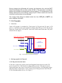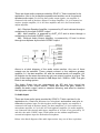
1
TaiChi
Service Manual
1. Preface/Foreword/General Safety Information
Scope of Manual
This manual is intended for use by experienced technicians familiar with similar types of
equipment. It is intended primarily to support basic servicing, which consists primarily of
mechanical repairs and circuit board replacement.
Authorized distributors may opt to receive additional training to become authorized to
perform limited component repairs. Contact your regional Customer Support Manager for
details.
Model and Kit Identification
Motorola products are all specifically identified by an overall model number on the
product FCC label. In most cases, assemblies and kits which make up the equipment also
have kit numbers stamped on them.
Service
Motorola’s regional Cellular Subscriber Service Centers offer some of the finest repair
capabilities available to Motorla Subscriber equipment users. The Cellular Subscriber
Service Centers are able to perform computerized adjustments and repair most defective
transceivers and boards. Contact your regional Customer Service Manager for more
information about Motorola’s repair capabilities and policy for in-warranty and out-ofwarranty repairs in your region.
Replacement Parts Ordering
Motorola maintains a parts office staffed to process parts orders,identify part
numbers,and otherwise assist in the maintenance and repair of Motorola Cellular
products.Orders for all parts should be send to the Motorola (China) Inc.Personal
Communication Enterprise Department Full Quality Service Center Spare Parts
Department at the following address:
Address:
A39,Zizhuyuan Road,Haidian,Beijing
Motorola (China) Inc.
Personal Communication Enterprise Department
Full Quality Service Center Spare Parts Department
Call: 68437222-1011 or 68438724
Fax: 68420990
When ordering replacement parts or equipment information, the complete identification
number should be included. This applies to all components,kits,and chassis.If the
component part number is not known,the order should include the number of the chassis
or kit of which it is a part, and sufficient description of the desired component to identify
it.
General Safety Information
CAUTION
Do not jump start vehicle or use an automotive battery charger while the vehicle adapter
option and the portable radiotelephone are connected to the vehicle electrical system as
this may cause serious damage to the radio. Disconnect the radio by removing the cable
kit tuses.
Portable Operation
DO NOT hold the radio so that the antenna is very close to, or touching, exposed parts
of the body, especially the face or eyes, while transmitting. The radio will perform best if
it is held in the same manner as you would hold a telephone handset, with the antenna
angled up and over your shoulder. Speak directly into the mouthpiece.
DO NOT operate the telephone in an airplane.
DO NOT allow children to play with any radio equipment containing a transmitter.
Mobile Operation
As with other mobile radio transmitting equipment, users are advised that for satisfactory
operation of the equipment and for the safety of personnel, it is recommended that no
part of the human body shall be allowed to come within 20 centimeters of the antenna
during operation of the equipment.
DO NOT operate this equipment near electrical blasting caps or in an explosive
atmosphere. Mobile telephones are under certain conditions capable of interfering with
blasting operations. When in the vicinity of construction work, look for and observe signs
cautioning against mobile radio transmission. If transmission is prohibited, the cellular
telephone must be turned off to prevent any transmission. In standby mode, the mobile
telephone will automatically transmit to acknowledge a call if it is not turned off.
All equipment must be properly grounded according to installation instructions for safe
operation.
All equipment only can be maintained by qualified specialist.
Driving and Mobile Operation
Give full attention to the safety while driving. The driver can only use the mobile
telephone when it is safety. Using wireless telephone while driving in some regions is
illegal .
See relating section of the Products Service Manual for other information of safety.
2.Content
1
2
3
Preface/Foreword/General Safety Information
Content
General Description
3. 1 Product Description
3. 2 Features/Feature List
3. 3 Key Unique Features of the phone
4
5
Taichi Specifications
Identity & Security
5. 1 Transceiver Labelling
5. 2 SIM Card
6 Theory of Operation
6. 1 GSM System Overviw
6. 2 General Cellular Concept
6. 3 GSM Description
7 Detailed Description of Schematic Diagram
7. 1 Transmitter
7. 2 Logic Circuitry
7. 2. 1 GSM Logic Control
7. 2. 2 PDA circuitry
7. 3 Power Supply
7. 4 Charge circuitry
7. 5 LCD circuitry
7. 6 Other circuitries
8 Personality Transfer
8. 1 Introduction
8. 2 Normal Transfer
8. 3 Master Transfer
8. 4 Master SIM Card Creation
9 Test
10 Assembly & Disassembly
10. 1 Introduction
10. 2 Tools Recommended
10. 3 Disassembly
10. 4 Assembly
11 Troubleshooting
12 Accessory
Appendix Replacement parts Ordering and the products saled in
Appendix Equipment &Tools List
Appendix Transceiver Block Diagram
Appendix GSM Logic Diagram
Appendix PDA Logic Diagram
Appendix Detailed Schematic Diagrams
3.General Description
3.1Product Description
Overview
A6188 is a microprocessor controlled, full duplex, synthesized FM radiotelephone using
digital modulation techniques, for use in compatible 900MHz/1800MHz cellular
radiotelephone systems. When operated properly, the equipment will provide the
user with land-linked telephone service through individual cell site base stations,
all linked to a central control office.
Physical Packing
It
introduces
Five
major
new
IC ’s
known
as
WHITECAP,MAGTC,GCAP? ,MCIC, TX-VCO IC and Dragonball.All IC ’s are
BGA parts(Ball Grid Array) except TX-VCO module.The antennas style is
Telescopic direct connect.Vibrator is at the bottom of the back housing and not in
the flip.There is no auxiliary battery. The type of the battery is CD928, and the
charge/discharge parameters are readjusted. The battery selecting circuit is
eliminated.
There are six cans covering the PC board, it uses a mini SIM Card holder and
connector is protected by the battery as in d560 and Modulus? .
The RF power levels of A6188 are the same as for all previous GSM products.
The accessory connector, situated at the top of the A6188 on the main board,
allows connections to the circuity and antenna for accessory applications such as
a mobile adaptor. When the accessory RF connector is used, the RF to the
antenna is disconnected. Grounding shields,(with removable covers) on the main
board provide electrical isolation and protection to the RF circuits.
3. 2 Features/Feature List
Features
Dual Band Capability: The phone can automatically change the phone operation from
GSM band to DCS 1800 band and vice verse.This provides advantages for two
different types of Network Operators:
*A DCS1800 Operator may allow users to roam onto GSM nerworks.
Thus,the DCS1800 user potentially has the same geographical coverage as
a GSM user, often wider than he would with a pure DCS1800 phone.
*A Network Opeator with both GSM and DCS1800 systems may allow users
to use either system.Thus, if the DCS1800 system is busy or there is no
system coverage, the phone can attempt a call on the GSM band and vice
verse.
Taichi Feature List:
Note: The products research work is not completed,so the feature listed below is
subject to changed.
·Selective housing color: gray/silver, size: about 157cc,weight:about
175g(Standard 900mAh Li Battery)
·Li Battery ,900mA, standby time: 130-260 hours,talk time: 4-6 hours.*
·GSM900/1800MHz automatic dual band*
·Icon user interface,full touch display(320*240 Grid Array),including keys such as:
On/Off,Scroll,Volume,Record etc.
·Handwritting identification: Chinese/English. Creating Telephone Book in Chinese
·Sending and receiving short message in Chinese *
·Infrared interface, working with PC(installed Truesync software Chinese version
),can provide functions such as Telephone Book transfering, short message
editing and tranmitting, network access etc.
·Build-in headset jack
·Length of recoding time :3 minutes
·Vibrate alert
·New ringing tones
·Electroluminescent backlight as in Baodian,providing more uniform and efficient
lighting than LED.
·Full rate/Enhanced full rate/Half rate coding, proving high clear voice quality. *
·Supporting Chinese SIM card increment service *
·English/Chinese, Chinese/English dictionary
·Calendar,Schedule,Alarm
·Notepad
·Calculator
·Real time worldwide clock
·Enhanced telephone book, supporting up to 1000 entries
·Supporting telephone book copy between SIM card and mobile telephone
·Sending and receiving email *
·Customing fixed phrase and automatic signature used in short message/email
by user
·Unique base charger and special cable, when working together,can also be
used as the communication connector of the mobile telephone and the PC **
·Carry case, Headset,and toughing pen(free)
* Need system support
3. 3 Key Unique Featuresof the phone
A6188 Key/Unique Features
A6188 operates in GSM 900 and DCS 1800 bands and utilizes phased signaling.It allows
automatic seamless hand over between bands( GSM 900 or DCS 1800) during a
call.This phone supports automatic selection of single band networks in either band
depending on the list of preferred networks. There is no indication to the user which band
the phone is currently operating on other than display of the PLMN.Manual selection of
band mode by the user is not possible although a user may manually select a single
PLMN. Although the A6188 has dual band capability each model is flexed as either a
GSM or DCS primary phone.
4. Taichi Specifications
General
Function
Frequency Range
GSM Specification
890-915 MHz Tx, 935-960 MHz Rx
Channel Spacing
Channels
200 KHz
124 carriers with 8 channels per carrier
DCS Specifications
1710-1785MHz TX
1805-1880 MHz RX
375 carriers with
cahnnels per carrier
8
Modulation
GMSK at BT = 0.3
Transmitter
Phase 5 Degrees RMS, 20 Degrees peak
Accuracy
Duplex Spacing
45 MHz
95 MHz
Frequency Stability
+/- .10 ppm of the downlink frequency
( Rx )
Operating Voltage
+3.9 Vdc to + 6.0 dc ( battery )
Transmit Current
200 mA average, 1.0 A peak
Stand-by Current
Average 10mA ( DR X 2 )
Average 6mA DC X 2, 4
mA DC X 9
Dimensions
140mm(L) X 50mm(W) X 27mm (D)
???
Size (Volume)
157cc ???
Weight
Approximately
160g.
Includes
700mAh Nicad battery pack and
antenna. ???
Temperature Range
-20 °C to +55 °C
-25 °C to +55 °C
Transmitter
RF Power Output
Output Impedance
Spurious Emissions
Power Steps
32 dBm +/- 2dBm
30 dBm +/- 2dBm
50 ohms (nominal)
-36 dBm up to 1GHz, ( <-30dBm >
1GHz ) 22
15
10
Receiver
RF Level
-102 dBm
RX bit error rate ( 100 < 2%
kbits )
Channel Hop Time
500 microseconds
Time to Camp
Approximately 10 seconds
Speech Coding
-100 dBm
< 2%
Speech Coding Type
Bit Rate
Frame Duration
Block Length
Classes
Bit Rate
Encoding
with
Regular Pulse Excitation / Lineara
Predictive Coding with Long Term
Prediction. (RPE LPC with LTP.
13.0 kbps
20 ms
260 bits
Class 1 bits = 182 bits. Class 2 bits = 78
bits
FEC 22.8 kbps
5. Idetity and Security
5.1 Transceiver Labelling
Introduction
Each Motorola GSM transceiver will be labeled with various number configurations.The
following information shows and explains the common labeling titles.
Title Explanations
MSN
The Mechaniacal Serial Number(MSN) is an individual number, uniquely identifying the
unit. The MSN will remain the same throughout the units life, even if the main board is
replaced. Because the MSN is unique to the unit, it is often used for logging and tracking
purposes by Motorola National Service Centres on EPPRS. The MSN is divided into the
sections shown below.
Figure 3: MSN Configuration
MSN 10 digits
3digits
1digit
2digits
4digits
MC
OC
DC
SNR
Model
Code
Origin
Code
Date
Code
Serial
Code
CEPT GSM
This is the International Mobile Station Equipment Identity (IMEI) number. The IMEI is
held in the logic circuity.
If the main board is replaced then the units IMEI will change, therefore the units
labellings should be updated with the new IMEI. An IMEI uniquely identifies a mobile
station equipment to the system, and is divided into the sections shown below.
Figure4 : IMEI Configuration
IMEI 15 digits
6 digits
2 digits
6 digits
1 digit
TAC
FAC
SNR
SP
Type
Approval
Code
Final
Serial
Assembly Number
Code
Spare
REV S/H
This configuration consists of two blocks of two digits, and denotes the software and
hardware versions within the unit. The first two digits correspond to the software version,
and the last two digits correspond to the hardware version. If a version update is carried
out on the unit, the correspongding change information should be made apparent on the
labeling.
Model
The model number defines the type of product. Each product type is issued a common
model number.
Package
The package number is used to determine the type of equipment, the mode in which it
was sold, and the language with which it was shipped.
5.2 SIM CARDS
Introduction
Motorola V998 is designed to work with the mini size Subscriber Identity Module
(SIM). The mini SIM card is inserted between the back housing of the phone and the
battery. The SIM card contains all the personal data required to access GSM services.
Data held by the SIM card includes:
·International Mobile Subscriber Identity
·Temporary Mobile subscriber Identity
·Home system
·Services subscribed to
·PIN and unblocking codes
·Call barring codes
The SIM card may also be capable of storing phone numbers and names.
SIM Card Insertion/Removal
The SIM card must be inserted into the unit correctly so that the card can be read, and the
data checked for validity, before operation on the system will be enabled. The card
contains all of the user’s personal identification numbers and details of the system the
phone operates on.
To remove the mini SIM card from the phone, open the battery door , then remove the
SIM card after removing the battery. Whole information on mini SIM card
insertion/removal can be derived from the unit’s User Gude.
Security Information
To stop unauthorized personnel using your SIM card, the option of using a Personal
Identity Number (PIN) is available. When enabled the option requires (on power up) a
verification number to be entered via the unit’s keypads, before the card can be used.
Three attempts to enter the correct PIN may be made. If after the three entries the correct
PIN has not been entered, the card becomes blocked. To unblock the card an
unblocking/supper PIN code must be entered. Ten attempts to enter the correct
unblocking code are permitted, if after ten attempts the correct code has not been entered,
the SIM card is corrupted and becomes useless.
Another option available for the SIM card is call barring. If subscribed to, the call barring
of incoming and/or outgoing calls may be accomplished by entering a special key
sequence. The key sequence includes a “barring code”, which determines the type of
restriction incorporated, and a password to validate the request. The initial password is
provided when
you subscribe to the service. The password can be changed by entering a set key
sequence.
A valid standard mini SIM card can be used in any working GSM transceiver, regardless
of the manufacturer, which is compatible with the standard mini size SIM card.
To protect the actual unit from unauthorized use, a lock function on the hardware is
available. When enabled, this function requires that a three or four digit unlock code be
entered, via the units keypad, before normal operation of the transceiver can take place.
The lock code can be changed by entering a set key sequence.
Further information on set sequences can be derived from the unit’s User Gude.
6. Theory Of Operation
6.1GSM System Overview
Note
The following description is intended only as a
preliminary general introduction to the Global
System for Mobile communications (GSM)
cellular network. This description is greatly
simplified and does not illustrate the full
operating
capabilities,
techniques,
or
technology incorporated in the system.
6.2General Cellular Concept
The cellular systems are used to provide radiotelephone service in the frequency range
890-960MHz. A cellular system provides higher call handling capacity and system
availability than would be possible with conventional radiotelephone systems (those
which require total system area coverage on every operaing channel) by dividing the
system coverage area into several adjoining sub-areas or cells.
Each cell contains a base station (cell site) which provides transmitting and receiving
facilities, for an allocated set of duplex frequency pairs (channels). Since each cell is a
relatively small area, both the cell site and the radiotelephone that it supports can operate
at lower power level than would be used in conventional system.
Using this technique, radiation on a given channel is virtually contained in the cell
operating on that channel and, to some extent, those cells directly adjacent to that cell.
Since the coverage area of a cell on a given channel is limited to a small area (relative to
the total system coverage area), a channel may be reused in another cell outside the
coverage area of the first. By this means, several subscribers may operate within the same
geographic area, without interference with each other, on a single channel.
6.3GSM Description
Unlike previous cellular systems, GSM uses digital radio techniques. The GSM system
has the following advantages over previous analogue systems:
•
International Roaming – Due to international harmonization and standardization,
it will be possible to make and receive calls in any country which supports a
GSM system.
•
•
•
•
Digital Air Interface – The GSM phone will provide an entirely digital link
between the telephone and the base station, which is, in turn, digitally linked
into the switching subsystems and on into the PSTN.
ISDN compatibility – ISDN is a digital communications standard that many
countries are committed to implementing.. It is designed to carry digital voice
and data over existing copper telephone cables. The GSM phone will be able to
offer similar features to the ISDN telephone.
Security and Confidentiality – Telephone calls on analogue systems can very
easily be overheard by the use of a suitable radio receiver. GSM offers vastly
improved confidentiality because of the way in which data is digitally encrypted
and transmitted.
Better Call Quality – Co-channel interference, handover breakes, and fading will
be dealt with more effectively in the digital system. The call quality is also
enhanced by error correction, which reconstructs lost information.
• Efficiency – The GSM system will be able to use spectral resources in a
much more efficient way than previous analogue systems.
In the figure below, the area bounded by bold lines represents the total coverage area of a
hypothetical system. This area is divided into several cells, each containing a cell site
(base station) operating on a given set of channels which interfaces radiotelephone
subscribers to the telephone switching system.
The radiotelephones themselves are capable of operation on any channel in the
system, allowing them to operate in any cell. Due to the low power requirements for
communications between radiotelephones in a particular cell and the cell site,
operating channels may be repeated in cells which are outside the coverage area of
each other.
For example, presume that cell A operates on channels arbitrarily numbered 1 through
8, cell B opeates on channels 9 through 16, cell C operates on channels 17 through 24
and cell D operates on channels 1 through 8 (repeating the usage of those channels
used by cell A). In this system,subscribers in cell A and subscribers in cell D could
simultanuously operate on channles 1 through 8.
The implementation of frequency re-use increases the call handling capability of the
system, without increasing the number of available channels. When re-using identical
frequencies in a small area, co-channel interference can be a problem. The GSM
system can tolerate higher levels of co-channel interference than analogue systems, by
incorporating digital modulation, forward error correction and equalization. This
means that cells using identical frequencies can be physically closer, than similar cells
in analogue systems. Therefore the advantage of frequency re-use can be further
enhanced in a GSM system, allowing greater traffic handling in high use areas.
By incorporating Time Division Multiple Access (TDMA) several calls can share the
same carrier. The carrier is divided into a continuous stream of TDMA frames, each
frame is split into eight time slots. When a connection is required the system allocates
the subscriber a dedicated time slot within each TDMA frame. User data (speech/data)
for transmission is digitized and sectioned into blocks. The user data blocks are sent
as information bursts in the allocated time slot of each TDMA frame, see Figure 2:
“TDMA Transmission” following:
The data blocks are modulated onto the carrier using Gaussian Mininum Shift Keying
(GMSK), a very efficient method of phase modulation.
Each time an information burst is transmitted, it may be transmitted on a different
frequency. This process is known as frequency hopping. Frequency hopping reduces
the effects of fading, and enhances the security and confidentiality of the link. A GSM
radio telephone is only required to transmit for one burst in each frame, and not
continually, thus enabling the unit to be more power efficient.
Each radio telephone must be able to more from one cell to another, with minimal
inconvenience to the user. The mobile itself carries out signal strength measurements
on adjacent cells, and the quality of the traffic channel is measured by both the mobile
and the base station. The handover criteria and thus be much more accurately
determined, and the handover made before the channel quality deteriorates to the
point that the subscriber notices.
When a radio telephone is well within a cell, the signal strength measured will be
high. As the radio telephone moves towards the edge of the cell, the signal strength
and quality measurement decreases.
Signal information provides an indication of the subscriber’s distance from the base
station. As the radiotelephone moves from cell to cell, its control is handed from one
base station to another in the next cell.
This change is handled by the radiotelephone and base stations, and is completely
transparent to the user.
Service Area
The area within which calls can be placed and received is defined by the system
operators. (Because this is a radio system, there is no exact boundary that can be
drawn on a map.) If the telephone is outside a coverage area, the ∅ (no service)
indicator will illuminate and calls will be unable to be placed or received. If this
happens during a conversation, the call will be lost. There may also be small areas
within a particular service area where communications may be lost.
The radio telephone’s identity information is held by its lcal GSM system in its Home
Location Register (HLR) and Visitor Location Register (VLR). The VLR contains
identity informatino on all local active radio telephones. Should you roam to another
area, system or country the radiotelephones identity information is sent to the VLR in
the new system. The new system will then check the radio telephones details with
your home system for authenticity. If everything is in order it will be possible to
initiate and receive calls whilst in the new area.
7.Detailed description of Schematic Diagram
7.1 Transceiver
The main chip for Taichi RF is MAGIC. The MAGIC IC is intended to support
the needs of the GSM/DCS1800 portable telephone products.
For Taichi the MAGIC IC will provide the first LO (RX VCO) to the receiver at
1325.2 to 1359.8 MHz for EGSM with 400 MHz high side injection, and
1405.2 to 1479.8 MHz for DCS 1800 with 400 MHz low side injection. An
external RF mixer will convert the received signal to 400 MHz. The 400 MHz
signal will then pass through an external SAW filter. The filtered signal will
then enter the IC where it will be mixed with an internally generated 400 MHz
signal to generate baseband I and Q signals. These baseband signals will
then be filtered and amplified to provide RxI and Q. The RxI and Q signals will
be converted into digital outputs and sent over a serial bus. The chip will
provide for AGC control through the SPI bus. TX Data will be input serially.
The present data bit and the three previous data bits will be used to set up
one of 16 possible waveforms based on the sum of Gaussian pulses stored in
a look up ROM. The resulting signal will then be clocked out at a 16X
oversample rate. This data pattern will be input to a four accumulator
fractional N synthesizer with 24 bit resolution. The synthesizer output will be
880.2 to 914.8 MHz for EGSM and 1710.2 to 1784.8 MHz for DCS 1800 with
GMSK modulation and will be directly amplified to the transmitter output. The
reference oscillator will be a free running 26 MHz crystal for MAGIC . AFC will
be provided through the SPI bus as a programming offset to the fractional N
division system. Resolution will be approximately 3Hz (6 Hz with Pass 2) with
relative accuracy of less than 1Hz (2 Hz for Pass 2). Since the 26 MHz crystal
will not be locked to the AFC, a second fractional divider system will be
provided to derive an accurate 200kHz reference. This reference will then be
multiplied in a PLL to 13MHz for use as an accurate clock to the logic sections
of the radio.
Two tracking regulators will be provided to power the IC. A superfilter will also
be provided to power the external main VCO.
Finally, an interface system of digital to analog converters will be provided to
control the PAC IC. This will allow the logic sections of the radio to transmit
data over SPI and then activate the transmitter with a single digital line as
opposed to the present D/A output and saturation correction software.
Reference Oscillator
The reference oscillator will use a crystal at 26 MHz for MAGIC with a stability
over temperature of ± 20 ppm for GSM and ±11ppm for DCS 1800 to cover
the camping requiremments in Taichi. An SPI controlled AFC is provided for
by offsetting the fractional N division. Since an accurate clock is needed for
the logic sections of the radio, a secondary fractional N division system is
provided to derive an accurate low frequency clock. This low frequency clock
is then multiplied up in the reference oscillator step up loop to an output
frequency of 13MHz. The reference oscillator will be within 150ppm of 26MHz
within 100msec of the REG_REF input rising to 2.775V.
The 13MHz reference will be provided externally for the logic sections as a
CMOS output at 1Vp-p at CLK_OUT. At power up, the crystal oscillator
divided by 2 will be routed to the CLK_OUT pin by pulling CLK_SEL low. An
SPI bit is then used to activate the digital AFC. Finally CLK_OUT is pulled
high to route the output of the multiplied 200kHz reference to the CLK_OUT
pin.
RX 2nd Local Oscillator
The 2nd LO VCO will be 800 MHz for both GSM and DCS-1800 in the Taichi
radio with the MAGIC IC. The VCO frequency will be divided by 2 internal to the
IC. Note that in the programming the factor of two is ignored so that if an IF
frequency of 400MHz is desired, the programming is calculated as if the LO
was at 400MHz even though it is actually at 800MHz.
Power Supplies
The IC will contain 2 tracking regulators (external PNP or PMOS pass
transistors) which will generate the supplies for the entire IC as well as the
front end and the main VCO. A voltage of 2.775v must be provided to the
REG_REF input. This pin has a maximum current draw of 200µA in mode.
The reference voltage will be filtered and buffered for use on the IC. The
buffered voltage should track the reference within ± 50mV. A raw supply
voltage will be provided to the IC tracking regulators which will be at least
100mV above the reference (50mA output) and could be as high as 6.5Vdc. A
superfilter will be needed for the external VCO power supply. This superfilter,
cascaded with the normal regulator and any filtering in front of the IC, will
need to provide 80dB of rejection to a 0.1V step (risetime = 20µS) in the raw
supply (battery). The superfilter will use an internal pass transistor that will be
capable of driving a 45mA load with a voltage drop of less than 300mV
relative to V2_OUT from the SF_OUT pin. An external .01µF cap will be
required on SF_OUT.
All supplies within the IC must be within 5% of their final values after 10msec.
The power on reset circuit contained within the crystal reference oscillator
may be used to aid this functionality.
Magic / Whitecap MQSPI Interace
The following is the interconnection between MAGIC and WHITECAP in Taichi:
Board
Name
Signal
DX1
MQSPI CLK1
Pin WHITECAP
ball
J3,
Ball
M7,
SPI DATA
output
H4, SPI
CLK_SC Ball
M8,
MAGIC ball
Ball
input
Ball
MAGIC
Name
WHITECAP
Signal Name
DX1
MQSPI CLK1
MQSPI CS1
input
Ball
input
CLK4
G5,
CE
DR1
output
Ball
output
Ball
output
L8,
P5,
MQSPI CS1
DR1
DX1 (SPI_DATA): Serial Peripheral Interface Data, Data will be transmitted
from WhiteCap to the
MAGIC IC. Data will be latched into MAGIC either on rising edge or falling
edge of clock depending on the control bit settings.
MQSPI_CLK : Clock used to shift data out serially.
MQSPI_CSI : Chip select signal used to latch data into MAGIC.
DR1 : Not connected to MAGIC .
MAGIC will interface with the Serial Peripheral Interace 1 (SPI1) of the WHITECAP
IC. Data on the bus will be changed on the fallling edge of the clock and sampled on
the rising edge. The IC will only accept data if a valid chip select is given (active
high) and data is latched in on the falling edge of MQSPI_CS1. There are 4
groups of SPI bits. Data is written most significant bit first. Each SPI transfer
must consist of the full 64 bit field. Thus, additional dummy bits must be
padded to those sequences which are not full length. The two most significant
bits are used to select which SPI group is addressed.
7.2 Logic circuitry
7.2.1 GSM Logic
We call the GSM signal processing control circuit as GSM logic. GSM logic
employed two main chip for its operations – WhiteCap and GCAP-II.
There are two function parts in WhiteCap which provides digital signal processing
and general control.
The WhiteCap IC is a digital processing IC for GSM radiotelephones. It
contains a TI cLEAD DSP core, a TI ARM/Thumb microcontroller core and
custom peripherials implemented in TI’s TSC5000 ASIC standard cell
technology. This part will be used for s/w and radio development.
The DSP core contains 80K words of DSP RAM for software development.
The production version of this part will store DSP and ARM boot-code in onchip ROM.
Whitecap contains the following:
•
ARM7TDMIE core (Thumb 32/16 bit micro controller core)
•
cLEAD Mega Module (DSP w/ 80K words RAM + ARM-API + BBIF-API
+ SP + DPLL)
•
ASIC Microcontroller peripherals
• Memory Interface
• Deep Sleep Controller
• Layer1 Timer
• MQSPI
• SIM Card Interface
• Two UARTs with Infrared Rx/Tx data capability and
• DMA for multi-slot high-speed GSM data service
• One Wire Interface
• Watchdog Timer
• Clock Monitor
• ARM Interrupt Handler (AINT)
• DSC Interface
• GPIO
• Deep Sleep Controller (DSM)
•
ASIC DSP peripherals
• DSC Interface
• Encryption Co-Processor
• GPIO
• Lead Interrupt Handler (LINT)
• Baseband Interface
•
Special Cells
• Clock Monitor
• Input Clock Amplifier
• Battery Power Switch
WhiteCap chip’s block diagram shows as below:
WhiteCap Block Diagram
GCAP-II integrated nearly all the analog functions into one chip, those funcitons
includes power supplies, voltage regulators, A/D and D/A converters for battery
charger, audio CODEC, real time clock, and amplifiers for speaker and microphone
etc. This chip is intended to support the needs of portable cellular telephone products.
It provides control, audio, and regulator functions of the Taichi radio. The following
functions are performed:
-
Turn On control signals to properly activate the radio
Turn off control signals to turn off the radio if an error is detected
Audio amplification for the speaker
Audio amplification for the alert
Audio amplification for EXT audio
Audio amplification fo the microphone
13 bits linear audio CODEC
Band gap reference voltage
Linear regulators for DC voltages
Two BUCK/BOOST switching regulators
Op-amps for use in the battery charger
Internal D/A for the battery charger
-
8 Channel 8 bit A/D
PA high end regulator
Real Time Clock ( RTC )
The detail applications for this chip in Taichi can be found in GSM block
diagram.
7.2.2 PDA Control Logic
PDA logic mainly provides the interface control functions for Taichi radio.
DragonBall is the core chip which fetchs executive code from external flash
memory through data bus and address bus.
DragonBall introduced by Motorola as the newest member of the DragonBall’s
Series of MC68328 family.
Inherited the display capability of the original DragonBall’s processor, the
MC68EZ328 features a more flexible LCD controller with streamlined list of
peripherals placed in a smaller package. This processor mainly targeted for
portable consumer products which require less peripherals and a more flexible
LCD controller. By providing 3V, fully static operation in an efficient 100 TQFP
package, the MC68EZ328 delivers cost-effective performance to satisfy the
extensive requirements of today's portable consumer market.
DragonBall has the following features:
•
Static
68EC000
Core
Processor-Identical
to
MC68EC000
Microprocessor
1. Full Compatibility with MC68000 and MC68EC000
2. 32-Bit internal address bus
3. 24-Bit external address bus capable of addressing maximum 4 x 16MB
blocks with chip selects CSA, CSB and 4 x 4 MB blocks with chip
selects CSC, CSD.
4. 16-Bit on-chip data bus for MC68000 bus operations
5. Static design allows processor clock to be stopped to provide power
savings
6. 2.7 MIPS Performance at 16.58 MHz processor clock
7. External M68000 Bus interface with selectable bus sizing for 8-bit and
16-bit data ports
•
System Integration Module (SIM28-EZ), Incorporating Many
Functions Typically Related to External Array Logic, such as:
1. System configuration, programmable address mapping
2. Glueless interface to SRAM, EPROM, FLASH memory
3. 8 programmable chip selects with wait state generation logic
4. 4 programmable interrupt I/O and with keyboard interrupt capability
5. 5 general purpose, programmable edge/level/polarity interrupt IRQ
6. Other programmable I/O, multiplexed with peripheral functions up to 47
parallel I/O
7. Programmable interrupt vector response for on-chip peripheral
modules
8. Low-Power mode control
•
DRAM Controller
1. Support CAS-before-RAS refresh cycles and self-refresh mode DRAM
2. Support 8 bit / 16 bit port DRAM
3. EDO or Automatic Fast Page Mode for LCDC access
4. Programmable refresh rate
5. Support up to 2 banks of DRAM/EDO DRAM
6. Programmable column address size
•
UART
1. Support IrDA physical layer protocol up to 115.2kbps
2. 8 Bytes FIFO on Tx and 12 Bytes FIFO on Rx
•
Serial Peripheral Interface Port
1. 16 bit programmable SPI to support external peripherals
2. Master mode support
•
16-Bit General Purpose Counter / Timer
1. Automatic interrupt generation
2. 60-ns resolution at 16.58-MHz system clock
3. Timer Input/Output pin
•
Real Time Clock / Sampling Timer
1. Separate power supply for the RTC
2. One programmable alarm
3. Capable to count up to 512 days
4. Sampling Timer with selectable frequency (4Hz, 8Hz, 16Hz, 32Hz,
64Hz, 256Hz, 512Hz, 1kHz). Generate interrupt for digitizer sampling,
or keyboard debouncing.
•
LCD Controller
1. Software programmable screen size ( up to 640*512 ) to support single
(Non-Split) monochrome/ color STN panels
2. Capable of direct driving popular LCD drivers/modules from Motorola,
Sharp, Hitachi, Toshiba etc.
3. Support up to 4 grey levels out of 16 palettes.
4. Utilize system memory as display memory
5. LCD contrast control using 8-bit PWM
•
Pulse Width Modulation (PWM) Module
1. 8 bit resolution
2. 5 Byte FIFO provide more flexibility on performance
3. Sound and melody generation
•
Build-in Emulation Function
1. Dedicated memory space for Emulator Debug Monitor with Chip Select
2. Dedicated interrupt (Interrupt Level 7) for ICE
3. One address signal comparator and one control signal comparator with
masking to support single or multiple Hardware Execution Breakpoint
4. One breakpoint instruction insertion unit
•
Boot Strap Mode Function
1. Allow User to initialize system and download program/data to system
memory through UART
2. Accept execution command to run program stored in system memory
3. Provide an 8-byte long Instruction Buffer for 68000 instruction storage
and execution
•
Power Management
1. Fully static HCMOS technology
2. Programmable clock synthesizer using 32.768 kHz/38.4 kHz crystal for
full frequency control
3. Low power stop capabilities
4. Modules can be individually shut-down
5. Lowest power mode control
•
•
•
Operation from DC To 16.58 MHz (processor clock)
Operating Voltage of 2.7V-3.3V
Compact 100-Lead Thin Quad Flat Pack (TQFP) and 144 Pin Ball Grid
Array (PBGA) packages
This chip’s block diagram is showing as below:
DragonBall Block Diagram
LCD module gives the user an visible interface. Detailed LCD module descriptions
can be found in LCD module circuit description. The connections between
DragonBall and LCD module are joint by J9805. There is one EL panel on LCD
module which can give backlight in darkness environment. U9812 drives IR diodes
for communication link between PC and DragonBall. Alert circuit is also controlled
by DragonBall. Alert circuit is also controlled by DragonBall. Analog switches
provide multiple communication path control which give the serial port different link
under different use conditions. Refer to the PDA logic block diagram.
7. 3 Power Supplies
Global Control Audio Power II ( GCAP-II ) is a power and audio management IC. It
incorporates many of the functions of various different power and audio management
Ics into one platform. For power supplies, GCAP-II provides five programmable
linear regulators ( VSIM1, Ref, V1, V2, and V3 ) which give all voltages for the logic
IC’s and two Buck or Boost switching regulators ( PWM #1 and PWM #2 ).
Power Management
•
PGM0,1,2 Hardware configuration
PGM0 and PGM1 alone determine the battery mode of GCAP-II. This is necessary
because the startup and shutdown voltages need to be available without processor
intervention. At power-up PGM2 alone determines the output of V3. If PGM2 is
connected to B+, V3 is 2.775V. If PGM2 is connected to ground, as in Taichi, V3 is
2.003V. No processor intervention is necessary.
•
V2 Linear Regulator
V2 is a programmable linear regulator. It is programmed through the SPI bus to
outputs from 2.775V to 3.6V in 0.12V steps. For Taichi V2 is programmed to 2.775V.
The regulator is supplied by B+. This regulator is on whenevey the radio is turned on.
V2 is the supply for WhiteCap logic outputs, RAM FLASH, and display.
•
V3 Linear Regulator
V3 is a programmable linear regulator with an output voltage which is determined by
PGM2 at power-up. It is either 2.008V if PGM2 is connected to ground or 2.775V if
PGM2 is connected to B+. After power-up V3 can be programmed through the SPI
bus to voltages from 1.8V to 2.8V in 0.13V steps.For Taichi V3 is programmed to
1.8V.The regulator is supplied by B+. V3 is the fupply for the WhiteCap core (does
not include logic output supply). For example, V3 supplies the ARM core, Clock
amplifier, DSP Core, and input logic. For RAM 2 Whitecap V3 is programmed to
1.8V.
•
VSIM Regulator
VSIM is a programmable linear regulator. It is programmed through the SPI bus to
either 5.0V or 3.0V. For TaiChi VSM is programmed dynamically to 5.0V. VSIM is
spplied by V_BOOST1 and supplies the SIM card.
•
V1 Regulator
V1 is a programmable linear regulator. It is programmed through the SPI bus to either
5.0V or 2.775V. For Taichi V1 is programmed to 5.0V and is supplied by
V_BOOST1. This regulator is on whenever the radio is turned on. V1 supplies the
DSC bus.
•
V_BOOST1 Switcher Regulator
V_BOOST1 is a switching regulator. At power up pins PMG0 and PMG1 determine
the mode of the switcher. For Taichi V_BOOST1 is programmed to 5.6V because
PMG0 is shorted to B+ and PMG1 is shorted to ground. The regulator is on whenever
the radio is turned on. V_BOOST1 supplies V1 and VSIM.
•
V_BUCK Switcher
V_BUCK is a switching regulator. At power up, pins PMG0 and PMG1 determine the
mode of swither. For Taichi V_BUCK is not used.
•
PA_DRV Alert/Backlight Regulator
PA_DRV is a programmable linear regulator which drives an external P channel
MOSFET. It is programmed by setting PA_B3-0 to one of 16 codes corresponding to
an output of 2.6V to 7.00V incremented by 0.40V steps. Initially PA_DRV is off until
set via SPI. For Taichi PA_DRV regulates ALRT_VCC to 3.0V (PA_B3-0 = 000).
This regulator is turned on and off by LS3_TX if PA_ON1 is enabled (high).
PA_DRV powers the alert and backlights.
7.4 Battery Charge
Taichi battery
There is a charge control circuit built into Taichi radio. When a battery is
attached and with a external charger insert into the radio through BUTTPLUG, the radio will charge the attached battery according to the battery type.
Before describing this radio charger circuitry, lets introduce the battery
package itself.
There is four pins output from battery package: Serial Data, Ground, Power( +
) and Thermister.
SERIAL DATA connection is used by GSM radio to communicate to and
from the internal EEPROM, located inside the battery, to the radio’s
microprocessor. This bi-directional line is used to adjust the operation of the
battery charger and battery meters.
GROUND connection is used as a reference ground for the battery to the
GSM radio.
POWER ( + ) connection provides sufficient voltage to the GSM radio. The
voltage range of a GSM battery ranges from 1.4 volts DC (fully discharged) to
5.1 volts DC (fully charged).
During charging the Whitecap will monitor the thermister line and the BATT
Sense line through A/D convertor within GCAP-II. The thermister is inside the
battery and indicates its temperature during charging. The temperature of the
battery defines the end of battery charge cycle in some cases and must be
monitored continuously during charging.
The energy flows along the dashed wider line from EXT_B+ to BATT+ as
above diagram indicated.
7. 5 LCD module
1. Overview
Taichi LCD module is assembled by Touch panel, LCD panel and EL panel. LCD
panel is a 320X240 pixels with transflective display film,STN type LCD. The driving
signals for Touch panel, LCD and EL come from Taichi main board and LCD power
circuit PCB. See figure 1.
Touch screen control lines
EL control lines
- EL (GND), EL (+)
Data lines
- D0, D1, D2, D3
Control lines
- Disp, Loadse, Loadco, Dfseg, Dfcom,
Frame, CP
Power lines
Column driver IC (320 outputs)
- Right, Top, Left, Bottom
Touch screen
1/4 VGA
resolution LCD
EL panel
VD1, VD2, VM, VS12, Vdd, Vcc, Vss
Row driver IC
(120 outputs)
Row driver IC
(120 outputs)
Fig.1 LCD module electrical block diagram
2. Driving signal for LCD panel
2.1 LCD panel electrical block
LCD panel is driven by signals come from Dragonball microprocessor and LCD
power circuit PCB. LCD controller in Dragonball generates LCD logical control
signal and display data. Power circuit PCB is used to generate LCD operating voltage
and temperature compensation. It also controls power management for the PCB and
LCD common&segment drivers. See Figure 2.
D0,D1,D2,D3
LCD Panel
LCLK, LLP,LLP,LACD
Main
Board
VSS
Disp
Dfram
Frame
LCD
Controller
VD1
VD2
VM
Vdd
Vcc
Vss
LLP,LFRAM
EZ328
DOFF, LACD
VOL1,VOL2,VOL3
LCDPCB
Power management
Timing control
Temp.compensation
VDD,VSS
Figure 2.Taichi LCD Panel Electrical Block
2.2 Driving signal from LCD controller
The function of each signal is as follows:
D0-D3---------LCD data bus is used to transfer pixel data to the LCD panel.
LFRAME-----LCD frame scan signal indicates the start of a new frame.
LLP------------LCD line scan signal is used to latch a line of shifted data.
LCLK---------LCD shift clock signal is the clock output which the display data is
synchronized.
LACD---------LCD alternate crystal direction output signal is toggled to alternate
the
crystal polarization on the panel.
DOFF----------LCD ON/OFF control signal.
Figure 3 is the timing waveform for these signals.
1 FRAME
FRAME
LOAD
LOAD
2
1
3
77
4
78
79
80
SCLK
D0
D1
S1
S5
S9
S305
S309
S313
S317
S2
S6
S10
S306
S310
S314
S318
S3
S7
S11
S307
S311
S315
S319
S4
S8
S12
S308
S312
S316
S320
D2
D3
Figure 3. Waveform for LCD control and data signals
3.Driving signal for EL
A DC/DC converter generates EL driving voltage. See Figure 4.
3.3V
0.68mH
L+
L-
EL+
Vout
D358-D
V+
NC
CLF
2.2uF
GND
E
EL ON/OFF
0.01uF
EL Panel
Figure 4. EL Driving Circuit
The waveform of EL+ shows in Figure 5
EL+(V)
100
t(ms)
2.8
-100
Figure 5. EL+ Driving Signal
4.Touch panel driving signal
A 12-bit A/D converter is used to generate an interrupt request signal to Dragonball
,receive control instruction and sample and transmit touch data from Touch panel to
Dragon. See Figure 6.
Main Board
RIGHT,TOP,LEFT,BOTTOM
A/D
SPI
IRQ5
EZ328
Figure 6. Taichi Touch Panel Block
7.6 Other circuitries
Audio Management
1. Audio Output
Touch Panel
There are three audio outputs provided by GCAP-II, Taichi used two for its
application. One is for its earpiece speaker and another one is for external
speaker audio output. For driving those audio output signals, one amplifier is
connected with each of the three outputs. For those amplifiers: A1 is for transceiver
earpiece speaker amplifier, A2 is for Alert amplifier and A4 is for External audio
output amplifier.
A1 – Earpiece Speaker Amplifier, is powered by V2 and is driven through a
multiplexer by the audio CODEC output.
A2 – Alert amplifier. Is powered by ALRT_VCC and is driven through a
multiplexer by the audio CODEC output.
A4 – External Audio Output Amplifier, is powered by V2 and is driven
through a multiplexer by the audio CODEC output.
Above is a block diagram of the audio output section. Any one of three
outputs can be selected. These outputs connect to the earpiece speaker
amplifier, A1, the alert amplifier, A2, and the external audio out amplifier, A4.
All outputs use the same converter so only one output is active at a time. The
gain of the output can be selected in 5dB steps from -35dB to +0dB. This gain
block is an analog system.
The Audio Output bits are programmed via SPI and they control the
configuration of the output section. These bits select the gain, enable or
disable the audio output, select or deselect dithering, and select or deselect
the high pass output filter.
2. Audio Input
There are three audio inputs provided by GCAP-II, Taichi used two for its
application also. One is for its transceiver microphone and another one is for its
external microphone input. For driving those audio input signals, one amplifier is
connected with each of the three inputs. For those amplifiers: A3 is for transceiver
microphone amplifier, A5 is for the AUX microphone Amplifier. No audio amplifier
was connected with external audio input. Amplifiers of A3 and A5 are powered by V2
and drive the audio CODEC input. Taichi phone use the without amplification
external microphone input for the headset microphone.
Below is the block diagram of the audio input section. Any one of three equivalent
microphone inputs can be selected. These inputs are EXT_MIC, the output of the
differential input microphone amplifier, A3 or , the output of the differential
auxiliarymicorphone amplifier, A5.
These three inputs are single ended with respect to VAG.
Note that MIC IN+ should be DC connected to VAG to avoid an offset relative to the
A/D input. MIC_BIAS is derived from VAG for best noise performance. MB_CAP
bypasses the gain from VAG to MIC_BIAS to keep the noise balanced.
Following the input stage and multiplexer is a selectable gain stage and
30kHz low-pass antialiasing filter. This lowpass filter may be designed to
whatever order is needed to insure that aliased components are not present in
the output. The gain of the selectable gain stage can be selected in 1dB steps
from -7dB to +8dB. Depending on the design of the A/D converter the output
of the antialiasing filter may be clamped to keep from overdriving the A/D
converter.
The audio input A/D converter converts the incoming signal to 13-bit 2's
compliment linear PCM words at an 8 or 8.1 kHz rate. Following the A/D
converter, the signal is digitally filtered, low-pass and selectable high-pass.
The audio input bits control the configuration of the input section. These bits
select the gain, enable or disable the input, select between the EXT_MIC, A5
amplifier output, or A3 amplifier output, and select or deselect the high pass
input filter. Also, these bits can select a loopback mode that takes the digital
output of the input A/D converter, and loops it directly back to the D/A output
section for testing.
WhiteCap Logic Interfaces
1.DSC Module
The DSC module implements the GSM Data Speech Control interface in the
Whitecap IC. It accepts manchester encoded data input on the DSC bus and
generated manchester coded data onto the DSC bus. DSC data may be
transmitted to or received from the TI LEAD megamodule or TI ARM
megamodule via the XIO interface and PIF interface, respectively. The PIF
interface also provides control of the DSC module.
The DSC module generates a clock and frame sync to the audio codec
interface. The frame sync is synchronized so the DSC LEAD interrupt occurs
at the same time as the Audio CODEC interrupt. An ARM interrupt is
generated to synchronize the ARM megamodule to the DSC interrupt. The
DSC time slots are the basic data structures in the DSC module. The function
of the DSC is to transmit and receive DSC frames on the DSC bus. These
frames may come from or be sent to the Lead DSP Audio Coder XIO port, the
ARM Call Processor PIF port, or the Manchester coded DSC bus.
The DSC module in Whitecap operates only in the Master mode at a
controllable bit rate of 128kHz or 512kHz. The audio CODEC clock always
operates at 512Khz. Switching the DSC from 128kHz to 512kHz is held off
until DSC time slot boundaries. This functionality is changed from BIC 4.X for
the Whitecap DSC module to accommodate the CODEC interface and
synchronization for the Lead DSP.
2. UART-RS232
The UART is based upon a TL16C550 compatible UART. It is used to
communicate serially over an RS232 interface. The module sends and
receives characters of 8 bits. The number of stop bits can be programmed to
1 or 2. Parity can be programmed to even, odd, or disabled completely. The
module contains a 32 deep FIFO for the received characters and a 16 deep
FIFO for transmit. It generates its own baud rate based upon a programmable
divisor and its input clock.
3.SIM INTERFACE
The SIM Interface is a peripheral in the Whitecap Chip that allows the ARM
Core to communicate with pre-paid cards or SIM cards. It communicates with
the ARM via the 16-bit internal Peripheral Bus. The SIM interface contains 2
ports, one allowing synchronous or asynchronous ( pre-paid cards ) serial
transmission and the other allowing only asynchronous serial transmission.
8. Personality Transfer
8. 1 Introduction
Due to the different variations of the (OEM looks) of the personal cellular
telephones, each main board must be configured correctly to ensure that the
unit takes on the correct personality required. Therefore, when a main board
is replaced its personality must be transferred into the new board, so that it
functions correctly in the customers unit. There are two possible methods of
transfer:
·Normal Transfer,and:
·Master Transfer.
If the defective unit powers up, then the Normal Transfer method should be
followed. If the faulty unit will not power up, then a Master transfer will be
required to configure the replacement board, once installed.
8. 2Normal Transfer
This method allows the personality, selected features and stored phone
numbers of a defective radio, to be transferred into a repaired radio. Data is
transferred from the donor unit into the recipient unit using a Transfer card
(Part No 5104025D01).The instruction steps should be followed in order.
Step 1: Insert the Transfer card into the slot located on the back of the donor
unit.Turn the donor unit on, the display should show‘Clone’.
Step 2: The donor unit is now in the cloning mode, and ready to transfer the
first block of data.
Step 3: Enter 021# via the units keypad.This command will cause the first
block of information to be uploaded into the Transfer card.
Step 4: While data transfer is taking place between the unit and the card,
‘Please wait’ will be displayed. After a short period of time, if the data transfer
has been completed correctly, ‘Clone’will re-appear in the donor units display.
Step 5: When the first data block has been successfully uploaded, remove
the card from the donor.
Step 6: Insert the Transfer card into the slot located on the back of the
recipient unit. Turn the recipient unit on, the display should show ‘Clone’.
Step 7: The recipient unit is now in the cloning mode, and ready to receive
the first block of data.
Step 8: Enter 03# via the units keypad. This command will cause the
recipient unit to download the first data block from the Transfer card.
Step 9: While data transfer is taking place between the card and the unit,
‘Please wait’ will be displayed. After a short period of time, if the data transfer
has been completed correctly, ‘Clone’will re-appear in the recipient units
display.
Step 10: The second data block must now be transferred. Repeat steps 1 to
9, but enter 022# to program the second data block into the Transfer card.
Step 11: The third data block ( known as table5# ) must now be transferred.
Repeat steps 1 to 9, but enter 025# to program the third data block into the
Transfer card.
Step 12: When the third block of data has been transferred
successfully,remobe the Transfer card and check the repaired radio
functions correctly. See to the information in ‘Testing’.
8. 3 Master Transfer
This method of transfer should only be followed when the defective unit will
not power up, or complete a Normal Transfer. As mentioned earlier, there are
different variations (OEM looks) of the Motorola cellular telephones, each
model requiring the main board to be configured differently for correct
operation. When carrying out a Master Transfer it is not possible to transfer
the customers selected features or stored phone numbers, only the
personality can be programmed into the repaired unit.
Each different version of the cellular telephone, has its own Master card which
contains essential set up information. Master SIM cards may be ordered
preprogrammed, or created from a Normal Transfer card. The instruction
steps should be followed in order.
Step 1: Select the required Master SIM card.
Step 2: Insert the Master Transfer card into the slot located on the back of the
repaired unit.Turn the donor unit on, the display should show‘Clone’.
Step 3: Enter 04# via the units keypad.This command will cause the
configuration data to be downloaded from the Master Transfer card.
Step 4: While data transfer is taking place between the card and the unit,
‘Please wait’ will be displayed. After a short period of time, if the data transfer
has been completed correctly, ‘Clone’will re-appear in the recipient units
display.
Step 5: When the third block of data has been transferred
successfully,remobe the Master Transfer card and check the repaired radio
functions correctly. See to the information in ‘Testing’.
At no point should either 021# or 022# be entered while a Master Transfer
card is in the radio. If either of the stated commands is entered, the master
information on the card will be erased. To prevent the above happening the
card can be locked by entering 06# via the units keypads, with the card
inserted. Unlocked the card by entering 07# .
·If during either transfer process a problem arises, an error message will be
displayed. If the Transfer card is removed before the data transfer is
completed ‘Bad Data on Card’ will appear in the display. If either situation
arises, the process should be repeated.
8. 4 Master SIM Card Creation
When required a Master SIM card can be created by:
Step 1: Insert a Transfer card into a unit which is already configured in the
desired way.Turn the unit on, the display should show‘Clone’.
Step 2: Enter 024# via the units keypad.This command copies the personality
information in the unit onto the Transfer card to create a Master Transfer
card.?
Step 3: While data transfer is taking place between the unit and the card
‘Please wait’ will be displayed. After a short period of time, if the data transfer
has been completed correctly, ‘Clone’will re-appear in the recipient units
display.
Step 4: A Master Transfer card has now been created. Lock the card to
prevent accidental information erasure (the card can be locked by entering
06# via the units keypad, with the card inserted).Remove the card from the
unit, and store until required.
9 TESTING
GSM Verification
Introduction
To test the phone for functional verification,the following equipment is
required.
• GSM compatible communications analyzer.
• Antenna test adaptor (Part Number SKN4870A) and an appropriate
cable/connectors.
• Test SIM card (Part Number8102430Z01).
• Charged battery pack.
Equipment Configuration
Initially insert the test SIM card into the slot at the rear of the personal cellular
telephone. If required, further information on SIM card insertion is available on
page 18. Slide a charged battery on to the back of the phone, so that the
telephone can be powered up. Finally, connect a cable from the accessory
connector to the RF in/out port of the communication analyzer, and power
both the analyzer and personal telephone on. The equipment set up shown in
figure .. “GSM/DCS testing configuration should now be in place.
GSM/DCS Manual Test Mode.
Introduction
Telephones are equipped with a Manual Test Mode capability. This capability
allows service personnel to take control of the tele-phone. and by entering
certain keypad sequences, make the telephone perform desired functions. to
enter the Manual Test Mode, a test SIM card (Part number 8102430Z01) is
required.
DCS Testing Procedure
All information required to perform the desired tests and measurements,
should be obtained from the communication analyzer’s manual. Ensure that
the unit being tested is capable of both initiating a call to the analyzer, and
recieving a call from the analyzer. Confirm thet the displayed Temprary Mobile
Subscriber Identify (TMSI), International Mobile Equipment Identify (IMEA),
and dialled number are correct. When a call is in progress the following tests
should be carried out on channels 512, 700, and 885. The recorded results
must be within the acceptable stated limits, if the unit being tested passes all
the tests it should be taken as functioning correctly. If the unit being tested
fails to confirm with any of the expected measurements, it should be taken as
faulty and repaired accordingly.The following table states the required test and
tolerances.
Accessing The Manual Test Mode
• When the Test SIM card is in place, power up the telephone. Once the initial
automatic ‘wake up’ sequence has taken place correctly, depress the # key
(on the units keypad) for three seconds. After three seconds ‘TEST’ should
appear in the display, indicating that the unit is now in the Manual Test Mode.
The table below shows the avail-able Manual Test commands and their corresponding results.If a customer should forget the security code in their unit, it
can only be read or changed by using a Test SIM card.
General Information For DCS Radios
• Number of Channels are 375.
• Low Channel Number 512.
• Low Channel Tx Freq 1710 MHz.
• Low Channel Rx frequency 1805 Mhz.
• Mid Channel number 700
• Mid Channel Tx Freq 1747.8 MHz.
• Mid Channel Rx Frequency 1842.8 MHz
• High Channel Number 885
• High Channel Tx Frequency 1785 MHz.
• High Channel Rx Frequency 1880 MHz.
GSM/DCS Key Sequence
#(hold down for 2 seconds)
01#
02xxyyy#
03x#
05x#
07x#
08#
09#
10#
11xxx#
12xx#
13x#
14x#
15x#
16#
19#
20#
22#
24x#
GSM/DCS Test Function/Name
Enter manual test mode
Exit manual test mode
Display/modify TX power level DAC &
load PA calibration table
DAI
Initiate Exec Error Handler Test
Mute RX audio path
Unmute RX audio path
Mute TX audio path
Unmute TX audio path
Program main LO to channel
Set TX power level to fixed value
Display memory block usage
Initiate Out of Memory condition
Generate tone
Mute tone generator
Display S/W version number of Call
Processor
Display S/W version number of Modem
Display S/W version number of Speech
Coder
Set step AGC
25xxx#
26xxxx#
31x#
32#
33xxx#
34xxxyy#
36#
37#
38#
39#
40#
41#
42#
43x#
45xxx#
46#
47x#
51#
52#
57#
58#
58xxxxxx#
59#
59xxx#
60#
61#
61xxx#
62#
62xx#
63#
63xxxxx#
64#
64x#
65#
GSM/DCS Key Sequence
66xyyy#
67#
68#
69x#
70xxyyy#
71xx#
72xx#
73xyyy#
7536778#
Set continuous AGC
Set continuous AFC
Initiate Pseudo-Random Sequencewith Midamble
Initiate RACH Burst Sequence
Synchronize to BCH carrier
Configuration to TCH/FS & Enable
TCH loopback w/o Frame Ensure
Indication
Initiate acoustic loopback
Stop test
Activate SIM
Deactivate SIM
Initiate sending all 1’s
Initiate sending all 0’s
Disable echo processing
Change audio path
Serving cell power level
Display current value of AFC DAC
Set audio volume
Enable sidetone
Disable sidetone
Initialize non-volatile memory
Display security code
Modify security code
Display lock code
Modify lock code
Display IMEI
Display MCC portion of the LAI
Modify MCC portion of the LAI
Display MNC portion of the LAI
Modify MNC portion of the LAI
Display LAC portion of the LAI
Modify LAC portion of the LAI
Display Location Update Status
Modify Location Update Status
Display IMSI
GSM/DCS Test Function/Name
Display/modify TMSI
Zero PLMN Selector
Zero forbidden PLMN list
Display/modify Cipher Key Sequence
Number
Display/modify BCCH allocation table
Display internal information
Display Passive Fail codes
Display/modify Logger Control Block
Initiate transfer to Flash Memory
980#
981#
DCS Mode
GSM Mode
Table 1:
DCS Test to be performed
Lower Limit
Upper Limit
Transmit average phase error (RMS) at max and
5 degrees
min power
Transmit average phase error (peak) at max and
20 degrees
min power
Transmit average frequency error at max and
-90Hz
+90Hz
min power
Transmit power error at level 7 (29 dBm)on
-2db
+2db
CH62
Transmit power error at level 10 (23 dBm)on
3db
+3db
CH62
Transmit power error at level 15 (13 dBm)on
-3db
+3db
CH62
within DCS specification
Transmit power error at max and min power
envelope
Receive Bit Error Test for RES II (at 102 dBm)
2%
Receive Frame Erasure Rate for RES II(at 102
0.12%
dBm)
Received level (RX_LEV) indication at 100 dBm
104 dB
96 dB
Received level (RX_LEV) indication at -45 dBm
-49 dB
-41 dB
Received quality (RX_QUAL) indication for
not above 2
RX_LEV tests
Note: The transmit average test values should be derived from 10 seperate
readings. The Receive signal strength for transmit measurements should be -85
dBm. The Receive test values should be derived from the reception of 20K bits
of data.
10. Assembly and Disassembly
10. 1 Introduction
In order to perform thorough disassembly,before the phone disassembly, the antenna must be
removed first.
Reasonable care should be taken in order to avoid damaging or stressing the housing
and internal components. Motorola recommends the use of a properly grounded high
impedance conductive wrist strap while performing any of these procedures.
CAUTION
Many of the integrated circuit devices used in this equipment are vulnerable to
damage from static charges. For sure to use anti-statc handling procedures during
the operation, transportation, and maintenace of the integrated parts of the phone.
10. 2 Tools
Recommended Tools
The following tools are recommended for use during the disassembly and reassembly
of the phone:
•Anti-Static Tools( 01-80386A82)
includes:
—Anti_Static Mat( 66-80387A95)
—Ground Cord( 66-80334B36)
—Wrist Band( 42-80385A59)
•Dental Tool
•Plastic prying Tool( SLN7223A)
•Torx Hexangular Screwdriver
10. 3 Disassembly
Disassembly Produce
The following steps describe the produce for removing each part of the phone.
NOTE
During the procedure of disassembly or assembly , see to the ‘Phone Schematc
Diagram’ if necessary.
10. 4 Assembly
Assembly Procedure
Once the unit is disassembled and the repair is carried out it then becomes obvious
that to assemble the unit, the assembly procedure is the reverse of that previously
completed for disassembly.
Back Housing Disassembly
Step 1
Turn off the telephone
Step 2
Unscrew the antenna .
Step 3
Remove the two rubber pads in the back housing.
Step 4
Press the battery door lock, remove the battery door, then remove the battery by
pushing it downward in the direction indicated.
Step 5
Remove the Sim card.
Step 6
Holding the phone with the back housing up, remove the four screws in the back
housing using the special driver screw.
Step 7
Press the middle of the left side (the other side of the jack) in the back housing with
your thumb until the button is detached.A snap will be heard.
Step 8
Pull the top of the back housing until the headset jack is detached from the back
housing,
? ? ? ? ? ? ? ? ? ( ?9)
Remove the back housing gently.
Board and LCD removal
Remove the back housing as described in the previous procedures
Step 1
Remove the two screws in the board using special screw driver.
Step 2
Holding the wire of the speaker, pull it outward until it is depatched from the socket.
Step 3
Pull the LCD cord latch out. Holding the cord , pull it outward until it is depatched
from the socket.
Step 4
Using the plastic pry tool remove the board carefully.
Be cautious to not damage the Rocker Swith.
Step 5
Open the Flip,remove the LCD from the front housing by pushing it upward.
Flip ,Hinge,front housing removal
Remove the back housing, board, and LCD as described in the previous process.
Step 1
Remove the wire nip(rubber) from the front housing.
Step 2
Put the Dental tool into the gap of the Flip, pull the hinge inward, while pulling the
front housing up to remove the hinge from the front housing.
Step 3
Holding the Flip, remove the wire of the speaker from the other hinge hole in the front
housing.
Step 4
Remove the hinge from the Flip.
11 TROUBLESHOOTING
Introduction
Assembly replacement level troubleshooting and repair of the Taichi portable
telephone is limited to those components listed in the “Replacement Parts”. It
is recommended that known good replacement parts and assemblies be
available to be used for troubleshooting by substitution, and for replacement
of parts/assemblies found to be effective.
Troubleshooting and Repair
The troubleshooting chart shows some typical malfunction symptoms and the
corresponding verification and repair procedures. Additionally the
“Troubleshooting Supplements” are offered to assist in corrective action of
more detailed symptoms.
Refer to the instructions on removing and replacing parts/assemblies from the
portable telephone. If the Logic /Rf assembly is replaced a personality transfer
will be necessary. See the personality transfer page.
NOTE: Defective Logic/RF assemblies
must be replaced with pre-tested, prephased assemblies.
GSM Testing after Repair
After any repair work has been carried out, the unit should be thoroughly
tested to ensure that it operates correctly. This is especially important if the
Logic / RF assembly is replaced.
For general repairs which do not include replacing the Logic/RF assembly,
simply placing a call and checking signal strength, and transmit and receive
audio quality is normally sufficient.
When the Logic/RF assembly is replaced, the unit must have a
comprehensive test on a GSM/DCS compatible communications analyzers.
See “Testing” for further details. Placing a call on air is usually carried out at
this stage to complete the testing procedure.
Note: To replace U900 (GCAP II), BGA
Part, you must have proper equipment and
proper repair training.
AND
1.PHONE WILL NOT TURN ON
TROUBLE SHOOTING
REPAIR CHART
OBSERVATI
ON
1. Check with a known good battery O.K.
2. Check the battery contacts
NOT O.K.
3. Keypad back light on but no YES
display
4. Check the power button on the NOT O.K.
keypad
and mylar
5. Check for V_Boost 1 at C934 for NO/Low
4.5V
Voltage
6. Check for V1 C225 for xxV
NO/Low
Voltage
7. Check for LS_V1 at C929
NO/Low
Voltage
8. Check for V2 at C924 for 2.775V
NO/Low
Voltage
9. Check for V3 at C926 for 2.00V
NO/Low
Voltage
10. Check for Vref at C939 for 2.75V NO/Low
Voltage
11. Check for Reset at C724 for NO/Low
2.75V
Voltage
12. Check for RF_V1 at C240 for NO/Low
2.75V
Voltage
13. Check for RF_V2 at C242 for NO/Low
2.75V
Voltage
14. Check for 13MHz Clk at R224
CLK
not
present
TROUBLESHOOTING
REPAIR SUGGESTED
Replace battery
Replace Battery contacts
replace keyboard
Replace keypad/Mylar
U900 Suspect bad
U900 Suspect bad
U900 Suspect bad
U900 Suspect bad
U900 Suspect bad
vU900 Suspect bad
vU900 Suspect bad
Replace Q240 then suspect bad
U201
Replace Q242 then suspect bad
U201
Replace y230 then suspect bad
U201
2.PHONE CANNOT MAKE OR RECIEVE CALL
TROUBLE SHOOTING
OBSERVATIO
N
No
service
1.
Phone
will
not
strength
Camp(Register)
indicator bar(s)
Shows Service
2. Phone Camps but will make
Strength
a call
indicator
REPAIR SUGGESTED
1. Check the Receiver problems
section.
2. Send for Rephasing
1. Check the Transceiver problems
section.
2. Send for Re-Phasing.
3.PHONE SHOWS POOR RECEPTION
TROUBLE SHOOTING
OBSERVATION
REPAIR SUGGESTED
1. Phone shows poor Low
Signal
Strength 1. Check the Receiver
reception in a known Indicator.
problems section.
good area.
2. Send for Re-Phasing.
4.PHONE DROPS THE CALL
TROUBLE SHOOTING
OBSERVATION
1.Establish a call and
check if it drops the call
YES
REPAIR SUGGESTED
1, Check Reciever and
Transmitter problem Section.
2. Send for Re-Phasing.
5.LOW OR NO ALERT (RINGER) TONE
TROUBLE SHOOTING
OBSERVATION
1.Check Alert and Alert Contacts on the
O.K.
radio board
2.Check Voltage on Alert_VCC at C940
Not O.K.
should measure 4.5V (almost B+)
3.Check for Unsolder/Cold Solder
O.K.
components
REPAIR
SUGGESTED
Replace Alert
Replace Q938.
Suspect bad U900
6.SPEAKER LOW AUDIO OR NO AUDIO
TROUBLE SHOOTING
OBSERVATION
1.Check Speaker
Not O.K.
2.Check for Cold solder
or
Unsolder pins on J700
and.
Not O.K.
REPAIR SUGGESTED
Replace Speaker Flip
Assembly
Reflow J700.
7.UPLINK AUDIO POWER
TROUBLE SHOOTING OBSERVATION
1.Check Microphone and
Not O.K.
J802
Connector
2. Check for Cold solder
O.K.
or Unsolder components
REPAIR SUGGESTED
Replace
Microphone
or
Replace/
Reflow
J910
Connector.
Suspect bad U900
8.RECIEVER PROBLEMS
TROUBLE SHOOTING
1. Check the Antenna
and Antenna Contact Clip
on the PCB.
2. For GSM-Check for
Cold Solder or UNsolder
or Damaged FL460 and
FL470.
3. For DCS-Check for
cold solder or unsolder or
OBSERVATION
Not O.K.
Not O.K.
Not O.K.
REPAIR SUGGESTED
Replace
Antenna
or
Reflow
or
Replace
Antenna Clip.
Reflow or Replace FL460
and or FL470.
Reflow or Replace FL450
and or FL465.
damaged part.
4. Check for Cold Solder Not O.K.
or Unsolder or Damaged
FL457
Reflow
FL457.
or
Replace
9.TRANSMITTER PROBLEMS
TROUBLE SHOOTING
OBSERVATION
1. Check the Antenna and
Not O.K.
Antenna Contact Clip on the
PCB.
2. Check PA U400 for GSM
Not O.K.
Band.
3. Check PA U300 for DCS
Not O.K.
Band.
4. Check exiter Amp Q455
Not O.K.
5. Check Tx Vco IC U250
6. Check MCIC (FL300)
Not O.K.
Not O.K.
REPAIR SUGGESTED
Replace
Antenna
or
Reflow
or
Replace
Antenna Clip.
Replace PA U400.
Replace PA U300.
Replace
Exiter
Q455.
Replace U250
Replace FL300
Amp
12. Accessory
Charger Base
A6188
Charger Base
1.Introduction
In order to support the TaiChi phone rollout in the Chinese market we need to develop
the charger base/docking station for the phone. The charger base will have data
passthrough functionality to support the integrated mobile organizer in the phone, as
well as use the existing Kramer Rapid Travel Charger. The new charger must provide
the following capabilities:
•
Charge the single TaiChi battery (standard Zap LSQ8) in the phone.
•
Charge a spare battery in the rear pocket (standard Zap LSQ8 only).
•
Hold phone in front pocket, and main battery in the rear pocket at the
same time.
•
Be compatible with the Kramer Rapid Travel Charger: SPN4654A
•
Capable of charging Nickel Metal Hydride or Lithium Ion batteries.
•
Provide LED readout’s as to the charging status of the batteries, and
indicate data transfer.
•
•
Phone flip must be able to open while charging.
Have TrueSynch data transfer capability via the data cable, which will
use the Hirose Startac connector on the back of the unit.
2.Product Description
2.1 Part Numbers & Physical Characteristics
Part Numbers
SPN4801A
version)
SPN4654A
SKN6133A
A6188 Dual Pocket Desktop Charger Base (PRC label
Rapid Travel Charger (PRC version)
Sync cable
2.2 Physical Characteristics
2.2A Top Housing
• Top Housing will be designed to accept the A6188 phone in the front
facing upright position.
• Gray textured plastic.
• Motorola logo with “Motorola” on top housing.
2.2B Bottom Housing
• The bottom housing will use the Hirose female connector to accommodate
the data cable. If desired the travel charger can be plugged directly into the
charger unit, but data functionality will not be available in this
configuration.
• Rubber Friction feet on front two corners of bottom housing
• Gray textured plastic.
• Label to indicate required agency approval information (CE only)
• Label to indicate different colors for LED with battery only charging or
phone with battery charging
2.2C LED
• Low Cost LED sequencing solution:
• There will be one tri-color, and two single color LEDs on the top
housing.
• First LED indicates main battery in phone is charging.
• Second LED indicates battery in the rear pocket (rear LED).
• LED Indications : Solid red: battery in rapid charge mode; Solid
green: battery charged>90%; Flashing yellow: battery waiting to be
charged (low priority); Flashing red: indicates a faulty battery and
will not charge; Solid yellow (front pocket only): look at phone
display for charging status.
• A third LED will be located away from the other two and will flash
green when data transfer is occurring, otherwise the LED will be
off.
2.2D Cables
The TaiChi charger will use the Kramer rapid travel charger (SPN4654A) as
the power input, this can be plugged directly into the charger base for power
only functionality, or into an auxiliary connector on the data cable for full
functionality.
The data cable will be a smart cable that connects to the phone via the
bottom Hirose connector.
2.3 Electrical Specifications
2.3A Compatibility
• Power Source- A6188 Standard Travel Charger
• Batteries- Lithium Ion LSQ8 Zap batteries(SNN 5557A). Capable of
reading battery thermistor and battery EPROM. Capable of determining
battery temperature, battery voltage, and battery rate of change of
temperatures.
2.3B Capacity Levels
• The charger will be capable of detecting whether it is receiving power
from a Standard Travel Charger, and must be capable of reading the
battery EPROM.
2.3C Temperature Range
• Operating Temperature 0°C to +50°C
• Storage Temperature -40°C to +85°C
2.4 Data/Connectivity
• This charger base will transfer data to a connected PC through an RS-232
cable. All phone to RS-232 conversions will take place in the phone
with the exception of level shifting. Level shifting takes place in the
data cable, allowing the user to travel with the cable only and have full
data functionality.
3.0 Performance Characteristics and Features
• Full battery-charging capability (EP+).
• Battery only charging software will include ability to lockout batteries
that are not detected to have EPROM
• Charge times determined by use with Rapid Travel Charger.
With Rapid Travel Charger
Lithium Ion
1-2
hours
3.1
Compatibility
The A6188 Charger Base is compatible with only A6188 Series phones.
Appendix
Equipments and Tools
The following equipments and tools are recommended to use for Taichi radio
repairing and troubleshooting.
1.
2.
3.
4.
5.
6.
7.
HP8922P / CMD55 – GSM Test Set
HP8594E – Spectrum Analyzer
HP54520 – Oscilloscope
HP34401A – Multimeter
LPS-105 – AMRFL DC Power Supply
JetEye – IRDA Adaptor
HAKO926 – Soldering Station
8. HAKO851 – SMD Rework Station
Taichi Unique Part List
Item
1
2
3
4
5
6
7
8
9
10
11
12
13
14
15
16
17
18
19
20
21
22
23
24
25
26
27
28
29
30
31
32
33
34
35
36
37
38
39
40
41
42
43
44
45
46
PN
0609261R25
0609261R49
0609261R53
0609261R60
0609451U02
0660076N84
0660076P06
0660076P21
0662057M09
0662057P95
0662057T98
0664549E01
0664550E01
0664551E01
0664552E01
0664554E01
0964393E01
0964445E01
0964455E01
2109296T01
2109370C01
2113743G24
2113928H02
2113928N01
2164538E01
2164555E01
2164556E01
2311049C31
2464545E01
2664513E01
2664514E01
3964483E01
4064404E01
4813824A07
4864546E01
4864548E01
4864553E01
4864557E01
4870360C15
5064529E01
5109522E16
5109781E55
5109781E98
5164377E01
5164388E01
5164540E01
Des
Res
Res
Res
Res
Res
Res
Res
Res
Res
Res
Res
Res
Res
Res
Res
Res
Connector
Connector
Connector
Cap
Cap
Cap
Cap
Cap
Cap
Cap
Cap
Cap
IND
Shield
Shield
Antenna Clip
SW
XSTR
Diode
XSTR
XSTR
Diode
Diode
Buzzer
IC Flip Flop
IC Lin
IC Lamp
IC DRAM
IC Dragonball
IC
U/P
1
1
2
1
1
1
1
1
1
1
4
1
2
2
1
1
1
1
1
6
3
1
1
1
3
1
3
1
1
1
1
1
1
4
1
2
2
1
2
1
1
2
1
2
2
1
47
48
49
50
51
52
53
54
55
56
57
58
59
60
61
62
63
64
65
66
67
68
69
70
71
72
73
74
75
76
79
80
82
83
84
85
86
87
88
89
90
91
92
93
94
95
Front
Housin
g
Flip
Rear
Housin
g
MOtor
LCD
5164541E01
5164542E01
5164543E01
5164544E01
5164547E01
8464373E01
0164008E01
1564420E01
3864485E01
3864486E01
4064460E01
3264430E01
7564491E01
7564492E01
0164010E01
1564413E01
1564414E01
2864452E01
3564443E01
1164482E01
0164011E01
1564433E01
1564450E01
3864487E01
4364520E01
5564489E01
6164440E01
6164457E01
0164481E01
0309315B03
1564439E01
5564437E01
5909374B12
0564488E01
6003710K08
7564435E01
7564453E01
CHHN4065A
6464431E01
0164006E01
1164429E01
3264432E01
1564454E01
0564515E01
7564521E01
0564533E01
IC
IC
IC
IC
IC
PCB
FH
FH
Keypad Left
Keypad Right
OnOff Switch
Gasket Up
Flip Stopper
Wire Guide
Flip
Flip Front
Flip Rear
Wire Connector
Grill Cloth
Pad w/Adhesive
RH
RH
Stylus Holder
Record Button
Bushing Instert
Latch
IR Lens
Light Pipe
Antenna
Screw
Battery Door
Hinge
Motor
Vibrator Pad
RTC-Batt
Feet Rubber
Snubber
LCD
LCD Holder
Display
D/S Adh.Tape
Gasket Bottom
Stylus A
Alert Boot
Poron
Mic Grommet
Note:There is another part number need to set up.
1
1
1
1
1
1
0
1
1
1
1
1
1
1
0
1
1
1
1
1
0
1
1
1
1
1
1
1
1
6
1
1
1
1
1
2
1
0
1
1
1
1
1
1
3
1
GSM_LNA275
RX
LOCAL
OSCILLATOR
DCS_LNA275
4
7
B
FL470
CR259
B Q1254
2
9
1
1805-1880MHz
1805-1880MHz
C
Q451
FL450
A7 STEP
ATT.
PHASE
DETECTOR
400 MHz
E
C7
F2
C
RF_V2
B
Q242
E
E
Q240
RF_V1
DCS_LNA
C
H1
B
H2
3
10-15
1
4
10-15
2
GSM_PINDIODE
CR306,307
PA_B+
PHASE
DET
PLL
U300
DCS
PA
2
C
Q300
C
B
C
Q400
SHIFT LEVEL CIRCUIT
SWITCH
SUPER
FILTER
REFERENCE
OSCILLATOR
C4
F9
PAC_275
DM_CS
Y230
LOGIC
G5
( SPI_CLK ) MOSPI_CLK1
INTER H4
( SPI_DATA ) DX1
J3
from WhiteCap
U250
TX VCO
12
NPA_MUTE
10
6
TX LOOP
FILTER
4
( SDTX ) BDX
TX
6
Q344
SF_OUT
DET_SW
D_TX_VCO
U341
G_TX_VCO
PA_B+
PAC_275
SAT.
4, 14
11
26MHz
TX_EN
V1_FILT
2
8
to WhiteCap
from WhiteCap
( CE ) MQSPI_CS1
SPI
FACE
PAC_275
TVCO_250
Q343
SPI
( TX_CLK ) BCLKX
G7
RVCO_250
( RX VCO, GSM/DCS SELECT )
SAT_DETECT
DETECT_SW
A5
AOC_DRIVE
B6
SAT_DETECT
TX_KEY_OUT
TX_KEY_OUT
EUROPE MIDDLE EAST & AFRICA
GSM / DCS SELECT CIRCUIT
MODULATION
TX_EN
J2
( GSM / DCS SELECT )
AOC_DRIVE
NPA_MUTE
TVCO_250
PAC_275
DCS_VCO
MIX_275
GSM_LNA275
DCS_LNA275
G_TX_VCO
D_TX_VCO
GSM_PINDIODE
PHASE
DET
J6 MAGIC_13MHz
G6
CLK_SELCT
Startup
Reference
E1
1 /2
CONTROL
D_TX_VCO
7
1, 3
12
Prog.
Divider
G_TX_VCO
DET
10
MUX
J8
DCS_SEL
EGSM: 880-915Mhz
DCS: 1710-1785MHz
2, 8
CR230
V1
Inductive layer
B
J9
C257
CR301
7
VRef
J7
PLL
Q253
Q255
Q262
Q455
U400
GSM
PA
B1
A3
CR250
B
1, 7
C1
A1
CR251
to WhiteCap
( SDRX ) BDR
13MHz
DCS_VCO
CR300
U340 PAC
2
RVCO_250
RX VCO
-5V_SW
RF_IN
EGSM: 1325-1360MHz
DCS: 1405-1480MHz
SF_OUT
( SDFS ) BFSR
GP04
MIX_275
PAC_275
Q330
5
5
FL300
DM_CS
( SCLK_OUT ) BCLKR
G1
H7, C8; J1
B+
4
G9
SPI
F1
DCS_LNA275
EGSM: 880-915Mhz
DCS: 1710-1785MHz
A/D
G8
SW_VCC
B+
1-3
RX
C
FL465
C
C
Q490
B
Q101 / Q102
U401
SWITCH
CONTROL
CIRCUIT
F7
B
FL457
U101
3
RF_V1
C
E
MIX_275
6
EXT ANT
SW_RF
from J600
U913
MAGIC
C8
925-960MHz
B Q1254
5
PLL
MIX_275
Q461
925-960MHz
800MHz E9
Q1255
C
FL460
10
TAI CHI - ORGANISER P5.0
Osc.
discrete
circuty
SWITCH
GSM_LNA275
GSM LNA
A9
REG.
A1
25.10.99
CUSTOMER SERVICES
LEVEL 3 RF Block Diagram
Rev. 1.1
TAI CHI ORGANISER
Ralf Lorenzen, Michael Hansen, Ray Collins
Page1
H8
B4
PA
CONTROL
LOGIC
J4
CONTROL H5
RX_ACQ
DM_CS
TX_KEY
from WhiteCap
C5
RX SIGNAL PATH
REFERENCE CLOCK
TX SIGNAL PATH
Orderable Part
MAIN VCO SIGNAL PATH
Non - Orderable Part
TUNING VOLTAGES
HEAD_INT
KBR0, KBR1, KBR2
( Keyboard )
KBC0, KBC1, KBC2, KBC3
BKLT_EN
DP_EN
HS_INT
VIB_EN
LED_RED
LED_GRN
N3
H2, H3, H1
K1, J4, J3, J2
K2
E10 KEYPAD
P4
DISPLAY
K4
INTERFACE
M3
M2
LS1_IN
LS2_IN
LS3_TX
LS3_RX
CLK_SELCT
TX_EN
DM_CS
TX_KEY
RX_EN
RX_ACQ
RESET
( SDTX ) BDX
( SCLK_OUT ) BCLKR
( SDFS ) BFSR
3
10
GND
15
MAN_TEST_AD
5
UPLINK
DOWNLINK
CE0
CE1
ON / OFF
(From Switch)
Ext Charger_En
CR920
LS_V1
C7
2
U901
STDBY
1
LS_V1
VS944
RESET
D6
REAL TIME
CLOCK
SENSE
CNTL
H6 H7
SPR-
H2
U980
PA_DRV
H3
H9
K5 E10
Q932
CR932
2
6
Q805
4
5
3
Q805
4
1
BATT FDBK
J900
SIM
Con.
1
2
VSIM1
LS1_IN
LS2_IN
LS3_TX
LS3_RX
RX SIGNAL PATH
PWR_SW
STDBY
VREF
REG.
G9
V3
REG.
B5
V2
REG.
J5
V1
REG.
A6
VSIM
REG.
C6
A10, C10
TX SIGNAL PATH
VREF 2.775V,for MAGIC
MAIN VCO SIGNAL PATH
V3 1,8V, for WhiteCap
TUNING VOLTAGES
V2 2.775V, for WhiteCap logic outputs, RAM, FLASH, EEPROM
LS_V1
REFERENCE CLOCK
5.0V, for DSC Bus, Negative Voltage Regulator
VSIM1 3.0 or 5.0V, for SIM Card Circuit
Orderable Part
Non - Orderable Part
B10
EUROPE MIDDLE EAST & AFRICA
LX
SPKR
J9833
ALRT_VCC
TO PDA
5
LED_RED
( WhiteCap )
LED_GRN
VBOOST1
REG.
SPR+
U980
Q942
Q635
6
SIM_I/O
G4
J2
KBR2
( GCAP2 ) V2
RST
J7
SHIFTJ8
Logic Control
Jog Switch
Q634
CR940
CLK
F6
CW
CHRG_EN
B+
CHRGC
BATT+
EXT_B+
F7
D10
LEVEL
C4
BATT +
I SENSE
D9
E8
SELECT
C3
HEADSET
J504
VA
KBC1
K7
G6
K10
H8
C8
Interface
Audio
Codec
POWER ON / OFF
KBR0
R932
G_CAP2
MIC
J910
PAGE DOWN
CCW
RTC BATT
BT2
D2
11
12
PAGE UP
ON / OFF
V1
-5V
U970
Q970
U900
B2 SENSE
A2
B3 CNTL.
D9
DEEP SLEEP
CIRCUIT
RTC_BATT
( Ext Accessory Sense)
DSC_EN_AD
DOWNLINL_AD
BATT_THERM
ISENSE
HOME
KBR0
EXT B+
A7 B7
SPI
INTERFACE
A1
D7
KBC0
KBR1
-5V_EN
D7 K5 G14
F5
G5
U701
EPROM
EEPROM
TIMER
GCLK
32.768 KHz
EXT_B+
UTXD URXD
To / From PDA
4
U801
F8
A9
N6
J810
1
5
B4
G6
CR901
Q938
L901
V_BOOST1 Internal GCap use only (VSIM1, LS_V1)
BKLT_EN
GND
GND
D5 A6
RESET
D9
5
SPI
INTERFACE
J612
GND
A4, A6, F6
SRAM
Y633
GND
D11
DSC
GCAP_CLK 13 MHz
On/Off
A1
R_W
V2
BATT +
14
2
8
9
1
CE3
CHARGE
GCAP SPI
URTS_PA6
B+
D6, E1
B2 U702
CE2
C9
E9
A/D
UART
INTERF.
From PDA
( for RS232 )
To PDA
V2
CTM F3
DSP
4
15 PIN EXT CONN.
TAI CHI - Organiser
SW_RF
J5
SERIAL
INTER
FACE
AUDIO SPI
EXT_B+
A3
B4
C4
( SDRX ) BDR
J 600
DSC_EN_B+ 13
PC_RXD 6
PC_TXD 7
BATT FDBK
A2
( WhiteCap ) VIB_EN
( Flip Con. ) R_W
MAGIC_13MHz
from / to MAGIC
Baseband
to Digital
Speech
C6
( TX_CLK ) BCLKX
J610
BATT_THERM
J611
J614
BATT +
N/C
J613
BATT_SER_DATA
ADDRESS BUS
I
N
T
E
R
F
A
C
E
CPU
PRESENCE DETECT
( MAGIC SPI )
DATA BUS
M
E
M
O
R
Y
E8
SIM
D6
INTER
E1
FACE
E6
A1
C3
D2
C1
F5
E2
CTM
E1
E4
E2
E3 MODULE
E3
E4
M4
P2
BATT CONNECTOR
V2
V3
A4 C14, D4, E12, H4, J10, K6, N12
B5, B9, B10, G12, K14, L11, N8
( CE ) MQSPI_CS1
U700
L8
( SPI_CLK ) MOSPI_CLK1
WHITE_CAP
SPI
M8
INTERFACE M7 ( SPI_DATA ) DX1
18.10.99
CUSTOMER SERVICES
LEVEL 3 AL Block Diagram
Rev. 1.1
Dualband Tai Chi Organiser
B+
Q938
BKLT+ ( Flip Con. )
Ralf Lorenzen, Michael Hansen, Ray Collins
Page1
PB10 From Whitecap
DATA BUS
PDA_VCC
RTS*
U_CTS*
M8 H12 H1 A10 A3
ADDRESS BUS
H3
CASO
U_RTS*
CTS*
H2
CAS1
TOUCH_CS
TOP
BOTTOM
LEFT
RIGHT
U9808
TOUCH
PANEL
PEN_IRQ
SPM_RXD
SPM_TXD
SPM_CLK
PDA_VCC
RASO
M10
U2000
DRAGONBALL
M2
E1
E2
F1
DWE
GND
PWM_OUT
U9810
RASO
PDA_NE
PDA_OE
J12
L10
J11
PDA_VCC
M3
L8
M10
K8
L7
L11 M13
DWE
PDA_RW
CASO
F2
G2
PDA_VCC
U9816
PDA_RW
CSAO_ROM
PDA_VCC
PDA_VCC
U9801
DB_RESET
DB_RESET
CSA1_RO
PDA_OE
LCD_OFF
LFRM
LP
LACP
RIGHT
J9805
D1 BACKLIGHT
G1
CASI
PDA_VCC
LCD_OFF
J9830
LFRM
TOP
FRAME_IN
IRDA_EN
LEFT
RxD
BOTTOM
IRDA_TXD
PB10
U9812
UTXD
DISP
DISP_OUT
VOL1
VOL2
VOL3
LCD DATA
SD_IRDB
LOAD_IN
DF_IN
PC_RXD(J600-6)
CP
IRDA_RXD
LOADSIE
LOADCO
PC_TXD
DFCOM_OUT
FRAME_OUT
PDA_VCC
DFSEG
L+
ALRT_VCC
FROM GCAP
EL DRIVER
L-
VD1_OUT
DFCOM
VD2-OUT
Vout
FRAME
E
V+
VM_OUT
VD1
Q9800
PDA_VCC
CLF
GND
GND
VD2
VM
EL+
C9800
EL PANEL
VCC_OUT
VS/2
VDD_OUT
VDD
VSS_OUT
VCC
VSS
GND
EL+
LP
LACP
TAI CHI - Organiser P5.0
EUROPE MIDDLE EAST & AFRICA
26.07.99
CUSTOMER SERVICES
LEVEL 3 LAYOUT
Rev. 1.0
Tai Chi - Organiser
Ver P5.0
Ray Collins, Ralf Lorenzen, Michael Hansen
Page1
V2
TDO
TMS
BATT_SER_DATA
V2
TRST*
TEXT
RX SIGNAL PATH
TX SIGNAL PATH
MAIN VCO SIGNAL PATH
TUNING VOLTAGES
13 MHz REFERENCE CLOCK
DATA BUS
ADDRESS BUS
REFERENCE SIGNALS
SVENO
EMU1
TDI
EMU0
TCK
EMU1
CE1
CEO
R_W
CE3
CE2
EMU0
RESET
TCK
CE4
CE5
TMS
SIM_TX
SIM_RX
TIMING7
TIMING8
SIMPD0
Q803
DCS_RXD
DCS_TXD
URTS_PA5
CLK_SELECT
V2
URTS_PA5
CTS
URXD
UTXD
TRST*
TDO
BCLKX
BDX
BCLKR
BDR
BFSR
DBGACK
IRQ
FIQ
TSIZE
TSTROBE*
TSTATE0
TSTATE1
TSTATE2
MCLK
INT_CS
TDI
OWDAT
ADDRESS (21:0)
V2
TX_EN
DM_CS
TX_KEY
PC_TXD
PC_RXD
U703
RX_EN
SR_VCC
DP_EN
RX_ACQ
CE8
VRVA_INT
RFI
RCLOCK
J600
U702
U701
V2
BKLT_EN
DR2
DX2
MQSPI_CLK2
MQSPI_CS0
VIB_EN
BATT_FDBK
SW_RF
MAN_TEST_AD
V1
V1
DOWNLINK_GCAP
UPLINK_GCAP
UPLINK
DOWNLINK
U701
MQSPI_CS2
DSP_CLK_OUT
KBC4
KBC3
KBC2
KBC1
KBC0
KBR4
KBR3
KBR2
KBR1
KBR0
BOOM_EN
-5V_EN
EXT_CHG
PB12
INTR_OUT2
PB11
PB10
U702
SRAM
EPROM
WHITECAP
U700
SR_CS
V2
V2
V2
Q911
DSC_EN
Q912
EXT B+
INTR_OUT1
DSC_EN_AD
V2 DCABLE_INT
Q710
CHRG_EN
PB5
PB4
PB3
PB2
LED_RED
LED_GRN
LS_V1
BATT+
J611
DOWNLINK AD
J610
DATA (15:0)
STDBY
J613
THERM
GCLK
Q628
HS_INT
V2
VRVA_INT
DCABLE_INT
HEAD_INT
J612
J614
V3
TEST_ENH
V2
BATT_THERM
V2
V2 V1
BATT_SER_DATA
RESET
STDBY
VREF
GCAP_INT
Q921
Q920
Q960
LS_V1
Ext B+
B+
Y900
VSIM_1
CLKIN
BATT+
Q901
AUX_BATT_THERM
BATT_THERM
DSC_EN_AD
DOWNLINK_AD
B+
Q902
U801
V_BOOST1
MANTEST_AD
VIB_EN
PWR_SW
VS944
UPLINK
B+
MAGIC 13MHz
WDOG
B+
LS_V1
J810
V_BOOST1
Q932
DOWNLINK
V2
Ext B+
B+
BATT+
SR_CS
V2
V2
SPI_CLK
SPI_DR
SPI_DW
GCAP_CLK
VCLK
VDR
VDX
VFSRX
J910
SR_VCC
Q972
SPI_CE
GCAP 4.0
U900
PAGE UP
B+
BATT+
CHRG_EN
BATT FDBK
BATT+
Ext B+
V2
Q635
BOOM_EN
Q981
ALRT_VCC
VREF
VAG
SPKBOOM_PWR
Q634
B+
KBRO
KBR1
KBR2
KBC0
KBC1
KBC2
KBC3
HS_INT
PWR_SW
PAGE DOWN
HOME
POWER
V2
Q938
-5V LS_V1
-5V_EN
HS_INT
U980
U901
V2
B+
THERM
J504
V2
SPK+
V2
HS_MIC
V2
RTC_BATT
SPEAK_TP915
U950
SPK-
VAG
U980
KBC1 V2
V2
BATT+
V2 VSIM1
V2
SIM_TX
KBR2
HEAD_INT
KBC1
LED_GRN
PD
RST
HEAD_INT
RTC Batt
VSIM1
SIM_TX
SIM_RX
TAI CHI - Organiser V.P5
DR1
DX1
RTC_BATT
MQSPI_CLK1
MQSPI_CS1
V3
KBR3
KBC2
SPK+
SPK-
CLK
Q805
LED_RED
REVISIONS
KBR0
U940
I/O
Q805
KBC0
Europe Middle East & Africa Customer Services
26.07.99
LEVEL 3 AL SCHEMATICS
Rev. 1.0
Tai Chi P5
Version P5
Michael Hansen, Ray Collins, Ralf Lorenzen
Page 2 of 3
DualBand Tai Chi_8464373E03 REV B (P12)
REVISIONS
GSM SERVICE SUPPORT GROUP
29.03.00
GSM / DCS SELECT CIRCUIT
Rev. 1.0
Organizer Dualband Tai Chi
Michael Hansen, Ralf Lorenzen, Ray Collins
8464373E03
Rev B (P12)
Page 1
TAI CHI - ORGANISER P5.0
REVISIONS
GSM Service Support
26.07.99
LEVEL 3 RF SCHEMATICS
Rev. 1.0
TAI CHI Organiser
Ver P5.0
Michael Hansen, Ray Collins, Ralf Lorenzen
Page 2of 3