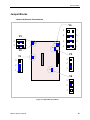
1
Reference
Manual
DOC. REV. 3/19/2009
EBX-22
(Sidewinder)
VIA Eden Based SBC with
Ethernet, Video, Audio, SATA,
Industrial I/O, and SPI
WWW.VERSALOGIC.COM
3888 Stewart Road
Eugene, OR 97402
(541) 485-8575
Fax (541) 485-5712
Contents Copyright © 2009
All Rights Reserved
Notice:
Although every effort has been made to ensure this document is error-free, VersaLogic makes no
representations or warranties with respect to this product and specifically disclaims any implied warranties of
merchantability or fitness for any particular purpose.
VersaLogic reserves the right to revise this product and associated documentation at any time without
obligation to notify anyone of such changes.
PC/104 and the PC/104 logo are trademarks of the PC/104 Consortium.
MEBX-22
EBX-22 Reference Manual
ii
Product Release Notes
Rev 3 Release
Production release.
Rev 2 Release
Beta release. Some functionality has not yet been implemented.
Rev 1 Release
Pre-production only. No customer releases.
Support Page
The EBX-22 support page, at http://www.versalogic.com/private/sidewindersupport.asp, contains
additional information and resources for this product including:
Reference Manual (PDF format)
Operating system information and software drivers
Data sheets and manufacturers’ links for chips used in this product
BIOS information and upgrades
Utility routines and benchmark software
This is a private page for EBX-22 users that can be accessed only be entering this address directly. It cannot
be reached from the VersaLogic homepage.
EBX-22 Reference Manual
iii
Table of Contents
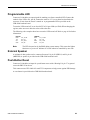
Introduction ..................................................................................................................... 1
Description.......................................................................................................................... 1
Technical Specifications ..................................................................................................... 3
EBX-22 Block Diagram...................................................................................................... 4
CX700M Block Diagram.................................................................................................... 5
RoHS-Compliance .............................................................................................................. 5
About RoHS........................................................................................................... 5
Warnings............................................................................................................................. 6
Electrostatic Discharge .......................................................................................... 6
Lithium Battery...................................................................................................... 6
Mounting Support.................................................................................................. 6
Technical Support ............................................................................................................... 7
Repair Service........................................................................................................ 7
Configuration and Setup ................................................................................................ 8
Initial Configuration ........................................................................................................... 8
Basic Setup ......................................................................................................................... 8
CMOS Setup ..................................................................................................................... 11
Operating System Installation........................................................................................... 16
Physical Details ............................................................................................................. 17
Dimensions and Mounting................................................................................................ 17
Hardware Assembly............................................................................................. 20
Standoff Locations............................................................................................... 20
External Connectors.......................................................................................................... 21
EBX-22 Connectors............................................................................................. 21
EBX-22 Connector Functions and Interface Cables ............................................ 22
CBR-5009 Connectors......................................................................................... 23
CBR-5009 Connector Functions.......................................................................... 23
CBR- 4 004 Connectors........................................................................................ 24
Jumper Blocks................................................................................................................... 25
Jumpers As-Shipped Configuration..................................................................... 25
Jumper Summary ................................................................................................. 26
System Features ........................................................................................................... 27
Power Supply.................................................................................................................... 27
Power Connectors ................................................................................................ 27
Power Requirements ............................................................................................ 27
Lithium Battery.................................................................................................... 28
Voltage Alert Interrupt......................................................................................... 28
CPU................................................................................................................................... 29
System RAM..................................................................................................................... 29
Compatible Memory Modules ............................................................................. 29
CMOS RAM ..................................................................................................................... 29
EBX-22 Reference Manual
iv
Table of Contents
Clearing CMOS RAM ......................................................................................... 29
CMOS Setup Defaults ...................................................................................................... 29
Default CMOS RAM Setup Values..................................................................... 29
Saving CMOS Setup Parameters as Custom Defaults ......................................... 30
Real Time Clock ............................................................................................................... 30
Setting the Clock.................................................................................................. 30
Interfaces and Connectors ........................................................................................... 31
Utility I/O Connectors ...................................................................................................... 31
J14 I/O Connector................................................................................................ 31
J15 I/O Connector................................................................................................ 32
J23 I/O Connector................................................................................................ 33
IDE.................................................................................................................................... 34
SATA Ports....................................................................................................................... 35
Serial Ports........................................................................................................................ 36
COM Port Configuration ..................................................................................... 36
COM3 / COM4 RS-485 Mode Line Driver Control............................................ 36
Serial Port Connectors ......................................................................................... 37
Parallel/Floppy Port .......................................................................................................... 38
Parallel Port Operation......................................................................................... 38
Parallel Port Floppy Disk..................................................................................... 38
PS/2 Keyboard and Mouse ............................................................................................... 39
USB................................................................................................................................... 40
BIOS Configuration............................................................................................. 40
USB Solid State Drive Connector ....................................................................... 40
CompactFlash ................................................................................................................... 41
Installing an Operating System on CompactFlash............................................... 41
Programmable LED .......................................................................................................... 42
External Speaker ............................................................................................................... 42
Push-Button Reset............................................................................................................. 42
Video Interface ................................................................................................................. 43
Configuration ....................................................................................................... 43
Video BIOS Selection.......................................................................................... 43
SVGA Output Connector..................................................................................... 43
LVDS Flat Panel Display Connector................................................................... 44
Compatible LVDS Panel Displays....................................................................... 45
High-Definition Multimedia Interface................................................................. 45
Console Redirection............................................................................................. 46
Ethernet Interface.............................................................................................................. 47
BIOS Configuration............................................................................................. 47
Status LED........................................................................................................... 47
Ethernet Connector .............................................................................................. 48
CPU Temperature Monitor ............................................................................................... 48
Audio ................................................................................................................................ 49
Software Configuration........................................................................................ 49
Watchdog Timer ............................................................................................................... 49
Enabling the Watchdog........................................................................................ 49
Disabling the Watchdog....................................................................................... 49
Refreshing the Watchdog..................................................................................... 50
Watchdog Timer Registers .................................................................................. 50
EBX-22 Reference Manual
v
Table of Contents
Analog Input ..................................................................................................................... 51
External Connections........................................................................................... 51
Calibration ........................................................................................................... 51
Binary Format (0 to +4.095V Only) .................................................................... 52
ADC State Machine ............................................................................................. 52
Analog Input Using the SPI Interface.................................................................. 54
Analog Input “Bit Bang” Register ....................................................................... 55
Digital I/O ......................................................................................................................... 56
External Connections........................................................................................... 56
Digital I/O Port Configuration Using the SPI Interface....................................... 56
Digital I/O “Bit Bang” Register........................................................................... 59
SPI Interface ..................................................................................................................... 61
External Connections........................................................................................... 61
SPI Legacy Mode ................................................................................................ 62
SPI “Bit Bang” Mode .......................................................................................... 65
PWM Outputs and TACH Inputs...................................................................................... 66
External Connections........................................................................................... 66
PWM Output and Tach Input Code Example ...................................................... 66
PC/104 Expansion Bus ..................................................................................................... 69
PC/104 I/O Support ............................................................................................. 69
PC/104 Memory Support ..................................................................................... 69
IRQ Support......................................................................................................... 69
DMA Support ...................................................................................................... 69
System Resources and Maps....................................................................................... 70
Memory Map .................................................................................................................... 70
I/O Map............................................................................................................................. 70
Interrupt Configuration ..................................................................................................... 71
Special Registers .......................................................................................................... 72
Product ID and PLED Register......................................................................................... 72
Revision and Type Register .............................................................................................. 73
Jumper Status Register...................................................................................................... 74
General Purpose Output Register...................................................................................... 74
IRQ and Resource ISA Routing Register ......................................................................... 75
Mode Control Register...................................................................................................... 76
Appendix A – References ............................................................................................. 77
EBX-22 Reference Manual
vi
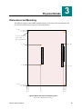
Introduction
1
Description
The EBX-22 is a feature-packed single board computer designed for OEM control projects
requiring fast processing, industrial I/O, flexible memory options and designed-in reliability and
longevity (product lifespan). Its features include:
VIA Eden 1.2 GHz processor
CX700M chipset with integrated
200MHz 128-bit UniChrome Pro
II 2D/3D graphics processor. Up
to 128 MB unified frame buffer:
Four COM ports (two RS-232, two RS232/422/485)
LPT port (floppy mode compatible)
CPU and motherboard temperature sensors
HD audio CODEC, one line in and one line
out only
PS/2 keyboard and mouse ports
Microsoft DirectX 7.0, 8.0 and 9.0
compatible
Support OpenGL
MPEG-2/4 hardware decoding
WMV9 hardware decoding
Integrated HDTV/SDTV encoder
DualView dual image capability
Up to 1 GB system RAM
CompactFlash and USB SSD sites
Dual 10/100 Ethernet interface
Flat panel display support
DVI support through HDMI
connector
Industrial I/O
8-channel, 12-bit analog inputs
32-channel digital I/O
SPI interface supports up to four (external)
SPI devices either of user design or any of
the SPX™ series of expansion boards, with
clock frequencies from 1-8MHz
Watchdog timer
Analog video supports SVGA and
YPbPr (component)
Vcc sensing reset circuit (all rails
monitored, user-selectable interrupt on fault)
EBX-compliant 5.75” x 8.00” footprint
PC/104-Plus expansion site
Two SATA I channels
Field upgradeable BIOS with OEM
enhancements
IDE controller, one channel, ATA
100 compatible
ISA bus, supporting legacy I/O, memory
transactions and IRQs (no DMA or bus
mastering)
Five USB 2.0/1.1 ports
Customizing available
TVS devices (on user I/O
connections)
EBX-22 Reference Manual
1
Introduction
The EBX-22 is compatible with popular operating systems such as Windows and Linux.
A full complement of standard I/O ports are included on-board. Additional I/O expansion is
available through the high-speed PCI-based PC/104-Plus expansion site (which supports both
PC/104 and PC/104-Plus expansion modules), and through the serial peripheral interface (SPI).
A limited ISA bus is created in the PLD to support legacy 8-bit and 16-bit PC/104 ISA cards. It
supports I/O, memory, and interrupts. DMA and bus mastering are not supported.
System memory expansion is supported with one high-reliability latching 240-pin SODIMM
socket. Up to 1 GB of low power, 533 MHz, PC2-4200 compatible DDR2 RAM is available.
The EBX-22 offers a wide range of video and graphics capabilities, including a 2D/3D
UniChrome Pro II graphics processor, high definition MPEG-2/4 processing, high-quality video
that supports RGB555/565/8888 and YUV422 video formats, as well as SVGA, flat panel
display, and a TV interface that supports the YPbPr interface mode.
The EBX-22 features high reliability design and construction. It also features a watchdog timer,
voltage sensing reset circuits and self-resetting fuse on the 5V supply to the keyboard, mouse, and
USB.
All EBX-22 boards are subjected to functional testing and are backed by a limited two-year
warranty. Careful parts sourcing and US-based technical support ensure the highest possible
quality, reliability, service and product longevity for this exceptional SBC.
EBX-22 Reference Manual
2
Introduction
Technical Specifications
Specifications are typical at 25°C with 5.0V supply unless otherwise noted.
Board Size: 5.75" x 8.00" x 1.75"; EBX compliant
Storage Temperature: -40° C to 85° C
Free Air Operating Temperature:
0° C to +60° C EBX-22g
COM3–4 Interface:
RS-232 4-wire, RS-422, RS-485, 16C550
compatible, 460k baud max.
LPT Interface:
Bi-directional/EPP/ECP/floppy mode
compatible
Power Requirements: (with 256 MB DDR2
SODIMM, keyboard and mouse, Windows XP)
EBX-22g – +5.0V ± 5% @ 2.2.0A (11W) typ.
EBX-22h – TBD
+3.3V or ±12V may be required by some
expansion modules
System Reset:
Vcc sensing, resets below 3.3V, 2.5V, or if
Vcore power are not within +/- 10% of
optimal values
Analog Input:
8-channel, 12-bit, single-ended, 500 kSPS,
channel independent input range: 0 to
+4.095V
Digital Interface:
32-channel, ±24 mA source and sink, 3.3V
signaling
SPX Interface:
Supports 4 external SPI chips either of user
design or any of the SPX™ series of
expansion boards
DRAM Interface:
One 240-pin SODIMM socket
Up to 1 GB 533 MHz, PC2-4200 compatible,
DDR2 RAM
Counter/timers:
Three PWM outputs, three TACH inputs
which can be used as general purpose
counter/timers
Video Interface:
Analog outputs for VGA or YPbPr
Digital output, HDMI connector (DVI video
only)
LVDS output for TFT FPDs
Up to 1280 x 1024 (24 bits)
2D/3D MPEG-2/4 graphics
BIOS:
General Software Embedded BIOS© with
OEM enhancements
Field-upgradeable with Flash BIOS Upgrade
Utility
IDE Interface:
One channel, 44-pin keyed 2mm header.
Supports up to UDMA/33.
Supports up to two IDE devices (hard drives,
CD-ROM, CompactFlash, etc.)
SATA Interface:
Two SATA I headers
Ethernet Interface:
Two Intel 82551ER based fast Ethernet
Bus Speed:
CPU Bus: 400 MHz
PC/104-Plus (PCI): 33 MHz
PC/104 (ISA): 8 MHz
Compatibility:
EBX – full compliance
PC/104 (ISA) – limited compliance via PCI to
ISA bridge in PLD
PC/104-Plus) (PCI) – full compliance, 3.3V
signaling, PCI 2.2 compatible
SPX™ – full compliance
10BaseT/100BaseTX controllers
Audio Interface:
HD audio codec, one Line Out and one Line
In support
COM1–2 Interface:
RS-232, 16C550 compatible, 115k baud
max.
Weight:
EBX-22g – 0.606 lbs (0.275 kg)
EBX-22h – TBD
Specifications are subject to change without notice.
EBX-22 Reference Manual
3
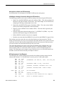
Introduction
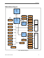
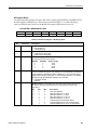
EBX-22 Block Diagram
VIA
Eden
DDR2
SDRAM
VIA
SODIMM
CX700
Chipset
PC/104-Plus
(PCI)
PC/104
(ISA)
10/100 Ethernet
(2)
SPX Interface
PLD
Legacy I/O
Industrial I/O
SVGA Analog
Analog Input
PCI Bus
Digital I/O 0-15
SPI
Host Bus
CPU
Digital I/O 16-31
LVDS Flat Panel
USB 4
HDMI
J5
CBR-4004
I/O
Connector
J23
CBR-4004
I/O
Connector
LPC Bus
Audio Codec
SATA 1
COM 1-2
RS-232
LPC
Super I/O
SATA 2
COM 3-4
RS-232/422/485
J14
CBR-5009
I/O
Connector
PS/2 Mouse /
Keyboard
USB 0-3
LPT/Floppy
Speaker
Digital Video
Input/Output
USB 5 SSD
PLED
IDE
Reset
CompactFlash
External Wake
Figure 1. EBX-22 Block Diagram
EBX-22 Reference Manual
4
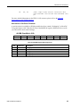
Introduction
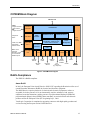
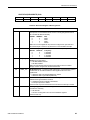
CX700M Block Diagram
VIA Eden CPU
LVDS:
2 single-channels,
1 dual-channel
DVI:
1 single-channel
LVDS/DVI
Transmitter
Component
Video
Video DACs
LVDS, DVI, HDMI
Transmitter/
HDTV Encoder
VCP: 1 8-bit
Transport
Streams/ 1 16-bit
or 2 8-bit CCIR656/601 Inputs
Digital Video
Port 1
Video Capture
Port
Host Interface
HDTV
Encoder
2D GFX Processor
3D GFX Processor
Unified Video Decoding
Accelerator – MPEG-2/4 and
WMV9 video acceleration
Hi-Def Video
Processor
PCI
HD
Audio
4 Master
Devices
RTC & CMOS
RAM
MC97
MC’97
Codec
HD Audio
Codec
Power
Management
ECC
DRAM
Controller
PS/2
SMBUS
LPC
1 Master +
1 Slave
Keyboard
+ Mouse
EIDE/
UARTS
2 EIDE
Devices/
2 UARTs
LPC
Devices
(e.g. Super I/O)
USB
2.0
SATA
2 Ports
6 Ports
DDR2
SDRAM
Figure 2. CX700M Block Diagram
RoHS-Compliance
The EBX-22 is RoHS-compliant.
ABOUT ROHS
In 2003, the European Union issued Directive 2002/95/EC regarding the Restriction of the use of
certain Hazardous Substances (RoHS) in electrical and electronic equipment.
The RoHS directive requires producers of electrical and electronic equipment to reduce to
acceptable levels the presence of six environmentally sensitive substances: lead, mercury,
cadmium, hexavalent chromium, and the presence of polybrominated biphenyls (PBB) and
polybrominated diphenyl ethers (PBDE) flame retardants, in certain electrical and electronic
products sold in the European Union (EU) beginning July 1, 2006.
VersaLogic Corporation is committed to supporting customers with high-quality products and
services meeting the European Union’s RoHS directive.
EBX-22 Reference Manual
5
Introduction
Warnings
ELECTROSTATIC DISCHARGE
Electrostatic discharge (ESD) can damage boards, disk drives and other components. The circuit
board must only be handled at an ESD workstation. If an approved station is not available, some
measure of protection can be provided by wearing a grounded antistatic wrist strap. Keep all
plastic away from the board, and do not slide the board over any surface.
After removing the board from its protective wrapper, place the board on a grounded, static-free
surface, component side up. Use an antistatic foam pad if available.
The board should also be protected inside a closed metallic anti-static envelope during shipment
or storage.
Note
The exterior coating on some metallic antistatic bags is sufficiently conductive to
cause excessive battery drain if the bag comes in contact with the bottom-side of
the EBX-22.
LITHIUM BATTERY
To prevent shorting, premature failure or damage to the lithium battery, do not place the board on
a conductive surface such as metal, black conductive foam or the outside surface of a metalized
ESD protective pouch. The lithium battery may explode if mistreated. Do not recharge,
disassemble or dispose of in fire. Dispose of depleted batteries promptly.
MOUNTING SUPPORT
The single board computer must be supported at all eight mounting points to prevent excessive
flexing when expansion modules are mated and detached. Flex damage caused by excessive force
on an improperly mounted circuit board is not covered under the product warranty. See page 17
for more details.
EBX-22 Reference Manual
6
Introduction
Technical Support
If you are unable to solve a problem with this manual please visit the EBX-22 Product Support
web page listed below. If you have further questions, contact VersaLogic technical support at
(541) 485-8575. VersaLogic technical support engineers are also available via e-mail at
Support@VersaLogic.com.
EBX-22 Support Website
http://www.versalogic.com/private/Sidewindersupport.asp
REPAIR SERVICE
If your product requires service, you must obtain a Returned Material Authorization (RMA)
number by calling (541) 485-8575.
Please provide the following information:
Your name, the name of your company and your phone number
The name of a technician or engineer that can be contact if any questions arise.
Quantity of items being returned
The model and serial number (barcode) of each item
A detailed description of the problem
Steps you have taken to resolve or recreate the problem
The return shipping address
Warranty Repair
All parts and labor charges are covered, including return shipping
charges for UPS Ground delivery to United States addresses.
Non-warranty Repair All non-warranty repairs are subject to diagnosis and labor charges,
parts charges and return shipping fees. Please specify the shipping
method you prefer and provide a purchase order number for invoicing
the repair.
Note
EBX-22 Reference Manual
Please mark the RMA number clearly on the outside of the box before
returning. Failure to do so can delay the processing of your return.
7
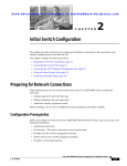
Configuration and Setup
2
Initial Configuration
The following components are recommended for a typical development system. Note that this is a
recommended configuration only.
Note
You may substitute other components for the ones listed below, such as a PS/2
mouse and keyboard, a parallel ATA hard drive or CD-ROM drive, or another type
of monitor. If you substitute other components, be sure to adjust the basic setup
steps accordingly.
EBX-22 single board computer
240-pin SODIMM (memory module): DDR2-400 or DDR2-533
ATX power supply with motherboard and drive connectors
SVGA video monitor
USB keyboard and mouse
SATA hard drive
USB CD-ROM drive
The following VersaLogic cables are recommended.
Video adapter cable (CBR-1201)
SATA data cable (CBR-0701)
ATX to SATA power adapter cable (CBR-0401)
Power adapter cable (CBR-2022)
You will also need a Windows (or other OS) installation CD.
Basic Setup
The following steps outline the procedure for setting up a typical development system. The EBX22 should be handled at an ESD workstation or while wearing a grounded antistatic wrist strap.
Before you begin, unpack the EBX-22 and accessories. Verify that you received all the items you
ordered. Inspect the system visually for any damage that may have occurred in shipping. Contact
Support@VersaLogic.com immediately if any items are damaged or missing.
Gather all the peripheral devices you plan to attach to the EBX-22 and their interface and power
cables.
It is recommended that you attach standoffs to the board (see Hardware Assembly) to stabilize the
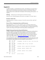
board and make it easier to work with.
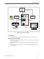
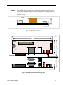
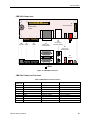
Figure 3 shows a typical start-up configuration.
EBX-22 Reference Manual
8
Configuration and Setup
ATX
Power
Supply
CBR– 0401
CBR– 2022
CD-ROM
Drive
USB
OS Installation
CD-ROM
USB
J6
EBX-22
SATA
Hard Drive
“Sidewinder”
J4 J11
J3 J9
J10
J8
CBR– 0701
J7
USB Keyboard
and Mouse
CBR– 1201
Analog SVGA
Figure 3. Typical Start-up Configuration
1. Install Memory
Insert the DDR2 DRAM module into the SODIMM socket J2 and latch it into place.
2. Attach Cables and Peripherals
Plug the video adapter cable CBR-1201 into socket J7. Attach the video monitor interface
cable to the video adapter.
Plug the USB CD-ROM drive, keyboard, and mouse into on-board USB sockets (J3, J4,
J9, or J11).
Plug the SATA data cable CBR-0701 into socket J8 or J10, and attach the SATA hard
drive to the cable.
EBX-22 Reference Manual
9
Configuration and Setup
Note
The mating connector on some SATA data cables may interfere with the
proper seating of a PC/104-Plus (PCI) expansion board at connector J17.
The SATA specification does not specify exterior dimensions for
connector housings, and some manufacturers make wider housings than
others. The 3M 5602 Series straight SATA connector is 0.22 in. wide and
will interfere less with the PC/104-Plus card. Even with thinner SATA
cables, you may need to ease the cable(s) away from the PC/104-Plus
connector to seat the expansion board completely.
Attach an ATX power cable to the SATA hard drive.
3. Attach Power
Plug the power adapter cable CBR-2022 into connector J6. Attach the motherboard
connector of the ATX power supply to the adapter.
4. Soft Power Button Configuration
The EBX-22 requires activation of the soft power button to power up. This can be
executed manually or automatically. Installing a jumper on pins V5[1-2] causes the EBX22 to create its own soft power pulse automatically when power is applied. If a jumper is
installed at V5[3-4], you will have to create a pulse on pin 40 of I/O connector J14. This
can be done by shorting pin 40 to ground for 100 to 500 ms.
5. Review Configuration
Before you power up the system, double check all the connections. Make sure all cables
are oriented correctly and that adequate power will be supplied to the EBX-22 and
peripheral devices.
Verify that jumper V1[1-2] is installed. This connects the battery to the 32 kHz clock and
CMOS. The board will not turn on with out this connection.
6. Power On
Turn on the ATX power supply and the video monitor. If the system is correctly
configured, a video signal should be present.
7. Select a Boot Drive
During startup, press the B key to display the boot menu. Insert the OS installation CD in
the CD-ROM drive, and select to boot from the CD-ROM drive.
8. Install Operating System
Note
Install the operating system according to the instructions provided by the OS
manufacturer. (See Operating System Installation.)
If you intend to operate the EBX-22 under Windows XP or Windows XP
Embedded, be sure to use Service Pack 2 (SP2) and all updates for full support of
the latest hardware features.
EBX-22 Reference Manual
10
Configuration and Setup
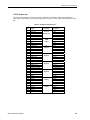
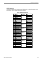
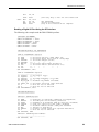
CMOS Setup
The default CMOS Setup parameters for the EBX-22 are shown below. Due to changes and
improvements in the system BIOS, the information on your monitor may differ from that shown
below. The factory default date will correspond to the BIOS build date. Some values may vary
depending on the configuration of your EBX-22.
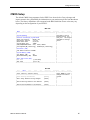
Main Tab
+
|
|
|
|
|
|
|
|
|
|
|
|
|
|
|
|
|
|
|
|
|
+
Main
Exit
Boot
POST
SIO
Features
Firmbase
Misc
Board
------------------------------------------------------ + ------------------- +
|
|
System Summary
|Use TAB to switch
|
------------------------------------------------------ |between month, day
|
General Software[R] System BIOS
|and year. Use digits|
BIOS Core Version
EB(SF).003
|and BKSP to change
|
VersaLogic Version
6.3.102
|field.
|
BIOS Build Date
03/19/08
|
|
System BIOS Size
128KB
|
|
CPM/CSPM/BPM Modules P7C7, CX700, EBX22
|
|
StrongFrame[TM] Technology, Firmbase[R] Technology
|
|
|
|
Processor (CPU)
|
|
VIA Eden Processor 1200MHz
|
|
|
|
System Memory (RAM)
|
|
Low Memory (KB)
627
|
|
Extended Memory (KB) 449344
|
|
|
|
Real Time Clock (RTC)
|
|
RTC Date
[03/26/2008]
|
|
RTC Time
[13:57:20]
|
|
------------------------------------------------------ + ------------------- +
Exit Tab
+
|
|
|
|
|
|
|
|
|
+
Main
Exit
Boot
POST
SIO
Features
Firmbase
Misc
Board
------------------------------------------------------ + ------------------Save, Restore, and Exit Setup
|Press ENTER to save
------------------------------------------------------ |changes and reboot
Save Settings and Restart
[Enter]
|system.
|
Exit Setup Without Saving Changes
[Enter]
|
|
Reload Factory-Defaults and Restart
[Enter]
|
|
Reload Custom-Defaults and Restart
[Enter]
|
------------------------------------------------------ + -------------------
EBX-22 Reference Manual
+
|
|
|
|
|
|
|
|
|
+
11
Configuration and Setup
Boot Tab
+
|
|
|
|
|
|
|
|
|
|
|
|
|
|
|
|
|
|
|
|
|
|
|
|
|
|
+
Main
Exit
Boot
POST
SIO
Features
Firmbase
Misc
Board
------------------------------------------------------ + ------------------- +
System Boot Configuration
|Select initialization|
------------------------------------------------------ |and boot priority for|
|all devices.
|
Boot Device Prioritization (BBS)
|
|
0 [IDE 2/ATA Master]
|Backspace deletes
|
1 [None]
|selection. Space
|
|bar, + and - change |
Initialization Policy [All Devices]
|selections.
|
|
|
Floppy Drive Configuration
|
|
Floppy 0
[1.44 MB, 3.5]
|
|
|
|
IDE Drive Configuration
|
|
IDE 0 Type
[Autoconfig]
|
|
IDE 0 Mode
[UDMA mode (80-conductor cable)]
|
|
IDE 1 Type
[Autoconfig]
|
|
IDE 1 Mode
[UDMA mode (80-conductor cable)]
|
|
IDE 2 Type
[Autoconfig]
|
|
IDE 2 Mode
[UDMA mode (40-conductor cable)]
|
|
IDE 3 Type
[Autoconfig]
|
|
IDE 3 Mode
[UDMA mode (40-conductor cable)]
|
|
|
|
VT8237 ATA Controller Configuration
|
|
-------------------------------------------------------|
|
PATA Controller
[Compatible Mode]
|
|
SATA Controller
[Native Mode]
|
|
------------------------------------------------------ + ------------------- +
POST Tab
+
|
|
|
|
|
|
|
|
|
|
|
|
|
|
|
|
|
|
|
|
|
|
|
|
|
|
|
+
Main
Exit
Boot
POST
SIO
Features
Firmbase
Misc
Board
------------------------------------------------------ + ------------------- +
POST Memory Tests
|Enable basic memory |
------------------------------------------------------ |confidence test below|
Low Memory Standard Test
[Disabled]
|1MB during POST.
|
Low Memory Exhaustive Test
[Disabled]
|
|
High Memory Standard Test
[Disabled]
|
|
High Memory Exhaustive Test
[Disabled]
|
|
Click During Memory Test
[Disabled]
|
|
Clear Memory During Test
[Disabled]
|
|
|
|
POST Error Control
|
|
------------------------------------------------------ |
|
|
|
POST User Interface
|
|
------------------------------------------------------ |
|
POST Display Messages
[Enabled]
|
|
POST Operator Prompt
[Enabled]
|
|
POST Display PCI Devices
[Enabled]
|
|
|
|
POST Debugging
|
|
------------------------------------------------------ |
|
Post Slow Reboot Cycle
[Disabled]
|
|
POST Fast Reboot Cycle
[Disabled]
|
|
|
|
Device Initialization
|
|
------------------------------------------------------ |
|
POST Floppy Seek
[Disabled]
|
|
POST Hard Disk Seek
[Enabled]
|
|
------------------------------------------------------ + ------------------- +
EBX-22 Reference Manual
12
Configuration and Setup
SIO Tab
+
|
|
|
|
|
|
|
|
|
|
|
|
|
|
|
|
|
|
|
|
|
|
|
|
+
Main
Exit
Boot
POST
SIO
Features
Firmbase
Misc
Board
------------------------------------------------------ + ------------------BIOS Super I/O Configuration
|
------------------------------------------------------ |
|
SCH3114 Devices
|
------------------------------------------------------ |
Parallel Port (J29)
[Enabled]
|
Address
[378h]
|
IRQ
[IRQ 7]
|
DMA
[Channel 4]
|
Mode
[Printer]
|
Serial Port 1 (J3 Top)
[Enabled]
|
Address
[3f8h]
|
IRQ
[IRQ 4]
|
Serial Port 2 (J3 Bot)
[Enabled]
|
Address
[2f8h]
|
IRQ
[IRQ 3]
|
Serial Port 3 (J6)
[Disabled]
|
Address
[3e8h]
|
IRQ
[No IRQ]
|
Mode
[RS-232 (4-wire)]
|
Serial Port 4 (J5)
[Disabled]
|
Address
[2e8h]
|
IRQ
[No IRQ]
|
Mode
[RS-232 (4-wire)]
|
------------------------------------------------------ + -------------------
+
|
|
|
|
|
|
|
|
|
|
|
|
|
|
|
|
|
|
|
|
|
|
+
Main
Exit
Boot
POST
SIO
Features
Firmbase
Misc
Board
------------------------------------------------------ + ------------------- +
BIOS Feature Configuration
|Enable to initialize |
------------------------------------------------------ |APICs and use them in|
Interrupt Processing
[Use APIC]
|an emulated PIC mode.|
Quick Boot
[Enabled]
|If you wish to use
|
Advanced Power Management
[Disabled]
|full-APIC mode, this |
ACPI
[Enabled]
|must be set AND
|
POST Memory Manager
[Disabled]
|either ACPI or MP
|
System Management BIOS
[Enabled]
|must be enabled. DO |
Manufacturing Mode
[Disabled]
|NOT CHANGE AFTER OS |
Splash Screen
[Disabled]
|INSTALL.
|
|
|
Console Redirection
|
|
------------------------------------------------------ |
|
Use Console Assignments Below [On Remote User Detect] |
|
POST Console
[COM1]
|
|
Preboot Console
[COM1]
|
|
Debugger Console
[COM1]
|
|
|
|
CPU Configuration
|
|
------------------------------------------------------ |
|
CPU Speed
[1200 MHz]
|
|
Microcode Update
[Enabled]
|
|
------------------------------------------------------ + ------------------- +
+
|
|
|
|
|
|
|
|
|
|
|
|
|
|
|
|
|
|
|
|
|
|
|
|
+
Features Tab
EBX-22 Reference Manual
13
Configuration and Setup
Firmbase Tab
+
|
|
|
|
|
|
|
|
|
|
|
|
|
|
|
|
|
|
|
|
|
|
|
|
|
+
Main
Exit
Boot
POST
SIO
Features
Firmbase
Misc
Board
------------------------------------------------------ + ------------------- +
Features Enabled by Firmbase[R] Technology
|Enable to support USB|
------------------------------------------------------ |keyboard and mouse
|
Legacy USB
[Enabled]
|
|
USB Boot
[Enabled]
|
|
EHCI/USB 2.0
[Enabled]
|
|
Firmbase Disk I/O
[Disabled]
|
|
|
|
Basic Firmbase[R] Technology Configuration
|
|
------------------------------------------------------ |
|
Firmbase Technology
[Enabled]
|
|
Firmbase Debug Log
[None]
|
|
Firmbase System Console
[None]
|
|
Firmbase Shell on Serial Port [None]
|
|
Quiet Mode
[Disabled]
|
|
Strict Mode
[Enabled]
|
|
Bypass Mode
[Enabled]
|
|
TCB Security
[Enabled]
|
|
Statistics
[Enabled]
|
|
Clear Memory
[Disabled]
|
|
Use TSC
[Enabled]
|
|
Timer Optimization
[Disabled]
|
|
Debug Yields
[Disabled]
|
|
|
|
...
|
|
|
|
------------------------------------------------------ + --------------------+
Note: It is strongly advised that settings on this tab beyond the Basic Firmbase Technology
Configuration section not be changed.
Misc Tab
+
|
|
|
|
|
|
|
|
|
|
|
|
|
|
|
|
|
+
-----------------------------------------------------Cache Control
-----------------------------------------------------CPU Cache
[Enabled]
System Cache
[Enabled]
+ ------------------|Enable to allow CPU
|level cache to
|operate.
|
|
Keyboard Control
|
------------------------------------------------------ |
Keyboard Numlock LED
[Disabled]
|
Typematic Rate
[30/sec]
|
Typematic Delay
[250ms]
|
|
Miscellaneous BIOS Configuration
|
------------------------------------------------------ |
Lowercase Hex Displays
[Disabled]
|
|
|
|
------------------------------------------------------ + -------------------
EBX-22 Reference Manual
+
|
|
|
|
|
|
|
|
|
|
|
|
|
|
|
|
|
+
14
Configuration and Setup
Board Tab
+
|
|
|
|
|
|
|
|
|
|
|
|
|
|
|
|
|
|
|
|
|
|
|
|
|
+
Main
Exit
Boot
POST
SIO
Features
Firmbase
Misc
Board
------------------------------------------------------ + ------------------Flash Protection
[Enabled]
|Write-protect Flash
|BIOS sectors.
PCI Interrupt Configuration
|
------------------------------------------------------ |
PCI INT A routing
[IRQ 11]
|
PCI INT B routing
[IRQ 11]
|
PCI INT C routing
[IRQ 11]
|
PCI INT D routing
[IRQ 9]
|
|
ISA Interrupt Configuration
|
------------------------------------------------------ |
ISA IRQ 3
[Disabled]
|
ISA IRQ 4
[Disabled]
|
ISA IRQ 5
[Disabled]
|
ISA IRQ 10
[Disabled]
|
|
Hardware Monitoring Interrupt Configuration
|
-------------------------------------------------------|
Voltage IRQ enable
[Disabled]
|
Overtemp IRQ enable
[Disabled]
|
CPU overtemp threshold, *C
[95]
|
Board overtemp threshold, *C [60]
|
Voltage or Temperature IRQ
[None]
|
|
|
------------------------------------------------------ + -------------------
+
|
|
|
|
|
|
|
|
|
|
|
|
|
|
|
|
|
|
|
|
|
|
|
|
|
+
Chipset Tab
+
|
|
|
|
|
|
|
|
|
|
|
|
|
|
|
|
|
|
|
|
|
+
Boot
POST
SIO
Features
Firmbase
Misc
Board
Chipset
------------------------------------------------------ + ------------------|Select video output
Display Device Configuration
|device.
------------------------------------------------------ |Some modes may
Video Output Device
[VGA]
|require a different
LCD Device Type
[1]
|Video BIOS support.
Expansion/Centering
[Expansion]
|
DVI Connector
[Present]
|
TV Output Connector
[Component 0 (YPbPr)]
|
TV Output Format
[NTSC]
|
|
Memory Configuration
|
------------------------------------------------------ |
DQS Input Delay Control
[Auto]
|
DQS Input Delay
[13]
|
|
CX700 Chipset Feature Configuration
|
------------------------------------------------------ |
Video Frame Buffer Size
[64 MB]
|
AGP Aperture Size
[128 MB]
|
|
|
------------------------------------------------------ + -------------------
EBX-22 Reference Manual
+
|
|
|
|
|
|
|
|
|
|
|
|
|
|
|
|
|
|
|
|
|
+
15
Configuration and Setup
Status Tab
POST
SIO
Features
Firmbase
Misc
Board
Chipset
Status
+--------------------------------------------------------+---------------------+
|
|
|
| CPU Real-Time Statistics
|
|
| -------------------------------------------------------|
|
| Thermal Diode Reading, Current *C:
50
|
|
|
|
|
|
|
|
+--------------------------------------------------------+---------------------+
Operating System Installation
The standard PC architecture used on the EBX-22 makes the installation and use of most of the
standard x86 processor-based operating systems very simple. The operating systems listed on the
VersaLogic OS Compatibility Chart use the standard installation procedures provided by the
maker of the OS. Special optimized hardware drivers for a particular operating system, or a link
to the drivers, are available at the EBX-22 Product Support web page at
http://www.versalogic.com/private/Sidewindersupport.asp.
Note
An operating system installed on a different type of computer is not guaranteed to
work on the EBX-22. This is referred to as a “foreign” installation. A hard disk that
was used to boot a different computer cannot necessarily be moved to the EBX-22
and expected to boot. Even when porting an OS image from one revision of the
EBX-22 to another, performance might fail or be impaired. For the best results,
perform a fresh installation of the OS on each system. This restriction does not
apply if you are producing multiple identical systems.
EBX-22 Reference Manual
16
Physical Details
3
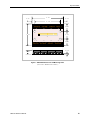
Dimensions and Mounting
The EBX-22 complies with all EBX standards which provide for specific mounting hole and
PC/104-Plus stack locations as shown in the diagram below.
7.80
7.60
0.125 DIA x8
Use 3mm or
#4 standoffs
5.80
5.70
2.80
2.65
0.00
5.25
5.35
5.55
1.875
–0.20
0.00
-0.20
Figure 4. EBX-22 Dimensions and Mounting Holes
(Not to scale. All dimensions in inches.)
EBX-22 Reference Manual
17
Physical Details
Caution
The EBX-22 must be supported at all eight mounting points to prevent excessive
flexing when expansion modules are mated and demated. Flex damage caused by
excessive force on an improperly mounted circuit board is not covered under the
product warranty.
Heatsink
0.85
0.06
Figure 5. EBX-22 Height Dimensions
(Not to scale. All dimensions in inches.)
5.50
5.10
1.575
1.87
1.9
1.175
1.325
0.06
Figure 6. CBR-5009 Dimensions and Mounting Holes
(Not to scale. All dimensions in inches.)
EBX-22 Reference Manual
18
Physical Details
2.87
0.25
0.25
2.38
0.70
J1
J2
J3
J4
+
+
1.95
0.63
J5
+
+
J6
J7
J8
J9
0.62
0.06
0.40
Figure 7. CBR-4004 Dimensions and Mounting Holes
(Not to scale. All dimensions in inches.)
EBX-22 Reference Manual
19
Physical Details
HARDWARE ASSEMBLY
The EBX-22 mounts on four hardware standoffs using the corner mounting holes (A). These
standoffs are secured to the underside of the circuit board using pan head screws.
Four additional standoffs (B) must be used under the circuit board to prevent excessive flexing
when expansion modules are mated and separated. These are secured with four male-female
standoffs (C), threaded from the top side, which also serve as mounting struts for the PC/104
stack.
The entire assembly can sit on a table top or be secured to a base plate. When bolting the unit
down, make sure to secure all eight standoffs (A and B) to the mounting surface to prevent circuit
board flexing.
An extractor tool is available (part number VL-HDW-201) to separate the PC/104 modules from
the stack.
Note
Standoffs and screws are available as part number VL-HDW-101.
STANDOFF LOCATIONS
C
B
A
Figure 8. Standoff Locations
EBX-22 Reference Manual
20
Physical Details
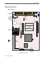
External Connectors
EBX-22 CONNECTORS
J15
Analog, PWM,
Digital I/O
J29
LPT
V3
V2
J14
COM 1-4,
PLED, PS/2
Keyboard and
Mouse, Reset
Button,
Speaker
J23
Audio, Digital
I/O, USB 4
J6
Power
J22
IDE
V6
J25
SPI
V5
J13
USB SSD
J26-27
PC/104
(ISA)
Battery
J17
PC/104-Plus
(PCI)
J10
SATA 2
V1
J20
CompactFlash
J5 Ethernet 1
J12 Ethernet 0
J4
J11
USB 3
USB 1
J3
J9
USB 2
USB 0
J8
SATA 1
V4
= Pin 1
= Key
J2
SODIMM
Memory
CPU
J7
SVGA
J16
Fan
J19 LVDS
J24
HDMI
Figure 9. EBX-22 Connectors
EBX-22 Reference Manual
21
Physical Details
EBX-22 CONNECTOR FUNCTIONS AND INTERFACE CABLES
The following table notes the function of each connector, as well as mating connectors and
cables, and the page where a detailed pinout or further information is available.
Table 1: Connector Functions and Interface Cables
Connector
1
Function
Mating Connector
J2
Memory
DDR2 DRAM
–
–
29
J3
USB 2
USB Series A Plug
–
–
40
J4
USB 3
USB Series A Plug
–
–
40
J5
Ethernet 1
RJ45 Crimp-on Plug
–
–
47
J6
Main Power Input
(EBX Compliant)
SVGA Video
Output
SATA 1
Molex 39-01-2100
Molex 39-00-0059 (10 ea.)
FCI 89361-712LF or
FCI 89947-712LF
Standard SATA
CBR-2022
6” ATX to EPIC power
cable
1’ 12-pin 2mm IDC to
15-pin HD D-Sub VGA
500mm (19.75”) 7-pin,
straight-to-straight
SATA data ; ATX to
SATA power adapter
–
27
35
J7
J8
Cable
CBR-1201
CBR-0701;
CBR-0401
Cable Description
Page
43
35
J9
USB 0
USB Series A Plug
–
J10
SATA 2
Standard SATA
CBR-0701;
CBR-0401
J11
USB 1
USB Series A Plug
–
500mm 7-pin, straight to
straight SATA data; ATX
to SATA power adapter
–
J12
Ethernet 0
RJ45 Crimp-on Plug
–
–
47
J13
Intel Z-U130 SSD, 2mm
socket
FCI 89361-350LF
_
_
40
CBR-5009A
18” 2mm 50-pin to 50pin IDC to breakout
board CBR-5009B
31
FCI 89361-340LF
CBR-4004A
–
–
12” 2mm 40-pin to 40pin IDC to CBR-4004B
board
Fan power cable with 2pin connector
32
J16
USB Solid State
Drive
COM 1-4, PLED,
PS/2 Keyboard
and Mouse, Reset
Button, Speaker,
External Wake
Digital I/O 0-15,
A/D 0-7, Reset,
PLD, PWM 1-3
CPU Fan
J17
PC-104-Plus
AMP 1375799-1
–
–
69
J19
LVDS
20-pin, PanelMate 1.25mm CBR-2010
or
CBR-2011
44
J20
CompactFlash
J22
IDE Hard Drive
Type I or Type II
Compact Flash
FCI 89947-144LF
18-bit TFT FPD using
20-pin Hirose
18-bit TFT FPD using
20-pin JAE
–
J23
USB 4, Digital I/O
16-31, Audio
J14
J15
–
CBR-4406
2
CBR-4405
CBR-4004A
40
40
–
40
J24
HDMI
Standard HDMI
–
18” 2mm IDE cable
2mm to 0.1” adapter
12” 2mm 40-pin to 40pin IDC to CBR-4004B
board
19-pin HDMI, video only
J25
SPI
FCI 89361714LF
CBR-1401 or
CBR-1402
2mm 14-pin IDC, 2 or 4
SPX device cable
PC/104
AMP 1375795-2
–
–
69
LPT/Floppy
FCI 89361720LF
CBR-2003
12” 2mm 20-pin IDC
LPT
38
J26, J27
J29
FCI 89361-340LF
34
40
45
1. Connectors J1 and J28 are for factory use only. Connectors J18 and J21 are not installed.
2. CBR-4405 44-pin to 40-pin adapter is required to connect to 3.5-inch IDE drives with 40-pin connectors.
EBX-22 Reference Manual
22
Physical Details
CBR-5009 CONNECTORS
1
2
49
50
J2
Soft Power Button
J1
Breakout Board
Adapter
5
1
1
5
SP1
J5
Speaker COM4
1
5
J6
COM3
J3
COM1 (Top)
COM2 (Bottom)
J4
PS/2
Mouse (Top)
Keyboard (Bottom)
D1
Power (Top)
PLED (Bottom)
S1
Reset
= Pin 1
Figure 10. CBR-5009 Connectors
CBR-5009 CONNECTOR FUNCTIONS
Table 2: CBR-5009 Connector Functions
Connector /
Component
Function
Part Number
Description
D1
Power and Programmable LEDs
Dialight 552-0211
LEDx2 T1 3/4 PC Mount Red/Red
J1
High Density Connector
FCI 98414-F06-50U
2mm, 50 pins, keyed, latching header
J2
Soft Power Button Input
Conta-Clip 10250.4
5 pin screw terminal
J3
COM1, COM2
Kycon K42-E9P/P-A4N
Dual stacked DB-9 male
J4
PS/2 Keyboard and Mouse
Kycon KMDG-6S/6S-S4N
Dual stacked PS/2 female
J5
COM4
Conta-Clip 10250.4
5 pin screw terminal
J6
COM3
Conta-Clip 10250.4
5 pin screw terminal
S1
Reset Button
E-Switch 800SP9B7M6RE
Right angle momentary switch
Speaker
Challenge Electronics DBX05
Miniature PC speaker
SP1
EBX-22 Reference Manual
23
Physical Details
CBR- 4 004 CONNECTORS
J1
5
J2
1
5
J3
1
5
J4
1
5
1
40
39
2
1
J5
1
5
J6
1
5 1
J7
5
1
J8
5
J9
= Pin 1
Figure 11. CBR-4004 Connectors
CBR-4004 connector functions depend on the I/O connector to which it is attached, J15 or J23.
See Table 6 (J15) or Table 7 (J23) for details.
EBX-22 Reference Manual
24
Physical Details
Jumper Blocks
JUMPERS AS-SHIPPED CONFIGURATION
V6
V3
2
2
1
1
V3
V2
8
7
6
5
4
3
2
1
V6
V5
V2
V1
V5
V1
3
3
2
2
1
V4
1
V4
1
2
3
Figure 12. Jumper Block Locations
EBX-22 Reference Manual
25
Physical Details
JUMPER SUMMARY
Table 3: Jumper Summary
Jumper
Block
V1
V2[1-2]
V3[3-4]
V4
V5
V6[1-2]
V6[3-4]
V6[5-6]
V6[7-8]
Description
CMOS RAM and Real Time Clock Erase
[1-2] In – Normal
[2-3] In – Erase CMOS RAM and real-time clock
COM3 RS-485 Termination
In – 100 Ohm terminated
Out – COM3 Not terminated
COM4 RS-485 Termination
In – 100 Ohm terminated
Out – COM4 Not terminated
CRT and TV Select
[1-2] In – CRT
[2-3] In – TV
Reset Select
[1-2] In – Generated
[2-3] In – Power button
The EBX-22 requires activation of the soft power button to power up.
Installing a jumper on pins [1-2] causes the EBX-22 to create its own
soft power pulse automatically when power is applied. See page 10 for
details.
CompactFlash Master Selector
In – CompactFlash module is IDE master
Out – CompactFlash module is IDE slave
Video BIOS Selector
In – Primary video BIOS selected
Out – Secondary video BIOS selected
The secondary video BIOS is field-upgradeable using the FBU utility.
See the EBX-22 support page for more information.
Reserved
In – Normal operation
Out – Factory use only
This jumper should not be removed. If you hear a low-high beep tone
and the EBX-22 appears to be failing to boot, verify that this jumper is
properly installed.
Reserved
EBX-22 Reference Manual
As
Shipped
Page
[1-2] In
29
(Normal)
In
36
In
36
[1-2] In
43
(CRT)
[1-2] In
–
(Generated)
In
41
In
43
In
–
–
–
26
System Features
4
Power Supply
POWER CONNECTORS
Main power is applied to the EBX-22 through an EPIC-style 10-pin polarized connector at
location J6.
Warning!
To prevent severe and possibly irreparable damage to the system, it is critical that
the power connectors are wired correctly. Make sure to use both +5VDC pins and
all ground pins to prevent excess voltage drop.
Table 4: Main Power Connector Pinout
Note
J6
Pin
Signal
Name
Description
1
PS_ON
Soft Power Off
2
GND
Ground
3
GND
Ground
4
+12VDC
Power Input
5
+3.3VDC
Power Input
6
+5VSB
5V Standby
7
+5VDC
Power Input
8
+5VDC
Power Input
9
-12VDC
Power Input
10
GND
Ground
The +3.3VDC, +12VDC and -12VDC inputs on the main power connector are only
required for PC/104-Plus and PC/104 expansion modules that require these
voltages.
POWER REQUIREMENTS
The EBX-22 requires only +5.0 volts (±5%) for proper operation. The voltage required for the
RS-232 ports and analog input sections are generated with a DC/DC converter. Low-voltage
supply circuits provide power to the CPU and other on-board devices.
The exact power requirement of the EBX-22 depends on several factors, including memory
configuration, CPU speed, peripheral connections, type and number of expansion modules and
attached devices. For example, PS/2 keyboards typically draw their power directly from the EBX22, and driving long RS-232 lines at high speed can increase power demand.
EBX-22 Reference Manual
27
System Features
LITHIUM BATTERY
Warning!
To prevent shorting, premature failure or damage to the lithium battery, do not
place the board on a conductive surface such as metal, black conductive foam or
the outside surface of a metalized ESD protective pouch. The lithium battery may
explode if mistreated. Do not recharge, disassemble or dispose of in fire. Dispose
of used batteries promptly.
Normal battery voltage should be at least 3.0V. If the voltage drops below 3.0V, contact the
factory for a replacement (part number HB3/0-1). The life expectancy under normal use is
approximately 10 years.
VOLTAGE ALERT INTERRUPT
The EBX-22 can be configured to generate an interrupt if the 5V power rail exceeds 5.25V or
drops below 4.75V. These voltage thresholds conform to the power supply recommendation of
5V +/- 5%. The voltage alert interrupt is enabled in CMOS Setup on the Board tab. Interrupts
available for this purpose are IRQ 3, 4, 5, and 10. (The NMI, non-maskable interrupt, setting is
reserved for future use).
Note:
The IRQ for voltage and temperature monitoring is shared. When the Voltage or
Temperature IRQ option is set, the selected IRQ will apply to both voltage and
temperature monitoring if they are enabled.
EBX-22 Reference Manual
28
System Features
CPU
The VIA Eden is an extremely low power consumption (7W at 1 GHz) x86 microprocessor with a
maximum operating frequency of 1.2 GHz and bus speeds up to 800 mega-transfers per second
(MT/s). The VIA Eden features two 64 KB Level 1 caches, one 128 KB Level 2 cache, and
DDR2 SDRAM support.
System RAM
COMPATIBLE MEMORY MODULES
The EBX-22 accepts one 240-pin SODIMM memory module with the following characteristics:
Size
Voltage
Type
Up to 1GB
1.8V
PC2-4200 compatible (DDR2 533 MHz)
CMOS RAM
CLEARING CMOS RAM
A jumper may be installed into V1[2-3] to erase the contents of the CMOS RAM and the RealTime Clock. When clearing CMOS RAM:
1. Power off the EBX-22.
2. Remove the jumper from V1[1-2], install it on V1[2-3] and leave it for four seconds.
3. Move the jumper to back to V1[1-2].
4. Power on the EBX-22.
CMOS Setup Defaults
The EBX-22 permits users to modify not only the CMOS settings, but the defaults as well. This
allows the system to boot up with user-defined settings if CMOS RAM is cleared or corrupted.
All CMOS Setup defaults can be changed, except the time and date. The CMOS Setup defaults
can be updated with the Flash BIOS Update (FBU) utility (version 3.11 or later), available from
the General BIOS Information page.
Warning! If the CMOS Setup default settings make the system unbootable and prevents you
from entering CMOS Setup, the EBX-22 needs to be serviced by the factory.
DEFAULT CMOS RAM SETUP VALUES
After the CMOS RAM is cleared, the system will load default CMOS RAM parameters the next
time the board is powered on. The default CMOS RAM setup values are used in order to boot the
system whenever the main CMOS RAM values are blank, or when the system battery is dead or
has been removed from the board.
EBX-22 Reference Manual
29
System Features
SAVING CMOS SETUP PARAMETERS AS CUSTOM DEFAULTS
To save custom CMOS defaults, perform the following steps.
1. Configure CMOS Setup to your preferred custom default settings.
2. Install DOS onto one of the devices that has been configured as a boot device, and copy
FBU to the device.
3. Boot the EBX-22 from this device. (During the early boot cycle, press the B key to
access the boot menu, and select the DOS drive.)
4. Run FBU and select Save CMOS contents. A file named CMOS.BIN is created and
saved to the floppy.
5. Select the FBU option Load Custom CMOS defaults. A directory of the floppy is
displayed.
6. Select the CMOS.BIN file and press the P key to program the new CMOS defaults.
7. Reboot the system from the hard disk. The custom CMOS parameters are now saved as
defaults.
Real Time Clock
The EBX-22 features a battery-backed 146818-compatible real-time clock/calendar chip. Under
normal battery conditions, the clock maintains accurate timekeeping functions when the board is
powered off.
SETTING THE CLOCK
CMOS Setup (accessed by pressing the Delete key during a system boot) can be used to set the
time/date of the real-time clock.
EBX-22 Reference Manual
30
5
Interfaces and Connectors
Utility I/O Connectors
A number of interfaces on the EBX-22 are grouped together and made accessible through utility
I/O connectors J14, J15, and J23. Cables and boards are available from VersaLogic that provide
discrete connectors for each of the interfaces; however, you can create custom cables that surface
only the interfaces required by your application.
J14 I/O CONNECTOR
The 50-pin I/O connector (J14) incorporates the COM ports, PS/2 keyboard and mouse,
programmable LED, reset button, soft power reset, and speaker interfaces. Table 5 illustrates the
function of each pin.
Table 5: J14 I/O Connector Pinout
J14
Pin
CBR-5009B
Connector
Pin
1
COM1
1
Data Carrier Detect
2
J3
6
Data Set Ready
26
3
Top DB9
2
Receive Data
7
4
Signal
J14
Pin
CBR-5009B
Connector
Pin
COM4
Signal
RS-232
RS-422/485
1
Ground
Ground
27
5
RTS
TxD+
Request to Send
28
4
TXD
TxD-
J5
5
3
Transmit Data
29
–
Ground
Ground
6
8
Clear to Send
30
2
RXD
RxD-
7
4
Data Terminal Ready
31
3
CTS
RxD+
8
9
Ring Indicator
32
–
Ground
Ground
+5.0V (Protected)
5
Ground
33
Mouse
4
10
9
COM2
1
Data Carrier Detect
34
J4
1
Mouse Data
11
J3
6
Data Set Ready
35
Top
3
Ground
12
Bottom DB9
2
Receive Data
36
5
Mouse Clock
13
7
Request to Send
37
PBRESET
1
Pushbutton Reset
14
3
Transmit Data
38
S1
2
Ground
15
8
Clear to Send
39
Soft Power
1
Ground
16
4
Data Terminal Ready
40
Button J2
2
External Wake
17
9
Ring Indicator
41
–
–
Ground
18
5
Ground
42
–
Not connected
43
Keyboard
4
+5.0V (Protected)
1
Ground
Ground
44
J4
1
Keyboard Data
20
5
RTS
TxD+
45
Bottom
3
Ground
21
4
TXD
TxD-
46
5
Keyboard Clock
22
–
Ground
Ground
47
PLED
1
+5.0V (Protected)
23
2
RXD
RxD-
48
D1
2
Programmable LED
24
3
CTS
RxD+
49
Speaker
1
+5.0V (Protected)
25
–
Ground
Ground
50
SP1
2
Speaker Drive
COM3
19
J6
EBX-22 Reference Manual
RS-232
RS-422/485
31
Interfaces and Connectors
J15 I/O CONNECTOR
The 40-pin I/O connector (J15) incorporates 16 digital I/O channels, eight analog channels, a
reset, three PWM outputs, and four general purpose I/O lines. Table 6 shows the function of each
pin.
Table 6: J15 I/O Connector Pinout
J15
Pin
1
2
3
4
5
6
7
8
9
10
11
12
13
14
15
16
17
18
19
20
21
22
23
24
25
26
27
28
29
30
31
32
33
34
35
36
37
38
39
40
EBX-22 Reference Manual
Signal
TAC_IN 1
TAC_IN 2
TAC_IN 3
PLD_CLK
GND
PWM_OUT 1
PWM_OUT 2
PWM_OUT 3
NC
GND
Digital I/O 0
Digital I/O 1
Digital I/O 2
Digital I/O 3
GND
Digital I/O 4
Digital I/O 5
Digital I/O 6
Digital I/O 7
GND
Digital I/O 8
Digital I/O 9
Digital I/O 10
Digital I/O 11
Pushbutton Reset
Digital I/O 12
Digital I/O 13
Digital I/O 14
Digital I/O 15
GND
ADCH0
ADCH1
ADCH2
ADCH3
GND
ADCH4
ADCH5
ADCH6
ADCH7
GND
CBR-4004
Connector
J1
General
Purpose I/O
J2
PWM
Output
J3
Digital IO
J4
Digital IO
J6
Digital IO
J7
Digital IO
J8
Analog
J9
Analog
CBR-4004
Pin (Signal)
5 (IO1)
4 (IO2)
3 (IO3)
2 (IO4)
1 (GND1)
5 (IO5)
4 (IO6)
3 (IO7)
2 (IO8)
1 (GND1)
5 (IO9)
4 (IO10)
3 (IO11)
2 (IO12)
1 (GND2)
5 (IO13)
4 (IO14)
3 (IO15)
2 (IO16)
1 (GND2)
1 (IO17)
2 (IO18)
3 (IO19)
4 (IO20)
5 (GND3/PBRST#)
1 (IO21)
2 (IO22)
3 (IO23)
4 (IO24)
5 (GND3)
1 (IO25)
2 (IO26)
3 (IO27)
4 (I028)
5 (GND4)
1 (IO29)
2 (IO30)
3 (IO31)
4 (IO32)
5 (GND4)
32
Interfaces and Connectors
J23 I/O CONNECTOR
The 40-pin I/O connector (J23) incorporates the USB4 interface, 16 digital I/O channels, and the
audio interface. Table 7 illustrates the function of each pin.
Table 7: J23 I/O Connector Pinout
J23
Pin
1
2
3
4
5
6
7
8
9
10
11
12
13
14
15
16
17
18
19
20
21
22
23
24
25
26
27
28
29
30
31
32
33
34
35
36
37
38
39
40
EBX-22 Reference Manual
Signal
GND
USB4_PWR
USBDT4+
USBDT4GND
PLD_GPIO 0
PLD_GPIO 1
PLD_GPIO 2
GND
GND
Digital I/O 16
Digital I/O 17
Digital I/O 18
Digital I/O 19
GND
Digital I/O 20
Digital I/O 21
Digital I/O 22
Digital I/O 23
GND
Digital I/O 24
Digital I/O 25
Digital I/O 26
Digital I/O 27
GND
Digital I/O 28
Digital I/O 29
Digital I/O 30
Digital I/O 31
GND
NC
AUDOUTR
GND
AUDOUTL
GND
NC
AUDINR
NC
AUDINL
GND
CB-4004
Connector
J1
USB4
J2
PLD_GPIO
J3
Digital IO
J4
Digital IO
J6
Digital IO
J7
Digital IO
J8
Audio Out
J9
Audio In
CBR-4004
Signal
5 (IO1)
4 (IO2)
3 (IO3)
2 (IO4)
1 (GND1)
5 (IO5)
4 (IO6)
3 (IO7)
2 (IO8)
1 (GND1)
5 (IO9)
4 (IO10)
3 (IO11)
2 (IO12)
1 (GND2)
5 (IO13)
4 (IO14)
3 (IO15)
2 (IO16)
1 (GND2)
1 (IO17)
2 (IO18)
3 (IO19)
4 (IO20)
5 (GND3/PBRST#)
1 (IO21)
2 (IO22)
3 (IO23)
4 (IO24)
5 (GND3)
1 (IO25)
2 (IO26)
3 (IO27)
4 (I028)
5 (GND4)
1 (IO29)
2 (IO30)
3 (IO31)
4 (IO32)
5 (GND4)
33
Interfaces and Connectors
IDE
One IDE interface is available to connect up to two IDE devices, such as hard disks and CDROM drives. If the on-board CompactFlash is configured for use, only one other IDE device can
be attached to the IDE controller. Connector J22 provides the interface to the IDE controller.
Jumper V6[1-2] determines if the CompactFlash plugged into J20 is the master device or slave.
Use CMOS Setup to specify the drive parameters of the attached drives.
Warning!
Cable length must be 18" or less to maintain proper signal integrity.
Table 8: IDE Hard Drive Connector Pinout
J22
Pin Signal Name
Function
J22
Pin Signal Name
Function
1
2
3
4
5
6
7
8
9
10
11
12
13
14
15
16
17
18
19
20
21
22
Reset signal from CPU
Ground
Data bus bit 7
Data bus bit 8
Data bus bit 6
Data bus bit 9
Data bus bit 5
Data bus bit 10
Data bus bit 4
Data bus bit 11
Data bus bit 3
Data bus bit 12
Data bus bit 2
Data bus bit 13
Data bus bit 1
Data bus bit 14
Data bus bit 0
Data bus bit 15
Ground
Key
DMA request
Ground
23
24
25
26
27
28
29
30
31
32
33
34
35
36
37
38
39
40
41
42
43
44
I/O write
Ground
I/O read
Ground
I/O ready
Ground
DMA acknowledge
Ground
Interrupt request
No connection
Device address bit 1
Passed diagnostics
Device address bit 0
Device address bit 2
Chip select 0
Chip select 1
IDE LED
Ground
+5.0V
+5.0V
Ground
No connection
ResetGround
DD7
DD8
DD6
DD9
DD5
DD10
DD4
DD11
DD3
DD12
DD2
DD13
DD1
DD14
DD0
DD15
Ground
NC
PDMARQ
Ground
EBX-22 Reference Manual
DIOW
Ground
DIOR
Ground
IORDY
Ground
DMACKGround
INTRQ
NC
DA1
PDIAG
DA0
DA2
CS0
CS1
IDE_LED
Ground
Power
Power
Ground
NC
34
Interfaces and Connectors
SATA Ports
The EBX-22 provides two serial ATA (SATA) ports, which communicate at a rate of up to 1.5
gigabits per second (SATA 1). The SATA connectors at locations J8 and J10 are standard 7-pin
straight SATA connectors with friction latching. Power to SATA drives is supplied by the ATX
power supply. Note that the standard SATA drive power connector is different than the common
4-pin Molex connector used on IDE drives. Most current ATX power supplies provide SATA
connectors, and many SATA drives provide both types of power connectors. If the power supply
you are using does not provide SATA connectors, adapters are available.
Table 9: SATA Port Pinout
J8 or
J10 Pin
1
2
3
4
5
6
7
Note
Signal Name Function
GND
TX+
TXGND
RXRX+
GND
Ground
Transmit +
Transmit Ground
Receive Receive +
Ground
The mating connector on some SATA data cables may interfere with the proper
seating of a PC/104-Plus (PCI) expansion board at connector J17. The SATA
specification does not specify exterior dimensions for connector housings, and
some manufacturers make wider housings than others. The 3M 5602 Series straight
SATA connector is 0.22 in. wide and will interfere less with the PC/104-Plus card.
Even with thinner SATA cables, you may need to ease the cable(s) away from the
PC/104-Plus connector to seat the expansion board completely.
EBX-22 Reference Manual
35
Interfaces and Connectors
Serial Ports
The EBX-22 features four on-board 16550-based serial channels located at standard PC I/O
addresses. COM1 and COM2 are RS-232 (115.2K baud) serial ports. IRQ lines are chosen in
CMOS Setup. COM ports can share interrupts with other COM ports, but not with other devices.
COM3 and COM4 can be operated in RS-232 4-wire, RS-422 or RS-485 modes. Additional nonstandard baud rates are also available (programmable in the normal baud registers) of up to 460k
baud. IRQ lines are chosen in the CMOS Setup.
Each COM port can be independently enabled, disabled, or assigned a different I/O base address
in CMOS Setup.
COM PORT CONFIGURATION
There are no configuration jumpers for COM1 and COM2 since they only operate in RS-232
mode. Use CMOS Setup to select between RS-232 4-wire, RS-422, and RS485 operating modes
for COM3 and COM4.
Jumper V2 is used to enable the RS-422/485 termination resistor for COM3. Jumper V3 is used
to enable the RS-422/485 termination resistor for COM4. The termination resistor should be
enabled for RS-422 and the RS-485 endpoint station. It should be disabled for RS-232 and the
RS-485 intermediate station.
If RS-485 mode is used, the differential twisted pair (TxD+/RxD+ and TxD-/RxD-) is formed by
connecting both transmit and receive pairs together. For example, on CBR-5009 connectors J6
and J5, the TxD+/RxD+ signal is formed by connecting pins 3 and 5, and the TxD-/RxD- signal
is formed by connecting pins 2 and 4.
COM3 / COM4 RS-485 MODE LINE DRIVER CONTROL
The EBX-22 features automatic RS-485 direction control for COM3 and COM4. The purpose of
this function is to save the effort of RS-485 direction control in software. The direction control
signal RTS is used to tri-state the transmitter when no other data is available, so that other nodes
can use the shared lines.
RS-485 direction control is set using the Serial Port 3 > Mode and Serial Port 4 > Mode
parameters in CMOS Setup. To enable manual direction control, set the COM port mode to
RS485 ManuFC; to enable auto direction control, set the parameter to RS485 AutoFC. Manual
direction control is configured by asserting the RTS handshake line. Asserting the RTS
handshake line puts the RS-485 port in transmit mode; de-asserting the line puts it in receive
mode.
EBX-22 Reference Manual
36
Interfaces and Connectors
SERIAL PORT CONNECTORS
See the Connector Location Diagrams on pages 21 for connector and cable information. The
pinouts of the DB9M connectors apply to the serial connectors on the VersaLogic breakout board
CBR-5009.
These connectors use IEC 61000-4-2-rated TVS components to help protect against ESD damage.
Table 10: COM1-2 Pinout – CBR-5009 Connector J3
COM1
COM2
Top DB9
J3 Pin
Bottom DB9
J3 Pin
RS-232
1
2
3
4
5
6
7
8
9
10
11
12
13
14
15
16
17
18
DCD
RXD*
TXD*
DTR
Ground
DSR
RTS
CTS
RI
Table 11: COM3-4 Pinout – CBR-5009 Connectors J5-6
EBX-22 Reference Manual
COM3
COM4
J6 Pin
J5 Pin
RS-232
RS-422
RS-485
1
2
3
4
5
1
2
3
4
5
Ground
RXD
CTS
TXD
RTS
Ground
RxDRxD+
TxDTxD+
Ground
RxDRxD+
TxDTxD+
37
Interfaces and Connectors
Parallel/Floppy Port
PARALLEL PORT OPERATION
The EBX-22 includes a standard bi-directional/EPP/ECP compatible LPT port (connector J29)
that resides at the PC standard address of 378h. The port can be enabled or disabled and interrupt
assignments can be made via CMOS Setup. The LPT mode is also set via CMOS Setup.
This connector uses IEC 61000-4-2-rated TVS components to help protect against ESD damage.
Table 12: LPT Parallel/Floppy Port Pinout
Centronics
J29 Pin Signal
1
2
3
4
5
6
7
8
9
10
11
12
13
14
15
16
17
18
19
20
Strobe
Auto feed
Data bit 0
Printer error
Data bit 1
Reset
Data bit 2
Select input
Data bit 3
Data bit 4
Data bit 5
Data bit 6
Data bit 7
Ground
Acknowledge
Ground
Port busy
Ground
Paper end
Printer select
Signal
Direction
Out
Out
In/Out
In
In/Out
Out
In/Out
Out
In/Out
In/Out
In/Out
In/Out
In/Out
—
In
—
In
—
In
In
PARALLEL PORT FLOPPY DISK
The parallel port on the EBX-22 can be used as a floppy disk interface. To use this feature:
1. In CMOS Setup, select SIO > Parallel Port (J29) > Mode = [Floppy Drive (via CBL2501)].
2. Connect the floppy drive to connector J29 using the CBR-2501/CBR-2003 combination
cables.
EBX-22 Reference Manual
38
Interfaces and Connectors
PS/2 Keyboard and Mouse
A standard PS/2 keyboard and mouse interface is accessible through connector J4 of the
VersaLogic breakout board, CBR-5009. The breakout board is connected to connector J14 of the
EBX-22. The 5V power provided to the keyboard and mouse is protected by a 1 Amp fuse.
This connector uses IEC 61000-4-2-rated TVS components to help protect against ESD damage.
Table 13: PS/2 Mouse and Keyboard Pinout
CBR-5009
J4 Top Pin
1
2
3
4
5
6
Signal
Description
MSDATA
–
GND
MKPWR
MSCLK
–
Mouse Data
No Connection
Ground
+5.0V (Protected)
Mouse Clock
No Connection
CBR-5009
J4 Bottom Pin Signal
1
2
3
4
5
6
EBX-22 Reference Manual
KBDATA
–
GND
MKPWR
KBCLK
–
Description
Keyboard Data
No Connection
Ground
+5.0V (Protected)
Keyboard Clock
No Connection
39
Interfaces and Connectors
USB
The USB interface on the EBX-22 is UHCI (Universal Host Controller Interface) and EHCI
(Enhance Host Controller Interface) compatible, which provides a common industry
software/hardware interface. There are six USB ports. Four standard USB Series A sockets
(USB0-3) are located on the base board at locations J3, J4, J9, and J11. USB4 is available on the
CBR-4004 I/O board as a screw terminal connector at location J1. And USB5 is a 10-pin solid
state drive (SSD) interface on the base board at location J13.
These connectors use IEC 61000-4-2-rated TVS components to help protect against ESD damage.
BIOS CONFIGURATION
Three USB 1.1 controllers (UHCI) use PCI interrupt INTA#, INTB#, and INTC#. One USB 2.0
(EHCI) controller uses PCI interrupt INTD#. CMOS Setup is used to select the IRQ line routed to
each PCI interrupt line.
USB SOLID STATE DRIVE CONNECTOR
The USB SSD connector J13 accepts Intel Z-U130 low profile or equivalent drives. These drives
are available in capacities of 1 GB, 2 GB and 4 GB. The following table shows the pinout of the
J13 connector.
Table 14: USB5 Solid State Drive Pinout
J13 Pin
1
2
3
4
5
6
7
8
9
10
Signal Name Function
USB_PWR
NC
USBDT5NC
USBDT5+
NC
GND
NC
Key
LED#
+5.0V (Protected)
No Connection
USB5 Data No Connection
USB5 Data +
No Connection
Ground
No Connection
Pin Removed
LED Output
The USB SSD can be secured to the base board using 4.5 mm x 5 mm x M2.5 thread standoff,
such as the RAF Electronic Hardware part M2100-2545-SS.
EBX-22 Reference Manual
40
Interfaces and Connectors
CompactFlash
Connector J20 provides a socket for a Type I or Type II CompactFlash (CF) module. This IDE
based interface operates on the same channel than the IDE interface at connector J22. The CF
interface supports operation in DMA mode.
The following CF modules have been tested and qualified as bootable devices by VersaLogic.
Part numbers with a suffix of -3500 are RoHS-compliant.
Table 15. Qualified Bootable CF Modules
Manufacturer
Density
Mfg Part Number
Hagiwara
1 GB
CF1-1GMDG(H00AA)
Hagiwara
512 MB
CF1-512MDG(H00AA)
Silicon Systems
128 MB
SSD-C12M-3012
Silicon Systems
128 MB
SSD-C12M-3500
Silicon Systems
256 MB
SSD-C25M-3012
Silicon Systems
256 MB
SSD-C25MI-3012
Silicon Systems
256 MB
SSD-C25M-3500
Silicon Systems
256 MB
SSD-C25MI-3500
Silicon Systems
512 MB
SSD-C51M-3012
Silicon Systems
512 MB
SSD-C51MI-3012
Silicon Systems
512 MB
SSD-C51M-3500
Silicon Systems
512 MB
SSD-C51MI-3500
Silicon Systems
1 GB
SSD-C01G-3012
Silicon Systems
1 GB
SSD-C01G-3500
Silicon Systems
2 GB
SSD-C02G-3012
Silicon Systems
2 GB
SSD-C02GI-3012
Silicon Systems
2 GB
SSD-C02G-3500
Silicon Systems
4 GB
SSD-C04GI-3012
INSTALLING AN OPERATING SYSTEM ON COMPACTFLASH
Installing an operating system to a CF module is best performed using a USB CD-ROM drive.
1. Remove the jumper installed at V6[1-2]. Removing the jumper designates the CF as the
slave IDE device. (Note: If you use an IDE CD-ROM drive instead of a USB drive, the
CD-ROM drive must be the master and the CF the slave.)
2.
Boot from the CD-ROM drive. (During the early boot cycle, press the B key to access the
boot menu, and select the drive.)
3. Install the OS.
After installing the OS, you may configure the CF to be the first boot device, which will
reduce boot time.
EBX-22 Reference Manual
41
Interfaces and Connectors
Programmable LED
Connector J14 includes an output signal for attaching a software controlled LED. Connect the
cathode of the LED to J14, pin 48; connect the anode to +5V. An on-board resistor limits the
current to 15 mA when the circuit is turned on. A programmable LED is provided on the
CBR-5009 breakout board.
To turn the LED on and off, set or clear bit D7 in I/O port 1D0h (or 1E0h). When changing the
register, make sure not to alter the values of the other bits.
The following code examples show how to turn the LED on and off. Refer to page 69 for further
information:
LED On
MOV
IN
OR
OUT
Note
LED Off
DX,1D0H
AL,DX
AL,80H
DX,AL
MOV
IN
AND
OUT
DX,1D0H
AL,DX
AL,7FH
DX,AL
The LED is turned on by the BIOS during system startup. This causes the light to
function as a "power on" indicator if it is not otherwise controlled by user code.
External Speaker
A miniature 8 ohm speaker can be connected between J14, pin 50 (SPKO*) and J4, pin 49
(MKPWR). A speaker is provided on the CBR-5009 breakout board.
Push-Button Reset
Connector J14 includes an input for a push-button reset switch. Shorting J14, pin 37 to ground
causes the EBX-22 to reboot.
This connector uses IEC 61000-4-2-rated TVS components to help protect against ESD damage.
A reset button is provided on the CBR-5009 breakout board.
EBX-22 Reference Manual
42
Interfaces and Connectors
Video Interface
An on-board video controller integrated into the chipset provides high performance video output
for the EBX-22. Video output options include SVGA analog, LVDS flat panel, and DVI/HDMI.
CONFIGURATION
The video interface uses PCI interrupt INTA#. CMOS Setup is used to select the IRQ line routed
to INTA#. The EBX-22 uses shared memory architecture. This allows the video controller to use
variable amounts of system DRAM for video RAM. The amount of RAM used for video is set
with a CMOS Setup option.
The EBX-22 supports three types of video output, SVGA, LVDS Flat Panel Display and
DVI/HDMI. A CMOS Setup option is used to select which output is enabled after POST.
VIDEO BIOS SELECTION
Jumper V6[3-4] can be removed to allow the system to boot the secondary video BIOS. Unlike
the primary video BIOS, the secondary video BIOS can be reprogrammed in the field. Using the
primary video BIOS, screen resolutions of up to 1600 x 1200 at 32 bits are available. (These
maximums may be reduced if both outputs are enabled.) Using the secondary video BIOS enables
the LVDS output. These may be combined with CRT or DVI (but not both) at a matching
resolution.
SVGA OUTPUT CONNECTOR
See the diagram on page 21 for the location of connector J7. An adapter cable, part number CBR1201, is available to translate J7 into a standard 15-pin D-Sub SVGA connector. Jumper V4 is
used to select between CRT (default) and analog TV output. Setting the jumper to TV (V4[2-3])
produces YPbPr (component) video output and requires the use of a 15-pin D-Sub to component
video adapter cable.
This connector uses IEC 61000-4-2-rated TVS components to help protect against ESD damage.
Table 16: Video Output Pinout
EBX-22 Reference Manual
J7
Pin
Signal
Name
Function
1
2
3
4
5
6
7
8
9
10
11
12
GND
RED
GND
GREEN
GND
BLUE
GND
HSYNC
GND
VSYNC
ID0
SDA
Ground
Red Video
Ground
Green Video
Ground
Blue Video
Ground
Horizontal Sync
Ground
Vertical Sync
Monitor ID Bit 0
DDC Serial Data Line
Mini DB15
Pin
6
1
7
2
8
3
5
13
10
14
11
12
43
Interfaces and Connectors
LVDS FLAT PANEL DISPLAY CONNECTOR
The integrated LVDS Flat Panel Display provided through connector J19 on the EBX-22 is an
ANSI/TIA/EIA-644-1995 specification-compliant interface. It can support up to 24 bits of RGB
pixel data plus 3 bits of timing control (HSYNC/VSYNC/DE) on the 4 differential data output
pairs. The LVDS clock frequency ranges from 25 MHz to 112 MHz.
CMOS Setup provides several options for standard LVDS Flat Panel types. If these options do
not match the requirements of the panel you are attempting to use, contact
Support@VersaLogic.com for a custom video BIOS.
The 3.3V power provided to pins 19 and 20 of J19 is protected by a 1 Amp fuse.
See the connector location diagram on page 21 for pin and connector location information.
Table 17: LVDS Flat Panel Display Pinout
EBX-22 Reference Manual
J19
Pin
Signal
Name
Function
1
2
3
4
5
6
7
8
9
10
11
12
13
14
15
16
17
18
19
20
GND
NC
LVDSA3
LVDSA3#
GND
LVDSCLK0
LVDSCLK0#
GND
LVDSA2
LVDSA2#
GND
LVDSA1
LVDSA1#
GND
LVDSA0
LVDSA0#
GND
GND
+3.3V
+3.3V
Ground
Not Connected
Diff. Data 3 (+)
Diff. Data 3 (-)
Ground
Differential Clock (+)
Differential Clock (-)
Ground
Diff. Data 2 (+)
Diff. Data 2 (-)
Ground
Diff. Data 1 (+)
Diff. Data 1 (-)
Ground
Diff. Data 0 (+)
Diff. Data 0 (-)
Ground
Ground
+3.3V (Protected)
+3.3V (Protected)
44
Interfaces and Connectors
COMPATIBLE LVDS PANEL DISPLAYS
The following flat panel displays are reported to work properly with the integrated graphics video
controller chip used on the EBX-22.
Table 18: Compatible Flat Panel Displays
Manufacturer
Model Number
Panel
Size
eVision Displays
au Optronix
eVision Displays
au Optronix
eVision Displays
Sharp
xxx084S01 series
B084SN01
xxx104S01 series
B104SN01
xxx141X01 series
LQ121S1LG411
8.4”
8.4”
10.4”
10.4”
14.1”
12.1”
Resolution
800 x 600 18-bit
800 x 600 18-bit
800 x 600 18-bit
800 x 600 18-bit
1024 x 768 18-bit
800 x 600 18-bit
Interface
Panel
Technology
LVDS
LVDS
LVDS
LVDS
LVDS
LVDS
TFT
TFT
TFT
TFT
TFT
TFT
HIGH-DEFINITION MULTIMEDIA INTERFACE
The EBX-22 incorporates a High-Definition Multimedia Interface (HDMI) that supports most PC
video formats, including standard, enhanced, or high-definition video on a single cable. (Audio is
not supported in the EBX-22 HDMI implementation.) HDMI encodes video data into transition
minimized differential signaling (TMDS) for digital transmission. Connector J24 is a standard
HDMI Type A connector.
Table 19: HDMI Pinout
EBX-22 Reference Manual
J24
Pin
Signal
Name
Function
1
2
3
4
5
6
7
8
9
10
11
12
13
14
15
16
17
18
19
DATA2+
DATA2SHIELD
DATA2DATA1+
DATA1SHIELD
DATA1DATA0+
DATA0SHIELD
DATA0CLOCK+
CLOCKSHIELD
CLOCKNC
NC
SCL
SDA
DCD/CEC_GND
+5V
NC
Data 2 (+)
Ground
Data 2 (-)
Data 1 (+)
Ground
Data 1 (-)
Data 0 (+)
Ground
Data 0 (-)
Clock (+)
Ground
Clock (-)
No connection
No connection
Serial clock
Serial data
Ground
+5.0V (Protected)
No connection
45
Interfaces and Connectors
CONSOLE REDIRECTION
The EBX-22 can be operated without using the on-board video output by redirecting the console
to a serial communications port. CMOS Setup and some operating systems such as DOS can use
this console for user interaction.
Console redirection settings are configured on the Features tab of CMOS Setup. The default
setting causes the console not to be redirected to COM1 unless a signal (a Ctrl-C character) is
detected from the terminal. Console redirection can also be set to Always or Never. You can
direct console output to any COM port.
Notes on console redirection:
When console redirection is enabled, you can access CMOS Setup by pressing and
holding down Ctrl-C.
The decision to redirect the console is made early in BIOS execution and cannot be
changed later.
The redirected console uses 115200 baud, 8 data bits, 1 stop bit, no parity, and no flow
control.
The default console redirection setting is Auto. The default can be reloaded without
entering BIOS setup by discharging CMOS contents.
Null Modem
The following diagram illustrates a typical DB9 to DB9 RS-232 null modem adapter. Pins 7 and
8 are shorted together on each connector. Unlisted pins have no connection.
System 1 <--> System 2
Name Pin
Pin Name
-----------------------TX
3
<-->
2 RX
RX
2
<-->
3 TX
RTS
7
<-->
1 DCD
CTS
8
DSR
6
<-->
4 DTR
DCD
1
<-->
7 RTS
8 CTS
DTR
4
<-->
6 DSR
EBX-22 Reference Manual
46
Interfaces and Connectors
Ethernet Interface
The EBX-22 features two Intel 82551ER Fast Ethernet controllers on-board. While these
controllers are not NE2000-compatible, they are widely supported. Drivers are readily available
to support a variety of operating systems.
BIOS CONFIGURATION
Each Ethernet controller can be enabled or disabled in CMOS Setup. Ethernet interface 0 (J12)
uses PCI interrupt INTC#. CMOS Setup is used to select the IRQ line routed to each PCI
interrupt line. Ethernet interface 1 (J5) uses PCI interrupt INTD#.
STATUS LED
Each Ethernet controller has a two-colored LED located next to its RJ-45 connector to provide an
indication of the Ethernet status as follows:
Green LED (Link):
ON
Active Ethernet cable plugged in
OFF
Active cable not plugged in
or cable not plugged into active hub
Yellow LED (Activity):
EBX-22 Reference Manual
ON
Activity detected on cable
OFF
No Activity detected on cable
47
Interfaces and Connectors
ETHERNET CONNECTOR
Board-mounted RJ-45 connectors are provided to make connections with Category 5 Ethernet
cables. The 82551ER Ethernet controller auto-detects 10BaseT/100Base-TX connectors.
These connectors use IEC 61000-4-2-rated TVS components to help protect against ESD damage.
Table 20: RJ45 Ethernet Pinout
J5/J12 Signal
Pin
Name
1
2
3
4
5
6
7
8
T+
TR+
IGND
IGND
RIGND
IGND
Function
Transmit Data +
Transmit Data Receive Data +
Isolated Ground
Isolated Ground
Receive Data Isolated Ground
Isolated Ground
CPU Temperature Monitor
A thermometer circuit constantly monitors the die temperature of the CPU. This circuit can be
used to detect over-temperature conditions which can result from heat sink failure or excessive
ambient temperatures.
The EBX-22 can be configured to generate an interrupt when the temperature exceeds
user-defined thresholds for CPU and board temperatures. CMOS Setup options on the Board tab
are used to set temperature thresholds from 0 to 255°C. The temperature IRQ is also selected on
the Board tab. Interrupts available are IRQ 3, 4, 5, and 10. (The NMI, non-maskable interrupt,
setting is reserved for future use).
Note:
The IRQ for voltage and temperature monitoring is shared. When the Voltage or
Temperature IRQ option is set, the selected IRQ will apply to both voltage and
temperature monitoring if they are enabled.
See the SMSC SCH3114 Super I/O Chip data sheet for information on reading and writing to the
thermometer circuits.
EBX-22 Reference Manual
48
Interfaces and Connectors
Audio
The audio interface on the EBX-22 is implemented using the VIA VT1708 High Definition
Audio Codec. This interface is AC’97 2.3 compatible. Drivers are available for most Windowsbased operating systems. To obtain the most current versions, consult the EBX-22 product
support page at http://www.versalogic.com/private/Sidewindersupport.asp.
J23 provides the line-level stereo input and line-level stereo output connection points. The
outputs will drive any standard-powered PC speaker set.
SOFTWARE CONFIGURATION
The audio interface uses PCI interrupt INTB#. The CMOS setup screen is used to select the IRQ
line routed to INTB#.
The audio controller can be disabled within the CMOS setup.
Table 21: Audio Pinout
J23 Pin
CBR-4004
J9 Pin
37
39
40
2
4
5
J23 Pin
CBR-4004
J8 Pin
32
34
35
2
4
5
Signal
Name
Function
AUDINR
AUDINL
GND
Line-In Right
Line-In Left
Ground
Signal
Name
Function
AUDOUTR
AUDOUTL
GND
Line-Out Right
Line-Out Left
Ground
Watchdog Timer
A watchdog timer circuit is included on the EBX-22 that resets the CPU if proper software
execution fails or a hardware malfunction occurs.
ENABLING THE WATCHDOG
Bit D7 of the WDSET register (I/O port 1E0h) is used to enable or disable the watchdog from
resetting the CPU on timer expiration. The EXP field (bits D6-D0) of the same register set the
expiration time. The expiration time can be set to a maximum of just under 16 seconds (7Fh) and
a minimum of 1 second (08h). The formula for determining the EXP code is given as:
Seconds x 8 = Decimal Value = Hex Value
For example, for an expiration time of 5.5 seconds:
5.5 x 8 = 44 = 2Ch (written to the EXP field of the WDSET register)
DISABLING THE WATCHDOG
Clearing bit D7 in the WDSET register (at I/O port 1E0h) disables the watchdog timer. No
special procedure is required.
EBX-22 Reference Manual
49
Interfaces and Connectors
REFRESHING THE WATCHDOG
If the watchdog timer is enabled, software must periodically refresh the WDHOLD register at a
rate faster than the timer is set to expire. (This is sometimes referred to as “petting” or “feeding”
the watchdog.) To reset the timer, first write 55h to the WDHOLD register (I/O port 1E1h)
followed by AAh to the same register.
WATCHDOG TIMER REGISTERS
WDSET (Read/Write) 1E0h
D7
D6
D5
D4
D3
D2
D1
D0
ENABLE
EXP6
EXP5
EXP4
EXP3
EXP2
EXP1
EXP0
Table 22: WDSET Register Bit Assignments
Bit
Mnemonic
Description
D7
ENABLE
Watchdog Enable – Enables and disables the watchdog timer reset circuit.
0 = Disabled
1 = Enabled
D6-D0
EXP
Expiration Time – These bits define the expiration time for the watchdog
timer. The expiration time can be set from 1 to ~16 seconds, or from 08h to
7Fh. See Enabling the Watchdog.
WDHOLD (Read/Write) 1E1h
D7
D6
D5
D4
D3
D2
D1
D0
PET7
PET6
PET5
PET4
PET3
PET2
PET1
PET0
Table 23: WDHOLD Register Bit Assignments
Bit
Mnemonic
D7-D0
PET
EBX-22 Reference Manual
Description
Pet Watchdog – If the watchdog timer is enabled, this register must be
periodically refreshed at a rate faster than the timer is set to expire. The code
sequence to hold off a reset is 55h, AAh.
50
Interfaces and Connectors
Analog Input
The EBX-22 analog input interface uses a 12-bit A/D converter that accepts up to eight singleended input signals. The converter features 500 kilo-samples per second (kSPS) conversion time,
with an input range of 0 to +4.095V with 4096 steps at 0.001V each. A/D input capacitance is 33
pF. The absolute maximum input voltage is 4.395V (4.095V + 0.300V) and minimum input
voltage -0.300V.
The EBX-22 A/D converter can be controlled three different ways, using an ADC state machine,
the SPI interface, or the analog input “bit bang” registers. This section describes all three A/D
conversion methods. The ADC state machine method constantly scans the analog chip for inputs.
Warning!
Application of analog voltages greater than +4.395V can physically damage the
converter.
EXTERNAL CONNECTIONS
Single-ended analog voltages are applied to connector J15 as shown in the following table.
Table 24: Analog Input Pinout
J15
Pin
31
32
33
34
35
36
37
38
39
40
Signal
ADCH0
ADCH1
ADCH2
ADCH3
GND
ADCH4
ADCH5
ADCH6
ADCH7
GND
Function
Analog Input Channel 0
Analog Input Channel 1
Analog Input Channel 2
Analog Input Channel 3
Ground
Analog Input Channel 4
Analog Input Channel 5
Analog Input Channel 6
Analog Input Channel 7
Ground
CBR-4004
Connector
J8
Analog
J9
Analog
CBR-4004
Pin (Signal)
1 (IO25)
2 (IO26)
3 (IO27)
4 (I028)
5 (GND4)
1 (IO29)
2 (IO30)
3 (IO31)
4 (IO32)
5 (GND4)
CALIBRATION
There are no calibration adjustments. Calibration, if desired, is accomplished by mathematical
transformation in software.
EBX-22 Reference Manual
51
Interfaces and Connectors
BINARY FORMAT (0 TO +4.095V ONLY)
The full analog input range is divided into 4096 steps. The output code (0000h) is associated with
an analog input voltage of 0 volts (ground). All codes are considered positive.
The following formulas are used for calculating analog and digital values:
Analog
Digital =
Analog = Step x Digital
Step
Where:
Analog = Applied voltage
Digital = A/D conversion data
Step
= 0.001V
Sample values are shown in the following table.
Table 25: Binary Data Format
0 to +4.096V
Input Voltage
+4.096V
+4.095V
+2.048V
+1.024V
+0.001V
0.000000
Hex
–
0FFFh
0800h
0400h
0001h
0000h
Decimal
–
4095
2048
1024
1
0
Comment
Out of range
Maximum voltage
Half scale
Quarter scale
1 LSB
Zero (ground input)
ADC STATE MACHINE
Data Registers
The EBX-22 ADC state machine uses eight 16-bit registers for analog input, at even-numbered
base addresses from I/O port 1C0h to 1CEh. The state machine continuously reads ADC channels
in a “round robin” fashion and places the data in the 16-bit registers. It reads the eight channels
approximately 40,000 times a second. To enable the ADC state machine, the ADC field (bits D1D0) of the MODCON register (1DFh) must be set to 2h (see Table 44 for mode control settings).
This is best done by a read-modify-write procedure since the other bits in the register control
other devices.
EBX-22 Reference Manual
52
Interfaces and Connectors
Table 26 shows the addresses of all analog input registers.
Table 26: Analog Input 16-bit Register Addresses
Channel
Base Address
Register
Analog Input 0
1C0h
ADC0
Analog Input 1
1C2h
ADC1
Analog Input 2
1C4h
ADC2
Analog Input 3
1C6h
ADC3
Analog Input 4
1C8h
ADC4
Analog Input 5
1CAh
ADC5
Analog Input 6
1CCh
ADC6
Analog Input 7
1CEh
ADC7
ADC Data Register
ADCx (Read Only)
D15
D14
D13
D12
D11
D10
D9
D8
–
–
–
–
AD11
AD10
AD9
AD8
D7
D6
D5
D4
D3
D2
D1
D0
AD7
AD6
AD5
AD4
AD3
AD2
AD1
AD0
The ADCx register is a 16-bit read register containing 12 bits of data from A/D conversion
results. The four most significant bits are always 0.
Table 27: ADCx Bit Assignments
Bit
D15-D0
Mnemonic
AD
Description
A/D Input Data – These bits contain the 12-bit conversion results. Bits D15
through D12 are always 0.
ADC State Machine Code Example
The following code example illustrates the procedure for reading analog voltage from channel 0:
MOV
IN
EBX-22 Reference Manual
DX,1C0
AX,DX
;Point to ADC0 register
;Read ADC0 register
53
Interfaces and Connectors
ANALOG INPUT USING THE SPI INTERFACE
See SPI Interface for a description of the EBX-22 SPI interface and registers.
Initiating an Analog Conversion Using the SPI Interface
The following procedure can be used to initiate an analog conversion using the SPI interface.
1. Write 15h to the SPICONTROL register (I/O address 1D8h) – This value configures the
SPI port to select the on-board A/D converter, 16-bit frame length, low SCLK idle state,
rising edge SCLK edge, and automatic slave select.
2. Write 30h to the SPISTATUS register (I/O address 1D9h) – This value selects 8 MHz
SCLK speed, hardware IRQ disable, and left-shift data.
3. Write any value to SPIDATA2 (I/O address 1DCh) – This data will be ignored by the
A/D converter.
4.
Write the analog input channel number to bits 5-3 of SPIDATA3 (1DDh) – Any write
operation to this register triggers an SPI transaction.
5.
Poll the BUSY bit until the conversion is completed.
6.
Read the conversion data from SPIDATA2 (lower 8 bits) and SPIDATA3 (upper 4 bits).
Each analog conversion returns the conversion data from the previous conversion. The first
analog conversion after power-up or reset returns the data from ADCH0. The second conversion
returns the conversion data from the channel addressed in the first conversion. Each successive
conversion returns conversion data from the previous conversion.
This means that multiple conversions on the same A/D channel return valid data after every
conversion, starting with the second conversion. However, if a different channel is selected
between analog reads, two conversions will be necessary to return valid data from the new
channel. The analog input code example on page 50 shows how to use a 32bit SPI frame for an
automatic second conversion when only one sample is desired.
SPI Analog Input Code Example
The following code example illustrates the procedure for reading an analog voltage from the
onboard ADC channel 3. A 32bit SPI frame is used to provide a valid single sample.
MOV
MOV
OUT
MOV
MOV
OUT
DX,
AL,
DX,
DX,
AL,
DX,
1D8h
35h
AL
1D9h
30h
AL
MOV
MOV
OUT
DX, 1DDh
AL, 18h
DX, AL
BUSY: MOV
IN
AND
JNZ
DX, 1D9h
AL, DX
AL, 01h
BUSY
;Isolate the BUSY bit
;Loop back if SPI transaction not complete
MOV
DX, 1DAh
;Point to SPIDATA0 register
;SPICONTROL: SPI Mode 00, 32bit, auto ADC_SS#
;SPISTATUS: 8MHz, no IRQ, left-shift
;SPIDATA2, SPIDATA1, SPIDATA0: don’t care
EBX-22 Reference Manual
;SPIDATA3: ADC78H90 AIN4 = EBX-11 ADCH3
;Get SPISTATUS
54
Interfaces and Connectors
IN
AX, DX
;16bit input reads current conversion data
;from SPIDATA1 into AH and from SPIDATA0 into
;AL
For more detailed information on the EBX-11 A/D converter, please refer to the National
Semiconductor ADC78H90 Datasheet
ANALOG INPUT “BIT BANG” REGISTER
A special register is available at 1D5h that enables the direct control (“bit banging”) of the ADC.
To use this register, ADC field (bits D1-D0) of the MODCON register (1DFh) must be set to 0h
(see Table 44 for mode control settings).
ADCBB (Read/Write) 1D5h
D7
D6
D5
D4
D3
D2
D1
D0
ADCIN
Reserved
Reserved
Reserved
Reserved
ADCCLK
ADCOUT
ADCCS0
Table 28: ADCBB Register Bit Assignments
Bit
Mnemonic
D7
D6-D3
D2
D1
D0
ADCIN
–
ADCCLK
ADCOUT
ADCCS0
EBX-22 Reference Manual
Description
Analog Input – This bit is read only.
Reserved – These bits have no function.
Analog Clock – This bit is read/write.
Analog Output – This bit is read/write.
Analog Chip Select – This bit is read/write.
55
Interfaces and Connectors
Digital I/O
The EBX-22 includes a 32-channel digital I/O interface. The digital lines are grouped into two
banks of 16-bit bi-directional ports. The direction of each line is controlled by software. The
digital I/O ports are powered up in the input mode. The 24 mA source/sink drive and short
protected outputs are an excellent choice for industrial LVTTL interfacing. All I/O pins use 3.3V
signaling.
Warning!
Damage may occur if the I/O pins are connected to 5V logic.
Digital I/O can be controlled through the SPI interface or the digital I/O “bit bang” registers.
EXTERNAL CONNECTIONS
Digital I/O channels are available at connectors J15 and J23 as shown in Table 6 and Table 7,
respectively.
DIGITAL I/O PORT CONFIGURATION USING THE SPI INTERFACE
Digital I/O channels 0-15 are accessed via SPI slave select 6 (writing 6h to the SS field of
SPICONTROL). Channels 16-31 are accessed via SPI chip select 7 (writing 7h to the SS field).
Each pair of I/O ports is configured by a set of paged I/O registers accessible through SPI. These
registers control settings such as signal direction, input polarity, and interrupt source.
Digital I/O Interrupt Generation Using the SPI Interface
The EBX-22 digital I/O can be configured to issue hardware interrupts on the transition (high to
low or low to high) of any digital I/O pin. IRQ assignment is made in SPI control register
SPISTATUS. Note that this IRQ is shared among all SPI devices on-board and externally
connected to the EBX-22. The IRQ is also shared with the PC/104 bus and must be enabled in
CMOS for ISA IRQx. Digital I/O chip interrupt configuration is achieved through I/O port
register settings. Please refer to the Microchip MCP23S17 datasheet for more information.
The on-board digital I/O chips must be configured for open-drain and mirrored interrupts in order
for any SPI device to use hardware interrupts. The following code example illustrates how to do
this. Normally, the BIOS initializes the on-board digital I/O chips at boot time.
MOV
MOV
OUT
MOV
MOV
OUT
MOV
MOV
OUT
MOV
MOV
OUT
MOV
MOV
OUT
BUSY: MOV
IN
EBX-22 Reference Manual
DX,
AL,
DX,
DX,
AL,
DX,
DX,
AL,
DX,
DX,
AL,
DX,
DX,
AL,
DX,
1D8h
26h
AL
1D9h
30h
AL
1DBh
44h
AL
1DCh
0Ah
AL
1DDh
40h
AL
DX, 1D9h
AL, DX
;SPICONTROL: SPI Mode 00, 24bit, auto DIO_0_SS#
;SPISTATUS: 8MHz, no IRQ, left-shift
;SPIDATA1: Mirror & Open-Drain interrupts
;SPIDATA2: MCP23S17 address 0x0A
;SPIDATA3: MCP23S17 write command
;Get SPI status
56
Interfaces and Connectors
AND
JNZ
AL, 01h
BUSY
MOV
MOV
OUT
MOV
MOV
OUT
MOV
MOV
OUT
MOV
MOV
OUT
MOV
MOV
OUT
DX,
AL,
DX,
DX,
AL,
DX,
DX,
AL,
DX,
DX,
AL,
DX,
DX,
AL,
DX,
1D8h
27h
AL
1D9h
30h
AL
1DBh
44h
AL
1DCh
0Ah
AL
1DDh
40h
AL
;Isolate the BUSY bit
;Loop back if SPI transaction is not complete
;SPICONTROL: SPI Mode 00, 24bit, auto DIO_1_SS#
;SPISTATUS: 8MHz, no IRQ, left-shift
;SPIDATA1: Mirror & Open-Drain interrupts
;SPIDATA2: MCP23S17 address 0x0A
;SPIDATA3: MCP23S17 write command
Writing to a Digital I/O Port Using the SPI Interface
The following code example initiates a write of 55h to Digital I/O port bits DIO15-DIO8.
;Write 44h to configure MCP23S17 register IOCON
MOV
MOV
OUT
MOV
MOV
OUT
MOV
MOV
OUT
MOV
MOV
OUT
MOV
MOV
OUT
CALL
DX, 1D8h
AL, 26h
DX, AL
DX, 1D9h
AL, 30h
DX, AL
DX, 1DBh
AL, 44h
DX, AL
DX, 1DCh
AL, 0Ah
DX, AL
DX, 1DDh
AL, 40h
DX, AL
BUSY
;SPICONTROL: SPI Mode 00, 24bit, DIO_0_SS#
;SPISTATUS: 8MHz, no IRQ, left-shift
;SPIDATA1: mirror and open-drain interrupts
;SPIDATA2: MCP23S17 IOCON register address 0Ah
;SPIDATA3: MCP23S17 write command
;Poll busy flag to wait for SPI transaction
;Configure MCP23S17 register IODIRA for outputs
MOV
MOV
OUT
MOV
MOV
OUT
MOV
MOV
OUT
CALL
DX, 1DBh
AL, 00h
DX, AL
DX, 1DCh
AL, 00h
DX, AL
DX, 1DDh
AL, 40h
DX, AL
BUSY
;SPIDATA1: 00h for outputs
;SPIDATA2: MCP23S17 register address 00h
;SPIDATA3: MCP23S17 write command
;Poll busy flag to wait for SPI transaction
;Write 55h to MCP23S17 register GPIOA
MOV
MOV
OUT
MOV
MOV
OUT
MOV
MOV
EBX-22 Reference Manual
DX,
AL,
DX,
DX,
AL,
DX,
DX,
AL,
1DBh
55h
AL
1DCh
14h
AL
1DDh
40h
;SPIDATA1: data to write
;SPIDATA2: MCP23S17 register address 14h
;SPIDATA3: MCP23S17 write command
57
Interfaces and Connectors
BUSY:
OUT
CALL
DX, AL
BUSY
;Poll busy flag to wait for SPI transaction
MOV
IN
AND
JNZ
DX, 1D9h
AL, DX
AL, 01h
BUSY
;Get SPISTATUS
;Isolate the BUSY flag
;Loop if SPI transaction not complete
Reading a Digital I/O Port Using the SPI Interface
The following code example reads the DIO15-DIO8 input lines.
'REGISTER ASSIGNMENT
'--------------------CONST SPICONTROL1 = &H1D8
CONST SPICONTROL2 = &H1D9
CONST SPISTATUS = &H1D9
CONST SPIDATA1 = &H1DB
CONST SPIDATA2 = &H1DC
CONST SPIDATA3 = &H1DD
'INITIALIZE EPM-22 SPI CONTROLLER
'================================
'EPM-22 SPICONTROL1 Register
'--------------------------'D7 CPOL
= 0 SPI Clock Polarity (SCLK idles low)
'D6 CPHA
= 0 SPI Clock Phase (Data read on rising edge)
'D5 SPILEN1
= 1 SPI Frame Length (24-Bit)
'D4 SPILEN0
= 0 "
"
"
"
'D3 MAN_SS
= 0 SPI Slave Select Mode (Automatic)
'D2 SS2
= 1 SPI Slave Select (On-Board DIO 0-15)
'D1 SS1
= 1 "
"
"
"
"
'D0 SS0
= 0 "
"
"
"
"
OUT SPICONTROL1, &H26
'EPM-22 SPICONTROL2 Register
'--------------------------'D7 IRQSEL1
= 0 IRQ Select (IRQ3)
'D6 IRQSEL0
= 0 "
"
"
'D5 SPICLK1
= 1 SPI SCLK Frequency (8.333 MHz)
'D4 SPICLK0
= 1 "
"
"
"
'D3 HW_IRQ_EN = 0 Hardware IRQ Enable (Disabled)
'D2 LSBIT_1ST = 0 SPI Shift Direction (Left Shifted)
'D1 0
= 0 This bit has no function
'D0 0
= 0 This bit has no function
OUT SPICONTROL2, &H30
'INITIALIZE MCP23S17
'===================
'MCP23S17 IOCON Register
'----------------------'D7 BANK
= 0 Registers in same bank (addresses are sequential)
'D6 MIRROR
= 1 The INT pins are internally connected
'D5 SEQOP
= 0 Sequential op disabled. Addr ptr does not increment.
'D4 DISSLW
= 0 Slew rate control for SDA output (enabled)
'D3 HAEN
= 0 Hardware address enable (addr pins disabled)
'D2 ODR
= 1 INT pin is open-drain
'D1 INTPOL
= 0 Polarity of INT output pin (ignored when ODR=1)
'D0 0
= 0 This bit has no function
OUT SPIDATA1, &H44
'MCP23S17 IOCON Register Address
'------------------------------OUT SPIDATA2, &HA
EBX-22 Reference Manual
58
Interfaces and Connectors
'MCP23S17 SPI Control Byte (Write)
'--------------------------------'D7 SLAVEFA3 = 0 Slave Address (Fixed Portion)
'D6 SLAVEFA2 = 1
"
"
"
"
'D5 SLAVEFA1 = 0
"
"
"
"
'D4 SLAVEFA0 = 0
"
"
"
"
'D3 SLAVEHA2 = 0 Slave Address Bits (Hardware Address Bits)
'D2 SLAVEHA1 = 0
"
"
"
"
'D1 SLAVEHA0 = 0
"
"
"
"
'D0 READWRITE = 0 Read/Write Bit = Write
OUT SPIDATA3, &H40
WHILE (INP(SPISTATUS) AND &H1) = &H1: WEND
'INITIALIZE DIRECTION OF DIO LINES D15-D8 AS INPUTS
'==================================================
'Direction = All Inputs
OUT SPIDATA1, &HFF
'MCP23S17 IODIRA Register Address
OUT SPIDATA2, &H0
'MCP23S17 SPI Control Byte (Write)
OUT SPIDATA3, &H40
WHILE (INP(SPISTATUS) AND &H1) = &H1: WEND
'Repeat until ESC key is pressed
WHILE INKEY$ <> CHR$(27)
'READ DIO INPUT DATA FROM MCP23S17
'--------------------------------'MCP23S17 GPIOA Register Address
OUT SPIDATA2, &H12
'MCP23S17 SPI Control Byte (Read)
OUT SPIDATA3, &H41
WHILE (INP(SPISTATUS) AND &H1) = &H1: WEND
'DIO Input Data
PRINT HEX$(INP(SPIDATA1))
WEND
SYSTEM
DIGITAL I/O “BIT BANG” REGISTER
A special register is available at 1D6h, which enables the direct control (“bit banging”) of digital
I/O. To use this register, the DIO field (bits D4-D3) of the MODCON register (1DFh) must be set
to 0h (see Table 44 for mode control settings).
DIOBB (Read/Write) 1D6h
D7
D6
D5
D4
D3
D2
D1
D0
DIOIN
DIOINT
Reserved
Reserved
DIOCLK
DIOOUT
DIOCS1
DIOCS0
Table 29: DIOBB Register Bit Assignments
EBX-22 Reference Manual
59
Interfaces and Connectors
Bit
Mnemonic
D7
D6
D5-D4
DIOIN
DIOINT
–
Digital I/O Input – This bit is read-only.
Digital I/O Interrupt – This bit is read-only.
Reserved – These bits have no function.
D3
D2
D1-D0
DIOCLK
DIOOUT
DIOCS
Digital I/O Clock – This bit is read/write.
Digital I/O Output – This bit is read/write.
Digital I/O Chip Select – These bits are read/write.
EBX-22 Reference Manual
Description
60
Interfaces and Connectors
SPI Interface
The serial peripheral interface (SPI) can function in two modes on the EBX-22. In legacy mode,
the interface functions as implemented in other VersaLogic SBCs, such as the EBX-11 Rev. 6.00
and above, and makes use of a set of control and data registers. In “bit bang” mode, you can
operate the SPIBB register (1D7h) directly. Each mode is described in this section.
SPI is, in its simplest form, a three wire serial bus. One signal is a Clock, driven only by the
permanent Master device on-board. The others are Data In and Data Out with respect to the
Master. The VersaLogic SPI implementation adds additional features, such as chip selects and an
interrupt input to the Master. The Master device initiates all SPI transactions. A slave device
responds when its Chip Select is asserted and it receives Clock pulses from the Master.
The SPI clock rate can be software configured to operate at speeds between 1 MHz and 8 MHz.
Please note that since this clock is divided from a 33 MHz PCI clock, the actual generated
frequencies are not discrete integer MHz frequencies. All four common SPI modes are supported
through the use of clock polarity and clock idle state controls.
EXTERNAL CONNECTIONS
Up to four serial peripheral interface (SPI) devices can be attached to the EBX-22 at connector
J25 using the CBR-1401 or CBR-1402 cable. The interface provides the standard SPI signals:
SCLK (Serial Clock), MISO (Master In Slave Out), and MOSI (Master Out Slave In), as well as
four chip selects, SS0# to SS3#, and an Interrupt Input, SINT#.
Table 30: SPI Expansion Bus Pinout
EBX-22 Reference Manual
J25 Pin
Signal
Name
Function
1
2
3
4
5
6
7
8
9
10
11
12
13
14
V5_0
SCLK
GND
MISO
GND
MOSI
GND
SS0#
SS1#
SS2#
SS3#
GND
SINT#
V5_0
+5.0V (Protected)
Serial Clock
Ground
Serial Data In
Ground
Serial Data Out
Ground
Chip Select 0
Chip Select 1
Chip Select 2
Chip Select 3
Ground
Interrupt Input
+5.0V (Protected)
61
Interfaces and Connectors
SPI LEGACY MODE
The following tables describe the legacy SPI control registers (SPICONTROL and SPISTATUS)
and data registers (SPIDATA3-0), such as those used on the EBX-11. To enable SPI legacy
mode, the SPI field (bits D6-D5) of the MODCON register (1DFh) must be set to 1h.
SPICONTROL (READ/WRITE) 1D8h
D7
D6
D5
D4
D3
D2
D1
D0
CPOL
CPHA
SPILEN1
SPILEN0
MAN_SS
SS2
SS1
SS0
Table 31: SPI Control Register 1 Bit Assignments
Bit
Mnemonic
D7
CPOL
D6
CPHA
D5-D4
SPILEN
Description
SPI Clock Polarity – Sets the SCLK idle state.
0 = SCLK idles low
1 = SCLK idles high
SPI Clock Phase – Sets the SCLK edge on which valid data will be read.
0 = Data read on rising edge
1 = Data read on falling edge
SPI Frame Length – Sets the SPI frame length. This selection works in
manual and auto slave select modes.
SPILEN1
0
0
1
1
D3
MAN_SS
D2-D0
SS
EBX-22 Reference Manual
SPILEN0
0
1
0
1
Frame Length
8-bit
16-bit
24-bit
32-bit
SPI Manual Slave Select Mode – This bit determines whether the slave select
lines are controlled through the user software or are automatically controlled by
a write operation to SPIDATA3 (1DDh). If MAN_SS = 0, then the slave select
operates automatically; if MAN_SS = 1, then the slave select line is controlled
manually through SPICONTROL bits SS2, SS1, and SS0.
0 = Automatic, default
1 = Manual
SPI Slave Select – These bits select which slave select will be asserted. The
SSx# pin on the base board will be directly controlled by these bits when
MAN_SS = 1.
SS2
SS1
SS0
0
0
0
0
1
1
1
1
0
0
1
1
0
0
1
1
0
1
0
1
0
1
0
1
Slave Select
None, port disabled
SPX Slave Select 0, J17 pin-8
SPX Slave Select 1, J17 pin-9
SPX Slave Select 2, J17 pin-10
SPX Slave Select 3, J17 pin-11
On-Board A/D Converter Slave Select
On-Board Digital I/O Ch 0-Ch 15 Slave Select
On-Board Digital I/O Ch 16-Ch 31 Slave Select
62
Interfaces and Connectors
SPISTATUS (READ/WRITE) 1D9h
D7
D6
D5
D4
IRQSEL1
IRQSEL0
SPICLK1
SPICLK0
D3
D2
HW_IRQ_EN LSBIT_1ST
D1
D0
HW_INT
BUSY
Table 32: SPI Control Register 2 Bit assignments
Bit
Mnemonic
Description
D7-D6
IRQSEL
IRQ Select – These bits select which IRQ will be asserted when a hardware
interrupt from a connected SPI device occurs. The HW_IRQ_EN bit must be
set to enable SPI IRQ functionality.
IRQSEL1 IRQSEL0
IRQ
0
0
IRQ3
0
1
IRQ4
1
0
IRQ5
1
1
IRQ10
Note: The on-board digital I/O chips must be configured for open-drain and
mirrored interrupts in order for any SPI device to use hardware interrupts.
D5-D4
SPICLK
SPI SCLK Frequency – These bits set the SPI clock frequency.
SPICLK1 SPICLK0
Frequency
0
0
1.042 MHz
0
1
2.083 MHz
1
0
4.167 MHz
1
1
8.333 MHz
D3
HW_IRQ_EN
D2
LSBIT_1ST
D1
HW_INT
D0
BUSY
Hardware IRQ Enable – Enables or disables the use of the selected IRQ
(IRQSEL) by an SPI device.
0 = SPI IRQ disabled, default
1 = SPI IRQ enabled
Note: The selected IRQ is shared with PC/104 ISA bus devices. CMOS
settings must be configured for the desired ISA IRQ.
SPI Shift Direction – Controls the SPI shift direction of the SPIDATA registers.
The direction can be shifted toward the least significant bit or the most
significant bit.
0 = SPIDATA data is left-shifted (MSbit first), default
1 = SPIDATA data is right-shifted (LSbit first)
SPI Device Interrupt State – This bit is a status flag that indicates when the
hardware SPX signal SINT# is asserted.
0 = Hardware interrupt on SINT# is deasserted
1 = Interrupt is present on SINT#
This bit is read-only and is cleared when the SPI device’s interrupt is cleared.
SPI Busy Flag – This bit is a status flag that indicates when an SPI
transaction is underway.
0 = SPI bus idle
1 = SCLK is clocking data in and out of the SPIDATA registers
This bit is read-only.
EBX-22 Reference Manual
63
Interfaces and Connectors
SPIDATA0 (READ/WRITE) 1DAh
D7
D6
D5
D4
D3
D2
D1
MSbit
D0
LSbit
SPIDATA1 (READ/WRITE) 1DBh
D7
D6
D5
D4
D3
D2
D1
MSbit
D0
LSbit
SPIDATA2 (READ/WRITE) 1DCh
D7
D6
D5
D4
D3
D2
D1
MSbit
D0
LSbit
SPIDATA3 (READ/WRITE) 1DDh
D7
MSbit
D6
D5
D4
D3
D2
D1
D0
LSbit
SPIDATA3 contains the most significant byte (MSB) of the SPI data word. A write to this
register will initiate the SPI clock and, if the MAN_SS bit = 0, will also assert a slave select to
begin an SPI bus transaction. Increasing frame sizes from 8-bit use the lowest address for the least
significant byte of the SPI data word; for example, the LSB of a 24-bit frame would be
SPIDATA1. Data is sent according to the LSBIT_1ST setting. When LSBIT_1ST = 0, the MSbit
of SPIDATA3 is sent first, and received data will be shifted into the LSbit of the selected frame
size set in the SPILEN field. When LSBIT_1ST = 1, the LSbit of the selected frame size is sent
first, and the received data will be shifted into the MSbit of SPIDATA3.
EBX-22 Reference Manual
64
Interfaces and Connectors
SPI “BIT BANG” MODE
A special register is available at 1D7h, which enables the direct control (“bit banging”) of the SPI
interface. To use this register, the SPI field (bits D6-D5) of the MODCON register (1DFh) must
be set to 0h (see Table 44 for mode control settings).
SPIBB (Read/Write) 1D7h
D7
D6
D5
D4
D3
D2
D1
D0
SPI_IN
SPI_INT
SPI_CLK
SPI_OUT
SPI_CS3
SPI_CS2
SPI_CS1
SPI_CS0
Table 33: SPIBB Bit Assignments
Bit
Mnemonic
D7
SPI_IN
D6
SPI_INT
SPI Interrupt – This bit is read-only.
D5
SPI_CLK
SPI Clock – This bit is read/write.
D4
SPI_OUT
SPI Output – This bit is read/write.
D3-D0
SPI_CS
EBX-22 Reference Manual
Description
SPI Input – This bit is read-only.
SPI Chip Select – These bits are read/write.
65
Interfaces and Connectors
PWM Outputs and TACH Inputs
The EBX-22 incorporates three pulse width modulation (PWM) outputs and three tachometer
(TACH) inputs which can be used, in a limited fashion, as general purpose frequency generators
and counter/timers.
The PWM output frequency options are: 11.0 Hz, 14.6 Hz, 21.9 Hz, 29.3 Hz, 35.2 Hz, 44.0 Hz,
58.6 Hz, 87.7 Hz, 15 kHz, 20 kHz, 25 kHz, and 30 kHz. The PWM duty cycle is user definable
from 0% (1/256) to 100% (255/256) and also invertible.
The SCH3114 Super I/O chip includes a fan speed monitoring feature, which uses TACH inputs.
When the TACHs are set to manual mode, the inputs can be used as counter/timers instead of for
fan speed monitoring. By default, the 16-bit tachometer registers hold the number of 90 kHz
pulses that occur within five tachometer input edge-transitions (for example, two TACH pulses).
In manual mode, the tachometer circuit begins monitoring the TACH inputs on the 1st edge
detected and continues counting until the last edge is detected. If the counter overflows before the
number of edges is detected, it sets the count to FFFFh. If no edges are detected, a “stalled-fan
event” occurs and the counter is set to FFFFh.
Refer to the SMSC SCH3114 Super I/O datasheet for more information and detailed register
descriptions.
EXTERNAL CONNECTIONS
Table 34: TAC and PWM Pinout
J15
Pin
1
2
3
4
5
6
7
8
9
10
Signal
TAC_IN 1
TAC_IN 2
TAC_IN 3
PLD_CLK
GND
PWM_OUT1
PWM_OUT2
PWM_OUT3
NC
GND
CBR-4004
Connector
J1
TAC Input
Purpose I/O
J2
PWM Output
CBR-4004
Pin (Signal)
5 (IO1)
4 (IO2)
3 (IO3)
2 (IO4)
1 (GND1)
5 (IO5)
4 (IO6)
3 (IO7)
2 (IO8)
1 (GND1)
PWM OUTPUT AND TACH INPUT CODE EXAMPLE
The following code provides guidelines for using PWM outputs and tachometer inputs as general
purpose timers. Some steps are designated as required, but all steps are recommended.
;Controlling PWM outputs manually
;Pause the SCH3114 Hardware Monitor (optional)
MOV
DX, C70h
;Hardware Monitor index port
MOV
AL, 40h
;Ready,Lock,Start Register
OUT
DX, AL
MOV
DX, C71h
;Hardware Monitor data port
IN
AL, DX
;Read Current Value
AND
AL, FEh
;Disable Start bit
OUT
DX, AL
;Set PWMs to manual mode (required)
EBX-22 Reference Manual
66
Interfaces and Connectors
;
;
;
;
MOV
MOV
OUT
MOV
IN
OR
OUT
PWM 1 Configuration Register = 5Ch
PWM 2 Configuration Register = 5Dh
PWM 3 Configuration Register = 5Eh
DX,
AL,
DX,
DX,
AL,
AL,
DX,
C70h
5Ch
AL
C71h
DX
E0h
AL
;PWM 1 Configuration Register
;Read Current Value
;Set Manual Mode
;Set Zone X Low Temp Limits to valid values (Required)
;All three must be set even if only one PWM is used...
MOV
DX, C70h
MOV
AL, 67h
;Zone 1 Low Temp Limit Register
OUT
DX, AL
MOV
DX, C71h
MOV
AL, 81h
;any value other than default of 80h
OUT
DX, AL
MOV
MOV
OUT
MOV
MOV
OUT
DX,
AL,
DX,
DX,
AL,
DX,
C70h
68h
AL
C71h
81h
AL
MOV
MOV
OUT
MOV
MOV
OUT
DX,
AL,
DX,
DX,
AL,
DX,
C70h
69h
AL
C71h
81h
AL
;Zone 2 Low Temp Limit Register
;Any value other than default of 80h
;Zone 3 Low Temp Limit Register
;Any value other than default of 80h
;Set PWM current duty cycle (optional)
;
PWM 1 Current Duty Cycle Register = 30h
;
PWM 2 Current Duty Cycle Register = 31h
;
PWM 3 Current Duty Cycle Register = 32h
;
MOV
DX, C70h
MOV
AL, 30h
;PWM 1 Current Duty Cycle Register
OUT
DX, AL
MOV
DX, C71h
MOV
AL, 80h
;50% Duty Cycle, 40h = 25%, etc.
OUT
DX, AL
;Set PWM Frequency (optional)
;
Zone 1 Range/PWM 1 Frequency Register = 5Fh
;
Zone 2 Range/PWM 2 Frequency Register = 60h
;
Zone 3 Range/PWM 3 Frequency Register = 61h
;
;
Frequency = low nibble
;
X0 = 11.0 Hz
X6 = 58.6Hz
;
X1 = 14.6Hz
X7 = 87.7Hz
;
X2 = 21.9Hz
X8 = 15 KHz
;
X3 = 29.3Hz
X9 = 20 KHz
;
X4 = 35.2Hz
XA = 30 KHz
;
X5 = 44.0Hz
XB = 25 KHz (default)
;
MOV
DX, C70h
MOV
AL, 5Fh
;Zone 1 Range/PWM 1 Frequency
EBX-22 Reference Manual
67
Interfaces and Connectors
OUT
MOV
IN
AND
OUT
DX,
DX,
AL,
AL,
DX,
AL
C71h
DX
F1h
AL
;Read Current Value
;Set to 14.6 Hz
;Re-start the SCH3114 Hardware Monitor (required)
MOV
DX, C70h
;Hardware Monitor index port
MOV
AL, 40h
;Ready,Lock,Start Register
OUT
DX, AL
MOV
DX, C71h
;Hardware Monitor data port
IN
AL, DX
;Read Current Value
OR
AL, 1h
;Enable Start bit
OUT
DX, AL
;Reading FanTachs
;Read FanTach LSB
;
fantach 1
;
fantach 1
;
fantach 2
;
fantach 2
;
fantach 3
;
fantach 3
;
MOV
DX, C70h
MOV
AL, 28h
OUT
DX, AL
MOV
DX, C71h
IN
BL, DX
MOV
DX, C70h
MOV
AL, 29h
IN
BH, DX
first
LSB =
MSB =
LSB =
MSB =
LSB =
MSB =
then read the latched MSB
28h
29h
2Ah
2Bh
2Ch
2Dh
;FanTach 1 LSB
;FanTach 1 MSB
;BX now contains 16-bit number of 90KHz pulses that
;were counted within 5 edges (2 pulses) of the tach input.
;Input Frequency f = 1 / (BX * 11.11uS / 2), RPMs = f * 60
EBX-22 Reference Manual
68
Interfaces and Connectors
PC/104 Expansion Bus
EBX-22 has limited support of the PC/104 bus. Most PC/104 cards will work, but be sure to
check the requirements of your PC/104 card against the list below.
PC/104 I/O SUPPORT
The ISA I/O ranges listed below are supported. The I/O ranges allocated to COM ports 1-4 are
available to ISA when the on-board COM port function is disabled in CMOS Setup.
•
080h
200h – 2EFh
2F8h – 36Fh
3E8h – 3EFh
3F8h – 3FFh
•
Available base I/O addresses for COM ports are: 220h, 228h, 238h, 338h, 3F8h, 2F8h,
3E8h, and 2E8h.
PC/104 MEMORY SUPPORT
Memory ranges supported:
•
D0000h-DFFFFh, 8 and 16-bit transfers
IRQ SUPPORT
The following IRQs are available on the PC/104 bus:
•
IRQ 3, IRQ 4, IRQ5, and IRQ 10
Each of the four IRQs must be enabled in CMOS Setup before they can be used on the ISA bus.
Because ISA IRQ sharing is not supported, make sure that any IRQ channel used for an ISA
device is not used elsewhere. For example, if ISA IRQ 4 is enabled, you must use a different IRQ
for COM1.
DMA SUPPORT
The current revision of the board does not support PC/104 DMA.
EBX-22 Reference Manual
69
System Resources and Maps
6
Memory Map
The lower 1 MB memory map of the EBX-22 is arranged as shown in the following table.
Table 35: Memory Map
Start Address
End Address
Comment
E0000h
FFFFFh
System BIOS
D0000h
DFFFFh
PCI or ISA BIOS
extensions or boot ROMS
C0000h
CFFFFh
Video BIOS
A0000h
BFFFFh
Video RAM
00000h
9FFFFh
System RAM
I/O Map
The following table lists the common I/O devices in the EBX-22 I/O map. User I/O devices
should be added with care to avoid the devices already in the map shown in below.
Table 36: I/O Map
Standard I/O Addresses
I/O Device
Reserved
ADC Data Registers
PLED and Product ID Register
Revision and Type Register
Video BIOS Select Register
Reserved
GPO
ADC, DIO, SPI Bit Bang Registers
Legacy SPI interface
IRQ, Resource ISA Enable Registers
SPI, DIO, ADC Mode Register
Watchdog Timer
Primary Hard Drive Controller
COM4 Serial Port
LPT1 Parallel Port
COM3 Serial Port
COM2 Serial Port
COM1 Serial Port
Note
1B0h – 1BFh
1C0h – 1CFh
1D0h
1D1h
1D2h
1D3h
1D4h
1D5h – 1D7h
1D8h – 1DDh
1DEh
1DFh
1E0h – 1E3h
1F0h – 1F7h
2E8h – 2EFh
378h – 37Fh
3E8h – 3EFh
2F8h – 2FFh
3F8h – 3FFh
The I/O ports occupied by on-board devices are freed up when the device is
disabled in CMOS Setup. This does not apply to SPI and reserved registers.
EBX-22 Reference Manual
70
System Resources and Maps
Interrupt Configuration
The EBX-22 has the standard complement of PC type interrupts. Four non-shared interrupts are
routed to the PC/104 bus, and up to four IRQ lines can be allocated as needed to PCI devices. The
following tables show the default and allowed interrupt settings. There are no interrupt
configuration jumpers. All configuration is handled through CMOS Setup. If your design needs
to use interrupt lines on the PC/104 bus, IRQ5 and IRQ10 are recommended. (IRQ3 and IRQ4 are
normally used by COM ports on the main board.) COM ports can share interrupts with other
COM ports, but not with other devices.
Table 37: EBX-22 IRQ Settings
z = default setting
| = allowed setting
IRQ
Source
0
Timer 0
z
3
4
5
COM1
|
z
{
{
COM2
z
|
|
|
COM3
|
|
|
|
COM4
|
|
|
Keyboard
Slave PIC
1
2
6
7
8
9
10
11
12
13
15
z
z
|
z
Floppy
|
LPT1*
z
z
RTC
z
Mouse
z
Math Chip
z
IDE SATA
z
IDE PATA
|
ISA IRQ10
ISA IRQ3
14
|
|
ISA IRQ4
ISA IRQ5
|
PCI INTA#
|
|
|
z
PCI INTB#
|
|
|
z
PCI INTC#
|
|
|
z
PCI INTD#
|
z
|
|
* When LPT1 is in floppy disk mode, the pins change function, the LPT device is no
longer available, and the floppy disk controller uses IRQ 6.
Table 38: PCI Interrupt Settings
z = default setting
| = allowed setting
PCI Interrupt
Source
Video
INTA#
USB 1.1
USB 1.1
INTC#
z
z
z
z
z
USB 2.0
Ethernet0
Ethernet1
EBX-22 Reference Manual
INTD#
z
Audio
USB 1.1
INTB#
z
z
71
Special Registers
7
Product ID and PLED Register
PRODID (Read/Write) 1D0h
D7
D6
D5
D4
D3
D2
D1
D0
PLED
ID6
ID5
ID4
ID3
ID2
ID1
ID0
Table 39: PRODID Register Bit Assignments
Bit
Mnemonic
D7
PLED
D6-D0
ID
Description
Light Emitting Diode – Controls the programmable LED on connector J4.
0 = Turns LED off
1 = Turns LED on
Product ID – These bits are hard-coded to represent the product ID.
ID6 ID5 ID4 ID3
0
0
0
0
These bits are read-only.
EBX-22 Reference Manual
ID2
0
ID1
1
ID0
0
Product ID
EBX-22
72
Special Registers
Revision and Type Register
REVTYP (Read Only) 1D1h
D7
D6
D5
D4
D3
D2
D1
D0
PLDREV4
PLDREV3
PLDREV2
PLDREV1
PLDREV0
EXTEMP
PLDCUST
PLDDEV
This register is used to indicate the PLD revision level and model of the EBX-22.
Table 40: REVTYP Register Bit Assignments
Bit
Mnemonic
Description
D7-D3
PLDREV
PLD Revision Level – These bits represent the EBX-22 PLD revision level.
Bit 4
Bit 3
Bit 2
Bit 1
Bit 0
PLD Revision Level
0
0
0
0
1
2.01
0
0
0
1
0
3.00
These bits are read-only.
D2
EXTEMP
Extended Temperature – This bit indicates whether the EBX-22 is an extended
temperature model.
0 = Standard temperature range model
1 = Extended temperature range model
D1
PLDCUST
D0
PLDDEV
This bit is read-only.
Custom PLD – This bit indicates whether the EBX-22 has a custom PLD.
0 = Standard PLD
1 = Custom PLD
This bit is read-only.
PLD in Development – This bit indicates whether the EBX-22 PLD is in
development.
0 = PLD not in development
1 = PLD in development
This bit is read-only.
EBX-22 Reference Manual
73
Special Registers
Jumper Status Register
JSR (Read Only) 1D2h
D7
D6
D5
D4
D3
D2
D1
D0
Reserved
Reserved
Reserved
Reserved
Reserved
Reserved
VB_SEL
Reserved
Table 41: JSR Register Bit Assignments
Bit
Mnemonic
D7-D2
–
D1
VB_SEL
Description
Reserved – These bits have no function.
Video BIOS Selection – Indicates the status of jumper V6[3-4].
0 = Jumper in, Primary Video BIOS selected
1 = Jumper out, Secondary Video BIOS selected
This bit is read-only.
D0
Reserved – This bit has no function.
–
General Purpose Output Register
GPO (Read/Write) 1D4h
D7
D6
D5
D4
D3
D2
D1
D0
Reserved
Reserved
Reserved
Reserved
Reserved
GPO2
GPO1
GPO0
This register is used for general purpose outputs.
Table 42: GPO Register Bit Assignments
Bit
Mnemonic
D7-D3
–
D2-D0
GPO
EBX-22 Reference Manual
Description
Reserved – These bits have no function.
General Purpose Outputs
74
Special Registers
IRQ and Resource ISA Routing Register
IRQISA (Read/Write) 1DEh
D7
D6
D5
D4
D3
D2
D1
D0
COM2
COM1
COM4
COM3
IRQ10
IRQ5
IRQ4
IRQ3
This register is used to allow IRQs to be routed across the ISA bridge.
Table 43: IRQISA Register Bit Assignments
Bit
Mnemonic
D7
COM2
D6
COM1
D5
COM4
D4
COM3
D3
IRQ10
D2
IRQ5
D1
IRQ4
D0
IRQ3
EBX-22 Reference Manual
Description
COM2 I/O
0 = I/O range for COM2 is used for on-board UART
1 = I/O range for COM2 is forwarded to ISA bus for use by expansion cards
COM1 I/O
0 = I/O range for COM1 is used for on-board UART
1 = I/O range for COM1 is forwarded to ISA bus for use by expansion cards
COM4 I/O
0 = I/O range for COM4 is used for on-board UART
1 = I/O range for COM4 is forwarded to ISA bus for use by expansion cards
COM3 I/O
0 = I/O range for COM3 is used for on-board UART
1 = I/O range for COM3 is forwarded to ISA bus for use by expansion cards
IRQ10
0 = IRQ10 on PC/104 (ISA) bus is ignored
1 = ISA bridge forwards IRQ10 to host
IRQ5
0 = IRQ5 on PC/104 (ISA) bus is ignored
1 = ISA bridge forwards IRQ5 to host
IRQ4
0 = IRQ4 on PC/104 (ISA) bus is ignored
1 = ISA bridge forwards IRQ4 to host
IRQ3
0 = IRQ3 on PC/104 (ISA) bus is ignored
1 = ISA bridge forwards IRQ3 to host
75
Special Registers
Mode Control Register
MODCON (Read/Write) 1DFh
D7
D6
D5
D4
D3
D2
D1
D0
Reserved
SPI1
SPI0
DIO1
DIO0
Reserved
ADC1
ADC0
This register is used to set the mode of the analog input, digital I/O, and SPI interfaces.
Table 44: MODCON Register Bit Assignments
Bit
Mnemonic
D7
D6-D5
–
SPI
D4-D3
DIO
D2
D1-D0
–
ADC
EBX-22 Reference Manual
Description
Reserved – This bit has no function.
SPI Mode Control – These bits set the mode of the general purpose I/O
function.
D6 D5
Mode
0
0
Use register 1D7h to “bit bang” individual bits.
0
1
Legacy EBX-11 SPI interface using registers 1D8h-1DDh (reset
default).
1
0
Reserved – do not use.
1
1
Reserved – do not use.
DIO Mode Control – These bits set the mode of the digital I/O function.
D4 D3
Mode
0
0
Use register 1D6h to “bit bang” individual bits.
0
1
Legacy EBX-11 SPI interface using registers 1D8h-1DDh (reset
default).
1
0
Reserved – do not use.
1
1
Reserved – do not use.
Reserved – This bit has no function.
Analog Input Mode Control – These bits set the mode of the analog input
function.
D1 D0
Mode
0
0
Use register 1D5h to “bit bang” individual bits.
0
1
Legacy EBX-11 SPI interface using registers 1D8h-1DDh (reset
default).
1
0
ADC state machine continuously updates eight 16-bit registers.
1
1
Reserved – do not use.
76
Appendix A – References
CPU
VIA Eden
VIA Eden Datasheet
Chipset
VIA CX700
CX700 Datasheet
Ethernet Controller
Intel 82551ER
Intel Corporation
PC/104 Specification
PC/104 Resource Guide
PC/104 Consortium
PC/104-Plus Specification
PC/104 Resource Guide
VersaLogic Corporation
General PC Documentation
The Programmer’s
PC Sourcebook
Microsoft Press
General PC Documentation
The Undocumented PC
Powell’s Books
EBX-22 Reference Manual
A
77