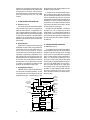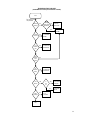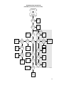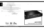
1
HT 1000™, MT 2000™,
MTS 2000™, and
MTX Series
Handie-Talkie® Portable Radios
Theory/Troubleshooting
Manual
HT 1000TM, MT 2000TM,
MTS 2000TM, and MTX Series
Handie-Talkie® Portable Radios
Theory/Troubleshooting Manual
*6881200C15*
68P81200C15-O
Motorola
8000 West Sunrise Boulevard
Fort Lauderdale, Florida 33322
Foreword
The information contained in this manual relates to all HT 1000™, MT 2000™, MTS 2000™, and MTX Series
Handie-Talkie® portable radios, unless otherwise specified.
For details on the operation of the radio, refer to the applicable manuals, which are available separately.
A list of related publications is provided in the section, “Related Publications Available Separately” on page iii.
Product Safety and RF Exposure Compliance
!
Caution
Before using this product, read the operating instructions
for safe usage contained in the Product Safety and RF
Exposure booklet enclosed with your radio.
ATTENTION!
This radio is restricted to occupational use only to satisfy FCC RF energy exposure requirements.
Before using this product, read the RF energy awareness information and operating instructions in the
Product Safety and RF Exposure booklet enclosed with your radio (Motorola Publication part number
6881095C98) to ensure compliance with RF energy exposure limits.
For a list of Motorola-approved antennas, batteries, and other accessories, visit the following web site
which lists approved accessories: <http://www.motorola.com/cgiss/index.shtml>
Manual Revisions
Changes which occur after this manual is printed are described in FMRs (Florida Manual Revisions). These FMRs provide
complete replacement pages for all added, changed, and deleted items, including pertinent parts list data, schematics, and
component layout diagrams. To obtain FMRs, contact the Radio Parts Services Division.
Computer Software Copyrights
The Motorola products described in this manual may include copyrighted Motorola computer programs stored in
semiconductor memories or other media. Laws in the United States and other countries preserve for Motorola certain
exclusive rights for copyrighted computer programs, including, but not limited to, the exclusive right to copy or reproduce in
any form the copyrighted computer program. Accordingly, any copyrighted Motorola computer programs contained in the
Motorola products described in this manual may not be copied, reproduced, modified, reverse-engineered, or distributed in
any manner without the express written permission of Motorola. Furthermore, the purchase of Motorola products shall not
be deemed to grant either directly or by implication, estoppel, or otherwise, any license under the copyrights, patents or
patent applications of Motorola, except for the normal non-exclusive license to use that arises by operation of law in the
sale of a product.
Document Copyrights
No duplication or distribution of this document or any portion thereof shall take place without the express written permission
of Motorola. No part of this manual may be reproduced, distributed, or transmitted in any form or by any means, electronic
or mechanical, for any purpose without the express written permission of Motorola.
Disclaimer
The information in this document is carefully examined, and is believed to be entirely reliable. However, no responsibility is
assumed for inaccuracies. Furthermore, Motorola reserves the right to make changes to any products herein to improve
readability, function, or design. Motorola does not assume any liability arising out of the applications or use of any product
or circuit described herein; nor does it cover any license under its patent rights nor the rights of others.
Trademarks
MOTOROLA and the Stylized M logo are registered in the US Patent & Trademark Office. All other product or service
names are the property of their respective owners.
© Motorola, Inc. 2003.
HT 1000TM, MT 2000TM,
MTS 2000TM, and MTX Series
Handie-Talkie® Portable Radios
CONTENTS
TITLE
PAGE
LIST OF TABLES...................................................................................................................................................iii
LIST OF FIGURES.................................................................................................................................................iii
RELATED PUBLICATIONS AVAILABLE SEPARATELY ......................................................................................iii
GLOSSARY OF TERMS........................................................................................................................................iv
INTRODUCTION
I. PURPOSE .......................................................................................................................................................1
II. DESCRIPTION ................................................................................................................................................1
A. General......................................................................................................................................................1
B. Printed Circuit Boards and Flexible Circuits ..............................................................................................1
THEORY OF OPERATION (BASIC FUNCTIONAL DESCRIPTION)
I. INTRODUCTION .............................................................................................................................................2
II. RADIO POWER ...............................................................................................................................................2
A. General......................................................................................................................................................2
B. B+ Routing and DC Voltage Distribution (for a Closed Architecture Controller and a
VHF or UHF Transceiver) ...................................................................................................................2
C. B+ Routing and DC Voltage Distribution (for an Open Architecture Controller and an
800 or 900MHz Transceiver)...............................................................................................................2
III. VHF/UHF TRANSCEIVER BOARD .................................................................................................................4
A. Frequency Generation Unit (See Figure 2) ...............................................................................................4
B. Antenna Switch..........................................................................................................................................4
C. Receiver Front End (See Figure 3)............................................................................................................4
D. Receiver Back End (See Figure 3) ............................................................................................................5
E. Transmitter (See Figure 4) ........................................................................................................................5
IV. 800/900MHz TRANSCEIVER BOARD ............................................................................................................6
A. Frequency Generation Unit (See Figure 5) ...............................................................................................6
B. Antenna Switch..........................................................................................................................................6
C. Receiver Front End (See Figure 6)............................................................................................................6
D. Receiver Back End (See Figure 6) ............................................................................................................7
E. Transmitter (See Figure 7) ........................................................................................................................7
V. CLOSED ARCHITECTURE CONTROLLER ...................................................................................................8
A. General (See Figure 8)..............................................................................................................................8
B. Digital Architecture ....................................................................................................................................8
C. Audio Signalling Architecture.....................................................................................................................8
VI. OPEN ARCHITECTURE CONTROLLER ........................................................................................................8
A. General (See Figure 9) ................................................................................................................................8
B. Digital Architecture ....................................................................................................................................9
C. Audio Signalling Architecture.....................................................................................................................9
, Motorola, Handie-Talkie, HT 1000, MT 2000, MTS 2000, MTX 838, MTX 8000, MTX 9000, Private-Line, Digital Private-Line,
and Privacy Plus are trademarks of Motorola, Inc.
© 1993, 2003 by Motorola, Inc.
8000 W. Sunrise Blvd., Ft. Lauderdale, FL 33322
Printed in U.S.A. 7/03. All Rights Reserved.
Theory/Troubleshooting Manual
6881200C15-A
CONTENTS (cont.)
TITLE
PAGE
THEORY OF OPERATION (DETAILED FUNCTIONAL DESCRIPTION)
I. INTRODUCTION ...........................................................................................................................................10
II. RADIO POWER .............................................................................................................................................10
A. General....................................................................................................................................................10
B. B+ Routing and DC Voltage Distribution (for a Closed Architecture Controller
and a VHF or UHF Transceiver) .......................................................................................................10
C. B+ Routing and DC Voltage Distribution (for an Open Architecture Controller
and an 800 or 900MHz Transceiver).................................................................................................11
III. VHF/UHF TRANSCEIVER .............................................................................................................................12
A. Frequency Generation Unit (FGU) ..........................................................................................................12
B. Antenna Switch........................................................................................................................................13
C. Receiver Front End..................................................................................................................................13
D. Receiver Back End ..................................................................................................................................14
E. Transmitter ..............................................................................................................................................14
IV. 800/900MHz TRANSCEIVER BOARD ..........................................................................................................15
A. Frequency Synthesis ...............................................................................................................................15
B. Antenna Switch........................................................................................................................................16
C. Receiver Front End..................................................................................................................................16
D. Receiver Back End ..................................................................................................................................17
E. Transmitter ..............................................................................................................................................17
V. CLOSED ARCHITECTURE CONTROLLER .................................................................................................17
A. Microcomputer (U705).............................................................................................................................17
B. Controller Board Circuit Operation ..........................................................................................................19
VI. OPEN ARCHITECTURE CONTROLLER ......................................................................................................21
A. Microprocessor (U705) and Associated Circuits .....................................................................................22
B. Controller Board Circuit Operation ..........................................................................................................24
VII. UNIVERSAL CONNECTOR (See Tables 2 and 3) ........................................................................................28
TROUBLESHOOTING
I. INTRODUCTION ...........................................................................................................................................30
II. TROUBLESHOOTING PROCEDURE ...........................................................................................................30
A. Check Batteries .......................................................................................................................................30
B. Alignment.................................................................................................................................................30
C. Check Overall Transmitter Operation ......................................................................................................30
D. Check Overall Receiver Operation ..........................................................................................................31
III. VOLTAGE MEASUREMENT AND SIGNAL TRACING .................................................................................31
IV. TROUBLESHOOTING CHARTS ...................................................................................................................31
(VHF/UHF Transceiver/Closed Architecture Controller) ................................................................................32
(800/900MHz Transceiver/Open Architecture Controller) ..............................................................................33
(VHF/UHF Transmitter RF) ............................................................................................................................34
(800/900MHz Transmitter RF) .......................................................................................................................35
(VHF/UHF Receiver RF) ................................................................................................................................36
(800/900MHz Receiver RF) ...........................................................................................................................37
(VHF/UHF DC Switch) ...................................................................................................................................38
(800/900MHz DC Switch) ..............................................................................................................................39
(VHF/UHF Frequency Generation Unit - FGU) ..............................................................................................40
(800/900MHz Frequency Generation Unit - FGU) .........................................................................................41
(VHF/UHF Voltage Controlled Oscillator - VCO) ...........................................................................................42
(800/900MHz Voltage Controlled Oscillator - VCO).......................................................................................43
(VHF/UHF, Closed Architecture, No Receive Audio) .....................................................................................44
(800/900MHz, Open Architecture, No Receive Audio) ..................................................................................45
(VHF/UHF, Closed Architecture, No Transmit Deviation) ..............................................................................46
(800/900MHz, Open Architecture, No Transmit Deviation)............................................................................47
(Closed Architecture Controller).....................................................................................................................48
(Open Architecture Controller) .......................................................................................................................49
(VHF/UHF Only, VCO Crossover Frequency Tune) ......................................................................................50
ii
LIST OF TABLES
TABLE
1
2
3
TITLE
PAGE
Option Select Definition...........................................................................................................18
Option Select Definition...........................................................................................................29
Universal Connector Mode......................................................................................................29
LIST OF FIGURES
FIGURE
1A
1B
2
3
4
5
6
7
8
9
TITLE
PAGE
DC Power Distribution Block Diagram
(Closed Architecture Controller and VHF or UHF Transceiver) ..........................................3
DC Power Distribution Block Diagram
(Open Architecture Controller and 800 or 900MHz Transceiver)........................................3
VHF/UHF Frequency Generation Unit (FGU) Circuits...............................................................4
VHF/UHF Receiver Block Diagram ...........................................................................................5
VHF/UHF Transmitter Block Diagram .......................................................................................5
800/900MHz Frequency Generation Unit (FGU) Circuits..........................................................6
800/900MHz Receiver Block Diagram ......................................................................................7
800/900MHz Transmitter Block Diagram ..................................................................................7
Closed Architecture Controller Block Diagram ..........................................................................8
Open Architecture Controller Block Diagram ............................................................................9
RELATED PUBLICATIONS AVAILABLE SEPARATELY
Theory Manual (this publication) ........................................................................................................68P81200C15
includes:
•
theory of operation
•
troubleshooting information and troubleshooting charts
Service Manual 68P81200C25
includes:
•
all servicing information
•
assembly / disassembly
•
maintenance
Operating Instructions
•
HT 1000 Portable Radios......................................................................................................68P81071C70
•
MT 2000 Portable Radios .....................................................................................................68P81076C65
•
MTS 2000 I Portable Radios................................................................................................68P81072C15
•
MTS 2000 II and III Portable Radios...................................................................................68P81072C45
•
MTX Series Model B3 Privacy Plus Portable Radios............................................................68P81072C10
•
MTX Series Model B4 Privacy Plus Portable Radios............................................................68P81073C60
•
MTX Series Model B5 and B7 Privacy Plus Portable Radios ...............................................68P81072C40
Mobile Vehicular Adapter (MTVA) Operating Instructions..................................................................68P81075C85
Mobile Vehicular Adapter (MTVA) Installation Instructions ................................................................68P81075C90
Remote Speaker Microphones Operating Instructions.......................................................................68P81073C40
iii
GLOSSARY OF TERMS
ALC- Automatic Level Control; a circuit in the transmit RF path that controls RF power amplifier output, provides leveling over
frequency and voltage, and protects against high VSWR
ASF IC- Audio Signalling Filter Integrated Circuit
Closed architecture- A controller configuration that utilizes a microcomputer with internal ROM, RAM, and EEPROM
DTMF- Dual Tone Multi-frequency
DPL- Digital Private-Line™
Firmware- Software or a software/hardware combination of computer programs and data, with a fixed logic configuration
stored in a read-only memory; information can not be altered or reprogrammed
FGU- Frequency Generation Unit
FLASHport™- Is a Motorola term that describes the ability of a radio to change memory. Every FLASHport radio contains a
FLASHport EEPROM memory chip that can be software written and rewritten to, again and again.
ISW- Inbound Signalling Word; data transmitted on the control channel from a subscriber unit to the central control unit
LSH- Low Speed Handshake; 150 baud digital data sent to the radio during trunked operation while receiving audio
MDC- Motorola Digital Communications
MRTI- Motorola Radio-Telephone Interconnect; a system that provides a repeater connection to the Public Switched
Telephone Network (PSTN). The MRTI allows the radio to access the telephone network when the proper access code is
received.
MSK- Minimum-Shift Keying
OMPAC- Over-Molded Pad-Array Carrier; a Motorola custom package, distinguished by the presence of solder balls on the
bottom pads
Open architecture- A controller configuration that utilizes a microprocessor with extended ROM, RAM, and EEPROM
OSW- Outbound Signalling Word; data transmitted on the control channel from the central controller to the subscriber unit
PC Board- Printed Circuit Board
PL- Private-Line® tone squelch; a continuous sub-audible tone that is transmitted along with the carrier
PLL- Phase-Locked Loop; a circuit in which an oscillator is kept in phase with a reference, usually after passing through a
frequency divider
PTT- Push-To-Talk; the switch located on the left side of the radio which, when pressed, causes the radio to transmit
Registers- Short-term data-storage circuits within the microcontroller
Repeater- Remote transmit/receive facility that re-transmits received signals in order to improve communications coverage
RESET- Reset line; an input to the microcontroller that restarts execution
RF PA- Radio Frequency Power Amplifier
RSSI- Received Signal Strength Indicator; a dc voltage proportional to the received RF signal strength
RPT/TA- Repeater/Talk-Around
RX DATA- Recovered digital data line
SCI IN- Serial Communication Interface Input line
SLIC- Support-Logic IC; a custom gate array used to provide I/O and memory expansion for the microprocessor
Softpot- Software potentiometer; a computer-adjustable electronic attenuator
Software- computer programs, procedures, rules, documentation, and data pertaining to the operation of a system
SPI (clock and data lines)- Serial Peripheral Interface; how the microcontroller communicates to modules and ICs through
the CLOCK and DATA lines
Squelch- Muting of audio circuits when received signal levels fall below a pre-determined value
SRAM- Static-RAM chip used for scratch-pad memory
Standby mode- An operating mode whereby the radio is muted but still continues to receive data
System central controller- Main control unit of the trunked dispatch system; handles ISW and OSW messages to and from
subscriber units (see ISW and OSW)
System select- The act of selecting the desired operating system with the system-select switch (also, the name given to this
switch)
TOT- Time-Out Timer; a timer that limits the length of a transmission
TSOP- Thin Small-Outline Package
µC- Microcomputer
µP- Microprocessor
VCO- Voltage-Controlled Oscillator; an oscillator whereby the frequency of oscillation can be varied by changing a control
voltage
VCOB IC- Voltage-Controlled Oscillator Buffer Integrated Circuit
VSWR- Voltage Standing Wave Ratio
iv
INTRODUCTION
I.
PURPOSE
This manual will provide a theoretical explanation of
the HT 1000, MT 2000, MTS 2000, and MTX Series
portable radio’s operation, troubleshooting, and additional useful information about the radio not found in
any other publication. The manual is divided into three
sections:
•
•
•
INTRODUCTION
THEORY OF OPERATION
TROUBLESHOOTING
In the THEORY OF OPERATION section, a basic
functional description is followed with a more detailed
description of some selected circuits. All applicable frequency bands are covered in this publication.
A complete list of models and each model’s description is provided in a separate service manual. A detailed
description of the radio’s operational features, a list of
applicable batteries and accessories, and a section on
general radio information is provided in several operating instruction manuals. To help you with your selection,
a complete list of the other publications on HT 1000, MT
2000, MTS 2000, and MTX Series portable radios can
be found following the Table of Contents of this manual.
II. DESCRIPTION
A. General
The HT 1000 Handie-Talkie portable radio is a
microcomputer-based, single-mode (conventional)
transceiver. The MT 2000, MTS 2000, and MTX Series
Handie-Talkie portable radios are microprocessor-based
dual-mode (trunked/conventional) transceivers. In all of
the radios, the microcomputer determines the active
state of the radio (transmit/receive), monitors radio status, and processes operator commands entered from
the keypad (if applicable) or the other radio controls.
Various switches, buttons, knobs, and indicators are
ergonomically designed, making placement in strategic
locations on the different model radios. Refer to the specific operating instructions on your radio for location and
description of these controls. All of the controls, including the push-to-talk (PTT) switch and key pad
(if applicable) are weather resistant. The microphone
and speaker are covered by a diaphragm for additional
protection.
B. Printed Circuit Boards and Flexible Circuits
Most of the radio circuitry is contained in chip carriers that are mounted on one of the two rigid, printed
circuit boards (PC boards); the controller board and the
transceiver board. Front display model radios contain a
third rigid PC Board; the keypad/display board, which is
a two-sided board supporting the DTMF keypad, and a
14-character, dot-matrix display. This board is not field
serviceable. If a fault develops with the keypad, display,
or backlights, the entire board must be replaced. Also,
the top-display model radios contain a small display
board located under the top escutcheon. This provides
2-character, 6-segment, starburst-type display. This
board is not field serviceable. The entire board must be
replaced.
All discrete wiring has been replaced with flexible
circuits: a controls flex, a front cover/display flex, and a
jumper flex. The controls flex interconnects the top controls and the side controls (PTT switch, emergency push
button, telephone-interconnect push button) with the
controller board. The front cover/display flex routes signals between the controller, the 13-pin universal
connector, the front cover components (speaker and
microphone), and if applicable, the display/keypad
board. The jumper flex routes signals between the
transceiver and the controller board.
1
THEORY OF OPERATION (BASIC FUNCTIONAL DESCRIPTION)
I.
INTRODUCTION
This publication covers a large family of portable
radios: HT 1000, MT 2000, MTS 2000, and MTX series
units. They are software driven, and because of the
wide range of operating systems and radio functionality
provided by this family of radios, the theory discussions
will be divided into several major categories. The
transceiver is frequency sensitive and falls into one of
four frequency bands: vhf, uhf, 800MHz, or 900MHz.
Because of their similarity, transceivers will be categorized into two discussion groups: vhf/uhf transceivers
and 800/900MHz transceivers. The controller falls into
two categories: a closed architecture controller and an
open architecture controller. Each controller will be discussed separately. This THEORY OF OPERATION
section of the manual provides a functional description
of the radio. First, overall radio functions are discussed
in basic terms, with each circuit and its relationship to
other parts of the radio described. Then, a more detailed
functional description is given for circuit relationships,
with special attention directed to some of the selected
circuits. Pay particular attention to the topics being discussed, and note the application: vhf/uhf transceiver,
open architecture controller, etc.
II. RADIO POWER
A. General
In this family of radios, power is distributed to four
general combinations of transmitters and controllers:
1.
2.
3.
4.
vhf/uhf xcvr with closed architecture controller
vhf/uhf xcvr with open architecture controller
800/900MHz xcvr with closed architecture controller
800/900MHz xcvr with open architecture controller
Discussing each of the four combinations would be
somewhat redundant, so pairs 1 and 4 were chosen for
illustration and explanation in the following paragraphs.
Paragraph B covers the vhf/uhf transceiver and the
closed architecture controller; paragraph C covers the
800/900MHz transceiver and the open architecture controller.
B. B+ Routing and DC Voltage Distribution
(for a Closed Architecture Controller and a
VHF or UHF Transceiver)
Operating power for the radio is derived from a 7.5volt battery (BATT 7.5V), which is applied directly to the
transceiver board as B+. The B+ voltage is fused and
routed through the jumper flex as Raw B+ and applied
through the controller board to the controls flex. In the
controls flex, B+ is applied to the on/off/volume control.
When the radio is turned on, switched B+ (SB+) and the
2
voltage sources required to operate various stages of
the radio are distributed as shown in Figure1A.
The power amplifier (PA) module (U105) and automatic level control (ALC) IC (U101) of the RF board are
powered-up directly from the BATT B+. Other sections
of the transceiver board are powered-up through the
switched B+. Two 5-volt regulators are used on the
transceiver board; one 5V regulator (U202) is used to
supply those circuits which require voltages to be on all
the time, such as the reference oscillator, synthesizer
IC, IF IC, and digital-to-analog (D/A) IC. The voltagecontrol oscillator (VCO) buffer obtains its voltage (Vcc)
from the SOUT line of the synthesizer. The other 5V
regulator (U103) of the transceiver board supplies 5V to
the receiver RF AMP IC and Mixer IC during the receive
mode and to the ALC and other transmitter circuitry during the transmit mode.
The controller board obtains its voltage source from
switched B+, and produces regulated 5 volts from two
regulators. One 5V regulator (U709) is used to supply
5V to the microcomputer. The SB+ is also connected to
the AUDIO PA. The audio signalling filter (ASF) IC
obtains its 5V (Vcc) from the AUDIO PA (U706) internal
5V regulator.
C. B+ Routing and DC Voltage Distribution
(for an Open Architecture Controller and an
800 or 900MHz Transceiver)
Refer to figure 1B and note that operating power for
the radio is derived from a 7.5-volt battery (BATT 7.5V),
which is applied directly to the transceiver board as B+.
The B+ voltage is fused and routed through the jumper
flex as Raw B+ and applied to the controller board.
From the controller, B+ is applied to three different
areas:
1. the expansion board, via connector jack J702 pin1,
2. an electrical switch IC, U712 pins 2 and 3, and
3. the controls flex, via connector jack J703 pin 8.
The UNSW B+ is routed to the expansion board so
that functions there can be performed independently of
the SW B+ supply. The UNSW B+ is also routed to the
electrical switch IC, U712 (a P-channel FET in an SOIC8 package), which connects it to SW B+ when the
control voltage at U712 pin 4 is low. The SW B+ is then
distributed to the rest of the radio, including the
transceiver board, front cover/display flex, and expansion board, as well as other controller board circuitry.
Finally, UNSW B+ is routed to the mechanical on/off
switch and returns to the controller as MECH SWB+.
The MECH SWB+ signal activates the electrical switch
(U712), and also feeds a resistive divider so that the
microprocessor (U705) can monitor the battery voltage.
SB+
U709
U706
5V
Regulator
Audio PA
SB+
On
5V
Off
B+
5V
U701
U705
Micro C
Controls
Flex
ASF IC
B+
Controller Board
SB+
Front Cover
Flex
Opt B+
Universal Connector
SB+
Jumper Flex
Raw B+
SB+
Fuse
1 Amp
Harmonic
Filter
U101
L105
CR109 CR108
Vcc
L122
L121
SB+
PA Module
ALC
RX
RF Amp
+
Battery
7.5V
U105
T5
5V
Regulator
VCOB IC
U201
U202
5V
T5
Mixer
Q107
R5
Q105
S
Out
R/T
5V
Ref Osc
Synth
U103
5V
Regulator
IF IC
D/A IC
Transceiver Board
Figure 1A. DC Power Distribution Block Diagram (Closed Architecture Controller and VHF or UHF Transceiver)
MECH SB+
SB+
SLIC
U709
U706
FLASH
5V
Regulator
EEPROM
U705
5V
On
Audio PA
Q702
Q703
Off
U701
Micro P
Controls
Flex
*U601
HEAR/
CLEAR
ASF IC
SB+
SRAM
U712
Electrical
Switch
Controller Board
Raw B+
B+ CNTL
Expansion
Board
* U601 HEAR/CLEAR used on 900 MHz radios only.
Front Cover
Flex
Opt B+
Universal Connector
SB+
Jumper Flex
SB+
Raw B+
RX
CR108
Fuse
1 Amp
L105
CR109
BATT B+
U101
U105
T5
VCO
PA Module
VCOB IC
5V
Regulator
Q101
+
Battery
7.5V
ALC
C138
Vss
T5
R5
5V
Q108
S
Out
R5
RF Amp
U202
Mixer
Synth
Ref Osc
IF IC
D/A IC
Transceiver Board
Figure 1B. DC Power Distribution Block Diagram (Open Architecture Controller and 800 or 900MHz Transceiver)
3
In the transceiver, SWB+ is routed directly to the 5v
regulator (U202). The regulated 5v supplies the IF IC
(U3), the reference oscillator (U203), the Fractional-N
synthesizer IC (U204), the D/A IC (U102), and the R/T
switch (Q108).
VCO buffer signal is applied to a comparator in the synthesizer. The synthesizer comparator also receives a
reference frequency via a reference divider input from
the 16.8 MHz temperature-compensated reference
oscillator. If the two frequencies differ, the synthesizer
generates a control (error) voltage which causes the
VCO to change frequency.
Internal to the synthesizer is a superfilter which supplies the VCO module (U205) and the VCO buffer IC
(U201) with 4.6 volts, produced by the regulated 5V
supply.
Modulation of the carrier is achieved by using a 2port modulation technique. The deviation of the low
frequency tone, such as DPL/TPL, is achieved by injecting the signal to an analog/digital circuit in the
synthesizer. The resultant digitized signal is then modulated by the fractional N-divider, thus generating the
required deviation. The deviation of the high frequency
tone is achieved by modulating the modulation varactor
on the VCO. In order to cover a very wide bandwidth,
the VCO control voltage is stepped up by using a positive and negative multiplier circuit. A 13-volt supply
powers the phase detector circuitry. The VCO signal is
amplified by the integrated buffer amplifier of the VCO
buffer. The two output signals, receiver first LO injection
and transmitter carrier frequency, are filtered and then
routed to the mixer/buffer (U2) and the RF PA (U105),
respectively.
In addition, two more 5-volt supplies exist, one for
transmit and one for receive: T5 and R5, respectively.
The regulated 5v is switched to either one or the other
by transistor Q108, under the control of the D/A IC. The
T5 voltage is used as a control line by the TX ALC IC
and provides bias for the RF PA input and the external
antenna connector. The R5 voltage is supplied to the
RF amplifier (U1) and the Mixer Buffer IC (U2).
III. VHF/UHF TRANSCEIVER BOARD
A. Frequency Generation Unit (See Figure 2)
The frequency generation unit (FGU) consists of
three major sections: the high stability reference oscillator(U203), fractional-N synthesizer (U204), and VCO
buffer IC(U201). The VCO provides the carrier frequency for the transmitter (TX OUT), and provides the local
oscillator (LO) injection signal for the receiver mixer
buffer (RX OUT).
B. Antenna Switch
The function of the antenna switch is to route the
transmitter power to the antenna during the transmit
mode, or route RF from the antenna to the receiver front
end during the receive mode.
The RX VCO uses an external active device, whereas the TX VCO uses the internal device of the VCO
buffer IC. The phase lock loop (PLL) circuit is provided
by the fractional-N synthesizer IC.
C. Receiver Front End (See Figure 3)
The RF signal from the antenna is coupled to the
first bandpass filter through the antenna switch. The output of the bandpass filter is then applied to a wideband
RF amplifier IC (RF AMP). The bandpass filter is electronically tuned by the D/A IC, which is controlled by the
microcomputer. Wideband operation of the filter is
achieved by retuning the bandpass filter across the
band. After amplification, the RF signal is further filtered
by a second fixed-tuned filter to improve the spurious
rejection.
The output of the VCO is amplified by the prescaler
buffer, routed through a low-pass filter, and applied to
the prescaler divider of the synthesizer. The divide ratios
are determined from information stored in memory that
was bussed to the synthesizer via the microcomputer.
The microcomputer extracts data for the division ratio as
determined by the channel select switch. The resultant
Negative Multiplier
Positive Multiplier
Switching CCTS
for VCO and Buffer
16.8 MHz
Ref Osc
Reference
Divider
Loop
Filter
Counter for
Multiplier
Fractional
Divider
A/D
U204
2.1/2.4 MHz
Reference
Clock to Modulating
ASFIC
Signal
4
Mod Out
RX VCO
TX VCO
RX Out
Low Pass
Filter
Mixer/Buffer
TX Out
Matching
CCT
RF PA Input
RX Buffer
TX Buffer
Pre-scaler
Divider
Prescaler
Buffer
Fractional-N
Synthesizer
U201
VCO Buffer IC
Low Pass Filter
Figure 2. VHF/UHF Frequency Generation Unit (FGU) Circuits
MAEPF-23266-O
The filtered RF signal is then applied to the RF input
of a broadband mixer IC. An injection signal (FIRST
LO), supplied by the FGU, is applied to the second input
of the mixer stage. The resulting difference frequency
(44.85MHz for VHF and 73.35MHz for UHF), is the first
IF frequency. The first IF frequency is then filtered by a
2-pole crystal filter to remove unwanted mixer products
and routed to the IF IC.
is replaced by internal filters in the IF IC. The IF IC uses
a type of direct conversion process where the second
LO frequency is very close to the first IF frequency. The
IF IC controls the second LO VCO and causes the VCO
to track the first IF frequency, producing a phase-locked
operation. The IF IC also provides a recovered signalstrength indicator (RSSI) and squelch output for use in
other parts of the radio.
D. Receiver Back End (See Figure 3)
E. Transmitter (See Figure 4)
In the IF IC, the first IF frequency is down converted, amplified, filtered, and demodulated to produce the
recovered audio. The IF IC is electronically programmable, and the amount of filtering, which is
dependent on the radio channel spacing, is controlled
by the microcomputer. Additional filtering, which used to
be provided externally by a conventional ceramic filter,
Antenna
RF Jack
Pin Diode
Antenna
Switch
Varactor
Tuned Filter
The transmitter consists of the following stages:
•
•
•
Harmonic Filter
RF Power Amplifier
ALC IC, which controls the power output
Harmonics of the carrier frequency are generated
by the PA module and antenna switch. The harmonic filter circuit attenuates the unwanted signals.
RF Amp
Fixed Tuned
Filter
Mixer
Crystal
Filter
AGC
SPI Bus
D/A
First LO
From FGU
Recovered Audio
Squelch
Demodulator
RSSI
I-F IC
Synthesizer
16.8 MHz
Reference Clock
SPI Bus
MAEPF-23265-O
Second
LO VCO
Figure 3. VHF/UHF Receiver Block Diagram
Batt B+
V Supply
Antenna
Pin Diode
Antenna
Switch
VCO
Synthesizer
RF PA
Harmonic
Filter
RF Jack
Coupler
To Receiver
Front End
V Det
V Control
B+
V
ALC IC
V Ref
MAEPF-23264-O
Figure 4. VHF/UHF Transmitter Block Diagram
5
The RF PA module is a multi-stage amplifier, which
has the required gain to produce an output level of several watts. Some harmonic filtering is accomplished in
the RF PA.
IV. 800/900MHz TRANSCEIVER BOARD
Modulation of the carrier is achieved by using a 2port modulation technique. The deviation of the low
frequency tone, such as DPL/TPL, is achieved by injecting the signal to an analog/digital circuit in the
synthesizer. The resultant digitized signal is then modulated by the fractional N-divider, thus generating the
required deviation. The deviation of the high frequency
tone is achieved by modulating the modulation varactor
on the VCO. In order to cover a very wide bandwidth,
the VCO control voltage is stepped up by using a positive multiplier circuit. A 13-volt supply powers the phase
detector circuitry. The VCO signal is amplified by the
integrated buffer amplifier of the VCO buffer. The two
output signals, receiver first LO injection and transmitter
carrier frequency, are filtered and then routed to the
mixer/buffer (U2) and the RF PA (U105), respectively.
A. Frequency Generation Unit (See Figure 5)
B. Antenna Switch
The frequency generation unit (FGU) consists of the
following major sections: the high stability reference
oscillator (U203), fractional-N synthesizer (U204), VCO
buffer IC (U201), and VCO (U205). The VCO provides
the carrier frequency for the transmitter (TX OUT), and
provides the local oscillator (LO) injection signal for the
receiver mixer buffer (RX OUT). The phase lock loop
(PLL) circuit is provided by the fractional-N synthesizer
IC.
The function of the antenna switch is to route the
transmitter power to the antenna during the transmit
mode, or route the RF from the antenna, to the receiver
front end during the receive mode.
Power control is achieved by using the coupler
detector to feed back a portion of the PA output to the
ALC circuit. This ALC circuit increases or decreases the
overall PA gain as appropriate. Another function of the
detector is to provide a signal when the VSWR exceeds
the threshold level. This signal, combined with the
forward detected power, is used to reduce the PA output
power, thus protecting the PA under high VSWR
conditions.
The output of the VCO is amplified by the prescaler
buffer, routed through a low-pass filter, and applied to
the prescaler dividers of the synthesizer. The divide
ratios are determined from information stored in memory
that is bussed to the synthesizer via the microprocessor.
The microprocessor extracts data for the division ratio
as determined by the channel-select switch. The resultant VCO buffer signal is applied to a comparator in the
synthesizer. The synthesizer comparator also receives a
reference frequency via a reference divider input from
the 16.8 MHz temperature-compensated reference
oscillator. If the two frequencies differ, the synthesizer
generates a control (error) voltage which causes the
VCO to change frequency.
Positive Multiplier
To
I-F IC
Loop
Filter
Counter for
Multiplier
TX VCO
6
RX Out
Low Pass
Filter
Mixer/Buffer
TX Out
Matching
CCT
RF PA Input
RX Buffer
Mod Out
Fractional
Divider
2.1/2.4 MHz
Reference
Clock to Modulating
ASFIC
Signal
The filtered RF signal is then applied to the RF input
of a broadband mixer IC, U2. An injection signal (FIRST
LO) supplied by the FGU, is applied to the second input
of the mixer stage. The resulting difference frequency of
73.35MHz is the first IF frequency. The first IF frequency
is then filtered by a 2-pole crystal filter, FL1, to remove
unwanted mixer products and routed to the IF IC, U3
RX VCO
Reference
Divider
U204
The RF signal from the antenna is coupled to the
first bandpass filter through the antenna switch. The output of the bandpass filter is then applied to a wideband
RF amplifier IC (RF AMP). The bandpass filter is a wideband stripline filter, which is pretuned for the frequency
band. After amplification, the RF signal is further filtered
by a second fixed-tuned stripline filter to improve the
spurious rejection.
Switching CCTS
for VCO and Buffer
16.8 MHz
Ref Osc
A/D
C. Receiver Front End (See Figure 6)
TX Buffer
Pre-scaler
Divider
Prescaler
Buffer
Fractional-N
Synthesizer
U201
VCO Buffer IC
Low Pass Filter
Figure 5. 800/900MHz Frequency Generation Unit (FGU) Circuits
MAEPF-23421-O
D. Receiver Back End (See Figure 6)
E. Transmitter (See Figure 7)
In the IF IC, the first IF frequency is down converted, amplified, filtered, and demodulated to produce the
recovered audio. The IF IC is electronically programmable, and the amount of filtering, which is
dependent on the radio channel spacing, is controlled
by the microprocessor. Filtering is accomplished by
internal filters in the IF IC. The IF IC uses a type of
direct conversion process where the second LO frequency is very close to the first IF frequency. The IF IC
controls the second LO VCO and causes the VCO to
track the first IF frequency, producing a phase-locked
operation. The IF IC also provides a recovered signalstrength indicator (RSSI) and squelch output for use in
other parts of the radio.
Antenna
RF Jack
Pin Diode
Antenna
Switch
Stripline
Filter
The transmitter consists of the following stages:
•
•
•
Low-pass antenna matching circuit
RF Power Amplifier
ALC IC and coupler, for power output control
The low-pass antenna matching circuit attenuates
RF PA harmonics, and provides the optimum phase
load to the RF PA. The RF PA module is a multi-stage
amplifier, which has the required gain to produce an output level of several watts. Some harmonic filtering is
also accomplished in the RF PA.
Power control is achieved by using the coupler
detector to feed back a portion of the PA output to the
ALC circuit. This ALC circuit increases or decreases the
Stripline
Filter
RF Amp
Mixer
Crystal
Filter
AGC
First LO
From FGU
Recovered Audio
Squelch
Demodulator
RSSI
Synthesizer
IF IC
16.8 MHz
Reference Clock
MAEPF-23420-O
SPI Bus
Second
LO VCO
Figure 6. 800/900MHz Receiver Block Diagram
Batt B+
V Supply
Antenna
Pin Diodes
Antenna
Switch
VCO
Synthesizer
RF PA
RF Jack
Coupler
To Receiver
Front End
V Det
V Control
B+
V Ref.
ALC IC
MAEPF-23419-O
V Ref
Figure 7. 800/900MHz Transmitter Block Diagram
7
overall PA gain as appropriate. Another function of the
detector is to provide a signal when the VSWR exceeds
the threshold level. This signal, combined with the
forward detected power, is used to reduce the PA output
power, thus protecting the PA under high VSWR
conditions.
V. CLOSED ARCHITECTURE CONTROLLER
A. General (See Figure 8)
The controller board is the central interface between
various subsystems of the radio. It is segregated into
digital and audio architecture. The digital portion consists of a special Motorola microcomputer. The audio
power amplifier (AUDIO PA) and audio/signalling/filter
IC (ASF IC) form the backbone of the audio/signalling
architecture. The controller board has its own voltage
regulators to generate 5 volts, sourced by switched B+
from the battery.
B. Digital Architecture
transmit and receive audio, and also provides PL, DPL,
and MDC encoding and decoding.
In the transmit mode, the ASF IC amplifies, shapes,
limits, and filters the outgoing signal. The processed signal is sent to the transceiver board’s FGU. In the receive
mode, the demodulated signal from the receiver back
end is amplified, filtered and routed to the AUDIO PA for
amplification. The ASF IC provides pre-emphasis and
de-emphasis as well as squelch. Based on a reference
signal from the transceiver board, the ASF IC provides
the microcomputer with a clock signal.
Received audio signal amplification is achieved by
the AUDIO PA IC. The IC’s output drives the radio’s
internal speaker, or an external speaker connected via
an option cable. In order to minimize the effects, and to
further isolate the audio signals from the digital signals,
the audio section has its own isolated 5V regulator on
the AUDIO PA.
VI. OPEN ARCHITECTURE CONTROLLER
The Motorola microcomputer consists of 640 bytes
of EEPROM, 760 bytes of RAM, and 24k of ROM. The
microcomputer executes the radio software and monitors the activity of all user interfaces. Using the
communication buses, the microcomputer handles the
responsibility of programming all applicable ICs in the
radio, including those on the RF transceiver board. This
programming sets up the ICs to properly perform a variety of functions, such as what frequency to transmit or
what channels to scan. The digital circuitry is powered
by a discrete 5-volt regulator to help isolate the digital
signals from the audio signals in nearby circuits.
C. Audio Signalling Architecture
A Motorola custom IC (ASF) provides both transmit
and receive audio and signalling processing. The ASF
IC is programmable by the microcomputer via the serial
peripheral interface (SPI). It provides filtering on both
TO FGU
2.1/2.4 MHz
Reference Clock
From FGU
Recovered Audio
Squelch
A. General (See Figure 9)
The controller board is the central interface between
various subsystems of the radio. The controller board is
composed of both digital and audio circuits. The digital
portion consists of a special Motorola microprocessor
(U705), a custom, gate-array, memory-support-logic IC
(SLIC), U710, and the memory devices (U713, U714,
and U715). The audio circuits include the audio power
amplifier (U702), the audio/signalling/filter IC (ASF IC),
U701, and in the 900MHz radios, the Hear Clear IC,
U601. The controller board has its own voltage regulators to generate 5 volts, sourced by switched B+ from
the battery. The open architecture controller board also
has a plug-in interface for secure voice encryption
options, and another interface for the display and keypad version radios.
External
Microphone
Internal
Microphone
MOD
Out
Audio/Signalling
Architecture
Audio Filter and
Signalling IC
External
Speaker
Audio
PA
Internal
Speaker
SPI
To RF Board
Digital
Architecture
uP Clock
SCI to Side
Connector
768 RAM
640 EEPROM
HC11K4
5V
Regulator
24K ROM
MAEPF-23267-O
8
Figure 8. Closed Architecture Controller Block Diagram
External
Microphone
Internal
Microphone
2.1/2.4 MHz
REF Clock
From FGU
Squelch
Expander
External
Speaker
U702
Audio
PA
Compressor
Recovered
Audio
Internal
Speaker
U701
ASF IC
Flutter
Filter
Audio/
Signalling
Architecture
*U601
HEAR/CLEAR
Mod Out
To FGU
SPI
To Receiver
Board
uP
Clock
U710
SLIC
Masked ROM
or
FLASH
U705
MCII FI
u Processor
SCI
To Universal
Connector
EEPROM
SRAM
Digital
Architecture
MAEPF-23422-O
* U601 HEAR/CLEAR used on 900 MHz radios only.
Figure 9. Open Architecture Controller Block Diagram
B. Digital Architecture
C. Audio Signalling Architecture
The Motorola microprocessor, in conjunction with
the SLIC, performs the functions of controlling the internal workings of the radio, as well as interfacing with the
outside world. The microprocessor has 1K of RAM and
512 bytes of EEPROM on the chip. In some versions
the controller board enhances the capabilities of the
microprocessor chip by providing 256K or 512K of
FLASH memory, 32K static RAM, and 8K or 32K of
EEPROM. Other versions use masked programmed
ROM.
The Motorola custom integrated circuit, ASF IC, performs audio signal shaping and filtering. The ASF IC
also encodes and decodes Private-Line (PL), Digital Private-Line (DPL), and Motorola Digital Communication
(MDC) signals, as well as decoding trunking signals.
The “FLASH” open controller is flexible and capable
of firmware being reprogrammed to support future features. The controller, through communication busses,
programs all applicable ICs in the radio (including those
on the transceiver board) for proper operation in the
designated frequency band.
In the transmit mode, the ASF IC amplifies and
shapes the modulating signal on its way to the modulating port of the FGU. In the receive mode, the ASF IC
amplifies and filters the demodulated signal and applies
it to the audio PA, which drives the internal or external
radio speaker. The ASF IC not only performs preemphasis and de-emphasis, but also performs the
squelch functions and provides the microprocessor with
a clock signal.
9
THEORY OF OPERATION (DETAILED FUNCTIONAL DESCRIPTION)
I.
INTRODUCTION
In this section of the of the manual, a more detailed
description of the radio and some special circuit is given.
For a better understanding of the circuits descriptions,
and to aid in following the text, refer to the applicable
schematic diagram(s) in the corresponding service manual (Motorola part number 68P81200C25), or previously
68P81200C20.
II. RADIO POWER
A. General
As previously described in the THEORY OF OPERATION (BASIC FUNCTIONAL DESCRIPTION) RADIO
POWER paragraph, power is distributed to four general
combinations of transmitters and controllers:
1. VHF/UHF transceiver with closed architecture
controller,
2. VHF/UHF transceiver with open architecture
controller,
3. 800/900MHz transceiver with closed architecture
controller, and
4. 800/900MHz transceiver with open architecture
controller
Discussing each of the four combinations would be
somewhat redundant, so pairs 1 and 4 were chosen for
explanation in the following paragraphs. Paragraph B
covers the vhf/uhf transceiver and the closed architecture controller; paragraph C covers the 800/900MHz
transceiver and the open architecture controller.
B. B+ Routing and DC Voltage Distribution
(for a Closed Architecture Controller and a
VHF or UHF Transceiver)
Raw B+ (7.5V) from the battery (Batt B+) enters the
radio on the transceiver board through a 3-contact
spring pin arrangement (P404) as B+, where it is routed
directly to the RF PA Module and ALC IC pin 13. Battery
B+ is fused, and then routed through the jumper flex
(P704, pins1 and 20) to the controller board (J704, pins
1 and 20). The B+ supply is routed through the controller board to the on/off/volume control (S403/ R401)
on the controls flex at jack J703, pin 8. With the
mechanical on/off switch (S403) placed in the on position, switched B+ (SB+) is routed from the controls flex
at connector plug P703, pin 10 and applied to the controller at connector jack J703, pin10. This signal is also
fed to a resistive divider R708, R709 so that the microcomputer (U705) can monitor the battery voltage.
The SB+ voltage powers the audio PA (U706) and
its internal 5V regulator booster transistor (Q702). It also
powers a discrete 5V regulator (U709). Regulated 5
volts from module U709 powers the microcomputer
10
(U705) and other digital circuitry. The ASF IC (U701)
obtains its 5V (Vcc) from the AUDIO PA internal 5V regulator through a booster transistor (Q702)
The switched B+ voltage supplies power to circuits
on the transceiver board. The 5-volt regulator, U202, is
applied this voltage through decoupling component
C125 to produce a stable 5.0 volt output. Raw B+ (7.5V)
which is connected to the ALC IC (U101), is switched
through the output (CATH1) to another 5-volt regulator
(U103).
Regulator U202 supplies those circuits which need
to remain on at all times, such as the reference oscillator
(U203), fractional-N-synthesizer (U204), D/A IC (U102),
and the IF module (U3). The D/A IC controls dc switching of the transceiver board. The SC1 signal at U102 pin
12 controls transistors Q107, Q104, and the transmit
5 volts (T5). The SC3 signal at U102 pin 14 controls
transistor Q105, and the receive 5 volts (R5). A voltage
on the synthesizer SOUT line at U204 pin 19 supplies
power (Vcc) to the VCO buffer at U201 pin 3.
During the receive mode, via switching transistor
Q105, regulator U103 supplies regulated 5V (R5) to the
receiver front end. In the battery-saver mode, R5 can be
switched on and off by controlling pin 1 of transistor
Q105. Module U103 is not used during the transmit
mode. During the transmit mode, transmit 5 volts (T5)
for the ALC IC and other TX circuitry is obtained from
U202 via switching transistor Q104.
1. Low-Battery Detect Circuit (Controller Board )
The low-battery detect circuit generates an audio
alert when the radio’s battery needs recharging. The
implementation of this function takes advantage of
the microcomputer’s on-chip, 8-bit, 8-channel, A/D
converter, U705 pins PE0-PE7. The 7.5V (SB+) is
divided down to a nominal 3.92V by resistors R708
and R709, and fed to port PE4 of U705. This voltage is converted by the A/D converter to a digital
format. The microcomputer compares this voltage to
a preset low-battery trip threshold, which corresponds to a battery voltage of ~
= 7.0V in standby
or ~
= 6.2V in transmit. If the measured voltage is
lower than either threshold, the low battery alert
tone is generated (if option is enabled) to warn the
user that approximately 20 minutes of usable battery capacity remains.
2. Power for External Accessories
Via current limiting resistor R733 and associated
isolation and protection components VR715,
VR720, and C709, SB+ is available on the controller
board at connector jack J701 pin 16. From the controller board, SB+ is routed through the front-cover
flex (P701 pin 16 to J403 pin 4) and applied to to
the universal connector at P403 pin 4 as OPT B+.
The OPT B+ voltage powers external accessories
used with the radio.
C. B+ Routing and DC Voltage Distribution
(for an Open Architecture Controller and an
800 or 900MHz Transceiver)
This radio differs from previous Motorola portable
radios in that B+ from the battery is electrically switched
to most of the radio, rather than routed through the
on/off/volume switch, S403/R401. The electrical switching of B+ supports a ”keep-alive” mode. Under software
control, even when the on/off switch has been turned to
the off position, power remains on.
Raw B+ (7.5V) from the battery (Batt B+) enters the
radio on the transceiver board through a 3-contact
spring pin arrangement (P404) as B+, where it is routed
through two ferrite beads (E102 and E101) and applied
to the RF PA and the ALC IC on pin 13. Battery B+ is
fused, and is then routed to the controller board, where
it enters on connecter J704 pins 1 and 20. From the
controller, BATT B+ fans out to three different areas: (1)
the secure or data option board via connector jack J702
pin 1, (2) the electrical switch IC, U712 pins 2 and 3,
and (3) the control-top flex via connector jack J703 pin
8. UNSW B+ is routed to the secure board so that it can
perform key management and other functions independently of SW B+. UNSW B+ is routed to the electrical
switch IC, U712 (a P-channel FET in an SOIC-8 package), which connects it to SW B+ when the control
voltage at U712 pin 4 is low. SW B+ is then distributed
to the rest of the radio, including the transceiver board,
the display/keypad board, and the secure or data option
board, as well as other controller board circuitry. Finally,
UNSW B+ is routed to the mechanical ON/OFF switch
via connector jack J703 pin 8, and returns to the controller as MECH SWB+ (J703 pin 10). This signal is
used to activate the electrical switch (U712), and also is
fed to a resistive divider so that the microprocessor
(U705) can monitor the battery voltage.
The electrical switch (U712) is activated by transistor Q703, which in turn is driven by either the MECH
SWB+ or the B+ CNTL signals turning on one or both of
the diodes in CR704. Let us consider what happens
when the radio is initially off and all circuits are powered
down. When the user switches the ON/OFF switch to
the ON position, the MECH SWB+ signal will be connected to UNSW B+ and transistor Q702 will then be
turned on. Transistor Q703 pin 3 will go low (< .3 V),
and this will turn on U712, which in turn connects
UNSW B+ to SW B+. The SW B+ will then be fed to all
the other radio circuitry, and the radio will begin its normal power-on sequence. In particular, the
microprocessor, U705, will initialize after regulated Vdd
from U708 reaches 5.0 V. It can then program the gate
array (U710) so that the B+ CNTL signal can be an output high or low (initially this pin, U710-G8, is configured
as an input so that it does not drive diode CR704).
Recalling that SW B+ to the radio is controlled by
U712, which is activated by the B+ CNTL signal or
MECH SWB+ via CR704 and Q702, if the user turns off
the ON/OFF switch then MECH SWB+ drops to zero
volts. If the microprocessor has set B+ CNTL to logic
zero, then Q702’s inverted output (pin 3) will be high,
and the power switch (U712) will turn off, and SW B+
will drop to zero. If, however, the controller is programmed to support power-down de-affiliation (typically
for a trunked system only), then it will have left B+ CNTL
at a logic high. In this case, when the ON/OFF switch is
turned off, SW B+ will continue to be supplied to the
radio, but the microprocessor will sense that the switch
has turned off by reading that the voltage on pin U705PE1 has fallen to zero. The microprocessor can then
key up the transmitter and send a de-affiliation ISW to
the trunking system. After receiving and verifying an
acknowledgement, the microprocessor then shuts down
SW B+ (and therefore, its own power, since Vdd comes
from SW B+ via U708) by setting B+ CNTL=0. In summary, we see that turning the ON/OFF switch ON
always supplies power to the radio circuitry, but the
radio can only power down when the switch is OFF and
the microprocessor has set B+ CNTL=0.
1. Low-Battery/ Detect Circuit (Controller Board)
The low-battery detect circuit is used to warn the
user that the radio’s battery needs recharging.
The implementation of this function on open architecture radios takes advantage of the microprocessor’s on-chip 8-bit, 8-channel A/D converter
(pins PE0-PE7 of U705). The mechanically
switched 7.5V (MECH SWB+) is divided down to a
nominal 3.92 V by resistors R725 and R726 and
fed to port PE1 of U705. This voltage is converted
by the A/D to digital format. The microprocessor
compares this voltage to a preset low-battery trip
threshold, which corresponds to a battery voltage
of ~
= 7.0V in standby mode or ~
= 6.20V in transmit
mode. If the measured digitized voltage is lower
than either low battery threshold, the low battery
alert tone or flashing icon is generated to warn the
user that only about 20 minutes of usable battery
capacity remains.
2. Power To/From External Accessories
The switched 7.5V also powers external accessories used with the radio. The voltage is picked up
from the controller board and passed to the front
cover/display flex via connector jack J701 pin 16
(OPT B+/BOOT SEL). The front cover/display flex
then applies the voltage to pin 4 of the universal
connector, where it is picked up by external accessories. Resistor R714, with a 1W power rating,
provides current limiting to the external circuit to
prevent internal damage should the external connector short.
11
The open architecture controller board uses Flash
memory (U715) in place of conventional EPROMs.
This allows the firmware to be reprogrammed
through the side connector without opening the
radio. The smart RIB box (SRIB) is used in conjunction with the RSS software program to perform
the Flash reprogramming operation. While this
occurs, the SRIB applies 12.7 V at different times
to two of the radio side connector pins, 4 and 10.
Pin 4 is the OPT B+/BOOT SEL pin. When 12.7
volts is applied to this pin, zener diode VR713
starts conducting and turns on both transistors contained in U703. The outputs of these transistors pull
the MODA/MODB pins of U705 low and also control mux logic involving U709 to separate the
microprocessor’s SCI TX and RX paths, which are
necessary for bootstrapping code into the µC during Flash reprogramming. Diode CR701 is needed
to prevent current from flowing from the external
12.7 V source into the battery.
When 12.7 V is applied to pin 10 of the side connector, current flows through diode CR705 and
approximately 12.0 V is presented to the Vpp pin of
Flash memory (U715), which is required for reprogramming. Resistor R723 and zener diode VR715
prevent excess voltage from appearing at the input
to U710-B6 when the 12.7 volts is applied.
3. Controller Board 5V Regulators
To reduce the possibility of digital noise coupling
into the audio circuitry, the controller board uses
separate analog and digital 5V supplies. The controller board regulated 5V for the digital circuitry
(Vdd) is derived from a dedicated linear regulator
IC (U708) which also provides a low voltage reset
function. This device uses SW B+ as input and produces an output that is regulated to 5V ±0.1V. The
low voltage error output (U708 pin 5) is used to
hold the microprocessor (U705) RESET line low
during power turn-on and turn-off conditions or
when the battery is accidentally discharged to a
very low voltage; this prevents the microprocessor
from operating erratically during low voltage conditions.
The regulated analog 5V supply (Vaud) from audio
PA U702 provides the operating voltage for audio
IC U701. It is generated in conjunction with the
external PNP pass transistor Q701. The circuit
uses a negative feedback loop with an internal differential amplifier and a reference voltage inside
U702. As the load on the 5V changes, the amplified
error voltage is fed back to the base of transistor
Q701 to keep the 5V regulated to a tolerance of
±0.25V.
III. VHF/UHF TRANSCEIVER
A. Frequency Generation Unit (FGU)
The frequency generation unit (FGU) consists of
three major sections; the high stability reference oscillator (U203), the fractional-N synthesizer (U204,) and the
VCO buffer (U201). A 5V regulator (U202), supplies
power to the FGU. The synthesizer receives the 5V
REG at U204, and applies it to a filtering circuit within
the module and capacitor C253. The well filtered 5-volt
output at U204 pin 19 is distributed to the TX and RX
VCOs and the VCO buffer IC. The mixer LO injection
signal and transmit frequency are generated by the RX
VCO and TX VCO respectively. The RX VCO uses an
external active device (Q202), whereas the TX VCO
active device is a transistor inside the VCO buffer. The
base and emitter connections of this internal transistor
are pins 11 and 12 of U201.
The RX VCO is a Colpitts-type oscillator, with
capacitors C235 and C236 providing feedback. The RX
VCO transistor (Q202) is turned on when pin 38 of U204
switches from high to low. The RX VCO signal is
received by the VCO buffer at U201 pin 9, where it is
amplified by a buffer inside the IC. The amplified signal
at pin 2 is routed through a low-pass filter (L201 and
assocated capacitors) and injected as the first LO signal
into the mixer (U2 pin 8). In the VCO buffer, the RX
VCO signal (or the TX VCO signal during transmit) is
also routed to an internal prescaler buffer. The buffered
output at U201 pin 16 is applied to a low-pass filter
(L205 and associated capacitors). After filtering, the signal is routed to a prescaler divider in the synthesizer at
U204 pin 21.
The divide ratios for the prescaler circuits are determined from information stored in a codeplug, which is
part of the microprocessor (U705). The microprocessor
extracts data for the division ratio as determined by the
position of the channel-select switch (S401), and busses
the signal to a comparator in the synthesizer. A
16.8MHz reference oscillator, U203, applies the
16.8MHz signal to the synthesizer at U204 pin 14. The
oscillator signal is divided into one of three pre-determined frequencies. A time-based algorithm is used to
generate the fractional-N ratio.
If the two frequencies in the synthesizer’s comparator differ, a control (error) voltage is produced. The
phase detector error voltage (V control) at pin 31 and 33
of U204, is applied to the loop filter consisting of resistors R211, R212, and R213, and capacitors C244,
C246, C247 and C275 . The filtered voltage alters the
VCO frequency until the correct frequency is synthesized. The phase detector gain is set by components
connected to U204 pins 28 and 29.
In the TX mode, U204 pin 38 goes high and U201
pin 14 goes low, which turns off transistor Q202 and
turns on the internal TX VCO transistor in U204. The TX
VCO feedback capacitors are C219 and C220. Varactor
12
C80, C86, C87, C88, C97, C99, L3, L4, L5, and L30
(VHF); or C4 thru C7, C88 thru C94, C99, and L11 thru
L15 (UHF) to improve the spurious rejection.
Via a broadband 50-ohm transformer, T1, the filtered RF signal is routed to the input of a broadband
mixer/buffer (U2). Mixer U2 uses GaAs FETs, in a double-balanced Gilbert Cell configuration. The RF signal is
applied to the mixer at U2 pins 1 and 15. An injection
signal (1st LO) of about -10dBm, supplied by the FGU,
is applied to U2 pin 8. Mixing of the RF and the 1st LO
results in an output signal which is the first IF frequency.
The first IF frequency of VHF and UHF bands are 44.85
MHz and 73.35 MHz respectively. The 1st LO signal for
VHF is 44.85 MHz higher than the carrier frequency
while that for the UHF is 73.35 MHz lower than the carrier frequency. The 1st IF signal output, at U2 pins 4 and
6, is routed through transformer T2 and impedance
matching components, and applied to a 2-pole crystal filter (FL1), which is the final stage of the receiver front
end. The 2-pole crystal filter removes unwanted mixer
products as the filtered IF signals being routed to the IF
module, U3. Impedance matching between the output of
the transformer (T2) and the input of the filter (FL1) is
accomplished by capacitors C35 and C36 and inductor
L20.
D. Receiver Back End
The output of crystal filter FL1 is matched to the
input of IF buffer amplifier transistor Q4 by components
C39, L22 and C38. Transistor Q4 is biased by the voltage level on U2 pin 3. The IF frequency on the collector
of Q4 is applied to U3 pin 2, where it is down converted,
amplified, filtered, and demodulated, to produce the
recovered audio at U3 pin 28. This IF IC is electronically
programmable, and the amount of filtering (which is
dependent on the radio channel spacing) is controlled
by the microcomputer. Additional filtering, which used to
be provided externally by conventional ceramic filters, is
replaced by internal filters in the IF module. The IF IC
uses a type of direct conversion process where the second LO frequency is very close to the first IF frequency.
The IF IC synthesizes the second LO and phase locks
the VCO to track the first IF frequency.
In the absence of an IF signal, the VCO will “hunt,”
or its frequency will vary about a frequency close to the
IF frequency. When an IF signal is received, the VCO
will lock onto the IF signal. The 2nd LO/VCO is a Colpitts oscillator built around transistor Q1. The VCO has a
varactor diode, CR5, to adjust the VCO frequency. The
control signal for the varactor is derived from a loop filter
consisting of C52, C53, and R16.
The IF IC (U3) performs several other functions. It
provides a received signal strength indicator (RSSI) and
a squelch output. The RSSI is a dc voltage monitored by
the microcomputer and used as a peak indicator during
bench tuning of the receiver front-end varactor filter. The
RSSI dc voltage is sent from U3 pin 9 to connector jack
14
J301 pin 11, where it is routed through the jumper flex
(P301 pin 11 to P704 pin 11) and applied to the controller board. In the controller board the RSSI is routed
through the ASF IC (U701 pin 11 to U701 pin 41), and
applied to the front cover flex at J701 pin 21.Via the
front cover flex, the RSSI voltage reaches its destination, at the universal connector at P403 pin 7 as RTS.
The squelch output of U3, on pin 29, is a high-frequency
audio signal. The squelch signal is routed to shaping
and detection circuits within U701 on the controller
board, for use in other parts of the radio. The IF module
(U3) also monitors the strength of the received signal, to
provide an AGC voltage at pin 4, which is then fed to the
RF amplifier AGC circuit. Inductor L23 and capacitor
C70 prevent any IF signal from leaking back to the frontend circuits.
E. Transmitter
The transmitter consists of three major sections:
•
•
•
Harmonic Filter
RF Power Amplifier Module
ALC Circuits
1. Harmonic Filter
RF from the Power Amplifier (PA) module, U105 is
routed through the coupler (U104), passed through
the transmit antenna switch (CR108), and applied to
a harmonic filtering network. The harmonic filtering
circuit is comprised of the following components:
L126, L127, L128, C149, C150, and C151 (for VHF
models); or L126, L127, L128, C129, C130 C149,
C150, and C151 (for UHF models). Resistor R128
(UHF) or R117 (VHF) provides a current limited 5V
to P402 for mobile vehicular adapter (MTVA) applications.
2. RF Power Amplifier Module
The RF power amplifier module (U105) is a wideband multi-stage amplifier (3 stages for the VHF
models and 4 stages for the UHF models). Nominal
input and output impedance of U105 is 50 ohms.
The dc bias for U105 is on pins 2, 4, 5. In the transmit mode, the voltage on U105 pins 2 and 4 (close
to the B+ level) is obtained via switching transistor
Q101. Transistor Q101 receives its control base signal as follows:
•
•
•
the microcomputer keys the D/A IC to produce
a ready signal at U102 pin 3
the ready signal at U102 pin 3 is applied to the
TX ALC IC at U101 pin 14 (5V)
the synthesizer sends a LOC signal to the TX
ALC IC (U204 pin 40 to U101 pin 16
When the LOC signal and the ready signal are both
received, the TX ALC IC (pin 13) sends a control
signal to turn on transistor Q101.
3. ALC Circuits
Coupler module U104 samples the forward power
and the reverse power of the PA output voltage.
Reverse power is present when there is other than
50 ohms impedance at the antenna port. Sampling
is achieved by coupling some of the forward and/or
reverse power, and apply it to CR102(VHF) or
CR101(UHF) and CR103 for rectification and summing. The resultant dc signal is then applied to the
TX ALC IC (U101 pin 2) as RFDET to be used as
an RF strength indicator.
The transmit ALC circuit, built around U101, is the
heart of the power control loop. Circuits in the TX
ALC module compare the signals at U101 pins 2
and 7. The resultant signal, C BIAS, at U101 pin 4 is
applied to the base of transistor Q110. In response
to the base drive, transistor Q110 varies the dc control voltages applied to the RF PA at U105 pin 3,
thus controlling the RF power of module, U105.
Thermistor RT101 senses the temperature of the
TX ALC IC. If an abnormal operating condition
exists, which causes the PA slab temperature to
rise to an unacceptable level, the thermistor forces
the ALC to reduce the set power.
The 900MHz VCO is also a dual-range oscillator
that covers the 896-902MHz and the 935-941MHz frequency bands. The low-band VCO (861-902MHz)
provides the first LO injection frequencies (861867MHz) that will be 73.35MHz below the carrier
frequency. In addition, when the radio is operated
through a repeater, the low-band VCO will generate the
transmit frequencies (896-902MHz) that will be 39MHz
below the receiver frequencies. When talk-around operation is necessary the high-band VCO (935-941MHz) is
selected.
The buffer IC, U201, includes a TX, RX, and
prescaler buffer whose main purpose is to individually
maintain a constant output and provide isolation. The
TX buffer is chosen by setting pin 7 of U201 high; the
RX buffer is chosen by setting pin 7 of U201 low. The
prescaler buffer will always be on. In order to select the
proper combination of VCO and buffer, the following
conditions must be true at pin 6 of U201 (or pin 38 of
U204) and pin 7 of U201 (or pin 39 of U204). For the
first LO injection frequencies 861-867MHz (A), pins 6
and 7 must both be low; for the TX repeater frequencies
896-902 MHz (B) pins 6 and 7 must both be high, and
for talk-around TX frequencies 935-941 MHz (C) pin 6
must be low while pin 7 must be high.
(A) =
IV. 800/900MHz TRANSCEIVER BOARD
(B) =
A. Frequency Synthesis
The complete synthesizer subsystem consists of the
reference oscillator (U203), the voltage controlled
oscillator (VCO), U205, a buffer IC (U201), and the
synthesizer U204).
The reference oscillator contains a temperaturecompensated 16.8 MHz crystal. This oscillator is digitally
tuned and contains a temperature-referenced 5-bit analog-to-digital (A/D) converter. The output of the oscillator
(pin 10 on U203) is applied to pin 14 (XTAL1) on U204
via capacitor C284 and resistor R222.
Module U205 is the voltage controlled oscillator,
which is varactor tuned; that is, as the voltage (2-11V)
being applied to pins 1 and 7 of the VCO varies, so
does the varactor’s capacitance, thereby changing the
VCO’s output frequency. The 800MHz VCO is a dualrange oscillator that covers the 806-825MHz and the
851-870MHz frequency bands. The low-band VCO
(777-825MHz) provides the first LO injection frequencies (777-797MHz) that will be 73.35MHz below the
carrier frequency. In addition, when the radio is operated
through a repeater, the low band VCO will generate the
transmit frequencies (806-825MHz) that will be 45MHz
below the receiver frequencies. The low-band VCO is
selected by pulling pin 3 high and pin 8 low on U205.
When radio-to-radio or talk-around operation is necessary, the high band VCO (851-870MHz) is selected.
This is accomplished by pulling pin 3 low and pin 8 high
on U205.
(C) =
777-797MHz for 800MHz; 861-867MHz
for 900MHz
804-825MHz for 800MHz; 896-902MHz
for 900MHz
851-870MHz for 800MHz;935-941MHz
for 900MHz
The synthesizer IC, U201 consists of a prescaler, a
programmable loop divider, a divider control logic, a
phase detector, a charge pump, an A/D converter for
low frequency digital modulation, a balance attenuator
to balance the high frequency analog modulation to the
low frequency digital modulation, a 13V positive-voltage
multiplier, a serial interface for control, and finally a filter
for the regulated five volts. This filtered five volts is present at pin 19 of U204, pin 9 of U205, and pins 2,3,4,
and 15 of U201. It is also applied directly to resistors
R214, R215, and R220. Additionally, the 13V, being
generated by the positive voltage multiplier circuitry,
should be present at pin 35 of U204. The serial interface
(SRL) is connected to the microprocessor via the data
line (pin 2 of U204), clock line (pin 3 of U204), and chip
enable line (pin 4 of U204).
The complete synthesizer subsystem works as follows. The output of the VCO, pin 4 on U205, is fed into
the RF input port (pin 9) of U201. In the TX mode, the
RF signal will be present at pin 4 of U201. On the other
hand, in the RX mode, the RF signal will be present at
pin 3 of U201. The output of the prescaler buffer, pin 15
on U201, is applied to the PREIN port (pin 21) of U204.
The prescaler in U204 is a dual-modulus type with
selectable divider ratios. This divider ratio is controlled
by the loop divider, which in turn receives its inputs via
15
the SRL. The loop divider adds or subtracts phase to
the prescaler divider by changing the divide ratio via the
modulus control line. The output of the prescaler is then
applied to the loop divider. The output of the loop divider
is then applied to the phase detector. The phase detector will then compare the loop divider’s output signal with
the signal from U203 (that is divided down after it is
applied to pin 14 of U204). The result of the signal comparison is a pulsed dc signal which is applied to the
charge pump. The charge pump outputs a current that
will be present at pin 32 of U204. The loop filter (which
consists of capacitors C237, C238, C246, C275, C239,
and C240, and resistors R212, R211, R213, and R241)
will transform this current into a voltage that will be
applied to pins 1 and 7 of U205, and alter the VCO’s
output frequency.
In order to modulate the PLL, the two-spot modulation method is utilized. The analog modulating signal is
applied to the A/D converter as well as the balance
attenuator, via U204 pin 5. The A/D converter converts
the low frequency analog modulating signal into a digital
code that is applied to the loop divider, thereby causing
the carrier to deviate. The balance attenuator is used to
adjust the VCO’s deviation sensitivity to high frequency
modulating signals.
B. Antenna Switch
Switching between the standard and external
antenna ports is accomplished with switch S101 which
is actuated by a plunger located on the accessory
connector.
An electronic PIN diode switch steers RF between
the receiver and transmitter. The common node of the
switch is at capacitor C151. In the transmit mode, RF is
routed to the anode of diode CR108. In receive mode,
RF is routed to pin 1 of U4. In transmit, bias current
sourced from U101 pin 21, is routed through PIN diodes
CR108 and CR109, biasing them to a low impedance
state. Bias current returns to ground through U101 pin
20. In receive, U101 pin 21 is pulled down to ground
and pin 20 is pulled up to B+, reverse biasing diodes
CR108 and CR109 to a high impedance.
C. Receiver Front End
For the purposes of this discussion, the receiver
front end is defined to be the circuitry from the antenna
switch to the output of the IF crystal filter. The 800 MHz
and 900MHz front end is designed to convert the
received RF signal to the 1st IF frequency of 73.35MHz,
while at the same time providing for spurious immunity
and adjacent channel selectivity. A review of the interstage components of the front end will now be
presented with emphasis on troubleshooting considerations.
The received RF signal is passed through the
antenna switch input matching components C151, L127,
tank components C149 & L126 (which are anti-resonant
16
at the radios transmitter frequencies), and output matching components C141 and L30. Both pin diodes CR109
and CR108 must be back biased to properly route the
received signal.
The stage following the antenna switch is a 50-ohm,
inter-digitated, 3-pole, stripline preselector (U4). The
preselector is positioned after the antenna switch to provide the receiver preamp some protection to strong
signal, out-of-band signals.
After the preselector (U4), the received signal is
processed through the receiver preamp, U1. The
preamp is a dual-gate GaAs MESFET transistor which
has been internally biased for optimum IM, NF, and gain
performance. Components L32 and L34 match the input
(gate 1) of the amp to the first preselector, while at the
same time connecting gate 1 to ground potential. The
output (drain) of the amp is pin 3 and is matched to the
subsequent receiver stage via components L10, C4 and
C88. A supply voltage of 5Vdc is provided to pin 3 via
an RF choke L8 and bypass C31. The 5 volt supply is
also present at pin 4 which connects to a voltage divider
network that biases gate 2 (pin 5) to a predefined quiescent voltage of 1.2Vdc. R27 and C11 are connected to
pin 5 to provide amp stability. The FET source (pin 7) is
internally biased at 0.55 to 0.7Vdc for proper operation
with bypass capacitors C13 and C72 connected to the
same node.
The output of the amp is matched to a second 3pole preselector (U5) of the type previously discussed.
The subsequent stage in the receiver chain is the 1st
mixer U2, which uses low-side injection to convert the
RF carrier to an intermediate frequency (IF) of
73.35MHz. Since low-side injection is used, the LO frequency is offset below the RF carrier by 73.35MHz, or
Flo = Frf - 73.35MHz. The mixer utilizes GaAs FETs in a
double balanced Gilbert Cell configuration. The LO port
(pin 8) incorporates an internal buffer and a phase shift
network to eliminate the need for a LO transformer. The
LO buffer bypass capacitors C82, C90 and C91 are connected to pin 10 of U2, and should exhibit a nominal dc
voltage of 1.2 to 1.4Vdc. Pin 11 of U2 is LO buffer Vdd
(5Vdc) with associated bypass capacitors C19 and C92
connected to the same node. An internal voltage divider
network within the LO buffer is bypassed to virtual
ground at pin 12 of U2 via bypass C84. The mixer’s LO
port is matched to the radio’s PLL by a capacitive tap,
C204 and C206. A balun transformer (T1) is used to
couple RF signal into the mixer. The primary of T1 is
matched to the preceding stage by capacitor C7, with
C98 providing a dc block to ground. The secondary of
T1 provides a differential output, with a 180° phase differential being achieved by setting the secondary center
tap to virtual ground using bypass capacitors C89, C83
and C86. The secondary of transformer T1 is connected
to pins 1 and 15 of the mixer IC, which drives the source
leg of dual FETs used to toggle the paralleled differential
amplifier configuration within the Gilbert Cell.
The final stage in the receiver front end is a 2-pole
crystal filter, FL12. The crystal filter provides some of
the receiver’s adjacent channel selectivity. The receiver’s backend IF IC (U3) provides most of the adjacent
channel selectivity, using integrated baseband low-pass
filters. The input to the crystal filter is matched to the 1st
mixer using components L36, L20, C35 and C36. The
output of the crystal filter is matched to pin 2 of the IF IC
using inductor L22, and a capacitive tap C38 and C39.
D. Receiver Back End
The IF frequency is applied to the IF IC (U3), where
it is down converted, amplified, filtered, and demodulated to produce the recovered audio. This IF IC is
electronically programmable and the amount of filtering
(which is dependent on the radio channel spacing) is
controlled by the microprocessor. Additional filtering,
which used to be provided externally by conventional
ceramic filters, is replaced by internal filters in the IF IC.
The IF IC uses a type of direct conversion process
where the second LO frequency is very close to the IF
frequency. The IF IC controls the second LO VCO and
causes the VCO to track the first IF frequency, producing a phased lock operation. The IF IC also provides a
recovered signal strength indicator (RSSI) and squelch
output for use in other parts of the radio.
E. Transmitter
The 800MHz and 900MHz RF PAs are 5-stage
amplifiers. Both RF power amplifiers have nominal input
and output impedances of 50 ohms.
An RF input drive level of approximately +3 dBm,
supplied from the VCO buffer IC, U201 is applied to pin
1 of U105. The dc bias for the internal stages of U105 is
applied to pins 2,5,and 6 of the module. Pins 2 and 5
being switched through Q101 and pin 6 being
unswitched B+ to the final amplifier stage. Power control
is achieved through the varying of the dc bias to pins 3
and 4, the third and fourth amplifier stages of the module. The amplified RF signal leaves the PA module via
pin 7 and is applied to the directional coupler, U104.
The purpose of U104 is to sample both the forward
power and the reverse power. The reverse power will be
present when there is other than a 50-ohm load at the
antenna port. The sampling will be achieved by coupling
some of the reflected power, forward and/or reverse, to
a coupled leg on the coupler. The sampled RF signals
are applied to diode CR101 for rectification and summing. The resultant dc signal is applied to the ALC IC
(U101 pin 2) as RFDET to be used as an strength indicator of the RF signal being passed through the
directional coupler, U104.
The transmit ALC IC, U101, is the heart of the
power control loop. The REF V line (U101 pin 7), a dc
signal supplied from the D/A IC (U102), and the RF DET
signal described earlier, are compared internally in the
ALC IC to determine the amount of C BIAS, pin 4, to be
applied to the base of transistor Q110. Transistor Q110
responds to the base drive level by varying the dc control voltages applied to pin 3 and 4 of the RF PA,
controlling the RF power level of module, U105. The
ALC IC also controls the base switching to transistor
Q101 via pin 12, BIAS.
The D/A IC, U102, controls the dc switching of the
transceiver board. Its outputs, SC1 and SC3, pins 12
and 14 respectively, control transistor Q108, which then
supplies TX 5V and RX 5V to the transceiver board. The
D/A also supplies the dc bias to the detector diode
(CR101) via pin 7, and the REF V signal to the ALC IC,
U101.
V. CLOSED ARCHITECTURE CONTROLLER
Since the controller is the central interface between
the various subsystems of the radio, and because of the
controllers complexity, this section will be divided into
two areas of discussion, the microcomputer and its functions, and the controller board circuit operation.
A. Microcomputer (U705)
The heart of the HT 1000 controller consists of a
new generation Motorola microcomputer, U705. The
microcomputer consists of 640 bytes of EEPROM, 760
bytes of RAM, and 24K of ROM. It operates in singlechip mode. The microcomputer is powered by a
regulated 5V output from voltage regulator U709.
The microcomputer clock is generated by the ASFIC,
U701, which has a built in programmable clock
synthesizer.
1. Functions
The microcomputer, has two basic functions: interfacing to the outside world and controlling the
internal workings of the radio. It interfaces directly to
the side buttons, PTT, rotary switch, toggle switch,
and 13-pin side connector. It is constantly monitoring a numerous amount of inputs, interpreting any
changes that may be occurring, and responding
with commands that control the rest of the radio.
Some functions that it performs include:
•
•
•
•
•
loading the synthesizer with the desired RF
frequency,
turning the RF PA on or off,
turning the microphone and speaker on or off,
enabling and disabling audio and data paths,
and
generating tones.
Operations and operating conditions within the radio
are interpreted by the microcomputer and fed back
to the operator as audible (alert tone) indications of
the radio’s immediate status.
17
2. Microcomputer Clock Synthesizer
Upon power-up, and assuming that the ASF IC
receives a proper 2.1MHz input at U701 pin 33
(which comes from the transceiver board), the ASF
IC outputs a 3.6864MHz CMOS square wave on
U701 pin 35. This UP CLK signal connects to the
input of the microcomputer (U705 pin 77) as
EXTAL. The microcomputer operates at 1/4 of this
frequency, which in this case computes to
921.6KHz.
After initialization, upon power-up, the microcomputer programs the ASF IC to change the E-clock to
1.9872 MHz. Therefore, soon after the controller is
powered up, serial data is sent to the ASF IC on signal line U701 pin 32, while select line U701 pin 30 is
held low. The result is a 7.9488MHz clock signal (4x
1.9872MHz) on U701 pin 35.
3. SB9600 Serial Interface
The radio uses a proprietary multiprocessor serial
protocol known as SB9600. This protocol allows the
microcomputer in the system to interface with an
external personal computer (PC) for RSS programming, a remote hand-held mic, or a vehicular
adapter.
From a hardware standpoint, the external interface
is the universal side connector, BUSY and DATA
lines (P403 pins 9 and 13 respectively). The DATA
signal is a bidirectional 0-5V RS-232 line that uses
U705’s integrated RS-232 asynchronous serial
communication interface (SCI) peripheral. The SCI
TX line is U705-PD1 and the SCI RX line is U705PD0. The SCI TX line and the SCI RX line are
connected together, thus providing the DATA signal,
which is routed to the controller connector jack,
J701 pin 26. The BUSY signal (at U705 pin 8, PA3)
is an active-high bidirectional signal that is normally
pulled down by 10K resistor R737. The BUSY signal
is routed to the controller connector jack, J701
pin 22.
A typical usage of the SB9600 interface occurs
when using a PC to run the RSS software package
and the radio interface box (RIB) to program the
radio’s codeplug. When the PC sends a command
or data to the radio, observe the SCI RX line (U705
pin 82, PD0) toggling at a 9600 baud rate and the
BUSY line going high when data is actually being
sent. After the data transfer is complete, the busy
line should idle low and the LH DATA line should
idle high. The controller board also sends a powerup status message when it is first turned on. The
SB9600 data being sent from the radio can be
observed within a few msec. after power-up.
4. SPI Interface
The microcomputer communicates to several ICs
and modules through a dedicated on-chip SPI port,
18
which consists of a transmit data line (U705 pin 1,
PD3), a receive data line (U705 pin 84, PD2), and a
clock line (U705 pin 2, PD4). In addition, each IC
that can be accessed by the microcomputer, using
the SPI, has a select line associated with it. The
programmable ICs or circuits and their associated
select lines are:
•
•
•
•
•
ASF IC (U701) - select line at U701 pin 30
transceiver board reference oscillator (U203) select line at U203 pin 24
transceiver board synthesizer (U204) - select
line at U204 pin 4
transceiver board I-F (U3) - select line at U3
pin 21
transceiver board D/A IC (U102) - select line at
U102 pin 16
The select lines for all of the SPI devices listed are
active low; i.e., the select line goes low when the
associated device is being programmed.
5. Option Select Lines
The two option select lines, OPT SEL 1 and OPT
SEL 2 (P403 pins 1 and 5, respectively), are used to
identify the presence of external accessories and
also to key up the radio with an external microphone. Table 1 shows the function and the two
associated signal states sensed by the microcomputer at U705 pins 38 and 37. Both signals have
pull-up resistors inside the microcomputer, so that if
no external device is connected to these pins, they
will be at a logic high level and the radio will be in
the normal mode; i.e., internal speaker and microphone will be used.
Radio frequency power will always be routed to the
internal antenna port, unless a side connector is
installed that mechanically activates RF switch
S101, which redirects power to the external antenna
port. The microcomputer has no knowledge or control of which port RF energy is being directed. An
external PTT [OPT SEL 1 = 0 (low), OPT SEL 2 = 0
(low)], will cause the external mic audio port to be
activated, but the RF could be routed through either
RF port.
Table 1. Option Select Definition
OPT SEL 1
OPT SEL 2
FUNCTION
High
High
Normal
Low
High
External Speaker
Low
Low
External PTT
High
Low
Man Down
6. LED Control
The bicolor LED (CR702A and CR702B) is activated by microcomputer U705 in conjunction with the
dual NPN transistor IC, U704. When either of the
outputs (U705 pin 66, PC1 or U705 pin 65, PC0) is
at a logic high, the corresponding output of U704
(pin 3 for the green LED, pin 6 for the red ) is at
approximately 4.3volts. Note that it is possible to
have both LED outputs on simultaneously, in which
case the LED emits an orange/yellow light.
blocking components. The high-pass filter
formed by capacitor C779 and resistor R704
attenuates objectionable low-frequency audio
components of speech. The audio signal is
passed on to the ASF IC, U701 pin 2.
b. External Microphone Path
The external microphone signal enters the radio
via universal connector P403 pin 3, and is connected to the controller board through
connectors P701/J701 pin 14. The external
audio signal is routed through a filtering circuit
composed of L701, C721, R702, and C702,
through dc blocking capacitor C705, and
passed to the ASF IC, U701 pin 54. Resistor
R756 provides dc bias for the stage.
B. Controller Board Circuit Operation
The circuits considered here are those circuits that
involve:
•
•
•
•
•
the transmit audio path between the microphone
and the transmit RF section,
the transmit data path between the microcomputer
and the transmit RF section,
the receive audio path between the receive RF
section and the speaker,
the receive data path between the receive RF
section and the microcomputer, and
the alert tone path between the microcomputer and
the speaker.
The transmit and receive audio paths are disabled
in the standby mode and selectively enabled by the
microcomputer when the radio transmits or receives a
signal. Also, there are minor differences in the functioning of both paths depending on whether an internal or
external (accessory) speaker/microphone is being used.
1. Transmit Audio Circuits
There are three major circuits in the transmit audio
path. Some require enable lines and some are
active devices that are always operating. When the
PTT is depressed, the radio will monitor the channel
for traffic (smart PTT). If the channel is not busy, the
microcomputer will enable the path between the
microphone and the RF section.
The microphone in the front cover (internal mic )
and remote microphone (external mic) are of the
FET electric type. They require a dc biasing voltage,
provided by resistors R701 and R756, respectively.
The INT MIC audio is routed to module U701 pin 2.
The EXT MIC audio is routed to module U701 pin
54. Logic inside the ASF IC selects one of the signals for amplification and processing.
a. Internal Microphone Path
The internal microphone (MK401) is located on
the front cover of the radio and is connected to
the controller board via connector plug P701
pin7. On the controller, from connector jack
J701 pin 7, the audio signal is routed to resistors R701 and R703. Resistor R701 performs
dc biasing and resistor R703 provides input protection for the CMOS amplifier input. Filter
capacitor C703 provides low-pass filtering to
eliminate frequency components above 3KHz,
and capacitors C706 and C779 serve as dc
c.
PTT Sensing and Transmit Audio Processing
Depressing the internal PTT switch (S406) provides a ground path for the microcomputer via
the controls flex to controller connector
P703/J703 pin 1 and an internal pull-up resistor
at the input of U705 pin 61, PF2. Depressing an
external PTT switch provides a ground path for
both input lines (OPT SEL 1 and OPT SEL 2,
via the universal connector (P403 pins 1 and 5
respectively). The ground is read by the microcomputer at U705 pin 38 (PG5) and U705 pin
37, (PG6). When either PTT is sensed (internal
or external), the microcomputer configures the
ASF IC for the proper audio path. Inside the
ASF IC, the audio input signal is amplified, filtered to eliminate components outside the
300-3000Hz voice band, pre-emphasized, and
limited. The limited microphone audio is routed
through a summer circuit, which adds PL or
DPL sub-audio band modulation, and then routed to a splatter filter to eliminate high frequency
spectral components generated by the limiter.
After the splatter filter, the audio is routed to two
modulation attenuators, which are tuned for the
proper amount of FM deviation. The transmit
audio signal emerges from the ASF IC at U701
pin 13, and is dc coupled to the synthesizer
(U204 pin 5) on the transceiver board through
connector jack J704 pin3.
2. Transmit Data Circuits
There are three major types of transmit data: subaudible data (PL/DPL), DTMF data for telephone
communication, and MDC data for use in Motorola
proprietary MDC systems. The deviation levels of
the latter two types are tuned by a 5-bit digital attenuator inside the ASF IC. For each data type and
each bandsplit, there is a distinct set of tuning values programmed into the ASF IC before the data
can be generated and transmitted.
19
a. Sub-audible Data (PL/DPL)
Sub-audible data is composed of low-frequency
PL and DPL waveforms for conventional operation. Although it is referred to as “sub-audible
data,” the actual frequency spectrum of these
waveforms may be as high as 250 Hz, which is
audible to the human ear. However, the radio
receiver filters out any audio below 300 Hz,
so these tones are never heard in the actual
system.
Only one type of sub-audible data can be generated by U705 at any one time. The process is
as follows. Using the SPI, the microcomputer
programs the ASF IC to set up the proper lowspeed data deviation and select the PL or DPL
filters. The microcomputer then generates and
produces a square wave at U705 pin 6, PA5,
which strobes the ASF IC PL/DPL encode input
at U701 pin 40. Module U701 reacts to the
strobe input by generating a staircase approximation to the PL sine wave or the DPL data
pattern. This internal waveform is low-pass filtered and summed with voice or data. The
resulting waveform appears at U701 pin 13,
VCO ATN, where it is sent to the transceiver
board as previously described for transmit
audio.
b. DTMF Data
DTMF data is a dual-tone waveform used
during phone interconnect operation. There are
seven frequencies; four in the low group
(697-941Hz) and three in the high group
(1209-1477Hz). The high-group tone is generated by the microcomputer (U705 at pin 22, PH0),
strobing the ASF IC (U701 at pin 29) at six
times the tone frequency for tones lower than
1440Hz, or twice the frequency for tones higher
than 1440Hz. The low-group tone is generated
by the microcomputer (U705 pin 23, PH1)
strobing the ASF IC (U701 pin 28) at six times
the tone frequency. Circuits inside module
U701 sum the low-group and high-group tones
(with the amplitude of the high-group tone being
approximately 2db greater than that of the lowgroup tone) and send the summed signal
through a pre-emphasis network. The resultant
signal is routed through a summer and splatter
filter. After filtering, the signal is routed through
modulation attenuators and sent from the ASF
IC to the transceiver board. The signal path is
from U701 pin 13 through the controller/jumper
flex connector (J704/P704 pin 3), and through
the jumper flex/transceiver board connector
(P301/J301 pin 3) to the RF synthesizer (U204).
The input signal is VCO MOD.
20
c.
MDC Data
The MDC signal follows exactly the same path
as the DTMF high group tone. MDC data utilizes MSK modulation, in which a logic zero is
represented by one cycle of a 1200Hz sine
wave, and a logic one is represented by 1-1/2
cycles of an 1800Hz sine wave. To generate
the data, the microcomputer first programs the
ASF IC (U701) to the proper filter and gain settings. It then begins strobing module U701
pin 29 (TRK CLK IN) with a square wave (from
U705 pin 22, PH0) at the same baud rate as the
data. The output waveform from U701 is fed to
a post-limiter, to a summer block, and then to a
splatter filter. The resultant signal is routed
through modulation attenuators and sent from
the ASFIC to the transceiver board using the
same signal path as the DTMF data described
in the previous paragraph.
3. Receive Audio Circuits
The major circuits in the receive audio path are the
ASF IC (U701) and the audio PA (U706). The ASF
IC is an SPI programmable device, while the audio
PA has direct control lines.
The radio’s RF circuits are constantly producing an
output at the discriminator. In the conventional
standby mode, the radio’s receiver is always monitoring the squelch line and/or sub-audible data. The
raw discriminator input signal (DISC) from the
transceiver board enters the controller board on
connector jack J704 pin 10. In addition to the raw
discriminator signal, the transceiver board’s IF IC
also provides a pre-filtered version of the discriminator signal, SQ OUT, that is dedicated to the
ASFIC’s squelch-detect circuitry. The SQ OUT
signal enters the controller board via connector
jack J704 pin12 and is routed to the ASF IC, U701
pin 14. When the microcomputer is satisfied that it
has received the proper data or signal type for
unsquelching, it sets up the receive audio path and
sends data for the ASF IC (U701) to process.
a. U701 Audio Processing and
Digital Volume Control
The signal enters the ASF IC (U701) pin 16 for
further processing. Inside the IC, the signal first
passes through a low-pass filter to remove any
frequency components above 3000 Hz, and
then a high-pass filter to strip off any sub-audible data below 300 Hz. Next, the recovered
audio passes through a de-emphasis filter to
reduce the effects of FM noise. Finally, the IC
amplifies the audio and passes it through an 8bit programmable attenuator, whose level is set
in accordance with the voltage sensed on the
volume potentiometer, which is connected to
U705 pin 51, PE1. After passing through the 8bit digital attenuator, the audio goes to a buffer
amplifier and exits the module at U701 pin 21
(RX AUD OUT), where it is routed to audio PA
module U706 (pin 8).
and routing the signal to a comparator, which outputs a logic zero or a logic one signal. The
discriminator output from the transceiver board is
routed to U701 pin 15 through coupling capacitor
C710. Inside module U701, the data is filtered
according to the data type [high-speed (HS) data or
low-speed (LS) data], then hard-limited to a 0-5V
digital level. The high-speed data output (MDC)
appears at U701 pin 23, where it interconnects with
the microcomputer, U705 pin 11, PA0. The lowspeed limited data output (PL, DPL) appears at
U701 pin 48, where it interconnects with U705 pin
10, PA1. If, for example, the radio is receiving 192.8
Hz PL, the discriminator should contain a 192.8 Hz
sine wave at about 53 mVrms, and the limited PL
output should be a 192.8 Hz square wave. While
the radio is decoding PL, DPL, the microcomputer
also outputs a sampling waveform on U705 pin 6,
PA5, which is routed to U701 pin 40. The same line
used to generate transmit PL or DPL data. This
sampling waveform is a square wave between 1000
and 2000 Hz.
b. Differential Speaker Audio Amplification
The final stage in the receive path is the audio
amplifiers that drive either the internal or external speakers. Each speaker is driven using a
dual-amplifier arrangement. Since one amplifier
can be shared as common between the two
speakers, only three total amplifiers are needed
inside the audio PA IC, U706.The audio signal
is coupled into the amplifiers on U706 pin 8,
AUD IN.
There are two enable lines controlling the three
audio amplifies in module U706. They are the
internal enable (INT EN) line and the power
amplifier enable (PA EN) line. The INT EN input
at U706 pin 21, which is used to control the
phase of the internal or external amplifier,
comes from U701 pin 43. The PA EN input at
U706 pin 20, which enables all three amplifiers,
comes from U701 pin 44. The INT EN line is
active-low, while the PA EN line is active-high.
The microcomputer determines which speaker
that audio should be routed to (internal or external) by reading option select lines 1 and 2 (OPT
SEL 1 and OPT SEL 2) at pins 1 and 5 of the
universal connector, P403. If the microcomputer
senses a vehicular adapter connected to the
radio (which is identified by having a diode from
OPT SEL 2 to OPT SEL 1, with the anode at
OPT SEL 2), and the radio is in receive mode,
the audio will be directed to the external speaker at P403 pins 2 and 6. The audio is set at a
fixed level, independent of the radio volume pot
setting. When the receive path is enabled, all
three amplifiers in U706 are turned on. If the
internal speaker amplifier is selected, then its
output is 180 degrees out of phase with that of
the common amplifier. The result at the internal
speaker is a signal twice as large as either
amplifier’s output, while the external amplifier is
in phase with the common amplifier; the result
at the external speaker is no signal. The
reverse is true if the external speaker is selected. The nominal voltage for rated audio is
3.74Vrms, and the nominal audio input to U706
is 88.7mVrms, when rated audio output is
obtained.
4. Receive Data Circuits
The ASF IC (U701) is used to decode all receive
data, which includes PL, DPL and MDC. The
decode process for each data type typically involves
low-pass or band-pass filtering, signal amplification,
5. Alert Tone Circuits
When the microcomputer gives the operator feedback, radio status (low battery condition, circuit
failures, etc.), it sends an alert tone to the speaker.
It does so by sending data to ASF IC U701, which
sets up the audio path to the speaker for alert tones.
The alert tone itself can be generated in one of two
ways: internally by the ASFIC, or externally using
the microcomputer and the ASFIC. The allowable
internal alert tones are 300, 900, and 1800 Hz. For
external alert tones, the microcomputer can generate any tone within the 100-3000 Hz audio band.
This is accomplished by the microcomputer toggling
the output line U705 pin 5 (PA6) which is also the
same line used to generate low-group DTMF data.
Inside the ASF IC, the signal is routed to the external input of the alert tone generator; the output of
the generator is summed into the audio chain after
the RX audio de-emphasis circuit. Inside module
U701, the tone is amplified, filtered, and passed
through the 8-bit digital volume attenuator. The tone
signal, from ASF IC U701 pin 21, is then routed to
the audio PA the same as receive audio.
VI. OPEN ARCHITECTURE CONTROLLER
The open architecture controller consists of:
•
•
•
•
•
U705, a new generation Motorola microprocessor;
U710, a custom gate array;
U715, normally a 256k or 512k memory;
U714, a 32K static RAM; and
U713, an EEPROM which could be 8K or 32k.
All of these devices are powered by regulated 5
volts provided by voltage regulator U708. In addition to
21
the external memory devices, U705 has 1k of RAM and
512 bytes of EEPROM on chip. Miscellaneous logic and
switching functions are provided by U703, U709, and
U711.
Since the controller is the central interface between
the various subsystems of the radio, and because of the
controllers complexity, this section will be divided into
two areas of discussion, the microcomputer and its
associated circuits, and the controller board’s circuit
operation.
A. Microprocessor (U705) and Associated Circuits
1. Functions
The microprocessor, in conjunction with the SLIC
gate array (U710) (which can actually be considered
an extension of the microprocessor), has two basic
functions: interfacing to the outside world and controlling the internal workings of the radio. The
microprocessor interfaces directly to the keypad,
display, side buttons, PTT, rotary switch, battery
voltage indicator, toggle switch, and 13-pin universal connector. The microprocessor constantly
monitors these inputs and interprets any changes
into commands that control the rest of the radio.
Some control functions it performs include loading
the synthesizer with the desired RF frequency, turning the RF PA on or off, turning the microphone and
speaker on or off, enabling and disabling audio and
data paths, and generating tones. Operations and
operating conditions within the radio are interpreted
by the microprocessor and fed back to the operator
as visible (the display) or audible (alert tone) indications of current status.
2. Normal Operation
The regulated 5V output from U708 powers the
microprocessor (U705) and the rest of the digital
ICs. The controller’s clock is generated by the ASF
IC, U701, which has a built in programmable clock
synthesizer.
3. Clock Synthesizer
Upon power-up, and assuming that the ASF IC
receives a proper 2.1MHz input on U701-E1 (which
comes from the transceiver board), the ASF IC outputs a 3.6864MHz CMOS square wave (0-5Vpp
logic) on U701-D1, which connects to the EXTAL
input of the microprocessor, U705-A6. The microprocessor operates at 1/4 of this frequency, which in
this case computes to 921.6 kHz. In particular, the E
clock output (pin U705-A5) will be a 50% duty cycle
square wave at this frequency, and will control all
bus timing accesses. The clock signal is also routed to the SLIC (U710-A4).
After initialization, and upon power-up, the microprocessor reprograms the ASF IC to change the
E-clock to either 1.8432MHz or 3.6864MHz. There22
fore, soon after the controller is powered up, serial
data is being sent to the ASF IC on signal lines
U701-E3 and U701-F1. The ASF IC select line
U701-F2 is held low, and the UP CLK signal from
U701-D1 should be 4 x 1.8432MHz (=7.3728MHz)
or 4 x 3.6864MHz (=14.7456MHz), and the ECLK
signal is 1.8432MHz or 3.6864MHz.
4. Bus Operation
The microprocessor operates in expanded memory
mode and executes firmware contained in memory,
U715. The microprocessor uses a non-multiplexed
address data bus, consisting of data lines D0 thru
D7 and address lines A0 thru A15. In addition, the
microprocessor has integrated chip-select logic so
that external memories can be accessed without the
need for external address decoder gates. These
chip-select signals are provided by pins U705-PG5,
PG6, and PG7.
The SLIC (U710) provides an extra 32 I/O ports
which can be accessed as byte-wide memory locations. These ports are used to generate additional
control signals or to read more input signals.
In addition, the SLIC also provides a memorymanagement function (MMU). Since the microprocessor only provides 16 address lines, it can only
directly address 64K (= 216) of external memory.
The SLIC contains logic to switch in 16K blocks of
Flash memory, so that larger address space can be
realized.
When the controller board is functioning normally,
the microprocessor’s address and data lines should
be toggling at CMOS logic levels. Specifically, the
logic-high levels should be between 4.8 and 5.0V,
and the logic-low levels should be between 0 and
0.2 V. No other intermediate levels should be
observed, and the rise and fall times should be < 30
nsec. The low-order address lines (A0-A4) and the
data lines (D0-D7) should be toggling at a high rate;
e.g., you should set your oscilloscope sweep to 1
µsec/div or faster to observe individual pulses. Highspeed CMOS transitions should also be observed
on the microprocessor control lines such as R/W*
(U705-B6), and the chip-select lines U705-PG7,
PG6, and PG5. Another line of interest is the MODA
line, pin U705-C5, which is also connected to U703
pin 1 and R727. While the CPU is running, this signal is an open-drain CMOS output which goes low
whenever the µC begins a new instruction (an
instruction typically requires 2-4 external bus cycles,
or memory fetches). Since it is an open-drain output, however, the waveform rise assumes an
exponential shape similar to an RC circuit.
On the microprocessor (U705), the lines XIRQ (pin
E8) and RESET (pin E5) should be high during normal operation. Whenever a data or address line
becomes open or shorted to an adjacent line, a
common symptom is the RESET line goes low periodically, with the period being on the order of msec.
5. RAM
The on-chip 1k static RAM from U705 provides
some scratch-pad memory, with the bulk of it coming from the external 32K SRAM U714. External
SRAM accesses are indicated by the CSGEN signal
U714 pin 20 (which comes from U705-PG6) going
low. Normally RAM is accessed less often than the
Flash U715; i.e., the number of transitions per second on U715 chip select (pin 30) should be 5-15
times higher than those on U714 pin 20.
6. EEPROM
The so-called radio codeplug storage is provided by
U705’s internal 512 byte EEPROM, with an additional 8K or 32K bytes of data provided by external
EEPROM U713. There are three basic types of
codeplug information: information on the trunked
system(s) on which the radio is authorized to operate, information on the conventional system(s),
which is either of the repeater or talk-around type on
which the radio is authorized to operate, and information on the configuration and tuning of the radio
itself. Note: tuning information is located in the internal memory of U705.
7. SB9600 Serial Interface
The radio uses a proprietary multiprocessor serial
protocol known as SB9600. This protocol allows the
microprocessor in the system to interface to an
external PC (for programming using RSS), a remote
hand-held mic, or a vehicular adapter.
From a hardware standpoint, this interface is comprised of the universal connector lines LH BUSY
and LH DATA (P403 pins 9 and 13, respectively).
The LH DATA signal is a bidirectional 0-5V RS-232
line that uses U705’s integrated RS-232 asynchronous serial communications interface (SCI)
peripheral, with the SCI TX line being U705-PD1
and the SCI RX line being U705-PD0. The SCI TX
line is connected to the controller board signal LH
DATA through Schottky diode CR702. This diode
allows the SCI TX line to drive LH DATA active low
only; when SCI TX is high, the diode does not conduct and LH DATA is pulled high by 10K resistor
R743. The LH DATA line is connected to U705’s
SCI RX line through analog switch U709, which is
normally closed unless the radio is in the Flash programming mode, as previously discussed. The LH
DATA signal is routed to the controller connector
J701 pin 26 via analog mux U711, which is normally
configured to select signals X0, Y0, and Z0 by virtue
of the common control signal MUX CNTL being a
logic low.
The LH BUSY signal, which is labelled BUSY on the
controller schematic, is connected to two digital
ports: U705 input PA1, and U710 output PL6. The
BUSY signal is a bidirectional active-high signal that
is normally pulled down by 10K resistor R739. It is
routed to the controller connector J701 pin 22, via
U711 pins 2 and 15.
A typical usage of the SB9600 interface is using a
PC running the RSS software package and the
radio interface box (RIB) to program the radio’s
codeplug. When the PC sends a command or data
to the radio, one should observe the SCI RX line
(U705-PD0) toggling at a 9600 baud rate, and the
BUSY line going high when data is actually being
sent. After data transfers are completed, the BUSY
line should idle low and the LH DATA line should
idle high. The controller board also sends a powerup status message when it is first turned on, so one
should be able to observe SB9600 data being sent
from the radio within a few msec after power-up.
8. SPI Interface
The microprocessor communicates to several ICs
and modules through a dedicated on-chip serial
peripheral-interface (SPI) port which consists of
transmit data line MOSI (U705-PD3), receive data
line MISO (U705-PD2), and clock line SCK (U705PD4). In addition, each IC that can be accessed by
the multiprocessor using the SPI has a select line
associated with it. The programmable ICs or circuits
and their associated select lines are:
•
•
•
•
•
•
•
the ASFIC (U701), with select line U705-PG3,
the transceiver board reference oscillator
(U203), with select line U705-PG1,
the transceiver board synthesizer (U204), with
select line U705-PG0,
the transceiver board IF IC (U3), with select line
U710-PL4,
the transceiver board D/A with select line
U710-PD5,
the LCD display board, with select line
U710-PK6, and
the secure/data board, which has two independent select lines, U710-PK5 and U710-PK0.
For all these SPI devices, the select lines are
active-low; i.e., the select line goes low only when
the associated device is being programmed. The
first five ICs are listen-only; i.e., they cannot output
data on the MISO line.
The LCD keypad/display board uses the master
out/slave in (MOSI) line to send data to the display
driver IC, and the master in/slave out (MISO) line to
send keypad data back to the controller multiprocessor. Note, however, that the keypad (or any
other SPI device) can never initiate display data; the
multiprocessor is at all times the SPI master device.
Thus the MOSI line, and the MISO line are always
in the master configuration. When a key is pressed,
logic in the keypad board causes the KEY INT line
23
(J701 pin 9) to go low. The multiprocessor detects
this transition using U710, and then sends a command to the display in order to read the keypad
data.
The secure/data option board, which connects to
connector jack J702, supports two slave SPI
devices, which can each return data to the multiprocessor. The connector pins for these devices are
J702 pins 21 and 23, and the interrupt lines (which
performs the same function as the KEY INT line
above) J702 pins 20 and 22. These lines connect to
the SLIC IV (U710) at PK5, PK0, PH4, and PJ4,
respectively.
jack, J701 pins 21, 22, and 26. In addition, the keyvariable loader identifies itself by grounding
universal connector pins 10 and 12, which correspond to controller connector jack, J701 pins 23 and
25. When the microprocessor detects these pins at
a logic-low level, it then sets the control line labelled
MUX CNTL for mux U711 to a logic one, which
causes it to select the lines X1, Y1, and Z1. These
are the DVP WE, KEY INSERT DATA, and
KEY/FAIL lines from the secure board connector
jack J702. The keyloader can then be used to transfer keys to the secure board.
B. Controller Board Circuit Operation
9. Option Select Lines
The two option select lines OPT SEL 1 and OPT
SEL 2, pins 1 and 5 of the universal connector, are
used to identify the presence of external accessories and also to key up the radio with an external
microphone. Table 1 (previously illustrated in the
closed architecture controller section) shows the
modes indicated by the various combinations of the
signal states. Note that both signals have pullup
resistors on the controller board (R702 and R717),
so that if no external device is connected to these
pins, they will be at a logic-high level and the radio
will be in the normal mode; i.e., internal speaker and
microphone will be used. Note also that RF power
will always be routed to the internal antenna port
unless a side connector is installed that activates
the electro-mechanical switch inside the transceiver
board which redirects power to the external antenna
port. The microprocessor has no knowledge or control of which port transceiver energy is being
directed. An external PTT (OPT SEL 1 =0, OPT
SEL 2=0) will cause the external mic audio port to
be activated, but the RF could be routed through
either RF port.
10. LED Control
The bicolor LED on the top of the radio is activated
by U710 output ports PK7 and PL7, in conjunction
with the dual NPN transistor IC, U704. When either
output is at logic high, the corresponding output pin
of U704 (pin 6 for the green LED, pin 3 for the red)
should be at approximately 4.3 volts. Note that it is
possible to have both LED outputs on simultaneously, in which case the LED emits a yellow/ orange
light.
11. Secure Board Interface
The radio can provide secure voice encryption using
an optional secure board (with a number of possible
encryption algorithms) connected to connector jack
J702. A standard Motorola key-variable loader can
be used to transfer key to the secure board. The
keyloader connects the signals DVP WE, KID, and
KEY/FAIL to the radio universal connector pins 7, 9,
and 11, which correspond to controller connector
24
The circuits to be considered here are:
•
•
•
•
•
the transmit audio path between the microphone
and the transmit RF section,
the transmit data path between the microprocessor
and the RF section,
the receive audio path between the receive RF section and the speaker,
the receive data path between the receive RF section and the microprocessor, and
the alert tone path between the microprocessor and
the speaker.
The transmit and receive audio paths are disabled
in the standby mode and selectively enabled by the
microprocessor when the radio transmits or receives a
signal. Also, there are minor differences in the functioning of both paths depending on whether an internal or
external (accessory) microphone/speaker is being used.
The radio constantly monitors the received data path for
control-channel data in trunking operation or sub-audible data in conventional operation.
1. Transmit Audio Circuits
There are three major circuits in the transmit audio
path. Some require enable lines and some are
active devices that are always operating. When the
operator presses the PTT while in trunked mode,
the radio will request a channel from the control
channel. When it receives a grant it will move to the
specified voice channel and the microprocessor will
enable the path between the microphone and the
RF section. When the operator presses the PTT
while in conventional mode, the radio will first monitor the channel for traffic (smart PTT) and if it is not
busy the microprocessor will enable the path
between the microphone and the RF section.
The microphone used in the radio front cover (internal mic) and remote microphone (external mic) are
of the FET electric type and, thus, require a dc biasing voltage provided by R703 and R706,
respectively. Note that there are two distinct microphone audio input paths (U701-A7 and U701-B8)
for amplification; logic inside the ASF IC (U701) is
used to select one of the signals.
Although it is referred to as “sub-audible data,”
the actual frequency spectrum of these waveforms may be as high as 250Hz, which is
audible to the human ear. However, the radio
receiver filters out any audio below 300Hz,
so these tones are never heard in the actual
system.
Only one type of sub-audible data can be generated by U701 at any one time. The process is
as follows: using the SPI, the microprocessor
programs the ASF IC (U701) to set up the proper low-speed data deviation and select the PL
or DPL filters. The microprocessor then generates a square wave from U705-PA6 which
strobes the ASF IC PL/DPL encode input U701C3 at twelve times the desired data rate. (For
example, for a PL frequency of 103Hz, the frequency of the square wave at U701-C3 would
be 1236Hz.) This drives a tone generator inside
U701, which generates a staircase approximation to a PL sine wave or DPL data pattern. This
internal waveform is then low-pass filtered and
summed with voice or data. The resulting
summed waveform then appears on U701-H8
(VCO MOD), where it is sent to the transceiver
board as previously described for transmit
audio.
b. High-Speed Data
High-speed data refers to the 3600 baud data
waveforms (ISWs and OSWs) used in a trunking system for high-speed communication
between the radio and the central controller. To
generate an ISW, the microprocessor first programs the ASF IC (U701) to the proper filter
and gain settings. It then begins strobing U701G1 (Trunking Clock In) with a square wave
(from U705-PA5) at the same baud rate as the
data. The output waveform from U701’s 5-3-2
State Encoder is then fed to the post-limiter
summer block and then the splatter filter. From
that point it is routed through the mod attenuators and then out of the ASF IC to the
transceiver board via the VCO MOD connector
jack, J704 pin 3.
c.
DTMF Data
DTMF data is a dual-tone waveform used during phone interconnect operation. There are
seven frequencies, with four in the low group
(697-941Hz) and three in the high-group (12091477Hz). The high-group tone is generated by
U705-PA5 strobing U701-G1 at six times the
tone frequency for tones less than 1440Hz, or
twice the frequency for tones greater than
1440Hz. The low-group tone is generated by
U705-PA4 strobing U701-G2 (DTMF CLOCK)
at six times the tone frequency. Inside U701 the
26
low-group and high-group tones are summed
(with the amplitude of the high group tone being
approximately 2dB greater than that of the lowgroup tone) and then pre-emphasized before
being routed to the summer and splatter filter.
The DTMF waveform then follows the same
path as was described for high-speed data.
d. MDC Data
The MDC signal follows exactly the same path
as the DTMF high-group tone. MDC data utilizes MSK modulation, in which a logic zero is
represented by one cycle of a 1200Hz sine
wave, and a logic one by 1.5 cycles of an
1800Hz sine wave. To generate the data, the
microprocessor first programs the ASF IC
(U701) to the proper filter and gain settings. It
then begins strobing U701-G1 (Trunking Clock
In) with a square wave (from U705-PA5) at the
same baud rate as the data. The output waveform from U701 is fed to the post-limiter
summer block and then the splatter filter. From
that point it is routed through the mod attenuators and then out of the ASF IC to the
transceiver board via the VCO MOD line, connector jack J704 pin 3.
3. Receive Audio Circuits
There are three major circuits in the receive audio
path. These are the ASF IC (U701), the HearClear
IC (U601), and the audio PA (U702). The ASF IC is
an SPI-programmable device, while the other two
ICs have direct control lines.
The radio’s RF circuits are constantly producing an
output at the discriminator. Whenever the radio is in
trunked standby mode, it is processing data from
the control channel. While in conventional standby
mode, it is always monitoring the squelch line
and/or or sub-audible data. The raw discriminator
from the transceiver board enters the controller
board at connector jack J704 pin 10. In addition to
the raw discriminator signal (DISC), the transceiver
board’s IF IC also provides a pre-filtered version of
the discriminator signal that is dedicated to the ASF
IC squelch-detect circuitry. This signal, which is
labelled SQ IN, enters the controller board at connector jack J704 pin 12, and is routed to the ASF IC
on U701-H7. When the microprocessor is satisfied
that it has received the proper data or signal type for
unsquelching, it sets up the receive audio path and
sends data to U701 to do the same within.
a. HearClear (Noise Muting)
For the 900MHz Hear Clear controllers, the raw
discriminator (which contains both audio and
sub-audible data) is routed to U601-E4, the
input to the flutter fighter circuit inside U601.
The purpose of this section is to eliminate any
secure board it is decrypted and converted
back to analog format, and then fed back to the
ASF IC from the AUX RX line (J702 pin 9). It is
then routed to the ASF IC pin U701-J6; from
then on it traverses a path identical to conventional receive audio
4. Receive Data Circuits
The ASF IC (U701) decodes all receive data, which
includes PL, DPL, low-speed trunking, MDC, and
high-speed trunking data. The “decode” process for
each data type typically involves low-pass or bandpass filtering, signal amplification, and then routing
the signal to a comparator, which outputs a logic
zero or one signal. The discriminator output from
the transceiver board is routed to U701-J7 through
coupling capacitor C709. Inside U701, the data is filtered according to the data type (HS data or LS
data), then hard-limited to a 0–5V digital level. The
high-speed limited data output (MDC and trunking
high-speed) appears at U701-G4, where it connects
to U705-PA0. The low-speed limited data output
(PL, DPL and trunking low-speed) appears at U701A4, where it connects to U710-PL0. If, for example,
the radio is receiving 192.8Hz PL, the discriminator
should contain a 192.8Hz sine wave at about
53mVrms, and the limited PL output should be a
192.8 Hz square wave. While the radio is decoding
PL, DPL, or low-speed trunking data, the microprocessor also outputs a sampling waveform on
U705-PA6, which is routed to U701-C3. (This is the
same line used to generate TX PL or DPL data.)
This sampling waveform is a square wave between
1000 and 2000Hz.
5. Alert Tone Circuits
When the microprocessor needs to give the operator feedback (for a good key press or for a bad key
press) or radio status (trunked system busy, low
battery condition, phone call, circuit failures), it
sends an alert tone to the speaker. It does so by
sending data to U701, which sets up the audio path
to the speaker for alert tones. The alert tone itself
can be generated in one of two ways: internally by
the ASF IC, or externally using the microcontroller
and the ASF IC. The allowable internal alert tones
are 300, 900, and 1800Hz. For external alert tones,
the microcontroller can generate any tone within the
100-3000Hz audio band. This is accomplished by
the microprocessor toggling the output line U705PA4, which is also the same line used to generate
low-group DTMF data. Inside the ASF IC, this signal
is routed to the external input of the alert tone generator. The output of the generator is summed into
the audio chain just after the RX audio de-emphasis
block. Inside U701, the tone is amplified and filtered, then passed through the 8-bit digital volume
28
attenuator. (Note that the expander is bypassed
even if U601 is present.) The tone exits at U701-J4,
then is routed to the audio PA the same as receive
audio.
VII. UNIVERSAL CONNECTOR (See Tables 2 and 3)
The universal connector (radio side connector) consists of 13 pins, many of which serve multiple functions.
The various pins will be discussed by function.
Pins 1 and 5 are the option selection lines, OPT
SEL 1 and OPT SEL 2, respectively. The state of these
pins informs the radio microcontroller of the type of
accessory attached, and the operating mode of the
accessory. For example, an external speaker microphone will select external speaker by pulling OPT SEL 1
low, and will indicate PTT by pulling both OPT SEL 1
and OPT SEL 2 low. Refer to Table 2 for details.
Pin 2, the EXT SPKR line, and pin 6, the SPKR
COMM line, provide the two signals required for the differentially driven external speaker.
Pin 3, the EXT MIC line, is used for external microphone audio.
Pin 4, the OPT B+/BOOT PGM SEL pin, serves two
functions. This pin is normally used to provide current
limited SW B+ to an external accessory. For special purposes, most commonly reprogramming the Flash
memory in the radio, this pin serves another function.
This pin is also able to put the microprocessor in a special “bootstrap” mode. This allows software to be loaded
into the processor to reprogram the Flash memory
device.
Pin 7, the AUX TX/RSSI/RX OUT/DVP WE/RTS
pin, serves many functions depending on the radio
mode of operation. This pin is multiplexed by the MUX
(U711), the ASF IC (U702), and the SLIC, U710. This
pin serves as an analog input for AUX TX when used for
modulation balance adjustments when programmed by
the RSS. It serves as an analog output of RSSI information when tuning front-end filters in UHF and VHF radios
when programmed by the RSS. It serves as an analog
output of buffered discriminator signal when tuning discriminator level with the RSS (secure equipped radios).
It serves as a digital input for the key-variable loader
(KVL) WE signal when the key-variable loader is
attached.
Pin 8 is controller board ground. This is an independent ground path from the RF ground, which is also on
the universal connector.
Pin 9, the LH BUSY/KID/DATA IN line, serves several functions. During normal radio operation, this pin is
used for the BUSY signal for SB9600 communications.
When a key-variable loader is attached, this pin carries
the key insert data (KID) signal.
Pin 10, the Vpp/CTS pin, also serves several functions. When reprogramming the Flash memory device,
this pin carries the programming voltage, Vpp. The pin is
also used to identify that a key-variable loader is
attached. The KVL cable will ground this pin.
Pin 11, the BOOT PGM RX/TX DATA pin, is used
for receive data during bootstrap programming, typically
when reprogramming the Flash. Unlike normal SB9600
communications, bootstrap mode requires separate
receive and transmit data paths.
Pin 12, MODE CNTRL, is used to identify that a
“special” device is connected. Typically this will be the
key-variable loader. Typically, the microcontroller will reprogram MUX CNTL high when this pin is low. The
key-variable loader cable also grounds this pin.
Pin 13, LH DATA/ (KEY/FAIL), serves several functions as well. During normal radio operations, this pin is
used as the bi-directional SB9600 data pin. When the
key-variable loader is attached, this pin carries the bidirectional KEY/FAIL signal from the KVL. When the
radio is in bootstrap mode, typically during Flash programming, this pin is used for transmit data. Unlike
normal SB9600 communications, bootstrap mode
requires separate receive and transmit data paths.
Table 2. Option Select Definition
MODE#
00
01
10
11
A
B
C
MODE
OPT
SEL 1
OPT
SEL 2
External PTT
External Audio
Mandown
Normal
Operation
MTVA
0
0
1
1
0
1
0
1
COMMENT
External Speaker
Fixed Audio
Output Level
Identifies
SB9600 Accy.
“Smart”
SB9600
Accessory
External RF
Modem/FAX
Enables AUX
TX and Discriminator
Audio Output
Table 3. Universal Connector Mode
OPTION B+
NC or Load
NC or Load
>12 Volts
MODE CONTROL
No Connection
Ground
No Connection
MODE
Normal
Special
Bootstrap Program
29
TROUBLESHOOTING
I. INTRODUCTION
A. Check Batteries
Servicing the HT 1000, MT 2000, MTS 2000, and
MTX series portable radios requires the localization of
the malfunctioning circuit before the defective component can be isolated and replaced. Since localizing and
isolating a defective component constitutes the most
time consuming part of troubleshooting, a thorough
understanding of the circuits involved will aid the technician in performing efficient servicing. The technician
must know how one function affects another; must be
familiar with the overall operation of the radio and the
procedures necessary to place it back in operation in
the shortest possible time.
The first step in localizing a problem is to check the
battery voltage under load. With the transmitter turned
on (keyed), check the battery voltage. A convenient way
to do this is to remove the front cover and monitor the
B+ line with a voltmeter (with respect to ground). The
measured load voltage should not be less than seven
volts. Even though the transmitter may operate at a
lower voltage, operation would be marginal and for only
a short period of time. Low-voltage transmit operation is
indicated by the flashing LED on top of the radio. If the
measured voltage is zero volts, check the battery. The
recommended procedure is to replace, or recharge, the
battery if the voltage is below seven volts under load.
The radio functional block diagrams, schematic diagrams, and troubleshooting charts provide valuable
information for troubleshooting purposes. The functional
diagrams provide signal flow information in a simplified
format, while the schematic diagrams provide the
detailed circuitry and the biasing voltages required for
isolating malfunctioning components. By using the diagrams, troubleshooting charts, and deductive
processes, the suspected circuit may be readily found.
To determine if analyzation of the radio is required,
perform checks such as 20dB quieting, 12dB SINAD,
noise and PL squelch sensitivity, for the receiver; and
current drain for the transmitter. These should give the
technician a general indication of where the problem is
located.
After the general problem area of the radio has been
identified, careful use of a dc voltmeter, rf millivoltmeter,
and an oscilloscope should isolate the problem to an
individual component.
B. Alignment
Strict adherence to the published procedures is a
prerequisite to accurate alignment and proper evaluation of the performance of the radio. The selection of
test equipment is critical. The use of equipment other
than that recommended should be cleared through your
Motorola Area Representative to ensure that it is of
equivalent quality.
The service technician must observe good servicing
techniques. The use of interconnecting cables that are
too long, poorly positioned (dressed), or improperly terminated will result in erratic meter readings. As a result,
it will not be possible to tune the radio to the desired
specifications.
Use the recommended test equipment setup and
proper connections for alignment and adjustments.
Refer to the detailed procedures supplied in the applicable service manual.
C. Check Overall Transmitter Operation
II. TROUBLESHOOTING PROCEDURE
Each time that the radio is turned on, a microcomputer self-test occurs. A 1600Hz alert tone is generated
for approximately 500 milliseconds to indicate that the
microcomputer is functioning properly. If the alert tone is
not heard (and the alert tones have not been disabled
via the Radio Service Software), there is a problem with
the radio.
Following the microcomputer self-test, a synthesizer
self-test occurs. A continuous 1600Hz alert tone is generated if the synthesizer test is not successful. If this
condition occurs (continuous alert tone) refer to the
VCO/synthesizer troubleshooting chart.
When a radio performs unsatisfactorily, the following
procedures should help localize the fault.
30
If the battery voltage is sufficient, check the overall
performance of the transmitter. A good overall check of
the transmitter is the rf power output measurement.
This check indicates the proper operation of the transmitter amplifier stages. A properly tuned and operating
transmitter will produce the rated rf output into a 50-ohm
load with a dc input of 7.5 volts (refer to "Transmitter
Alignment Procedure," located in the service manual, for
specific rf output). If the power is less than rated rf output, refer to the applicable transmitter troubleshooting
chart.
D. Check Overall Receiver Operation
1. 20dB Quieting Sensitivity Test
A good overall check of receiver operation is the
20dB quieting sensitivity measurement. This check
will indicate that the receiver has sufficient gain and
that all of the included circuitry is working properly.
The quieting signal is that rf signal input necessary
to reduce the audio output at the speaker by 20dB.
This measurement should be made with no modulation. It will be necessary to hold the monitor button
during this test, or the radio's squelch circuitry will
remove the noise from the speaker.
Make the actual measurement (using an ac voltmeter) by setting the noise voltage across the test
box speaker load (with no rf signal received at the
antenna) to one-half (1/2) of the rated audio power
output (1.85Vrms). Sufficient carrier signal from a
generator is then introduced via the antenna port to
reduce the noise output voltage to one-tenth (1/10)
of the previous reading. If all of the circuitry is operating correctly, this reading should be 0.5µV or less.
If the radio does not meet this specification, try to
retune the receiver using the procedure indicated in
the service manual. If this does not solve the problem, refer to the receiver troubleshooting chart.
2. 12dB SINAD
This procedure is a standard method for evaluating
the performance of an FM receiver, since it provides
a check of the rf, i-f, and audio stages. The method
consists of finding the lowest modulated signal necessary to produce 50% of the radio's rated audio
output with a 12dB or better ratio of signal + noise +
distortion / noise + distortion. This is termed "usable
sensitivity."
To perform this measurement, connect the leads
from a SINAD meter to the audio output of the test
box. Set the Motorola service monitor or rf signal
generator to output a 1-millivolt signal. Modulate the
rf signal with a 1kHz tone at 3kHz deviation (VHF,
UHF, 800MHz) 1.5kHz deviation for 900MHz. Introduce the signal to the radio at the exact channel
frequency through the antenna port. Set the volume
control for rated audio output (3.74Vrms). Decrease
the rf signal level until the SINAD meter reads 12dB.
The signal generator output (12dB SINAD measurement) should be less than 0.35µV. If the radio does
not meet this specification, try to retune the receiver
using the procedure indicated in the service manual.
If this does not solve the problem, refer to the
receiver troubleshooting chart.
III. VOLTAGE MEASUREMENT AND
SIGNAL TRACING
To aid in troubleshooting, ac and dc voltage readings
are provided (in red) on the transceiver schematic diagram in the service manual. When making these voltage
checks, pay particular attention to any notes that may
accompany the voltage reading of a particular stage.
If receiver sensitivity is high or if the rf power output
is lower than normal for a fully tuned transceiver, the dc
voltages on the printed circuit board should be checked.
These voltages should be referenced to ground.
CAUTION
When checking a transistor or module, either in
or out of the circuit, do not use an ohmmeter having more than 1.5 volts dc appearing across the
test leads or an ohms scale of less than x 100.
It is recommended not to replace a transistor or
module before a thorough check is made. Read the voltages around the suspected stage. If these voltages are
not reasonably close to those specified, the associated
components should be checked.
A low impedance meter should not be used for measurement. If all dc voltages are correct, the signal should
be traced through the circuit to show any possibility of
breaks in the signal path.
CAUTION
The microcomputer is a static sensitive device
contained on the controller flex assembly. DO
NOT attempt to troubleshoot or disassemble the
microcomputer/controller flex assembly without
first referring to the "Safe Handling of CMOS
Devices" paragraph in the MAINTENANCE
section of the manual.
IV. TROUBLESHOOTING CHARTS
The troubleshooting charts on the following pages
will help isolate troubles in the different sections of the
radio. Start at the top of the appropriate chart and make
the checks as indicated. Most usual malfunctions will
respond to the systematic approach to troubleshooting.
Also, a flowchart is provided to aid in choosing the proper troubleshooting chart.
31
TROUBLESHOOTING FLOW CHART
(VHF/UHF Transceiver/Closed Architecture Controller)
Start
* Note: Assumes Power
Beep is Enabled
Good Power
Up Beep?*
NO
Radio
Drawing
NO
Stand-by Current
About 60mA?
YES
Is There
TX Power?
NO
Go to Transmitter
Chart #1A
Is TX
Deviation
OK?
NO
Go to No Transmit
Deviation
Chart #7A
Press
Monitor
Audio
Noise?
NO
Go to No Receiver
Audio Chart #6A
Good
SINAD?
NO
Is
R5
on?
YES
NO
NO
Go to Controller
Chart #8A
End
MAEPF-23279-O
32
Go to Controller
Chart #8A
NO
Receive
Audio?
Radio
Decoding?
Check Fuse,
Volume Switch
Go to No Receiver
RF Chart #2A
Go to DC Switch
Chart #3A
TROUBLESHOOTING FLOW CHART
(800/900MHz Transceiver/Open Architecture Controller)
Start
* Note: Assumes Power
Beep is Enabled
Good Power
Up Beep?*
NO
Radio
Drawing
NO
Stand-by Current
About 60mA?
YES
Is There
TX Power?
NO
Go to Transmitter
Chart #1B
Is TX
Deviation
OK?
NO
Go to No Receiver
Audio Chart #6B
Press
Monitor
Audio
Noise?
No
Receive
Audio?
Poor
SINAD?
Go to Controller
Chart #8B
NO
YES
Go to No Receiver
Audio Chart #6B
YES
Is
RS
on?
YES
NO
Radio
Decoding?
Check Fuse,
Volume Switch
NO
Go to No Receiver
RF Chart #2B
Go to DC Switch
Chart #3B
Go to
Chart #8B
End
MAEPF-23440-O
33
TROUBLESHOOTING FLOW CHART #1A
(VHF/UHF Transmitter RF)
No/Low Power
TX Current
> 500 mA?
Replace RF Jack,
S101
YES
NO
Is T5 On
at C153?
YES
YES
RF at RF
Jack, S101
Pin 3?
B+ at
U105, Pin 5
(VHF)
5,6 (UHF)?
NO
Check Components
Between C147
and L128
YES
YES
7.5V at
U105
Pin 2,4?
2.4?
RF at
Cathode of
CR108?
YES
Voltage
at U105
Pin 3?
RF Present
at Anode
of CR108?
RF Present
at Pin 5 of
U104?
NO
YES
Check B+, E101 (VHF)
E101 and E104 (UHF)
and Power Supply
Check Components
Between U105
and U201. If No
Fault Found,
Go To FGU
Troubleshooting
Chart #4A
NO
RF Voltage
at U105,
Pin 1?
NO
YES
NO
Replace U105
7V at
Collector
of Q101?
5V at
U101,
Pin 16?
Check L102, L103 (UHF)
L102, L130 (VHF)
NO
Go to FGU No Lo
Injection/TX Not
Lock Routine
Chart #4A
YES
7.5V at
Emitter of
Q101?
NO
Check Power
Supply
YES
Replace U105
Voltage at
Q101 Base
is B+ Less
0.7V?
Replace U101
YES
NO
YES
NO
Replace U104
NO
Go to DC Switch
Routine Chart #3A
YES
NO
Check Antenna
Switch Biasing
Circuits, L122,
L105, U101
NO
NO
U101
Pin 3
About 3.5V
Pin 6
About 1.5V?
YES
U101,
Pin 2,7
About 2.5V
to 4V?
Replace Q101
NO
Voltage at U101
Pin 14 > 1V?
YES
YES
YES
Replace U101
NO
Check Detector
Circuit, CR102, (VHF),
CR101 (UHF), CR103,
R110, R111, U102
NO
Replace U102
MAEPF-23268-O
34
TROUBLESHOOTING FLOW CHART #1B
(800/900MHz Transmitter RF)
Replace
Ant Contact
No/Low Power
BAD
TECHNICAL PUB
Check
GOOD
Continuity at
Ant. Cont.
GOOD
Check
Continuity
across
U104
GOOD
Check
S101
BAD
YES
RF
Input Drive
U105-1
>1dBm
BAD
DESCRIPTION
YES
NO
TX
Current
>500 mA
NO
JEDI
Troubleshooting Chart
ILLUSTRATOR
DATE
SW
3/12/93
EDITOR
DATE
JWB
3/31/93
ENGINEER
DATE
CHECKER
DATE
LETTERING SIZE:
REQUIRES:
Replace S101
Replace U104
Go to VCO
Chart #5B
VDC
at
Q108-2
Replace U105
NO
M
PROGRAM
D
Illustrator
C
CORRECTED
AS
MARKED
ISS.
O
Go to DC Switch
Chart #3B
YES
YES
Go to VCO
Chart #5B
NO
DWG. NO.
RF
Input Drive
U105-1
>1dB
Check R101,
R103
B+ VDC
U105-6
NO
Check E101,
E102, P404
NO
YES
VDC
U105-7
NO
YES
VDC
Base Q110
NO
YES
VDC
U105-3, 4
VDC
U105-1
YES
YES
VDC
U105-2, 5
0.37 VDC
U101-12
NO
YES
Check Q101
& R129
NO
NO
Check Continuity
Between U101-13
& P404-1
NO
VDC
U101-21
NO
VDC
U101-2
YES
VDC
U101-7
YES
OHM\
Q110
5 VDC
U101-11
VDC
U101-13
YES
YES
NO
NO
GOOD
Check U102
D/A IC
Check U101
ALC IC
Check
L105
MAEPF-23441-O
VDC
U102-11
YES
Check: U104,
CR101, R114,
C121, R110,
R111
NO
VDC
Lock Det
Cath.
CR103
See Chart #4
NO
YES
VDC
U102-3
NO
Check U102
D/A IC
Change ALC
U101
Check D/A
NO
YES
Chec R113
35
TROUBLESHOOTING FLOW CHART #2A
(VHF/UHF Receiver RF)
Bad SINAD
Bad 20Db Quieting
No Recovered Audio
NOTE: INJECT MODULATED
ON CARRIER FREQUENCY
SIGNAL AS REQUIRED
YES
YES
Audio at
C306?
Check
Controller
NO
Spray or Inject 1st IF into
XTAL Filter
IF FREQS:
44.85 VHF
73.35 UHF
YES
Inject RF
into J401
NO
Audio
Heard?
Check 2nd LO
Cntrl Voltage
at R16
IF Signal
at L20?
YES
YES
NO
RF Signal
at T1?
VCO
Locked?
2.1/2.4
Mhz Check
at Pin 13
J301?
YES
1st LO
O/P OK?
Locked?
NO
NO
YES
Check Mixer,
U2, T1.
Q4
Collector
OK?
IF signal
present?
YES
NO
YES
Check filter between
U1 and U2.
NO
YES
RF Signal
at L6?
Check U1 Stage.
Before replacing U3,
check U3 voltages.
Trace IF signal
path. Check signal
voltage at TP40.
Check FGU,
Chart #4A
Check
for
2.0VDC
NO
NO
YES
Program filter to
schematic test freqs.
and check varactor
voltages.
Check harmonic filter L126-127,
ant. switch, CR109, J401 contact.
Check Q4
bias Circuitry
for Faults.
YES
Rotate Freq. Knob
Check U3
(IF IC) pin 2
NO OR WEAK RF
RF Signal
at CR109?
NO
Check FGU
YES
RF Signal
at L8?
NO
Trace IF signal
from L20 to Q4.
Check for bad
XTAL filter.
If voltages OK check
varactor filter. If voltages not
OK, check U102. Check
also Q108, R115, U102
voltages. Check U102 can
be selected by MCU
before replacing U102.
Activity
On U3
Sel Pin?
NO
Check P301. If
OK, Check
Controller.
YES
Before replacing U3 check 2nd
VCO Q1. Check VCO O/P level;
C58, C95. Disconnect R117 and
verify that a 0.5V to 5V ctrl voltage
VCO will sweep about the IF freq.
MAEPF-23269-O
ILL
L
R
36
TROUBLESHOOTING FLOW CHART #2B
(800/900MHz Receiver RF)
No-High SINAD
Inject
73.350MHz
at Pin 1 FL1
-110 = 12dB
SINAD
NO
Check
Freq.
Pin 14-U3
NO
VDC at
Pin 18 U3
0 or 5V
YES
Check Comp.
Q1, CR5, C54,
C55, L24, C56
& C57
YES
YES
NO
Check U3 &
Ext. Comp.
Inject
73.350MHz
at L20/C35
-113-12dB
SINAD
NO
YES
Inject
Carrier at
Pin 2 of U5
12dB SINAD
-108dBm
NO
YES
Replace
U5
NO
Check Comp.
FL1, L20,
C35 & C36
VDC
Pin 4, 6, 11
U2
NO
Refer to
DC Switch
Chart #3B
NO
Check T1 OK
Change U2
NO
Check C204 OK
Refer to
Chart #5B VCO.
NO
Replace
U2
YES
Inject
Carrier
Pin 1 U5
12dB SINAD
-104dBm
VDC
Pin 1-15
U2
YES
Check Comp.
L32, L34, L10,
C4, C27 & C11
Ok Replace U1
YES
Check
VDC
Pins 3 & 4
NO
Inject
Carrier
Pin 2 U4
-117dBm=12dB
SINAD
Check
RF Level +
Freq. of Lo
in -6dBm
NO
YES
Check L8 OK
Refer to DC
Switch Chart #3B
VDC
Pin 10-U2
YES
YES
VDC
Pin 12-U2
NO
Check C84 OK
Replace U2
YES
Check C82,
C90, C91 OK
Replace U2
Inject
Carrier
Pin 1 U4
-113 = 12dB
SINAD
Inject
Carrier
Pin 1 S101
-116 = 12dB
SINAD
NO
NO
Remove L30,
C12 & recheck if
still bad.
Replace U4
Check S101,
C151, L127,
C149, CR109
& C141
YES
Replace
J401
MAEPF-23442-O
37
TROUBLESHOOTING FLOW CHART #3A
(VHF/UHF DC Switch)
No R5
Q105 Pin 2
YES
Voltage
at Q105
Pin 3?
NO
Replace
Q105
Voltage
at U103,
Pin 3?
YES Less than
4.8V at Q105
Pin 1?
NO
Replace
U102
YES
NO
Voltage
at Q107,
Pin 2?
5V at
U102
Pin 1?
YES
Voltage
at Q107,
Pin 3?
7.5V at
U202
Pin 8?
Voltage
at Q107,
Pin 4?
NO
ISS.
Check L131,
L121 and CR109
and L122 For
Open Connections
NO
Check Power
Supply
YES
Replace
Q107
YES
MAEPF-23270-O
LETTERING SIZE:
REQUIRES:
YES
NO
NO
Replace
U202
Replace
U103
YES
REVISION
O
RLSE.
RLSE.
SW
3/31/93
JWB
3/31/93
No T5
Voltage
at Q104
Pin 3?
YES
Replace
Q104
YES
NO
Less than
4.8V at Q104
Pin 1?
Replace
U202
NO
YES
Voltage
at U202,
Pin 8?
Replace
U102
YES
YES
5V at
Pin 3
of U102?
5V at
U102
Pin 1?
NO
Check Fuse,
Flex Connection
J301-1, 2, 20;
Volume Switch
NO
NO
Voltage
at U202
Pin 8?
Check
Interconnect
Flex P301,
Good?
NO
YES
Replace U202
YES
38
Go to
Controller
Troubleshooting
Chart #8A
NO
Rectify
Fault
MAEPF
O
TROUBLESHOOTING FLOW CHART #3B
(800/900MHz DC Switch)
No R5/No T5
YES
Voltage
at Q108,
Pin 4?
NO
0V
at Q108:
Pin 5 - RX
Pin 3 - TX
Voltage
at U202
Pin 1?
YES
Check Continuity
Between U202-1
& Q108-4
NO
YES
Check U102
VDC
U202-8
YES
Replace U202
NO
VDC
J301-2
NO
Check
Jumper Flex
YES
VDC
U712-2
YES
VDC
U712-4
LOW = ON
NO
VDC
Q703-1
HIGH = ON
NO
VDC
J703-10
NO
VDC
J703-8
Replace P404
YES
NO
Replace U712
VDC
P404-1
NO
YES
Replace Q703
YES
YES
Replace
Control Flex
Replace CR704
VDC
J301-1, 20
MAEPF-23443-O
DATE
DATE
3/12/93
Trouble
SW
LET
REQ
3/22/93
Replace
Jumper Flex
EDITOR
JWB
Replace Fuse
DESCRIPTION
YES
ILLUSTRATOR
YES
39
NO
VDC at
U204 Pin 21,
28(Tx), 29(Rx)
37 & 38
OK?
Replace
U202
Go to VCO TX/RX
Unlock
Troubleshooting
Chart #5A
16.8 MHz
at U204
Pin 14?
YES
YES
YES
VDC at
CR205 Pin 4
OK?
NO
YES
NO
2.5V at
U204
Pin 7 & 8?
JWB
3/31/93
SW
3/31/93
)
RLSE.
O
ISS.
REVISION
RLSE.
)
(
O.K. AS MARKED (
CORRECTED
AS
MARKED
DATE
3/31/93
EDITOR
JWB
CHECKER
12/16/92
SW
LETTERING SIZE:
REQUIRES:
DATE
Illustrator
O.K. AS IS
DISK
C63
PROGRAM
DATE
16.8 MHz
at U203
Pin 10?
YES
NO
2.5V at
U204
Pin 14?
YES
Check C256,
C257, C258 &
CR204
NO
Check Connection
at C274, R221(V),
R222(U)
Replace
U204
OK
Replace
U203
IC
PIN
VOLTAGE
U202
1, 2
8
5V
7.5V
U204
21
28
28
29
29
38
38
37
37
1.6V
1.7V (VHF TX)
1.6V (UHF TX)
1.8V (VHF RX)
1.6V (UHF RX)
4.5V (TX)
0.7V (RX)
4.5V (HIGH END)
0V (LOW END)
CR205
4
-7.5V (HIGH END)
0V (LOW END)
NO
Check CR205,
CR206, C266, C267,
C284 & C285(V),
C282, C259
ENGINEER
Replace
U204
YES
13V at
U204
Pin 35?
2.1 MHz
at U204
Pin 11?
DWG. NO.
NO
YES
No 2.1 MHz
DATE
VDC at
U202 Pin 1,
2 & 8 OK?
ILLUSTRATOR
NO
YES
Check Continuity
between J1-17 &
J104-17, J1-15 &
J104-15,
J1-5 & J104-6
if No Fault Found
Replace U204
Replace
U204
YES
NO
5V at
U204
Pin 20, 23,
25, 41?
TECHNICAL PUBLICATIONS DEPT.
YES
DESCRIPTION
VDC at
VCTRL (TP5),
<0.7V?
JEDI Frequency
Generation Unit Troubleshooting Chart
FGU No Lo Injection/TX
Unlock
MAEPF-23272
CHECK
ONE
TROUBLESHOOTING FLOW CHART #4A
(VHF/UHF Frequency Generation Unit - FGU)
MAEPF-23272-O
40
TROUBLESHOOTING FLOW CHART #4B
(800/900MHz Frequency Generation Unit - FGU)
FGU No Lo Injection/TX
Unlock
A
VDC at
V Con Pin 1
U205
<0.7V
?
NO
5V at
U204 Pin 11,
20, 23,
25, 42?
YES
ILLUSTRATOR
DATE
SW
3/12/93
EDITOR
DATE
JWB
3/22/93
ENGINEER
DATE
CHECKER
DATE
LETTERING SIZE:
REQUIRES:
PROGRAM
DISK
Illustrator
C68
CHECK
ONE
ISS.
O
(
)
O.K. AS MARKED (
)
O.K. AS IS
CORRECTED
AS
MARKED
REVISION
RLSE.
RLSE.
JWB
SW
3/31/93 3/31/93
Replace
U204
YES
NO
VDC at
U202 Pin 1,
2 & 8 OK
?
NO
Check Continuity
Between
U204-2 & J704-6
U204-3 & J704-15
U204-4 & J704-17
If no Fault Found
Replace U204
NO
NO
VDC at
U204 Pin 21,
28, 38
OK
?
Refer to
Chart #3B
Replace
U203
Check Continuity
YES Between
U203-24 & J704-5
U203-22 & J704-15
U203-24 & J704-8
YES
13V
at U204
Pin 36?
YES
NO
YES
No 2.1MHz
2.1MHz
at U204
Pin 10?
YES
NO
YES
Go to VCO
TX/RX Unlock
Routine
Chart #5B
16.8MHz
at U204
Pin 14?
YES
2.5V
at U204
Pin 14?
NO
16.8MHz
at U203
Pin 10?
NO
VDC at
U203-9,
13, 14, 23
NO
YES
Check
R222/C284
YES
VDC at
CR204
Pin 6
OK?
NO
Check
C256, C257,
C258 & CR204
YES
2.5V
at U204
Pin 8 & 9
?
Replace
U204
NO
41
TROUBLESHOOTING FLOW CHART #5A
(VHF/UHF Voltage Controlled Oscillator - VCO)
VCO TX/RX UNLOCK
Check
VDC at
C246
(VCTRL)
Replace
U201
NO
VDC
13V/0.7V/
Drifting
?
RX
ONLY
*
NOTE: If C240 is found
defective, change to 2.7PF (VHF)/
2.4PF (UHF1)/2.4PF (UHF2)
TX
ONLY
*
NOTE: If C240 is found
defective, change to 2.7PF (VHF)/
2.4PF (UHF1)/2.4PF (UHF2)
YES
For VHF
check L217.
If OK
replace
U201.
NO
4.6V at
Collector
of Q202?
Replace components & go
to -VEE crossover freq.
tune procedures. Chart #9
except if L208, L209 are
changed.
Replace components & go
to -VEE crossover freq.
tune procedures. Chart #9
except if L213, L215 are
changed.
YES
YES
TX
Power at
collector of
Q202?
NO
RX
YES
Check
U204
YES
Voltage
at U204
Pin 21?
NO
Check L205 &
R220. If no fault
found, replace
U201.
NO
3.3V
between
C2118 &
C212?
0.1V at
U201
Pin 7?
NO
YES
0.7V at
U201 Pin
5?
NO
Check
L221 &
U204
YES
YES
Is
L207 (UHF)
208/209/
210/219
open
0.1V at
U201
Pin 14?
NO
NO
Is
C235-C241, YES
CR207 (UHF)
CR201
open
NO
Check
R203, R204,
R205, R209,
& Q202
*
YES
NO
Is
C219, C220,
C222, C223,
C226, C227,
C270, CR203
open
4.4V at
U201 Pin
5?
NO
Check
L221 &
U204
YES
Replace
U201
Is
L215, L216,
L211, L213,
open
YES
YES
*
NO
YES
Voltages
at U201 Pin
11 & 12
OK?
NO
Replace
U201
Replace
U201
Check
R23, R206,
R217, R219
& R210
MBEPF-23273-O
42
TROUBLESHOOTING FLOW CHART #5B
(800/900MHz Voltage Controlled Oscillator - VCO)
VCO TX/RX Unlock
VDC
U205-9
VDC
U204-19
NO
YES
NO
YES
5VDC
U205-8
850-870MHz
935-941MHz
YES
NO
NO
5VDC
U201-6
806-825MHz
896-902MHz
YES
NO
YES
NO
Check Continuity
Between
U204-19 &
U205-9
5VDC
U205-3
777-825MHz
862-902MHz
VDC
U204-20
NO
Refer to
Chart #3B DC
YES
Measure
Freq.
U201-15
Check C253 if
OK Change U204
YES
NO
VDC
U205-1, 7
VDC
U204-17
Measure
Freq.
U204-21
YES
NO
NO
Check L204,
C211 if OK
Change U201
Refer to FGU
Chart #4B
YES
Change U205
VDC
U201-3, 13
NO
YES
5VDC
U204-38
806-825MHz
896-902MHz
NO
Refer to FGU
Chart #4B
3/12/93
DATE
DESCRIPTION
DATE
ENGINEER
DATE
DATE
DWG. NO.
PROGRAM
Illustrator
DISK
MAEP
REVISIO
C68
CORRECTED
AS
MARKED
O
ISS.
TECHNICAL PUBLICAT
CHECKER
JEDI
Troubleshooting Chart
SW
ILLUSTRATOR
3/22/93
Check Continuity
Between
U204-38 & U201-6
LETTERING SIZE:
REQUIRES:
MAEPF-23445-O
JWB
YES
EDITOR
Change U204
43
TROUBLESHOOTING FLOW CHART #6A
(VHF/UHF, Closed Architecture, No Receive Audio)
NO
DISK
MAEPF-23275
PROGRAM
TECHNICAL PUBLICATIONS DEPT.
DWG. NO.
DATE
Replace
U709
DESCRIPTION
ENGINEER
YES
RLSE.
)
CHECK
ONE
)
RLSE.
7.5V at
U709, Pin
8?
(
O.K. AS IS
O.K. AS MARKED (
NO
SW
JWB
3/31/93 3/31/93
Audio at U706
Pin 4, Pin 2
NO
5V at
U709,
Pin 1?
C63
REVISION
NO
ILLUS.
NO
CORRECTED
AS
MARKED
Check Control
Top Flex, P403
RF Controller
Flex P301, VOl SW.
O
YES
Check Spk.
Flex, P403,
L704, L706
DATE
YES
Audio at
U706, Pin 24,
Pin 2?
DATE
NO
Check
P403
ILLUSTRATOR
CHECKER
Check Spk.
Flex, P701,
L705, L706
DATE
Check Flex P301, R775, C710
ISS.
Audio
Pin 4,
U706
?
No
Audio at
Int. Spk.
1/5/92
Ext.
Spk.
Selected
?
YES
3/31/93
No
Audio at
Ext. Spk.
Check Rx (Go to Troubleshooting chart #2A)
JWB
YES
NO
HR
Audio at
C306?
EDITOR
Audio at
R755?
LETTERING SIZE:
REQUIRES:
No
Audio
YES
5V at
Collector
Q702?
NO
YES
Is
U706
Pin 20
low?
YES
Check U706,
C765, C763,
& C764
Rectify
Fault
Replace Q702
Press
Mon. Button
Is U706
Pin 20
Low?
NO
YES
Audio
present at
U706
Pin 8
?
NO
6.8V at
base of
Q702?
NO
P701
Flex
OK?
YES
YES
YES
Check C769, C770,
C771, C772, C733
If OK, Replace
U706
If radio is in
PL mode, check
that PL code is
correct
NO
Audio
present at
U701
Pin 21
?
Won't Unsq. Radio
Go To Controller
Troubleshooting
Chart #8A
NO
5V at
U701 Pin
27?
YES
NO
YES
Check Squelch
POT Setting
Check
C718
Check
MCU U705
Increase
signal level to
–47dBm.
Radio OK?
YES
NO
Audio
present at
U701
Pin 16
?
YES
Rotate
VOL. POT.
Check Voltage at
C792 is changing.
Activity on U701
Data, SEL and Ck
Pins?
Noise at
C712 drops
when RF applied
?
YES
Trace audio signal path
from jumper flex P301 to
Pin 16 of U701 for break
in audio path.
If Sq. Setting = 0
and radio does
not unsq., change
U701
NO
NO
NO
If no audio, replace U701.
If weak audio, check
data sent to U701 is
changing as VOL. POT
adjusted before replacing
U701
44
Go To Controller
Troubleshooting
Chart #8A
NO
Check RX.
Check U3, if RX
front end is
working.
YES
REV.
MAEPF-23275-O
TROUBLESHOOTING FLOW CHART #6B
(800/900MHz, Open Architecture, No Receive Audio)
No/Low Audio
Inject on Freq.
-47dBm Modulated
Carrier
Check
NO
Audio J301
Pins 10 & 12
Check U3
and
U3 Circuitry
YES
Check
Audio J704 NO
Pins 10 & 12
HearClear
Radios Only
YES
Check
Replace
R761, C709,
& C792
Check Continuity
from Q701
Collector to U701
Pin C2
YES
Check
DC Voltage
Q701
Collector
Check
NO DC Voltage
U701 Pin C2
NO
YES
NO
NO
Replace
Jumper Flex
Check
Audio
U701 Pin J7
Check
Audio
U601 Pin E4
YES
YES
Check
Audio
U701 Pin J4
Check
Audio
U601 Pin F4
NO
NO
Check
Replace
C607
Check
DC Voltage
U601 Pin B3
and C4
NO
Check Continuity
from U601 Pin B3
to U712 Pins 5, 6,
7, and 8
YES
YES
Replace U601
Check
Replace
Q701
YES
Check
DC Voltage
U702 Pin F5
YES
Replace
U701
Check
Audio
U701 Pin H6
NO
Replace
U702
Check
YES DC Voltage
U702
Pins B5,
C5
Check
NO
Replace
C723, R804,
& C805
Check
Audio
U702 Pin C6
YES
YES
Check
Audio
U601 Pin C1
NO
Replace
U702
NO
Go to DC
Chart 3B
Check
Audio
U702 Pins A3,
A5, B2
YES
Check Continuity NO
from U702,
Pin C1 to
U701 Pin B4
NO
Check
Replace
C605
NO
Check
Replace
C618, U701
NO
Check
Replace
C608, U601
YES
YES Check
Audio
U701 Pin J5
Check
DC Voltage
U702 Pin C1
MAEPF-23446-O
DATE
DATE
3/19/93
3/22/93
Receive Audio 800/90
Troubleshooting Chart
SW
JWB
EDITOR
LETTERING SIZE:
REQUIRES:
Check
Replace
Speaker,
Speaker Flex
ILLUSTRATOR
YES
45
TROUBLESHOOTING FLOW CHART #7A
(VHF/UHF, Closed Architecture, No Transmit Deviation)
Check Continuity
between V Gnd
MK401 = 2k
NO
Acoustic Couple
1k tone to Int. Mic.
NO
Check
Audio at
Pin 2-U701
NO
Check Components
R701, L710, R703,
C779, & C706
MBEPF-23276-O
NO
YES
INT
VDC at
MK401
and Gnd.
No TX Deviation
EXT
NO
Setup: Injects 80mV:
1kHz sinusoidal tone
into Ext. Mic Path
YES
Check
Audio
J701-14
YES
Check
NO
Audio
Pin 54-U701
YES
NO
Check
NO
Audio
Pin 13-U701
YES
Check
Audio
Pin 3-J301
YES
Check Continuity
between Pin 14J701 & Pin 3-J403
Check Continuity
between Pin 54U701 & C705. Check
components R702,
R758, & L701
Change U701
Check Continuity
between Pin 13U7018 Pin 3-J301
Check for Solder
Joint & Broken
Runner
Suspect R207
or C231
NO
NO
Audio &
Voltage at
J301-3?
YES
Audio &
Voltage at
U204
Pin 5?
YES
Audio &
Voltage at
U204
Pin 30?
YES
Audio &
Voltage
Between
C231 &
C233?
YES
Voltage
Between
R207 &
R208?
YES
Audio
Between
R207 &
R208?
* VSF = Voltage from Super Filter (U204, Pin 19) 4.6VDC
NO
NO
NO
NO
YES
Check
Continuity
Between
J301-3 & J704-3
Check C303 &
J301-3 on
Jumper Flex
Replace
U204
Suspect
R208
YES
VSF*
at
R208?
NO
Check
U204
C225 OK?
YES
Voltage
at
CR202?
NO
Replace
C225
NO
Suspect
L218
DESCRIPTION
ILLUSTRATOR
DATE
CHECKER
ENGINEER
O
ISS.
CORREC
AS
MARKED
Illustrato
PROGRA
DWG. N
TECHNICAL
DATE
DATE
JEDI No TX Deviation
Troubleshooting Chart
DATE
12/16/92
LETTERING SIZE:
REQUIRES:
3/31/93
SW
JWB
EDITOR
YES
Check
U204
46
TROUBLESHOOTING FLOW CHART #7B
(800/900MHz, Open Architecture, No Transmit Deviation)
No TX Dev. Ext.
Setup - Inject 80mV-1k
Signal into Ext. Mic. Path
INT
NO
VDC
at MK401
and Gnd
YES
Check
Audio
14-J701
NO
Check Continuity
between Pin 14-J701
& Pin 3 J403
NO
Check Components
R703, R704, C712
YES
Acoustic Couple
1k Tone to Int. Mic.
Check
Audio
B8-U701
Check Continuity
between V Gnd
& MK401 = 2k
YES
NO
Check
Audio
A7-U701
YES
Check
Audio
U701-H8
HEARCLEAR ONLY
NO
Change U701
Check Components
C713, C793, R207
NO
Replace Jumper Flex
Check
Audio
Pin 5 U204
NO
Check Continuity
Between
Pin 3 J301 &
Pin 5 U204
YES
Check
Audio
Pin 30 U204
NO
Check Components
C614, C723, & C615
NO
Change U601
YES
Check
Audio
C7 - U701
NO
Change U701
YES
Check
Audio
F3 - U601
YES
NO
YES
Check
Audio
D3 - U601
YES
Check
Audio
Pin 3 J301
Check
Audio
A6 - U701
NO
Check C616
Change U204
MA
SW
ILLUSTRATOR
DATE
3/12/93
DATE
E
JE
Troublesho
EDITOR
LETTERI
REQUIRE
3/22/93
Check Components
C247, C246, R213,
C275, R211
JWB
YES
47
TROUBLESHOOTING FLOW CHART #8A
(Closed Architecture Controller)
PTT
EMER
Press PTT.
Red LED
does not
light up.
Enable and
press EMER.
Button. Red LED
does not blink.
NO
PTT
OK?
YES
Press
EMER
Button
U705 pin 62
low?
Press MON.
Button, Radio
does not
respond.
Press PTT,
U705 Pin 61
Low?
See PTT
Troubleshooting
NO
Press MON
Button U705
pin 59 low
?
Check U703-1
Voltage PTT
SW
YES
PTT
J704-4
HIGH?
YES
Check
J703-18
Voltage.
EMER. SW
YES
Can
radio
key up
?
NO
LED U704
R719
OK
?
Turn channel
switch sequence
RX freq. not as
program.
YES
Radio
Info. with
RSS
Correct
?
Flip the toggle
switch. Radio not
function as
programmed.
Enable &
Press RAT
Button.
U705 pin 65
low?
Replace
Faulty
Component
NO
Check
J703-3
voltage
RAT SW
U705 pins
40, 41,
42, 43
status as
Table 1?
NO
U705 pin 50
POSA = 0V
POSB = 2.5V
POSC = 5V
?
NO
U701
Pin 33 =
2.1/2.4
MHz
NO
Check
J704
Pin 13 =
2.1/2.4
MHz
See FGU
Troubleshooting
Chart #4A
NO
Check
C774
YES
YES
5V at
U709
Pin 1
?
NO
7.5V at
U709
Pin 8
?
NO
Check Vol
SW, Fuse and
Battery.
YES
U705
pin 79
High
?
Check
J703-12, 13,
14, 15 voltage
chan. SW
5V at
collector
Q702
?
Check
J710, R711
J703-7voltage
mode SW.
Replace
U709
NO
Check R717
pin 5 of U709
pin 24 of U701
C708
NO
U705
pin 38 = low
pin 37 = high
?
YES
6.8V at
base of
Q702
?
YES
U705 pin
80 MOD _B
high
?
Check
J701-10, 18
voltage
ext. mic.
Replace
Q702
NO
Check
J01-10, 18
voltage
ext. spk.
U705
pin
48 > 3.8
?
Check
R731
NO
Check
R730
YES
OFF Radio
& Power Up.
Any data on
U705
pin 83?
YES
NO
YES
U705 pin
81 MOD _A
High?
NO
Read
radio
low batt.
threshold
info. ok?
YES
NO
Replace
Q705
NO
48
Reprogram the
correct data.
Note 2.
YES
YES
NO
Ext
PTT U705
Pin 37, 38
low
?
Enable low
battery alert.
Alert at nominal
battery voltage.
Switch to PL Mode
and MDC SEL CALL
option enabled.
Pulse train at
U705 pin 6
?
NO
Check setup and
check J701,
voltages at pins
22, 26.
YES
YES
YES
Change
U701
NO
U701
pin 35 =
3.6864 MHz
?
Table 1
YES
NO
Replace
U701
NO
Reprogram
the correct
threshold
voltage.
PL & MDC
SIGNALLING
NO
Read
Radio
OK?
YES
YES
LOW
BATTERY
Before replacing
MCU, check MCU
voltages and check
for I/O activities.
Reprogram
Radio could
not PTT
externally.
Radio has no
ext. audio
Not able to
program RF
Board ICs
NO
Replace
Speaker
YES
EXT
SPK
YES
YES
YES
EXT
PTT
YES
YES
Go to PTT
NO
3-POSITION
SW
Speaker
OK
?
YES
NO
CHANNEL
SW
U705
Pin 77
EXTAL =
7.9488 MHz
?
Check
J703-2
Voltage
MON. SW
YES
Power Up
Alert Tone
OK?
Note 1.
YES
NO
See FGU
Troubleshooting
Chart #4A
Enable and
Press RAT.
LED does not
Blink
Closed Controller
Check
YES
NO
NO
RAT
Radio Button
functions and
Signalling
Problems.
MONITOR
Check R708,
R709, C730
Pulse
train
appear at
U705 pin 9
?
Replace
U705
NOTE 1: If Power Alert is Enabled:
300Hz Tone - Micro-P Fail Self Test
300Hz Tone - Micro-P Fail Self Test
900Hz Tone - Micro-P Pass Self Test
No Tone - Micro-P is not running normally.
YES
MCU is
OK
NOTE 2: Wrong Codeplug Data could cause radio failure.
NO
Replace
U705
CHANNEL PIN
40
1
2
3
4
5
6
7
8
9
10
11
12
13
14
15
16
1
1
1
1
1
1
1
1
0
0
0
0
0
0
0
0
PIN
41
PIN
42
PIN
43
1
1
1
1
0
0
0
0
1
1
1
1
0
0
0
0
1
1
0
0
1
1
0
0
1
1
0
0
1
1
0
0
1
0
1
0
1
0
1
0
1
0
1
0
1
0
1
0
MAEPF-23278-O
Motorola, Inc.
8000 West Sunrise Boulevard
Ft. Lauderdale, FL 33322
MOTOROLA and the Stylized M Logo are registered in
the U.S. Patent and Trademark Office. All other product or
service names are the property of their respective owners.
© Motorola, Inc. 2003.
All rights reserved. Printed in U.S.A.
*6881200C15*
6881200C15-A