1
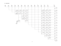
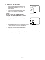
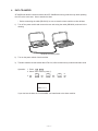
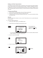
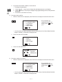
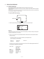
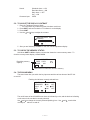
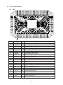
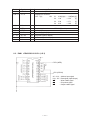
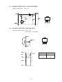
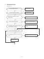
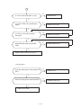
(with price)
SF-4300B(LX-588)
MAR. 1994
SF-4300B
R
CONTENTS
1.
SCHEMATIC DIAGRAM .................................................................................................... 1
1-1. MAIN PCB .................................................................................................................. 1
1-2. KEY MATRIX ............................................................................................................. 2
2.
SPECIFICATIONS ............................................................................................................. 3
3.
TO REPLACE THE BATTERIES....................................................................................... 5
4.
DATA TRANSFER ............................................................................................................. 6
5.
OPERATION REFERENCE ............................................................................................. 10
5-1. RESET OPERATION ............................................................................................... 10
5-2. TO ADJUST THE DISPLAY CONTRAST ............................................................... 11
5-3. TO CHECK THE MEMORY STATUS ...................................................................... 11
5-4. THE SOUND MENU ................................................................................................. 11
6.
LSI, IC (Pin function) ...................................................................................................... 12
6-1. CPU .......................................................................................................................... 12
6-2. RAM:µPD43256G-101215LL (LSI3) ........................................................................ 13
6-3. VOLTAGE REGULATOR:S-81253SGUP (REG1) .................................................. 14
6-4. VOLTAGE DETECTOR:S-80752AN (DET1) ........................................................... 14
7.
TROUBLESHOOTING ..................................................................................................... 15
8.
HARD CHECK ................................................................................................................. 18
9.
ASSEMBLY VIEW ........................................................................................................... 23
10. PARTS LIST .................................................................................................................... 25
1.
SCHEMATIC DIAGRAM
1-1. MAIN PCB
—1—
1-2. KEY MATRIX
—2—
2.
SPECIFICATIONS
Data storage:
Storage and recall of telephone, memo, schedule, reminder data; calendar display; secret area; editing;
memory status display.
Clock:
World time; reminder alarm; schedule alarm; daily alarm; accuracy under normal temperatures: ±3
seconds average.
Calculation:
10-digit arithmetic calculations; arithmetic constants (+, –, ×, ÷); independent memory; percentages;
square roots; 20-digit approximations; date calculations; other mixed calculations.
General:
Display element:
16-column × 4-line LCD
Memory capacity:
32 KB (28579 bytes)
Main component:
LSI
Power supply: 2 lithium batteries (CR2032)
Power consumption: 0.05W
Battery life:
Approximately 500 hours continuous operation in Telephone Directory
Approximately 400 hours repeating one minute of input and 10 minutes of display in Telephone
Directory
Approximately 12 months for memory back up
Test condition: 20°C
Auto power off:
Approximately 6 minutes after last key operation
Operating temperature: 0°C ~ 40°C (32°F ~ 104°F)
Dimensions:
Unfolded:
9.6H × 122W × 158.5Dmm (3/8"H × 4 3/4"W × 6 1/4"D)
Folded:
12.4H × 122W × 81.5Dmm (1/2"H × 4 3/4"W × 3 1/4"D)
Weight:
89g (3.1 oz)
Current consumption:
Power switch
TYP. [µA]
MAX [µA]
OFF
4.85
10.0
ON
225
380
Storage Capacity:
The 32K bytes memory capacity includes a 28579 bytes user area. The following shows examples
of what this means for the storage of data in each mode.
Telephone Directory:
Approximately 1360, under the following conditions:
Approximately 680, under the following conditions:
—3—
8-character name
10-character telephone number
8-character name
10-character telephone number
20-character address
Memo:
Approximately 1290, 20-character memos
Schedule Keeper:
Approximately 890, under the following conditions:
1 item per day, 20 characters per item
30 days per month
Starting time specified, alarm time set
Approximately 1020, under the following conditions:
1 item per day, 20 characters per item
30 days per month
Starting time specified, no alarm time
Reminder:
Approximately 1680, under the following conditions:
Approximately 1900, under the following conditions:
—4—
10 characters per item
Alarm time set
10 characters per item
No alarm time
3.
TO REPLACE THE BATTERIES
Screw
1) Loosen the screw on the back of the SF-4300B that
holds the battery compartment cover in place, and
remove the cover.
2)
Loosen the screw that secures one of the two battery
holders in place and remove the battery holder.
RESET
Caution
Be sure to remove only one battery at a time.
Otherwise, you will lose all data stored in memory.
3)
Replace the old battery with a new one, making sure
that the positive (+) side of the new battery is facing up
(so you can see it).
4)
Replace the battery holder and secure it by tightening its screw.
• Be sure careful that you do not over tighten the screw.
5)
Repeat steps 2) through 4) for the other two batteries.
• Be sure to replace all two batteries. Never mix old batteries with new ones, and be sure to use
CR2032 lithium batteries only.
6)
After you replace all two batteries, replace the battery compartment cover and secure it by tightening
its screw.
• Be careful that you do not over tighten the screw.
—5—
4.
DATA TRANSFER
SF-4300B can transfer customers data to other SF-4300B with memory protection only when replacing
the LCD or the outer case. How to transfer the data.
* Before connecting the cable (SB-60/62), be sure to reset the slave machine to clear all data.
1)
Turn off the power switch and connect the two units using the cable (SB-60/62) as shown in the
drawing.
SB-60/62 accessory cable
2)
Turn on the power switch of each machine.
3)
The slave machine must be set the date of Feb. 3rd, 1901 into the memory under the calculator mode.
Operation: 1. Press ON MENU
2. Select "CAL" mode or press 6.
3.
1
TIME
DATE
TIME
DATE
2
M
3
TIME
DATE
M+
R
SUN
1901/ 2/ 3
If you don't set the date, the "PASSWORD" isn't transferred to the slave machine.
—6—
Setting up for Data Communications
The following procedures describe what you should do to set up for data communications between
two SF Units or between an SF Unit and a personal computer. In addition to hardware connections,
it details how to set up the communications parameters and how to set up the SF-4300B to receive
data. By following these instructions carefully, you can be ensured of successful communications
every time.
To connect two SF Units
1.
2.
3.
Check to make sure that the power of the two SF Units is switched off.
Remove the covers from the connectors on the two SF Units.
Connect the two SF Units using the optional SB-60/62 cable. You can also connect them using
an SB-60/62 cable.
Important
Be sure to replace the connector covers on the SF Units when you are not performing data
communications.
4)
Check the hardware parameters.
1. Select "TEL" mode or press 1 under MENU screen.
2.
Press FUNC twice to display the second function menu.
FUNC FUNC
1*
2
3
4
TO SECRET AREA
ALL DELETE
LABEL EDIT
DATA COMM
* If the password isn't
registered in the SF unit,
display shows X instead
of "1".
CAPS
• You can perform the above operation while the initial screen of the Memo Mode, Schedule
Keeper, Calendar, or Reminder is displayed also.
3.
Press 4 to select DATA COMM.
4
1
2
3
SEND
RECEIVE
SET UP PAR.
CAPS
4.
Press 3 to select SET UP.
3
✻✻ SET UP PAR. ✻✻✻
PARITY
E O N
BIT LENGTH 7 8
BPS
4800 9600
CAPS
—7—
• N is blinking.
5.
If the units have another condition, reset as above.
• To change the parameters
1.
2.
3.
SET
5)
Use the and — cursor keys to change the selected parameter on the display.
Use the and
cursor keys to change the high-lighted setting of the currently selected
parameter.
Press SET to store them in memory.
Set up the slave machine
1. While an initial screen is displayed, press FUNC twice to display the second function menu.
FUNC FUNC
1*
2
3
4
TO SECRET AREA
ALL DELETE
LABEL EDIT
DATA COMM
* If the password isn't
registered in the SF unit,
display shows X instead
of "1".
CAPS
• You can perform the above operation while the initial screen of the Memo Mode, Schedule
Keeper, Calendar, or Reminder is displayed also.
2.
Press 4 to select DATA COMM.
4
1
2
3
SEND
RECEIVE
SET UP PAR.
CAPS
3.
Press 2 to select RECEIVE.
2
DATA
RECEIVE OK
TO STOP
PRESS (ESC)
CAPS
6)
Set up the customer’s machine.
1. While an initial screen is displayed, press FUNC twice to display the second function menu.
FUNC FUNC
1*
2
3
4
TO SECRET AREA
ALL DELETE
LABEL EDIT
DATA COMM
* If the password isn't
registered in the SF unit,
display shows X instead
of "1".
CAPS
• You can perform the above operation while the initial screen of the Memo Mode, Schedule
Keeper, Calendar, or Reminder is displayed also.
—8—
2.
Press 4 to select DATA COMM.
4
1
2
3
SEND
RECEIVE
SET UP
CAPS
3.
Press 1 to select SEND.
1
1
2
3
ONE ITEM
MODE DATA
ALL DATA
- SEND -
CAPS
4.
Press 3 to select ALL DATA.
3
SEND ALL DATA?
SET/ESC
CAPS
5.
Press SET to start the send operation or ESC to abort the operation without sending anything.
SET or ESC
DATA
SENDING
TO STOP
PRESS (ESC)
CAPS
• Data is send in the sequence: Telephone Directory, Memo Mode, Reminder Mode, Schedule
Keeper, Calendar.
• To abort the send operation at any time, press ESC.
• If an error occurs during the send operation, the message “TRANSMIT ERROR!” appears on
the display. Press ESC to clear the error message.
6.
After the send operation is complete, the display returns to the initial screen of the mode you
were in when you started this procedure.
—9—
5.
OPERATION REFERENCE
5-1. RESET OPERATION
The following procedure erases all data stored in the memory of the SF Unit.
Perform the following operation only when you want to delete all data and initialize the settings
of the SF Unit.
Remember-you should always keep copies of important data by writing it down, by transferring
it to a personal computer or other SF Unit.
To reset the SF Unit's memory
RESET button
RESET
1. Switch on power and press the RESET button with a thin, pointed object.
ALL DATA
CLEAR!
OK?
Y/N
CAPS
Warning!
The next step deletes all data stored in the SF Unit's memory. Make sure that you really want
to delete the data before you continue!
2. Press Y* to reset the memory and delete all data or N to abort the reset operation without
deleting anything.
* Note that the letter key you press to indicate "yes" depends on the
system language, as noted below.
English: Y
French: O
Spanish: S
Italian: S
German: J
Following the reset operation described above, the Home Time display appears and the SF
Unit setting are initialized as noted below.
Home Time:
Zone:
World Time:
Daily Alarm:
Menu Mode:
Language:
12-hour format
JAN/1/1994
AM/12:00 00
London(LON)
New York(NYC)
12:00 PM
Telephone mode
English
— 10 —
Sound:
Character input:
Schedule alarm → ON
Reminder Alarm → ON
Daily alarm → OFF
Key → ON
CAPS
5-2. TO ADJUST THE DISPLAY CONTRAST
1 Enter the Telephone Directory Mode.
• You could enter any mode except the Calculator mode here.
2 Press SHIFT and confirm that the "S" indicator is on the display.
3 Press CONT.
4 Use the and keys to adjust the contrast.
✻✻✻✻ CONTRAST ✻✻✻✻
(LIGHTER)
(DARKER)
CAPS
5 After you are finished, press ESC to clear the contrast adjustment display.
5-3. TO CHECK THE MEMORY STATUS
Hold down SHIFT CAPA to display a screen that shows the current memory status. To
clear the memory status display, release CAPA.
Remaining memory
capacity
✻✻✻✻ CAPACITY ✻✻✻✻
FREE 27678
USED
901
3%
CAPS
Total number of characters stored in memory
5-4. THE SOUND MENU
The sound menu lets you switch the key input tone and the various alarms of the SF Unit
on and off.
Flashing dot indicates currently selected item
SCHED AL
REMINDER
DAILY AL
KEY
● ON
● ON
ON
● ON
OFF
OFF
● OFF
OFF
CAPS
Dot indicates on/off status
The on/off status of each SOUND menu items is indicated by a dot, and the dot that is flashing
on the menu is the one that is currently selected.
Use and to change the currently selected (flashing) item. Use and
to switch the
currently selected item on and off.
— 11 —
6.
LSI, IC (Pin function)
6-1. CPU
No.1
Pin No.
1~5
Signal
C0 ~ 4
I/O
Out
Function
Common Signal for display
6
GND
In
GND /0[V]
7,8
BZ1,2
Out
9
VDD
In
10
CSRA1
Out
Chip enable signal (Not used)
11
CSRA2
Out
Chip enable signal for RAM
12
CSROM
Out
Chip enable signal (Not used)
13
WEB
Out
Write enable signal for RAM
Buzzer terminal
Power supply/5.3[V]
14,15
RA15,16
Out
Address bus (Not used)
16 ~ 30
A0 ~ 14
Out
Address bus
31 ~ 38
IO0 ~ 7
I/O
Data bus
39 ~ 54
KY0 ~ 15
I/O
Key signal
55
SW
In
Battery switch (On: "L"/0[V]
56
DEBUG
-
Test for manufacturer
57
ON
58
CRCKI
In
59
SOUTB
Out
60
SIN
In
Transmission data input
61
VDD
In
Power supply/5.3[V]
62
TEST
-
Test for manufacturer
63
VTM
-
Not used
Out
Data communication enable
GND/0[V]
Transmission data output
— 12 —
Off: "H"/6[V])
Pin No.
64,65
67,69~71
Signal
I/O
OSC I/O
I/O
V1 ~ 4
Function
Clock terminal (DT-26S)
Voltage for LCD driver
OFF: 0[V]
68
NC
-
Not used
72
INTO
In
Low battery detection
73
STNT
-
GND/0[V]
74
VLCD
In
Power supply/5.3[V]
ON:
75 ~ 171
S0 ~ 95
Out
Segment signal for display
172 ~ 199
C5 ~ 32
Out
Common signal for display
168,200
NC
-
V1:
0.64(Light) ~ 1.29(Dark)[V]
V2:
1.29
~ 2.56
[V]
V3:
3.99
~ 2.71
[V]
V4:
4.64
~ 3.99
[V]
INTO<5.2[V]=> No power on
Not used
6-2. RAM: µPD43256G-101215LL (LSI 3)
CPU (WEB)
CPU (CSRA2)
A0 ~ A14 :
IO0 ~ IO7 :
WE
:
CS
:
OE
:
— 13 —
Address input signal
Data signal (Input/Output)
Write enable signal
Chip select signal
Output enable signal
6-3. VOLTAGE REGULATOR: S-81253SGUP (REG1)
Output Voltage (Vout) : 5.3V ± 5%
VIN 2
3
OUT
RA
+
–
RI
RB
VREF
1
2
3
GND Vin Vout
GND 1
6-4. VOLTAGE DETECTOR: S-80752AN (DET1)
Detection Voltage(–VDET) : 5.2V ± 2.5%
[5.07V (MIN) ~ 5.33V (MAX)]
2 VDD
1 OUT
1
2
3
Vout Vin GND
3 VSS
VDD
+VDET
–VDET
VDD
VDD
VSS
— 14 —
Input voltage
Output voltage
>5.2V
5V
<5.2V
0V
7.
TROUBLESHOOTING
< No power on >
N
Adjust contrast
Is contrast adjustment OK?
Y
N
Replace batteries
Is power of batteries enough?
Y
Y
Does display appear by pressing
Reset button?
Check other function
N
Y
Does it sound by key enter?
Refer to <No/Erratic display>
N
Do batteries make positive contact
with the battery springs?
N
Adjust contact and clean battery
spring
Y
Y
Is 3-pin of S-81253 (REG1) 5.3 [V]?
N
N
Are capacitor C8, C9, C10, C11,C12
OK?
Y
Replace REGT1
1
— 15 —
Replace C8, C9, C10, C11,C12
1
N
Replace DET1
Is 1-Pin of S-80752AN (DET 1) 5[V]?
Y
N
Is 11-Pin of CPU (LSI 1) sending the
signal?
Replace CPU (LSI1)
Y
N
Is 13-Pin of CPU (LSI1) sending
the signal?
Replace CPU (LSI1)
Y
N
Does RAM make positive contact with
PCB?
Resolder RAM (LSI3)
Y
Replace RAM (LSI3) or CPU (LSI1)
< No key input >
Does key make positive contact with PCB
Ass’y
N
Replace PCB
Y
Does CPU make positive contact with PCB?
N
Y
Replace CPU (LSI1)
— 16 —
Resolder CPU (LSI1)
< No/Erratic display >
N
Is input 2-Pin of S-81253 (REG1) 6[V]?
Check batteries
Y
N
Is output 3-Pin of S-81253 (REG1)
5.3[V]?
Replace REG1
Y
*
Are voltage of several capacitors enough?
V1:
V2:
V3:
V4:
N
1.3 [V]
2.5 [V]
2.7 [V]
3.9 [V]
Y
Check solder part of C6, C7, C8,
C9, C10 or replace.
*CONTRAST: MAX
N
Does CPU (LSI1) make positive contact with PCB?
Resolder
Y
Replace CPU (LSI1)
< High current consumption >
Y
Is there any short circuit?
Check PCB
N
N
Replace capacitors
Are the several capacitors OK?
Y
Resolder/Replace CPU, IC
— 17 —
8. HARD CHECK
No.
OPERATION
DISPLAY
1
Turn on while short the short pad
(KEY61).
SELF TEST PROG.
PRESS SEARCH
QUIT BY OFF
CASIO AUG. 1993
SEARCH
3
Main menu
1 DISP
MEMORY
KEY
BUZZER
I/F
DISP
1 WHITE
2 BLACK
3 CHECK.
4
5
6
7
RVS.
FRAME
DOT 4
TIME
Display check
1
4
No display
2
5
All dots display
3
6
Checker display
4
7
The short pad is located behind the
tape I.
2
3
4
5
TEST
MENU
2
1
NOTE
Reverse checker display
— 18 —
No.
OPERATION
DISPLAY
NOTE
5
8
FRAME
6
9
Dots appear at 4 corners.
TIME DISPLAY
10
7
00:00:00
ESC
TEST
MENU
2
3
4
5
11
1 DISP
12
3
13
2
HOME/WORLD MENU
OFF ON INS DEL
TIME/DATA DISP CHNG
14
Check if timer is
working.
KEY
MEMORY
KEY
BUZZER
EXT
1 RANDOM
2 AUTO
Key check
No display
00
01
02
...............
ESC .........................
FUNC ...................... P
CAPS ...................... SET
SHIFT ...................... SPACE
— 19 —
03
56
04
57
...............
• Check the key No.
appears on the
display.
• Check the key
sounds.
• To return to the
menu mode, enter
SEARCH .
No.
OPERATION
SEARCH
15
DISPLAY
TEST
MENU
2
3
4
5
1 DISP
4
BUZZER
MEMORY
KEY
BUZZER
EXT
1 BEEP
2 ALARM1
3 ALARM2
16
NOTE
Buzzer check
2
EXECUTING!!
17
ESC
BUZZER
1 BEEP
2 ALARM1
3 ALARM2
ESC
TEST
MENU
2
3
4
5
MEMORY
KEY
BUZZER
EXT
3
4
5
6
WR2
READ2
DUMP
CHKSUM
18
19
1 DISP
2
MEMORY
1 WR1
2 READ1
20
1
21
WRITE1
— 20 —
Check the alarm 1
sound.
RAM check
No.
OPERATION
(After few seconds)
22
DISPLAY
MEMORY
1 WR1
2 READ1
2
3
4
5
6
NOTE
WR2
READ2
DUMP
CHKSUM
EXECUTING
23
COMPLETE
32KB
24
ESC ESC
25
TEST
MENU
1 DISP
26
Press "RESET" key.
— 21 —
2
3
4
5
MEMORY
KEY
BUZZER
EXT
Check sound.
If RAM has defect,
error message will
be appeared.
— 23 —
9.
16
ASSEMBLY VIEW
25
17
10
6
7
12
JC1
27
27
X1
8
19
LSI
11
3
23
9
15
22
4
c11
c9
1
20
21
29
28
26
24
13
18
2
14
5
10.
PARTS LIST
N
Item
Code No.
N
N
N
N
N
LSI1
LSI3
Q1
DET1
REG1
C1~4
C5,6
C7
C8,10,12
C9,11
D1
D2
R4,20
R5
R6
R7
R8,9
R10
R13
X1
JC1
1
2
3
4
6409 2760
2011 2849
2259 0959
2105 3297
2105 3290
2896 1400
2845 2534
2845 2548
2845 1540
2805 0275
2390 2128
2390 0364
2797 2051
2791 1170
2797 0637
6510 4770
2797 1078
2791 1871
2797 2520
7110 0642
3501 6538
3335 4606
6409 6270
6409 6300
6409 6310
N
5
6409 6090 PCB ass'y
DB20XX0300V*1
(This ass'y contains the above parts as its element.)
N
N
N
N
6
7
7
8
9
10
11
12
13
14
15
16
17
18
19
20
21
22
23
24
25
26
3122 2380
6409 6200
6410 8340
6409 6210
6510 4440
6510 4500
6512 1080
6408 5920
6409 6220
6409 6230
6409 6120
6409 6130
6409 6140
6409 6150
6409 6160
6409 6170
6409 6180
6409 6190
6510 4310
6510 4350
6511 7160
6511 8400
Notes: N
M
R
Q
N
N
N
N
N
N
N
N
N
N
N
N
N
N
Parts Name
Specification
COB LSI
LSI (RAM)
Chip digital transistor
CMOS IC
Regulator
Chip capacitor
Chip capacitor
Chip capacitor
Chip capacitor
Electrolytic capacitor
Chip diode
Schottky diode
Chip resistor
Chip resistor
Chip resistor
Chip resistor
Chip resistor
Chip resistor
Chip resistor
Crystal oscillator
Jack
LCD
Heat seal
Battery contact spring (+)
Battery contact spring (–)
C312133*1
uPD43256AGU-1012LL
DTC114YKT-146
S-80752AN-JG-T1
S-81253SGUP-DIJ-T1
C1608JF1C334Z-TP
MCH185A180JK
MCH183F104ZK
MCH212F104ZK
CE04C-1A100MS5
MA740-(TX)
MA713-TX
ERJ-3GEY0R00
ERJ-6GEYJ182
ERJ-6GEYJ473
CC1001311C0
ERJ-6GEYJ101
ERJ-6GEYJ474
ERJ-3GEAK206V
DT-26S
HSJ1169-012010
CD418-TS
FX200P40056
EF01DB20102
EF02DB10100
Buzzer
Lower case
Lower case (USA,CANADA)
Battery change label
Insulation seal
Buzzer tape
Nut
Switch knob ass'y
Battery cover
Battery cover label
Battery holder
Display panel
Knob
Battery insulation
Mask tape
Rubber key
Upper case
Cushion
Screw
Screw
RB Insert
Key contact rubber
– New parts
– Minimum order/supply quantity
– Rank
– Quantity used per unit
EFB-S55C41A8
FABDB201004
FABDB201012
HGC00001102
HGFC0001206
HGFC0000501
MD100000602
DB2AXX4A00M*1
FADDB201001
HGC00001200
ECDB1011108
EL5G0009107
FB3DB201001
EL4C0001105
HGG00012808
LADB2010001
FAADB201008
FH100027108
MAA80006311
MAA80006302
LC120000102
LADB0220105
— 25 —
1
1
1
1
1
5
2
1
3
2
1
1
1
1
1
1
2
1
1
1
1
1
1
2
2
1
1
20
10
5
20
20
20
20
20
20
20
20
20
20
20
20
20
20
1
20
1
5
20
20
FOB Japan
N.R.Yen
Unit Price
1,010
600
12
47
60
10
4
6
4
21
50
33
2
3
2
5
3
3
2
57
56
350
82
16
16
1
1
3,060
Q M
R–A:
B:
C:
X:
R
A
B
B
B
B
C
C
C
C
C
C
C
C
C
C
C
C
C
C
B
C
A
A
C
C
A
1 10
36
C
1 5
61
X
1 5
70
X
1 20
7
X
3 20
6
X
1 10
17
X
3 20
15
X
1 10
30
C
1 20
29
X
1 20
16
X
2 20
26
X
1 10
48
C
1 20
13
X
1 10
27
X
1 20
7
X
1 1
200
C
1 1
120
C
2 20
10
X
2 20
3
C
1 20
2
B
1 10
17
B
1 10
10
C
Essential
Stock recommended
Others
No stock recommended
N
Item
N
N
N
27
28
29
Code No.
Parts Name
6512 0980 Screw
6409 6240 Hard case
6409 6250 Label
Notes:
N
M
R
Q
–
–
–
–
FOB Japan
N.R.Yen
R
Unit Price
8 20
2
X
1 5
78
X
1 1
130
X
Specification
Q M
MAB20086306
FC1DB20001
HGG00012603
New parts
Minimum order/supply quantity
Rank
Quantity used per unit
— 26 —
R–A:
B:
C:
X:
Essential
Stock recommended
Others
No stock recommended
MA0600741A