1
REV.-A
CHAPTER 1
GENERAL DESCRIPTION
(
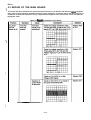
1.1 FEATURES . . . . . . . . . . . . . . . . . . . . . . . . . . . . . . . . . . . . . . . . . . . . . . . . . . . . . . . . . . . . . . . . . .
1-1
1.2 SPECIFICATIONS . . . . . . . . . . . . . . . . . . . . . . . . . . . . . . . . . . . . . . . . . . . . . . . . . . . . . . . . . . . . .
1-3
1.2.1 Hardware Specifications . . . . . . . . . . . . . . . . . . . . . . . . . . . . . . . . . . . . . . . . . . . . . . . . . . . . . . 1-3
1.2.2 Firmware Specifications . . . . . . . . . . . . . . . . . . . . . . . . . . . . . . . . . . . . . . . . . . . . . . . . . . . . . .
1-9
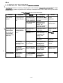
1.5 DIP SWITCHES-AND JUMPER SETTING . . . . . . . . . . . . . . . . . . . . . . . . . . . . . . . . . . . . . . . . . . . 1-18
1.5.1 DIP Switch Settings . . . . . . . . . . . . . . . . . . . . . . . . . . . . . . . . . . . . . . . . . . . . . . . . . . . . . . . 1-18
1.5.2 Jumper Setting . . . . . . . . . . . . . . . . . . . . . . . . . . . . . . . . . . . . . . . . . . . . . . . . . . . . . . . . . . . 1-19
1.5.3 Dip Switch Setting for IBM emulation mode . . . . . . . . . . . . . . . . . . . . . . . . . . . . . . . . . . . . 1-20
1.7 MAIN COMPONENTS . . . . . . . . . . . . . . . . . . . . . . . . . . . . . . . . . . . . . . . . . . . . . . . . . . . . . . . . . 1-26
1.7.1 C107 MAIN Board (Main Control Circuit Board) . . . . . . . . . . . . . . . . . . . . . . . . . . . . . . . . . . 1-26
1.7.2 C062 PNL Board (Control Panel Circuit Board) . . . . . . . . . . . . . . . . . . . . . . . . . . . . . . . . . . 1-27
1.7.3 C062 PSB/PSE Board (Power Supply Circuit Board) . . . . . . . . . . . . . . . . . . . . . . . . . . . . . . 1-27
1.7.4 Printer Mechanism (M-5J1O) . . . . . . . . . . . . . . . . . . . . . . . . . . . . . . . . . . . . . . . . . . . . . . . . . 1-28
1.7.5 Housing . . . . . . . . . . . . . . . . . . . . . . . . . . . . . . . . . . . . . . . . . . . . . . . . . . . . . . . . . . . . . . . . 1-28
LIST OF FIGURES
Figure 1-1. Exterior View of the LQ-570+ . . . . . . . . . . . . . . . . . . . . . . . . . . . . . . . . . . . . . . . . . . . . .
Figure 1-2. Pin Configuration . . . . . . . . . . . . . . . . . . . . . . . . . . . . . . . . . . . . . . . . . . . . . . . . . . . . . . .
Figure 1-11. LQ-570+ Component Layout . . . . . . . . . . . . . . . . . . . . . . . . . . . . . . . . . . . . . . . . . . . . .
Figure 1-12. C107 MAIN Board . . . . . . . . . . . . . . . . . . . . . . . . . . . . . . . . . . . . . . . . . . . . . . . . . . . . .
Figure 1-13. C062 PNL Board . . . . . . . . . . . . . . . . . . . . . . . . . . . . . . . . . . . . . . . . . . . . . . . . . . . . . .
Figure 1-14. C062 PSB/PSE Board . . . . . . . . . . . . . . . . . . . . . . . . . . . . . . . . . . . . . . . . . . . . . . . . . .
Figure 1-15. Model-5J10 Printer Mechanism . . . . . . . . . . . . . . . . . . . . . . . . . . . . . . . . . . . . . . . . . . .
Figure 1-16. Housing . . . . . . . . . . . . . . . . . . . . . . . . . . . . . . . . . . . . . . . . . . . . . . . . . . . . . . . . . . . .
1-2
1-3
1-26
1-26
1-27
1-27
1-28
1-28
LIST OF TABLES
(
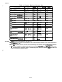
Table 1-1. Interface Options . . . . . . . . . . . . . . . . . . . . . . . . . . . . . . . . . . . . . . . . . . . . . . . . . . . . . . . . 1-1
Table 1-2. Optional Units . . . . . . . . . . . . . . . . . . . . . . . . . . . . . . . . . . . . . . . . . . . . . . . . . . . . . . . . . . 1-2
Table 1-3. Specifications for Cut Sheets . . . . . . . . . . . . . . . . . . . . . . . . . . . . . . . . . . . . . . . . . . . . . . 1-5
Table 1-4. Specifications for Cut Sheeta (Carbonless Duplicating Paper) . . . . . . . . . . . . . . . . . . . . . 1-5
Table 1-6. Specifications for Continuous Sheets . . . . . . . . . . . . . . . . . . . . . . . . . . . . . . . . . . . . . . . . 1-5
Table 1-6. IEnvelopes . . . . . . . . . . . . . . . . . . . . . . . . . . . . . . . . . . . . . . . . . . . . . . . . . . . . . . . . . . . . . . 1-5
Table 1-7. ILabels Specifications . . . . . . . . . . . . . . . . . . . . . . . . . . . . . . . . . . . . . . . . . . . . . . . . . . . . . 1-5
Table 1-8. IPrinting (Text Mode) . . . . . . . . . . . . . . . . . . . . . . . . . . . . . . . . . . . . . . . . . . . . . . . . . . . . 1-1o
Table 1-9. IPrinting (Bit Image Mode) . . . . . . . . . . . . . . . . . . . . . . . . . . . . . . . . . . . . . . . . . . . . . . . . . 1-11
Table 1-10. Character Matrix and Character Size . . . . . . . . . . . . . . . . . . . . . . . . . . . . . . . . . . . . . . . 1-12
Table 1-12. Settings for DIP Switch 1 (SWl)(ESC/P 2) . . . . . . . . . . . . . . . . . . . . . . . . . . . . . . . . . . . 1-18
Table 1-13. Settings for DIP Switch 2 (SW2)(ESC/P 2) . . . . . . . . . . . . . . . . . . . . . . . . . . . . . . . . . . . 1-18
Table 1-14. International Character Set Selection . . . . . . . . . . . . . . . . . . . . . . . . . . . . . . . . . . . . . . . 1-19
Table 1-15. Page Length . . . . . . . . . . . . . . . . . . . . . . . . . . . . . . . . . . . . . . . . . . . . . . . . . . . . . . . . . 1-19
Table 1-16. Settings for DIP Switch 1 (SW1)(IBM Emulation Mode) . . . . . . . . . . . . . . . . . . . . . . . . . 1-20
Table 1-17. Settings for DIP Switch 2 (SW2)(IBM Emulation Mode) . . . . . . . . . . . . . . . . . . . . . . . . . 1-20
Table 1-18. Code Selection . . . . . . . . . . . . . . . . . . . . . . . . . . . . . . . . . . . . . . . . . . . . . . . . . . . . . . . 1-20
.
1’
REV.-A
/’
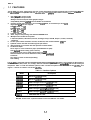
1.1 FEATURES
The LQ-570+ is a small, light-weight, low-cost, printer with advanced paper handling that is upper corrmatible with
the LQ-510/550 and compatible with the LQ-570/1070. The printets main features areas folbws:
1.
2.
3.
4.
5.
6.
7.
8.
9.
Use of ESC/P 2 control codes
Ability to print multi-point fonts
Ability to receive and print raster graphic images
Compatibility with the LCVSQ series available on the market
Printing speeds: 225 characters per second (cps) (draft, 10 characters per inch (cpi))
High speed drafl has not equiped
269 cps (draft, 12 cpi)
225 cps (draft, 10 cpi)
90 cps (LQ, 12 cpi)
75 cps (LQ, 10 cpi)
Optional interface card
Clear, easy-to-read printing with standard EPSON fonts
Multiple fonts resident in the printer
9 LQ fonts (Roman, Saris Serif, Courier, Prestige, Script, OCR-B, Script C, Orator, Orator-S)
1 draft font
Control panel switch selection of fonts, mndensed, and cut-sheet feeder (CSF) bin
Optional tractor unit that can make up push-pull tractor
Easy handling of cut sheets with the optional cut-sheet feeder
Continuous Paper
Three ways to ‘insert continuous paper (front/bottom/rear path)
Auto backout & auto loading (rear insertion)
Continuous paper can be used without removing CSF
Standard tractor unit can be attached in two position (pusWpull)
Cut Sheet
Two ways to insert cut sheets (front/top)
Auto loading
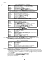
The LQ-570+ is equipped with the standard EPSON 8-bit parallel interface( Printing is not possible for the following
baud rates: 1800, 200, 134.5, 110, 75 bps). Various interface options ensure mmpatibility with a wide variety of
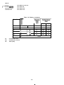
computers. Table 1-1 lists the interface options, Table 1-2 lists the optional units available for the LQ-570+, and
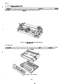
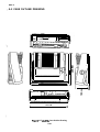
Figure 1-1 shows an exterior view of the LQ-570+.
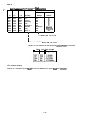
Table 1-1. Interface Options
Model
Description
C82305
Serial l/F card(inch screw)
C82306
Serial l/F card(mm screw)
C82307
32KB intelligent serial l/F card(inch screw)
C82308
32KB intelligent serial l/F card(mm screw)
C8231O
32KB intelligent pararell I/F card(inch screw)
C82311
32KB intelligent pararell l/F card(mm screw)
I C82313
I
I 32KB IEEE-488 l/F card
NOTES : Refer to the “Optional Interface Technical Manual” for details.
1-1
I
REV.-A
1
I
Model
Table 1-2. Optional Units
Description
C806371(EAI ver.) I Single-bin cut sheet feeder(80-column)
C806372(others)
I Single-bin cut sheet feeder(80-column)
C806381(EAI ver.) I High-capacity cut sheet feeder(80-column)
C806382(others)
I High-capacity cut sheet feeder(80-column)
C800191(EAI ver.) I Tractor unit(80~lumn)
C800192(others) I T r a c t o r unit(80adumn)
7753
I Fabric ribbon cartridge(80-column)
7768
I Fabric ribbon cattridae(80-column)
6
Figure 1-1. Exterior View of the LQ-570+
1-2
REV.-A
~- 1.2 SPECIFICATIONS
This section provides specifications for the LQ-570+ printer.
1.2.1 Hardware Specifications
Printing method
Pin mnfiguration
Serial, impact, dot matrix
24 wires (12x 2 staggered, diameter 0.2 mm)
Wires 2
~;
It
Wires 1
1
I
I
I
/+
I
I
i
I
I
Feeding methods
Line spacing
Paper insertion
Paper-feed speed
Friction feed (front/top)
Push tractor feed (rear)
Pull tractor feed (fronthttom)
Push-pull tractor feed (with optional tractor) (rear)
1/6 inch, 1/8, or programmable in units of 1/360 inch
Friction feed -- Front or rear side
Tractor feed -- Front, bottom, or rear side
Friction without CSF -2.0 msec/O.141mm(continuous)
60.Oms/4.23mm(continuous 2.81PS)
65.2ms/4.23mm(intewal 2.81PS)
2.20mst0.141 mm(continmus)
Friition with CSF -66.7rns/4.23mm(mntinuous 2.51PS)
73.1 ms/4.23mm(intewal 2.51PS)
2. Oms/O.141 mm(continuous normal mode)
Tractor -60.Orns/4.23mm(continuous normal mode 2.81PS)
65.2ms/4.23mm(intetval normal mode 2.81PS)
2.5ms/O.141 mm(copy mode)
75.Oma/4.23mm(copy mode 2.21PS)
80.6ms/4.23mm(copy mode 2.21PS)
NOTE: The points below provide precautions for paper handling.
1. Friction feed(release lever in FRICTION POSITION).
. Paper must be loaded from the front or top entrance.
c Do not use continuous paper.
s Do not perform any reverse paper feeds within the top 8.5 mm(.34in.),bottom 22 mm(.87in.)
(top entrance), or bottom 40.2mm(l .6in.)cfront entrance) area.
c Do not perform any reverse feeds greater than 1/6 inch after a paper end has been detected.
1-3
REV.-A
Table 1-3. Specifications for Cut Sheets
(
Width
Length
Thickness
Weight
Quality
148 mm to 257 mm (5.8 in. to 10.1 in.) (top insertion)
182 mm to 257 mm (7.2 in. to 10.1 in.) (front insertion)
364 mm (14.3 in.), maximum
0.065 mm to 0.14 mm (0.0025 in. to 0.0055 in.)
14 lb to 24 lb (52.3 g/m’*2 to 90 g/m**2)
plain paper or recycled paper(under normal temperature)
Table 1-4. Specifications for Cut Sheets (Carbonless Duplicating Paper)
Width
Length
Thickness
Weight
Quality
Copies
182 mm to 216 mm (7.2 in. to 8.5 in.)
257 mm to 297 mm (10.7 in. to 11.7 in.)
0.12 mm to 0.32 mm (0.0047 in. to 0.012 in.)
12 lb to 15 lb (40 g/m**2 to 58 g/m**2)
Carbonless duplicating paper
4 sheets (1 original and 3 copies)
Table 1-5. Specifications for Continuous Sheets
Width
Copies
Quality
Thickness
Weight
101 mm to 254 mm (4.0 in. to 10.0 in.)
4 sheets (1 original and 3 copies)
plain or carbonless multi-part paper
recycled paper(under normal temperature)
0.065 mm to 0.10 mm (0.0025 in. to 0.0039 in.) - single sheet
0.065 mm to 0.32 mm (0.0025 in. to 0.012 in.) - total
14 lb to 22 lb (52.3 g/m**2 to 82 g/m**2) - single sheet
12 lb to 15 lb (40 g/m**2 to 58 g/m**2) - each
Table 1-6. EnveloDes
Size
Copies
Thickness
Weight
Quality
NOTES :
No. 6 166 mm x 92 mm
No. 10 240 mm x 104 mm
Not available
0.16 mm to 0.52 mm (0.0063 in. to 0.0197 in.)
Differences in thickness within the printing area must be less than
0.25 mm (0.0098 in.)
12 lb to 24 lb (45 g/m**2 to 91 g/m**2)
Bond paper, plain paper, airmail
a. Printinci on envelopes is available only at normal temperatures and only using top insertion.
b. Keep tie longer side of the envelope-horizontal during insertion.
c. Place the left edge of a No. 6 envelope at the sheet guide setting mark.
Table 1-7. Labels Specifications
Label size
Copies
Thickness
2 1/2 in. x 15/16 in.
4 in. x 15/16 in.
4 in. x 17/16 in.
Not available
0.07 mm to 0.09 mm (0.0028 in. to 0.0031 in.) - base paper
0.16 mm to 0.19 mm (0.0063 in. to 0.0075 in.) - total
NOTES: a. Printing on labels is available only at normal temperatures.
b. Labels must be of the fanfold type.
c. Labels with pressure sensitive paper must be pasted along the perforation and tractor holes and the
total thickness must be less than or equal to 0.3 mm (0.0118 in.). Labels can be printed out only if
the temperature is between 5 and 36 degrees C (41 and 95 degrees F) and humidity is between
10 O/. and 80 YO RH.
AVERY CONTINUOUS FORM LABELS
d. Recommendation
AVERY MINI-LINE MBELS
f. Labels must be used with the pull tractor unit (front or button)
g. Do not perform reverse feeds.
1-5
I
REV.-A
(
220240 V version Rated voltage 220 to 240 VAC
Input voltage range 198 to 264 VAC
Rated frequency
50 to 60 Hz
Input frequency
49.5 to 60.5 Hz
Rated current
1.0 A
Power consumption Approx. 33W(during a self-test in draft mode,10 cpi)
Insulation resistance 10 megohms, minimum(at 500 VDC between AC Iines and chassis).
Dielectric strength
1250VAC rms 1 minute or 1500VAC rrns 1 second(between AC line
and chassis)
Environmental
Temperature range 5 to 35 degrees C (41 to 95 degrees F) -- operting
-30 to 60 degrees C (-22 to 140 degrees F) -- in shipment container
Humidity
10 to 80% RH - operating
5 to 857. RH -- storage
Resistance to shock IG, within IMS -operating
2G, within lms - storge
Resistance to
0.25 G, 55 Hz,Msx. - operating
Vibration
0.50 G, 55 Hz,Msx. -- storge
Physical specifications Weight
Dimensions
6.8 kg,approx(15 Ib.,approx.)
434mm(width) x 368mm(depth) x 160mm(height)
17.4 in.(width) x 14.7 in.(depth) x 6.3 in.(height)
1-8
REV.-A
(’
1.2.2 Firmware Specifications
Control code
EPSON ESC/P 2( ESWPTM level 2: EPSON new control code for printers)
IBM emulation mode (European version only)”l
NOTE: ● 1 :The European version is equipped with the IBM emulation mode, Please refer
to the emulation mode specification for details.
Printing direction
Input data buffer
Character code
Character tables
Fonts and pitches
Bit-map fonts.
Scalable fonts
Printing modes
Bidirectional with logic seeking
8KB (when SW 1-7 is OFF)
OKB (when SW 1-7 is ON)
ESC( A nL nH data... Print data as characters
Italic character table, PC 437, PC 850, PC 880, PC 883, PC 885, PC437*, PC851*
PC853*, PC852*, PC85~, PC889*, PC881*, BRACll~, Abicomp**
*:Available on the European version only
● *available on the other versions only
10, 12, 15, proportional
EPSON Roman
EPSON Saris-serif 10, 12, 15, proportional
EPSON Courier
10, 12, 15
10, 12
EPSON Prestige
EPSON Script
10, 12
EPSON Script C
proportional
OCR-B
10
EPSON Orator 10
EPSON Orator-S 10
10, 12, 15
EPSON Draft
8 pt to 32 pt
EPSON Roman
EPSON Saris-serif 8 pt to 32 pt
Selection and mixture of the following modes are allowed, excluding 15 cpi condensed
mode:
o Print quality (draft/letter quality)
o Character pitch (10, 12, 15, or proportional)
o Condensed
O Double-width
o Double-height
o Emphasized
o Double-strike
o Italic
o Underlined
o Double-underlined
o OverScore
o Strike-through
o Outline
o Shadow
1-9
REV.-A
See tables 1-8 and 1-9.
See Table 1-8.
See Table 1-10.
See Table 1-10.
Printing speed
~ printing COlumns
Character matrix
Character size
Table 1-8. Printing Text Mode)
Print Pitch
10
T
m
I
80
10
225
75
on
I
137
17.1
192
128
12
269
90
20
225
154
15
337
112
-
cpi:
Cps:
LQ:
LQ
off
12
15
Draft
off
1120
on
I
Invalid
characters per inch
characters per second
letter quality
1-1o
I
REV.-A
Table 1-9. Printing (Bit Image Mode)
Pins
Density
(dpi)
Bit Image Printing Mode
Printable Dots
Printing Speed
(ips)
8
Single-density
60
480
22.5
8
Dual-density
120
960
11.2
8
Double-speed, dual-density
120
960
22.5
8
Quadrupledensity
240
1920
11.2
8
CRT graphics
80
640
11.2
8
CRT graphics II
90
720
15.0
24
Single-density
60
480
22.5
24
Dual-density
120
960
11.2
24
CRT graphios II
90
720
15.0
24
Tripledens”~
180
1440
7.5
24
Hexdensity
360
2880
7.5
dpi: dots per inch
ips: inches per second
,
1-11
REV.-A
Table 1-10. Character Matrix and Character Size
(“
Printing Mode
Face Matrix
HDD
Character S&e
Unit ESC sp
Draft, 10 pitch
9 x 22
120
1.9 x 3.1
120
Draft, 12 pitch
9x22
120
1.9 x 3.1
120
Draft, 15 pitch
7 X 16
120
1.0 X 2.3
120
Draft, 10 pitch, mndensed
------
240
-------
120
Draft, 12 pitch, oondensed
------
240
. . . . . ..
120
LQ, 10 pitch
31 x 22
360
2.2 x 3.1
180
LQ, 12 pitch
27X 22
360
1.9 x 3.1
180
LQ, 15 pitch
22
X
360
1.6 X 2.3
180
LQ, 10 pitch, condensed
----
360
-——
180
LQ, 12 pitch, condensed
—--
360
“—
180
LQ, proportional
Max. 37X 22
Min. 18x 22
360
360
2.6 X 3.1
1.0 x 3.1
180
LQ, proportional, mndensed
. . . ..
------
360
360
..-.-.
---—
180
LQ, proportional,
super/subscript
Max. 28X 16
Min. 12x 16
360
360
1.8 X 2.3
0.7 X 2.3
180
LQ, pmpottional,
super/subscript, mndensed
----------
360
.......
180
16
360
...--.
NOTES: * HDD is horizontal dot density in dots per inch.
* Face matrii and character size indicate the size of the maximum character. This value is dependent
on paper, ribbon, etc.
* Unit ESC sp (which also can be sent as unit, followed by the character string CHR$(&h20)), indicates
the minimum length to be added to the right of the character speoified with the ESC sp control code.
● u
----’ indicates that the character matrix is reshaped by printer firmware. Character w“dth becomes half
of the noncondensed character width.
( “
1-12
REV.-A
~-
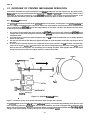
1.5 DIP SWITCHES AND JUMPER SETTING
This section describes the DIP switch selections and jumper setting for the LQ-570+ printer.
1.5.1 DIP Switch Setting for ESC/P 2 mode
This printer is”equipped with two banks of DIP-SWITCHES and they are located on the control panel. The tablel -12
through 1-15 shows the available function settings of two DIP switches. (Note that the status of the DIP switches
is only read at power on or upon receipt of the /lNIT signal.)
Table 1-12. Settinas for DIP Switch 1 EW1)
Description
No.
OFF
ON
Factory
Setting
See the table 1-14
1
2
International character set and PC
table selection
ON
ON
OFF
3
I
Italic
OFF
Unidir.
Bidir.
OFF
Comand Ianguage’1
IBM
ESC/P2
OFF
7
Inmd buffer
OKB
8KB
OFF
8
l-inch skip perforations
ON
OFF
OFF
4
Character table selection
5
Graphic print direction
6
GraDhic
NOTE: : *1 is European version only. The switch of 1-6 is invalid for another versions.
Table 1-13. Settings for DIP Switch 2 (SW2)
1
ON
Description
No.
Page length of continuous paper
OFF
See Table 1-15 below.
2
Factory
Setting
OFF
OFF
3
Auto tear-off
ON
OFF
OFF
4
Auto LF
ON
OFF
OFF
1-18
REV.-A
f
Tdda
. ---- 1.14.
. . . Intamational
. .. .----- —--— Character
--—- .–.
*t ~ktion
Table
1-3
Country
1-1
1-2
ON
ON
ON
Us.
ON
ON
ON
OFF
OFF
OFF
OFF
ON
OFF
OFF
ON
ON
OFF
OFF
OFF
ON
OFF
ON
OFF
ON
OFF
France
Germany
U.K.
Denmark 1
Sweden
Italy
Spain 1
1I
Others
Europe
437
850
860
863
665
437Greek
653
852
+
+
+
+
B~-SCll
Ab.komp
437
1I
I
I
I
I
i
----......
I
-— When SW 1-4 is ON.
- - . . — . - When SW 1-4 is Off.
NOTE: ● is not available on the European version(P0437 is selected).
)
Table 1-15. Page Length
1
1
2-1 I 2-2 ! Page Length
,
.m
I
1.5.2 Jumper Setting
Jumper 12 : Connect it to the “SLIN” to use the “SELECT IN” signal fmm host oomputer.
1-19
I
REV.-A
(’
1.5.2 DIP Switch Setting for IBM emulation mode
In the IBM emulation mode, with the DIP awitch 1-6 to ON, some other awitches are recognized by the printer in
different meanings from the ESC/P 2 mode.
Please refer to the emulation mode specif.=tion for details.
Table 1-16. Setting for DIP Switch 1
I
Description
No.
I
u
I 2I
I
1
3
Setting
See the table 1-14
set 2
Graphic print direction
!
Unidir.
Comand language
!
IBM
Input data buffer size
!
oKB
I 8 I AGM(Alternate Grafic Mode)
I
5
6
I
1
7
Character set selection
!
OFF
Setl
!
OFF
Bidir.
!
OFF
ESCIP2
!
OFF
8KB
I
OFF
,
!
1
k
ON
I
!
4
Factory
I
Code page selection
I
I
I
OFF
ON
t
ON
!
i
!
I
OFF
i
OFF
Table 1-17. Settinas for DIP Switch 2 (SW2)
Description
No.
T
1-2
ON
ON
ON
ON
OFF
ON
OFF
ON
OFF ON
OFF ON
OFF OFF
OFF OFF
OFF
Factory
Setting
12 inch
11 inch
OFF
valid
invalid
OFF
1
Page length of continuous from
2
Auto-CR
3
Auto tear-off
ON
OFF
OFF
4
Auto LF
ON
OFF
OFF
Table 1-18. Code page Selection
1-1
ON
1-3
ON
OFF
ON
OFF
ON
OFF
ON
OFF
Code page
437
850
660
663
665
437Greek
653
652
1-20
REV.-A
(-
1.6.11 Printer Protection for Heavy-Duty Printing
This printer has a printhead protection function to prevent it from overheating and to handle the printer when the
head driver voltage drops. If head temperature exceeds its maximum value, printing stops automatically until the
head temperature drops to a certain value before printing resumes. Printing resumes at a lower print speed at first.
However, as the head temperature decreases, print speed increases to normal speed automatically. If the head
temperature continues to increase at the lower speed, printing is stopped or resumed as temperature increases or
decreases.
If the voltage supplied to the head drive circuit drops below its minimum limit as a result of heavy-duty printing,
printing is interrupted immediately. When the power supply voltage recovers to a certain level, the remaining print
line is printed at hatf speed. This protective action occurs when half or more of the wires are activated mntinuously.
1-25
REV.-A
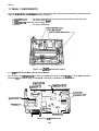
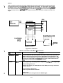
1.7 MAIN COMPONENTS
The main mmponents of the LQ-570+ printer are designed for easy removal and replacement at maintenance and
repair of the printer. The main composed of this printer are:
the main control board; the CPU on this board controls all main functions.
1) C107 MAIN board:
the control panel bowd.
2) C062 PNL board:
3) C062 PSWPSE board: the power supply board.
4) M-5J1O:
the printer mechanism.
Figure 1-11. LQ-570+ Component Layout
1.7.1 C107 MAIN Board (Main Control Circuit Board)
This consists of a TMP90C041N 6-bit CPU, an E05A50 gate array, a PROM (512K), a mask ROM (character
generator, 2M), Head Gate Array, an EEPROM, a CR Driver, a PF Driver and Head Drivers.
STK6712(!C1O)
E05A50(IC11)
\
\
CPU TMP90C041(IC21)
I
“ MASKROM(IC17)
PROM(IC1 4),
-UJ
o
I
w-
1
I
Eo5A6k(lc2)
Figure 1-12. C107 MAIN Board
1-26
o
REV.-A
(
1.7.2 C062 PNL Board (Control Panel Circuit Board)
The C062 PNL board is the LQ-570+ control panel, which includes the indicator LEDs, switches, and DIP switches.
Figure 1-13. (X62 PNL Board
1.7.3 C062 PSB/PSE Board (Power Supply Circuit Board)
The power supply unit consists of a switching regulator circuit, which mnverts the AC line vottage to the DC voltages
(for example, +35V and +5V) used by the printer. The C062 PSB board is 120V input type, and the C062 PSE board
is 220/240V input type.
Figure 1-14. C062 PSB/PSE Board
1-27
REV.-A
~
1.7.4 Printer Meohanism (M-5J1O)
The M-5J1o printer mechanism was developed specifically for use with LQ-570+ printer. The components inciude
a carriige motor, carriage mechanism, paper-feed motor, paper-feed mechanism, ribbon-feed mechanism, printhead,
and sensors. This printer mechanism ailows three ways of paper insertion.
/“
Figure 1-15. Modei-6J10 Printer Mechanism
1.7.5 Housing
The LQ-570+ housing consists of the upper, lower, and front cases. The front case houses the contmi panel board.
The lower case holds the printer mechanism, the main controi circuit board, and power supply circuit board.
,
v
Figure 1-16. Housing
1-28
I
CHAPTER 2
OPERATION PRINCIPLES
2.1 OVERVIEW OF PRINTER MECHANISM OPERATION . . . . . . . . . . . . . . . . . . . . . . . . . 2-1
2.1.1 Printhead Mechanism . . . . . . . . . . . . . . . . . . . . . . . . . . . . . . . . . . . . . . . . . . . . . . 2-1
2.3 CONTROL CIRCUIT OPERATION . . . . . . . . . . . . . . . . . . . . . . . . . . . . . . . . . . . . . . 2-13
2.3.1 Control Cirouit Operation Overview . . . . . . . . . . . . . . . . . . . . . . . . . . . . . . . . . . 2-13
2.3.2 Reset Cirouit . . . . . . . . . . . . . . . . . . . . . . . . . . . . . . . . . . . . . . . . . . . . . . . . . . . . 2-15
2.3.3 Sensor Cirouits . . . . . . . . . . . . . . . . . . . . . . . . . . . . . . . . . . . . . . . . . . . . . . . . . . 2-16
2.3.4 MOTOR, CR Drive Circuit . . . . . . . . . . . . . . . . . . . . . . . . . . . . . . . . . . . . . . . . . . 2-17
2.3.5 MOTOR, PF Drive Cirouit . . . . . . . . . . . . . . . . . . . . . . . . . . . . . . . . . . . . . . . . . . 2-18
2.3.6 Printhead Drive Circuit . . . . . . . . . . . . . . . . . . . . . . . . . . . . . . . . . . . . . . . . . . . . 2-19
i
’
LIST OF FIGURES
Figure 2-1. How the Printhead Works . . . . . . . . . . . . . . . . . . . . . . . . . . . . . . . . . . . . . . . .
Figure 2-17. Control Circuit Blook Diagram . . . . . . . . . . . . . . . . . . . . . . . . . . . . . . . . . . .
Figure 2-18. Data Flow . . . . . . . . . . . . . . . . . . . . . . . . . . . . . . . . . . . . . . . . . . . . . . . . . .
Figure 2-19. Reset Circuit Blook Diagram . . . . . . . . . . . . . . . . . . . . . . . . . . . . . . . . . . . .
Figure 2-20. /RESET Signal Timing . . . . . . . . . . . . . . . . . . . . . . . . . . . . . . . . . . . . . . . . .
Figure 2-21. Sensor Ci&dt Block-Diagram . . . . . . . . . . . . . . . . . . . . . . . . . . . . . . . . . . .
Figure 2-22. MOTOR, CR Drive Circuit . . . . . . . . . . . . . . . . . . . . . . . . . . . . . . . . . . . . . .
Figure 2-23. MOTOR, PF Drive Circuit . . . . . . . . . . . . . . . . . . . . . . . . . . . . . . . . . . . . . . .
Figure 2-24. Printhaad Drive Cirouit . . . . . . . . . . . . . . . . . . . . . . . . . . . . . . . . . . . . . . . .
2-1
2-13
2-14
2-15
2-16
2-16
2-17
2-18
2-19
LIST OF TABLES
Table 2-5. Funotions of the Main IC and Circuits . . . . . . . . . . . . . . . . . . . . . . . . . . . . . .
Table 2-6. MOTOR, CR Drive Modes . . . . . . . . . . . . . . . . . . . . . . . . . . . . . . . . . . . . . . . .
1
i,
2-i
I
2-14
2-17
REV.-A
{(
2.1 OVERVIEW OF PRINTER MECHANISM OPERATION
This section describes the printer mechanism of the Model-5J10 printer unit and explains how the printer works.
Model-5J10 has a printer mechanism that features a 24-pin impa~ dot printhead for serial printing. There are four
main parts to the printer mechanism: 1) the printhead mechanism, 2) the carriage movement mechanism, 3) the
paper advance mechanism, and 4) the ribbon advance mechanism. Each of these is described below.
2.1.1 Printhead Mechanism
The printhead mechanism consists of the printhead itself, the ink ribbon, and the platen. The printhead mntains 24
wires in a zigzag arrangement in two rows of 12. A drive coil is provided for each of these wires to make the wires
move in and out of the printhead and print dots independently of each other. The basic way that the wires are driven
is described in the four steps below.
1.
2.
3.
4.
The control circuit outputs the drive signal to the printhead drive circuit. This changes the printhead drive
voltage, and current flows through the corresponding pnnthead coil. The coil acts as a solenoid and generates
a magnetic force.
This induced force causes the plate to approach the coil md and the associated dot wire is rapidly ejected to
impact on the platen.
The dot wire presses the ink ribbon up against the paper as it hits the platen, and in this way prints a dot on
the paper.
As soon as the current through the coil is switched off, the force induced in the mil rod stops. The plate then
returns to its original position-(its position before the coil was energized) through the action “of the p~te spring.
After the dot wire hits the platen, the rebounding force of hitting the platen works together with the wire return
spring to pull the wire back to its original position in relation to the plate.
PLATEN
RIBBON MASK
Oot Wire
/
Wtm Reaetti~g Spring
/
\
Stopper
\
/
\
/
Ribbon
/
Pa&r
Act&ing Plate Spring
+
Figure 2-1. How the Printhead Works
Figure 2-1 shows the action of the printer mechanism when a single dot is printed.
The printhead tends to heat up aftera period of mntinuous printing. To minimize the possibility of the dot wire drive
coils overheating within the printhead and any loss of performance, the head is equipped with a thermistor that
detects the head temperature. When this thermistor detects changes intheprinthead temperature, thevoltagesignal
changes. This signal change is read by the control circuit for feedback mntrol.
2-1
REV.-A
f
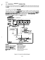
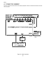
2.3 CONTROL CIRCUIT OPERATION
The control circuit consists of two boards: the C107 MAIN board, which acts as the main board, and
the C062 PNL board, which acts as the control panel board. This section describes how these boards
work.
2.3.1 Control Circuit Operation Ovewiew
The printer CPU is an 8-bit CPU TMP90C041 running at 10 MHz. It oversees control of all the
components of the printer. The E05A50 gate array contains various memory management ftinctions
that control the assignment of the memoty and l/O areas, and it controls a head gate array IC2
(E05A86), a PU1501 or STK-67129 for the PF and CR motor driver, STA475A(IC4 - IC9) is transistor
array for the head pins drive, several sensor circuits and so on.
Figure 2-17 shows the block diagram of the C107 Main Board.
C062PNL Board
Card Panel
I
C107MAIN Board
-..
-.. —.. —..
~
, -1----”:”--------—— . . . . . . . . . . . . . . . . . .
. . . . . . . . . .,
: Opdon I/F } . .
...........
GateArray
E05A50
(Icll)
PROM
512K
(IC14)
P:5s
psM~M
MROM
MROM
(IC15)
(IC16)
(I%)
(lfi8)
I
I
Vref Circuit
I
i
a
I
CPU TMP90C041 (IC21)
LSTK-6712(IC1O)
I
1
I
I
L’
E05A66 (IC2)
STA47SA (IWIC9)
+
CR Motor
I
%F
(
Prfnthaad
:- ” - ” - - - :
; 1+~
‘~.
I
“. . . . . . . . .
PFMotor
+
DETECTOR ASSY.,
HP
v
D~~OR
ASSY.,PE,REAR
1
v
DmcroR ASSY.,
RELEASE
DETECTOR
D151ECTOR ASSY.,
ASSY.,PE,FRONT PLATEN
Head
Thermiater
Sanaor
CR Motor
PF Motor
DETECTOR ASSY.,PE,FRONT
DETECTOR ASSY.,PE,REAR
DETECTOR ASSY.,HP
DETECTOR ASSY.,PLATEN
DETECTOR ASSY.,RELEASE
TH2
: Carriage Motor
: Paper Feed Motor
: Paper End Sensor(Front)
: Paper End Sensor(Rear)
: Home Position Sensor
: Platen Gap Sensor
: Release Lever Position Sensor
: Therrnister Sensor
Figure 2-17. Control Circuit Block Diagram
2-13
REV.-A
‘)
Table 2-5 lists the functions of the main components and circuits of the printer. The CPU converts the
print data sent from the host mmputer to image data (the print image). The image data is then loaded
to RAM. Each line of data is processed sequentially. The CPU transfera the print data to the printhead
drive circuit. The CPU sends the printhead drive pulse to the printhead drive circuit. The length of this
pulse corresponds to the printhead drive voltage. The head drive circuit then outputs the head drive
signal.
RAM
CPU(IC21)
Input
Buffer
I
Print Data
C6nvertor
- - - - - Image
Buffer
Image Data
Transfer
G/A E05A86
(IC2)
m
‘=-’”)
Date Latch and
Delay control
Printhrad
Figure 2-18. Data Flow
‘)
Table 2-5. Functions of the Main IC and Circuits
IC or Circuit
Functions
Location
TMP90C041
IC21
Receives data from the host computer and loads the data to the input buffer in
RAM (under interrupt processing control). Expands the input data held in the
buffer to create image data. Loads this image data to the image buffer in RAM.
Transfers the image data to the printhead drive circuit. It also controls various
pwts of the printer mechanism, such as the motors.
E05A50
Icll
This is a gate array consisting of three components mnfigurd on a single chip:
Memory Management Unit
Handles CPU memory in ROM, RAM, and mask ROM, and assigns addresses
for other devices.
Parallel Interface (Parallel I/F)
Holds the parallel interface functions.
‘}
Reset Circuit
Contains the circuit that generates the /RESET signal.
2-14
REV.-A
Table 2-5. Functions of the Main IC and Circuits (Cont.)
Functions
IC or Circuit
Location
PROM
IC14
PROM contains the program that runs the CPU.
RAM
IC15
IC16
Holds the CPU working area and the various buffers. (1E is not used for an 80column device and is not installed.)
MROM
(Mask ROM)
IC17
IC18
Holds the character design (also called the character generator).
EEPROM
IC12
EEPROM is an electronically writable and erasable ROM used to hold such
information as the TOF position.
HEAD GATE
ARRAY
IC2
This is a gate array mnsisting of three components configured on a single chip:
s Change order of the Head pulse outputs
Mode 1: HD1+HD2+HD3+......+HD22+HD23+HD24
Mode 2: HD24+HD23+HD22+...... +HD3+HD2+HD1
● Delay control(for low noise)
● Image data latching
Vref Circuit
...
This is a circuit for generating the reference voltage used in the A/D mnvertor
within the CPU.
2.3.2 Reset Circuit
Figure 2-19 shows the reset circuit block diagram. The reset circuit issues the /RESET signal. Each
part of the control cimuits is initialized when this /RESET signal is received. The renditions when the
/RESET signal is output are described below.
When Turning on the Power Supply
Immediately after the power has been turned on, PST 529 (IC19) outputs the /PON pulse. E05A50
(IC1l) receives this pulse and then outputs the /DISC pulse. The electrical charge in the
capacitor(C29) is then discharged. After this, The /THLD port within E05A50 detects the low level and
then outputs the /RESET signal from the /OUT port of IC19. After a certain time has elapsed, the
charge in the condenser builds up again. The M-ILD signal is canceled and then the /RESET signal
is canceled.
Resets performed by the CPU itself (CPU self-reset)
The CPU outputs the /RESET signal if there is a /RESET request for E05A50 and E05A50 output the
/DISC pulse. ”
E05A50(IC11)
I
$ R30
a,
107
IOUT
/PON
/THLD
ZC”fi IDISC
I
+5
1C2’1
~z,
I
R32”
-rl-
7+7+
Figure 2-19. Reset Circuit Block Diagram
2-15
REV.-A
Power On
CpU Self Reset
t
4
+6 V Line
VCCOM
I
I
u
THLD
??EStt
Figure 2-20. /F?ESET Signal Timing
2.3.3 Sensor Circuits
Figure 2-21 shows thesensorcircuits block diagram. Detection of any excessive printheadtemperature
causes the TEMP2 signal to be sent directly to the CPU. Other signals, such as the CRHOME signal,
pass through the each low path filters before reaching the CPU. Terminals P50 to P55 on the CPU
are used for the ND mnvertor. The Vref circuit generates the A/D mnverior reference voltage Vref.
Printhead
I T M P 2 11
I
- - - - - - - - - - - - - - - - - - - - - - - - - - - - - - - - - - - - - - - - - - -
,: Sensor Circuit
+5
4
,,
6.2K
‘‘1
‘
t
k
I
a
1
)
LEVER
GAP
‘E-1
,
~’~n.
dvk
LEVER
3
GAP
--- . - - - --- --PE-1
PE-2
Vref Circuit
CRHOME, %’:
.--------------,
L
‘:
‘
:
-. . . . . . . .
=“”’
0.022 ;
T
777-;
- - - - - - - - - - - - - --1
r
Head Drive Voltage
(+35V) monitor Circuit
Figure 2-21. Sensor Circuit Block Diagram
2-16
.
CPU(IC21
P50
D
P31
P34
D
P52
P53
P54
VREF
:
4
D
P51
REV.-A
2.3.4 MOTOR, CR Drive Circuit
Figure 2-22 shows the MOTOR, CR driie circuit. An open-loop, constant-current drive control is used
to drive the MOTOR, CR. The motor is driven by 2-2 phase excitation and 1-2 phase excitation. 2-2
phase excitation corresponds to two 1-2 phase excitation steps. Thus, for each single step phase
change of a 2-2 phase excitation motor, the carriage moves 1/120 inch. For each single step phase
change of a 1-2 phase excitation motor, the carriage moves 1/240 inch.
The MOTOR, CR driie circuit of the STK-67128 detects the amount of current flow in the MOTOR, CR
coil and regulates it. The current flowing through the coil varies depending on the speed of the
MOTOR, CR.
The amount of current is set by the CPU via the E05A50 l/O port. Signals are sent to Vrefl or Vref2
on the STK-67128. The STK-67128 sets the coil current to mnespond to the MOTOR, CR speed.
Ports P60 to P63 on the CPU are used exclusively as phase control potts for the stepping motor.
-. ---- -- . .
(IC21)
MOTOR,CR
STK-6712
P60
P61
P62
P63
-
E05A50
-1=3
I
Current
Control
Circuit
Al
BI
IAI %l=s-=~~:;
/B1
/Ad
IB4
VREFA
:
.--..--.---.-
VREFB
k
Figure 2-22. MOTOR, CR Drive Circuit
Tshla
----- Mnchs
------. ---- 7-I%
- -. MOTOR.
... - . -. ., CR
-. . Driva
Drive Mode
)
Extension Type
Type Drive Frequency
3 x speed
2-2 phase
2695
2 x speed
1.5 x speed
4/3 x speed
1 x speed
3/4 x speed
2/3 x speed
1/2 x speed
2-2 phase
2-2 phase
1-2 phase
1-2 phase
1-2 phase
1-2 phase
1-2 phase
1773 pps
1347 pps
1191 pps
1796 P@
1347 pps
1190 pps
898 PPS
1
PPS
2-17
Standard Print Character
Draft
High Speed LQ
Draft(Emphasis, Condensed)
LQ
REV.-A
“)
2.3.5 MOTOR, PF Drive Circuit
The printer uses a stepping motor to advance the paper. The paper can be advanced for minimum of
1/380 inch. The nmtor is a 2-2 phase or 1-2 phase, constant-voltage drive type. P70 to P73 on the
CPU are the phase oontml ports forthe stepping motor. MOTOR, PF phase data output through these
ports. Cl to C4 are turned on and off within the PU1501(IC3) acoording to the phase data sent from
the CPU.
When the paper advanoe motor is running, the supply voltage to the mil of the MOTOR,PF is +35 V.
When the paper advance motor is not running and is in hold state, the supply voltage to the coil is +5
V. Switching between these two supply voltages oocursat the CPterminal of the PU1501(IC3) when
the switch is turned on or off.
pu,~(),
TMP90C041
(IC21)
,
:
(IC3)
B1
B2
03
04
P70
P71
P72
P73
-- MOTOR,PF
.
---------,
cl
C2
C3
C4
:
:
‘
➤
PFA
PF-A
PFB
:
PF-B :
E05A50
(Icll)
Data
Bus
P3
BP
A,
CP
r
‘)
Figure 2-23. MOTOR, PF Drive Circuit
2-18
db
REV.-A
‘\
2.3.6 Printhead Drive Circuit
Figure 2-24 shows the printhead drive circuit block diagram. The print data already is expanded to
create the image data. The CPU splits up this data three times and transfers this information to the
latch circuit within the Head Gate Array(lC2). The CPU samples the voltage of the +35 V line via the
A/D convertor (see Section 2.3.3). The CPU outputs a pulse via the CPU time output pori P63. The
length of this pulse corresponds to the voftage of the +35 V line. This pulse becomes the head drive
signal. In this way, Head Gate Array(iC2) outputs head drive signals (signals HD1 to HD24) that relate
to voltage level through the width of the pulses. These signals are output to the head for each of the
section of print data that were created by subdividing the data three times before sending.
By sampling the +35 V line voltage and determining the length of the head drive signal, it is possible
to maintain the energy supplied to the head at a mnstant level. If the voltage of the +35 V line is .
HIGH, the CPU shortens the output pulse. If the voftage of the +35 V line is LOW, the CPU lengthen
the output pulse.
TMP90C041
(IC21)
DO -D7
E05A86
STA475
(IC2)
(IC4-9)
DO -D7
E05A50(IC11)
HD1 -24
‘“npp ‘Pp”rrs
Figure 2-24. Printhead Drive Circuit
2-19
Printhead
REV.-A
‘)
CHAPTER 3
DISASSEMBLY AND ASSEMBLY
3.2.1 Changing the Printhead . . . . . . . . . . . . . . . . . . . . . . . . . . . . . . . . . . . . . . . . . . . . .
3.2.3 Removing the Eleotrkal Cirouitty . . . . . . . . . . . . . . . . . . . . . . . . . . . . . . . . . . . . .
3.2.3.1 Removing the BOARD ASSY.,MAIN (C107 MAIN Board) . . . . . . . . . . . . . . . . .
3.2.3Q Removing the BOARD ASSY.,POWER SUPPLY (C062 PSWPSE Boami) . . . . .
3.2.3.3 Removing the BOARD ASSY.,PANEL (C062 PNL Board) . . . . . . . . . . . . . . . . .
3-5
3-7
3-7
3-3
3-3
LIST OF FIGURES
)
Figure 3-2. Removing the Printer Cover and the Paper Eject Cover . . . . . . . . . . . . . . . . . 345
Figure 3-3. Removing the Printhead
. . . . . . . . . . . . . . . . . . . . . . . . . . . . . . . . . . . . . . . . . 3-s
Figure 3-6. Removing the Shield Plate . . . . . . . . . . . . . . . . . . . . . . . . . . . . . . . . . . . . . . . 3-7
Figure 3-7. Removing the BOARD ASSY.,MAIN . . . . . . . . . . . . . . . . . . . . . . . . . . . . . . . . . 3-7
Figure 3-S. Removing the BOARD ASSY.,POWER SUPPLY . . . . . . . . . . . . . . . . . . . . . . . . 3-3
Figure 3-9. Removing the BOARD ASSY.,PANEL . . . . . . . . . . . . . . . . . . . . . . . . . . . . . . . 3-s
3-i
REV.-A
3.2.1 Removing the Circuit Boards
)
1.
2.
Remove the FRAME ASSY.,SHEET GUIDE.
Remove the COVER ASSY.,EJECT.
COVERASSY.,EJECT
ASSY.,SHE= GUIDE
Figure 3-2. Removing the FRAME ASSY., ;HEET GUIDE and the COVER ASSY., EJECT
3.
4.
Release the two levers that hold the printhead to the oarriage, and remove the printhead.
Remove the two FFCS (CABLE, HEAD, FRONT(,REAR)) from the printhead.
prifIthead
Figure 3-3. Remove the Printhead
3-5
REV.-A
3.2.3 Removing the Circuit Boards
)
This section describes how to remove the BOARD ASSY.,MAIN (C107 MAIN board), the BOARD
ASSY.,POWER SUPPLY (C062 PSB/PSE board) and the BOARD ASSY.,PANEL (C062 PNL board).
3.2.3.1 Removing the BOARD ASSY.,MAIN (C107 MAIN Board)
1.
2.
3.
4.
Remove the HOUSING ASSY.,UPPER (see Section 3.2.2.2).
Remove the CB (M3 X 6) screw that hold the HOLDING PLATE,FFC to the SHIELD PLATE,MAIN
BOARD, and remove it.
Disoonneot the FFC(CABLE,HEAD, FRONT(REAR)) removing the oables for the CN6 and CN7
mnneotors on the BOARD ASSY.,MAIN.
Remove three CBB (C) (M3 X 10) sorews that hold the SHIELD PLATE,MAIN
BOARD to the BOARD ASSY.,MAIN, and remove it.
[
CBB(C) (M4x 14) Screw
SHIELD PLATE, RIGHT>
cCB (M3X6) Screw
C!
lliE%&2-
CBB (M4X 10) Screw -
~
MAIN
BOARD
/
BOARD ASSY., MAIN CBB(C) (M3X 10) Screws
Figure 3-6. Removing the Shield Plate, MAIN BOARD
)
5.
Remove the CBB (M4 X 10) sorew that hold the SHIELD PLATE, RIGHT to the BOARD
ASSY.,MAIN. Remove the CBB(C)(M4 X 14) screws that hold it to the
HOUSING ASSY.,LOWER. Remove the SHIELD PLATE, RIGHT.
6.
Remove the cables from the following connectors on the main board: CN3 (brown 12-pin), CN4
(white 5-pin), CN5 (white 6-pin), CN8 (yellow 2-pin), CN9 (black 2-pin), CN1O (blue 2-pin),CN11
(white 2-pin) and CN12 (red 2-pin).
Remove three CBB(C) (M3 X 10) screws and CB A-IAMITITE (M3 X 8) sorew that hold the h
board to the lower ~sej Remove the main board.
7.
CAUTION
Be oareful with a color of the harness cable when you connect them to the mnnector CN1l and
CN12 of the Main board. The connect connection should be as below.
Hamess(BLACK)+CNl 1(WHITE)
Hamess(GRAY)+CN12(WHlTE)
3-7
REV.-A
CBB(C) (M3X 10) Screws
CB (M3X8)’Screw BOARD ASSY., MAIN
Figure 3-7. BOARD ASSY.,MAIN
Adjustment Required
When replacing the BOARD ASSY.,MAIN, you must adjust the bidirectional print position again
to ensure bidirectional printing is mrrectly aligned
<Bidirectional Print position adjustment(See section 4.2)>
3.2.3,2 Removing the BOARD ASSY.,POWER SUPPLY (C082 PSB/PSE Board)
1.
2.
3.
4.
Remove the HOUSING ASSY.,UPPER (see Section 3.2.2.2).
Remove the cable from the connector CN13 of the BOARD ASSY.,MAIN.
Remove the cable for connector CN1 of the BOARD ASSY.,POWER SUPPLY.
Remove five CBB(C) (M3 X 10) screws and the CB (M3 X 8) screw that hold the BOARD
ASSY.,POWER SUPPLY to the HOUSING ASSY.,LOWER. Remove the BOARD ASSY.,
BOARO ASSY., POWER SUPPLY (C062 PSB/PSE 60sd)
POWER SUPPLY.
)
CBS(C) (M3 X 10) Screws
Figure 3-B. Removing the BOARD ASSY.,POWER SUPPLY
3.2.3.3 Removing the BOARD ASSY.,PANEL(C082 PNL Board)
1. Remove the HOUSING, FRONT (see Section 3.2.2.1).
2. Remove five CBB(C) (M3 X 10) screws that hold the BOARD ASSY.,PANEL to the
HOUSING, FRONT. Remove the BOARD ASSY.,PANEL.
Figure 3-9. Removing the BOARD ASSY.,PANEL
3-8
“’)
CHAPTER 4
ADJUSTMENTS
4.3 CIRCUIT ADJUSTMENT . . . . . . . . . . . . . . . . . . . . . . . . . . . . . . . . . . . . . . . . . . . . . . . . . . . . . . . . .
4.3.1 Adjustment Process . . . . . . . . . . . . . . . . . . . . . . . . . . . . . . . . . . . . . . . . . . . . . . . . . . . . . . . .
4-i
4-6
4-3
REV.-A
‘) 4.3 CIRCUIT ADJUSTMENT
The C107 MAIN board contains variable resistor VR1, which is used for balancing the circuitry. When any of the
following parts are replaced, the circuitry must be balanced by adjusting the VR1.
R6, R7, TL431(IC1), and VR1
If the circuitry is not properly adjusted, the CPU A/D converter functions abnormally and causes irregular operation
of the printer.
4.3.1 Adjustment Process
Attach a digital multimeter to the check terminal TP1 (Vref voltage) on the C107 MAIN board. Turn the printer On
and adjust the variable resistor VR1 until a reading of 4.741 V is obtained.
4-6
CHAPTER 5
TROUBLESHOOTING
)
BY UNIT REPLACEMENT . . . . . . . . . . . . . . . . . . . . . . . . . . . . . . . . . . . . . . . . . . . . . . . . 5-8
5.4 REPAIR OF THE MAIN BOARD . . . . . . . . . . . . . . . . . . . . . . . . . . . . . . . . . . . . . . . . . . . . . . . . . . 5-14
5.5 REPAIR OF THE PRINTER MECHANISM . . . . . . . . . . . . . . . . . . . . . . . . . . . . . . . . . . . . . . . . . . . 5-17
5.2 REPAIR
LIST OF FIGURES
Figure S2. Printhead Resistance . . . . . . . . . . . . . . . . . . . . . . . . . . . . . . . . . . . . . . . . . . . . . . . . . . . .
5-s
LIST OF TABLES
Table
Table
Table
Table
‘)
5-2. Error Displays . . . . . . . . . . . . . . . . . . . . . . . . . . . . . . . . . . . . . . . . . . . . . . . . . . . . . . . . . . $1
5-3. Symptoms and Referenoe Pages . . . . . . . . . . . . . . . . . . . . . . . . . . . . . . . . . . . . . . . . . . . 5-2
S5. Repair of the Main Circuit Board . . . . . . . . . . . . . . . . . . . . . . . . . . . . . . . . . . . . . . . . . . . 5-14
5-6. Repair of the Printer Meohanism . . . . . . . . . . . . . . . . . . . . . . . . . . . . . . . . . . . . . . . . . . . 5-17
\
REV.-A
0
o #3
o #5
o #7
o #9
o #11
o *13
o
o
o
o it21
o 423
#1
# 2 0
# 4 0
N60
# 8 0
o
0
0
0
0
0
0
H 240
(
86 410 418
#122
‘-
*7
82 83
#17
H19
Wire Assignment
Coil Resistance:
45.5 *3.2 fl at 25*C
(Between each dot wire and common.]
( Terminal Assignment J
Figure 5-2. Printhead Resistance
5-8
#15
REV.-A
)
5.3 REPAIR OF THE MAIN BOARD
This section provides instructions for repairing the main board when it is defective and describes variius symptoms,
likely causes, and checkpoints. Checkpoints refer to proper waveforms, resistance values, and other values to be
checked to evaluate the operation of any component that might be bad. Check these values and take the
appropriate action.
Table 5-4. Re~air of the Main Circuit Board
)
“)
‘)/
5-14
‘)
Tabla
the .-.Main
Circuit—-—Board
----- 5-4.
- . . .Ranair
.- .1- . . nf
-. ---—... ------— ,—(Continued
—-----–—. . . .
‘)
)
)
5-15
REV.-A
‘?
Table
of the Main Circuit Board (Continued)
—— =. Rebair
.
—r——
Problem
Symptom
Cause
Checkpoint
The carnage
operates
abnormally
Carnage
operation Is
unstable(lack
of torque)
Iclo Is
defectrve
Self-test
prmtmg IS
abnormal
Self-test w not
executed
The CPU can
not measure
the voltage on
the +35V hne
Measure the voltage at pm 59(Vref) of
IC21 The normal voltage IS 4741 V
Icll
At IC11, check the input signal at pm
101 and the output signal at pm 46
Is
defective
Solutlon
Replace
Iclo
Adjust VR1
(Refer to
43)
Replace
IC4D
‘)
A particular
dot IS not
being printed
IC4 - IC9 Is
defecttve
For example, check the output signal at
pm2 and the out put signal at pm3 wtth
IC4
Replace IC4
- IC9
The paper
does not feed,
or the feed
pnch IS
abnormal
IC3 Is
defectwe
Check the input signal at pml and the
output signal at pm2
Replace IC3
)
Paper Is not
led normally
)
5-16
REV.-A
‘)
5.5 REPAIR OF THE PRINTER
For detailed procedures for replacing or adjusting parts, refer to Chapter 3, Dimssemb/yandAswmb/y, and Chapter
4, Ao@hr?ent. If a problem or symptom recurs following an attempted repair, refer to Table 5-5 to try to find other
potential causes.
Table -. ReDair
of the Printer Mechanism
.
Problem
‘)
Symptom
Cauae
Checkpoint
Solution
The carriage
The carriage motor
Foreign substances
Manually move the
motor fails to
operate.
completely fails to
activate at power
on.
are lodged in the
gears or elsewhere
in the mechanism.
timing belt to see if
this causes the motor
to rotate.
The carriage motor
is defective.
Measure the coil
resistance of the
motor. The
resistance should be
about 19.5 ohms.
Replace the
carriage motor.
The belt pulley is
defective.
Check for broken or
worn pulley.
Replace the belt
pulley.
The timing belt is
defective.
Check that the timing
belt is correctly
inserted into the
bottom of the
carriage.
Reinsett the
timing bett.
Check for a broken
timing belt.
Replace the
timing belt.
The carriage does
not operate at
power on (after
the carriage has
been manually
centered prior to
power on.)
‘)
Self-test printing
does not execute.
The carriage motor
rotates, but the
carriage does not
mwe.
Remove any
foreign
substances.
The carriage
moves left slightly,
then stops.
Carriage movement
is not smooth.
Check whether the
carriage moves
smoothly when
moved manually.
Clean and
lubricate.
The carriage
moves to the left or
right end, then
stops.
The home position
sensor is defective.
Use a multimeter to
check the home
position sensor.
Replace the home
position sensor.
The carriage
moves, but no
printing is
performed.
The printhead FFC
common wires are
disconnected.
Check the common
wires for the
printhead FFC.
Replace the FFC.
5-17
REV.-A
)
Tahln
. . . . . . . . . . . . . .(Continued}
. .\. --..-..--——,
. ---- -K
. -.Rannir
. .- ~-..nf-.tha
. . . Printar
. . . . . . . Maehanism
Problem
Self-test printing
is abnormal.
Symptom
A particular dot
fails to print.
The printing is too
light, or the print
density is not
uniform.
Cause
Printing is
petiormed, but the
paper is not fed, or
is not fed uniformly.
Solution
Measure the coil
resistance of the
printhead. The
normal value is
approximately 45.5
ohms.
Replace the
printhead.
Check whether the
dot wire is worn.
Replace the
printhead.
The printhead is
defective.
Check whether the tip
of the dot wire is
worn.
Replace the
printhead.
The platen gap is
not properly
adjusted.
Set the gap adjust
lever to the second
position, and check
the gap between the
tip of the printhead
and the platen.
The appropriate
value is 0.48 mm.
Adjust the gap.
Refer to Section
4.1.2, Platen Gap
A@stment.
Foreign substances
are lodged in the
paper path.
Petform a visual
check of the paper
path.
Remove any
foreign
substances.
The paper-feed
motor is not driving
the gear correctty.
Check that no foreign
substance is lodged
between the gears,
and that the gears
are not broken or
worn.
● Remove any
foreign substance.
● Repface the
paper-feed
reduction gear.
● Replace the
platen gear.
The paper-feed
motor is defective.
Measure the mil
resistance for the
paper feed motor.
The approximate
value should be 79
ohms.
Replace the
paper-feed motor.
The printhead is
defective.
“’l
Paper feeding is
abnormal.
Checkpoint
‘.,
5-18
.
REV.-A
TsIhla
Mechanism
, . . . ,
—-- —.. .— --- (Continued)
. ---- 5-!5.
- -- Ranair
------- nf
-- Printer
- ------- ----
‘1
Problem
The ribbon feed is
abnormal.
‘)
Paper becomes
stained.
Printing mntinues
after the paper
ends or when no
paper is loaded.
Symptom
Cause
Checkpoint
Solution
The ribbon
cartridge is
defective.
Dismount the ribbon
cartridge, rotate its
knob manually, and
check whether the
ribbon feeds
normally.
Replace the
ribbon cartridge.
Foreign substances
are caught in the
gears.
Check whether the
ribbon driving gear
rotates when the
carriage is moved
manualty.
● Remove any
foreign substance.
● Replace
the .
ribbon-feed
mechanism.
The ribbon feeds
properly only when
the carriage moves
in one direction
(i.e., it fails to feed
when the cam.age
moves in the other
direction).
The planetaty lever
is defective.
Move the carriage
manually, and check
whether the planetary
lever turns in reverse
and engages the
gear.
Replace the
tibbon-feed
mechanism.
Ink stains appear
on areas where
there is printing.
The ribbon mask is
not mrrectly
positioned.
Check whether the
ribbon mask .S in the
correct position.
Reinstall the
n!bbon mask.
The platen gap is
not adjusted.
Set the gap adjust
lever to the second
position, and check
the gap between the
tip of the printhead
and the platen.
The appropriate
value is 0.46 mm.
Adjust the gap.
Refer to Section
4.1.2 P/aten Gap
A@stment.
The paper-end
sensor is defective.
Check the paper-end
sensor switch.
Replace
the
~
paper-end sensor. ~•••y;n•
The ribbon is not
fed.
Printing continues
past the paper end.
5-19
REV.-A
APPENDIX
Al CONNECTOR SUMMARY . . . . . . . . . . . . . . . . . . . . . . . . . . . . . . .
A.2 CIRCUIT DIAGRAMS . . . . . . . . . . . . . . . . . . . . . . . . . . . . . . . . . .
A.3 CIRCUIT BOARD COMPONENT LAYOUT . . . . . . . . . . . . . . . . . . .
A.4 EXPLODED DIAGRAM . . . . . . . . . . . . . . . . . . . . . . . . . . . . . . . . .
A.5 CASE OUTLINE DRAWING . . . . . . . . . . . . . . . . . . . . . . . . . . . . . .
A-1
. . . . . . . . . . . . . . . . . . . . . . . . A-5
A-12
......................
. . . . . . . . . . . . . . . . . . . . . . . A-16
. . . . . . . . . . . . . . . . . . . . . . . A-22
........................
LIST OF FIGURES
Figure A-1. Cable Connection . . . . . . . . . . . . . . . . . . . . . . . . . . . . . . . . . . . . . . . . . . . . . . . . . . . . . .
Figure A-3. BOOARD ASSY.,MAIN(C107 MAIN BOARD) . . . . . . . . . . .
Figure A-9. BOARD ASSY.,MAIN Component Layout . . . . . . . . . . . . .
Figure A-13. LQ-570+ Exploded Diagram . . . . . . . . . . . . . . . . . . . . . .
Figure A-15. Model-5J10 Exploded Diagram . . . . . . . . . . . . . . . . . . . .
. Figure A-17. LQ-570+ Case Outline Drawing . . . . . . . . . . . . . . . . . . . .
........................
.......................
.......................
.......................
. . . . . . . . . . . . . .’. . . . . . . . .
A-1
A-6
A-12
A-16
A-18
A-22
LIST OF TABLES
.. .. .. .. .. .. .. .. .. .. .. .. .. .. .. .. .. .. .. .. .. .. .. .. :2
.. .. .. .. .. .. .. .. .. .. .. .. .. .. .. .. .. .. .. .. .. .. .. .. :
... .. . .. ... ... ... .. . .. . .. ... ... . . . .
Table A-1. Board Corm-or Summary . . . . . . . . . . . . . . . . . . . . . . . . . . . . . . . . . . . . . . . . . . . . . . . . Table A-2. CN2 BOARD ASSY.,MAIN(C107 MAIN) . . . . . . . . . . . . . . . . . . . . . . . . . . . . . . . . . . . . . . . .
A-3
Table A-3. CN3 BOARD ASSY.,MAIN(C107 MAIN) . . . . . . . . . . . . . . . .
Table A+. CN4 BOARD ASSY.,MAIN(C107 MAIN) . . . . . . . . . . . . . . . .
Table A-5. CN5 BOARD ASSY.,MAIN(C107 MAIN) . . . . . . . . . . . . . . . .
A-3
Table A-6. CN6 BOARD ASSY.,MAIN(C107 MAIN) . . . . . . . . . . . . . . . .
Table A-7. CN7 BOARD ASSY.,MAIN(C107 MAIN) . . . . . . . . . . . . . . . .
.’. . . . . . . . . . . . ::
Table A-8. CN8 BOARD ASSY.,MAIN(C107 MAIN) . . . . . . . . . . . . . . . .
Table A-9. CN9 BOARD ASSY.,MAIN(C107 MAIN) . . . . . . . . . . . . . . . . . . . . . . . . . . . . . . . . . . . . . . . . A-4
Table A-10. CN1O BOARD ASSY.,MAIN(C107 MAIN) . . . . . . . . . . . . . . . . . . . . . . . . . . . . . . . . . . . . . .
Table A-n. CN1l BOARD ASSY.,MAIN(C107 MAIN) . . . . . . . . . . . . . . . . . . . . . . . . . . . . . . . . . . . . . . ::
Table A-12. CN12 BOARD ASSY.,MAIN(C107 MAIN) . . . . . . . . . . . . . . . . . . . . . . . . . . . . . . . . . . . . . .
Table A-13. CN13 BOARD ASSY.,MAIN(C107 MAIN) . . . . . . . . . . . . . . . . . . . . . . . . . . . . . . . . . . . . . .
n
A-i
REV.-A
A.1 CONNECTOR SUMMARY
Figure A-1 illustrates the interconnection of the primary components. Table A-1 summarizes the functions and sizes
of the connectors.
ImF7 ‘
I(COGZ PNL I I G A P
p30ARD)
Model 5J-10 PRINTER MECHANISM
LEVER
CRHOME
A
I’b
A
PE-2 PE-I CRMOTORPFMOTOR HEAD H E A D I
A
4
b
4
t
CN3
r
v
v
1
v
v
v
CN11 ] ICN121 I CN8 ] I CN9 I ICN1OI I CN4 I I CN5
w
CN6
BOARD ASSY., MAIN(C107 MAIN BOARD)
CN1
A
CN2
+
I
Optional
Interface
Card
f
t
P a r a l l e l VF ~
Specific l/F
---------------------------
HOST CiMPUTER
Figure A-1. Cable Connections
A-1
3
CN7
CN13
BOARD ASSY.,
POWER SUPPLY
[C062 PSB/
PSE BOARD)
t
AC IN
REV.-A
Tabla
. ---- A-1.
- . -. Board
———- — Connector
—- ----- —-— —Summarv.
‘\
Board
Funotion
Conneotor
Pins
BOARD ASSY.,PANEL
CN1
BOARD ASSY.,MAIN
12
BOARD ASSY.,POWER
SUPPLY
CN1
CN2
AC power input
DC power output
2
11
BOARD ASSY.,MAIN
(C107 MAIN BOARD)
CN1
CN2
CN3
CN4
CN5
CN6
CN7
CN8
CN9
CN1O
CN11
CN12
CN13
Parallel interface
Optional interface card
Control panel
MOTOR,CR
MOTOR,PF
Printhead
Printhead
DETECTOR ASSY.,HP
DETECTOR ASSY.,PE,REAR
DETECTOR ASSY.,PE,FRONT
DETECTOR ASSY.,PIATEN
DETECTOR ASSY.,RELEASE
DC power input
36
36
12
5
5
17
15 “
2
2
2
2
2
11
\
A-2
REV.-A
)
Table A-2 CN2 BOARD ASSY., MAIN (C107
MAINI
.
R.
1/0
T
2
3
4
5
6
7
8
9
10
11
12
13
14
15
16
17
18
19
20
21
22
23
24
25
26
27
28
29
30
31
32
33
34
35
36
—
o
0
I
c)
o
I
i
I
o
0
0
0
0
0
0
1/0
1/0
1/0
1/0
1/0
1/0
1/0
1/0
Signal Name
+5
+5
+5
+5
+5
+5
TXD
\READY
RXD
NC
\RST
INH
/CMREQ
/WRRDY
/RDREQ
/WR
/RD
/cs ‘
GND
GND
GND
GND
GND
GND
A3
A2
Al
AO
D7
D6
D5
D4
D3
D2
D1
DO
Function
+5 VDC
+ 5 VDC
+ 5 VDC
+ 5 VDC
+ 5 VDC
+ 5 VDC
Transmit data
Ready to receive data
Receive data
No connection
Reset
Inhibit
Command request
Write ready
Read request
Write
Read
Chip select
Signal ground
Signal ground
Signal ground
Signal ground
Signal ground
Signal ground
Address bus bit 3
Address bus bit 2
Address bus bit 1
Address bus bit O
Data bus bit 7
Data bus bit 6
Data bus bit 5
Data bus bit 4
Data bus bit 3
Data bus bit 2
Data bus bit 1
Data bus bit O
Table A4. CN4 BOARD ASSY. MAIN {C107 MAIN)
Function
No. 1/0 Signal Name
)
2
3
4
5
6
7
8
9
10
11
12
—
o
0
0
0
I
I
—
Signel Name
/PAUSE
/READY
TXS
/LDLED
/CKS
/LDSW
RX9
+5
GND
SHLD
POWER1
POWER2
CRA
CRB
CRC
CRD
MOTOR, CR phase A
MOTOR, CR phase B
MOTOR, CR phase C
MOTOR, CR phase D
CRCOM
MOTOR, CR common
Table A-5. CN5 BOARD ASSY. MAIN (C107 MAIN)
T
No.
1/0
1
2
3
4
5
6
0
0
0
0
0
0
Signal Name
PFA
PFB
PFC
PFD
PFCOM
PFCOM
Function
MOTOR, PF phase A
MOTOR, PF phase B
MOTOR, PF phase C
MOTOR, RF phase D
MOTOR, PF common
MOTOR, PF common
Table A-6. CN6 BOARD ASSY. MAIN (C107 MAIN)
\
K 1/0
T o
2
3
4
5
6
7
8
9
0
0
0
0
0
10
11
0
0
0
0
0
0
I
12
13
14
15
16
17
— *
Table A-3. CN3 BOARD ASSY~ MAIN I(C107 MAI?
K E
rT
0
0
0
0
0
1
2
3
4
5
Function
Pause switch
Fixed GND
Transmit signal (LED)
LED data latch
Shift clock
Load switch data
Receive data (switch)
+5 VDC
Signal ground
Shield ground
Power switch
Fixed GND
A-3
Signal Name
HD5
HD1
HD13
HD9
HD21
HD17
COM
COM
COM
HD24
HD16
HD12
HD8
HD20
HD4
TEMP2
TEMP1
Function
Head data 5
Head data 1
Head data 13
Head data 9
Head data 21
Head data 17
Common
Common
Common
Head data 24
Head data 16
Head data 12
Head data 8
Head data 20
Head data 4
Head temperature
+Vu
-
REV.-A
)
Tabla A-13. CN13 BOARD ASSY. MAIN 4C107 MAIN)
Table A-7. CN7 BOARD ASSY. MAIN [C107 MAIN’
No. 1/0
1
-)
2
3
4
5
6
7
8
9
10
11
12
13
14
15
0
0
0
0
0
0
0
0
0
0
0
0
Signal Name
HD3
HD1 1
HD2
HD19
HD7
COM
COM
COM
HD22
HD15
HD18
HD23
HD1O
HD14
HD6
No. 1/0
Function
Head data 3
Head data 11
Head data 2
Head data 19
Head data 7
Common
Common
Common
Head data 22
Haad data 15
Head data 18
Head data 23
Head data 10
Head data 1 4
Head data 6
1
2
3
4
5
6
7
8
9
10
11
Table A-8. CN8 BOARD ASSY. MAIN (C107 MAIN)
ho. ] 1/0] Signal Name I
1
I
2
-
CRHOME
GND
Function
I
DETECTOR ASSY.,HP
Signal ground
Table A-9. CN9 BOARD ASSY. MAIN (C107 MAIN)
No. I 1/0 I Signal Name I
1
I
2
-
PE2
GND
Function
1
D~CTOR ASSY.,P5 REAR
Signal ground
Table A-10. CN1O BOARD ASSY. MAIN (C107 MAIN)
‘)
No. I 1/0
Signal Name
1
I
2
-
PE1
GND
Function
D13ECTOR ASSY.,PE,FRONT
Signal ground
Table A-n. CN1l BOARD ASSY.,MAIN(C107 MAIN)
No. [ 1/0
Signai Name I
11
GAP
GND
2-
Function
DETECTOR ASSY., PIATEN
Signal ground
Table A-12. CN12 BOARD ASSY., MAIN (C107 MAIN)
No. 1/0
Signal Name
1
2
LEVER
GND
I
-
Function
DHECTOR ASSY., RELEASE
Signal ground
A-4
0
-
Signal Name
Psc
+5
+5
GND
GND
GND
GND
GND
+35
+35
+35
Function
Power switch signal
+5 VDC
+5 VDC
Signal ground
Signal ground
Signal ground
Signal ground
Signal ground
+35 VDC
+35 VDC
+35 VDC
REV.-A
, A.5 CASE OUTLINE DRAWING
H-II
J
i—---
1-
434
mm
4
)
Figura A-17. LQ-570+ Case Outline Drawing
A-22
REV.-B
I
ml
I
i
—
—I
00001
00001
I
1’
Donut
1
1
I
1
1
o
.
—
*
_====!
151 m
Figure A-18. LQ-107O Case Outline Drawing
(,
A-23
I
EPSON